Embed Size (px)
Citation preview

Towards Energy-Proportional Datacenter Memory withMobile DRAM
Krishna T. Malladi† Frank A. Nothaft† Karthika Periyathambi†Benjamin C. Lee‡ Christos Kozyrakis† Mark Horowitz†
†Electrical Engineering, Stanford University{ktej, fnothaft, karthipd, kozyraki, horowitz}@stanford.edu
‡Electrical and Computer Engineering, Duke [email protected]
ABSTRACT
To increase datacenter energy efficiency, we need memory systemsthat keep pace with processor efficiency gains. Currently, serversuse DDR3 memory, which is designed for high bandwidth but notfor energy proportionality. A system using 20% of the peak DDR3bandwidth consumes 2.3× the energy per bit compared to the en-ergy consumed by a system with fully utilized memory bandwidth.Nevertheless, many datacenter applications stress memory capac-ity and latency but not memory bandwidth. In response, we archi-tect server memory systems using mobile DRAM devices, tradingpeak bandwidth for lower energy consumption per bit and more ef-ficient idle modes. We demonstrate 3-5× lower memory power, bet-ter proportionality, and negligible performance penalties for data-center workloads.
1. INTRODUCTION
Energy efficiency and proportionality are major challenges in mod-ern datacenters because they impact cost and scalability [3]. Recentadvances have eliminated most inefficiencies in power delivery andcooling; new datacenters have a Power Usage Effectiveness (PUE)around 1.10. The main focus for efficiency is now the tens of thou-sands of servers. Processor energy efficiency and proportionalityhave improved significantly over the years, benefiting from low-power circuits, dynamic voltage-frequency scaling, and power gat-ing for unused cores. The use of simpler cores, heterogeneous coresand specialized accelerators have the potential to further improveefficiency [30, 40].
Unfortunately, efficiency and proportionality of server memorysystems have improved at a much slower pace. Memory accountsfor more than 25% of datacenter energy [15, 27, 29] and this per-centage will increase as applications demand larger memory ca-pacities for virtualized multi-cores and memory-based caching andstorage [42, 36]. All commercial servers use double data rate(DDR) DRAM technology, which is optimized for bandwidth butnot necessarily for energy efficiency. To support channel band-widths of more than 10GB/s, high-speed DDR3 interfaces consumesignificant energy, even when memory is idle but in an active powermode (i.e., “active-idle”). This results in energy-disproportionalmemory systems. When bandwidth utilization is 20%, the energycost per bit is 2.3× the cost under full bandwidth utilization.
With such costs, DDR3 is highly inefficient for applications thatstress capacity and latency but have modest bandwidth require-ments (§2,§3). For example, web search packs large indices inmemory but uses a small fraction of DDR3 bandwidth [23]. So-cial networking uses thousands of servers for distributed mem-
ory caching, but network bandwidth (e.g., 10Gb/s) limits memorybandwidth utilization [42].
To address the disproportionality of existing server memory sys-tems, we turn to a technology originally designed for mobile plat-forms: LPDDR2. Mobile-class memory addresses the energy ef-ficiency challenges of server-class memory by forgoing more ex-pensive interface circuitry. LPDDR2 provides the same capac-ity per chip as DDR3 and similar access latency at lower peakbandwidth. However, without on-die-termination and delay-lockedloops, mobile-class memory is susceptible to inter-symbol interfer-ence, which poses significant design challenges for high capacitymemory systems. And with wider chips, we face challenges inerror correction. We address these challenges, presenting a newarchitecture for LPDDR2 that is viable for servers and leads to en-ergy proportionality without significant performance penalties fordatacenter workloads.
Our work makes the following contributions:
• Emerging Applications Analysis: We find that large data-center workloads, from web search, social media to analyticsneed high memory capacity but under-utilize bandwidth (§2).
• DRAM Energy Efficiency: For such emerging workloads,we find that DDR3 idle and termination power lead to ahighly energy-disproportional memory system, measured inenergy per bit transferred (§3). To address this specificDDR3 limitation, we turn to mobile-class memory, whicheliminates termination and reduces idle power (§4).
• Architecting LPDDR2 for Servers: We present new archi-tectures for memory channels that include new package andmodule designs. Our LPDDR2 architecture provides DDR3-competitive capacity and good signal integrity despite a lackof on-die termination and delay-locked loops. With our ar-chitecture, we reduce main memory power by 3-5× withoutsignificant performance penalties (§5–6).
• Vertically Integrated Evaluation: In addition to evaluatingmemory efficiency, we examine the implications for proces-sor cache capacity by analyzing average memory access en-ergy (§7). Once main memory is energy proportional, the en-ergy inefficiency of large, shared caches is evident. We alsoassess implications for datacenter capacity by analyzing totalcost of ownership (§8). Using energy-efficient main memoryincreases datacenter capability at the same total cost.
2. BACKGROUND
Memory and Server Organization. Memory systems organizechips hierarchically (Figure 1). A DRAM chip is internally divided

Figure 1: Hierarchical DRAM organization in quad-socket platforms. Interconnected sockets each support 2-4 memory channels.Each channel is populated with 1-4 slots that can hold Dual Inline Memory Modules (DIMMs) as dense as 4GB.
into multiple banks, which share I/O pins. Each chip has 4, 8 or 16data pins, and N = 16, 8 or 4 chips are placed in parallel to create a64b interface to a channel respectively. These N chips form a rank.Multiple ranks share a channel that interfaces to a controller. Eachcontroller can manage several channels. Signal integrity limits thenumber of ranks on a channel to four or less.
Modern servers use multiple processor sockets, each with in-tegrated memory controllers. For example, Intel-Nehalem andAMD-Barcelona processors have tri- and dual-channel DDR3 con-trollers per socket respectively. Cores issue requests to any con-troller via QuickPath or HyperTransport interconnects. These plat-forms provision a requisite amount of memory capacity by populat-ing DIMM slots on all channels. A typical dual-channel four-socketBarcelona in datacenters, filling two DIMM slots per channel eachwith two ranks comprising of 1Gb, DDR3-1600, x8 DRAMs chipswill give 32 GB total capacity and 102 GB/s peak bandwidth.
Datacenter Memory Requirements. Balancing processor com-putation and memory bandwidth is a recurring optimization in sys-tems design. Clearly, introducing more cores increases memorytraffic although the absolute traffic level depends on the applica-tion [41]. Transaction applications such as TPC-C, TPC-H, andSAP, perform few operations per data item, require up to 75GB/sof memory bandwidth [53], and need the high bandwidth of DDR3.
However, emerging datacenter applications exhibit different ca-pacity and bandwidth demands, which do not match the systembalance in existing server organizations. These applications stressmemory capacity and latency but not bandwidth. Such applicationsinclude web search, MapReduce data analytics, and distributedmemory caching for social media. In web search, each server’sweb index is sized to fit in memory to achieve short query laten-cies. Microsoft Bing uses 92% of a server’s memory capacity forweb indices but utilizes a tiny fraction of memory bandwidth [40].Search threads are bound by memory latency as their data transfersfrom the index are short and have no locality.
Microsoft Cosmos, a framework for large-scale data analyticsthat is similar to MapReduce and Hadoop, under-utilizes memorybandwidth since analyses are often either compute-bound or lim-ited by network bandwidth in a distributed storage system. Un-der stress testing, Bing and Cosmos servers reach 67-97% proces-sor utilization but only 2-6% memory bandwidth utilization [23].Google Content Analyzer, BigTable, and web search similarly re-quire substantial memory capacity but modest bandwidth. On adual-socket Intel Clovertown server, these applications have last-level cache miss rates of less than 10K/msec, which translate into0.6GB/s of memory bandwidth (less than 3% of peak) [46].
Another important datacenter workload with low bandwidth re-quirements is social networking (e.g., Facebook, Google+, Twit-
ter, etc). To mitigate disk latencies, Facebook uses thousands ofservers to run memcached, an in-memory, distributed object storagewith 28TB of capacity. This caches 75% of all non-media data andserves complex user requests in reasonable deadlines [42]. Projectslike RAMCloud take this approach one step further, replacing thein-memory cache with a distributed, in-memory filesystem for uni-formly fast data accesses [36]. Server memory for such frame-works needs high capacity but sustains low bandwidth as memorytraffic is limited by network bandwidth. The peak bandwidth of a10 Gbps Ethernet adapter and a DDR3-1600 memory system aretwo orders of magnitude apart.
3. EXPERIMENTAL METHODOLOGY
We use an x86_64 execution-driven simulator based on a Pin front-end [28]. We use 8 out-of-order (OOO) cores at 3 GHz matchedwith Intel’s Nehalem microarchitecture. Each core has a private8-way, 32-KB L1 data cache, an 8-way 256KB L2 cache. All thecores share a 16-way associative 16MB L3 cache. Using Nehalemmodel, the L1, L2, L3 latencies are set to 1, 7 and 27 cycles respec-tively. An integrated memory controller models multiple channelsand standardized DRAM devices. We use a closed-page policy,typical in multi-cores with low page locality[1]. Ranks use fast-exit precharge power-down mode.
We study web search, which has a large memory footprint andmodest bandwidth requirements (§2) by deploying Nutch, an open-source, Java-based web crawler and search engine. First, we indexWikipedia pages to produce a 30GB dataset, which is distributedacross servers’ memories. We trace search engine memory activityas the 500 most common Wikipedia queries arrive at the server’smaximum sustainable query throughput.
We evaluate distributed memory caching, which has a largememory footprint and modest memory bandwidth due to networkconstraints. We deploy Memcached, which is an open-sourceframework for distributed key-value stores in RAM. Hash func-tions distribute data and load across Memcached servers. Memoryis broken into slabs of varying sizes and we consider 100B slabs(Memcached.A) and 10KB slabs (Memcached.B). To exercise thecache, we use a zipf distribution (parameter = 0.6) that models along tail and reflects Facebook popularity distributions [44].
We also evaluate more diverse workloads that might runin virtualized, elastic clouds. We use SPECjbb2005 (jbb)with 12 warehouses each with 25MB of transaction data andSPECpower_ssj2008 (power) at the calibrated maximum sustain-able transaction rate. SPECweb2005 (web) benchmarks a bank-ing web server that uses Apache Tomcat. Finally, we consider 8-

Multi-Programmed Multi-Threaded DatacenterCache Fill B/W SPEC CPU 2006 SPEC OpenMP PARSECLow 416.gamess, 447.dealll, 453.povray, ammp, equake freqmine Memcached, Websearch
458.sjeng, 464.h264ref, 465.tonto, 481.wrf swaptions SPECwebMedium 400.perlbench, 401.bzip2, 403.gcc, 434.zeusmp apsi, fma3d blackscholes, fluidanimate SPECjbb, SPECPower
435.gromacs, 436.cactusADM, 445.gobmk, 454.calculix, wupwise streamcluster456.hmmer, 473.astar
High 433.milc, 437.leslie3d, 450.soplex, 459.GemsFDTD, 462.libquantum, applu, art canneal470.lbm, 471.omnetpp, 482.sphinx3, 483.xalancbmk mgrid, swim
Table 1: Low, medium, high bandwidth applications, estimated from last-level cache miss rates.
Figure 2: Application memory bandwidth demand estimated from last-level cache miss rates with a fixed memory latency. Actualsustained bandwidth is determined by DRAM internal timings and applications’ memory level parallelism (MLP).
way multi-threaded SPEC OMP2001 and PARSEC benchmarks aswell as 8-way multi-programmed combinations of SPEC CPU2006benchmarks with each core running one copy/thread. (Table 1).
We follow the methodology used in prior memory studies [1,48, 22, 8, 19]. We match the number of application threads orprocesses to the number of cores. We fast-forward 10 to 20 billioninstructions to skip warm-up and initialization stages and focus onmemory behavior in steady state, which is consistent with priorarchitectural evaluations of enterprise workloads [53]. To modelthe distribution of activity across channels, ranks, and banks, weemulate virtual to physical address translation.
3.1 Workload Validation
We compare the bandwidth requirements of our workloads, asshown in Figure 2, against independently reported measurements.
Nutch. Production search engines (e.g., Microsoft Bing) requireless than 6% of peak memory bandwidth [23]. Commercial servershave tri-channel DDR3 with peak bandwidth of 32-39 GB/s. At6% of peak, search would require 1.9-2.3 GB/s. We use VTune tocharacterize Nutch on indexed Wikipedia; it consumes 752 MB/sper thread on a Xeon X5670 system and 180 MB/s per thread onan Atom Diamondville. The former measurement suggests that oursimulated 8-core system might scale Nutch bandwidth demand to6.0 GB/s. But contention for shared multiprocessor resources re-duces memory demand. Our Nutch simulations indicate 1.8 GB/sof utilized bandwidth, which is consistent with real system mea-surements for both Bing and Nutch.
SPECjbb, power, web. Jbb requires 6 GB/s on a server withfour quad-core Intel Core-2 Duo processors [45]. In our environ-ment, jbb requires about 10 GB/s. Power calibrates transactionrates to the platform’s capabilities, which leads to differences inbandwidth demand on each system. On an IBM JS12 blade with adual-core Power6, power uses 30% of peak bandwidth [13], which
is 6 GB/s since Power6 has a dual-channel DDR3-1333 system withpeak bandwidth of 21 GB/s. Our own VTune measurements forpower on a four-core Intel Xeon E5507 show 1.2 GB/s. In oursimulations, power requires 2.5 GB/s. Finally, web exhibits lowL2 miss rates and does not exercise memory in Simics full-systemsimulation of a SPARC V9 system [4]. Our web simulations showa requirement of 0.3GB/s.
SPEC-OMP, SPEC-CPU, PARSEC. Our multi-threaded appli-cations require up to 21GB/s and the multiprogrammed workloadsrequire up to 24GB/s of main memory bandwidth. These numbersare consistent with similar workload deployments in prior studies[1, 22, 8, 48]. While there are some differences in the specificbandwidth numbers, the cross-validation indicates that we correctlyidentify applications with low, medium, and high bandwidth de-mand, which stress memory.
3.2 Memory Bandwidth Demand
Architects choose the channel count to match either the memorycapacity or the bandwidth demanded by applications of interest.We start with a dual-channel 16GB DDR3-1600 system using 2Gbparts (Table 2). If higher capacity is needed, system architectsmay deploy more channels. However, adding channels will alsoincrease a socket’s memory bandwidth. For applications with lowto medium bandwidth demand, adding channels allow us to reduceper channel bandwidth and improve energy-efficiency without af-fecting performance.
To trade peak bandwidth for energy efficiency, we need to un-derstand application sensitivity to bandwidth. For the dual-channelDDR3-1600 baseline, 1 Figure 3 characterizes application perfor-mance penalties as channel frequency are scaled down for vari-ous processor scenarios. Confirming prior studies, most datacenter
1DDR3-1600 operates at 800MHz in a double data rate manner.

Figure 3: Application bandwidth sensitivity measured by performance penalties for various channel frequencies relative to DDR3-1600. Shown for Out-of-order/In-order cores with 2 channels. Groups refer to Table 1. Note change in Y-axis scale.
workloads do not fully exploit peak bandwidth [4, 13, 23]. OnlySPECjbb incurs a 15% penalty and only after bandwidth has beenthrottled by 60%. Similar tradeoffs are observed for out-of-orderand in-order core systems. Four channels further reduce alreadymodest penalties, indicating that high-capacity, multi-channel sys-tems over-provision bandwidth.
4. IMPROVING MEMORY EFFICIENCY
DDR3 Inefficiency. DDR3 dissipates approximately 1-1.5W/GBon average [35], and approximately 2.5W/GB at peak [14]. Our ex-periments produce numbers in these ranges. Variations in activate,read, and write power reflect differences in channel activity. Thecost of over-provisioned DDR3 bandwidth is primarily the powerdissipated when idle, which often dominates the total.2 This poweris required to keep high-speed interfaces active. Despite using perrank power-down modes, idle and termination power is nearly 40%of the total power in an active memory system. The latter includesranks’ static power during the active period for a different rank onthe same channel. These overheads mean that DDR3 technologyis most efficient at high utilization, where these overheads can beamortized over many data transfers. At lower utilization (i.e., fewtransfers), energy proportionality is poor. This analysis is detailedin Figure 9(a) and Figure 10(a).
LVDDR Limitations. Because static power overheads fromhigh-performance interfaces are the problem, simply scaling volt-age and frequency often have a negative impact. For example,LVDDR3 operates at 1.35V and link-speeds of 400, 533, and800MHz. However, LVDDR3 termination power per pin is 20%higher than that of DDR3, which reflects the challenge of ensuringsignal integrity at lower operating voltages. At low channel uti-lization, such static power increases the energy per bit transferredand harms energy proportionality. LVDDR3-800 is the best low-power alternative to DDR3, over LVDDR3-1600 at low utlizations.However, for our workloads, LVDDR3-800 dissipates an averageof 11.8W of which 68% is static power and independent of fre-quency (Figure 9(a) and Figure 10(a)). Thus, we must address highstatic power in memory interfaces.
LPDDR2 Opportunities. In contrast to server DRAM, memorydesigned for mobile platforms has been optimized for low energy264ms DRAM refresh periods are too infrequent to impact power.
Figure 4: Energy per bit (mW/Gbps = pJ/bit) with varyingchannel utilization. Assumes four ranks per channel and 3:1read to write ratio. DDR3 is x8-1600 (Peak BW = 12.8GB/s).LPDDR2 is x16-800 (Peak BW = 6.4GB/s).
costs per bit transferred. Examples include LPDDR2 and mobileXDR. By eliminating expensive delay-locked loops (DLLs) andon-die termination (ODT) from the chip interface, mobile mem-ory addresses the largest source of inefficiency in server memory:idle and termination power. However, without DLLs and ODT,LPDDR2 complicates architecting server systems for capacity andsignal integrity. DDR3’s link speed (and channel bandwidth) istwice that of LPDDR2.
LPDDR2 chips have more I/O pins since individual memorychips, not modules, are deployed in mobile platforms. WiderLPDDR2 can use fewer chips to supply the same number of bitsfor a channel, which may improve power efficiency [52, 7, 10, 54]but it complicates error correction (§5.4). We quantify LPDDR2efficiency and then address these challenges (§5).
On the other hand, mobile and server memories share the samememory core architecture and, thus, have similar timing parame-ters. Table 2 presents timing parameters for a column access (tCAS),for a row access (tRAS), and for the length of a read cycle (tRC) [20].LPDDR2’s lower voltages may increase latencies but these differ-
ences are small.While LPDDR2 active standby and powerdown are significantly
lower than those of DDR3, LPDDR2 has higher read-write currentscompared to the latest DDR3 revision. We calculate memory power[32] and divide by memory bandwidth to determine energy per bittransferred. Figure 4 illustrates energy proportionality, plotting en-ergy per bit as a function of bandwidth utilization.
DDR3-1600 has a peak bandwidth of 1.6 Gbps per pin. How-ever, these pins use a lot of energy. At high channel utilization,interface energy is amortized over more transferred bits, reducingenergy per bit. With 100% channel utilization, DDR3 requires 70pJ/bit; 30% and 10% of this energy is background and termination,respectively. These I/O overheads are incurred even when the chipis idle but in active power mode. Such active-idle power is particu-larly evident under more typical 20% utilization where backgroundand termination energy is amortized over less work. At low sus-tained channel bandwidth, say 1.28GBps, energy per bit increasesby 3.7× to 260 pJ/bit. While LVDDR3-800’s energy per bit is bet-ter than that of DDR3-1600 at these low utilizations by 1.4×, it isstill high at 190 pJ/bit since it halves bandwidth in exchange formodest power savings.
In contrast, mobile memory is energy proportional; energy perbit is flat as utilization varies. At peak and typical utilization,LPDDR2 consumes 40 and 50pJ/bit, respectively. Compared toDDR3 and LVDDR3 at low utilization (e.g., 20%), LPDDR2 sees a4-5× energy reduction in exchange for 2× lower peak bandwidth.For applications with modest bandwidth demands, this is a goodtrade-off.
5. ARCHITECTING MOBILE DRAMS
While §4 shows the potential efficiency of LPDDR2 in servers,we must address several significant challenges posed by its power-efficient interfaces. First, non-terminated LPDDR2 memory chipsincrease vulnerability to inter-symbol interference, which compli-cates the design of high-capacity memory systems [43]. Second,wide LPDDR2 chip interfaces may increase error correction costs.
To address these issues, we present a new channel architectureusing commodity LPDDR2 devices. We combine board designwith stacked dies to obtain DDR3-competitive capacities with goodsignal integrity. To further increase capacity, we present a newmodule architecture for LPDDR2, which draws lessons from regis-tered/buffered DDR3. We can also scale channel and socket counts[2, 11]. Finally, we describe error correction for this system.
5.1 Channel Architecture
LPDDR2 devices are edge-bonded, making them suitable for ca-pacity stacking; mass manufacturing four-stacked LPDDR2 dies isalready viable [33]. Figure 5(a) shows a Micron LPDDR2 dual-rank package with four LPDDR2 dies, the basic block of our ar-chitecture. However, its capacity is limited to 1GB/channel and isnot acceptable for high-capacity server memory. To increase ca-pacity, we can architect a given capacity with some combinationof channels and packages per channel. With fewer channels andmore packages per channel, the system becomes less expensive butperformance and signal integrity suffer.
Alternatively, we propose a new architecture called Dual-LinePackages (DLPs). As shown in Figure 5, DLPs have LPDDR2packages on both sides of a board. We stripe four ranks acrossmultiple packages with two chips from each package. Since twodevices share a Chip Select (CS) internally, we place them in thesame rank. The two sets of x16 bond-wires from a package are
multiplexed with the mirroring wires from the package on the op-posite side of the board through an on-board via. Since each edgeon the via is x16, four such traces form the 64 bit output DQ bus.
As each package has only two devices from the same rank, onlytwo dies can have active column operations at a given time in thepackage. Other active-idle dies dissipate very little power and en-sure thermal constraints are satisfied. With four ranks, each with2Gb x16 devices, we obtain a total capacity of 4GB on channel,which is DDR3-competitive. As we apply memory-memory stack-ing only and not memory-processor stacking, we avoid the thermaland pin challenges of the latter.
5.2 Signal Integrity (SI)
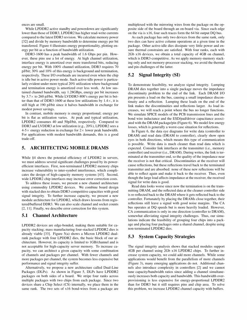
To demonstrate feasibility, we analyze signal integrity. LumpingDRAM dies together into a single package moves the impedancediscontinuity problem to the end of the link. Each DRAM I/Opin presents a load on the bus, causing a small impedance discon-tinuity and a reflection. Lumping these loads on the end of thelink makes the discontinuities and reflections larger. As load in-creases, we will reach a point where the bus no longer functions.We simulate SPICE models of the PCB transmission lines and thebond wire inductance and the ESD/pad/driver capacitance associ-ated with the DRAM package/pin (Figure 6). We model few energylosses, which is generally a worst-case situation for reflections.
In Figure 6, the data eye diagrams for write data (controller toDRAM) and read data (DRAM to controller), clearly show openeyes in both directions, which means this type of communicationis possible. Write data is much cleaner than read data which isexpected. Consider link interfaces at the transmitter (i.e., memorycontroller) and receiver (i.e., DRAM). During writes, the link is ter-minated at the transmitter end, so the quality of the impedance nearthe receiver is not that critical. Discontinuities at the receiver willcause reflections, but these reflections travel back to the terminatedtransmitter and are absorbed: none of these new reflections will beable to reflect again and make it back to the receiver. Thus, eventhough the large load affects impedance at the receiver, the receivedsignal for write data is good.
Read data looks worse since now the termination is on the trans-mitting DRAM, and the reflected data at the cleaner controller sideis re-reflected back to the DRAM where it gets reflected back to thecontroller. Fortunately by placing the DRAMs close together, theirreflections still leave a signal with good noise margins. The CAbus operates at DQ speeds but is more heavily loaded. However,CA communication is only in one direction (controller to DRAM),somewhat alleviating signal integrity challenges. Thus, our simu-lations indicate the feasibility of grouping four chips into a pack-age and placing four packages onto a shared channel, despite usingnon-terminated LPDDR2 dies.
5.3 System Capacity Strategies
The signal integrity analysis shows that stacked modules support4GB per channel using 2Gb x16 LPDDR2 chips. To further in-crease system capacity, we could add more channels. While someapplications would benefit from the parallelism of more channels(Figure 3), many emerging applications do not. Additional chan-nels also introduce complexity in controllers [2] and we cannottune capacity/bandwidth ratios since adding a channel simultane-ously increases both capacity and bandwidth. This bandwidth over-provisioning is less expensive for energy-proportional LPDDR2than for DDR3 but it still requires pins and chip area. To solvethis problem, we increase LPDDR2 channel capacity with buffers.

DDR2 DDR3 LVDDR3 LPDDR LPDDR2Technology Parameter [31] [32, 35] [32, 35] [20, 39] [37, 39]Operating Voltage 1.8V 1.5V 1.35V 1.8V 1.2VOperating Frequency 400MHz 800MHz 400MHz 200MHz 400MHzTypical Device Width (pins) 4 8 8 16 16Peak Channel Bandwidth (sequential) 6.4GBps 12.8GBps 6.4GBps 3.2GBps 6.4GBpsDynamicTiming (CAS, RAS, RC) 12, 40, 55ns 15, 38, 50ns 15, 38, 50ns 12, 40, 54ns 15, 42, 57nsActive Current (read, write) 160, 160mA 180, 185mA 125, 130mA 130, 130mA 210, 175mAEnergy per bit (peak, typical) 111, 266mW/Gbps 70, 160 mW/Gbps 110, 190 mW/Gbps 110, 140 mW/Gbps 40, 50 mW/GbpsStaticIdle current (power-down, standby) 50, 70mA 35, 45mA 22, 32mA 3.6, 20mA 1.6, 23mAMin power-down period 84ns 90ns 90ns 20ns 20nsSlow Powerdown Exit latency 20ns 24ns 24ns 7.5ns 7.5ns
Table 2: Memory technology comparison showing key latency and energy parameters for 2Gb parts.
0
1
0
1
DQ0 DQ11616
CS0CS1
CKE0CKE1
CK
DM
CA10
64 bit D/Q bus
0101
16 16
via
2323
16 16
2323
16 16
via
0101
16 16
via
via
Figure 5: (a) LPDDR2 package with four x16 2Gb devices. (b) Dual Line Package (DLP) architecture with four packages per channel.Each chip select (CS) signal is shared by two devices. Each of the two sets of 16 pins are multiplexed by two devices. Constituentchips of the same rank are indicated by the same rank number (e.g., 0 to 3).
1500
1000
500
0
-500200 400 600 800 1000 1200 1400 1600 1800 2000 2200 24000
Time (ps)
Volta
ge (m
V)
Controller to Device (DQ Write)
1500
1000
500
0
-500200 400 600 800 1000 1200 1400 1600 1800 2000 2200 24000
Time (ps)
Volta
ge (m
V)
Device to Controller (DQ Read)
Figure 6: LPDDR2 signal integrity SPICE simulations with four packages per channel, demonstrating open eyes for controller-memory and memory-controller links. Signal integrity demonstrates feasibility of building the proposed capacity.

6”½”
via
4 2Gb Devicesper Package
Bu�er has 1 C/A bus and 1 D/Q bus from Memory Control-ler. It has 4 C/A busses out to chips on the DIMM, as well as
2 D/Q busses (one for each side of the DIMM.vi
a
via
via
via
via
via
via
via
1 2 3 4
5 6 7 8
C/A to 1,5 C/A to 4,8C/A to 2,6 C/A to 3,7
D/Q to 1,2,5,6D/Q to 3,4,7,8
Figure 7: Channel architecture with load-reduced buffer that allow multiple LPDDR2 packages. Double DQ bus to provide point-point buffer-to-device connections. First line communicates with packages 1, 2, 5, 6. Each via has 16 bits to DQ that are multiplexedby two devices from the same package. Quadruple CA bus, reducing load to two packages per CA line.
Buffers. To hold the number of channels constant and increasechannel capacity, we need to scale either module capacity or thenumber of modules per channel. The former may be difficult dueto packaging constraints. For this reason, we increase the numberof modules per channel. But simply adding modules will overloadthe shared channel and degrade signal integrity.
Following the example of Load-Reduced (LR) DDR3 DIMMs,we propose buffered LPDDR2 DIMMs that buffer and re-time bothDQ and CA buses to ensure signal integrity. The buffer is posi-tioned between the channel and DRAM chips. Chips and bufferscommunicate via point-to-point links to ensure reliable communi-cation even as capacity increases, reducing channel load and per-mitting a larger number of stacked chips. Such buffers can doubleLPDDR2 per channel at modest latency and pin cost.
Figure 7 illustrates our new LPDDR2 module architecture. Thebuffer has 64 DQ and 14 CA pins on the input side. These pinsneed to be duplicated to provide point-point links to the multipleLPDDR2 packages on the board. To double channel capacity from4 to 8GB without compromising signal integrity, the output DQ busneeds to be replicated 2× while the CA bus needs to be replicated4× due to its higher load. We use our new DLPs with packages onboth sides of the board. The capacity can now be scaled by havingmultiple DLPs per channel since the buffer isolates the load on thecontroller and enables multiple buffers per channel. Figure 8 showsthe SI simulations of the proposed 8GB architecture with 8 pack-ages per channel. The signal and timing margins are all sufficientlyhigh for the controller-buffer and buffer-chip lines that allow forreliable communication in the relevant directions.
The proposed load-reduced buffers’ static power overhead issmall since termination is not required for LPDDR2. However,PLLs for clock re-timing incur a small active power cost. Regis-tered DDR3 modules are very common in servers and LRDIMMsare increasingly becoming popular. We envision that our architec-ture for buffered LPDDR2 DLPs will be just as attractive, but withexcellent energy-proportionality.
5.4 Error Correction Strategies
Memory system designers have used Error Correcting Codes(ECC) with Single Error Correction Double Error Detection(SECDED) [48, 52] to detect and correct memory errors. Thesetechniques were originally developed for DRAMs with single bitoutputs, where SECDED would protect from chip failures as well,and used 8 parity bits to protect a 64bit data word. This 72bit in-terface has become a standard, and much work has been done onprotecting wider parts within this form factor. As the width of theDRAM increased, Single Symbol Correct, Double Symbol Detectcodes were used, that could correct a multi-bit symbol, rather thana single bit [5]. Using the B-adjacency algorithm, b bits can be pro-tected through the use of two b-bit wide symbols [18]. While thiscode uses more parity bits, it can be implemented in the same over-head by protecting larger blocks of memory; percentage overheaddecreases as block size increases. These types of algorithms havebeen used to protect DDR3 x4 devices using a block size of 128bits, and have been extended to protect x8 devices.
The wide x16 LPDDR2 interface causes two challenges for ECC.The first is due to quantization: 72 bits is not divisible by 16 and wecannot naturally provide data using the standard memory interface.The second is the larger number of bits needed to protect against aloss of 16 bits. These challenges are similar to those in architecturesthat access fewer chips for energy-proportionality [1, 48, 54], andwe leverage some of their techniques to address these issues.
There are four ways to deal with the quantization issue: makex18 LPDDR2 DRAM, increase the overhead and create an 80/64module, create a 144/128 bit channel, or embed the ECC data intothe memory space. While the first solution seems simple, it wouldgenerate a different DRAM part type, which is expensive. Us-ing x16 parts, we can either use one to protect four or eight otherDRAMs. In the former, we double the parity overhead, which in-creases the cost of the memory by 12.5% but makes protecting fromchip-kill much easier. In the latter, we merge two channels into asingle channel with twice the bandwidth and larger block transfers.
The last option is to maintain a 64 bit interface and embed theECC into the memory space instead of sitting in disparate devices

1000
500
0
-500
-1000
200 400 600 800 1000 1200Time (ps)
Volta
ge (m
V)
Waveform (w/o Xtalk)Fuzzy Band: 54ps, Min Quarter Eye Height: 1211mV, Center Height: 1776mV
-1500
1500
(a) Controller to On-DIMM Buffer
1500
1000
500
0
-500
-1000
-1500200 400 600 800 1000 1200
Time (ps)
Volta
ge (m
V)
Waveform (w/o Xtalk)Fuzzy Band: 15ps, Min Quarter Eye Height: 2022mV, Center Height: 2348mV
(b) Buffer to Controller
1000
500
0
-500
-1000
200 400 600 800 1000 1200Time (ps)
Volta
ge (m
V)
Waveform (w/o Xtalk)Fuzzy Band: 54ps, Min Quarter Eye Height: 1211mV, Center Height: 1776mV
-1500
1500
(c) On-DIMM Buffer to Device DQ
1000500
0-500
-1000
200 400 600 800 1000 1200Time (ps)
Volta
ge (m
V)
Waveform (w/o Xtalk)Fuzzy Band: 454ps, Min Quarter Eye Height: 516mV, Center Height: 1478mV
-1500
150020002500
-2000-2500
(d) Device DQ to On-DIMM Buffer
1000
500
0
-500
-1000
200 400 600 800 1000 1200Time (ps)
Volta
ge (m
V)
Waveform (w/o Xtalk)Fuzzy Band: 400ps, Min Quarter Eye Height: 236mV, Center Height: 800mV
(e) On-DIMM Buffer to Device CA
Figure 8: Signal Integrity analysis for Load-Reduce Buffers to increase channel capacity using LPDDR2 Package Modules. Figure8(a) to Figure 8(e) show open eyes (for reliable communication) using On board buffer.
[54, 52]. The memory controller performs two accesses, one fordata and one for ECC. Embedded ECC does not require dedicatedchips for parity and is energy-efficient. However, memory systemcapacity falls as ECC is embedded in the data space and memorycontroller complexity increases as it must map ECC words. Thisbasic idea is quite flexible, and can support multi-tiered error cor-rection [52], where the OS can determine which pages in memoryonly need error detection (i.e., clean pages) and which need protec-tion and correction. Furthermore, since errors are infrequent, thecorrection data will be accessed infrequently, reducing overheads.This approach is important for modern web applications that maplarge, slowly changing datasets in their memories.
Thus, while LPDDR2 device width causes some challenges forECC, there are many ways these challenges can be addressed. Inour view, it seems likely that some form of multi-tiered error cor-rection will be implemented in these systems, since they are likelyto support chip-kill with modest overhead.
6. EVALUATING EFFICIENCY
LPDDR2 is far more energy-proportional than DDR3 (§4) and thissection shows that LPDDR2 is also far more energy-efficient as itreduces memory power with modest performance penalties.
Power. Using DLPs, we architect a 16GB LPDDR2 systemwith two channels per processor socket. Relative to DDR3 of thesame capacity, LPDDR2 reduces memory system power by 3-5×for our applications (Figure 9(a), Figure 10(a) versus Figure 9(b),Figure 10(b)). Strikingly, LPDDR2 total power is often less thanDDR3 idle power. LPDDR2 also benefits from the fast power-down modes that further reduce background power and that, un-like DDR3, do not require slow DLL re-calibration. In additionto these lower idle overheads, LPDDR2 dynamic power also fallsdue to lower activate current and voltage and fewer chips per ac-cess, which reduce the cost of activates, reads, and writes relative
to DDR3.Datacenter benchmarks, such as websearch and memcached,
show significant power reductions due to their low bandwidth re-quirements. Power falls from approximately 5W to well below 1W,a 5-6× reduction. Other applications, with diverse memory behav-ior, also save memory power. Multiprogrammed benchmarks showa power reduction in the range of 3.3× for 482.sphinx3 to 16.8×for 465.tonto. The savings are proportional to bandwidth, with anaverage power reduction of 4.4× (Figure 2). Significant contrib-utors to this reduction are very low active-idle states and a muchbetter power-down state. Active power is also lower because widerLPDDR2 devices means fewer chips are accessed per cache line.Similarly, multithreaded benchmarks show an average power re-duction of 4.3× in a range of 3.3× for art to 18.8× for ammp.
Performance. Most applications realize significant power sav-ings with modest performance penalties. Figure 10(b), Figure9(b) show application time on an LPDDR2 memory system nor-malized to that on a DDR3 memory system. For instance, theperformance of datacenter workloads like websearch, Memcachedand SPECJbb, SPECpower, and SPECweb is barely affected whenDDR3 is replaced by LPDDR2.
For conventional workloads (SPEC-CPU) multiprogrammedmixes, and PARSEC, SPEC-OMP, the performance impact variesfrom nearly zero for a majority of workloads to a worst case of1.55x. Even when an application is stalled waiting for memory, itmay not have sufficient memory-level parallelism (MLP) to benefitfrom additional sequential memory bandwidth. For example, artis as a memory-bound application with low MLP. However, othermemory-bound workloads (e.g., swim) are impacted by the intro-duction of LPDDR2. Note that any performance penalties arise en-tirely from reduced bandwidth and not latency, which is unchangedwhen adopting LPDDR2 over DDR3. The applications affected bythe lower LPDDR2 bandwidth generally have bursty cache missesthat introduce channel contention.

(a) DDR3-1600 and LVDDR3-800 power, performance. Circlesshow LVDDR-800 performance penalties.
(b) LPDDR2-800 power, performance. See change in y-axis scale.
Figure 9: Datacenter, Multithreaded workloads with 16GB. Idle, termination power are significant in DDR3.
(a) DDR3-1600 and LVDDR3-800 power, performance. (b) LPDDR2-800 power, performance. See change in y-axis scale.
Figure 10: Multiprogrammed workloads with 16GB. x-axis label numbers correspond to Table 1.
Figure 11: DDR3 and LPDDR2 average memory access energy (AMAE) in nJ per memory instruction and average memory accesstime (AMAT) in cycles per memory instruction. Shown for 4, 8, 6, and 32MB L3 cache sizes.

Xeon+DDR3 Atom+DDR3 Xeon+LPDDR2 Atom+LPDDR28-cores 16-cores 8-cores 16-cores
Cost ($) Power (W) Cost ($) Power (W) Cost ($) Power (W) Cost ($) Power (W)Processor (2-socket) 760 125 360 25 760 125 360 25Motherboard 200 30 1340 3 200 30 1340 3Network Interface 0 5 0 5 0 5 0 5Memory (32GB/2-sockets) 600 40 600 40 775 10 775 10Storage (HDD) 100 10 100 10 100 10 100 10Total 1660 210 2400 83 1835 180 2575 53No. Servers (×103, in 15MW) 70 180 83 283TCO ($ per server per month) $86.4 $86.4 $86.4 $86.4Capability 1.0 2.5 1.2 4.0
Table 3: Define TCO-neutral price with Xeon+DDR3 baseline ($86). Atoms use TCO-neutral price for custom board ($1340).Atom+LPDDR2 shows TCO-neutral price for mobile memory ($775 for 32GB). Capability quantifies data center throughput nor-malized against Xeon+DDR3.
Mobile-class LPDDR2-800 performance effects are similar tothose in server-class LVDDR3-800. LVDDR3 lowers the volt-age from 1.5 to 1.35V and also reduces channel frequency. Low-ering the voltage reduces memory core power, but does not ad-dress the inefficiencies of interface circuitry. Lowering the chan-nel frequency also reduces power, but does not address staticpower dissipated by interface circuitry. For the same perfor-mance penalty, (e.g., iso-penalty LVDDR3-800 and LPDDR2-800), LVDDR3 saves much less power. We cannot perform aniso-savings comparison of performance because LVDDR3 cannotmatch LPDDR2’s power savings.
7. PROCESSOR CACHE INTERACTIONS
Memory performance and power efficiency impact processor cachearchitecture. To understand these effects, we introduce AverageMemory Access Energy (AMAE), which is analogous to the conven-tional Average Memory Access Time (AMAT). AMAE provides away to evaluate new memory technologies by combining the effectsof dynamic and static energy in both processor caches and mainmemory. Quantifying the average number of Joules per memory in-struction, AMAEL(i) = EdL(i) + EsL(i) + MRL(i) × AMAEL(i+1).
Dynamic energy for accessing level i in the memory hierarchyis denoted by EdL(i), the miss rate is denoted by MRL(i). EsL(i) isthe total static energy consumed during an application’s executionamortized over the number of memory accesses. CACTI estimatescache energy, DRAMSim estimates activate and read-write energy,and Micron power calculators [32] estimate DQ energy.
In conventional wisdom, the high latency and energy of DRAM,motivates larger processor caches that improve average memory ac-cess time and energy. By reducing memory activity, caches alsoincrease opportunities for DRAM low-power modes while reduc-ing the likelihood of memory contention. However, larger cachesdissipate more static power and are less effective for emerging ap-plications (e.g., web search, memcached). Balancing benefits andcosts requires a holistic view with AMAE.
Figure 11 illustrates AMAE for a variety of L3 cache sizes. Thetrade-offs between dynamic and static energy vary across appli-cations, which are placed along the x-axis in order of decreas-ing memory intensity. Accessing DDR3 is expensive and largercaches mitigate its cost. AMAT falls with cache size, especiallyfor bandwidth-intensive applications. In contrast, the net changein AMAE from larger caches is modest. The increased energy oflarger caches cancels, in large part, reductions in DRAM dynamicenergy (due to fewer accesses) and DRAM static energy (shorterexecution time).
Consuming less energy, LPDDR2 reduces AMAE when com-
pared to DDR3. Lower LPDDR2 energy also magnifies the impactof static energy as L3 cache sizes increase. For many workloads,increasing the cache size leads to flat or increasing AMAE. Al-though larger caches reduce execution time, LPDDR2 is energy-proportional and opportunities to further reduce memory static en-ergy are small. On the other hand, larger caches introduce a newproblem in cache static energy. For AMAE, it is preferable topay the high dynamic energy accessing DRAM rather than ratherthan continuously consume high static energy for a large L3. Mostimportantly, perhaps, we illustrate an analysis framework and anAMAE metric that allows architects to reason about emergingmemory technologies and their interactions with other layers in thecache and memory hierarchy.
8. DATACENTER COST IMPLICATIONS
As servers adopt mobile hardware for efficiency, more of each dol-lar is spent on computing and less is spent on overheads. On theother hand, at least initially, capital costs for mobile hardware maybe higher. Table 3 analyzes these trade-offs, accounting for capi-tal costs in datacenter construction and IT equipment and operatingcosts from power [12, 40]. The model assumes $0.07/kWh, $200Mfacility cost, and a 15MW budget. Facility and IT capital costs areamortized over 15 and 3 years, respectively.
TCO-neutral prices. In the early stages of a new technology(e.g., LPDDR2-based servers) when costs are evolving, end-usersmight more tractably reason about the price they would willinglypay for expected benefits. We define a TCO-neutral price for acomponent as the price that produces a TCO matching some base-line. Our baseline is Xeon+DDR3 (TCO=$86).
Until now, advances in processor efficiency have out-paced thosefor memory. Moreover, simpler OOO cores or in-order cores, suchas mobile Atoms are being considered for servers. Conventionalmotherboards are over-provisioned for such cores motivating sys-tems like the one from SeaMicro, which eliminates 90% of moth-erboard components [30]. By adopting Atoms or other power effi-cient processors, server power falls from 190 to 63W, a 3× reduc-tion. To realize such efficiency, datacenters might willingly pay forcustom boards as long as TCO does not change. Sweeping boardprices, TCO is held to $86 if customization costs less than $1340.
As processor efficiency improves, memory becomes an ef-ficiency bottleneck. DDR3 dissipates 4-5× more power thanLPDDR2 for applications with moderate memory activity, such asweb search. Because mobile memory reduces power costs, dat-acenters might willingly pay a premium for LPDDR2. Sweep-ing LPDDR2 prices, we find Atom+LPDDR2 is justified if mobilememory prices are less than $775 per 32GB, a 30% premium over

Figure 12: Power breakdown across server components.
Figure 13: Total cost of ownership breakdown across servers and infrastructure.
DDR3 prices. This analysis is conservative because it precludesTCO increases, which might be justified by additional datacentercapacity enabled by mobile hardware.
Capacity. Mobile processors and memory shift TCO break-downs (Figure 13). Of each dollar spent, 89% goes to server costsand not infrastructure overheads. In contrast, with Xeon+DDR3servers, only 58% of costs go to servers. Table 3 presents datacentercapacity normalized to Xeon+DDR3 for web search based on pub-lished measurements [40]. Within a 15MW critical load, we candeploy 2.5× more 16-core Atom servers than 8-core Xeon servers,leading to a commensurate capacity increase even when taking intoaccount that an Atom core sustains 0.5× the query throughput ofa Xeon core. Atom+LPDDR2 power is even lower and allows afurther 1.6× increase in the number of servers. Capacity increasesby a cumulative total of 4.0× over Xeon+DDR3.
This analysis assumes no performance penalty from mobilememory. While true for search, which uses less than 10% ofDDR3 peak bandwidth [23], other applications may see perfor-mance penalties that degrade the 1.6× gain from LPDDR2. Forexample, if application performance falls by 20% when using mo-bile memory, the 1.6× increase in servers is offset, in part, by the0.8× impact on per server capacity. Thus, we illustrate a frame-work that allows architects to reason about justifiable prices for thebenefits of emerging technologies.
9. RELATED WORK
To improve the efficiency of server-class memory, Lim et al. com-pare various grades and generations of DDR [26, 27]. These tech-nologies provide modest performance and efficiency trade-offs. Toincrease the dynamic range of these trade-offs, one might reconfig-ure the voltage and frequency of memory systems [6, 8]. Such anapproach allows users to match memory system capabilities to ap-plication demands and increase efficiency. However, voltage scal-ing applies only to the memory core and only in a narrow rangedefined by the device margins. Frequency scaling applies to thememory channel, reducing power, but often increasing the energyper bit because of the static power component.
A large body of work manages data placement [10, 24, 47, 9,38, 16] and batches memory requests [7, 17] to increase the lengthof idle periods, which are necessary to exploit power modes that
have long exit latencies. Despite these techniques, DDR powermodes often incur performance penalties due to batching and thelatency of the critical word is always affected. Although many ofthese techniques could be applied to LPDDR2, mobile-class powermodes have much shorter exit latencies, effectively eliminating theproblem these techniques try to solve. With faster transitions be-tween power modes, LPDDR2 provides more opportunities to ex-ploit them or simpler control heuristics to manage them.
Seeking to improve energy proportionality, other researcherswork to narrow the access width of a memory operation. Insteadof accessing a wide row that spans multiple KB, they access asmaller subset [1, 48, 51, 54]. However, rank subsetting signifi-cantly increases the amount of peripheral circuitry in a chip, de-grading density [49]. In contrast, LPDDR technologies use thesame DDR memory core, achieving comparable densities. LPDDRonly changes the interface circuitry, addressing the power over-heads in chip I/O, the largest efficiency bottleneck in DRAMs [49].
10. CONCLUSION
Many data center applications under-utilize the memory bandwidthavailable in modern servers. We presented an alternative design forserver memory systems that uses commodity DRAM chips for mo-bile applications. These memory systems tradeoff peak bandwidthfor significant gains in energy efficiency and proportionality. Wehave shown that LPDDR2 based servers provide high capacity andsmall performance impact for data center workloads.
11. ACKNOWLEDGMENTS
We sincerely thank David Lo, Jacob Leverich, Daniel Sanchez,Scott Best and Wayne Richardson for their useful feedback anddiscussion. Krishna Malladi is supported by Benchmark-CapitalStanford Graduate Fellowship. This work is supported in part byNSF grant CCF-1149252.
12. REFERENCES[1] J. Ahn et al. Future scaling of processor-memory interfaces.
In SC, 2009.[2] M. Awasthi et al. Handling the problems and opportunities
by multiple on-chip memory controllers. In PACT, 2011.

[3] L. Barroso et al. The case for energy proportional computing.IEEE Computer, 2007.
[4] A. Bosque et al. Characterization of Apache web server withSpecweb2005. In MEDEA, 2007.
[5] Bossen et al. b-adjacent error correction. IBM Journal ofResearch and Development, 1970.
[6] H. David, O. Mutlu, et al. Memory power management viadynamic voltage/frequency scaling. In ICAC, 2011.
[7] V. Delaluz et al. DRAM energy management using software& hardware directed power mode control. In HPCA, 2001.
[8] Q. Deng et al. Memscale: Active low-power modes for mainmemory. In ASPLOS, 2011.
[9] B. Diniz, D. Guedes, and R. Bianchini. Limiting the powerconsumption of main memory. In ISCA, 2007.
[10] X. Fan, C. Ellis, and A. Lebeck. Memory controller policiesfor DRAM power management. In ISLPED, 2001.
[11] B. Ganesh et al. FB DIMM memory architectures:Understanding mechanisms, overheads, & scaling. In HPCA,2007.
[12] J. Hamilton. Cost of power in large-scale data centers.http://perspectives.mvdirona.com.
[13] H. Hanson et al. What computer architects need to knowabout memory throttling. In WEED, 2010.
[14] Hewlett-Packard. DDR3 memory technology. Technologybrief TC100202TB, Hewlett-Packard, 2010.
[15] U. Hoelzle and L. Barroso. The Datacenter as a Computer.Morgan and Claypool, 2009.
[16] H. Huang et al. Improving energy efficiency by makingDRAM less randomly accessed. In ISLPED, 2005.
[17] I. Hur and C. Lin. A comprehensive approach to DRAMpower management. In HPCA, 2008.
[18] B. Jacob et al. Memory Systems: Cache, DRAM, Disk.Morgan Kaufmann, 2007.
[19] A. Jaleel et al. High performance cache replacement usingre-reference interval prediction (RRRIP). In ISCA, 2010.
[20] JEDEC. JEDEC standard for LP-DDR2. StandardJESD209-2B, JEDEC, 2010.
[21] B.-H. Jeong et al. A 1.35V 4.3GB/s 1Gb LPDDR2 DRAMwith controllable repeater and on-the-fly power-cut schemefor low-power and high-speed mobile application. In ISSCC,February 2009.
[22] Kim et al. Thread cluster memory scheduling: Exploitingdifferences in memory access behavior. In MICRO, 2010.
[23] C. Kozyrakis, S. Sankar, et al. Server Engineering Insightsfor Large-Scale Online Services. IEEE Micro, 2010.
[24] A. Lebeck, X. Fan, H. Zeng, , and C. Ellis. Power awarepage allocation. In ASPLOS, 2000.
[25] S. Li et al. McPaT: An integrated power, area, and timingmodeling framework for multicore and manycorearchitectures. In MICRO, 2009.
[26] K. Lim et al. Understanding and designing new serverarchitectures for emerging warehouse-computingenvironments. In ISCA, 2008.
[27] K. Lim et al. Disaggregated memory for expansion andsharing in blade servers. In ISCA, 2009.
[28] C. Luk et al. Pin: Building customized program analysistools with dynamic instrumentation. In PLDI, 2005.
[29] D. Meisner, B. Gold, and T. Wensich. PowerNap:Eliminating server idle power. In ISCA, 2009.
[30] R. Merritt. Startup SeaMicro packs 512 Intel Atoms in
server. EE Times, 2010.[31] Micron. Calculating memory system power for DDR2.
Technical Note tn4704, Micron, 2005.[32] Micron. Calculating memory system power for DDR3.
Technical Note TN-41-01, Micron, 2007.[33] Micron. 152-ball x32 mobile lpddr pop (ti-omap). Data Sheet
MT46HxxxMxxLxCG, Micron, 2008.[34] Micron. Micron 1Gb: x16, x32 Mobile LPDDR SDRAM.
Data Sheet MT46H32M32LF-5, Micron, 2010.[35] Micron. Micron 2Gb: x4, x8, x16 DDR3 SDRAM. Data
Sheet MT41J128M16HA-125, Micron, 2010.[36] J. Ousterhout et al. The case for RAMClouds:scalable
high-performance storage entirely in DRAM. SIGOPS, 2010.[37] R. Palmer et al. A 4.3GB/s mobile memory interface with
power-efficient bandwidth scaling. In VLSI, 2009.[38] V. Pandey, W. Jiang, Y. Zhou, and R. Bianchini. DMA-aware
memory energy management. In HPCA, 2006.[39] Rambus. Mobile XDR memory versus LPDDR2.
http://www.rambus.com/us/technology/solutions/mobile_xdr/mxdr_vs_lpddr2.html.
[40] V. Reddi et al. Web search using mobile cores: Quantifyingand mitigating the price of efficiency. In ISCA, 2010.
[41] B. Rogers, A. Krishna, G. Bell, K. Vu, X. Jiang, andY. Solihin. Scaling the bandwidth wall: Challenges in andavenues for CMP scaling. In ISCA, 2009.
[42] P. Saab. Scaling memcached at Facebook. FacebookEngineering Note, 2008.
[43] R. Schmitt et al. Signal and power integrity limitations formobile memory in 3D packaging. EE Times, 2010.
[44] N. Sharma, S. Barker, D. Irwin, and P. Shenoy. Blink:Managing server clusters on intermittent power. In ASPLOS,2011.
[45] K. Shiv et al. SPECjvm2008 performance characterization.In SPEC Benchmark Workshop on Computer PerformanceEvaluation and Benchmarking, 2009.
[46] L. Tang et al. The impact of memory subsystem resourcesharing on datacenter applications. In ISCA, 2011.
[47] M. Tolentino et al. Memory MISER: Improving mainmemory energy efficiency in servers. IEEE Trans, 2009.
[48] A. Udipi et al. Rethinking DRAM design and organizationfor energy-constrained multi-cores. In ISCA, 2010.
[49] T. Vogelsang. Understanding the energy consumption ofdynamic random access memories. In MICRO, 2010.
[50] D. Wang et al. DRAMSim2: A cycle accurate memorysystem simulator. IEEE Comput. Archit. Letters, 2011.
[51] F. Ware and C. Hampel. Improving power and data efficiencywith threaded memory modules. In ICCD, 2006.
[52] D. H. Yoon and M. Erez. Virtualized and flexible ecc formain memory. In ASPLOS, 2010.
[53] L. Zhao et al. Exploring Large-Scale CMP Architcturesusing Manysim. IEEE Micro, 2007.
[54] H. Zheng et al. Mini-rank: Adaptive DRAM architecture forimproving memory power efficiency. In MICRO, 2008.