Embed Size (px)
Citation preview
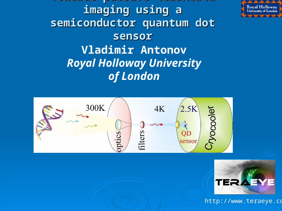
Towards passive terahertz Towards passive terahertz imaging using a imaging using a
semiconductor quantum dot semiconductor quantum dot sensorsensor
Vladimir AntonovRoyal Holloway
University of London
http://www.teraeye.com
AcknowledgmentsAcknowledgments
Royal Holloway, UK : H Hashiba
Tokyo University&JST, Japan: Prof. S Komiyama, Drs. J Chen, O Astafiev (NEC)
ISSP RAN, Russia: Dr. L Kulik
NPL, UK: Dr A Tzalenchuk, Dr S Gibling and P Kleinschmidt
Chalmers University, Sweden: Prof. P Delsing, Dr S Kubatkin
Optisense LTD: M Andreo
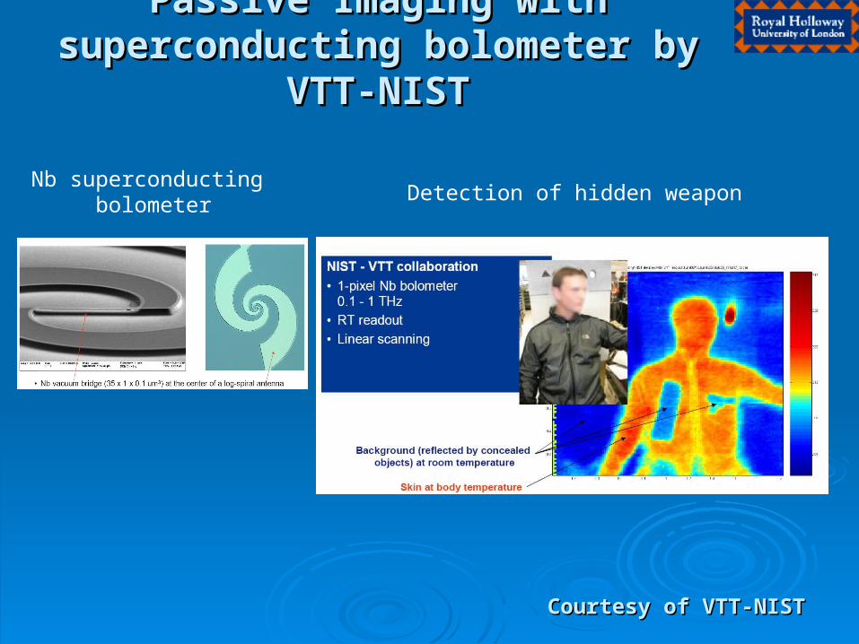
Passive Imaging with Passive Imaging with superconducting bolometer by superconducting bolometer by
VTT-NISTVTT-NIST
Nb superconducting bolometer Detection of hidden weapon
Courtesy of VTT-NISTCourtesy of VTT-NIST
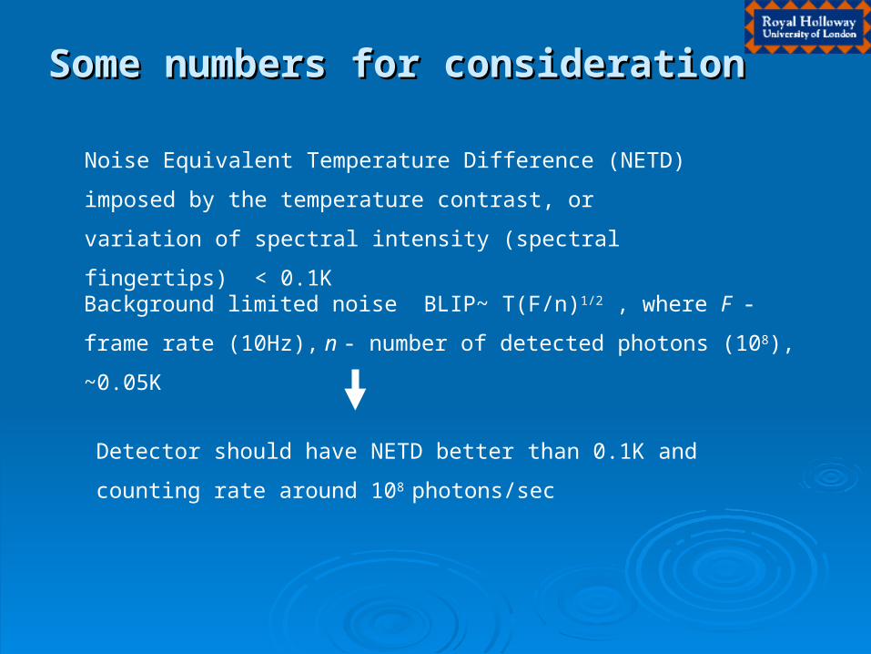
Some numbers for considerationSome numbers for consideration
Background limited noise BLIP~ T(F/n)1/2 , where F - frame rate
(10Hz), n - number of detected photons (108), ~0.05K
Noise Equivalent Temperature Difference (NETD)
imposed by the temperature contrast, or variation of
spectral intensity (spectral fingertips) < 0.1K
Detector should have NETD better than 0.1K and
counting rate around 108 photons/sec
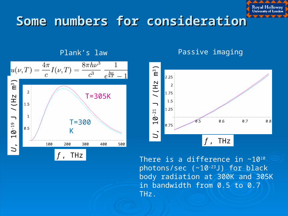
Some numbers for considerationSome numbers for consideration
Plank’s law
100 200 300 400 500
0.5
1
1.5
2T=305K
T=300K
f , THz
U,
10-1
9 J
/(H
z m
3 )
There is a difference in ~1010 photons/sec (~10-23J) for black body radiation at 300K and 305K in bandwidth from 0.5 to 0.7 THz.
Passive imaging
0.5 0.6 0.7 0.80.75
1.25
1.5
1.75
2
2.25
U,
10-2
1 J
/(H
z m
3 )
f , THz
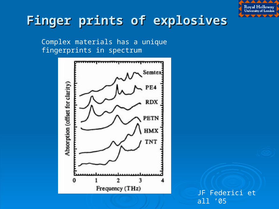
Finger prints of explosivesFinger prints of explosives
Complex materials has a unique fingerprints in spectrum
T=300K
JF Federici et all ’05
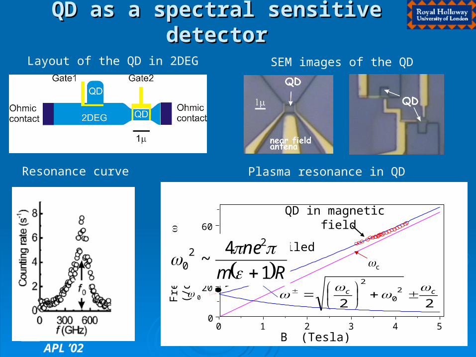
QD as a spectral sensitive QD as a spectral sensitive detectordetector
Layout of the QD in 2DEG SEM images of the QD
222
0
2
cc
B (Tesla)0 1 2 3 4 5
0
20
40
60
Fre
quen
cy
(/c
m)
c
0
QD in magnetic field
Zero filed
Plasma resonance in QD
Rm
ne
1
4~
22
0
Resonance curve
APL ’02
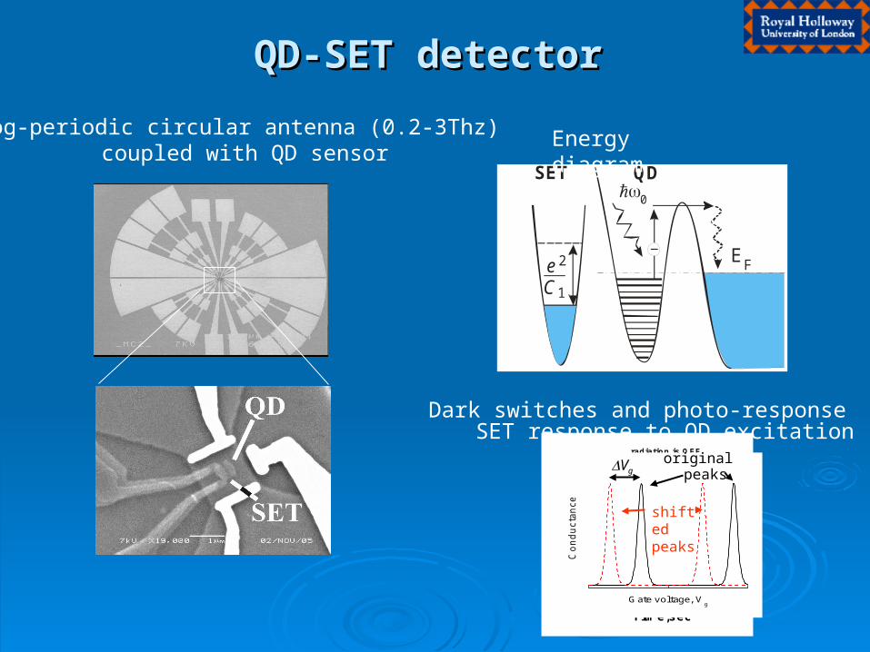
QD-SET detectorQD-SET detector
eC1
2
0
EF
QDSET
Energy diagram
Dark switches and photo-response
radiation is ON
radiation is OFF
SE
T c
urr
ent,
arb
7525
Time,sec
Log-periodic circular antenna (0.2-3Thz) coupled with QD sensor
Conduct
ance
Gate voltage, Vg
original peaks
shifted peaks
Vg
SET response to QD excitation
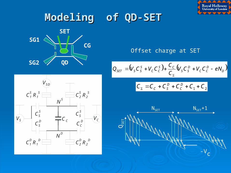
Modeling of QD-SETModeling of QD-SET
CSD
CCD
CSS
CSS
C1S
R1S
C2S
R2S
C1D
R1D
C2D
R2D
ND
NS
VS VC
VSD
CC
CGSG1
SG2
SET
QD D
DCC
DSS
CSCC
SSSSET eNCVCV
C
CCVCVQ
Offset charge at SET
21 CCCCCC DC
DSC
QSE
T
NSET NSET+1
-Vc
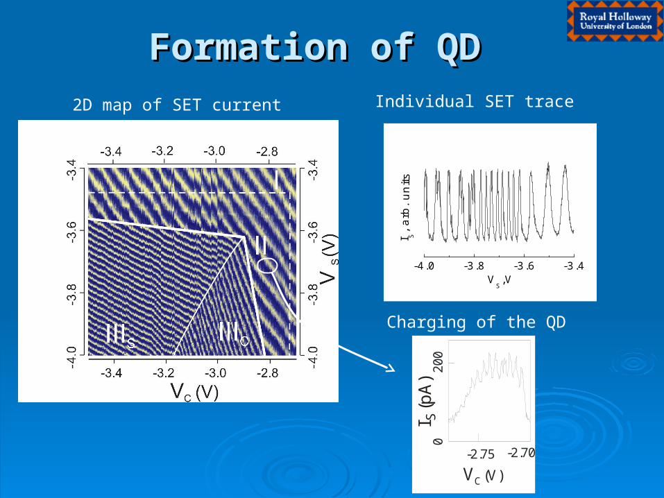
Formation of QDFormation of QD
020
0-2.75 -2.70
VC (V)
I (p
A)
S
ICharging of the QD
-4.0 -3.8 -3.6 -3.4V
S,V
I S, a
rb. u
nits
2D map of SET current Individual SET trace
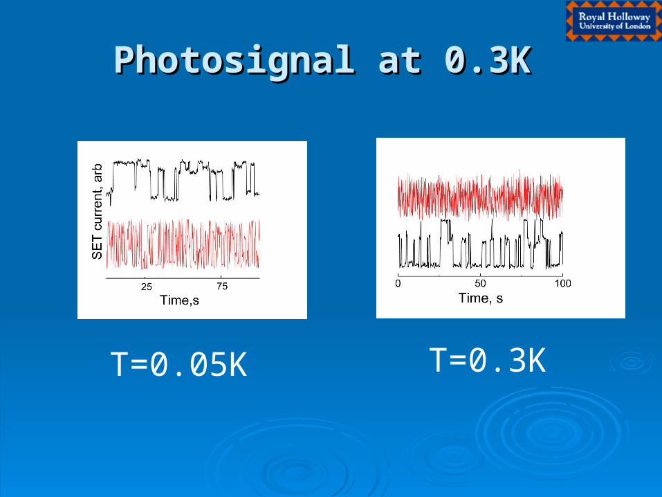
Photosignal at 0.3KPhotosignal at 0.3K
T=0.05K T=0.3K
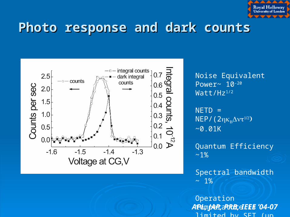
Photo response and dark counts Photo response and dark counts
APL, JAP, PRB, IEEE ’04-07
Noise Equivalent Power~ 10-20 Watt/Hz1/2
NETD = NEP/(2~0.01K
Quantum Efficiency ~1%
Spectral bandwidth ~ 1%
Operation temperature is limited by SET (up to 4K)
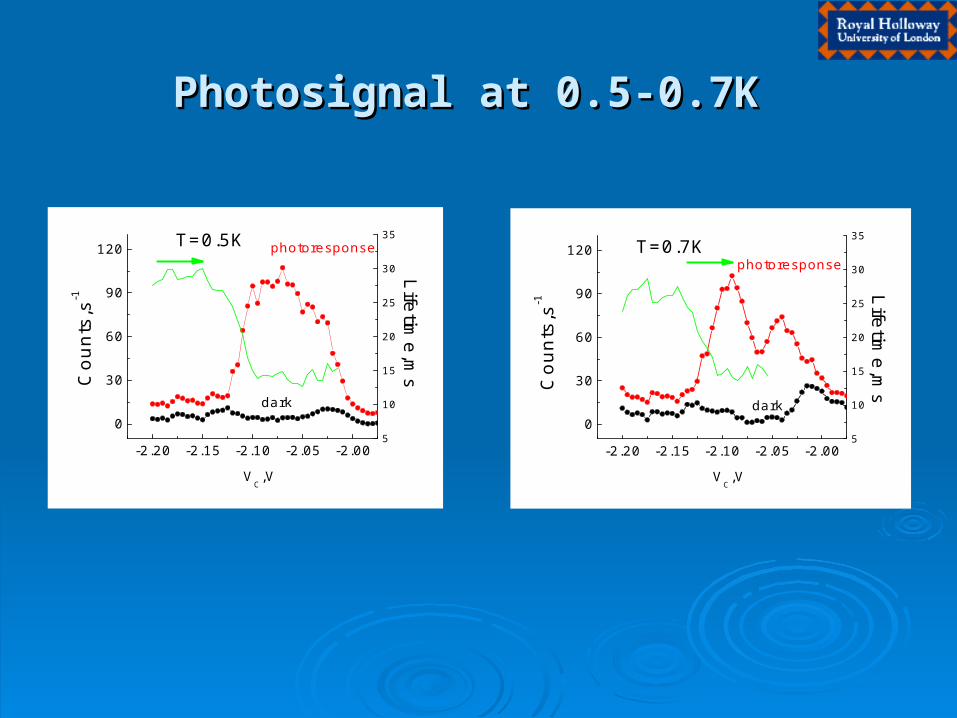
Photosignal at 0.5-0.7KPhotosignal at 0.5-0.7K
5
10
15
20
25
30
35
-2.20 -2.15 -2.10 -2.05 -2.00
0
30
60
90
120
Co
un
ts,s
-1
VC,V
Life
time
,ms
T=0.7Kphotoresponse
dark
5
10
15
20
25
30
35
-2.20 -2.15 -2.10 -2.05 -2.00
0
30
60
90
120
Cou
nts,
s-1
VC,V
Lifetime,m
s
T=0.5K photoresponse
dark
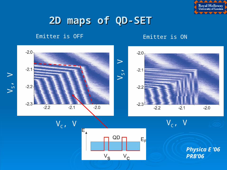
2D maps of QD-SET 2D maps of QD-SET
Emitter is ON
VC, VV
S,
V
Physica E ’06PRB’06
Emitter is OFF
VC, V
VS,
V
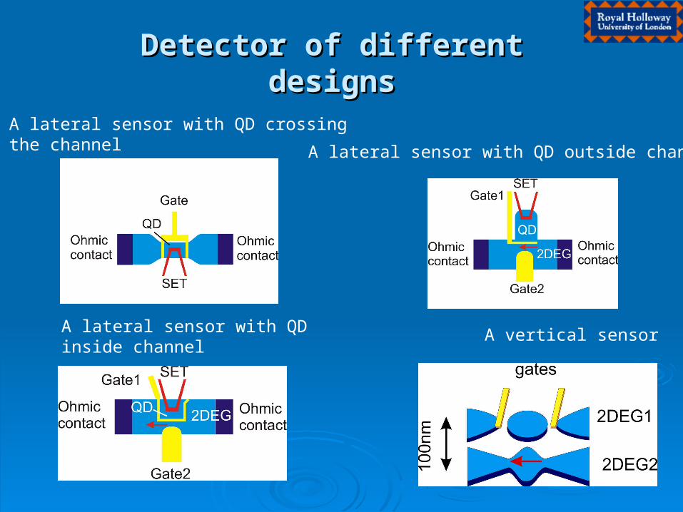
Detector of different Detector of different designsdesigns
A vertical sensor
A lateral sensor with QD crossing the channel
A lateral sensor with QD inside channel
A lateral sensor with QD outside channel
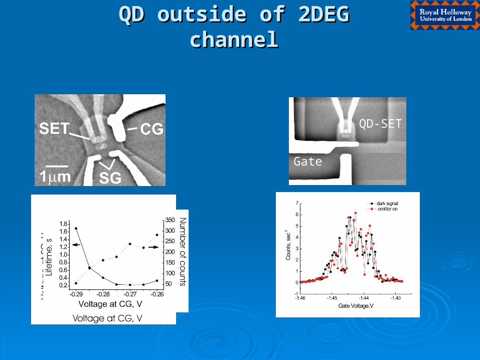
QD outside of 2DEG QD outside of 2DEG channelchannel
Gate
QD-SET
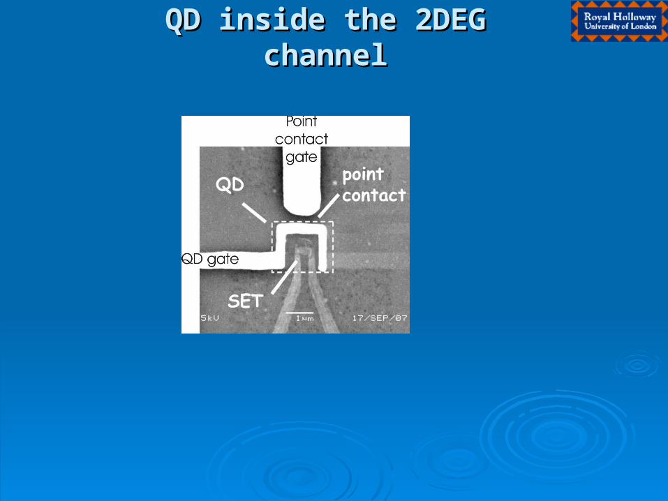
QD inside the 2DEG QD inside the 2DEG channelchannel
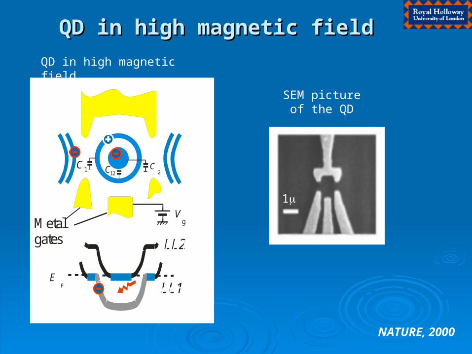
QD in high magnetic fieldQD in high magnetic field
CC 112
C2
Metal gates
Vg
EF LL1
LL2
LL0
LL1
NATURE, 2000
QD in high magnetic field
1
SEM picture of the QD
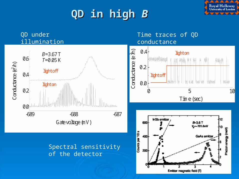
QD in high QD in high BB
light off
light on
-689 -688 -6870.0
0.2
0.4
0.6
Con
duct
ance
(e2 /h
)
Gate voltage (mV)
B=3.67 TT=0.05 K
0 5 10Time (sec)
light off
light on
Con
duct
ance
(e /h
)2
0.0
0.2
0.4
QD under illumination Time traces of QD conductance
Spectral sensitivity of the detector
QD in high QD in high BB
B(Tesla)
3.5
II II II II II II II II II II II
I I I I I I I II
3.73.6
-660
-665
-670
Con
trol
gat
e vo
ltage
(m
Vol
t)
Con
dact
ance
(arb
.uni
ts)
0
1
QD has three levels: LL0LL0LL1
I IILifetime of excitations
3.4 3.6 3.8 4.0 4.210
-3
10-2
10-1
1
101
102
103
104
6
98
7 5
43
2 1
Life
time
(s)
B (T)
PRB, 2002
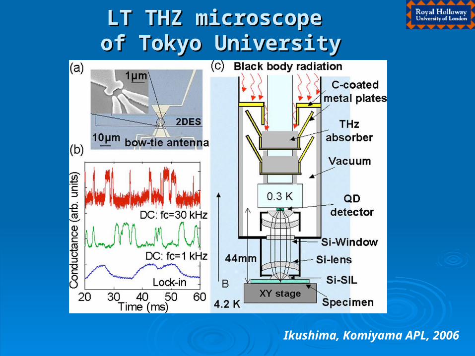
LT THZ microscope LT THZ microscope of Tokyo Universityof Tokyo University
Ikushima, Komiyama APL, 2006
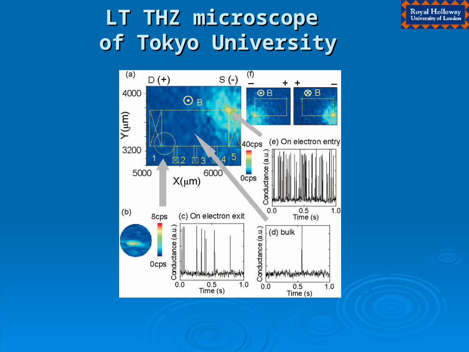
LT THZ microscope LT THZ microscope of Tokyo Universityof Tokyo University
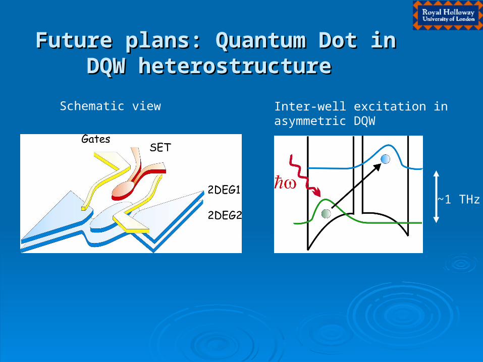
Future plans: Quantum Dot in Future plans: Quantum Dot in DQW heterostructure DQW heterostructure
~1 THz
Schematic view Inter-well excitation in asymmetric DQW
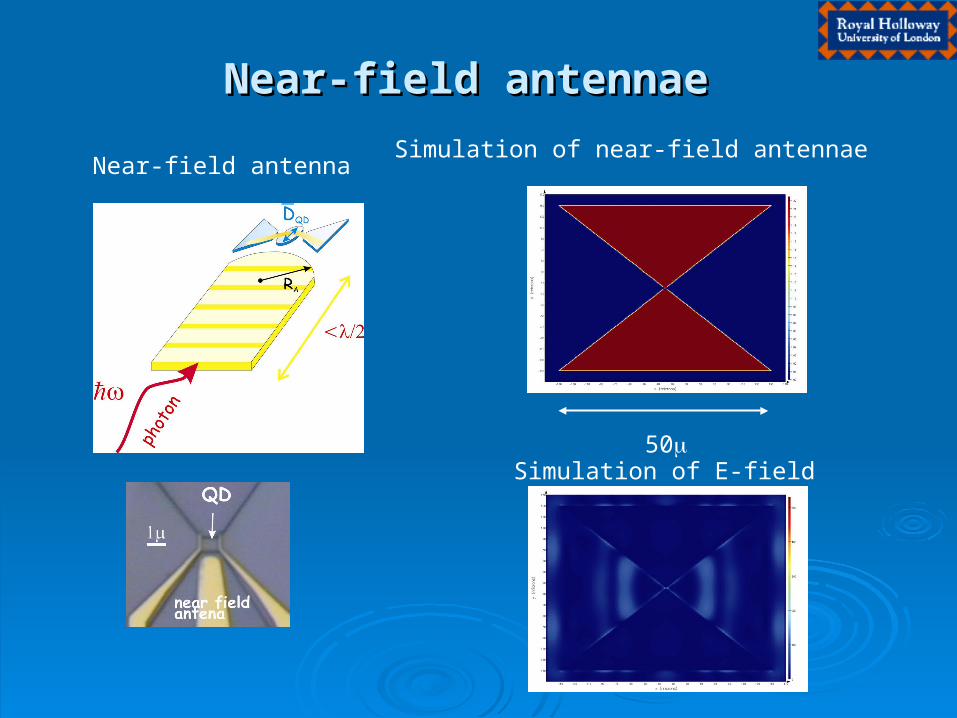
Near-field antennaeNear-field antennae
50
Simulation of near-field antennae
Simulation of E-field
Near-field antenna
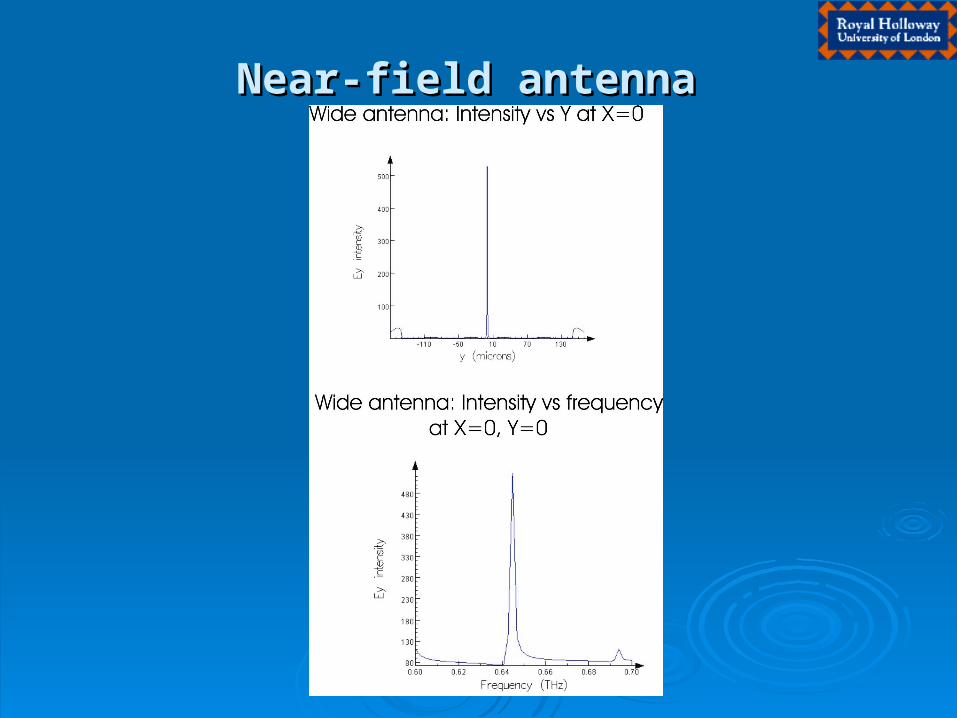
Near-field antennaNear-field antenna
Challenges Challenges
QD detector: which type?
Room Temperature Imaging
Source of THz radiation for in-situ calibration
• Physics of isolated QD in DW heterostructures
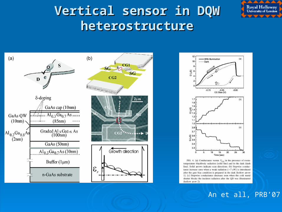
Vertical sensor in DQWVertical sensor in DQWheterostructureheterostructure
An et all, PRB’07