Embed Size (px)
Citation preview
Towards a Monolithic, Substrate-Reusable and an All-Epitaxial Design for III-V-on-Si Solar Cells
Nikhil Jain, Michael Clavel, Patrick Goley, and Mantu Hudait
Virginia Tech, Blacksburg, VA 24060
Abstract - Integration of III-V multijunction solar cells on
Si substrate can address the future levelized cost of energy by
unifying the high-efficiency merits of III-V materials with the
low-cost and abundance of Si. A Si-compatible monolithically
integrated 3J InGaP/GaAs/Ge-Si cell design with a hybrid
Ge-Si bottom cell is investigated. Utilizing a combination of
comprehensive modeling and experimental material
characterization techniques, we present our results for ultra
thin epitaxial Ge directly grown on Si substrate using
molecular beam epitaxy. Virtual "Ge-on-Si" substrates could
provide a large-area, low-cost alternative to expensive GaAs
wafers, a promising step towards realizing monolithic, high
efficiency and low-cost III-V-on-Si photovoltaics.
Index Terms - III-V-on-Si, Ge-on-Si, heteroepitaxy,
photovoltaic cells, solar cell design.
I. INTRODUCTION
While the efficiency of mainstream Si based solar cells has almost saturated at �25%, III-V multijunction solar cells have steadily shown performance improvement, reaching a recent record efficiency of 46%. Integration of such III-V multijunction cells with Si can address the future levelized cost of energy by unifying the high-efficiency merits of III-V materials with low-cost and abundance of Si. To date, efficiency of 3J III-V/Si tandem solar cells have merely exceeded 25% [1] even after employing non-monolithic techniques such as wafer-bonding [2] and areal currentmatching [3]. Challenges associated with material growth, reliability and reproducibility have limited the success of IIIV-on-Si technology. Thus, novel approaches are sought for realizing the potential of III-V-on-Si multijunction solar cells.
A very promising path for monolithic integration of III-V solar cells on Si would be to utilize a thin intermediate Ge buffer layer. Successful demonstration of virtual "Ge-on-Si" template could significantly reduce the cost per watt attributed to the large area and low cost of Si substrate. Interestingly, utilizing Ge intermediate layer de-couples two critical challenges for GaAs-on-Si growth: (i) polar on non-polar epitaxy and (ii) lattice-mismatch growth. Owing to a small band gap, the Ge layer absorbs a wide spectrum of the incident sunlight beyond the GaAs absorption edge, and therefore the hybrid Ge-Si subcell does not limit the current in 3J InGaP/GaAs/Ge-Si solar cells. The Ge intermediate layer approach for III-V-on-Si integration could be utilized (i) to create virtual "Ge-on-Si" template for subsequent GaAs growth (could potentially involve active Ge subcells), (ii)
978-1-4799-7944-8/15/$31.00 ©2015 IEEE
solely as a buffer layer for connecting III-V cells to an active Si bottom subcell, and (iii) as the emitter layer for bottom Si base, forming a hybrid Ge-Si subcell.
Utilizing a Si homojunction cell beneath the Ge buffer layer would likely require a diffusion process and a thicker Si substrate for current-matching in comparison to the hybrid GeSi approach. Furthermore, to allow sufficient light penetration to active Si subcell, extremely thin Ge buffer would be essential, rendering the subsequent GaAs growth very challenging. Prior reports on Ge integration on Si substrate for photovoltaics typically employed graded SixGel-x buffers, which were several microns thick [4-6], elevating the thermal mismatch and cost issues. While other approaches utilized a patterned selective area epitaxy [7, 8], typically involving an additional patterning and/or chemical polishing step. Here, we focus on developing a non-selective area Ge-on-Si epitaxial process with a key goal of realizing thin epitaxial Ge layers allowing light penetration to the bottom Si substrate cell.
Thus, in this work we focus on the design, modeling and epitaxial growth for hybrid Ge-Si bottom subcell, wherein the epitaxial Ge layer serves as a uniformly doped emitter for bottom Si subcell, thus forming a hybrid Ge-Si subcell. This approach precludes the need for diffused Si junction, allowing an in-situ and an all-epitaxial process for subsequent III-V growth requiring very thin Si « 60Ilm). Such 3J cells with very thin Si would also be very promising for CPV applications and could further benefit from additional cost
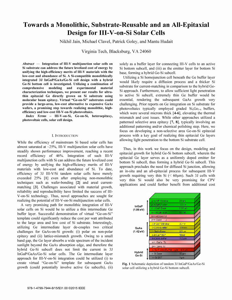
InGaP I (1.86eV)
Hybrid I Ge-Si •••• Fig. 1 Schematic depiction of tandem 3J InGaP/GaAs/Ge-Si
solar cell utilizing a hybrid Ge-Si bottom subcell.
savings by leveraging substrate re-use schemes utilizing amorphous Si (a-Si) as a release layer and additionally as a seed layer for subsequent Si epitaxy [9].
II. SIMULA nON AND EXPERIMENTAL METHODS
The numerical simulations of the proposed 31 InGaP/GaAs/Ge-Si solar cell structure and the band-alignment simulations were performed using APSYS software and schematic of the proposed 31 solar cell structure which utilizes a hybrid Ge-Si bottom subcell is shown in Fig. 1. An ideal anti-reflection coating was assumed for modeling the solar cell. Although, finite element analysis based solar cell modeling has been performed for III-V-on-Si solar cells [10,
11], we report the first study on III-V-on-Si multijunction solar cell modeling using an intermediate Ge layer.
The Ge layers were grown directly on (100) Si substrate with 6° offcut towards the <110> direction in a dual-chamber molecular beam epitaxy (MBE) cluster tool. One of the chambers is solely dedicated for Ge epitaxy and is connected to a separate MBE chamber for III-V epitaxy via an in-situ
ultra-high vacuum transfer chamber. This unique growth capability enables superior Ge epilayer quality with precise thickness control and minimal cross-contamination. The Si substrates were immediately loaded into the load lock of MBE chamber after RCA cleaning. Silicon oxide desorption was performed in the absence of arsenic over pressure at a substrate thermocouple temperature of �950°C in III-V growth chamber. The substrate was cooled to 150°C and then transferred via an ultra-high vacuum transfer chamber to the Ge MBE chamber for subsequent Ge epitaxy. Three epitaxial Ge structures were directly grown on (lOO)Si substrates: (1) 1-step low-temperature (LT) 250°C epitaxial Ge (Sample A), (ii) I-step high-temperature (HT) 400°C epitaxial Ge (Sample B), and (iii) two-step LT/HT epitaxial Ge � 135 nm thick (Sample C). A growth rate of �0.025I1m per hour was utilized for Ge epitaxy and following the Ge growth, the sample was slowly cooled down to prevent any thermal cracking prior to unloading for material characterization.
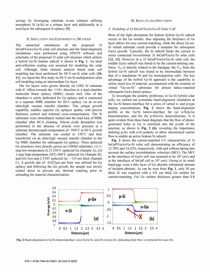
0.8
0.6 0.4
> 0.2 Qj --0 &0 -0.2 ...
Qj c -0.4
w -0.6
-0.8 -1
p-Ge I- ..-
n-Si
.J (a) o 0.5 1 1.5 2 2.5 3 3.5 4
Dista nce h1m)
III. RESULTS AND DISCUSSION
A. Modeling of 3J InGaPIGaAsIGe-Si Solar Cell
Most of the light absorption for bottom hybrid Ge-Si subcell occurs in the Ge emitter, thus adjusting the thickness of Ge layer allows for easy current-matching, while the direct Ge-onSi virtual substrate could provide a template for subsequent GaAs growth. Typically, the Si subcell limits the current in series connected two-terminal 31 InGaP/GaAsllSi solar cells [12, 13]. However in a 31 InGaP/GaAs/Ge-Si so�ar
. �ell, the
middle GaAs subcell was found to be the current-hmltmg one. Since, Voc is directly related to the bandgap, the V oc from the hybrid Ge-Si subcell was found to be intermediate between that of a standalone Si and Ge homojunction cells. The key advantage of the hybrid Ge-Si approach is the capability to utilize much less Si material, accompanied with the creation of virtual "Ge-on-Si" substrates for almost lattice-matched subsequent GaAs based epitaxy.
To investigate the polarity preference in Ge-Si hybrid solar cells, we carried out systematic band-alignment simulation at the Ge-Si hetero-interface for a series of varied n- and p-type doping concentrations. Fig. 2 shows the band-alig�ent profile at the Ge/Si hetero-interface for (a) n-Sl/p-�e heterostructure, and for (b) p-Si/n-Ge heterostructure. It IS quite evident from these band diagrams that the flow of photogenerated holes in Ge is restricted into the p-side of the j unction, as shown in Fig. 2 (b), revealing the
. importa�ce
utilizing p-Ge with n-Si polarity to allow unrestrIcted carner flow to enable an active bottom Si subcell.
Fig. 3 shows the current-matched I-V characteristic of 31 InGaP/GaAs/Ge-Si solar cell demonstrating an efficiency of 32.70% and 34.42%, respectively, with and without taking into account the surface recombination velocities (SRV). The SRV at the interfaces of GaAs cell was assumed to be 106 cm/s and at the interfaces of InGaP cell as 104 cm/s. Owing to its small band-gap, even a thin layer of Ge absorbs substantial amount of incident photons. As can be seen from Fig. 1, only 50 11m thick Si was required with a 0.8 11m thick Ge emitter for current-matching. For Ge emitter thickness greater than 0.8
1
0.5 p-Si 0
-0.5 n-Ge
-1 X (b) -1 .5
0 0.5 1 1.5 2 2.5 3 3.5 4 Distance h1m)
Fig. 2 Band-alignment at Ge/Si heterointerface: (a) p-Ge/n-Si, and (b) n-Ge/p-Si, indicating hole flow is restricted for case (b).
978-1-4799-7944-8/15/$31.00 ©2015 IEEE
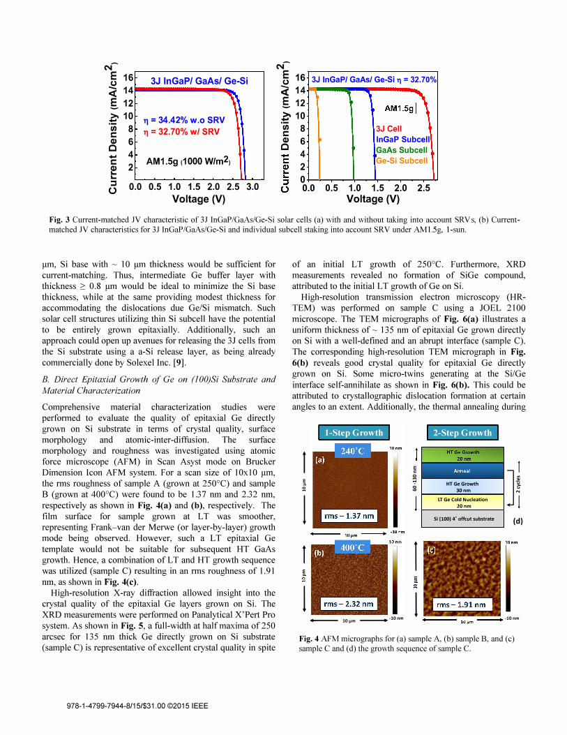
N�
E 16 (.) - 14 « §. 12 � 10 en 8 c: Q) C
6 - 4 c: � 2 ...
3J InGaP! GaAs! Ge-Si
" Tt = 34.42% w.o SRV Tt = 32.70% wI SRV
I AM1.5g (1000 W/m2) I
::::J (J 0.0 0.5 1.0 1.5 2.0 2.5 3.0
Voltage (V)
N�
E 16 (.) 3J InGaPI GaAsl Ge-Si TJ = 32.70%
« 14 §. 12 � 10 en 8 c: Q) 6 C 4
2 o 0.0
-, 1 I AM1.591;
3J Cell InGaP Subcell GaAs Subcell Ge-Si Subcell
0.5 1.0 1.5 2.0 Voltage (V)
2.5
Fig. 3 Current-matched JV characteristic of 3J InGaP/GaAs/Ge-Si solar cells (a) with and without taking into account SRVs, (b) Current
matched JV characteristics for 3J InGaP/GaAs/Ge-Si and individual subcell staking into account SRV under AMI.Sg, I-sun.
J.tm, Si base with � 10 J.tm thickness would be sufficient for current-matching. Thus, intermediate Ge buffer layer with thickness 2: 0.8 J.tm would be ideal to minimize the Si base thickness, while at the same providing modest thickness for accommodating the dislocations due Ge/Si mismatch. Such solar cell structures utilizing thin Si subcell have the potential to be entirely grown epitaxially. Additionally, such an approach could open up avenues for releasing the 3J cells from the Si substrate using a a-Si release layer, as being already commercially done by Solexel Inc. [9].
B. Direct Epitaxial Growth of Ge on (100)Si Substrate and
Material Characterization
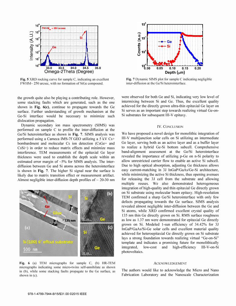
Comprehensive material characterization studies were performed to evaluate the quality of epitaxial Ge directly grown on Si substrate in terms of crystal quality, surface morphology and atomic-inter-diffusion. The surface morphology and roughness was investigated using atomic force microscope (AFM) in Scan Asyst mode on Brucker Dimension Icon AFM system. For a scan size of lOxl0 J.tm, the rms roughness of sample A (grown at 250°C) and sample B (grown at 400°C) were found to be l.37 nm and 2.32 nm,
respectively as shown in Fig. 4(a) and (b), respectively. The film surface for sample grown at L T was smoother, representing Frank-van der Merwe (or layer-by-layer) growth mode being observed. However, such a L T epitaxial Ge template would not be suitable for subsequent HT GaAs growth. Hence, a combination of L T and HT growth sequence was utilized (sample C) resulting in an rms roughness of l.91 nm, as shown in Fig. 4(c).
High-resolution X-ray diffraction allowed insight into the crystal quality of the epitaxial Ge layers grown on Si. The XRD measurements were performed on Panalytical X'Pert Pro system. As shown in Fig. 5, a full-width at half maxima of 250 arcsec for 135 nm thick Ge directly grown on Si substrate (sample C) is representative of excellent crystal quality in spite
978-1-4799-7944-8/15/$31.00 ©2015 IEEE
of an initial L T growth of 250°C. Furthermore, XRD measurements revealed no formation of SiGe compound, attributed to the initial LT growth of Ge on Si.
High-resolution transmission electron microscopy (HRTEM) was performed on sample C using a JOEL 2100 microscope. The TEM micrographs of Fig. 6(a) illustrates a uniform thickness of � 135 nm of epitaxial Ge grown directly on Si with a well-defined and an abrupt interface (sample C). The corresponding high-resolution TEM micrograph in Fig.
6(b) reveals good crystal quality for epitaxial Ge directly grown on Si. Some micro-twins generating at the Si/Ge interface self-annihilate as shown in Fig. 6(b). This could be attributed to crystallographic dislocation formation at certain angles to an extent. Additionally, the thermal annealing during
1 E '" :::
I 1
1
I-Step Growth
� lO",m --+-lOnm
2-Step Growth
E
J� c
; HT Ge Growth C> '" 30 nm
IT Ge Cold Nucleation 20 nm Si (100) 40 offcut substrate (d)
I 1 ���
,o ��
m� I ·lOnm
Fig. 4 AFM micrographs for (a) sample A, (b) sample B, and (c)
sample C and (d) the growth sequence of sample C.
106 r---�----�--�----�----� FWHM,o. = 250 ar�sec :::::::r::::::::::T:::::::::::T:::::�:i::.'::: ::::::::::
::�:"· :: j ::::::::: i ::: ' : .::: , .
l 1 .'--- -- --.... --�---·---r-�--- .. ---·---r--.. ------·-- - -------'---
33.0 33.5 34.0 34.5 35.0 Omega-2Theta (Degree)
Fig. 5 XRD rocking curve for sample C, indicating an excellent
FWHM� 250 arcsec, with no formation of SiGe compound.
the growth quite also be playing a contributing role. However, some stacking faults which are generated, such as the one shown in Fig. 6(c), continue to propagate towards the Ge surface. Further understanding of growth mechanism at the Ge-Si interface would be necessary to minimize such dislocation propagation.
Dynamic secondary ion mass spectrometry (SIMS) was performed on sample C to profile the inter-diffusion at the Ge/Si heterointerface as shown in Fig. 7. SIMS analysis was performed using a Cameca IMS-7f GEO utilizing a 5 kV Cs+ bombardment and molecular Cs ion detection (CsGe+ and CsSi+) in order to reduce matrix effects and minimize mass interference. TEM measurements of the epitaxial Ge layer thickness were used to establish the depth scale within an estimated error margin of �5% for SIMS analysis. The interdiffusion between Ge and Si atoms across the heterointerface is shown in Fig. 7. The higher Si signal near the surface is likely due to matrix transition effect or measurement artifact. Almost negligible inter-diffusion depth profiles of � 20-30 nm
Fig. 6 (a) TEM micrographs for sample C, (b) HR-TEM
micrographs indicating some micro-twins self-annihilate as shown
in (b), while some stacking faults propagate to the Ge surface, as
shown in (c).
978-1-4799-7944-8/15/$31.00 ©2015 IEEE
0.05 0.10 0.15
Depth (Jlm) 0.20
Fig. 7 Dynamic SIMS plot for sample C indicating negligible
inter-diffusion at the Ge/Si heterointerface.
were observed for both Ge and Si, indicating very low level of intermixing between Si and Ge. Thus, the excellent quality achieved for the directly grown ultra-thin epitaxial Ge layer on Si serves as an important step towards realizing virtual Ge-onSi substrates for subsequent III-V epitaxy.
IV. CONCLUSION
We have proposed a novel design for monolithic integration of III-V multijunction solar cells on Si utilizing an intermediate Ge layer, serving both as an active layer and as a buffer layer to realize a hybrid Ge-Si bottom subcell. Comprehensive band-alignment assessment at the Ge/Si heterointerface revealed the importance of utilizing p-Ge on n-Si polarity to allow unrestricted carrier flow to enable an active Si subcell. Due to high optical absorption, adjusting Ge thickness allows easy current-matching in 3J InGaP/GaAs/Ge-Si architecture, while minimizing the active Si thickness, thus opening avenues for releasing the 3J cell from the substrate and allowing multiple reuses. We also demonstrated heterogeneous integration of high-quality and thin epitaxial Ge directly grown on Si substrate using molecular beam epitaxy. High-resolution TEM confIrmed a sharp Ge/Si heterointerface with only few defects propagating towards the Ge surface. SIMS analysis revealed almost negligible inter-diffusion between the Ge and Si atoms, while XRD confIrmed excellent crystal quality of 135 nm thin Ge directly grown on Si. RMS surface roughness as low as l.37 nm were demonstrated for epitaxial Ge directly grown on Si. Modeled I-sun effIciency of 34.42% for 3J InGaP/GaAs/Si-Ge solar cells and excellent material quality achieved for heteroepitaxial Ge directly grown on Si substrate lays a strong foundation towards realizing virtual "Ge-on-Si" template and indicates a promising future for monolithically integrated, low-cost and high-efficiency III-V -on-Si photovoltaics.
ACKNOWLEDGEMENT
The authors would like to acknowledge the Micro and Nano Fabrication Laboratory and the Nanoscale Characterization
and Fabrication Laboratory at Virginia Tech for material characterization facility and support. We would also like to acknowledge the Institute for Critical Technology and Applied Sciences, ICTAS at Virginia for the funding support.
REFERENCES
[I] N. Jain and M. K. Hudait (Invited Review), "III-V Multijunction
Solar Cell Integration with Silicon: Present Status, Challenges & Future Outlook ", Energy Harvesting and Systems I (3-4): 121-
145, 2014.
[2] A. W. Bett, et. aI. , "Overview Technology Perspectives for High
Efficiency Solar Cells for Space and Terrestrial Applications, "
2Slh European Photovolt. Con!, pp. IAP.I.I, 2013.
[3] J. Yang, et. al. , "Fabrication of High-Efficiency III-V on Silicon
Multijunction Solar Cells by Direct Metal Interconnect, " IEEE J. Photovoltaics, vol. 4, pp. 1149-1155, 2014.
[4] C. L. Andre, J. A. Carlin, J. J. Boeckl, D. M. Wilt, M. A. Smith,
A. J. Pitera, et al., "Investigations of high-performance GaAs
solar cells grown on Ge-Sil-xGex-Si substrates, "IEEE
Transactions Electron Devices, vol. 52, pp. 1055-1060, 2005.
[5] M. R. Lueck, C. L. Andre, A. J. Pitera, M. L. Lee, E. A.
Fitzgerald, and S. A. Ringel, "Dual junction GaInP/GaAs solar
cells grown on metamorphic SiGe/Si substrates with high open
circuit voltage, " IEEE Electron Device Letters, vol. 27, pp. 142-
144, 2006.
[6] M. Diaz, W. Li, A. Gerger, A. Lochtefeld, C. Ebert, R. Opila, et
al., "Dual-junction GaAsP/SiGe on silicon tandem solar cells, " in
40lh IEEE Photovoltaic Specialist Con!, pp. 0827-0830, 2014.
[7] Q. Li, S. M. Han, S. R. J. Brueck, S. Hersee, Y.-B. Jiang, and H.
Xu, "Selective growth of Ge on Si(100) through vias of Si02
nanotemplate using solid source molecular beam epitaxy, "
Applied Physics Letters, vol. 83, pp. 5032-5034, 2003.
[8] H.-C. Luan, D. R. Lim, K. K. Lee, K. M. Chen, J. G. Sandland,
K. Wada, et al., "High-quality Ge epilayers on Si with low
threading-dislocation densities, " Applied Physics Letters, vol. 75,
pp. 2909-2911, 1999.
[9] From website: www.solexel.com
[10] N. Jain and M. K. Hudait, "Design and Modelling of
Metamorphic Dual Junction InGaP/GaAs Solar Cells on Si
Substrate for Concentrated Photovoltaic Application ", IEEE J. Photovoltaics 4, pp. 1683-1689, 2014.
[11] N. Jain and M. K. Hudait, "Impact of Threading Dislocations on
the Design of GaAs and InGaP/GaAs Solar Cells on Si Using
Finite Element Analysis ", IEEE J. Photovoltaics 3, pp. 528-534,
2013.
[12] K. Derendorf, et aI. , "Fabrication of GaInP/GaAs/Si Solar Cells
by Surface Activated Direct Wafer Bonding, " IEEE J. Photovoltaics, vol. 3, no. 4, pp. 1423-1428, 2013.
[13] N. Jain, Y. Zhu, M. Clavel, and M. Hudait, "Performance
evaluation of heterogeneously integrated 3J InGaP/GaAs/Si
tandem solar cells on Si substrate for concentrated
photovoltaics, " in 40lh IEEE Photovoltaic Specialist Coni, pp.
1152-1157, 2014.
978-1-4799-7944-8/15/$31.00 ©2015 IEEE