Embed Size (px)
Citation preview
Towards a flexible OLED display with an organic active matrix backplane
P. Heremans1, J. Genoe1, S. Steudel1, K. Myny1, S. Smout1, P. Vicca1, L. Ruppel3, C. Grillberger3, O. R. Hild3, F. Furthner2, B. van der Putten2, A. K. Tripathi2, G. H. Gelinck2
1 2 3 4
Acknowledgement
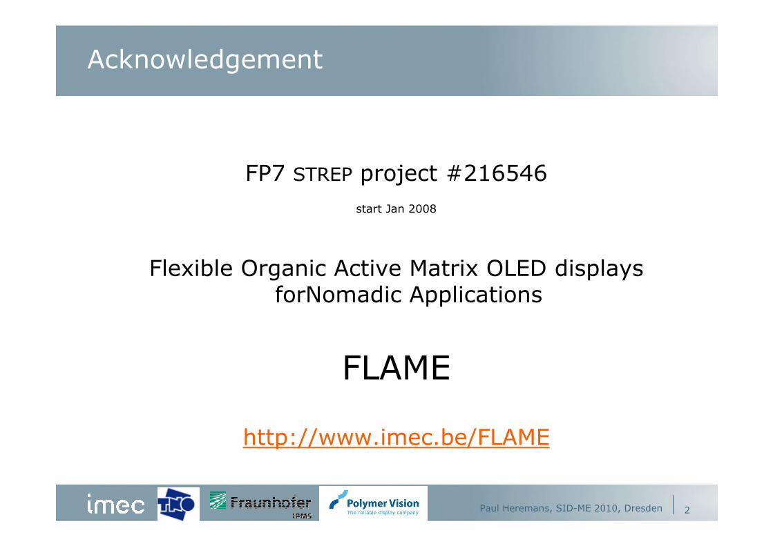
FP7 STREP project #216546
start Jan 2008
Flexible Organic Active Matrix OLED displays forNomadic Applications
FLAME
http://www.imec.be/FLAME
Paul Heremans, SID-ME 2010, Dresden 2
Paul Heremans, SID-ME 2010, Dresden 3
Introduction
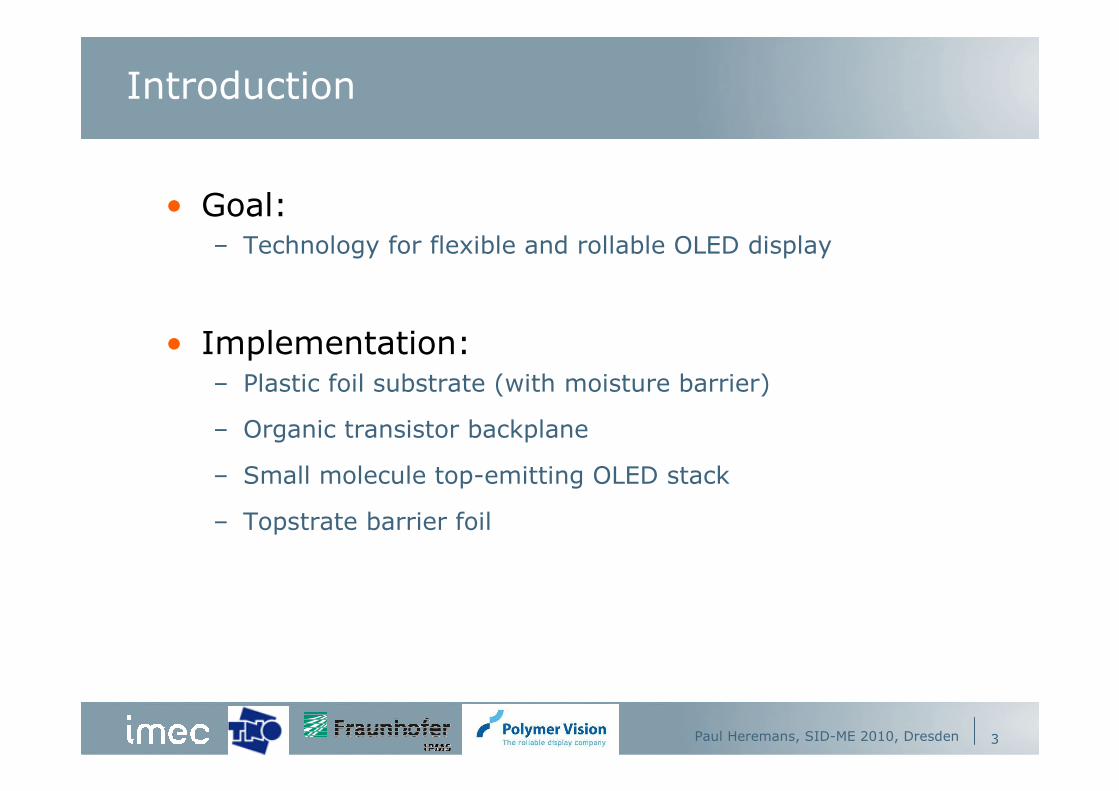
• Goal: – Technology for flexible and rollable OLED display
• Implementation:– Plastic foil substrate (with moisture barrier)
– Organic transistor backplane
– Small molecule top-emitting OLED stack
– Topstrate barrier foil
State of the art
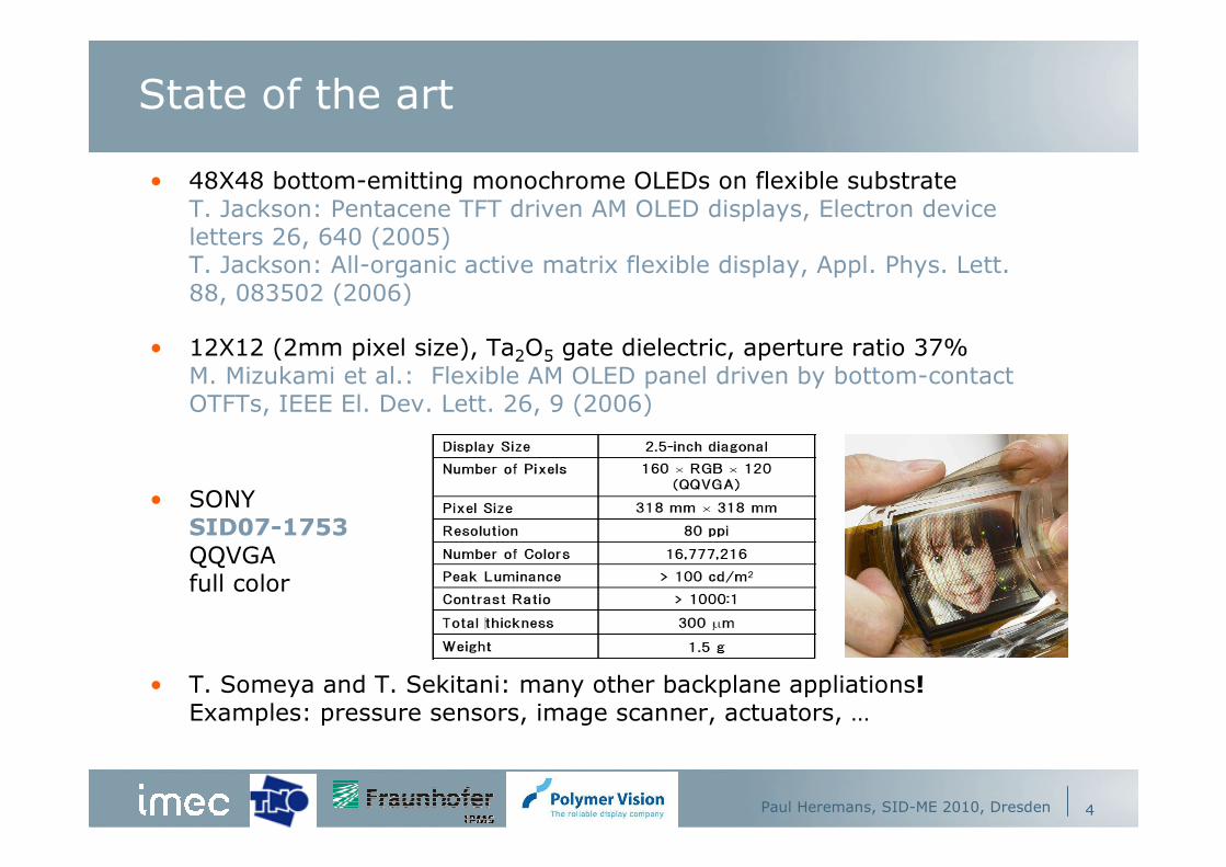
• 48X48 bottom-emitting monochrome OLEDs on flexible substrateT. Jackson: Pentacene TFT driven AM OLED displays, Electron device letters 26, 640 (2005)T. Jackson: All-organic active matrix flexible display, Appl. Phys. Lett. 88, 083502 (2006)
• 12X12 (2mm pixel size), Ta2O5 gate dielectric, aperture ratio 37% M. Mizukami et al.: Flexible AM OLED panel driven by bottom-contact OTFTs, IEEE El. Dev. Lett. 26, 9 (2006)
• SONYSID07-1753QQVGA full color
• T. Someya and T. Sekitani: many other backplane appliations!Examples: pressure sensors, image scanner, actuators, …
Paul Heremans, SID-ME 2010, Dresden 4
Outline
• Backplane
• OLED
• Integration
• Moisture Barrier
Paul Heremans, SID-ME 2010, Dresden 5
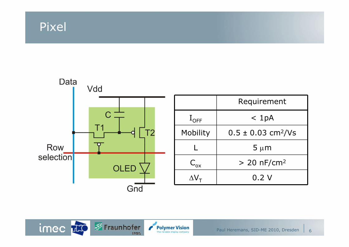
Pixel
< 1pAIOFF
Requirement
Mobility 0.5 ± 0.03 cm2/Vs
L 5 µm
Cox > 20 nF/cm2
∆VT 0.2 V
Paul Heremans, SID-ME 2010, Dresden 6
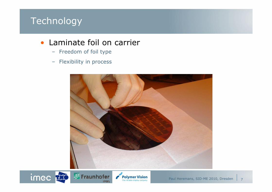
Technology
• Laminate foil on carrier– Freedom of foil type
– Flexibility in process
Paul Heremans, SID-ME 2010, Dresden 7
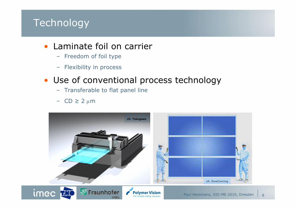
Technology
• Laminate foil on carrier– Freedom of foil type
– Flexibility in process
• Use of conventional process technology– Transferable to flat panel line
– CD ≥ 2 µm
cfr. DowCorning
cfr. Yokogawa
Paul Heremans, SID-ME 2010, Dresden 8
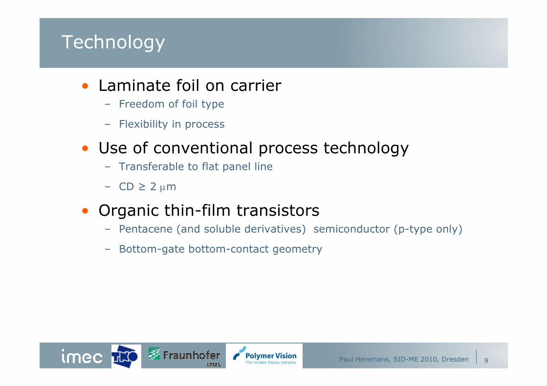
Technology
• Laminate foil on carrier– Freedom of foil type
– Flexibility in process
• Use of conventional process technology– Transferable to flat panel line
– CD ≥ 2 µm
• Organic thin-film transistors– Pentacene (and soluble derivatives) semiconductor (p-type only)
– Bottom-gate bottom-contact geometry
Paul Heremans, SID-ME 2010, Dresden 9
Paul Heremans, SID-ME 2010, Dresden 10
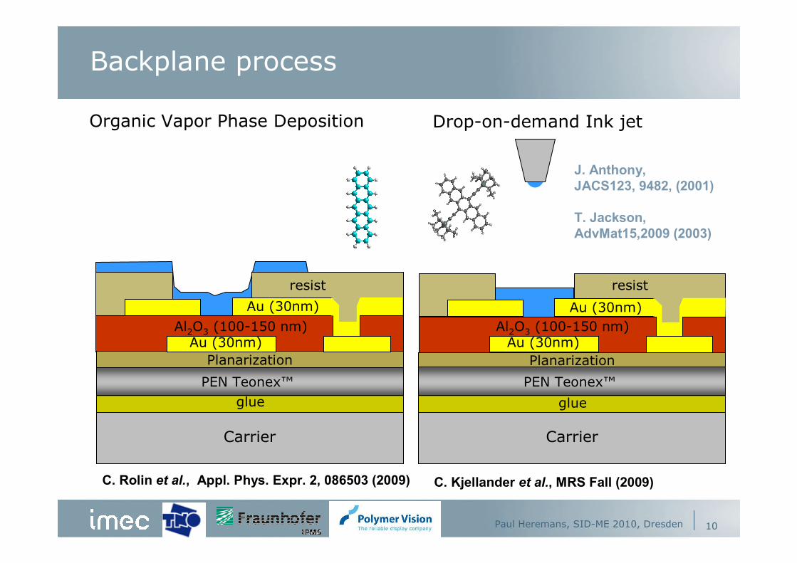
Carrier
glue
PEN Teonex™
Planarization
Au (30nm)
resist
Al2O3 (100-150 nm)
Carrier
glue
PEN Teonex™
Planarization
Au (30nm)
resist
Al2O3 (100-150 nm)
Drop-on-demand Ink jet
Au (30nm) Au (30nm)
Organic Vapor Phase Deposition
C. Rolin et al., Appl. Phys. Expr. 2, 086503 (2009) C. Kjellander et al., MRS Fall (2009)
J. Anthony,
JACS123, 9482, (2001)
T. Jackson,
AdvMat15,2009 (2003)
Backplane process
Performance evaporated pentacene
7
6
5
4
3
2
1
0
Number
1.00.80.60.40.20.0
µ [cm2 / Vs]
µ (AVG) = 0.472 cm2 / Vs
µ (StDev) = 0.0174 cm2 / Vs
3.0
2.5
2.0
1.5
1.0
0.5
0.0
Number
-10 -5 0 5 10VT [V]
VT (AVG) = 0.906096 V
VT (StDev) = 0.496683 V
Paul Heremans, SID-ME 2010, Dresden 11
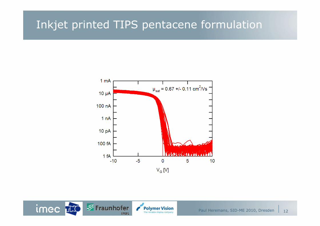
Inkjet printed TIPS pentacene formulation
Paul Heremans, SID-ME 2010, Dresden 12
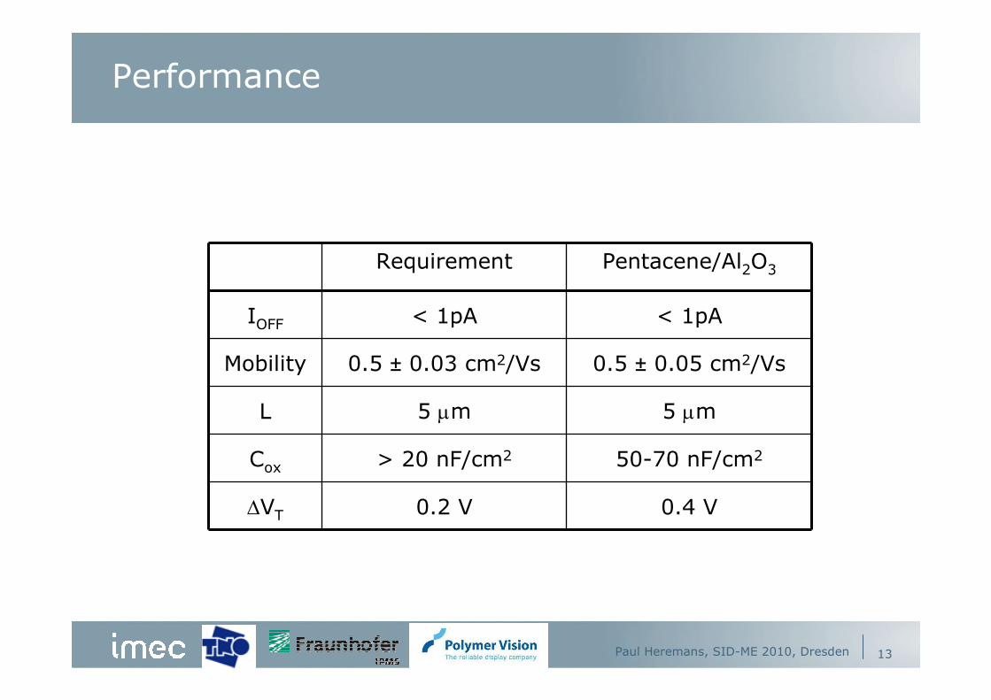
Performance
< 1pA< 1pAIOFF
Requirement Pentacene/Al2O3
Mobility 0.5 ± 0.03 cm2/Vs 0.5 ± 0.05 cm2/Vs
L 5 µm 5 µm
Cox > 20 nF/cm2 50-70 nF/cm2
∆VT 0.2 V 0.4 V
Paul Heremans, SID-ME 2010, Dresden 13
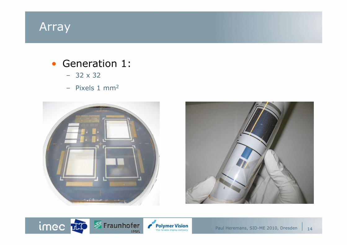
Array
• Generation 1:– 32 x 32
– Pixels 1 mm2
Paul Heremans, SID-ME 2010, Dresden 14
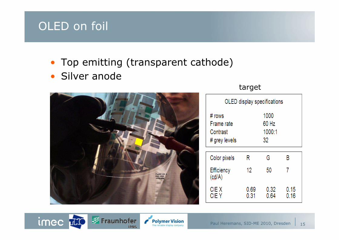
OLED on foil
• Top emitting (transparent cathode)
• Silver anode
Paul Heremans, SID-ME 2010, Dresden 15
target
Transparent cathode
OLED layer stack
interlayer dielectric
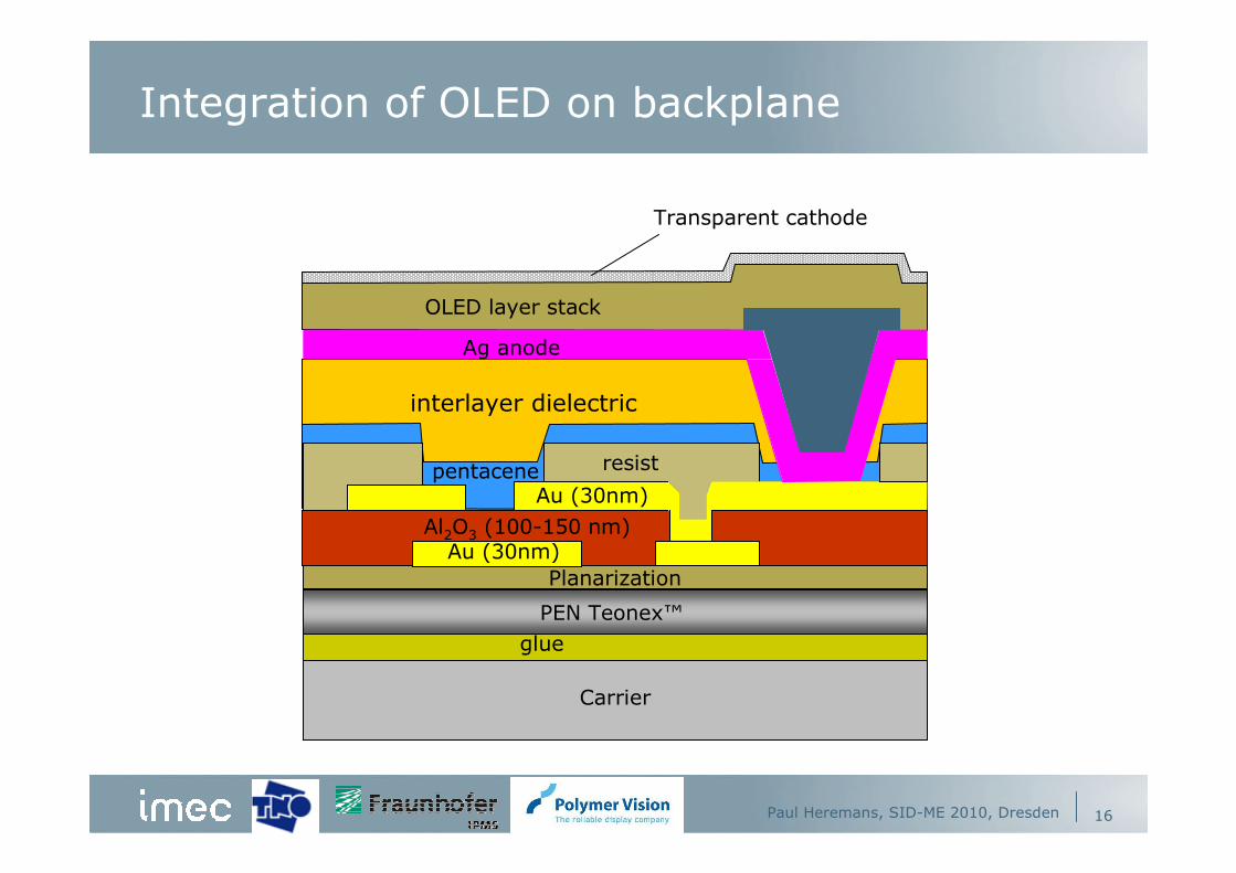
Integration of OLED on backplane
Carrier
glue
PEN Teonex™
Planarization
Au (30nm)
resist
Al2O3 (100-150 nm)
Au (30nm)pentacene
Via hole
Ag anode
Paul Heremans, SID-ME 2010, Dresden 16
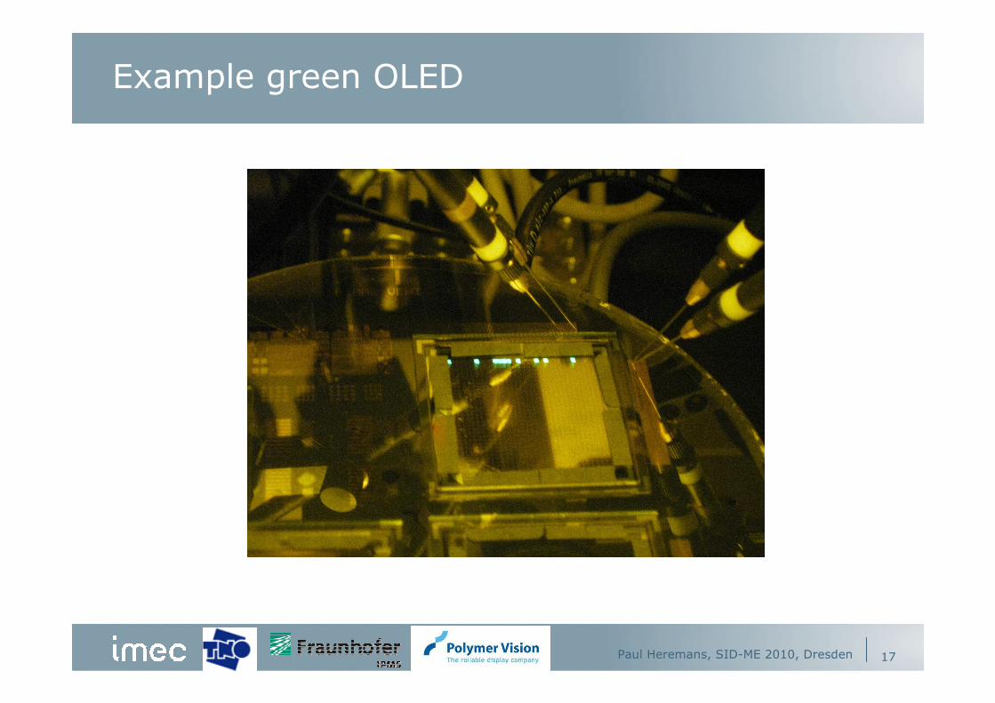
Example green OLED
Paul Heremans, SID-ME 2010, Dresden 17
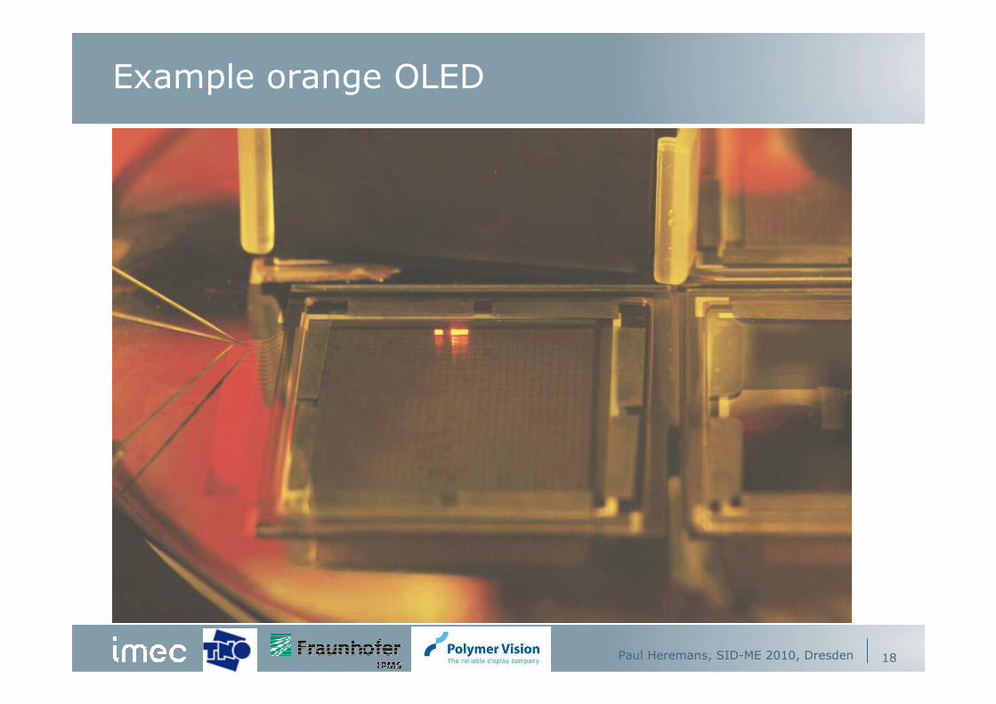
Example orange OLED
Paul Heremans, SID-ME 2010, Dresden 18
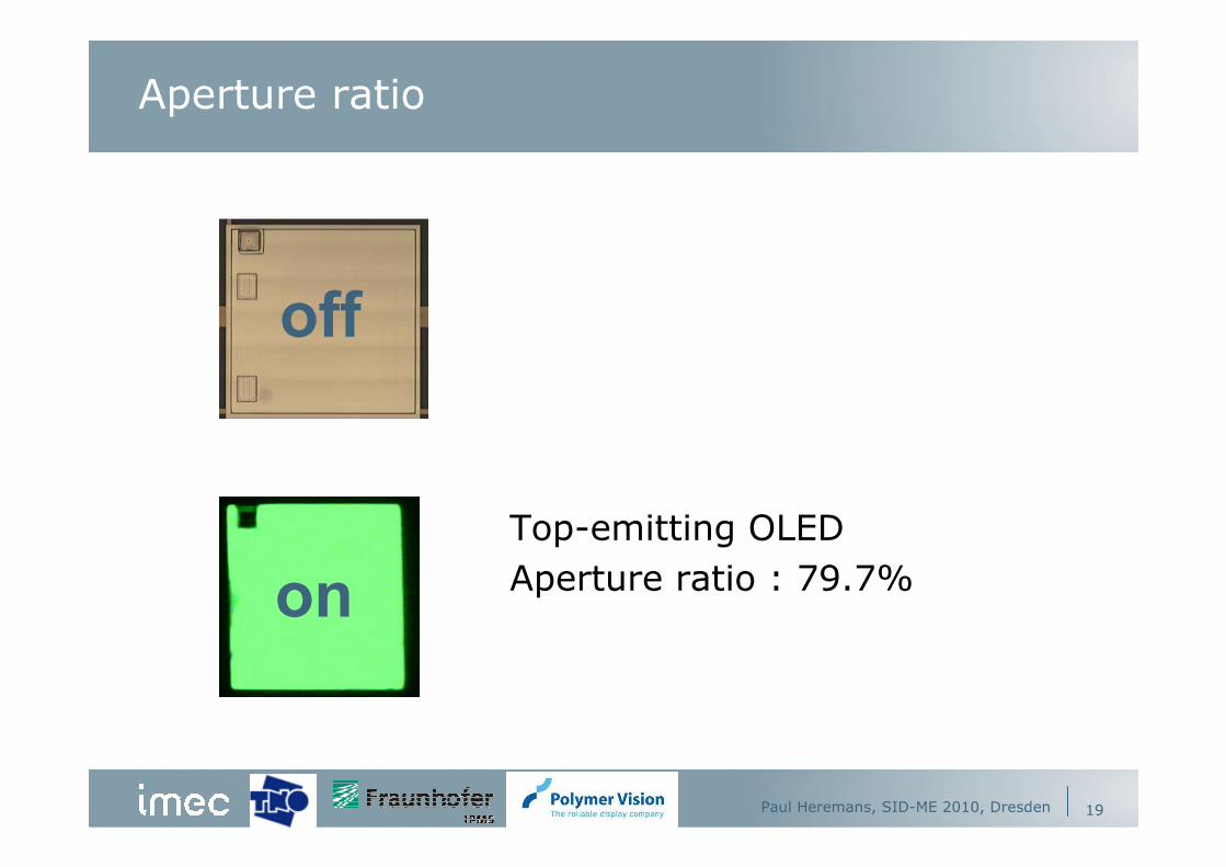
Aperture ratio
Top-emitting OLED
Aperture ratio : 79.7%
off
on
Paul Heremans, SID-ME 2010, Dresden 19
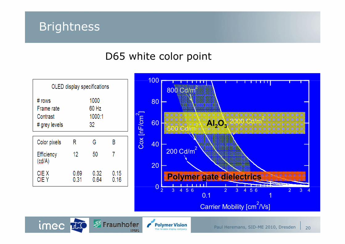
Brightness
D65 white color point
100
80
60
40
20
0
Cox [nF/cm2]
2 3 4 5 6
0.12 3 4 5 6
12 3 4
Carrier Mobility [cm2/Vs]
2000 Cd/m2
500 Cd/m2
200 Cd/m2
800 Cd/m2
Al2O3
Polymer gate dielectrics
Paul Heremans, SID-ME 2010, Dresden 20
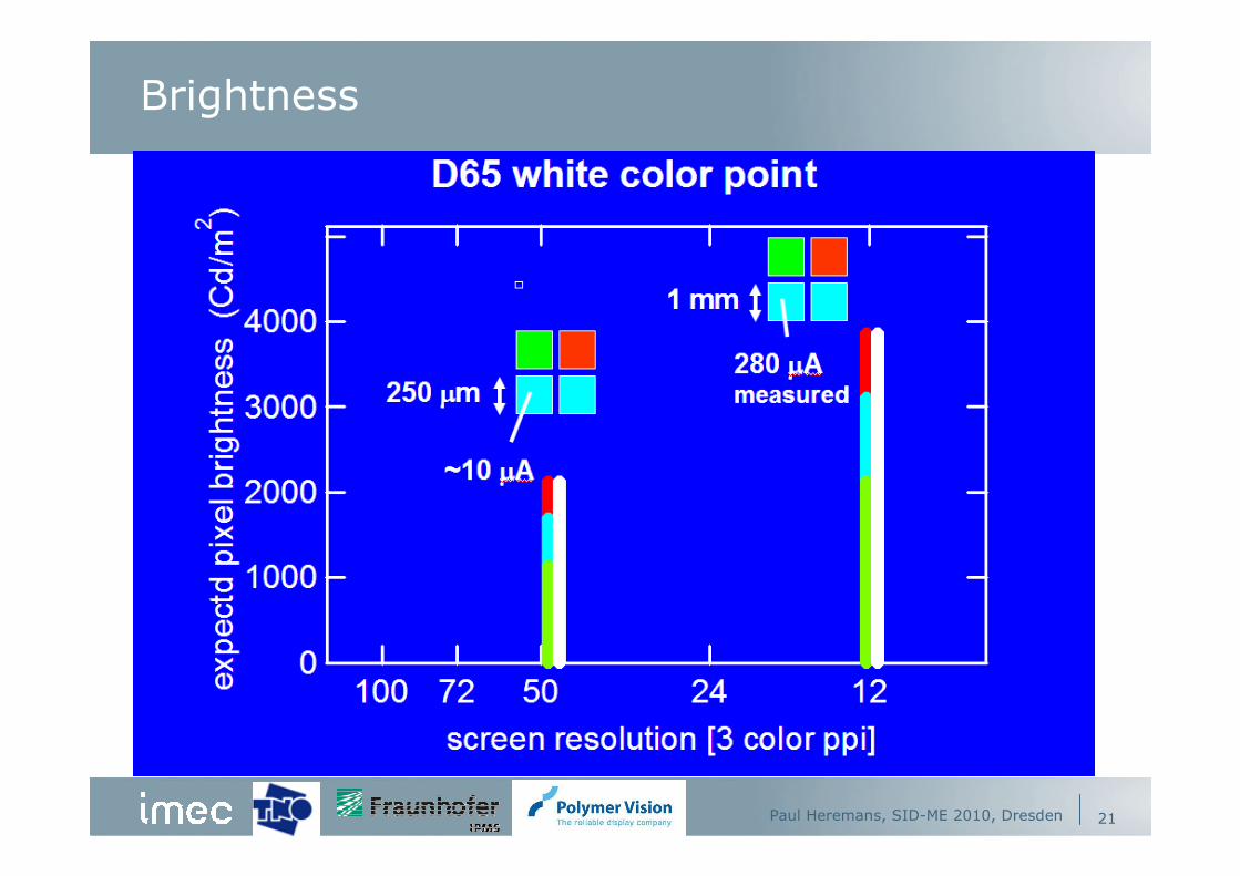
Brightness
Paul Heremans, SID-ME 2010, Dresden 21
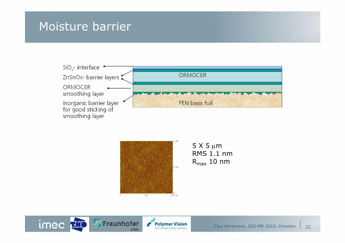
Moisture barrier
Paul Heremans, SID-ME 2010, Dresden 22
5 X 5 µmRMS 1.1 nmRmax 10 nm
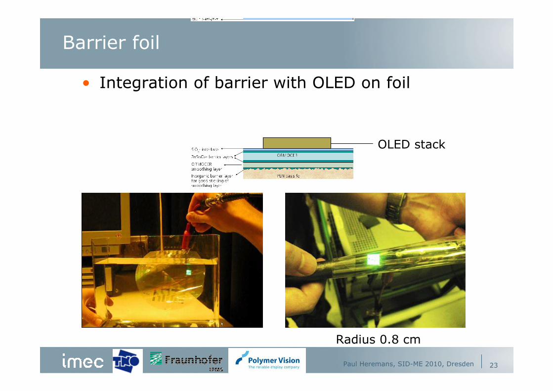
Barrier foil
• Integration of barrier with OLED on foil
Radius 0.8 cm
Paul Heremans, SID-ME 2010, Dresden 23
OLED stack
Summary
• Status :– Pentacene/Al2O3 backplane with green and orange OLEDs integrated
on foil in 32x32 test vehicles
– Moisture barrier with OLEDs integrated on foil and tested for rollability
Paul Heremans, SID-ME 2010, Dresden 24
• Near future :– Integrate row and column drivers
– Develop top-emitting blue OLED pixels on foil
– Apply 3 colors on backplane
– Scale pixel size
– Integrate all in demonstrator
Thank you
Paul Heremans, SID-ME 2010, Dresden 25