Embed Size (px)
Citation preview
Buonassisi (MIT) 2011
Toward a 1D Device Model Part 2: Material Fundamentals
Lecture 8 – 10/4/2011 MIT Fundamentals of Photovoltaics
2.626/2.627 – Fall 2011 Prof. Tonio Buonassisi
1
Buonassisi (MIT) 2011
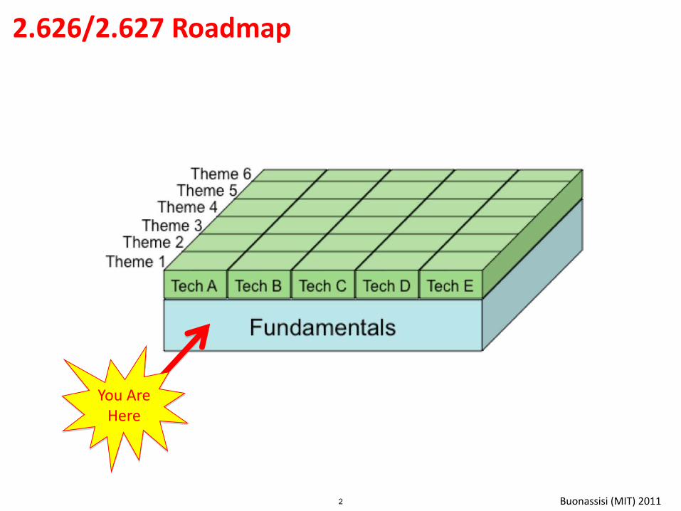
2.626/2.627 Roadmap
You Are Here
2
Buonassisi (MIT) 2011
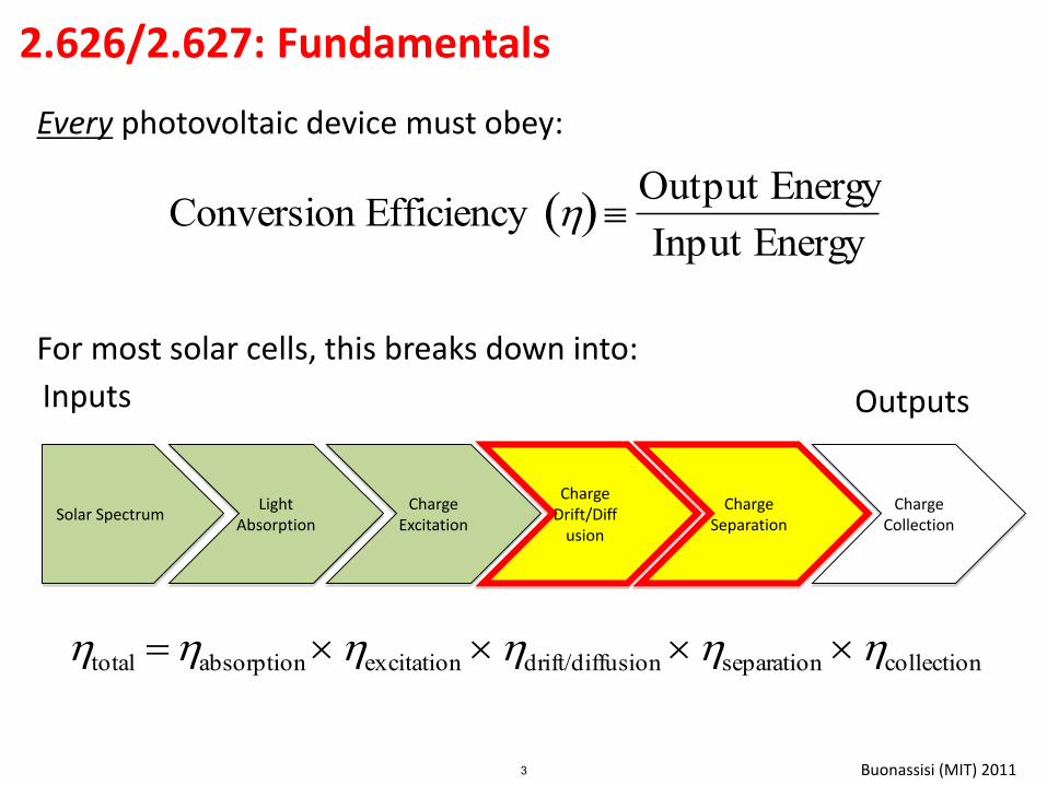
2.626/2.627: Fundamentals
Charge Excitation
Charge Drift/Diff
usion
Charge Separation
Light Absorption
Charge Collection
Outputs
Solar Spectrum
Inputs
Conversion Efficiency Output Energy
Input Energy
Every photovoltaic device must obey:
For most solar cells, this breaks down into:
total absorptionexcitation drift/diffusion separation collection
3
Buonassisi (MIT) 2011
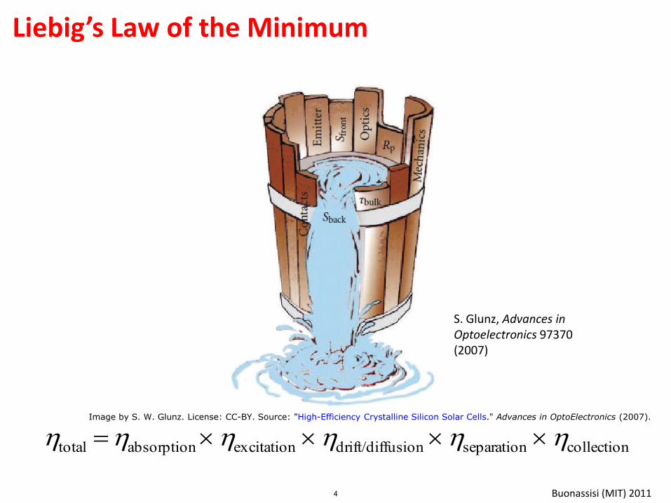
Liebig’s Law of the Minimum
total absorptionexcitation drift/diffusion separation collection
S. Glunz, Advances in Optoelectronics 97370 (2007)
Image by S. W. Glunz. License: CC-BY. Source: "High-Efficiency Crystalline Silicon Solar Cells." Advances in OptoElectronics (2007).
4
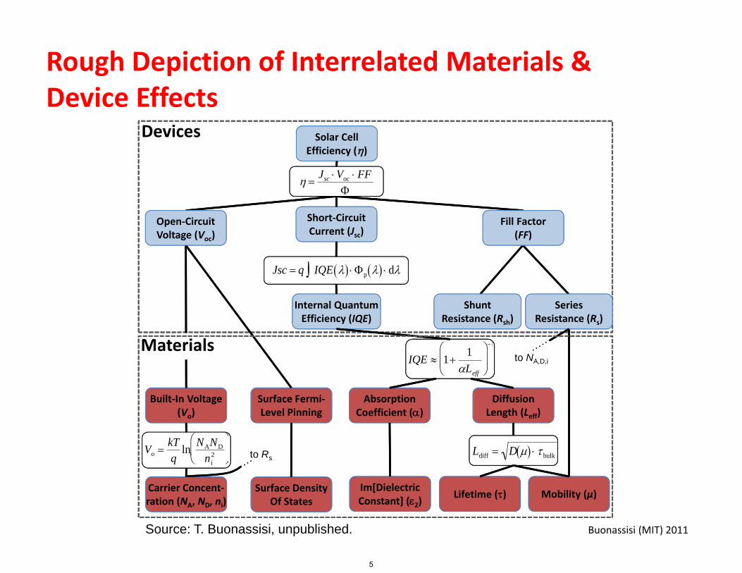
Rough Depiction of Interrelated Materials & Device Effects
Buonassisi (MIT) 2011
Solar Cell Efficiency ()
Short‐Circuit Current (Jsc)
Internal QuantumEfficiency (IQE)
)Carrier Concent‐ration (NA, ND, ni)
AbsorptionCoefficient ()
DiffusionLength (Leff)
Mobility (µ)Lifetime ()
Surface Fermi‐Level Pinning
Built‐In Voltage(Vo)
IQE 1 1Leff
1
Jsc q IQE p d
Ldiff D bulkVo
kTq
ln NAND
ni2
Surface DensityOf States
Im[DielectricConstant] (2)
Devices
Jsc Voc FF
Open‐CircuitVoltage (Voc)
Fill Factor(FF)
Series Resistance (Rs)
ShuntResistance (Rsh)
to Rs
to NA,D,i
Materials
Source: T. Buonassisi, unpublished.
5
Buonassisi (MIT) 2011
1. Describe what minority carrier diffusion length is, and calculate its impact on Jsc, Voc. Describe how minority carrier diffusion length is affected by minority carrier lifetime and minority carrier mobility.
2. Describe how minority carrier diffusion length is measured.
3. Lifetime:
• Describe basic recombination mechanisms in semiconductor materials.
• Calculate excess carrier concentration as a function of carrier lifetime and generation rate. Compare to background (intrinsic + dopant) carrier concentrations.
4. Mobility:
• Describe common mobility-limiting mechanisms (dopants, temperature, ionic semiconductors).
Learning Objectives: Toward a 1D Device Model
6
Buonassisi (MIT) 2011
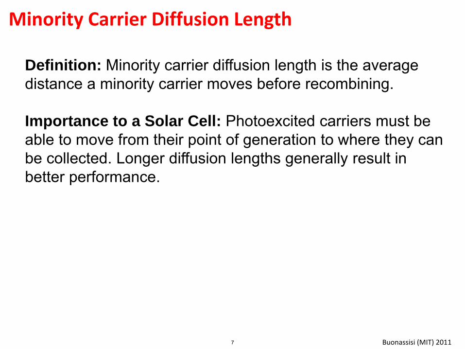
Minority Carrier Diffusion Length
Definition: Minority carrier diffusion length is the average distance a minority carrier moves before recombining. Importance to a Solar Cell: Photoexcited carriers must be able to move from their point of generation to where they can be collected. Longer diffusion lengths generally result in better performance.
7
Buonassisi (MIT) 2011
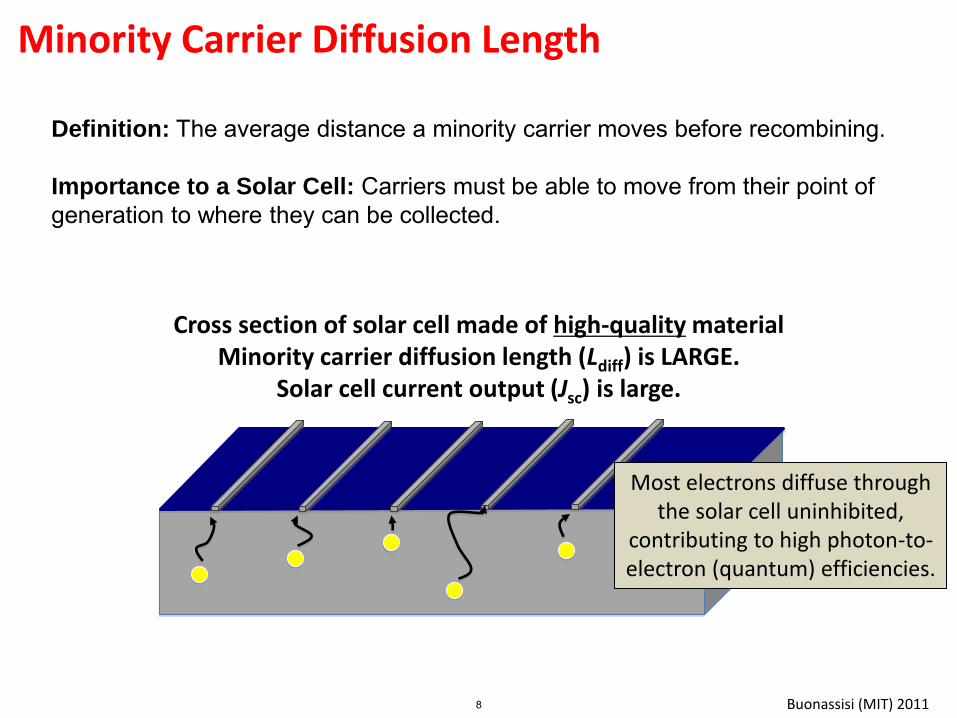
Minority Carrier Diffusion Length
Definition: The average distance a minority carrier moves before recombining. Importance to a Solar Cell: Carriers must be able to move from their point of generation to where they can be collected.
Most electrons diffuse through the solar cell uninhibited,
contributing to high photon-to-electron (quantum) efficiencies.
Cross section of solar cell made of high-quality material Minority carrier diffusion length (Ldiff) is LARGE.
Solar cell current output (Jsc) is large.
8
Buonassisi (MIT) 2011
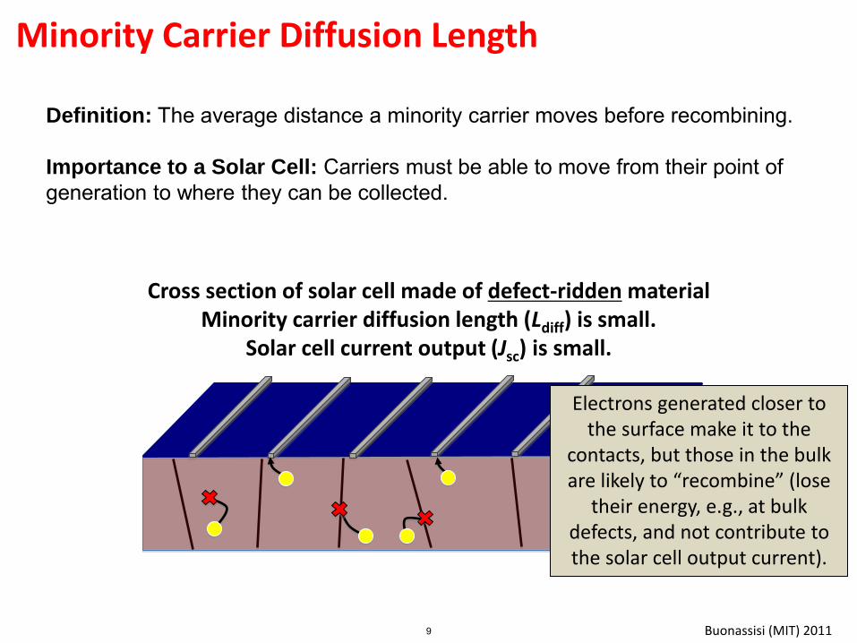
Cross section of solar cell made of defect-ridden material Minority carrier diffusion length (Ldiff) is small.
Solar cell current output (Jsc) is small.
Electrons generated closer to the surface make it to the
contacts, but those in the bulk are likely to “recombine” (lose
their energy, e.g., at bulk defects, and not contribute to the solar cell output current).
Minority Carrier Diffusion Length
Definition: The average distance a minority carrier moves before recombining. Importance to a Solar Cell: Carriers must be able to move from their point of generation to where they can be collected.
9
Buonassisi (MIT) 2011
0
1
2
3
4
5
6
7
8
9
10
0.00 0.10 0.20 0.30 0.40 0.50
Sho
rt C
irct
ui C
urr
en
t [m
A/c
m2
]
Diffusion Length [microns]
PC1D Simulation for 300um thick Si Solar Cell
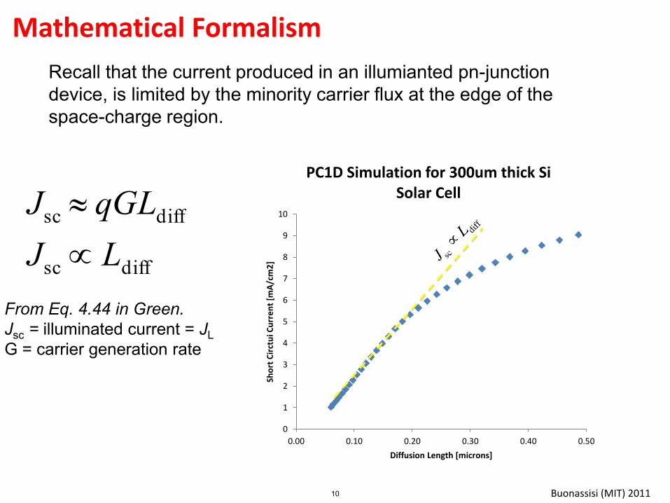
Mathematical Formalism
Recall that the current produced in an illumianted pn-junction device, is limited by the minority carrier flux at the edge of the space-charge region.
Jsc qGLdiff
Jsc Ldiff
From Eq. 4.44 in Green. Jsc = illuminated current = JL G = carrier generation rate
10
Buonassisi (MIT) 2011
Mathematical Formalism
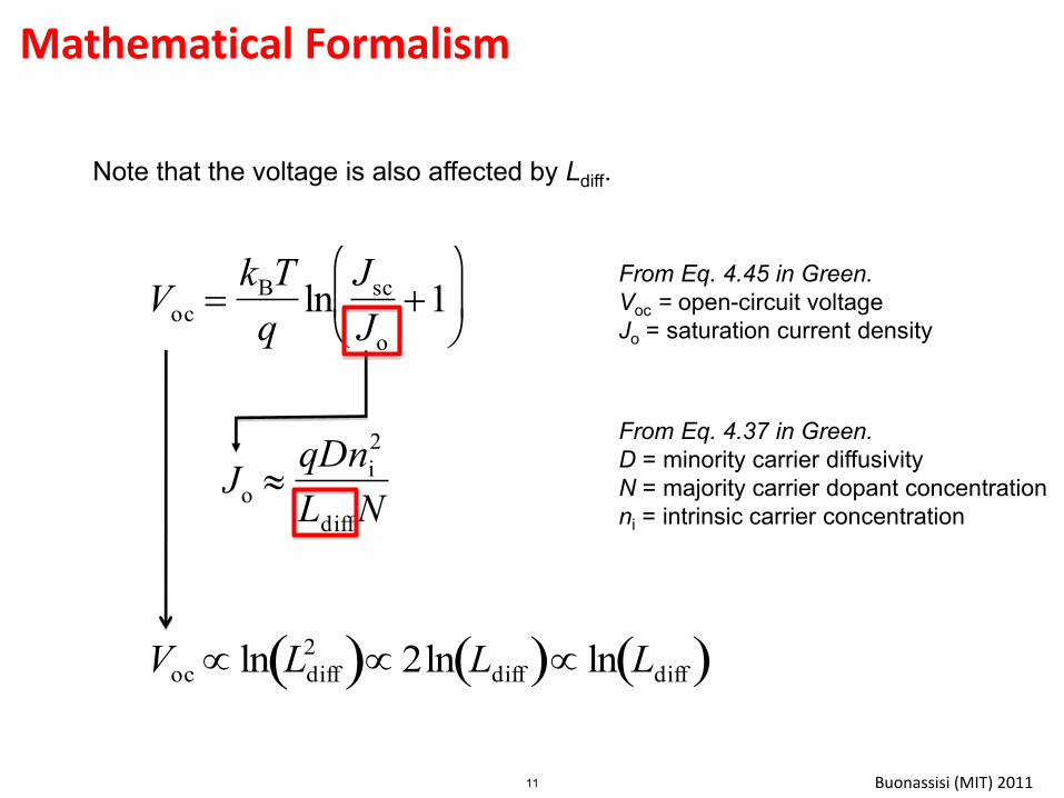
Note that the voltage is also affected by Ldiff.
Voc kBT
qlnJsc
Jo
1
From Eq. 4.45 in Green. Voc = open-circuit voltage Jo = saturation current density
Jo qDni
2
LdiffN
From Eq. 4.37 in Green. D = minority carrier diffusivity N = majority carrier dopant concentration ni = intrinsic carrier concentration
Voc ln Ldiff
2 2ln Ldiff ln Ldiff
11
Buonassisi (MIT) 2011
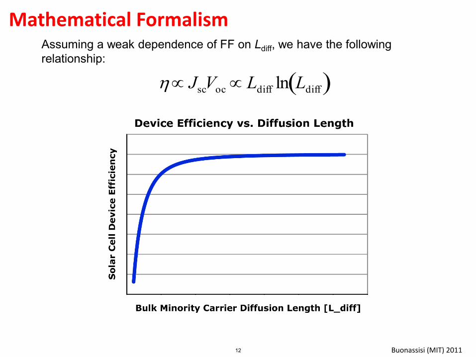
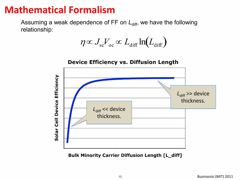
Mathematical Formalism Assuming a weak dependence of FF on Ldiff, we have the following relationship:
JscVoc Ldiff ln Ldiff
12
Buonassisi (MIT) 2011
Mathematical Formalism Assuming a weak dependence of FF on Ldiff, we have the following relationship:
Ldiff << device thickness.
Ldiff >> device thickness.
JscVoc Ldiff ln Ldiff
13
Buonassisi (MIT) 2011
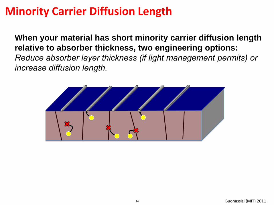
Minority Carrier Diffusion Length
When your material has short minority carrier diffusion length
relative to absorber thickness, two engineering options:
Reduce absorber layer thickness (if light management permits) or increase diffusion length.
14
Buonassisi (MIT) 2011
1. Describe what minority carrier diffusion length is, and calculate its impact on Jsc, Voc. Describe how minority carrier diffusion length is affected by minority carrier lifetime and minority carrier mobility.
2. Describe how minority carrier diffusion length is measured.
3. Lifetime:
• Describe basic recombination mechanisms in semiconductor materials.
• Calculate excess carrier concentration as a function of carrier lifetime and generation rate. Compare to background (intrinsic + dopant) carrier concentrations.
4. Mobility:
• Describe common mobility-limiting mechanisms (dopants, temperature, ionic semiconductors).
Learning Objectives: Toward a 1D Device Model
15
Buonassisi (MIT) 2011
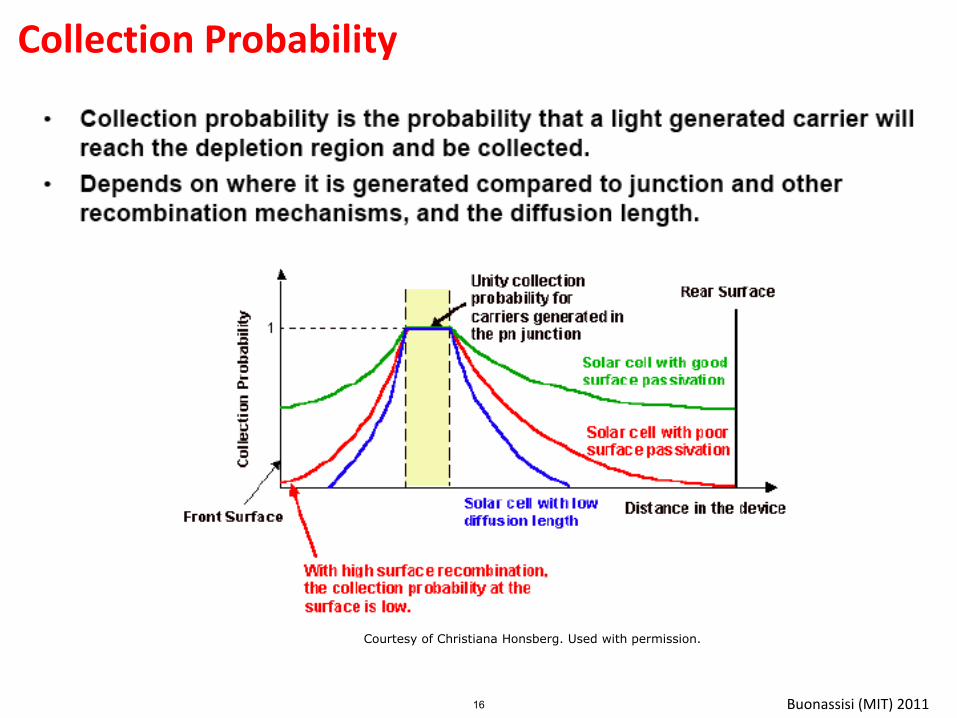
Collection Probability
Courtesy of Christiana Honsberg. Used with permission.
16
Buonassisi (MIT) 2011
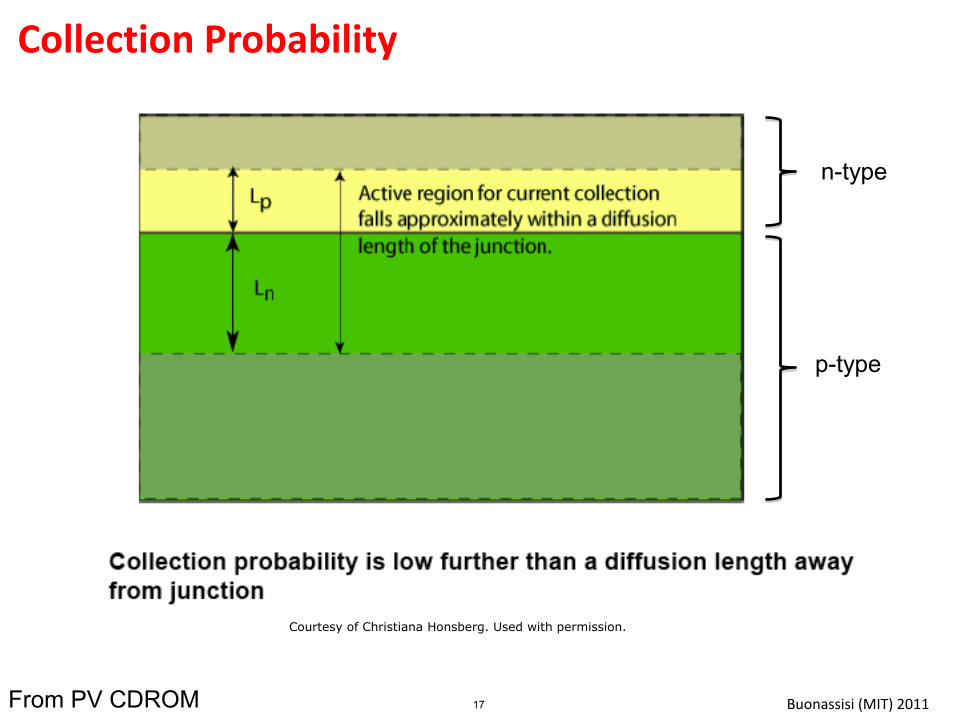
p-type
n-type
Collection Probability
From PV CDROM
Courtesy of Christiana Honsberg. Used with permission.
17
Buonassisi (MIT) 2011
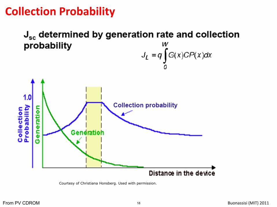
Collection Probability
From PV CDROM
Courtesy of Christiana Honsberg. Used with permission.
18
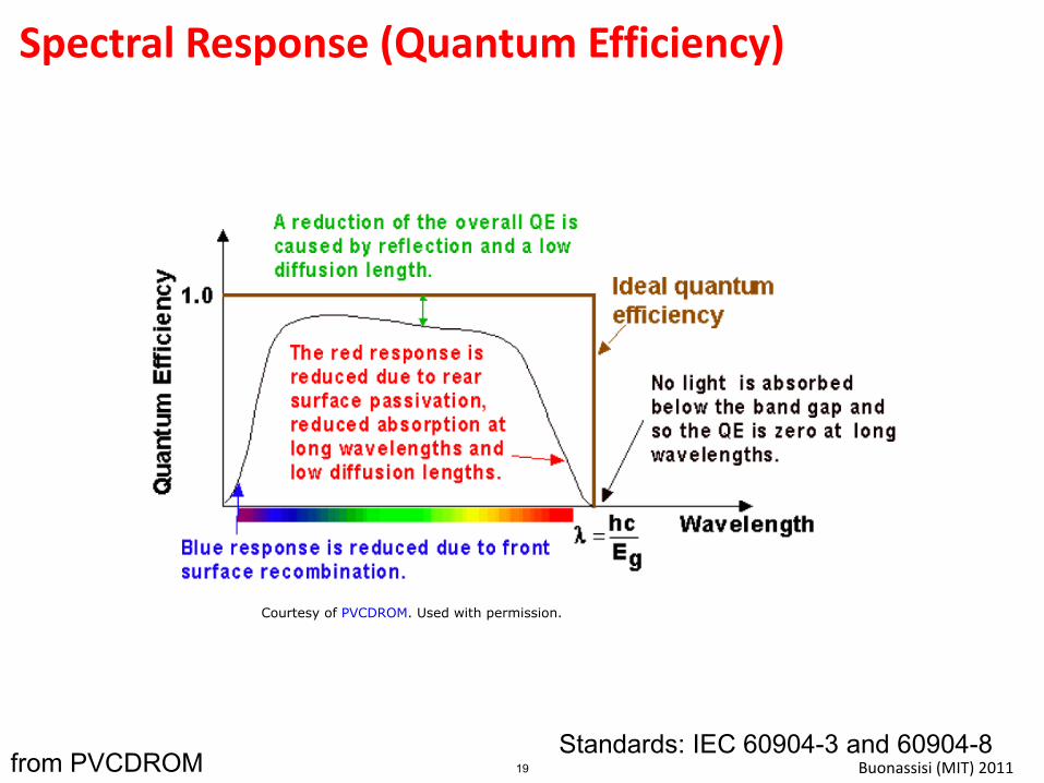
Buonassisi (MIT) 2011 Standards: IEC 60904-3 and 60904-8
from PVCDROM
Spectral Response (Quantum Efficiency)
Courtesy of PVCDROM. Used with permission.
19
Buonassisi (MIT) 2011
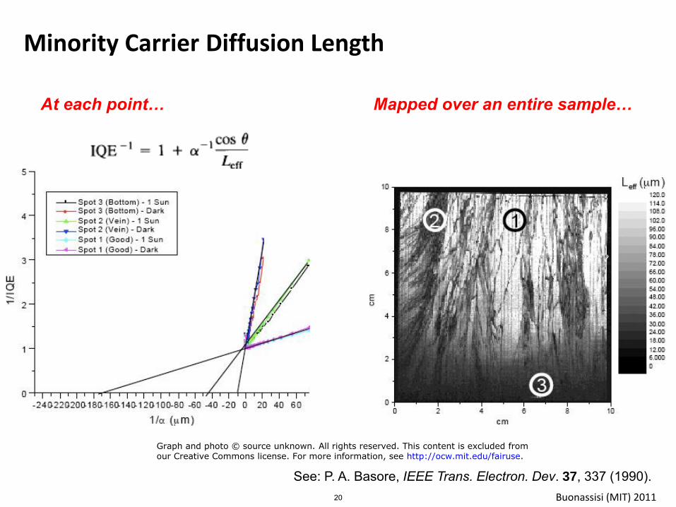
Minority Carrier Diffusion Length
See: P. A. Basore, IEEE Trans. Electron. Dev. 37, 337 (1990).
At each point… Mapped over an entire sample…
Graph and photo © source unknown. All rights reserved. This content is excluded fromour Creative Commons license. For more information, see http://ocw.mit.edu/fairuse.
20
Buonassisi (MIT) 2011
What Limits Diffusion Length?
21
Buonassisi (MIT) 2011
What Limits the Minority Carrier Diffusion Length?
Quick answer: Recombination-active defects, intrinsic mobility limitations, or absence of percolation pathways.
R.B. Bergmann, Appl. Phys. A 69, 187 (1999)
Thin films: Effect of bulk defects (GBs) on . Nanostructured: Effect of morphology on .
F. Yang et al., ACS Nano 2, 1022 (2008)
Please see lecture video for visuals.
22
Buonassisi (MIT) 2011
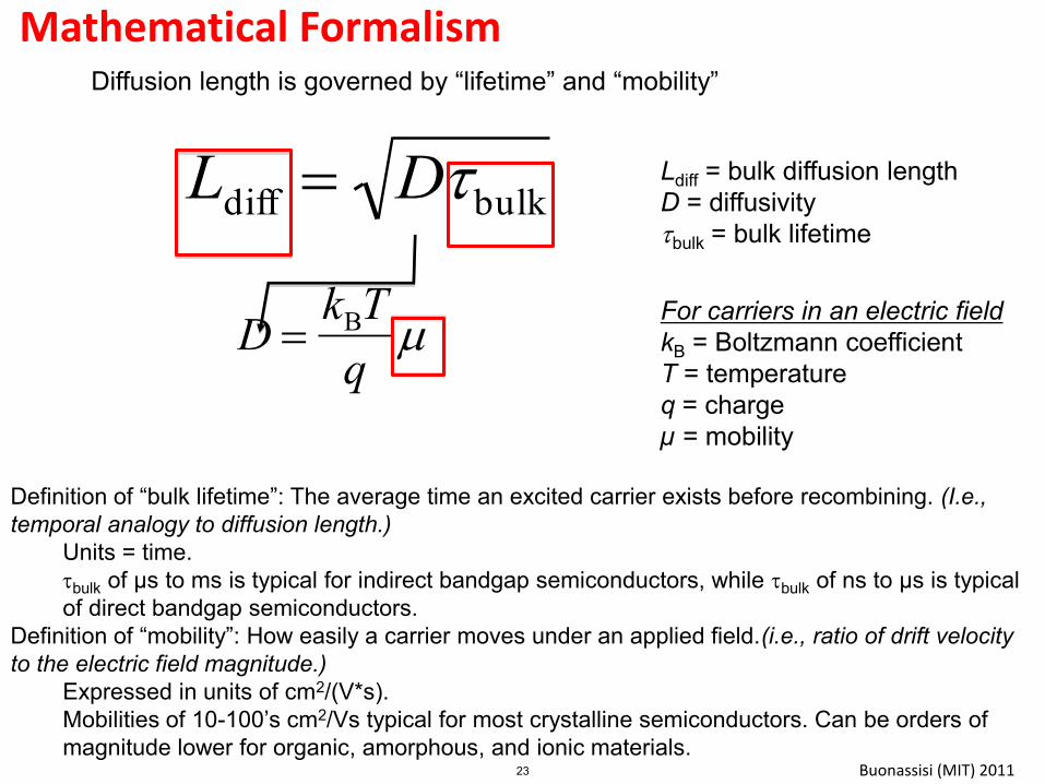
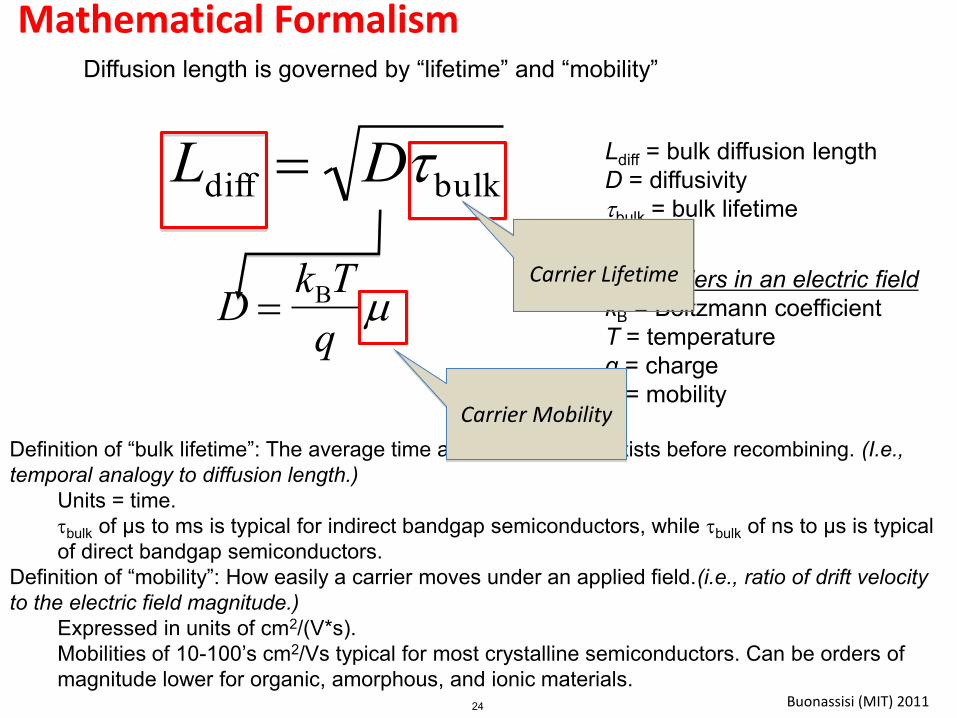
Ldiff DtbulkLdiff = bulk diffusion length D = diffusivity tbulk = bulk lifetime
D kBT
q
For carriers in an electric field kB = Boltzmann coefficient T = temperature q = charge µ = mobility
Mathematical Formalism Diffusion length is governed by “lifetime” and “mobility”
Definition of “bulk lifetime”: The average time an excited carrier exists before recombining. (I.e., temporal analogy to diffusion length.)
Units = time. tbulk of µs to ms is typical for indirect bandgap semiconductors, while tbulk of ns to µs is typical of direct bandgap semiconductors.
Definition of “mobility”: How easily a carrier moves under an applied field.(i.e., ratio of drift velocity to the electric field magnitude.)
Expressed in units of cm2/(V*s). Mobilities of 10-100’s cm2/Vs typical for most crystalline semiconductors. Can be orders of magnitude lower for organic, amorphous, and ionic materials.
23
Buonassisi (MIT) 2011
Ldiff DtbulkLdiff = bulk diffusion length D = diffusivity tbulk = bulk lifetime
D kBT
q
For carriers in an electric field kB = Boltzmann coefficient T = temperature q = charge µ = mobility
Mathematical Formalism Diffusion length is governed by “lifetime” and “mobility”
Definition of “bulk lifetime”: The average time an excited carrier exists before recombining. (I.e., temporal analogy to diffusion length.)
Units = time. tbulk of µs to ms is typical for indirect bandgap semiconductors, while tbulk of ns to µs is typical of direct bandgap semiconductors.
Definition of “mobility”: How easily a carrier moves under an applied field.(i.e., ratio of drift velocity to the electric field magnitude.)
Expressed in units of cm2/(V*s). Mobilities of 10-100’s cm2/Vs typical for most crystalline semiconductors. Can be orders of magnitude lower for organic, amorphous, and ionic materials.
Carrier Mobility
Carrier Lifetime
24
Buonassisi (MIT) 2011
1. Describe what minority carrier diffusion length is, and calculate its impact on Jsc, Voc. Describe how minority carrier diffusion length is affected by minority carrier lifetime and minority carrier mobility.
2. Describe how minority carrier diffusion length is measured.
3. Lifetime:
• Describe basic recombination mechanisms in semiconductor materials.
• Calculate excess carrier concentration as a function of carrier lifetime and generation rate. Compare to background (intrinsic + dopant) carrier concentrations.
4. Mobility:
• Describe common mobility-limiting mechanisms (dopants, temperature, ionic semiconductors).
Learning Objectives: Toward a 1D Device Model
25
Buonassisi (MIT) 2011
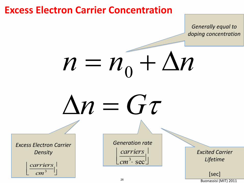
Excess Electron Carrier Concentration
n n0 n
n Gt
Excited Carrier Lifetime
[sec]
Excess Electron Carrier Density
carriers
cm 3
Generation rate
carriers
cm3 sec
Generally equal to doping concentration
26
Buonassisi (MIT) 2011
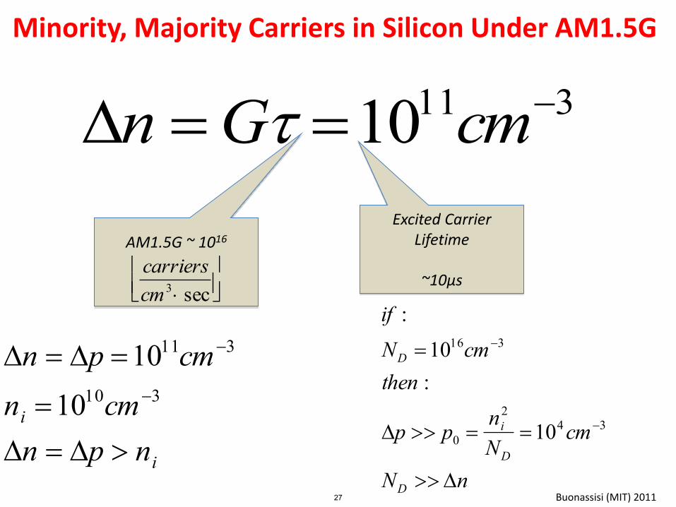
Minority, Majority Carriers in Silicon Under AM1.5G
n Gt 1011cm3
Excited Carrier Lifetime
~10μs
AM1.5G ~ 1016
carriers
cm3 sec
n p 1011cm3
ni 1010cm3
n p ni
if :
ND 1016cm 3
then :
p p0 ni
2
ND104cm 3
ND n27
Buonassisi (MIT) 2011
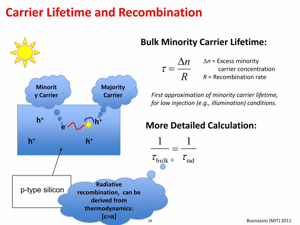
Carrier Lifetime and Recombination
e- h+
h+
h+
h+
Minority Carrier
Majority Carrier
1
tbulk
1
trad
More Detailed Calculation:
p-type silicon
Bulk Minority Carrier Lifetime:
t n
R
n = Excess minority carrier concentration R = Recombination rate
First approximation of minority carrier lifetime, for low injection (e.g., illumination) conditions.
Radiative recombination, can be
derived from thermodynamics:
[ε=α] 28
Buonassisi (MIT) 2011
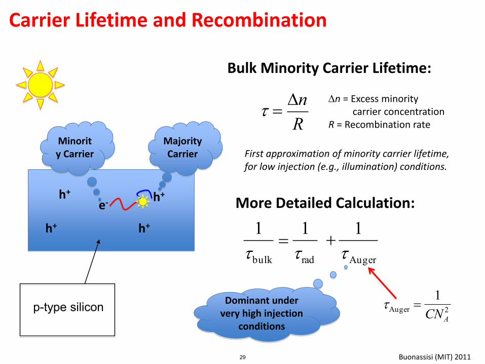
Carrier Lifetime and Recombination
e- h+
h+
h+
h+
Minority Carrier
Majority Carrier
1
tAuger
1
tbulk
1
trad
More Detailed Calculation:
Dominant under very high injection
conditions
tAuger 1
CNA2p-type silicon
Bulk Minority Carrier Lifetime:
t n
R
n = Excess minority carrier concentration R = Recombination rate
First approximation of minority carrier lifetime, for low injection (e.g., illumination) conditions.
29
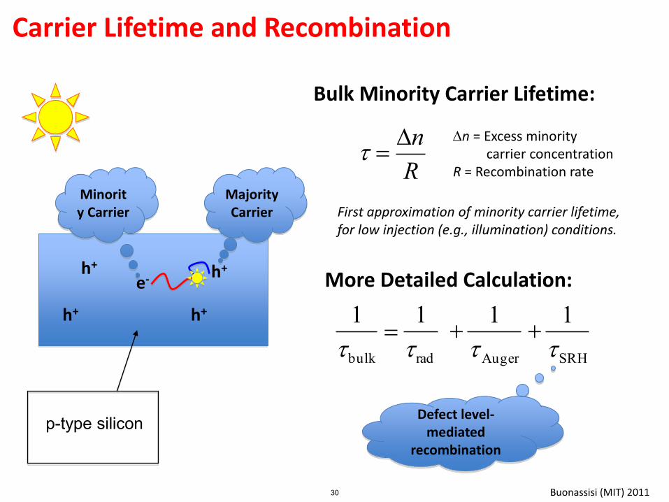
Buonassisi (MIT) 2011
Carrier Lifetime and Recombination
e- h+
h+
h+
h+
Minority Carrier
Majority Carrier
1
tAuger
1
tbulk
1
trad
More Detailed Calculation:
1
tSRH
Defect level-mediated
recombination
p-type silicon
Bulk Minority Carrier Lifetime:
t n
R
n = Excess minority carrier concentration R = Recombination rate
First approximation of minority carrier lifetime, for low injection (e.g., illumination) conditions.
30
Buonassisi (MIT) 2011
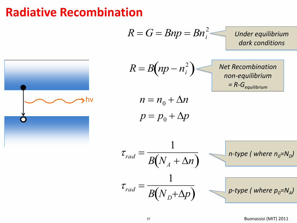
hν n n0 n
p p0 p
Radiative Recombination
Net Recombination non-equilibrium
= R-Gequilibrium
R B np ni2
Under equilibrium dark conditions
R G Bnp Bni2
n-type ( where n0=ND)
p-type ( where p0=NA)
trad 1
B NA n
trad 1
B NDp
31
Buonassisi (MIT) 2011
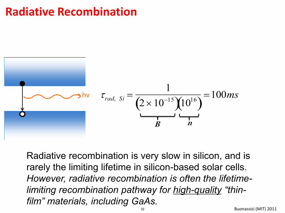
hν
Radiative Recombination
Radiative recombination is very slow in silicon, and is rarely the limiting lifetime in silicon-based solar cells. However, radiative recombination is often the lifetime-limiting recombination pathway for high-quality “thin-film” materials, including GaAs.
trad, Si 1
2 1015 1016 100ms
B n
32
Buonassisi (MIT) 2011
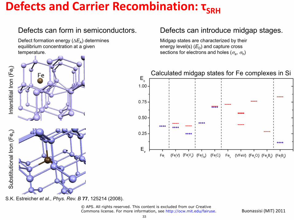
Defects and Carrier Recombination: τSRH
Defects can form in semiconductors. Defect formation energy (EA) determines equilibrium concentration at a given temperature.
Inte
rstit
ial I
ron
(Fe i
) S
ubst
itutio
nal I
ron
(Fe s
)
Defects can introduce midgap stages. Midgap states are characterized by their energy level(s) (ED) and capture cross sections for electrons and holes (se, sh)
S.K. Estreicher et al., Phys. Rev. B 77, 125214 (2008).
Calculated midgap states for Fe complexes in Si
© APS. All rights reserved. This content is excluded from our CreativeCommons license. For more information, see http://ocw.mit.edu/fairuse.
33
Buonassisi (MIT) 2011
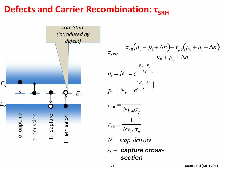
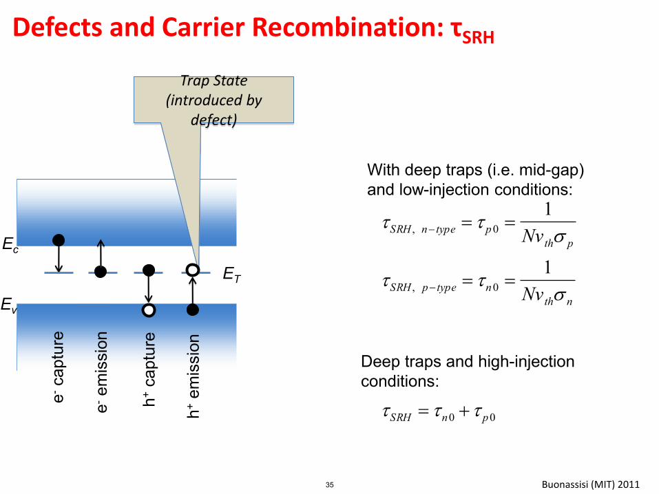
Defects and Carrier Recombination: τSRH
tSRH tn0 n0 p1 n t p0 p0 n1 n
n0 p0 n
n1 Nc e
ET Ec
kT
p1 Nv e
Ev ET
kT
t p0 1
Nv ths p
tn0 1
Nv ths n
N trap density
s
Ec
Ev
ET
capture cross-section
Trap State (introduced by
defect)
e- c
aptu
re
e- e
mis
sion
h+ c
aptu
re
h+ e
mis
sion
34
Buonassisi (MIT) 2011
Defects and Carrier Recombination: τSRH
tSRH , n type t p0 1
Nv ths p
tSRH , p type tn0 1
Nv ths n
tSRH tn0 t p0
Ec
Ev
ET
Trap State (introduced by
defect)
e- c
aptu
re
e- e
mis
sion
h+ c
aptu
re
h+ e
mis
sion
With deep traps (i.e. mid-gap) and low-injection conditions:
Deep traps and high-injection conditions:
35
Buonassisi (MIT) 2011
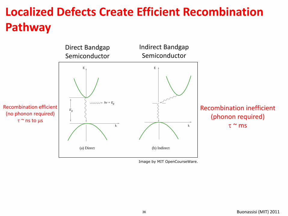
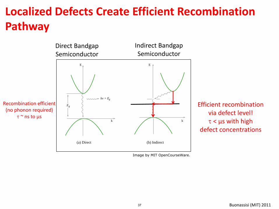
Localized Defects Create Efficient Recombination Pathway
Direct Bandgap Semiconductor
Indirect Bandgap Semiconductor
Recombination inefficient (phonon required)
t ~ ms
Recombination efficient (no phonon required)
t ~ ns to µs
36
Eg
E E
k k
(a) Direct (b) Indirect
hv = Eg
Image by MIT OpenCourseWare.
Buonassisi (MIT) 2011
Direct Bandgap Semiconductor
Indirect Bandgap Semiconductor
Efficient recombination via defect level! t < µs with high
defect concentrations
Recombination efficient(no phonon required)
t ~ ns to µs
Localized Defects Create Efficient Recombination Pathway
37
Eg
E E
k k
(a) Direct (b) Indirect
hv = Eg
Image by MIT OpenCourseWare.
Buonassisi (MIT) 2011
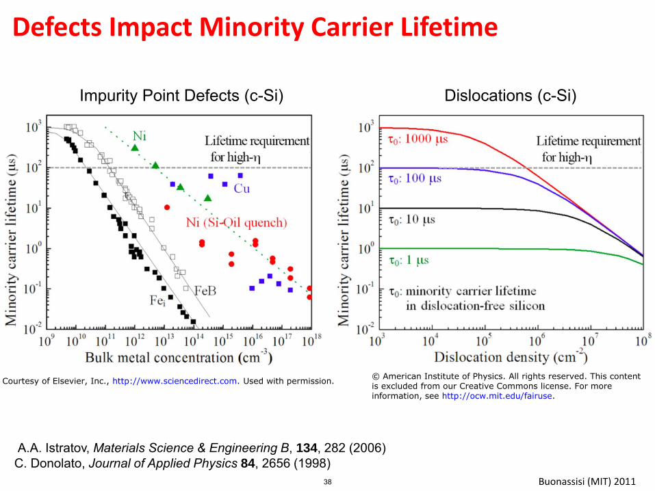
Defects Impact Minority Carrier Lifetime
Dislocations (c-Si)
C. Donolato, Journal of Applied Physics 84, 2656 (1998) A.A. Istratov, Materials Science & Engineering B, 134, 282 (2006)
Impurity Point Defects (c-Si)
Courtesy of Elsevier, Inc., http://www.sciencedirect.com. Used with permission.© American Institute of Physics. All rights reserved. This contentis excluded from our Creative Commons license. For moreinformation, see http://ocw.mit.edu/fairuse.
38
Buonassisi (MIT) 2011
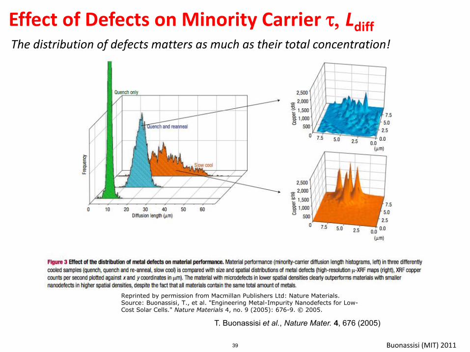
Effect of Defects on Minority Carrier t, Ldiff
T. Buonassisi et al., Nature Mater. 4, 676 (2005)
The distribution of defects matters as much as their total concentration!
Reprinted by permission from Macmillan Publishers Ltd: Nature Materials.Source: Buonassisi, T., et al. "Engineering Metal-Impurity Nanodefects for Low-Cost Solar Cells." Nature Materials 4, no. 9 (2005): 676-9. © 2005.
39
Buonassisi (MIT) 2011
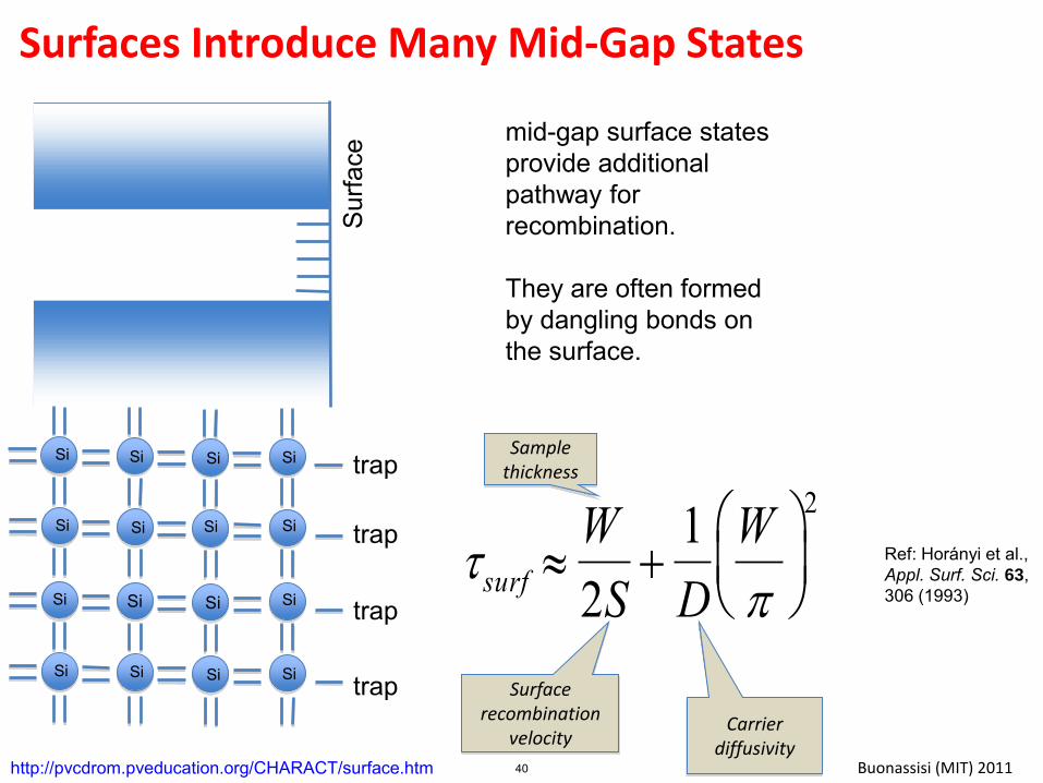
Surfaces Introduce Many Mid-Gap States
Sur
face
mid-gap surface states provide additional pathway for recombination. They are often formed by dangling bonds on the surface.
Si
Si
Si
Si
Si
Si
Si
Si
Si
Si
Si
Si
Si
Si
Si
Si
trap
trap
trap
trap
tsurf W
2S
1
D
W
2
http://pvcdrom.pveducation.org/CHARACT/surface.htm
Sample thickness
Surface recombination
velocity
Carrier diffusivity
Ref: Horányi et al., Appl. Surf. Sci. 63, 306 (1993)
40
Buonassisi (MIT) 2011
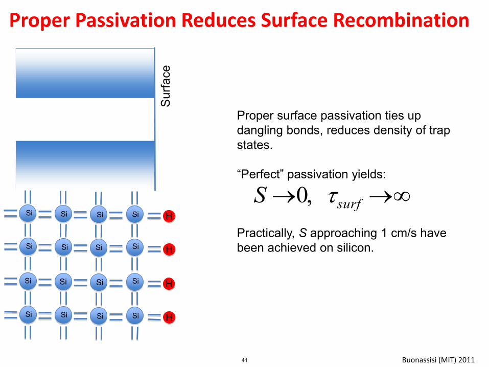
Proper Passivation Reduces Surface Recombination
Sur
face
Proper surface passivation ties up dangling bonds, reduces density of trap states. “Perfect” passivation yields: Practically, S approaching 1 cm/s have been achieved on silicon.
Si
Si
Si
Si
Si
Si
Si
Si
Si
Si
Si
Si
Si
Si
Si
Si
H
H
H
H
S0, tsurf
41
Buonassisi (MIT) 2011
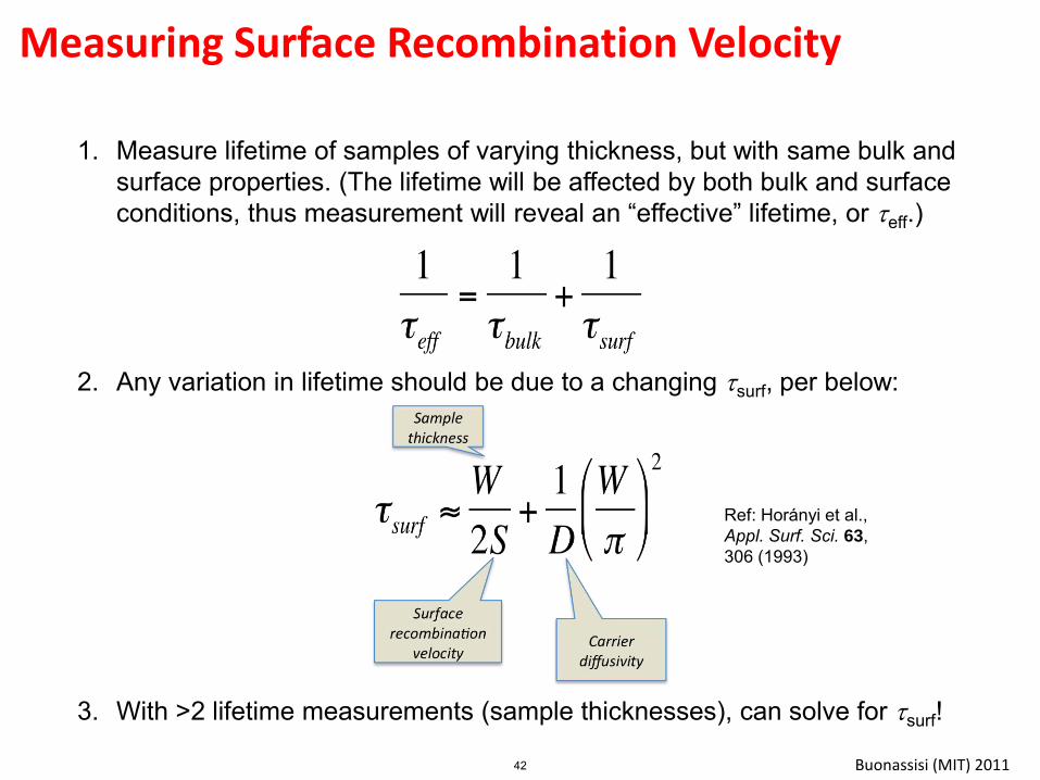
Measuring Surface Recombination Velocity
Ref: Horányi et al., Appl. Surf. Sci. 63, 306 (1993)
1. Measure lifetime of samples of varying thickness, but with same bulk and surface properties. (The lifetime will be affected by both bulk and surface conditions, thus measurement will reveal an “effective” lifetime, or teff.)
2. Any variation in lifetime should be due to a changing tsurf, per below:
3. With >2 lifetime measurements (sample thicknesses), can solve for tsurf!
42
Buonassisi (MIT) 2011
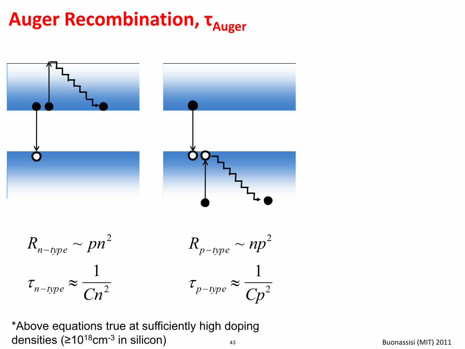
Rn type ~ pn2
tn type 1
Cn2
Rp type ~ np2
t p type 1
Cp2
Auger Recombination, τAuger
*Above equations true at sufficiently high doping densities (≥1018cm-3 in silicon) 43
Buonassisi (MIT) 2011
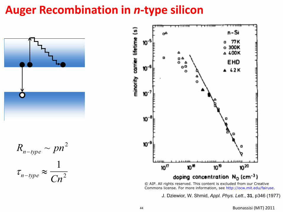
Auger Recombination in n-type silicon
J. Dziewior, W. Shmid, Appl. Phys. Lett., 31, p346 (1977)
Rn type ~ pn2
tn type 1
Cn2
© AIP. All rights reserved. This content is excluded from our CreativeCommons license. For more information, see http://ocw.mit.edu/fairuse.
44
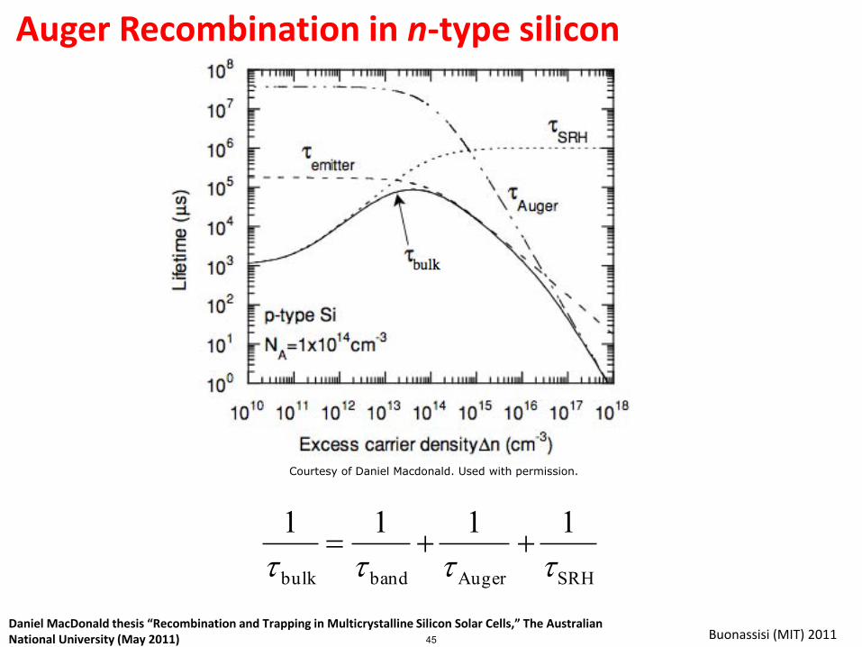
Buonassisi (MIT) 2011 Daniel MacDonald thesis “Recombination and Trapping in Multicrystalline Silicon Solar Cells,” The Australian National University (May 2011)
1
tAuger
1
t bulk
1
t band
1
tSRH
Auger Recombination in n-type silicon
Courtesy of Daniel Macdonald. Used with permission.
45
Buonassisi (MIT) 2011
Measuring Minority Carrier Lifetime
1
tAuger
1
tbulk
1
trad
1
tSRH
Recall that
If defect-mitigated recombination is dominant, band-to-band radiative recombination will be suppressed: In fact, band-to-band (radiative recombination) and defect-mitigated (non-radiative recombination) are inversely proportional. By imaging the band-to-band (radiative) recombination using a very sensitive CCD camera, we are able to quantitatively extract the minority carrier lifetime.
1
trad
1
tSRH
or
trad tSRH
46
Buonassisi (MIT) 2011
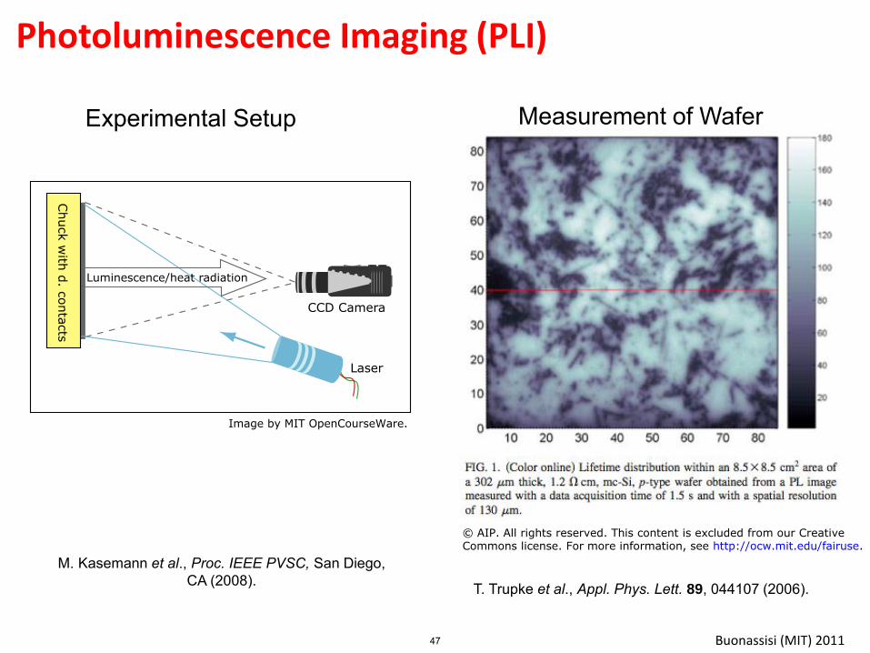
Photoluminescence Imaging (PLI)
T. Trupke et al., Appl. Phys. Lett. 89, 044107 (2006).
M. Kasemann et al., Proc. IEEE PVSC, San Diego, CA (2008).
Experimental Setup Measurement of Wafer
© AIP. All rights reserved. This content is excluded from our CreativeCommons license. For more information, see http://ocw.mit.edu/fairuse.
47
Laser
CCD Camera
Chuck w
ith d. contacts
Luminescence/heat radiation
Image by MIT OpenCourseWare.
Buonassisi (MIT) 2011
S. Rein, Lifetime spectroscopy. Springer-Verlag (Berlin, 2005). p. 430
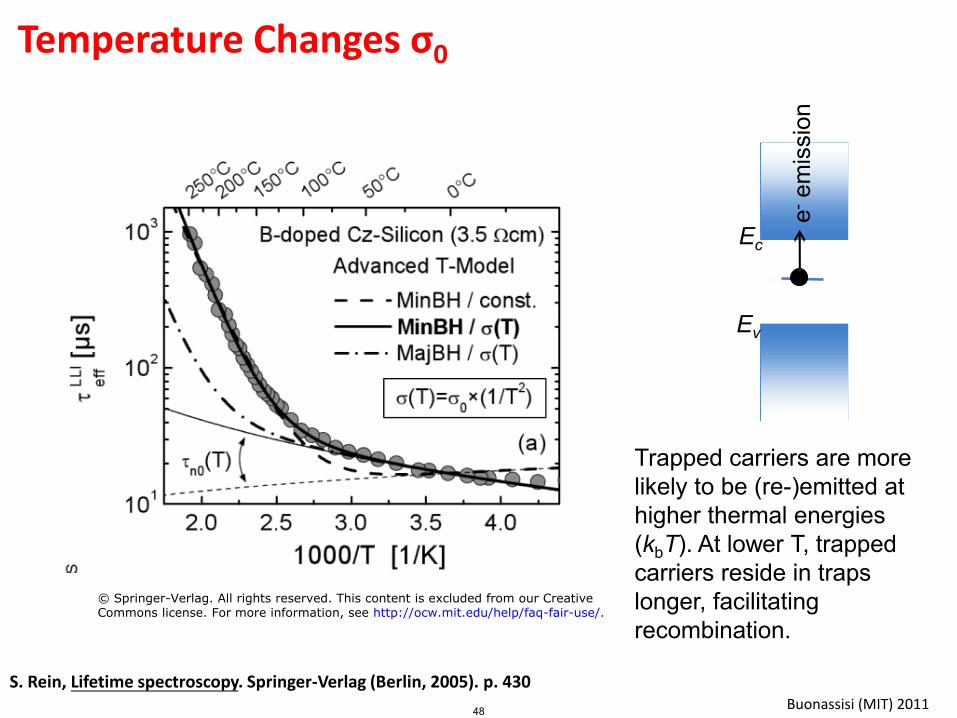
Temperature Changes σ0
Ec
Ev
e- e
mis
sion
Trapped carriers are more likely to be (re-)emitted at higher thermal energies (kbT). At lower T, trapped carriers reside in traps longer, facilitating recombination.
© Springer-Verlag. All rights reserved. This content is excluded from our CreativeCommons license. For more information, see http://ocw.mit.edu/help/faq-fair-use/.
48
Buonassisi (MIT) 2011
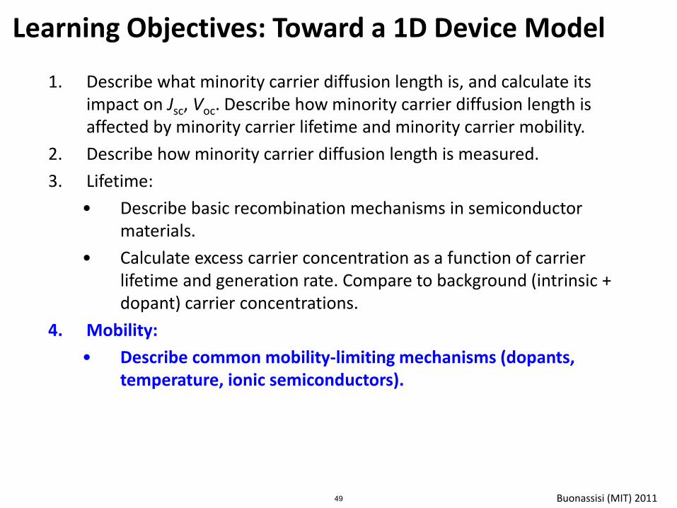
1. Describe what minority carrier diffusion length is, and calculate its impact on Jsc, Voc. Describe how minority carrier diffusion length is affected by minority carrier lifetime and minority carrier mobility.
2. Describe how minority carrier diffusion length is measured.
3. Lifetime:
• Describe basic recombination mechanisms in semiconductor materials.
• Calculate excess carrier concentration as a function of carrier lifetime and generation rate. Compare to background (intrinsic + dopant) carrier concentrations.
4. Mobility:
• Describe common mobility-limiting mechanisms (dopants, temperature, ionic semiconductors).
Learning Objectives: Toward a 1D Device Model
49
Buonassisi (MIT) 2011
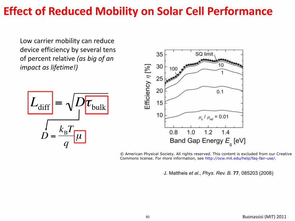
J. Mattheis et al., Phys. Rev. B. 77, 085203 (2008)
Effect of Reduced Mobility on Solar Cell Performance
Low carrier mobility can reduce device efficiency by several tens of percent relative (as big of an impact as lifetime!)
© American Physical Society. All rights reserved. This content is excluded from our CreativeCommons license. For more information, see http://ocw.mit.edu/help/faq-fair-use/.
50
Buonassisi (MIT) 2011
What Limits Mobility?
1. Defect Scattering 2. Trapping at stretched bonds 3. Incomplete percolation pathways 4. Phonon Scattering
F. Yang et al., ACS Nano 2, 1022 (2008)
Example of complex percolation pathway Example of carrier trapping
L. Wagner et al., PRL 101, 265501 (2008)
Diagrams removed due to copyright restrictions. See lecture video.
51
Buonassisi (MIT) 2011
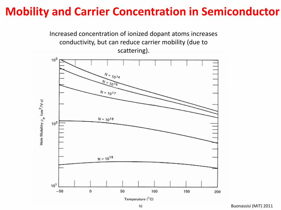
Mobility and Carrier Concentration in Semiconductor
Increased concentration of ionized dopant atoms increases conductivity, but can reduce carrier mobility (due to
scattering).
52
Buonassisi (MIT) 2011
F. Yang et al., ACS Nano 2, 1022 (2008)
Percolation Pathways
Both µ and t play a role in determining Ldiff, and hence efficiency, for various device architectures.
Table removed due to copyright restrictions.See lecture video.
53
Buonassisi (MIT) 2011
Simple Example
1. Well-behaved inorganic semiconductor (no effect of trapping at stretched bonds and incomplete percolation pathways).
2. Defect scattering dominant ionized dopants inside sample scatter carriers.
54
Buonassisi (MIT) 2011
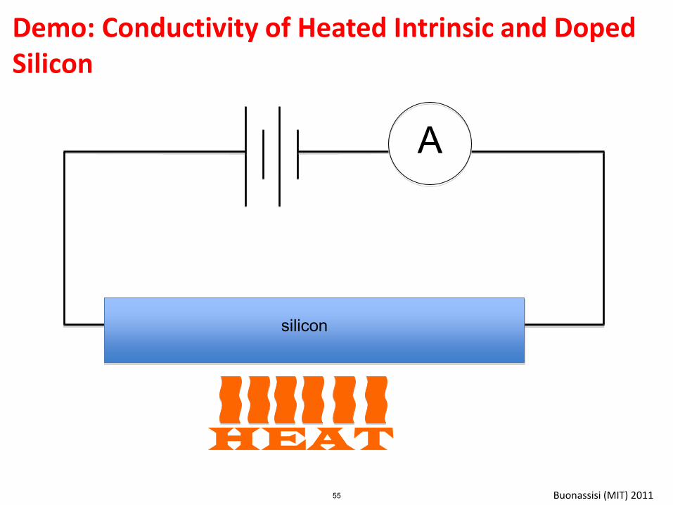
silicon
A
HEAT
Demo: Conductivity of Heated Intrinsic and Doped Silicon
55
Buonassisi (MIT) 2011
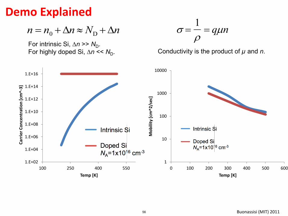
Demo Explained
1.E+02
1.E+04
1.E+06
1.E+08
1.E+10
1.E+12
1.E+14
1.E+16
100 250 400 550
Car
rier
Co
nce
ntr
atio
n [
cm^
-3]
Temp [K]
"IntrinsicCarriers"
"Carriers DopedNa=1e16"
1
10
100
1000
10000
0 100 200 300 400 500 600
Mo
bili
ty [
cm^2
/sec
]
Temp [K]
n n0 n ND n
For intrinsic Si, n >> ND. For highly doped Si, n << ND.
s 1
qn
Conductivity is the product of µ and n.
56
MIT OpenCourseWarehttp://ocw.mit.edu
2.627 / 2.626 Fundamentals of PhotovoltaicsFall 2013
For information about citing these materials or our Terms of Use, visit: http://ocw.mit.edu/terms.