Embed Size (px)
Citation preview

TB67H400AHG
2016-12-22
1 ©2016 TOSHIBA CORPORATION
TOSHIBA BiCD Integrated Circuit Silicon Monolithic
TB67H400AHG PWM Chopper-Type Brushed DC Motor driver The TB67H400AHG is brushed DC motor driver of a PWM chopper-type. The TB67H400AHG is a dual channel H-SW driver which can control two brushed DC motors. Moreover, the parallel control function (Large mode) of an output part is built in, and 1ch high current drive is also possible. Fabricated with the BiCD process, the TB67H400AHG is rated at 50 V, 4.0 A (2ch)/8.0 A (1ch). Features Monolithic motor driver using BiCD process. Capable of controlling two brushed DC motor. 2 drive modes (PWM controlled constant current/ direct PWM) 4 operation modes (Clock-wise/Counter clock-wise/Brake/Stop (Off)) Low on-resistance output stage (High side+Low side:0.49 Ω (typ.)) High voltage and current (for specification, please refer to absolute
maximum ratings and operating ranges.) Built-in error detection circuits (Thermal shutdown (TSD), over-current
detection (ISD), and power-on reset (POR)). The VCC regulator for internal circuit operation is built in. Able to customize PWM (internal chopping) frequency by external
components. Note: Please be careful about the thermal conditions during use.
HZIP25-P-1.00F Weight: 7.6 g (typ.)
TB67H400AHG
2016-12-22
2
Pin assignment Top view
VR
EF
VC
C
GN
D
PW
MB
OS
CM
INA
2
OU
TA+
INB
2
GN
D
OU
TB+
OU
TA-
OU
TB-
VM
NC
NC
HB
MO
DE
INA
1
PW
MA
INB
1
TBLK
AB
RS
A
GN
D
GN
D
GN
D
RS
B

TB67H400AHG
2016-12-22
3
Block diagram Please note that in the block diagram, functional blocks or constants may be omitted or simplified for explanatory purposes.
INB1
INB2
TBLKAB
PWMB
PWMA
VREF
Motor Oscillator
OSCM
VCC Regulator
VCC
TSD
ISD RSB
Motor Control Logic
Predriver RSA
VM
Current Reference
Setting
Current Comp
Current Comp
Predriver
Current Level Set
Power-on Reset
OSC-Clock Converter
System Oscillator
GND
INA2
INA1
Standby Control
+ Blank time Selector
+ H-Bridge
Mode select +
Signal Decode Logic
HBMODE
H-bridge H-bridge

TB67H400AHG
2016-12-22
4
Notes: All the grounding wires of the TB67H400AHG must run on the solder mask of the PCB. It must also be externally terminated at a single point. Also, the grounding method should be considered for efficient heat dissipation. Careful attention should be paid to the layout of the output, VM and GND traces, to avoid short circuits across output pins or to the power supply or ground. If such a short circuit occurs, the device may be permanently damaged. Also, the utmost care should be taken for pattern designing and implementation of the device since it has power supply pins (VM, RS, OUT, and GND) through which a particularly large current may run. If these pins are wired incorrectly, an operation error may occur or the device may be destroyed. The logic input pins must also be wired correctly. Otherwise, the device may be damaged owing to a current running through the IC that is larger than the specified current. Careful attention should be paid to design patterns and mountings.

TB67H400AHG
2016-12-22
5
Pin description TB67H400AHG (HZIP25) Pin No.1-25
Pin No. Pin name Function
1 VCC Internal regulator voltage monitor pin 2 NC Non connection
3 GND Ground pin
4 NC Non connection
5 VREF Motor output current setting pin
6 HBMODE H-Bridge operation mode setting pin
7 OSCM Oscillator frequency setting pin
8 INA1 Motor Ach IN1 signal input pin
9 INA2 Motor Ach IN2 signal input pin
10 PWMA Motor Ach short brake signal input pin
11 PWMB Motor Bch short brake signal input pin
12 INB1 Motor Bch IN1 signal input pin
13 INB2 Motor Bch IN2 signal input pin
14 TBLKAB Motor Ach and Bch Digital tBLK setting pin
15 GND Ground pin
16 RSA Motor Ach output current sense pin
17 OUTA+ Motor Ach+ output pin
18 GND Ground pin
19 OUTA- Motor Ach- output pin
20 GND Ground pin
21 OUTB- Motor Bch- output pin
22 GND Ground pin
23 OUTB+ Motor Bch+ output pin
24 RSB Motor Bch output current sense pin
25 VM Motor Voltage supply pin
Please do not connect any pattern to the NC pin.

TB67H400AHG
2016-12-22
6
INPUT/OUTPUT Equivalent circuit Pin name Input/Output signal Equivalent circuit INA1 INA2 PWMA INB1 INB2 PWMB TBLKAB HBMODE
Digital input (VIH/VIL) VIH: 2.0 V (min) to 5.5 V (max) VIL: 0 V (min) to 0.8 V (max)
VCC VREF
VCC regulator specification 4.75 V (min) to 5.0 V (typ.) to 5.25 V (max) VREF input voltage range 0 V to 4.0 V
OSCM
OSCM setup frequency 0.64 MHz (min) to 1.12 MHz (typ.) to 2.4 MHz (max)
OUTA+ OUTA- OUTB+ OUTB- RSA RSB
VM operation range 10 V (min) to 47 V (max) OUTPUT pin voltage range 10 V (min) to 47 V (max)
Please note that in the equivalent input circuit, functional blocks or constants may be omitted or simplified for explanatory purposes.
100k
Ω
1kΩ
GND
Logic Input
1kΩ
VCC
GND
VREF
500Ω
1kΩ OSCM
GND
GND
RS
OUT+ OUT-
TB67H400AHG
2016-12-22
7
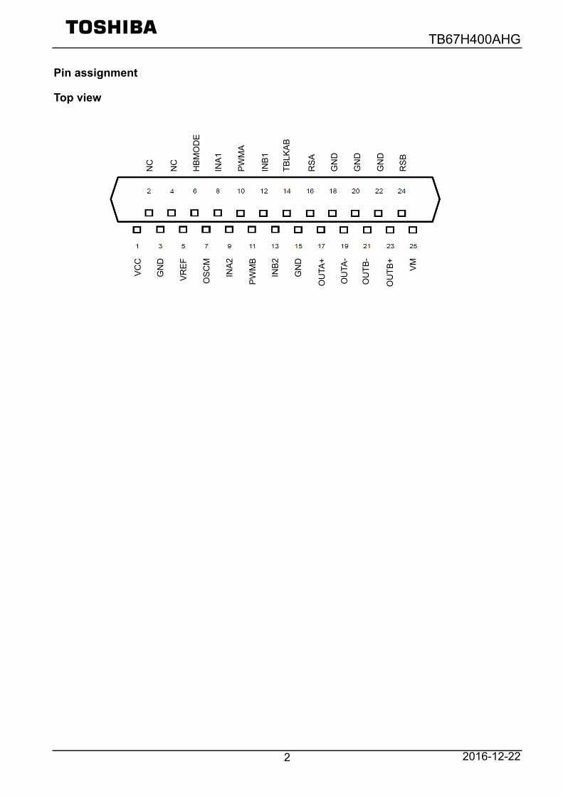
Function mode (Small Mode condition) Logic input function table (1) INA1, INA2 These pins set the drive mode for Motor A ch.
PWMA INA1 INA2 OUTA+ OUTA- Function
INPUT
L L L OFF (Hi-Z) OFF (Hi-Z)
STANDBY MODE (Note)
H STOP (OFF)
L L H
L L Short brake
H L H CCW (Counter clock-wise)
L H L
L L Short brake
H H L CW (Clock-wise)
L H H L L Short brake
H
(2) INB1, INB2 These pins set the drive mode for Motor B ch.
PWMB INB1 INB2 OUTB+ OUTB- Function
INPUT
L L L OFF (Hi-Z) OFF (Hi-Z)
STANDBY MODE (Note)
H STOP (OFF) L
L H L L Short brake
H L H CCW (Counter clock-wise)
L H L
L L Short brake H H L CW (Clock-wise) L
H H L L Short brake H
Note: The standby mode is only enabled when all 6 logic input pins (INA1, INA2, PWMA, INB1, INB2, and PWMB)
are set to Low level.

TB67H400AHG
2016-12-22
8
(3) TBLKAB This pin will set the noise rejection time.
TBLKAB TBLK noise rejection time
L Digital tBLK = fOSCM × 4 clk
H Digital tBLK = fOSCM × 6 clk
Please note that the timing charts or constants may be omitted or simplified for explanatory. * The Digital tBLK is used to avoid error judgment of varistor recovery current that occurs in charge drive mode when
H-bridges are used with DC motors. The Digital tBLK time can be controlled with TBLKAB pin. By setting Digital tBLK, direct PWM control and constant current control is possible, but the motor current will rise above the predefined current level (NF) while digital tBLK is active.
* Besides Digital tBLK, Analog tBLK (400 ns (typ.)) settled by an internal constant of IC is also attached. Digital tBLK timing for Brushed DC Motor The Digital tBLK is inserted at the beginning of each charge period of the constant current chopping, and also when either of INA1, INA2, INB1, or INB2 is switched. Please note that the timing charts or constants may be omitted or simplified for explanatory.
Digital tBLK
OSCM
0
1
2
3
TBLK count
IN1/IN2
Digital tBLK signal
(TBLKAB=L)
Synchronous delay
4
5
Digital tBLK signal
(TBLKAB=H) Digital tBLK
6
Digital tBLK
Iout
IN1 IN2

TB67H400AHG
2016-12-22
9
(4) HBMODE This pin sets the H-Bridge operation mode.
Pin name Function Input Setting
HBMODE H-Bridge
operation setting L Small mode
H Large mode Note: When using the Large mode, please make sure that the impedance between A channel and B channel is
balanced. Also, make sure that the output pins (OUTA+ and OUTA-, OUTB+ and OUTB-), RS pins (RSA and RSB) are connected to each other when using the Large mode.
Note: Please set the HBMODE to Low or High with the PCB pattern. (Do not change the logic input level during
operation.) Note: When the HBMODE pin is set to High level, the motor control will be controlled by the Ach inputs (INA1, INA2,
and PWMA). The Bch inputs (INB1, INB2, and PWMB) will be invalid. (When using the TB67H400AHG in the Large mode, setting the INB1, INB2, and PWMB to Low level is preferred.) TBLKAB pin is effective in both Small and Large modes (HBMODE=L/H).
H-Bridge connection example in each mode 2 Small DC motor operation setting example (HBMODE=L)
2 Small DC Motor operation
H-Bridge A
OUTA- OUTA+
RRS
VM
Load
H-Bridge B
Load
RRS
VM
OUTB- OUTB+
TB67H400AHG
2016-12-22
10
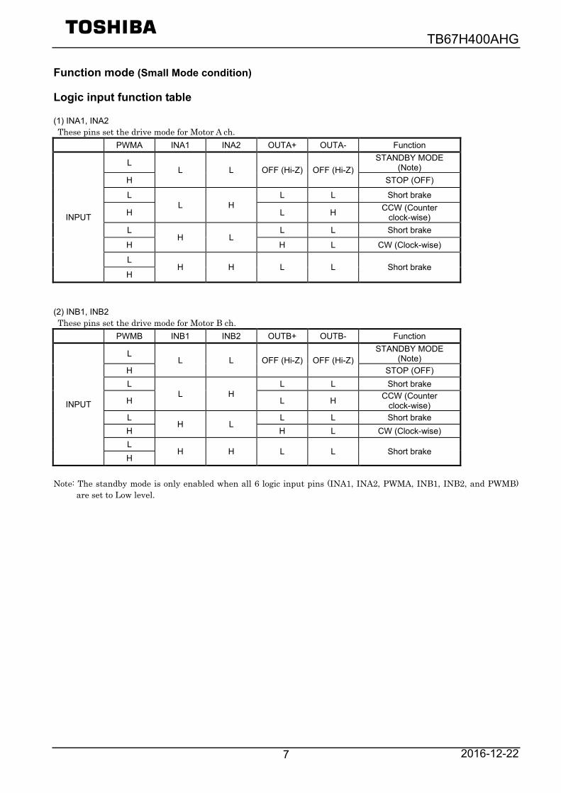
1 Large DC motor operation setting example (HBMODE=H) Please note that in the equivalent input circuit, functional blocks or constants may be omitted or simplified for explanatory purposes. DC Small mode: H-Bridge A and B will operate separately (for two brushed DC motor operation) DC Large mode: H-Bridge A and B will operate as a single H-Bridge. (for one brushed DC motor operation) * When the HBMODE is set to High level (Large mode), the pin function will be as follows.
Pin HBMODE=H (Large mode)
INA1 INL1
INA2 INL2
PWMA PWML
PWMB Don’t care (Motor will be
Controlled by INL1, INL2, and PWML pins) INB1
INB2
TBLKAB TBLKL
RSA RSL
RSB
OUTA+ OUTL+
OUTA-
OUTB+ OUTL-
OUTB-
Note: Please connect the “RSA and RSB”, “OUTA+ and OUTA-“, and “OUTB+ and OUTB-“when using the Large mode
operation.
1 Large DC Motor operation
H-Bridge A
OUTA- OUTA+
RRS
VM
H-Bridge B
Load
OUTB- OUTB+

TB67H400AHG
2016-12-22
11
Motor control (constant current control) Current waveform of Mixed Decay Mode, and a setting
In the case of constant current control, the rate of Mixed Decay Mode which determines the current ripple is fixed to 37.5%. Mixed Decay Mode current waveform Please note that the timing charts or constants may be omitted or simplified for explanatory.
1/fchop
Internal OSC waveform
MDT (Mixed Decay Timing): 37.5% fixed
fchop 1 cycle: 16clk
6clk / 16clk = 37.5% fchop
Charge Mode → NF detect → Slow Mode → Mixed Decay Timing → Fast Mode → Charge Mode
IOUT
Setting current value
MDT (Mixed Decay Timing):37.5% fixed
Setting current value
37.5% Mixed Decay Mode
Internal OSC waveform
IOUT
1/fchop
1/fchop
37.5% Mixed Decay Mode
NF detect
NF detect
NF detect
TB67H400AHG
2016-12-22
12
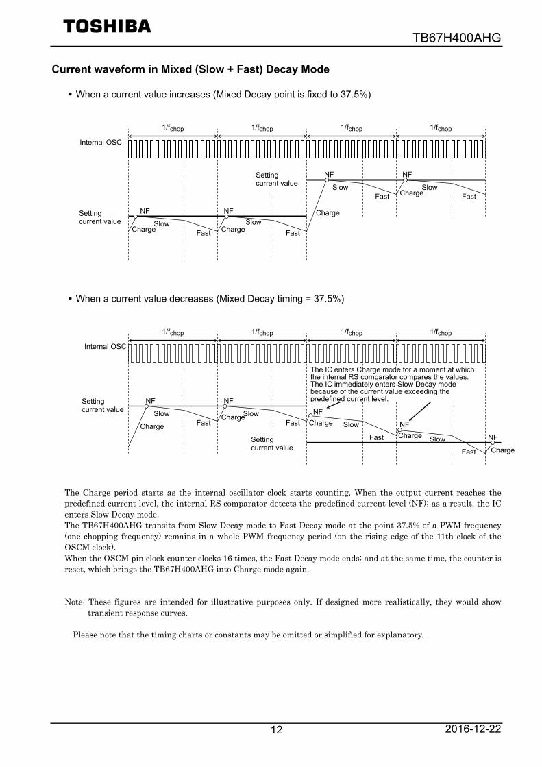
Current waveform in Mixed (Slow + Fast) Decay Mode When a current value increases (Mixed Decay point is fixed to 37.5%)
When a current value decreases (Mixed Decay timing = 37.5%)
The Charge period starts as the internal oscillator clock starts counting. When the output current reaches the predefined current level, the internal RS comparator detects the predefined current level (NF); as a result, the IC enters Slow Decay mode. The TB67H400AHG transits from Slow Decay mode to Fast Decay mode at the point 37.5% of a PWM frequency (one chopping frequency) remains in a whole PWM frequency period (on the rising edge of the 11th clock of the OSCM clock). When the OSCM pin clock counter clocks 16 times, the Fast Decay mode ends; and at the same time, the counter is reset, which brings the TB67H400AHG into Charge mode again.
Note: These figures are intended for illustrative purposes only. If designed more realistically, they would show transient response curves.
Please note that the timing charts or constants may be omitted or simplified for explanatory.
NF
NF
Internal OSC
Setting current value
Charge
1/fchop 1/fchop
1/fchop
1/fchop
NF
Setting current value
Charge Slow
Slow Charge Fast
Fast
NF NF
Slow Fast
Slow Charge Fast
The IC enters Charge mode for a moment at which the internal RS comparator compares the values. The IC immediately enters Slow Decay mode because of the current value exceeding the predefined current level.
Charge
Internal OSC
Setting current value
1/fchop 1/fchop
1/fchop
1/fchop
NF NF
NF NF
Charge Slow Slow
Charge Fast Fast
Charge
Slow Fast
Slow Charge Fast
Setting current value
TB67H400AHG
2016-12-22
13
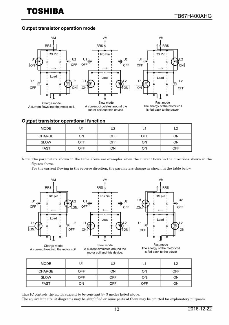
Output transistor operation mode Output transistor operational function
MODE U1 U2 L1 L2
CHARGE ON OFF OFF ON
SLOW OFF OFF ON ON
FAST OFF ON ON OFF
Note: The parameters shown in the table above are examples when the current flows in the directions shown in the
figures above. For the current flowing in the reverse direction, the parameters change as shown in the table below.
MODE U1 U2 L1 L2
CHARGE OFF ON ON OFF
SLOW OFF OFF ON ON
FAST ON OFF OFF ON
This IC controls the motor current to be constant by 3 modes listed above. The equivalent circuit diagrams may be simplified or some parts of them may be omitted for explanatory purposes.
Charge mode A current flows into the motor coil.
Slow mode A current circulates around the
motor coil and this device.
Fast mode The energy of the motor coil
is fed back to the power
Charge mode A current flows into the motor coil.
Slow mode A current circulates around the
motor coil and this device.
Fast mode The energy of the motor coil
is fed back to the power
U1
L1
U2
L2
OFF
OFF
U1
L1
U2
L2
OFF
ON ON
Load
U1
L1
U2
L2
Load
RS pin
RRS
VM
ON
ON
Load
ON
RS pin
RRS
VM
RS pin
RRS
VM
OFF
OFF ON OFF
U1
L1
U2
L2
OFF
OFF
U1
L1
U2
L2
OFF
ON ON
Load
U1
L1
U2
L2
Load
RS Pin
RRS
VM
ON
ON
Load
ON
RS Pin
RRS
VM
RS Pin
RRS
VM
OFF
OFF ON OFF
TB67H400AHG
2016-12-22
14
Calculation of the predefined output current For PWM constant current control, this IC uses a clock generated by the OSCM oscillator. The peak output current (Setting current value) can be set via the current-sensing resistor (RRS) and the reference voltage (Vref), as follows: Iout (max) = Vref (gain) ×
Vref (gain): the Vref decay rate is 1 / 5.0 (typ.) For example: In the case of a 100% setup When Vref is 3.0 V and RSS is 0.51 Ω, the motor constant current (Peak current) will be calculated as: Iout = 3.0 V / 5.0 / 0.51 Ω= 1.18 A Calculation of the OSCM oscillation frequency (chopper reference frequency) An approximation of the OSCM oscillation frequency (fOSCM) and chopper frequency (fchop) can be calculated by the following expressions.
fOSCM = 1/ [0.56 × COSC × (ROSC + 500)] * COSC, ROSC: External components for OSCM (When COSC is 270 pF and ROSC is 5.1 kΩ, fOSCM is about
1.12 MHz (typ.).) fchop = fOSCM / 16 * When fOSCM is 1.12 MHz, fchop is about 70 kHz (typ.).
If chopping frequency is raised, the ripple of current will become small and wave-like reproducibility will improve. However, the gate loss inside IC goes up and generation of heat becomes large. The standard frequency is about 70 kHz. A setup in the range of 50 to 100 kHz is recommended.
Vref (V)
RRS (Ω)

TB67H400AHG
2016-12-22
15
Absolute maximum ratings (Ta = 25°C)
Characteristics Symbol Rating Unit Remarks
Motor power supply VM 50 V ― Motor output voltage Vout 50 V ―
Motor output current Iout(S) 4.0 A
Small mode (Note1)
Iout(L) 8.0 A Large mode
(Note1) VCC voltage VCC 6.0 V ―
Digital input voltage VIN(H) 6.0 V ― VIN(L) -0.4 V ―
Vref input voltage Vref GND to 4.2 V ― Power dissipation PD 3.5 W (Note2)
Operating temperature Topr -20 to 85 °C ― Storage temperature Tstg -55 to 150 °C ― Junction temperature Tj 150 °C ―
Note1: While in use, please make sure to take the heat generation matter into consideration, and use below 70% of the
absolute maximum ratings (Iout(S) ≤ 2.8 A, Iout(L) ≤ 5.6 A) as a reference. Operating conditions (such as surrounding temperature or board conditions) may limit the operating current. (Depends on the heat conditions.)
Note2: The value in the state where it is not mounted on the board. Ta exceeding 25°C would require derating at 28.0 mW/°C.
Ta : Ambient temperature. Topr : Operating ambient temperature. Tj : Operating junction temperature. The maximum junction temperature is limited by the thermal shutdown
circuit (TSD). Use the maximum junction temperature (Tj) at 120°C or less. The maximum current cannot be used under certain thermal conditions.
Caution) Absolute maximum ratings The absolute maximum ratings of a semiconductor device are a set of ratings that must not be exceeded, even for a moment. Do not exceed any of these ratings. Exceeding the rating (s) may cause device breakdown, damage or deterioration, and may result in injury by explosion or combustion. The value of even one parameter of the absolute maximum ratings should not be exceeded under any circumstances. The TB67H400AHG does not have overvoltage detection circuit. Therefore, the device is damaged if a voltage exceeding its rated maximum is applied. All voltage ratings, including supply voltages, must always be followed. The other notes and considerations described later should also be referred to. Operating ranges (Ta=-20 to 85°C)
Characteristics Symbol Min Typ. Max Unit Remarks
VM power supply VM 10 24 47 V ―
Motor output current Iout(S) - 1.5 3.0 A Small mode Iout(L) - 3.0 6.0 A Large mode
Logic input voltage VIN(H) 2.0 ― 5.5 V Logic [High] level
VIN(L) GND ― 0.8 V Logic [Low] level
Logic input frequency fLOGIC ― ― 400 kHz IN1, IN2, PWM PWM signal frequency fchop(range) 40 70 150 kHz ―
Vref input voltage Vref GND 2.0 4.0 V ―
Note: The actual maximum current may be limited by the operating environment (operating conditions such operating duration, or by the surrounding temperature or board heat dissipation). Determine a realistic maximum current by calculating the heat generated under the operating environment.

TB67H400AHG
2016-12-22
16
Electrical characteristics 1 (Ta=25°C and VM=24 V, unless otherwise specified)
Characteristics Symbol Test conditions Min Typ. Max Unit
Logic input voltage High VIN(H) Logic input pins (Note) 2.0 ― 5.5 V Low VIN(L) Logic input pins (Note) 0 ― 0.8 V
Logic input hysteresis voltage VIN(HYS) Logic input pins (Note) 100 ― 300 mV
Logic input current High IIN(H) Logic input pins:3.3 V ― 33 ― µA Low IIN(L) Logic input pins:0 V ― ― 1 µA
Power consumption
IM1 Output: OPEN, Standby mode ― 2 3.5 mA
IM2 Output: OPEN, PWM=H,
IN1, IN2=Low ― 3.5 5.5 mA
IM3 Output: OPEN ― 5.5 7 mA
Output leakage current High IOH VRS=VM=50 V, Vout=0 V ― ― 1 µA Low IOL VRS=VM=Vout=50 V 1 ― ― µA
Output current channel differential ΔIout1 Bridge A, B differential -5 0 5 % Output current accuracy ΔIout2 Iout=1.5 A -5 0 5 %
RS pin current IRS VRS=VM=24 V 0 ― 10 µA
Drain-source ON-resistance (High side + low side) Ron(H+L)
Tj=25°C, Forward direction High side+Low side
Small mode ― 0.49 0.6 Ω
Note: VIN(H) is defined as the VIN voltage that causes the outputs (OUTA+, OUTA-, OUTB+ and OUTB-) to change
when a pin under test is gradually raised from 0 V. VIN(L) is defined as the VIN voltage that causes the outputs (OUTA+, OUTA-, OUTB+ and OUTB-) to change when the pin is then gradually lowered. The difference between VIN(H) and VIN(L) is defined as the VIN(HYS).
Note: The internal circuits are designed to avoid miss-function or leakage current; when the logic signal is applied
while the VM voltage is not supplied. But for fail-safe, please control the power supply and logic signal timing correctly.
TB67H400AHG
2016-12-22
17
Electrical characteristics 2 (Ta=25°C and VM=24 V, unless otherwise specified)
Characteristics Symbol Test conditions Min Typ. Max Unit
Vref input current Iref Vref=2.0 V ― 0 1 μA
Internal regulator voltage VCC ICC=5.0 mA 4.75 5.0 5.25 V
Internal regulator current ICC VCC=5.0 V ― 2.5 5 mA
Vref gain rate Vref(gain) Vref=2.0 V 1/5.2 1/5.0 1/4.8 ―
TSD threshold (Note1) TjTSD ― 145 160 175 °C
VM power on reset voltage VMR ― 7.0 8.0 9.0 V
Over current threshold (Note2) ISD ― 4.1 4.9 5.7 A Note1: Thermal shutdown (TSD) circuit
When the junction temperature of the device reaches the TSD threshold, the TSD circuit is triggered; the internal reset circuit then turns off the output transistors. In order to avoid malfunction by switching etc., detection mask time is prepared inside IC. Once the TSD circuit is triggered, the device will be set to standby mode, and can be cleared by reasserting the VM power source, or setting to standby mode (INA1, INA2, INB1, INB2, PWMA, and PWMB=All Low). The TSD circuit is a backup function to detect a thermal error, therefore is not recommended to be used aggressively.
Note2: Over-current shutdown (ISD) circuit
When the output current reaches the threshold, the ISD circuit is triggered; the internal reset circuit then turns off the output transistors. In order to avoid malfunction by switching etc., detection mask time is prepared inside IC. Once the ISD circuit is triggered, the device will be set to standby mode, and can be cleared by reasserting the VM power source, or setting to standby mode (INA1, INA2, INB1, INB2, PWMA, and PWMB=All Low).
Back-EMF While a motor is rotating, there is a timing at which power is fed back to the power supply. At that timing, the motor current recirculates back to the power supply due to the effect of the motor back-EMF. If the power supply does not have enough sink capability, the power supply and output pins of the device might rise above the rated voltages. The magnitude of the motor back-EMF varies with usage conditions and motor characteristics. It must be fully verified that there is no risk that the TB67H400AHG or other components will be damaged or fail due to the motor back-EMF. Cautions on Overcurrent Shutdown (ISD) and Thermal Shutdown (TSD) The ISD and TSD circuits are only intended to provide temporary protection against irregular conditions such as an output short-circuit; they do not necessarily guarantee the complete IC safety. If the device is used beyond the specified operating ranges, these circuits may not operate properly: then the device may be damaged due to an output short-circuit. The ISD circuit is only intended to provide a temporary protection against an output short-circuit. If such a condition persists for a long time, the device may be damaged due to overstress. Overcurrent conditions must be removed immediately by external hardware. IC Mounting Do not insert devices incorrectly or in the wrong orientation. Otherwise, it may cause breakdown, damage and/or deterioration of the device.
TB67H400AHG
2016-12-22
18
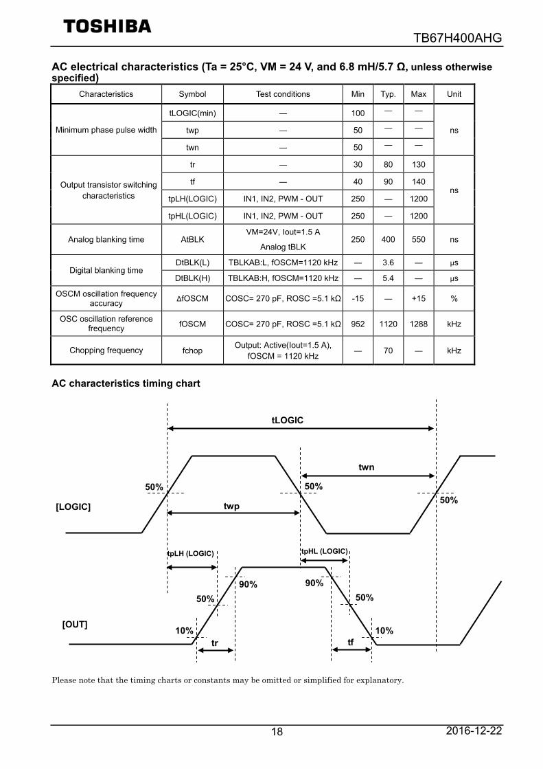
AC electrical characteristics (Ta = 25°C, VM = 24 V, and 6.8 mH/5.7 Ω, unless otherwise specified)
Characteristics Symbol Test conditions Min Typ. Max Unit
Minimum phase pulse width
tLOGIC(min) ― 100 ― ―
ns twp ― 50 ― ―
twn ― 50 ― ―
Output transistor switching characteristics
tr ― 30 80 130
ns tf ― 40 90 140
tpLH(LOGIC) IN1, IN2, PWM - OUT 250 ― 1200
tpHL(LOGIC) IN1, IN2, PWM - OUT 250 ― 1200
Analog blanking time AtBLK VM=24V, Iout=1.5 A
Analog tBLK 250 400 550 ns
Digital blanking time DtBLK(L) TBLKAB:L, fOSCM=1120 kHz ― 3.6 ― μs
DtBLK(H) TBLKAB:H, fOSCM=1120 kHz ― 5.4 ― μs
OSCM oscillation frequency accuracy ΔfOSCM COSC= 270 pF, ROSC =5.1 kΩ -15 ― +15 %
OSC oscillation reference frequency fOSCM COSC= 270 pF, ROSC =5.1 kΩ 952 1120 1288 kHz
Chopping frequency fchop Output: Active(Iout=1.5 A),
fOSCM = 1120 kHz ― 70 ― kHz
AC characteristics timing chart Please note that the timing charts or constants may be omitted or simplified for explanatory.
twp
twn
tpLH (LOGIC) tpHL (LOGIC)
10%
90%
tr
90%
10% tf
[LOGIC]
[OUT]
50% 50%
50% 50% 50%
tLOGIC

TB67H400AHG
2016-12-22
19
(Reference) Relation between the power dissipation and the ambient temperature
This value is dependent on a substrate pattern and mounting conditions. Moreover, when ambient temperature is high, permissible power consumption becomes small.
Device alone conditions
TB67H400AHG
2016-12-22
20
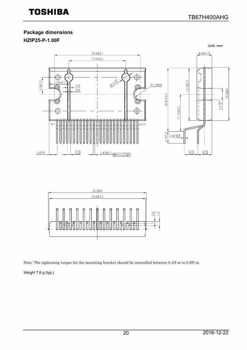
Package dimensions HZIP25-P-1.00F
Unit: mm
Note: The tightening torque for the mounting bracket should be controlled between 0.4N∙m to 0.6N∙m. Weight 7.6 g (typ.)
TB67H400AHG
2016-12-22
21
Notes on Contents Block Diagrams
Some of the functional blocks, circuits, or constants in the block diagram may be omitted or simplified for explanatory purposes.
Equivalent Circuits The equivalent circuit diagrams may be simplified or some parts of them may be omitted for explanatory purposes.
Timing Charts Timing charts may be simplified for explanatory purposes.
Application Circuits The application circuits shown in this document are provided for reference purposes only. Thorough evaluation is required at the mass production design stage. Toshiba does not grant any license to any industrial property rights by providing these examples of application circuits.
Test Circuits Components in the test circuits are used only to obtain and confirm the device characteristics. These components and circuits are not guaranteed to prevent malfunction or failure from occurring in the application equipment. IC Usage Considerations
Notes on handling of ICs The absolute maximum ratings of a semiconductor device are a set of ratings that must not be exceeded, even for a moment. Do not exceed any of these ratings. Exceeding the rating(s) may cause device breakdown, damage or deterioration, and may result in injury by explosion or combustion. Use an appropriate power supply fuse to ensure that a large current does not continuously flow in the case of over-current and/or IC failure. The IC will fully break down when used under conditions that exceed its absolute maximum ratings, when the wiring is routed improperly or when an abnormal pulse noise occurs from the wiring or load, causing a large current to continuously flow and the breakdown can lead to smoke or ignition. To minimize the effects of the flow of a large current in the case of breakdown, appropriate settings, such as fuse capacity, fusing time and insertion circuit location, are required. If your design includes an inductive load such as a motor coil, incorporate a protection circuit into the design to prevent device malfunction or breakdown caused by the current resulting from the inrush current at power ON or the negative current resulting from the back electromotive force at power OFF. IC breakdown may cause injury, smoke or ignition. Use a stable power supply with ICs with built-in protection functions. If the power supply is unstable, the protection function may not operate, causing IC breakdown. IC breakdown may cause injury, smoke or ignition.
Do not insert devices in the wrong orientation or incorrectly. Make sure that the positive and negative terminals of power supplies are connected properly. Otherwise, the current or power consumption may exceed the absolute maximum rating, and exceeding the rating(s) may cause device breakdown, damage or deterioration, and may result in injury by explosion or combustion. In addition, do not use any device that has been inserted incorrectly. Please take extra care when selecting external components (such as power amps and regulators) or external devices (for instance, speakers). When large amounts of leak current occurs from capacitors, the DC output level may increase. If the output is connected to devices such as speakers with low resist voltage, overcurrent or IC failure may cause smoke or ignition. (The over-current may cause smoke or ignition from the IC itself.) In particular, please pay attention when using a Bridge Tied Load (BTL) connection-type IC that inputs output DC voltage to a speaker directly.

TB67H400AHG
2016-12-22
22
Points to remember on handling of ICs Over current detection circuit Over current detection circuits (referred to as current limiter circuits) do not necessarily protect ICs under all circumstances. If the Over current detection circuits operate against the over current, clear the over current status immediately. Depending on the method of use and usage conditions, such as exceeding absolute maximum ratings can cause the over current protection circuit to not operate properly or IC breakdown before operation. In addition, depending on the method of use and usage conditions, if over current continues to flow for a long time after operation, the IC may generate heat resulting in breakdown. Thermal Shutdown Circuit Thermal shutdown circuits do not necessarily protect ICs under all circumstances. If the thermal shutdown circuits operate against the over temperature, clear the heat generation status immediately. Depending on the method of use and usage conditions, such as exceeding absolute maximum ratings can cause the thermal shutdown circuit to not operate properly or IC breakdown before operation. Heat Radiation Design In using an IC with large current flow such as power amp, regulator or driver, please design the device so that heat is appropriately radiated, not to exceed the specified junction temperature (Tj) at any time and condition. These ICs generate heat even during normal use. An inadequate IC heat radiation design can lead to decrease in IC life, deterioration of IC characteristics or IC breakdown. In addition, please design the device taking into considerate the effect of IC heat radiation with peripheral components. Back-EMF When a motor rotates in the reverse direction, stops or slows down abruptly, a current flow back to the motor’s power supply due to the effect of back-EMF. If the current sink capability of the power supply is small, the device’s motor power supply and output pins might be exposed to conditions beyond maximum ratings. To avoid this problem, take the effect of back-EMF into consideration in system design.
TB67H400AHG
2016-12-22
23
RESTRICTIONS ON PRODUCT USE
• Toshiba Corporation, and its subsidiaries and affiliates (collectively "TOSHIBA"), reserve the right to make changes to the information in this document, and related hardware, software and systems (collectively "Product") without notice.
• This document and any information herein may not be reproduced without prior written permission from TOSHIBA. Even with TOSHIBA's written permission, reproduction is permissible only if reproduction is without alteration/omission.
• Though TOSHIBA works continually to improve Product's quality and reliability, Product can malfunction or fail. Customers are responsible for complying with safety standards and for providing adequate designs and safeguards for their hardware, software and systems which minimize risk and avoid situations in which a malfunction or failure of Product could cause loss of human life, bodily injury or damage to property, including data loss or corruption. Before customers use the Product, create designs including the Product, or incorporate the Product into their own applications, customers must also refer to and comply with (a) the latest versions of all relevant TOSHIBA information, including without limitation, this document, the specifications, the data sheets and application notes for Product and the precautions and conditions set forth in the "TOSHIBA Semiconductor Reliability Handbook" and (b) the instructions for the application with which the Product will be used with or for. Customers are solely responsible for all aspects of their own product design or applications, including but not limited to (a) determining the appropriateness of the use of this Product in such design or applications; (b) evaluating and determining the applicability of any information contained in this document, or in charts, diagrams, programs, algorithms, sample application circuits, or any other referenced documents; and (c) validating all operating parameters for such designs and applications. TOSHIBA ASSUMES NO LIABILITY FOR CUSTOMERS' PRODUCT DESIGN OR APPLICATIONS.
• PRODUCT IS NEITHER INTENDED NOR WARRANTED FOR USE IN EQUIPMENTS OR SYSTEMS THAT REQUIRE EXTRAORDINARILY HIGH LEVELS OF QUALITY AND/OR RELIABILITY, AND/OR A MALFUNCTION OR FAILURE OF WHICH MAY CAUSE LOSS OF HUMAN LIFE, BODILY INJURY, SERIOUS PROPERTY DAMAGE AND/OR SERIOUS PUBLIC IMPACT ("UNINTENDED USE"). Except for specific applications as expressly stated in this document, Unintended Use includes, without limitation, equipment used in nuclear facilities, equipment used in the aerospace industry, medical equipment, equipment used for automobiles, trains, ships and other transportation, traffic signaling equipment, equipment used to control combustions or explosions, safety devices, elevators and escalators, devices related to electric power, and equipment used in finance-related fields. IF YOU USE PRODUCT FOR UNINTENDED USE, TOSHIBA ASSUMES NO LIABILITY FOR PRODUCT. For details, please contact your TOSHIBA sales representative.
• Do not disassemble, analyze, reverse-engineer, alter, modify, translate or copy Product, whether in whole or in part.
• Product shall not be used for or incorporated into any products or systems whose manufacture, use, or sale is prohibited under any applicable laws or regulations.
• The information contained herein is presented only as guidance for Product use. No responsibility is assumed by TOSHIBA for any infringement of patents or any other intellectual property rights of third parties that may result from the use of Product. No license to any intellectual property right is granted by this document, whether express or implied, by estoppel or otherwise.
• ABSENT A WRITTEN SIGNED AGREEMENT, EXCEPT AS PROVIDED IN THE RELEVANT TERMS AND CONDITIONS OF SALE FOR PRODUCT, AND TO THE MAXIMUM EXTENT ALLOWABLE BY LAW, TOSHIBA (1) ASSUMES NO LIABILITY WHATSOEVER, INCLUDING WITHOUT LIMITATION, INDIRECT, CONSEQUENTIAL, SPECIAL, OR INCIDENTAL DAMAGES OR LOSS, INCLUDING WITHOUT LIMITATION, LOSS OF PROFITS, LOSS OF OPPORTUNITIES, BUSINESS INTERRUPTION AND LOSS OF DATA, AND (2) DISCLAIMS ANY AND ALL EXPRESS OR IMPLIED WARRANTIES AND CONDITIONS RELATED TO SALE, USE OF PRODUCT, OR INFORMATION, INCLUDING WARRANTIES OR CONDITIONS OF MERCHANTABILITY, FITNESS FOR A PARTICULAR PURPOSE, ACCURACY OF INFORMATION, OR NONINFRINGEMENT.
• Do not use or otherwise make available Product or related software or technology for any military purposes, including without limitation, for the design, development, use, stockpiling or manufacturing of nuclear, chemical, or biological weapons or missile technology products (mass destruction weapons). Product and related software and technology may be controlled under the applicable export laws and regulations including, without limitation, the Japanese Foreign Exchange and Foreign Trade Law and the U.S. Export Administration Regulations. Export and re-export of Product or related software or technology are strictly prohibited except in compliance with all applicable export laws and regulations.
• Please contact your TOSHIBA sales representative for details as to environmental matters such as the RoHS compatibility of Product. Please use Product in compliance with all applicable laws and regulations that regulate the inclusion or use of controlled substances, including without limitation, the EU RoHS Directive. TOSHIBA ASSUMES NO LIABILITY FOR DAMAGES OR LOSSES OCCURRING AS A RESULT OF NONCOMPLIANCE WITH APPLICABLE LAWS AND REGULATIONS.