Embed Size (px)
Citation preview

������� �����
Ver3.7 00/01/28 1
TENTATIVE TOSHIBA Bi-CMOS INTEGRATED CIRCUIT, SILICON MONOLITHIC
TB1254NPAL / NTSC / SECAM 1CHIP (IF+VCD PROCESSOR) IC
The TB1254N is a TV signal processor IC, which containsPIF, SIF, Video, Chroma and deflection signal processorsfor worldwide Multi-color systems. Also, it has AV switchfor TV/EXT inputs.
The line-up and flexibility of this TB1251 series contributesto reduce development costs and components in a TVsets.
FEATURES IF STAGE
� Multi-system IF� SIF 4.5 ~ 6.5 MHz� One External BPF for Multi-SIF carrier� Inter carrier inputs� VCO tank coil alignment free� for L system,
Positive demodulationV low Ch
VIDEO STAGE� Built-in Y delay line (8 adjustable steps)� Built in C trap filter (Switchable)
CHROMA STAGE� Multi-color Demoduration� Automatic Chroma Identification� 1 Xtal for Multi-color Systems (3.58MHz/4.43MHz/M-PAL/N-PAL)� Built-in1H Delay line� Cb/Cr input ports� Built-in BPF / TOF� Fsc Output� Two NTSC demodulation phase
SDIP56-P-600
TEXT STAGE� Built-in AKB
AKB on/offAKB Color temperature control
� Analog RGB interfaces� ABL / ACL
DEFLECTION STAGE� Built-in H-VCO� ramp distortion correction� Stand Along Sync in port� Sand Castle Pulse Output
(HD+VD+Gate Pulse)
AV SWITCH� Visual TV / EXT inputs� Audio TV / EXT inputs
� TOSHIBA is continually working to improve the quality and the reliability of its products. Nevertheless,semiconductor devices in general can malfunction or jail due to their inherent electrical sensitivity andvulnerability to physical stress. It is the responsibility of the buyer, when utilizing TOSHIBA products, toobserve standards of safety, and to avoid situations in which a malfunction or failure of a TOSHIBA product couldcause loss of human life, bodily injury or damage to property. In developing your designs, please ensure thatTOSHIBA products are used within specified operating range as set forth in the most recent products specifications.Also, please keep in mind the precautions and conditions set forth in the TOSHIBA Semiconductor ReliabilityHandbook.
� The products described in this document are subject to foreign exchange and foreign trade control laws.� The information contained herein is presented only as a guide for the applications of our products. No
responsibility is assumed by TOSHIBA CORPORATION for any infringements of intellectual property or other rights ofth thi d ti hi h lt f it N li i t d b i li ti th i d
Weight: 5.55g (typ)

������� �����
Ver3.7 00/01/28 2
5650
5152
5354
5549
4344
4546
4748
4236
3738
3940
4135
2930
3132
3334
17
65
43
28
1413
1211
109
1521
2019
1817
1622
2827
2625
2423
SDA
SCL
Sync in
I2C
Bus
IF
Cut
off/D
rive
<R.G
.B.C
UTT
OFF
><R
.G.B
.DR
IVE
><A
KB
SW
><A
KB
W/B
con
trole
>
Mat
rix /
SW
RG
B In
terfa
ceB
right
<R
GB
BR
T>U
ni-C
olor
<RG
B C
ON
T>
Mod
e S
W
EW
PR
OC
.<H
.SIZ
E>
<EW
PA
RA
.><T
RA
PE
ZIU
M>
<EW
CO
NE
R>
TB
1254
N B
LOC
K D
IAG
RA
M
EH
T H
/V<E
HT.
H>
<EH
T.V
>
Y IN
V P
RO
C.
<V.S
IZE
><V
.LIN
EA
R.>
<V-S
CO
RR
.><V
.SH
IFT>
FM D
EM
OD
.
Gai
n S
w
AU
DIO
ATT
<ATT
>
Chr
oma
DE
MO
D.
PA
L/N
TSC
/SE
CA
M1H
del
ay li
ne1
X'ta
l<T
INT>
<col
or s
yste
m>
<F ID
><K
iller
Sen
ce>
PIF
Pro
c.
L-S
EC
AM
DE
F P
roc.
H,V
syn
chro
niza
tion
<Loc
k de
t.><S
ync
det>
<AFC
1 G
ain>
Chr
oma
Bas
eban
d P
roc.
<Col
or>
<Uni
colo
r>
Cla
mp
BB
TIN
T
6dB
IF INSA
W
IF GND
Ripple F
IF AGC
+
APC Filter
+
4.43MHz X'tal
CW OUT
Ys/Ym
EXT.R IN
EXT.G IN
EXT.B IN
RGB Vcc(9V)
+
R OUT
G OUT
B OUT
IK IN
V RAMP
V NFB
V OUT
EXT AUDIO IN
DC NF+
EXT IN
C in
BLACK Det+
Cb in
DC Restor
ABCL IN
YC Vcc(5V)+
Dig GND
YC GND
H OUT
H Vcc(9V)
H.AFC
FBP IN/SCP OUT
DE-EMP.
Dig.VDD
+
+
TV in
IF DET OUT
Hcorr IN/SIF IN
PIF
tank
+
6.5M
Hz
‚a‚o
‚eTR
AP
Y P
roc.
Cla
mp
C-T
RA
P<c
-trap
> B
lack
Stre
tch
<B.S
.> D
C re
stor
e<D
C re
st>
Y-ƒ
Á<ƒ
Á>
Y-D
.L.
<DL>
A.C
.<P
.SH
AR
P>
Sub
-Con
t<S
.CO
NT>
Uni
-Col
or<C
ON
T> B
right
<BR
T> W
PS
Hal
f T.
<H.T
><A
BL
STA
RT
P>
<AB
L G
AIN
>
IF Vcc(5V)+
LOOP Filter+
SIF OUT
AUDIO OUT
AFT OUT
MONITOR OUT
Cr in
ref R
SIF
Pro
cess
or6.
5MH
z
Uni
-SIF
bee
t up
RF AGC
+
N.C.
BIA
S
������� �����
Ver3.7 00/01/28 3
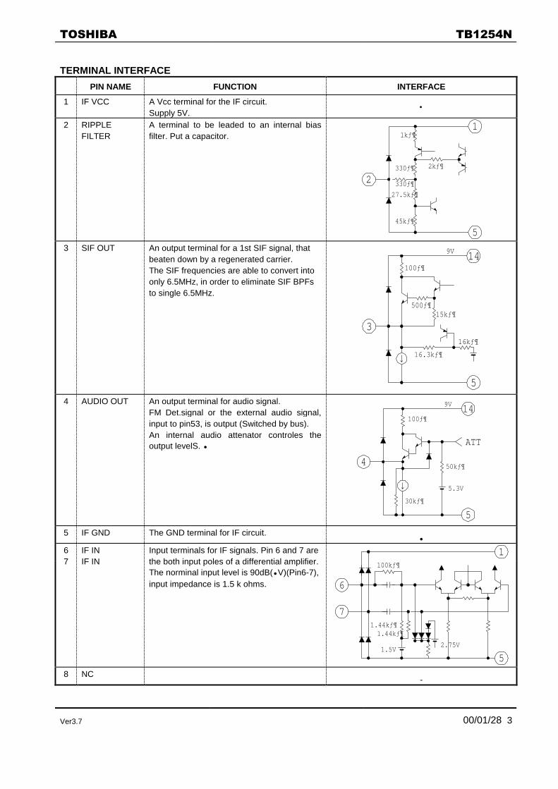
TERMINAL INTERFACE
PIN NAME FUNCTION INTERFACE
1 IF VCC A Vcc terminal for the IF circuit.Supply 5V.
•
2 RIPPLEFILTER
A terminal to be leaded to an internal biasfilter. Put a capacitor.
2
5
1
330Ħ
330Ħ
27.5kĦ
45kĦ
2kĦ
1kĦ
3 SIF OUT An output terminal for a 1st SIF signal, thatbeaten down by a regenerated carrier.The SIF frequencies are able to convert intoonly 6.5MHz, in order to eliminate SIF BPFsto single 6.5MHz.
3
5
14100Ħ
500Ħ15kĦ
9V
16.3kĦ
16kĦ
4 AUDIO OUT An output terminal for audio signal.FM Det.signal or the external audio signal,input to pin53, is output (Switched by bus).An internal audio attenator controles theoutput levelS. •
4
5
14
50kĦ
5.3V
ATT
9V
30kĦ
100Ħ
5 IF GND The GND terminal for IF circuit.•
67
IF INIF IN
Input terminals for IF signals. Pin 6 and 7 arethe both input poles of a differential amplifier.The norminal input level is 90dB(• V)(Pin6-7),input impedance is 1.5 k ohms. 6
5
1
7
100kĦ
1.44kĦ1.44kĦ
1.5V2.75V
8 NC-

������� �����
Ver3.7 00/01/28 4
PIN NAME FUNCTION INTERFACE
9 RF AGC An output terminal for RF AGC.
A pull up resister is required because of itsopen collector output, and also connect de-coupling capacitor to reduce noises,. 9
5
149V
300Ħ
30kĦ
30kĦ
to SELF ADJ
10 IF AGC A terminal to be connected to an IF AGCfilter. Connect 2.2• F of capacitor to Vcc
10
5
1
2kĦ
11 APC FILTER A terminal to be connected with an APC filterfor chroma demodulation.This terminal voltage controls the frequencyof VCXO.
11
19
42
220Ħ
110kĦ
3.2V
12 X’TAL(4.43MHZ)
A terminal to be connected with a4.433619MHz X’tal oscillator. The oscillatedsignal lead to chroma demodulation, H outfrequency tuning, AFT and so on.
12
19
42
500ƒ ¶2.5kƒ 
13 CW OUT An output terminal for the continuous chromasub-carrier frequency wave, which amplitudeis 0.7Vp-p (typ).Also the dc level shows killer status, the levelis 1.5V for B/W and 3.5V for Color.
13
19
42
200Ħ
1kĦ

������� �����
Ver3.7 00/01/28 5
PIN NAME FUNCTION INTERFACE
14 RGB VCC (9V) A Vcc terminal for RGB block, PIF det. Outputand sound output circuit.Supply 9V.
•
15 YS/YM SW• Spot killer
A terminal for switching of EXT RGB Modeand fast Half tone.
15
14
42
3.3V250Ħ
0.7V
161718
EXT. R INEXT. G INEXT. B IN
Input terminals for EXT RGB signals. Thesignals are clamped by capacitors, thereforethe input impedance should be low, 100ohms or less is recommended.For this input, brightness and RGB contrastare available, also ABL/ACL eliminate theoutput leval. This ABL/ACL is able to off. OFF: for small area like OSD ON: for large area like TELETEXT(input level 0.7Vp-p/100IRE)
16
19
42
250Ħ
250Ħ
2.3V
17
18
250Ħ
250Ħ
100uA
19 Y/C GND The GND terminal for Y/C circuit.•
202122
R OUTG OUTB OUT
Terminals for R/G/B signal output.Connect resistances to GND, if through rateis not enough. Because of source currentlimitation, the resistances should be 2.0k• ormore.
20
19
14
100Ħ
21
22
23 IK IN An input terminal to sense AKB cathodecurrent.Connect this terminals to GND if not usingthe AKB system.
23
19
42
2.5k
Ħ
2.5k
Ħ
5kĦ
2.5k
Ħ
25kƒ
50kƒ
12.5
kĦ
1kĦ
VF
VK
1kĦ
softstart
limitterover circuit
������� �����
Ver3.7 00/01/28 6
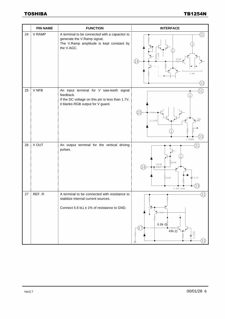
PIN NAME FUNCTION INTERFACE
24 V RAMP A terminal to be connected with a capacitor togenerate the V.Ramp signal.The V.Ramp amplitude is kept constant bythe V.AGC.
24
33
31
2.7k
Ħ
V AGC
200Ħ
25 V NFB An input terminal for V saw-teeth signalfeedback.If the DC voltage on this pin is less than 1.7V,it blanks RGB output for V guard.
12.5kĦ
25
33
31
2V
V GUARD
26 V OUT An output terminal for the vertical drivingpulses.
26
33
31
200Ħ30kĦ
1kĦ
V OUT read
0.5V
27 REF. R A terminal to be connected with resistance tostabilize internal current sources.
Connect 5.6 k� � 1% of resistance to GND.
27
33
1.12
V31
6.8k �
49k �

������� �����
Ver3.7 00/01/28 7
PIN NAME FUNCTION INTERFACE
28 ABCL IN An input terminal for ABL/ACL control.Control voltage range is 5.5• 6.0V.The ratio of ABL against ACL can be set bybus control.
29 H AFC FILTER A terminal to be connected with H. AFC Filter.The DC voltage of this pin controls the HVCO frequency.
29
33
31
100kĦ
50Ħ
237Ħ
75kƒ
30 FBP IN/ SCPOUT
An input terminal for FBP.The V and GP Pulses are overlaid as SCP.
protectGP
VD H AFC H BLK
30
33
313VF
VD
1.4V
3.5V
GP
31 H VCC (9V) A Vcc terminal for DEF circuit, HOUT,IICBUS POR etc.Supply 9V.
•
32 H OUT An output terminal for horizontal drivingpulses.
32
33
31
2VF6kĦ
50Ħ
33 DIG GND A GND terminal for digital block.•

������� �����
Ver3.7 00/01/28 8
PIN NAME FUNCTION INTERFACE
34 SCL An input terminal for IICBUS clock.
345kĦ
3.25V
31
33
35 SDA An input/output terminal for IICBUS data.
355kĦ
3.25V
31
33
36 BLACK DET A terminal to be connected with Black det.filter for black stretch.This terminal voltage controls Blackstretching gain.The IIC Bus controls on/off and start point ofBlack stretch.
36
2.5V
19
42
4kĦ
37 DIG. VDD A Vdd terminal for of digital block.Supply HVcc voltage through 270 ohms ofresistance.The voltage of this terminal is clipped inabout 3.3V by the internal regulator.
2.6V
30Ħ
30Ħ 750Ħ
37VDD
31H VCC
30Ħ

������� �����
Ver3.7 00/01/28 9
PIN NAME FUNCTION INTERFACE
38 SYNC IN An input terminal for Sync signal.The input sync chip is clamped bycharging/discharging the coupling capacitorsso as to align the Sync slice level, thereforeinput through low impedance buffer.(input level 1Vp-p/140IRE) 38
33
31
1kĦ6kĦ
24kĦ
832Ħ
3VF
39 Y IN An input terminal for Y signal.The pedestal level is clamped by means ofcharging/discharging the coupling capacitor,therefore input through low impedance buffer.(1Vp-p/140IRE input level) 39
1kĦ
1kĦ
1kĦ
<Amp> <Clamp> <read Bus>
42
19
40 DC RESTOR A terminal to be connected with a capacitor todetect the average picture level for DCrestoration.The ratio of the DC restoration is set by bus.Leave this terminal open if the DC restorationis not required. 40
19
42
10k
50k
41 MON OUT An output terminal of AV SW monitor.The input signal for pin # 46/48 is outputthrough 6dB amplifier .(output level 2Vp-p/140IRE)
41
19
14
8kĦ
8kĦ
2V
42 Y/C VCC An Vcc terminal for Y/C circuit.Supply 5V.
•

������� �����
Ver3.7 00/01/28 10
PIN NAME FUNCTION INTERFACE
43 C-IN An input terminal for chroma signal.(standard burst amplitude level 286mVp-p•
The low/High impedance status of this pincan be read by bus to detect if S port isconnected or not.
43
19
42
75kĦ
2.25V
1kĦ
4445
Cr INCb IN
Input terminals for Cb/Cr signals.This terminal is clamped by charging /discharging the coupling capacitors, thereforeinput with low impedance, 100• or less arerecommended.B.B.TINT• -/+12deg• Sub color control areavailable for Cb/Cr input signals.
44
19
42
clamp
2.5V
45
46 EXT IN An input terminal for external video signal.(input level 1Vp-p / 140 IRE)
46
19
14
2V
1kĦ
200ƒ
1kĦ
47 LOOP FILTER A terminal to be connected with loop filter forPIF PLL.The terminal voltage is controlled PIF VCOfrequency.
47
5
1
500Ħ
5V
1kĦ
1kĦ
15kĦ

������� �����
Ver3.7 00/01/28 11
PIN NAME FUNCTION INTERFACE
48 TV IN An input terminal for TV video signal.(input level 1Vp-p / 140 IRE)
48
19
14
2V
1kĦ
200ƒ
1kĦ
49 De-Emphasis• Mon-OUT
A terminal to De-Emphasis Audio signal, andpick up detected Audio signal. Connectcapacitor (0.01• F to GND.The time constant 50/75us is set by theIICBUS control “SIF Freq”.Remove the capacitor in case of use US/JPNsound multiplex system.
49
5
14
15kĦ 7.5kĦ 500Ħ
5051
PIF TANK Terminals to connect a PIF tank coil.The tank coil should be pre-set up within +/-2% for the automatic tuning. Manual tuning isalso available..The resonance capacitance of the tankshould be 18pF.
50
5
1
51
52 DC NF A terminal for connect the capacitor for DCNF.
52
5
14
2kĦ 10kĦ
������� �����
Ver3.7 00/01/28 12
PIN NAME FUNCTION INTERFACE
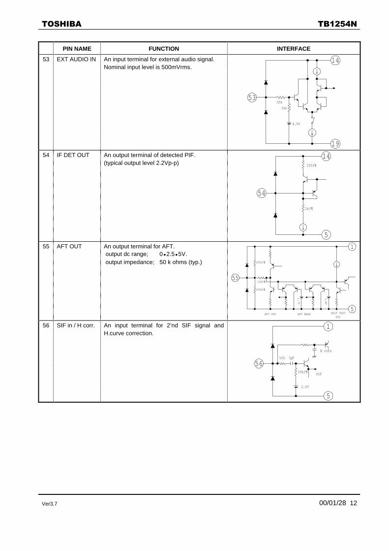
53 EXT AUDIO IN An input terminal for external audio signal.Nominal input level is 500mVrms.
53
19
14
4.5V
35k
35k
54 IF DET OUT An output terminal of detected PIF.(typical output level 2.2Vp-p)
54
200Ħ
1kĦ
5
14
55 AFT OUT An output terminal for AFT. output dc range; 0• 2.5• 5V. output impedance; 50 k ohms (typ.)
55
5
1
100kĦ
100Ħ
100kĦ
3.4V
1.7V
AFT OUT AFT READ SELF TESTOUT
56 SIF in / H corr. An input terminal for 2’nd SIF signal andH.curve correction.
56
1
5
20kĦ
7pF
2.5V
500
SIF
H corr

������� �����
Ver3.7 00/01/28 13
BUS CONTROL MAP for TB1254N
Write ModeSlave Address: 88 HEX
SubAddr.
D7MSB
D6 D5 D4 D3 D2 D1 D0LSB
PRESET
00 WPS Uni-Color 0000 000001 B.B. Brightness ( TV / Text ) 0100 000002 C-Trap Color 0100 000003 N Phase Sharpness 0010 000004 Y MUTE RGB Mt RGB Contrast 0110 000005 Y D.L. Sub Color 0011 000006 Video SW Au SW B.B.Tint 0001 000007 N-Comb TINT 0100 000008 SECAM R-Y Black Adjust SECAM B-Y Black Adjust 1000 100009 S- GP Phase
/ S- inhibitS-ID Sens Bell fo S-Black
MonitorL-SECAM
ModeL-S AGCSpeed-up
S-IDMode
0000 0000
0A PIF Freq SIF Freq. Color System 0000 00000B 6.5MHz
SIF FixAudio Att
0000 0000
0C BPF/TOF P/N-ID Sens
F ID Coringoff
SIF5.74MHz
PIF VCOAdj. Stop
PIF VCOAdj. Req
PIF VCOCenter
0000 0000
0D Sprit/• nt••
Over ModSW
Q DetGain
AFT Sens Au Gain AFT Mute STD by Mode 0000 0000
0E Self Test RF AGC 0000 00000F Ysm M RGB
ABCLDC Restoration Black Stretch � Point 0000 0000
10 ABL Start Point ABL Gain Sub Contrast 0000 100011
AKB SystemBuzz
reducercolor - � 0001 1000
12 R Cut Off 0000 000013 G Cut Off 0000 000014 B Cut Off 0000 000015 Cb/Cr SW G Drive Gain 0100 000016 BLK B Drive Gain 0100 000017 H-Stop V-Stop V AGC V Ramp
Ref.V-Freq. 312/313
Mode0000 0000
18 Vertical Position Horizontal Position 0001 000019 V Linaerity V S Correction 1000 10001A AFC G Vertical Size 0010 00001B test(0) test(0) Horizontal Size 0010 00001C * * EW Parabola correction 0010 00001D EW Trapezium Correction V. EHT 1000 01001E VSM SW EW Corner Correction H. EHT 0100 01001F Test Mode 0000 0000
READ Mode7 6 5 4 3 2 1 0
R0 POR IF Lock H Lock IF Level V Freq Color SystemR1 Y-IN RGB
OUTH-OUT V-OUT PIF VCO
Adj.V Lock AFT
R2 Coil error PIF- VCO
error det
SYNCDET
C IN DC Product Code
R3 AKBOverflow
CRTWarm up
AKBfinish
STD/Non-STD
P ID N-ID S ID noisedet

������� �����
Ver3.7 00/01/28 14
IIC BUS CONROL FUNCTION
WRITE MODE
PIF STAGEITEMS BITS DESCRIPTIONS PRESETRF AGC•• Sub; 0E h
6 RF AGC delay point (Pin6-7)01: 65 dB(• V) 3F: 100 dB(• V)00: IF MUTE Stops Demodulation
00000:Mute
IF Freq.•• Sub; 0A h
3 Setting IF frequency for digital AFT count down000: 58.75 MHz 001: 45.75 MHz010: 39.5 MHz 011: 38.9 MHz100: 38.0 MHz 101: 34.47 MHz110: 33.95 MHz 111: 34.2 MHz
000:58.75MHz
AFT Mute•• Sub; 0D h
1 AFT Mute Switch0: normal 1: AFT defeat (mute)
0:normal
AFT sens.•• Sub; 0D h
1 AFT sensitivity0: 100kHz/v 1: 25kHz/V
0:100kHz
Over mod SW•• Sub; 0D h
1 on/off the over modulation switch0: off 1: on
0:off
Q det. Gain•• Sub; 0D h
Q detector gain0: high 1: low
0:high
L-SECAM Mode•• Sub; 09 h
1 L SECAM0: Not L-SECAM1: L-SECAM
turn the polarity for TV Det Out • for positive modulation•
Delay the AGC time constant (Peek AGC)SIF AM demodulation
0:NotL-SECAM
L-SECAM AGCSpeed•• Sub; 09 h
1 Speed up the AGC sense for channel serch0: normal1: speed-up • Ch Serch•
0:normal
VCO Center•• Sub; 0C h
1 VCO center SW0: normal 1: CenterIn adjusting a tank coil, set this bit to 1.
0: normal
VCO Adj. Request•• Sub; 0C h
1 VCO adjust trigger0: normal 1: VCO adjust triggerThe PIF VCO starts adjusting after requested.While adjusting, the picture is blanked
0: normal
VCO Adj. Stop•• Sub; 0C h
1 Stop the readjustment on detecting the loosing adjustment0: normal 1: stop self adjustment“VCO Adj request” prier it
0: normal
SIF STAGEITEMS BITS DESCRIPTIONS PRESETSIF Freq.•• Sub; 0A h
2 SIF Frequency00: 5.5MHz 01: 6.0MHz10: 6.5MHz 11: 4.5MHzSet the SIF frequency for;
Select the SIF FM demodulator bandselect the de-emphasis speedSet the ref.freq. for single ••• MHz beet up if using
00:5.5MHz
SIF 574•• Sub; 0C h
1 Set the SIF freq. to 5.74MHz for IGR Bilingual.It sets the reference freq. for beet up the 5.74MHz to 6.5MHz.0: other frequencies 1: 5.74MHz
0:otherfrequencies

������� �����
Ver3.7 00/01/28 15
ITEMS BITS DESCRIPTIONS PRESETAudio ATT•• Sub; 0B h
7 Audio attenuator00: Mute 01: -85 dB ~ 7F: 0 dB
00: Mute
Au Gain•• Sub; 0D h
1 Audio Gain Switch0: 927mVrms at 25kHz/DEV1: 500mVrms at 25kHz/DEV
0:927mVrmsat25kHz/DEV
6.5MHz SIF Fix•• Sub; 0A h
1 Beet up the SIF carrier frequency to 6.5MHz (single carrier)0: normal 1: beet up to uni- 6.5MHz
0: normal
Buzz Reducer•• Sub; 11 h
1 Nyquist Buzz Reducer SW0: on 1: off
0: on
VIDEO STAGEITEMS BITS DESCRIPTIONS PRESETSharpness•• Sub; 03 h
6 Sharpness control peak:2.75MHz00: -5.4dB ~ 20: 3.3dB ~ 3F: 6.6 dB
00:-5.4dB
DC Rest.•• Sub; 0F h
2 DC Restoration control00: 120% 01: 90%10: 100% 11: 110%
00:120%
Black Stretch•• Sub; 0F h
2 Set the black stretch start point00: off 01: 25IRE10: 35IRE 11: 45IRE
00: off
• point•• Sub; 0F h
2 Set the non linear � curve for Y signal00: off 01: 90IRE10: 80IRE 11: 70IRE
00: off
Y DL•• Sub; 05 h
3 Y Delay time000: -40ns 100: +120ns001: 0ns 101: +160ns010: +40ns 110: +200ns011: +80ns 111: +240ns
001: 0ns
C-Trap•• Sub; 02 h
1 Chroma trap filter for Y input0: OFF for Y / C Separated input1: ON for internal C trap(-20dB or less)
0:OFF
WPS•• Sub; 00 h
1 White Peak Suppresser Switch0: ON 1: OFF
0:ON
coring SW•• Sub; 0Ch
1 on/off the coring0: on 1: off
0: on

������� �����
Ver3.7 00/01/28 16
CHROMA STAGEITEMS BITS DESCRIPTIONS PRESETTINT•• Sub; 07 h
7 Tint control for NTSC (CW TINT)00: -33 deg ~ 7F: 33 deg
00:0deg
Color System•• Sub; 0A h
3 Color system switch000: Auto 1 443PAL , 358NTSC , SECAM , 443NTSC001: Auto 2 358NTSC , M-PAL , N-PAL (for S-America)010: Fixed 358NTSC 011: Fixed 443NTSC100: Fixed 443PAL 101: Fixed SECAM110: Fixed M PAL 111: Fixed N PAL
000: Auto 1
N-Comb•• Sub; 07 h
1 Comb filter for base-band color signal of NTSC0: ON 1: OFF
0: ON
NTSC Phase•• Sub; 03 h
2 set the relative phase / amplitude00: NTSC1 (90 deg) 01: NTSC2 (105 deg)10/11: DVD (90 deg, 245 deg) for U/V inputs
00:NTSC1(90 deg)
BPF/TOF•• Sub; 0C h
1 Select chroma BPF frequency responce0: BPF for EXT input 1: TOF for RF input
0:BPF
P/N ID Sens•• Sub; 0C h.
1 PAL / NTSC ID sensitivity for digital comb filter0: Normal 1: Low
0:Normal
F ID•• Sub; 0E h
1 Forced killer off0: normal 1: always color on in a fixed colorsystems (This function dose not work in Auto 1 and Auto 2 mode)
0:normal
SECAM STAGEITEMS BITS DESCRIPTIONS PRESETSECAM GP Phase/ SECAM inhibit
2 SECAM ID phase / SECAM inhibit00: +200ns 01: normal10: -200ns 11: SECAM inhibit
00:+200ns
S Black Adj. R-Y•• Sub; 08 h
4 SECAM Black level adjust0: -92 mV ~ F: +85mV
14mV/dev
1000: 0 mV
S Black Adj. B-Y•• Sub; 08 h
4 SECAM Black level adjust0: -92 mV ~ F: +85mV
14mV/dev
1000: 0mV
Bell fo•• Sub; 09 h
1 SECAM Bell filter fo shift0: 0 kHz 1: +35 kHz
0:0 kHz
S ID sense•• Sub; 09 h
1 SECAM ID Sensitivity0: normal 1: Low
0:normal
S ID mode•• Sub; 09 h
1 SECAM ID mode0: H 1: H+V
0:H
S Black monitor•• Sub; 09 h
1 SECAM Black level alignment mode0: normal 1: Alignment
0:normal
TEXT STAGEITEMS BITS DESCRIPTIONS PRESETUni-Color•• Sub; 00 h
7 Uni-Color control00: -12 dB ~ 7F: 12dB
0000000:0dB
Brightness•• Sub; 01 h
7 Brightness control00: 1.75 V ~ 7F: 3.25 V (Pedestal Level)
1000000:2.50V
Color•• Sub; 02 h
7 Color control00: -20 dB or less ~ 7F: 6.5 dB
1000000:0dB

������� �����
Ver3.7 00/01/28 17
ITEMS BITS DESCRIPTIONS PRESETRGB Contrast•• Sub; 04 h
6 Contrast control for RGB input00: -8.0 dB ~ 3F: 11.4 dB 0.2Vinpuit
100000:6.2dB
Cb/Cr SW•• Sub; 05 h
1 Cb/Cr Switch0: Cb/Cr internal 1: Cb/Cr external
0:Cb/Cr internal
Sub-color•• Sub; 05 h
5 Sub color control (for Cb/Cr input)00: -3 dB or less ~ 7F: +3 dB
100000:0dB
B.B Tint•• Sub; 06 h
5 Base band tint control (for Cb/Cr input)00: -12deg 1F: +12deg
10000:0deg
Sub-Contrast•• Sub; 10 h
4 Sub contrast control0: -3 dB ~ F: 2.5 dB
1000:0dB
ABL Start Point•• Sub; 10 h
2 Selecting ABL start point00: 0V 01: -0.20V 10: -0.30 V 11: -0.50 V
00:0V
ABL Gain•• Sub; 10 h
2 ABL Gain control00: -0.21 V 01: -0.38 V 10: -0.50 V 11: -0.67 V
00:-0.21V
B. B.•• Sub; 06 h
1 Blue Back Switch0: OFF 1: ON (50 IRE )
0: FF
Color ••• Sub; 11 h
1 on/off the color •0: OFF 1: ON
0:OFF
RGB - Cutoff•• Sub; 12~14 h
8 R,G,B Cutoff control00: -0.65 V ~ FF: 0.65 V
00:-0.65 V
G/B Drive•• Sub; 15~16 h
7 G,B Drive control00: -5.5 dB ~ 7F: 3.5 dB
0000000:0dB
BLK•• Sub; 16 h
1 Hor. And Vert. blanking for RGB outputs0: Blanking ON ( Normal mode)1: Blanking OFF
0:Blanking ON
AKB System•• Sub; 11 h
6 00: AKB off(bus control)10: ACB cutoff -> align to targets drive -> BUS control11: AKB cut off , drive -> align to targets
11:AKB cutoff , drive
Y-Mute•• Sub; 04 h
1 on / off the Y MUTE0: off 1: on
0:off
RGB-Mute•• Sub; 04 h
1 on / off the RGB mute0: off 1: on
1:on
Ysm Mode•• Sub; 0F h
1 Select the Ys mode0: Half tone mode (TV / HT / Ext RGB)1: Blank (TV / Ext RGB / Blank)
0:Half tonemode
RGB ABCL•• Sub; 0F h
1 on / off the ABL / ACL for Ext. RGB0: on 1: off
0: on
DEF STAGEITEMS BITS DESCRIPTIONS PRESETVertical Position•• Sub; 18 h
3 Vertical Position control by delaying the V-ramp timing0: 0H ~ 7: 7H
0:0H
Horizontal Position•• Sub; 18 h
5 Horizontal Position control00: -3ms ~ 1F: 3ms
10000:0ms
V-Freq•• Sub; 17 h
3 Vertical frequency pull-in mode selection000: AUTO001: 50 Hz010: 60 Hz011: Forced 50Hz on no input100:: Forced 312.5 H Stops V-synchronization101: Forced 262.5 H Stops V-synchronization110: Forced 313 H Stops V-synchronization111: Forced 263 H Stops V-synchronization
000:AUTO

������� �����
Ver3.7 00/01/28 18
ITEMS BITS DESCRIPTIONS PRESETAFC Gain•• Sub; 1A h
2 Select AFC gain00: Normal01: 1 / 3 sensitivity10: X 3 at V blanking duration11: AFC OFF
00:Normal
V-stop•• Sub; 17 h
1 0: off1: on
0:off
H STP•• Sub; 17 h
1 H OUT stop0: normal 1 & Y-mute & RGB mute; H STOP
0:normal
312/313 Mode•• Sub; 17 h
1 Synchronize the V freq. to 312/3130: normal 1: TELETXT(312/313) Forced sync
0:normal
V-AGC•• Sub; 17 h
1 V AGC sensitivity0: normal 1: X 5
0:normal
Vertical Size•• Sub; 1A h
6 Vertical size alignment00: -40 % ~ 3F: 40 %
100000:0%
V Linearity•• Sub; 19 h
4 V linearity alignment0: 16 % at upper side , -20 % at lower side~ F: -14 % at upper side , 17.5 % at lower side
1000:0%
V-S Correction•• Sub; 19 h
4 V-S correction0: 12 % at upper side , 15 % at lower side~ F: -12 % at upper side , -15 % at lower side
1000:0%
V Ramp Ref.•• Sub; 17 h
1 Select the reference voltage0: External(YC Vcc) 1: Internal
0:External
AV SW, OTHERSITEMS BITS DESCRIPTIONS PRESETVideo SW•• Sub; 06 h
2 Video input selecting switch00: TV (10: TV + C in)01: EXT (11: EXT + C in)
00:TV
Au SW•• Sub; 06 h
1 Audio input selecting Switch0: TV 1: EXT
0:TV
STD by Mode•• Sub; 0D h
2 Stand by mode00,01: normal10 : IF (Working IF Block ,IICBUS and 443VCXO)11 : STD-by (Working IICBUS and 443VCXO )
00,:normal
Self Test•• Sub; 0E h
2 Selecting out put on AFT terminal for self Adjustment00: AFT (Normal) 10: RF AGC X 1/2
00:AFT(Normal)
TEST•• Sub; 1F h
8 For testing / Leave these bits preset data ; 0000 0000 00000000

������� �����
Ver3.7 00/01/28 19
READ MODEitem bits Description presetPOR 1 Power on reset
0: normal 1: Resister PresetIF Lock Det 1 IF lock detection
0: Lock out 1: Lock inH Lock Det 1 Horizontal lock detection
0: Lock out 1: Lock inIF level 1 IF AGC gain detection
0: High IF AGC gain 1: Low IF AGC gainMonitoring the IF AGC level to detect if the IF input level is weak ornot.( The threshold level is around 50 ~ 60 dB��
V Freq 1 Vertical Frequency0: 50 Hz 1: 60 Hz
Color System 3 Present color system status000: B / W 001: 4.43 PAL010: M-PAL 011: N-PAL100: 358 NTSC 101: 443 NTSC110: SECAM 111: N/A
Y-in 1 Y in for self diagnostic0: no signal 1: detected
RGB OUT 1 RGB OUT for self diagnostic0: no signal 1: detected
H OUT 1 H OUT for self diagnostic0: detected 1: no signal
V OUT 1 V OUT for self diagnostic0: detected 1: no signal
PIF VCO Adj. Turn to 1 while the PIFVCO0: normal 1: PIF VCO adjusting
V Lock 1 V Lock for self diagnostic0: Lock out 1: detected
AFT 2 AFT status00: Lock OUT 01: too high10: too low 11: Good
Sync Det 1 Detecting if the H sync. pulses are or are not.0: no signal 1: detected
C-in DC 1 The DC voltage on C input terminal. It is for detecting the S-jackswith.0: open 1: Low
Product code 3 000: TB1258 001: TB1251010: TB1252 011: TB1253100: TB1254 101: TB1255110: TB1256 111: TB1257
AKB Overflow 1 0: normal 1: overflowedCRT Warm up 1 0: normal 1: not warm upAKB Finish 1 0: active 1: finishedSTD/Non -Std 1 0: non-standard V freq. 1: Standard V freq.P-ID 1 0: detected 1: not identifiedN-ID 1 0: detected 1: not identifiedS ID 1 0: detected 1: not identifiedNoise det 1 1: normal 0: Large noise levelPIF VCO error detect 1 0: normal 1:error detectCoil error 1 0: OK 1:NG

������� �����
Ver3.7 00/01/28 20
DATA TRANSFER FORMAT VIA I 2C BUS
Start and stop condition
SDA
SCL
Start condition Stop condition
S P
Bit transfer
SDA
SCL
SDA stable Change of SDA allowed
Acknowledge
SDA bytransmitter
The receiver has to pull down the SDA line(LOW) during the acknowledge clock pulse.
SDA byreceiver
SCL frommaster
The transmitter releases the SDA line (HIGH)during the acknowledge clock pulse.
S
Clock pulse for acknowledgment
981
Data transmit format 1
Data transmit format 2
Data received formatS Slave address 1 A Received data 01 A A P
MSB MSB
7bit 8bit
Received data 02
S Slave address 0 A Sub address A ATransmit data P
MSBS : Start condition A : Acknowledge
MSB MSBP : Stop condition
7bit 8bit 8bit
S Slave address 0 A Sub address A ATransmit data 1
Sub address A ATransmit data n P
At the moment of the first acknowledge, the master transmitter becomes a master receiver and the slave receiverbecomes a slave transmitter. This acknowledge is still generated by the slave.The Stop condition is generated by the master.

������� �����
Ver3.7 00/01/28 21
Optional data transmit format : automatic increment modeS Slave address 0 A Sub address A A P
MSB MSB
7bit 7bit
Transmit data 11
MSB
8bit
Transmit data n
MSB
8bit
In this transmission methods, data is set on automatically incremented sub-address from the specified sub-address.
Purchase of TOSHIBA I2C components conveys a license under the Philips I2C Patent Rights to use these componentsin an I2C system, provided that the system conforms to the I2C Standard Specification as defined by Philips.

������� �����
Ver3.7 00/01/28 22
MAXIMUM RATINGS (Ta=25• )ITEM SYMBOL RATING UNITSupply Voltage (9V Vcc) Vcc max9 12 •Supply Voltage (5V Vcc) Vcc max• 8 •Power Dissipation PD max 1980(*1) mWInput terminal Voltage V in GND – 0.3 ~ Vcc + 0.3 VOperating Temperature Topr -20 ~ 65 •Storage Temperature Tstg -55 ~ 150 •
(*1)When using this device at above Ta=25• , the power dissipation decreases by 15.9mV per 1• rise.(*2) This IC is not proof enough against a strong E-M field by CRT which may cause function errors and/or poor Characteristics. Keeping the distance from CRT to the IC longer than 20 cm, or if cannot, placing shield metal over the IC, is recommended in an application.(*3)Pin 1,4,5,6,9,11,12,13,19,26,31,32,33,34,35,37,42,43,50,51 are weak against static electoricity and surge impulse. Please take counter measure to meet, if necessary.
Ta-PD Curve ( on a PCB)
RECOMMENDED OPERATING POWER SUPPLY VOLTAGE
PIN NO. PIN NAME MIN. TYP. MAX. UNIT NOTE1 IF Vcc 4.75 5 5.25 V •
14 RGB VCC (9V) 8.55 9 9.45 V •31 H VCC (9V) 8.55 9 9.45 V •37 DIGITAL VDD 3.1 3.3 3.5 V •42 Y/C VCC (5V) 4.75 5 5.25 V In the condition that IIC BUS data “V
Ramp Ref.” is 0:External(Y/C Vcc),the thermal drift of the Y/C Vccshould be less than 50mV.
Atmosphere Temperature Ta•@(�‚ƒ)
Pow
er D
issi
patio
n
PD
(m
W)
1980
1349
150650

������� �����
Ver3.7 00/01/28 23
ELECTRICAL CHARACTERISTICS
CURRENT CONSUMTION
PIN NO. PIN NAME SYMBOL CONDITION MIN. TYP. MAX. UNIT1 IF Vcc Icc1 Supply 5V 27.9 37.2 46.5 mA
14 RGB VCC (9V) Icc14 Supply 9V 22.8 30.4 38.0 mA31 H VCC (9V) Icc31 Supply 9V 14.5 19.3 24.1 mA37 DIGITAL VDD Icc37 Supply 3.3V 16.3 21.7 27.1 mA42 Y/C VCC (5V) Icc42 Supply 5V 74.4 99.2 124.0 mA
DC CHARACTERISTIC
PIN VOLTAGE
PIN NO. PIN NAME SYMBOL CONDITION MIN. TYP. MAX. UNIT2 RIPPLE FILTER V2 3.1 3.8 4.5 V3 SIF OUT V3 1.4 3 3.6 V4 AUDIO OUT V4 3.2 3.6 4.2 V6 IF IN V6 0.9 1.5 2.1 V
11 APC FILTER V11 2.5 3.2 3.9 V12 X’TAL (4.43MHZ) V12 3 3.3 3.6 V13 CW OUT V13 2.9 3.3 3.7 V16 EXT. R IN V16 1.5 2.2 2.9 V17 EXT. G IN V17 1.5 2.2 2.9 V18 EXT. B IN V18 1.5 2.2 2.9 V20 R OUT V20 2.15 2.5 2.85 V21 G OUT V21 2.15 2.5 2.85 V22 B OUT V22 2.15 2.5 2.85 V23 IK IN V23 1.1 1.4 1.7 V27 REF. R V27 0.8 1.1 1.4 V28 ABCL IN V28 5.7 6.1 6.4 V29 H AFC FILTER V29 6 6.8 7.5 V38 SYNC IN V38 1.9 2.2 2.6 V39 Y IN V39 2.1 2.4 2.8 V40 DC RESTOR V40 1.5 2.3 3.5 V41 MON OUT V41 2.65 3 3.35 V43 C-IN V43 1.8 2.1 2.4 V44 Cr IN V44 1.7 2.4 3.1 V45 Cb IN V45 1.7 2.4 3.1 V46 EXT IN V46 1.2 1.5 1.9 V47 LOOP FILTER V47 2 2.5 3 V48 TV IN V48 1.2 1.5 1.9 V49 DE-EMP V49 4 4.5 5 V50 PIF VCO V50 2.9 3.5 4.1 V51 PIF VCO V51 2.9 3.5 4.1 V53 EXT AUDIO IN V53 3.9 4.5 5.1 V
54 IF DET OUT V54 4.7 5.2 5.7 V
55 AFT OUT V55 2 2.5 3 V
56 H CORR/SIF IN V56 2.4 3 3.6 V

������� �����
Ver3.7 00/01/28 24
AC CHARACTERISTIC
PIF STAGE
ITEM SYMBOLTEST
CIRCUITTEST
CONDITONMIN TYP MAX UNIT
PIF input sensitivity vin min(p) - - 42 47PIF maximum input signal vin max(p) - 100 105 -
dB�V
PIF gain control range RAGC(p) -P1
53 63 - dBRF AGC maximum output voltage VAGC max - -RF AGC minimum output voltage VAGC min -
P2- - 0.3
V
RF AGC delay point (minimum) v Dly min - - 70 80RF AGC delay point (maximum) v Dly max -
P3100 110 -
dB�V
PIF input resistance (*) Zin R(p) - - - k•PIF input capacitance (*) Zin C(p) -
P4- - pF
Differential gain DG - - 2.0 5.0 %Differential phase DP -
P5- 2.0 5.0 deg.
Intermodulation I M - P6 40 45 - dBVideo output signal amplitude (Nega) V Det (p)n - 2.0 2.2 2.4Video output signal amplitude (Posi) V Det (p)p
P72.0 2.2 2.4
V
Video output S/N S/N(p) - P8 50 55 - dBSynchronous signal level (Nega) Vsync n - 2.6Synchronous signal level (Posi) Vsync p -
P92.6
V
Video bandwidth (-3dB) fDet(p) - P10 6 8 - MHzCapture range of the PLL (Upper) fpH(p) - 1.5 3.5 -Capture range of the PLL (Lower) fpL(p) - - -2.2 -1.5Hold range of the PLL (Upper) fhH(p) - 1.5 3.5 -Hold range of the PLL (Lower) fhL(p) -
P11
- -2.2 -1.5
MHz
Control steepness of the VCO � - P12 - 3.0 - MHz/V
Steepness of the AFT Detection(steep)
SAFT(S) -20 25 30
Steepness of the AFT Detection(gentle)
SAFT(G)75 100 125
kHz/V
AFT maximum output voltage VAFT max - 4.5 4.8 -AFT minimum output voltage VAFT min -
P13
- 0.2 0.5AFT output voltage on defeating • AFT Def - P14 2.3 2.5 2.7
V
(*) Not tested
SIF STAGE
ITEM SYMBOLTEST
CIRCUITTEST
CONDITION MIN TYP MAX UMIT
Limiting sensitivity (4.5MHz High) vin lim(s)4.5MH - 45 50Limiting sensitivity (4.5MHz Low) vin lim(s)4.5ML - 40 45Limiting sensitivity (5.5MHz) vin lim(s)5.5M - - 40 45Limiting sensitivity (6.0MHz) vin lim(s)6.0M - - 40 45Limiting sensitivity (6.5MHz) vin lim(s)6.5M -
S1
- 45 50AM reduction ratio (4.5MHz High) AMR4.5MH - 50 55 -AM reduction ratio (4.5MHz Low) AMR 4.5ML - 50 55 -
dB
AM reduction ratio (5.5MHz) AMR5.5M - 50 55 - dBAM reduction ratio (6.0MHz) AMR6.0M - 50 55 -AM reduction ratio (6.5MHz) AMR6.5M -
S2
50 55 -dB
AF output signal amplitude (4.5MHzHigh)
vDet(s)4.5MH - 649 927 1324 mVrms
AF output S/N AF output signalamplitude (4.5MHz High) S/N(s)4.5MH - 50 55 - dB
Total harmonics distortion AF outputsignal amplitude (4.5MHz High) THD4.5MH -
S3
- 0.5 1.0 %
AF output signal amplitude (4.5MHzLow) vDet(s)4.5ML S4 350 500 710 mVrms

������� �����
Ver3.7 00/01/28 25
ITEM SYMBOLTEST
CIRCUITTEST
CONDITION MIN TYP MAX UMIT
AF output S/N AF output signalamplitude (4.5MHz Low) S/N(s)4.5ML 50 55 - dB
Total harmonics distortion AF outputsignal amplitude (4.5MHz Low) THD4.5ML - 0.5 1.0 %
AF output signal amplitude(5.5MHz) vDet(s)5.5M - 695 927 1236 mVrms
AF output S/N AF output signalamplitude (5.5MHz) S/Ns)5.5M - 53 58 - dB
Total harmonics distortion AF outputsignal amplitude (5.5MHz) THD5.5M -
S5
- 0.5 1.0 %
AF output signal amplitude(6.0MHz) vDet(s)6.0M - 695 927 1236 mVrms
AF output S/N AF output signalamplitude (6.0MHz) S/N(s)6.0M - 53 58 - dB
Total harmonics distortion AF outputsignal amplitude (6.0MHz) THD6.0M -
S6
- 0.5 1.0 %
AF output signal amplitude(6.5MHz) vDet(s)6.5M - 695 927 1236 mVrms
AF output S/N AF output signalamplitude (6.5MHz) S/N(s)6.5M - 53 58 - dB
Total harmonics distortion AF outputsignal amplitude (6.5MHz) THD6.5M -
S7
- 0.5 1.0 %
Demodulation band width of the FMdemodulator (Upper1) fpH(s)1 - 5.0 - -
Demodulation band width of the FMdemodulator (Lower1) fpL(s)1 -
S8- - 4.0
Demodulation band width of the FMdemodulator (Upper2) fpH(s)2 - 7.0 - -
Demodulation band width of the FMdemodulator (Lower2) fpL(s)2 -
S9- - 5.0
MHz
Audio attenuater gain (Max) G att max - -2 0 2Audio attenuater gain (Mid) G att mid - - -15 -Audio attenuater gain (Min) G att min -
S10- -85 -75
dB
Audio attenuater off-set Vos att - S11 -50 50 +150 mVAudio switch cross-talk (TV• EXT) CT(s)T-E - - -75 -65Audio switch cross-talk (EXT• TV) CT(s)E-T -
S12- -60 -55
dB
Audio switch off-set Vos sw - S13 - - ±30 mV(*) Not tested
VIDEO STAGE
ITEM SYMBOLTEST
CIRCUITTEST
CINDITION MIN TYP MAX UNIT
TV Input Dynamic range DRTV V1 0.9 1.0 • V p-pExternal Input Dynamic Range DREXT 0.9 1.0 • V p-pTV mode Gain GTV V2 5.7 6.0 6.3 dBExternal mode Gain GEXT 5.7 6.0 6.3 dBAV SW Cross Talk (TV -> Ext) CTSWTE V3 -60 -55 -50 dBAV SW Cross Talk (Ext -> TV) CTSWET -60 -55 -50 dBY Input Dynamic Range •• Y V4 0.9 1.0 • Vp-pY Input Pedestal Clamp Voltage • YCLP V5 2.5 2.7 2.9 VY frequency response FRY V6 6.5 8.0 • MHzY Delay time tYDEL V7 370 460 550 ns-40ns tYDEL-40 -44 -38 -34 ns240ns tYDEL240 214 238 2541step tYDEL 1step 34 38 44Brightness Control Characteristics VBRTMAX V8 2.80 3.25 3.70 V
VBRTCEN 2.20 2.50 2.80VBRTMIN 1.30 1.75 2.20
Brightness Control resolution • VBRT 4.70 11.8 19.0 MV/bitUni-color Control Characteristics • UCYMAX V9 10.2 11.6 13.2 dB

������� �����
Ver3.7 00/01/28 26
ITEM SYMBOLTEST
CIRCUITTEST
CINDITION MIN TYP MAX UNIT
• UCYCEN 4.2 5.7 7.2• UCYMIN -9.8 -7.8 -5.8
Sub Contrast Control Characteristics • SCONMAX V10 1.5 2.5 3.5 dB• SCONMIN -4.0 -3.0 -2.0
Sharpness Peaking Frequency • SHP V11 2.05 2.75 3.80 MHzSharpness Control Characteristics • SHMAX V12 3.6 6.6 9.6 dB
• SHCEN 1.3 3.3 5.• SHMIN -8.4 -5.4 -2.4
Y • correction start point VY• 70 V13 70 73 76 IREVY• 80 77 80 83VY• 90 84 87 90
Y • correction curve GY•-5 dB
Black Expansion AMP Gain • BLEX V14 1.05 1.2 1.45Black Expansion Start Point VBLEX 25IRE 21 25 29 V
VBLEX 35IRE 30 34 38VBLEX 45IRE 39 43 47
DC restration gain Vdcrest85 V15 85 90 95 IRE
Vdcrest120 110 115 120Vdcrest step 5 8 11
WPS Level VWPS V16 2.5 2.8 3.3 Vp-pChroma Trap Gain GTRAP358 V17 • -29 -25 dB
GTRAP443 • -27 -23Half Tone reduction for Y GHTY V18 -6.5 -6 -5.5 dB
CHROMA STAGE
ITEM SYMBOLTEST
CIRCUITTEST
CINDITION MIN TYP MAX UNIT
ACC Chara. • ACCL C1 • 25 40 mV p-p• ACCH 600 1000 •
TOF Chara.(4.43) fo • 0T443 C2 • 5.16 • MHz Q • T443 • 1.86 • •BPF Chara. (4.43) fo • 0B443 • 4.45 • MHz
Q • B443 • 1.86 • •TOF Chara. (3.58) fo • 0T358 • 4.30 • MHz
Q • T358 • 1.92 • •BPF Chara. (3.58) fo • 0B358 • 3.67 • MHz
Q • B358 • 1.92 • •
C Delay Time (P/N) tCDELPN C3 595510
700600
805690 ns
C Delay Time (SECAM) tCDELS 765 900 1035Time Difference between Y / C • tY/C -60 0 60Color Control Characteristics MAX • COLMAX C4 4.0 6.5 8.0 dB
MIN • COLMIN • • -20Uni-Color Control Characteristics • UCCMIN C5 -27 -24 -21 dBTINT Chara.(4.43NTSC) MAX •• 443MAX C6 28 42 56 deg
MIN •• 443MIN -28 -42 -56TINT Chara.(3.58NTSC) MAX •• 358MAX 28 42 56
MIN •• 358MIN -28 -42 -56Relative Amplitude (PAL) R/B VPR/B C7 0.47 0.57 0.67 •
G/B VPG/B 0.31 0.38 0.45Relative Amplitude (NTSC1) R/B VNR/B 0.62 0.72 0.82
G/B VNG/B 0.26 0.32 0.38Relative Amplitude (NTSC2) R/B VNR/B 0.70 0.80 0.90
G/B VNG/B 0.24 0.30 0.36Relative Amplitude (DVD) R/B VNR/B 0.67 0.77 0.87
G/B VNG/B 0.36 0.44 0.52

������� �����
Ver3.7 00/01/28 27
ITEM SYMBOLTEST
CIRCUITTEST
CINDITION MIN TYP MAX UNIT
Relative Phase (PAL) R-B • PR-B C8 84 89 94 degG-B • PG-B 230 236 242
Relative Phase (NTSC1) R-B • N1R-B 83 89.5 95G-B • N1G-B 232 241 248
Relative Phase (NTSC2) R-B • N2R-B 95 105 115G-B • N2G-B 232 240 248
Relative Phase (DVD) R-B • DVDR-B 86 92.8 100G-B • DVDG-B 236 245 254
APC Pull- In Range (4.43MHz) • 4APCP+ C9 350 500 2500 Hz• 4APCP- 350 500 -2500
APC Hold Range (4.43MHz) • 4APCH+ 350 500 2500• 4APCH- 350 500 -2500
APC Pull-In Range (3.58MHz) • 3APCP+ 300 500 2500• 3APCP- 300 500 -2500
APC Hold Range (3.58MHz) • 3APCH+ 300 500 2500• 3APCH- 300 500 -2500
APC Control Sensitivity (4.43MHz) • 443 1.5 2.5 3.5 Hz/mVAPC Control Sensitivity (3.58MHz) • 358
C100.6 1.1 1.6
PAL ID Sensitivity (Normal Mode) • PIDON C11 0.7 1.5 3 mVp-p• PIDOFF 1.0 1.9 4
PAL ID Sensitivity (Low Mode) • PIDLON 1.7 3.4 6• PIDLOFF 2.5 5.0 8
NTSC ID Sensitivity (Normal Mode) • NIDON 0.6 1.3 2.6• NIDOFF 1.0 2.1 4.2
NTSC ID Sensitivity (Low Mode) • NIDLON 2.0 4 7• NIDLOFF 4.0 8 12
CWOUT Amplitude • CW C12 0.35 0.5 0.65 V p-pDC Bias at killer on VBCWKON 1.0 1.5 2.0 VDC Bias at killer off VBCWKOFF 3.0 3.5 4.0Half Tone Chara. for C • HTC C13 -6.7 -6.0 -5.3 dBSub-Color Control MAX • SCOLMAX C14 +2.5 +3.5 4.5 dBCharacteristics MIN • SCOLMIN -4.5 -3.5 -2.51H Delay Time TBDL • 64 • s
TRDL 64
SECAM STAGE
ITEM SYMBOLTEST
CIRCUITTEST
CINDITION MIN TYP MAX UNIT
Bell Monitor Output Amplitude embo SE1 63 100 163 mV p-pBell Filter f0 f0B-C SE2 -23 0 23 kHzBell Filter f0 Variable Range f0B-VR SE3 15 30 45Bell Filter Q QBEL SE4 13 15 17Color Difference Output Amplitude VBS SE5 1.29 1.85 2.41 Vp-p
VRS 1.12 1.57 2.22Color Difference Relative Amplitude R/B-S SE6 0.7 0.80 0.90 -Color Difference S/N Ratio SNB-S SE8 -38 -34 -28 dB
SBR-S -44 -39 -32Linearity LinB SE9 85 100 117 %
LinR 85 100 117Rising-Fall Time trfB SE10 - 1.1 1.5 • s
trfR - 1.1 1.5SECAM ID Sensitivity H • SIDHON SE11 0.66 1.32 2.64 mV(Normal Mode) • SIDHOFF 1.82 3.64 6.5

������� �����
Ver3.7 00/01/28 28
ITEM SYMBOLTEST
CIRCUITTEST
CINDITION MIN TYP MAX UNIT
H+V • SIDHVON 0.6 1.20 2.4• SIDHVOFF 1.0 1.9 3.8
SECAM ID Sensitivity H • SIDLHON 1.7 3.3 6.0(Low Mode) • SIDLHOFF 4.5 9 14
H+V • SIDLHVON 1.1 2.2 4.4• SIDLHVOFF 2.8 5.6 10
Gate Pulse Width Variable Range WGP+200 SE12 1.7 1.8 1.9 •sWGP 1.9 2.0 2.1
WGP-200 2.1 2.2 2.3SECAM black adjustment VSBMAX SE13 80 85 90 mVcharacteristic VSRMAX 80 85 90
VSRMIN -97 -92 -87VSRMIN -97 -92 -87
SECAM black adjustment sensitivity • VSB 12 14 16• VSR 12 14 16
TEXT STAGE
ITEM SYMBOLTEST
CIRCUITTEST
CINDITIONMIN TYP MAX UNIT
V-BLK Pulse Output Level • VBLK 0.1 0.6 1.1H-BLK Pulse Output Level • HBLK
T10.1 0.6 1.1
V
RGB Output Black Level (0IRE DC) • BLACK T2 2.25 2.5 2.75 VRGB Output White Level (100IREAC) • WHITE T3 • 2.50 • Vp-p
Cut-Off Voltage Variable Range • CUT+ T4 0.6 0.65 0.7 V• CUT- -0.7 -0.65 -0.6
Drive Control Variable Range • DR+ T5 2.5 3.5 4.5 dB• DR- -8.0 -5.5 -4.5
ABCL Control Voltage Range • ABCLH T6 5.7 6.0 6.3 V• ABCLL 4.5 4.8 5.1
ACL Gain • ACL -21 -19 -17 dBABL Point • ABLP1 T7 -0.1 0 0.1 V
• ABLP2 -0.3 -0.2 -0.1• ABLP3 -0.4 -0.3 -0.2• ABLP4 -0.6 -0.5 -0.3
ABL Gain • ABLG1 T8 -0.31 -0.21 -0.11 V• ABLG2 -0.48 -0.38 -0.28• ABLG3 -0.60 -0.50 -0.40• ABLG4 -0.77 -0.67 -0.57
Analog RGB Dynamic Range •• TX T9 0.7 - - Vp-pAnalog RGB Contrast Control MAX. • TXCMAX T10 0.59 0.74 0.94 Vp-pCharacteristic CEN. • TXCCEN 0.34 0.41 0.49
MIN. • TXCMIN 0.06 0.08 0.1Analog RGB Brightness MAX. • TXBRMAX T11 2.8 3.25 3.7 Vp-pControl CharacteristicCEN. • TXBRCEN 2.2 2.5 2.8
MIN. • TXBRMIN 1.3 1.75 2.2Analog RGB Mode Switching Level • YSHALF T12 3.3
• YSBLK 0.7 VAnalog RGB Mode Transfer •• YS T13 • 40 100 nsCharacteristic t•• YS • 40 100
•• YS • 40 100t•• YS • 40 100
Half Tone Mode Switching Level • HT T14 0.7 VCross Talk from Analog RGB to•• •• TX-TV T15 • -55 -40 dBCross Talk from •• to Analog RGB• •• TV-TX T16 • -55 -40 dB

������� �����
Ver3.7 00/01/28 29
ITEM SYMBOLTEST
CIRCUITTEST
CINDITIONMIN TYP MAX UNIT
Baseband TINT Characteristic •• BBMAX T17 7 12 17 deg•• BBMIN -7 -12 -17
Analog RGB / RGB Output Voltage •VR-G T18 -40 40 mVAxes Difference •VG-B -40 40
•VB-R -40 40
DEF STAGE
ITEM SYMBOLTEST
CIRCUITTEST
CINDITIONMIN TYP MAX UNIT
AFC Inactive Period 50Hz • 50AFCOFF •• • 308-7 • H60Hz • 60AFCOFF • 260-10 •
H-OUT Start Voltage • HON •• 4.7 5.0 5.3 •H-OUT Pulse Duty • HOUT •• 38.5 40.5 42.5 •H-OUT Freq. On AFC Stop Mode • HAFCOFF •• 15.585 15.734 15.885 kHzHorizontal Free-Run Frequency 50Hz • H50FR •• 15.475 15.625 15.775 kHz
60Hz • H60FR 15.585 15.734 15.885Horizontal Freq. Variable MAX. • HMAX •• 16.200 16.400 16.600 kHzRange MIN. • HMIN 14.600 14.900 15.200Horizontal Freq. Control Sensitivity • HAFC •• 1.3 1.8 2.3 Hz/mVHorizontal Pull-In Range • HPH •• 500 • • Hz
• HPL 500 • •H-OUT Voltage • HOUTH •• 4.0 4.4 4.8 V
• HOUT • 0.15 0.30Horizontal Freq. Dependence on • cc •• HVCC ••• -20 0 20 Hz/VFBP Phase •• FBP ••• 2.7 3.2 3.7 • sH-Sync. Phase •• HSYNC 0.2 0.3 0.4Horizontal Position Variable Range ••• HPOS ••• 6.3 6.8 7.3 • sAFC-2 Pulse Threshold Level • AFC2 ••• 3.3 3.6 3.9 VH-BLK Pulse Threshold Level • HBLK ••• 0.8 1.3 1.6BLACK Peak Det. Stop Period (H) • HBPDET ••• 7.5 8.0 8.5 • s
• BPDET 13.5 14.0 14.5Gate Pulse Start Phase •• GP •• 6 2.8 3.0 3.2 • sGate Pulse Width • GP 1.8 2.0 2.2Vertical Oscillation Start Voltage • VON •• 7 4.7 5.0 5.3 VVertical Free-Run Frequency Auto50 • VAUFR50 • 18 45 50 55 Hz Auto60 • VAUFR60 55 60 65
50Hz • V50FR 45 50 5560Hz • V60FR 55 60 65
Gate Pulse V-Masking Period 50Hz • 50GPM • 19 • 308-7 • H60Hz • 60GPM • 260-10 •
V.Ramp DC on Service Mode • NOVRAMP • 20 3.0 3.2 3.4 VVertical Pull-In Range (Auto) • VPAUL • 21 • 224.5 • H
• VPAUH • 343.5 •Vertical Pull-In Range (50Hz) FVP50L 274.5
FVP50H 343.5Vertical Pull-In Range (60Hz) • VP60L • 224.5 •
• VP60H • 293.5 •Vertical Period on Fixed Mode TV312.5 • 22 312.5 H
TV262.5 262.5TV313 313• V263 • 263 •
V-BLK Start Phase 50Hz •• 50VBLK • 23 27 29 31 • s60Hz •• 60VBLK 27 29 31
V-BLK Width 50Hz • 50VBLK • 22 • H60Hz • 60VBLK • 18 •

������� �����
Ver3.7 00/01/28 30
ITEM SYMBOLTEST
CIRCUITTEST
CINDITIONMIN TYP MAX UNIT
Sand Castle Pulse Level • SCPH • 24 6.70 7.00 7.30 V• SCPM 4.60 4.90 5.20• SCPL 1.55 1.85 2.15
Vertical Ramp Amplitude • VRAMP • 25 1.50 1.67 1.83 Vp-pVertical AMP Gain • VAMP • 26 18 22 26 dBVertical AMP MAX. Output Level • VOMAX 1.8 2.3 2.8 VVertical AMP Min. Output Level • VOMIN • 0.0 0.3Vertical AMP Max. Output Current • VOMAX • 27 11 15 19 mAVertical NFB Amplitude • NFB • 28 1.74 1.90 2.06 Vp-pVertical Amplitude Variable Range •• VRAMPH 43 47 51 %
•• VRAMPL -51 -47 -43Vertical Linearity Variable Range •• LIN1+ • 29 -23 -21 -18 %
•• LIN1- 21 24 27•• LIN2+ 17 20 23•• LIN2- -28 -25 -22
Vertical S Correction Variable Range •• S1+ • 30 -26 -23 -20 %•• S1- 21 24 27•• S2+ -26 -23 -20•• S2- 21 24 27
Vertical Guard Voltage • VG • 31 1.80 2.00 2.20 V

������� �����
Ver3.7 00/01/28 31
TEST CONDITION
PIF STAGENote Items/Symbols Bus conditions Measurement methodsP1 PIF Input Sensitivity
/ vin min(p)PIF maximum inputsignal / vin max(p)PIF gain control range / RAGC(p)
RF AGC:except 0PIF Freq. : 38.9MHzVCO Adj. Center:• 0/1Others : Preset
(1) Input a signal that 38.9[MHz], 90[dB�V], and 30 [%] modulatedby 15 [kHz] sine wave at pin 6.
(2) Set the bit of “VCO Adj. Req.” to “1”, and set the bit of “VCO Adj.Req.” to “0”.
(3) Measure the amplitude at Pin 54(vo#54 [Vp-p]).(4) Decreasing the IF input level, measure the input level at which
the output amplitude at pin 54 turns to be –3dB against “vo#54”(vin min(p)[dB�V]).
(5) Increasing the IF input level, measure the input level at whichthe output amplitude at pin 54 turns to be -1dB against “vo#54”(vin min(p)[dB�V]).
(6) RAGC(p)[dB] = vin max(p) - vin min(p)
P2 RF AGC outputvoltage / VAGC max / VAGC min
RFAGC• :• AdjustPIF Freq. : 38.9MHzVCO Adj. Req.: • 0/1Others : Preset
(1) Input a 38.9[MHz], 90[dB�V] signal at pin 6.(2) Set the bit of “VCO Adj. Req.” to “1”, and set the bit of “VCO Adj.
Req.” to “0”.(3) Adjust RF AGC so that the pin 9 voltage is 4.5V.(4) Increase the IF input level to 107dBuV.(5) Measure the pin 9 voltage (VAGC min[V]).(6) Connect pin 6 and pin 7 to GND.(7) Measure the pin 9 voltage (VAGC max[V]).
P3 RF delay point / v Dly min / v Dly max
RFAGC• :• AdjustPIF Freq. 38.9MHzVCO Adj. Req. : • 0/1RF AGC: 01/3FOthers : Preset
(1) Input a 38.9[MHz], 90[dB�V] signal at pin 6.(2) Set the bit of “VCO Adj. Req.” to “1”, and set the bit of “VCO Adj.
Req.” to “0”.(3) Set the data of “RF AGC” to 01(h).(4) Decrease the IF input level, measure the input level at which the
voltage at pin 9 turn to be 4.5[V] (v Dly min[dB�V]).(5) Set the data of “RF AGC” to 3F(h).(6) Increase the IF input level, measure the input level at which the
voltage at pin 9 turn to be 4.5[V] (v Dly max[dB�V]).P4 PIF input resistance
/ Zin R(p)PIF input capacitance / Zin C(p)
Preset (1) Remove all connection from pin 6 and pin 7.(2) Measure the resistance (Zin R(p)[k�]) and capacitance (Zin
C(p)[pF]) of pin 6 and pin 7 by the impedance meter.
Differential Gain / DG
P5
Differential Phase / DP
RF AGC:except 0PIF Freq.: 38.9MHzVCO Adj. Req.: 0/1Vi Pol:0/1Others : Preset
(1) Input a signal that 38.9[MHz], 90[dB�V], and 87.5 [%] modulatedby 10 stair video signal at pin 6.
(2) Set the bit of “VCO Adj. Req.” to “1”, and set the bit of “VCO Adj.Req.” to “0”.
(3) Measure "DG[%]" and "DP[deg]" for Pin54 output.
P6 Intermodulation / IM
RF AGC:except 0PIF Freq. : 38.9MHzVCO Adj. Req.: 0/1Others : Preset
(1) Input a signal composed of following 3 signals at pin 6; 38.90[MHz]/90[dB�V], 34.47[MHz]/80dB�V] 33.40[MHz]/80[dB�V](2) Set the bit of “VCO Adj. Req.” to “1”, and set the bit of “VCO Adj.
Req.” to “0”.(3) Adjust pin 10 voltage so that the bottom of pin 54 output is equal
to sync. tip level.(4) Measure the 1.07[MHz] level against the 4.43[MHz] level(=0[dB])
(IM[dB]).

������� �����
Ver3.7 00/01/28 32
Note Items/Symbols Bus conditions Measurement methodsP7 Video output signal
amplitude / vDet(p)n / vDet(p)p
RF AGC:except 0PIF Freq. : 38.9MHzVCO Adj. Req. : 0/1L-SECAM MODE :0/1Others : Preset
(1) Input a signal that 38.9[MHz], 90[dB�V], and 87.5 [%] negativemodulated by 100% white video signal at pin 6.
(2) Set the bit of “VCO Adj. Req.” to “1”, and set the bit of “VCO Adj.Req.” to “0”.
(3) Set the bit of “L-SECAM MODE” to “0”.(4) Measure the amplitude of the pin 54 output signal (vDet(p)n[Vp-
p]).(5) Input a signal that 38.9[MHz], 90[dB�V], and 97 [%] positive
modulated by 100% white video signal at pin 6.(6) Set the bit of “L-SECAM MODE” to “1”.(7) Measure the amplitude of the pin 54 output signal (vDet(p)p[Vp-
p]).P8 Video output S/N
/ S/N(p)RF AGC:except 0PIF Freq. : 38.9MHzVCO Adj. Req. : 0/1Others : Preset
(1) Input a signal that 38.9[MHz], 90[dB�V], and 87.5 [%] modulatedby black video signal at pin 6.
(2) Set the bit of “VCO Adj. Req.” to “1”, and set the bit of “VCO Adj.Req.” to “0”.
(3) Measure the video S/N for pin 54 output (HPF : 100[kHz], LPF :5[MHz], CCIR weighted) (S/N(p)[dB]).
P9 Synchronous signallevel / Vsync n / Vsync p
RF AGC:except 0PIF Freq. : 38.9MHzVCO Adj. Req.: 0/1L-SECAM MODE :0/1Others : Preset
(1) Input a signal that 38.9[MHz], 90[dB�V], 87.5[%] negativemodulated by 100% white signal at pin 6.
(2) Set the bit of “VCO Adj. Req.” to “1”, and set the bit of “VCO Adj.Req.” to “0”.
(3) Set the bit of “L-SECAM MODE” to “0”.(4) Measure the voltage of the sync. tip at pin 54 (Vsync n[V]).(5) Input a signal that 38.9[MHz], 90[dB�V], and 97 [%] positive
modulated by 100% white video signal at pin 6.(6) Set the bit of “L-SECAM MODE” to “1”.(7) Measure the voltage of the sync. tip at pin 54 (Vsync p[V]).
P10 Video bandwidth(-3dB) / fDet(p)
RF AGC:except 0PIF Freq.: 38.9MHzVCO Adj. Req.: 0/1L-SECAM MODE :0/1Others : Preset
(1) Input the mixture of 2 signals (signal1 : 38.9[MHz]/82[dB�V],signal 2 : 38.8[MHz]/69[dB�V]) to pin 6.
(2) Set the bit of “VCO Adj. Req.” to “1”, and set the bit of “VCO Adj.Req.” to “0”.
(3) Measure the minimum voltage of the output signal at pin 54(Vo#54).
(4) Apply the DC voltage to pin 10 and adjust it so that the minimumvoltage of the output signal at pin 54 is equal to Vo#54.
(5) Decrease frequency of the input signal 2 at pin 6, and measureamplitude of the output signal at pin 54.
(6) Measure fDet(p) shown as below.
Frequency of the output signal at pin54
Ref.level
Out
put
am
plitu
de a
t pin
54
3[dB]
100[kHz] f Det(p)

������� �����
Ver3.7 00/01/28 33
Note Items/Symbols Bus conditions Measurement methodsP11 Capture range of the
PLL / fpH(p) / fpL(p)Hold range of the PLL / fhH(p) / fhL(p)
RF AGC : except0PIF Freq. :38.9MHzVCO Adj. Req. :0/1Others : Preset
(1) Input a signal that 38.9[MHz], 90[dB�V] at pin 6.(2) Set the bit of “VCO Adj. Req.” to “1”, and set the bit of “VCO Adj.
Req.” to “0”.(3) Sweep down the input signal frequency to 34.9[MHz], and
sweep up to 43.9[MHz]. Sweep down the input signal frequencyto 38.9[MHz].
(4) Measure the voltage at pin 55 and measure the frequency of theinput signal shown as below.
Frequency of the input signal
Vol
tage
of p
in 5
5
38.9[MHz]
f h(p)L f p(p)L
f h(p)Hf p(p)H
P12 Control steepness ofthe VCO / �
PIF Freq. : 38.9MHzVCO Adj. Req. : 0/1Others : Preset
(1) Set the bit of “VCO Adj. Req.” to “1”, and set the bit of “VCOAdj. Req.” to “0”.
(2) Set the FET probe which connected to the spectrum analyzernear by pin 50 or pin 51 (Don’t touch the probe directly to pin 50or to pin 51).
(3) Apply 2.3[V] to pin 47, and measure frequency of the VCOoscillation by the spectrum analyzer (fLVCO[MHz]).
(4) Apply 2.7[V] to pin 47, and measure frequency of the VCOoscillation by the spectrum analyzer (fHVCO[MHz]).
(5) �[MHz/V] = (fHVCO-fLVCO)/0.4P13 Steepness of the AFT
detection / S AFTAFT Voltage / VAFTmax / VAFTmin
PIF Freq. : 38.9MHzVCO Adj. Req.: 0/1Others : Preset
(1) Input a 38.9[MHz], 90[dB�V] signal at pin 6.(2) Set the bit of “VCO Adj. Req.” to “1”, and set the bit of “VCO
Adj. Req.” to “0”.(3) Input a 38.9[MHz]-20[kHz], 90[dB�V], non-modulation signal at
pin 6.(4) Measure the voltage at pin 55 (VH#55[V]).(5) Input a 38.9[MHz]+20[kHz], 90[dB�V], non-modulation signal
at pin 6.(6) Measure the voltage at pin 55 (VL#55[V]).(7) S AFT[kHz/V] = 40/(VH#55-VL#55)(8) Input a 38.9[MHz]-500[kHz], 90[dB�V], non-modulation signal
at pin 6.(9) Measure the voltage at pin 55 (VAFTmax[V]).(10) Input a 38.9[MHz]+500[kHz], 90[dB�V], non-modulation signal
at pin 6.(11) Measure the voltage at pin 55 (VAFTmin[V]).
P14 AFT output voltage ondefeating
Preset (1)Measure the voltage at pin 55 (VAFT Def[V]).

������� �����
Ver3.7 00/01/28 34
SIF STAGENote Items/Symbols Bus conditions Measurement methodsS1 Limiting sensitivity
/ vin lim(s)4.5MH / vin lim(s)4.5ML / vin lim(s)5.5M / vin lim(s)6.0M / vin lim(s)6.5M
SIF-Freq. :4.5M/5.5M/6.0M/6.5MAUDIO ATT : 127Others : Preset
(1) Set the bits of “SIF-Freq.” to “11”.(2) Input a signal that 4.5[MHz], 100[dB�V], 25[kHz] deviated by
400[Hz] sine wave at pin 56.(3) Measure the amplitude at pin 4 (vo#4[mVrms]).(4) Decreasing the 4.5[MHz] signal level, measure the 4.5[MHz]
signal level at which the amplitude at pin 4 turns to be –3[dB]against “vo#4” (vin lim(s)4.5MH[dB�V]).
(5) Input a signal that 4.5[MHz], 100[dB�V], 25[kHz] deviated by400[Hz] sine wave at pin 56.
(6) Do same measuring as above (3)~(4) (vin lim(s)4.5ML).(7) Set the bits of “SIF-Freq.” to “00”.(8) Change the frequency of the input signal to 5.5MHz, and
change the deviation of the input signal to 50[kHz].(9) Do same measuring as above (3)~(4) (vin lim(s)5.5M).(10) Set the bits of “SIF-Freq.” to “01”.(11) Change the frequency of the input signal to 6.0MHz, and do
same measuring as above (3)~(4) (vin lim(s)6.0M).(12) Set the bits of “SIF-Freq.” to “10”.(13) Change the frequency of the input signal to 6.5MHz, and do
same measuring as above (3)~(4) (vin lim(s)6.5M).S2 AM reduction ratio
/ AMR4.5MH / AMR4.5ML / AMR5.5M / AMR6.0M / AMR6.5M
SIF-Freq. :4.5M/5.5M/6.0M/6.5MAUDIO ATT : 127Others : Preset
(1) Set the bits of “SIF-Freq.” to “11”.(2) Input a signal that 4.5[MHz], 100[dB�V], 25[kHz] deviated by
400[Hz] sine wave at pin 56.(3) Measure the amplitude at pin 4 (vo#4[mVrms]).(4) Input a signal that 4.5[MHz], 100[dB�V], and 30 [%] modulated
by 400 [Hz] sine wave at pin 56.(5) Measure the amplitude at pin 4 (v#4[mVrms]).(6) AMR4.5H[dB] = 20log(v#4/ vo#4)(7) Input a signal that 4.5[MHz], 100[dB�V], 25[kHz] deviated by
400[Hz] sine wave at pin 56.(8) Do same measuring as above (3)~(6) (AMR4.5ML).(9) Set the bits of “SIF-Freq.” to “00”.(10) Change the frequency of the input signals to 5.5MHz, and
change the deviation of the input signal to 50[kHz].(11) Do same measuring as above (3)~(6) (AMR5.5M).(12) Set the bits of “SIF-Freq.” to “01”.(13) Change the frequency of the input signals to 6.0MHz, and do
same measuring as above (3)~(6) (AMR6.0M).(14) Set the bits of “SIF-Freq.” to “10”.(15) Change the frequency of the input signals to 6.5MHz, and do
same measuring as above (3)~(6) (AMR6.5M).
S3 AF output signalamplitude / vDet(s)4.5MHAF output S/N / S/N(s)4.5MHTotal harmonicsdistortion / THD4.5MH
SIF-Freq. : 4.5MAUDIO ATT : 127Others : Preset
(1) Input a signal that 4.5[MHz], 100[dB�V], 25[kHz] deviated by1[kHz] sine wave at pin 56.
(2) Measure the amplitude at pin 4 (vDet(s)4.5MH[mVrms]).(3) Measure the total harmonics distortion at pin 4 (THD4.5MH[%]).(4) Input a 4.5[MHz], 100[dB�V] signal at pin 56.(5) Measure the amplitude at pin 4 (vn(s)[mVrms]).(6) S/N4.5MH[dB] = 20log(vDet(s)/vn(s))
S4 AF output signalamplitude / vDet(s)4.5MLAF output S/N / S/N(s)4.5MLTotal harmonicsdistortion / THD4.5ML
SIF-Freq. : 4.5MAUDIO ATT : 127Others : Preset
(1) Input a signal that 4.5[MHz], 100[dB�V], 25[kHz] deviated by1[kHz] sine wave at pin 56.
(2) Do same measuring as vDet(s)4.5MH et al. (vDet(s)4.5ML,S/N(s)4.5ML, THD4.5ML).
������� �����
Ver3.7 00/01/28 35
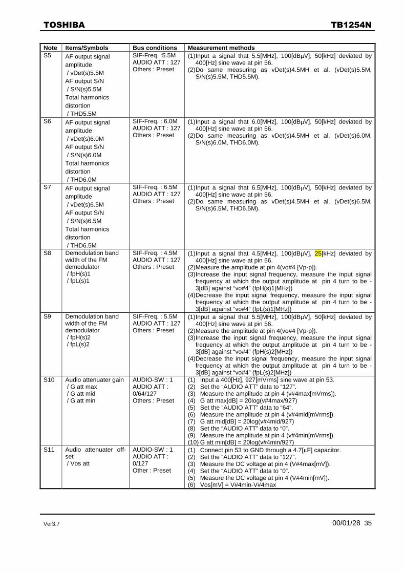
Note Items/Symbols Bus conditions Measurement methodsS5 AF output signal
amplitude / vDet(s)5.5MAF output S/N / S/N(s)5.5MTotal harmonicsdistortion / THD5.5M
SIF-Freq. :5.5MAUDIO ATT : 127Others : Preset
(1) Input a signal that 5.5[MHz], 100[dB�V], 50[kHz] deviated by400[Hz] sine wave at pin 56.
(2) Do same measuring as vDet(s)4.5MH et al. (vDet(s)5.5M,S/N(s)5.5M, THD5.5M).
S6 AF output signalamplitude / vDet(s)6.0MAF output S/N / S/N(s)6.0MTotal harmonicsdistortion / THD6.0M
SIF-Freq. : 6.0MAUDIO ATT : 127Others : Preset
(1) Input a signal that 6.0[MHz], 100[dB�V], 50[kHz] deviated by400[Hz] sine wave at pin 56.
(2) Do same measuring as vDet(s)4.5MH et al. (vDet(s)6.0M,S/N(s)6.0M, THD6.0M).
S7 AF output signalamplitude / vDet(s)6.5MAF output S/N / S/N(s)6.5MTotal harmonicsdistortion / THD6.5M
SIF-Freq. : 6.5MAUDIO ATT : 127Others : Preset
(1) Input a signal that 6.5[MHz], 100[dB�V], 50[kHz] deviated by400[Hz] sine wave at pin 56.
(2) Do same measuring as vDet(s)4.5MH et al. (vDet(s)6.5M,S/N(s)6.5M, THD6.5M).
S8 Demodulation bandwidth of the FMdemodulator / fpH(s)1 / fpL(s)1
SIF-Freq. : 4.5MAUDIO ATT : 127Others : Preset
(1) Input a signal that 4.5[MHz], 100[dB�V], 25[kHz] deviated by400[Hz] sine wave at pin 56.
(2) Measure the amplitude at pin 4(vo#4 [Vp-p]).(3) Increase the input signal frequency, measure the input signal
frequency at which the output amplitude at pin 4 turn to be -3[dB] against “vo#4” (fpH(s)1[MHz])
(4) Decrease the input signal frequency, measure the input signalfrequency at which the output amplitude at pin 4 turn to be -3[dB] against “vo#4” (fpL(s)1[MHz])
S9 Demodulation bandwidth of the FMdemodulator / fpH(s)2 / fpL(s)2
SIF-Freq. : 5.5MAUDIO ATT : 127Others : Preset
(1) Input a signal that 5.5[MHz], 100[dB�V], 50[kHz] deviated by400[Hz] sine wave at pin 56.
(2) Measure the amplitude at pin 4(vo#4 [Vp-p]).(3) Increase the input signal frequency, measure the input signal
frequency at which the output amplitude at pin 4 turn to be -3[dB] against “vo#4” (fpH(s)2[MHz])
(4) Decrease the input signal frequency, measure the input signalfrequency at which the output amplitude at pin 4 turn to be -3[dB] against “vo#4” (fpL(s)2[MHz])
S10 Audio attenuater gain / G att max / G att mid / G att min
AUDIO-SW : 1AUDIO ATT :0/64/127Others : Preset
(1) Input a 400[Hz], 927[mVrms] sine wave at pin 53.(2) Set the “AUDIO ATT” data to “127”.(3) Measure the amplitude at pin 4 (v#4max[mVrms]).(4) G att max[dB] = 20log(v#4max/927)(5) Set the “AUDIO ATT” data to “64”.(6) Measure the amplitude at pin 4 (v#4mid[mVrms]).(7) G att mid[dB] = 20log(v#4mid/927)(8) Set the “AUDIO ATT” data to “0”.(9) Measure the amplitude at pin 4 (v#4min[mVrms]).(10) G att min[dB] = 20log(v#4min/927)
S11 Audio attenuater off-set / Vos att
AUDIO-SW : 1AUDIO ATT :0/127Other : Preset
(1) Connect pin 53 to GND through a 4.7[�F] capacitor.(2) Set the “AUDIO ATT” data to “127”.(3) Measure the DC voltage at pin 4 (V#4max[mV]).(4) Set the “AUDIO ATT” data to “0”.(5) Measure the DC voltage at pin 4 (V#4min[mV]).(6) Vos[mV] = V#4min-V#4max

������� �����
Ver3.7 00/01/28 36
Note Items/Symbols Bus conditions Measurement methodsS12 Audio switch cross-
talk / CT(s)T-E / CT(s)E-T
SIF-Freq. : 5.5MAUDIO-SW : 0/1AUDIO ATT : 127Other : Preset
(1) Input a signal that 5.5[MHz], 100[dB�V], 50[kHz] deviated by1[kHz] sine wave at pin 56.
(2) Connect pin 53 to GND through a 4.7[�F] capacitor.(3) Measure level of the 1[kHz] at pin 4 (v#4T1[dB�V]).(4) Set the bit of “AUDIO-SW” to “1”.(5) Measure level of the 1[kHz] at pin 4 (v#4E1[dB�V]).(6) CT(s)T-E[dB] = v#4E1-v#4T1(7) Input a 5.5[MHz], 100[dB�V] signal at pin 56.(8) Measure level of the 1[kHz] at pin 4 (v#4E2[dB�V]).(9) Input a 1[kHz], 927[mVrms] signal at pin 53.(10) Set the bit of “AUDIO-SW” to “0”.(11) Measure level of the 1[kHz] at pin 4 (v#4T2[dB�V]).(12) CT(s)E-T[dB] = v#4T2-v#4E2
S13 Audio switch off-set / Vos sw
SIF-Freq. : 5.5MAUDIO-SW : 0/1AUDIO ATT : 127Other : Preset
(1) Input a 5.5[MHz], 100[dB�V] signal at pin 56.(2) Connect pin 53 to GND through a 4.7[�F] capacitor.(3) Set the bit of “AUDIO-SW” to “0”.(4) Measure the voltage at pin 4 (V#4T[V]).(5) Set the bit of “AUDIO-SW” to “1”.(6) Measure the voltage at pin 4 (V#E[V]).(7) Vos sw[V] = V#4E-V#4T
������� �����
Ver3.7 00/01/28 37
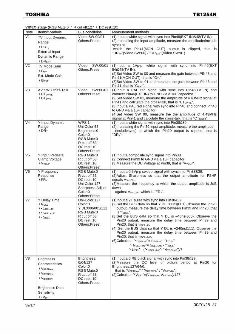
VIDEO stage (RGB Mute:0 / R cut off:127 / DC rest.:10)Note Items/Symbols Bus conditoins Measurement methodsV1 TV Input Dynamic
Range / DRTV
External InputDynamic Range / DREXT
Video SW:00/01Others:Preset
(1)Input a white signal with sync into Pin46(EXT IN)&48(TV IN).(2)Increasing the input amplitude, measure the amplitude(includesync) at which the Pin41(MON OUT) output is clipped, that is"DRTV"(Video SW:00) / "DREXT"(Video SW:01).
V2 TV Mode Gain / GTV
Ext. Mode Gain / GEXT
Video SW:00/01Others:Preset
(1)Input a 1Vp-p, white signal with sync into Pin46(EXTIN)&48(TV IN).(2)Set Video SW to 00 and measure the gain between PIN48 andPin41(MON OUT), that is "GTV".(3)Set Video SW to 01 and measure the gain between Pin46 andPin41, that is "GEXT".
V3 AV SW Cross-Talk / CTSWTE
/ CTSWET
Video SW:00/01Others:Preset
(1)Input a PAL red signal with sync into Pin48(TV IN) andconnect Pin46(EXT IN) to GND via a 1uF capacitor.(2)Set Video SW 01, measure the amplitude of 4.43MHz signal atPin41 and calculate the cross-talk, that is "CTSWTE".(3)Input a PAL red signal with sync into Pin46 and connect Pin48to GND via a 1uF capacitor.(4)Set Video SW 00, measure the the amplitude of 4.43MHzsignal at Pin41 and calculate the cross-talk, that is "CTSWET".
V4 Y Input DynamicRange / DRY
WPS:1Uni-Color:63Brightness:0Color:0RGB Mute:0R cut off:63DC rest.:10Others:Preset
(1)Input a white signal with sync into Pin38&39.(2)Increasing the Pin39 input amplitude, measure the amplitude (includesync) at which the Pin20 output is clipped, that is"DRY".
V5 Y Input PedestalClamp Voltage / VYCLP
RGB Mute:0R cut off:63DC rest.:10Others:Preset
(1)Input a composite sync signal into Pin38.(2)Connect Pin39 to GND via a 1uF capacitor.(3)Measure the DC Voltage at Pin39, that is "VYCLP".
V6 Y FrequencyResponse / FRY
RGB Mute:0R cut off:63DC rest.:10Uni-Color:127Sharpness:AdjustColor:0Others:Preset
(1)Input a 0.5Vp-p sweep signal with sync into Pin38&39.(2)Adjust Sharpness so that the output amplitude for FSHPequals VSH100k.(3)Measure the frequency at which the output amplitude is 3dBdown against VSH100k, which is "FRY".
V7 Y Delay Time / tYDEL
/ •tYDEL-40
/ •tYDEL+240
/ •tYDEL
Uni-Color:127Color:0Y DL:000/001/111RGB Mute:0R cut off:63DC rest.:10Others:Preset
(1) Input a 2T pulse with sync into Pin38&39.(2) Set the BUS data so that Y DL is 0ns(001).Observe the Pin20
output, measure the delay time between Pin39 and Pin20, thatis "tYDEL".
(3) Set the BUS data so that Y DL is –40ns(000). Observe thePin20 output, measure the delay time between Pin39 andPin20, that is tYDEL-40.
(4) Set the BUS data so that Y DL is +240ns(111). Observe thePin20 output, measure the delay time between Pin39 andPin20, that is tYDEL+240.
(5)Calculate, “•tYDEL-40”= tYDEL-40 - "tYDEL" “•tYDEL+240”= tYDEL+240 - "tYDEL"“•tYDEL”= (“•tYDEL+240”- “•tYDEL-40”)/7
V8 BrightnessCharacteristics / VBRTMAX
/ VBRTCEN
/ VBRTMIN
Brightness DataSensitivity / •VBRT
Brightness:0/64/127Color:0RGB Mute:0R cut off:63DC rest.:10Others:Preset
(1)Input a 0IRE black signal with sync into Pin38&39.(2)Measure the DC level of picture period at Pin20 forBrightness:127/64/0, that is "VBRTMAX" / "VBRTCEN" / "VBRTMIN".(3)Calculate;"•VBRT"=(VBRTMAX-VBRTMIN)/127

������� �����
Ver3.7 00/01/28 38
Note Items/Symbols Bus conditoins Measurement methodsV9 Uni-Color
Characteristics for Y / GUCYMAX
/ GUCYCEN
/ GUCYMIN
Uni-Color:0/64/127Color:0RGB Mute:0R cut off:63DC rest.:10Others:Preset
(1)Input a 50IRE white signal with sync into Pin38&39.(2)Measure the output picture amplitude at Pin20 for Uni-Color:127/64/0, that is VUCYMAX / VUCYCEN / VUCYMIN.(3)Calculate; "GUCYMAX"=20*log(VUCYMAX/0.357)" "GUCYCEN"=20*log(VUCYCEN/0.357) "GUCYMIN"=20*log(VUCYMIN/0.357)
V10 Sub-ContrastCharacteristics / GSCONMAX
/ GSCONMIN
Sub-Contrast:0/8/15Uni-Color:127Color:0RGB Mute:0R cut off:63DC rest.:10Others:Preset
(1)Input a 50IRE white signal with sync into Pin38&39.(2)Measure the output picture amplitude at Pin20 for Sub-Contrast 15/8/0, that is VSCONMAX / VSCONCEN / VSCONMIN.(3)Calculate; "GSCONMAX"=20*log(VSCONMAX/VSCONCEN) "GSCONMIN"=20*log(VSCONMIN/VSCONCEN)
V11 Sharpness PeakingFrequency / FSHP
Sharpness:63Uni-Color:127Color:0RGB Mute:0R cut off:63DC rest.:10Others:Preset
(1)Input a 0.5Vp-p sweep signal with sync into Pin38&39.(2)Measure the frequency at which the Pin20 output amplitude isMax., that is "FSHP".
V12 Sharpness ControlCharacteristics / GSHMAX / GSHCEN / GSHMIN
Sharpness:0/32/63 Uni-Color:127Color:0RGB Mute:0R cut off:63DC rest.:10Others:Preset
(1)Input a 0.5Vp-p sweep signal with sync into Pin38&39.(2)Measure the output picture amplitude for 100kHz at Pin20, thatis VSH100k.(3)Measure the output picture amplitude for FSHP whenSharpness is max.,center and min., that is VSHMAX, VSHCEN andVSHMIN.(4)Calculate; "GSHMAX"=20*log(VSHMAX/VSH100k) "GSHCEN"=20*log(VSHCEN/VSH100k) "GSHMIN"=20*log(VSHMIN/VSH100k)
V13 Y • correction startpoint / VY• 70
/ VY• 80
/ VY• 90
Y • correction curve / GY•
Uni-Color:127Color:0RGB Mute:0R cut off:63DC rest.:10• point:01/10/11Others:Preset
(1) Input a gray raster with sync to Pin38&39.(2) Set BUS data so that • point is 90IRE.(3) Increasing a video amplitude of input from 50IRE, measure a
video ampitude as the figure below, that is “VY• 90”(4) Set BUS data so that • point is 80IRE.And repeat (3), that is
“VY• 80”.(5) Set BUS data so that • point is 70IRE.And repeat (3), that is
“VY• 70”.(6) From the measurement in the above, find gain of the portion
that the • correction has an effect on.
Y ƒÁ=off
Y ƒÁ=90/80/70IRE
#39 input
#20output
VYƒÁ90

������� �����
Ver3.7 00/01/28 39
Note Items/Symbols Bus conditoins Measurement methodsV14 Black Expansion Start
Point / VBLEX25
/ VBLEX35
/ VBLEX45
Black Expansion AMPGain / GBLEX
Uni-Color:127Color:0Blackstretch:00/01 /10/11RGB Mute:0R cut off:63DC rest.:10Others:Preset
(1) Input a gray raster with sync to Pin38&39.(2) Set black stretch to 25IRE.(3) Decreasing Y amplitude of input from 50IRE, measure a Y
amplitude as the figure below, that is “VBLEX25”(4) Set black stretch to 35IRE/45IRE.(5) Repeat (3), that is ‘VBLEX35”, “VBLEX45”. below, that is “VY• 90”(6) Find gain of the portion that the black stretch has an effect on.
Blackstretch
=off
25/35/45IRE
#39 input
#20output
VBLEX25
V16 DC Restration Gain / VDcrest120
/ VDcrest90
/ VDcrest step
Uni-Color:127Color:0Blackstretch:00/01 /10/11RGB Mute:0R cut off:63DC rest.:10Others:Preset
(1) Input a 100IRE signal with sync into Pin38&39.(2) Set DC rest. to 10.(3) Measure a Y amplitude of pin20 output, that is V100.(4) Set DC rest to 00.(5) Measure a Y amplitude of pin20 output, that is V120.(6) Calculate, “Vdcrest120” =(V120/V100)×100(7) Set DC rest to 11.(8) Repeat (5)&(6), that is “VDcrest90”.(9) Calculate, “VDcrest step”=(Vdcrest120 - VDcrest90)/4
V17 WPS Level / VWPS
Uni-Color:127Brightness:127Color:0RGB Mute:0R cut off:63DC rest.:10Others:Preset
(1)Input a 120IRE ramp signal with sync into Pin38&39.(2)Measure the amplitude from cut-off level to peak(at whichoutput signal is clipped), that is "VWPS".
V18 Chroma Trap Gain / GTRAP
C-Trap:0/1Uni-Color:127Color:0RGB Mute:0R cut off:63DC rest.:10Others:Preset
(1)Input a 0.5Vp-p, 3.58MHz signal with sync into Pin43&39.(2)Measure the 3.58MHz amplitude at PIn20 for ChromaTrap:1/0, that is VTRAPON / VTRAPOFF.(3)Calculate;"GTRAP"=20*log(VTRAPON/VTRAPOFF)
V19 Half ToneCharacteristics for Y / GHTY
Ysm Mode:0Uni-Color:127Color:0RGB Mute:0R cut off:63DC rest.:10Others:Preset
(1)Input a 100IRE white signal with sync into Pin38&39.(2)Measure the output picture amplitude at PIn20 , that isVHTYOFF.(3)Suppry Pin15 2V.(4) Measure the output picture amplitude at PIn20 , that is VHTYON
.(3)Calculate;"GHTY"=20*log(VHTYON/VHTYOFF)
������� �����
Ver3.7 00/01/28 40
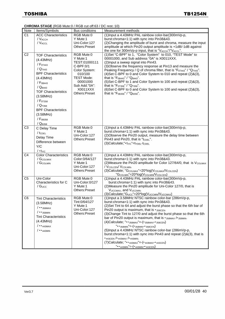
CHROMA STAGE (RGB Mute:0 / RGB cut off:63 / DC rest.:10)Note Items/Symbols Bus conditoins Measurement methodsC1 ACC Characteristics
/ VACCH
/ VACCL
RGB Mute:0Y Mute:1Uni-Color:127Others:Preset
(1)Input a 4.43MHz PAL rainbow color-bar(300mVp-p,burst:chroma=1:1) with sync into Pin38&43.(2)Changing the amplitude of burst and chroma, measure the inputamplitude at which Pin20 output amplitude is +1dB/-1dB againstthe one for 300mVp-p input, that is "VACCH"/"VACCL".
C2 TOF Characteristics(4.43MHz) / F0T443
/ QT443
BPF Characteristics(4.43MHz) / F0B443
/ QB443
TOF Characteristics(3.58MHz) / F0T358
/ QT358
BPF Characteristics(3.58MHz) / F0B358
/ QB358
RGB Mute:0Y Mute:1TEST:01000111C-BPF:0/1Color System: 010/100TEST Mode: 00001000Sub Add.”0A”: X0011XXXOthers:Preset
(1)Set “C-BPF” to 1, “Color System” to 010, “TEST Mode” to00001000, and Sub address “0A” is X0011XXX.(2)Input a sweep signal into Pin43.(3)Observe the frequency response at Pin13 and measure thePeaking Frequency / Q of chroma filter, that is "F0T443" / "QT443".(4)Set C-BPF to 0 and Color System to 010 and repeat (2)&(3),that is "F0B443" / "QB443".(5)Set C-BPF to 1 and Color System to 100 and repeat (2)&(3),that is "F0T358" / "QT358".(6)Set C-BPF to 0 and Color System to 100 and repeat (2)&(3),that is "F0B358" / "QB358".
C3 C Delay Time / tCDEL
Delay TimeDifference betweenY/C / •tY/C
RGB Mute:0Y Mute:1Uni-Color:127Others:Preset
(1)Input a 4.43MHz PAL rainbow color-bar(300mVp-p,burst:chroma=1:1) with sync into Pin38&43.(2)Observe the Pin20 output, measure the delay time betweenPin43 and Pin20, that is "tCDEL".(3)Calculate;"•tY/C"=tYDEL-tCDEL
C4 Color Characteristics / GCOLMAX
/ GCOLMIN
RGB Mute:0Color:0/64/127Y Mute:1Uni-Color:127Others:Preset
(1)Input a 4.43MHz PAL rainbow color-bar(300mVp-p,burst:chroma=1:1) with sync into Pin38&43.(2)Measure the Pin20 amplitude for Color 127/64/0, that is VCOLMAX
/ VCOLCEN/ VCOLMIN.(3)Calculate; "GCOLMAX"=20*log(VCOLMAX/VCOLCEN) "GCOLMIN"=20*log(VCOLMIN/VCOLCEN)
C5 Uni-ColorCharacteristics for C / GUCC
RGB Mute:0Uni-Color:0/127Y Mute:1Others:Preset
(1) Input a 4.43MHz PAL rainbow color-bar(300mVp-p,burst:chroma=1:1) with sync into Pin38&43.
(2) Measure the Pin20 amplitude for Uni-Color 127/0, that isVUCCMAX, and VUCCMIN.
(3) Calculate;"GUCC"=20*log(VUCCMIN/VUCCMAX)C6 Tint Characteristics
(3.58MHz) / ••358MAX
/ ••358MIN
Tint Characteristics(4.43MHz) / ••443MAX
/ ••443MIN
RGB Mute:0Tint:0/64/127Y Mute:1Uni-Color:127Others:Preset
(1)Input a 3.58MHz NTSC rainbow color-bar (286mVp-p,burst:chroma=1:1) with sync into Pin38&43.(2)Set Tint to 64 and adjust the burst phase so that the 6th bar ofPin20 output is maximum, that is •358CEN.(3)Change Tint to 127/0 and adjust the burst phase so that the 6thbar of Pin20 output is maximum, that is •358MAX /•358MIN.(4)Calculate; "••358MAX"=-(•358MAX-•358CEN) "••358MIN"=-(•358MIN-•358CEN)(5)Input a 4.43MHz NTSC rainbow color-bar (286mVp-p,burst:chroma=1:1) with sync into Pin43 and repeat (2)&(3), that is•443CEN /•443MAX /•443MIN.(7)Calculate; "••443MAX"=-(•443MAX-•443CEN) "••443MIN"=-(•443MIN-•443CEN)
������� �����
Ver3.7 00/01/28 41
Note Items/Symbols Bus conditoins Measurement methodsC7 Relative Amplitude
(PAL) / VPR/B
/ VPG/B
Relative Amplitude(NTSC1) / VN1R/B
/ VN1G/B
Relative Amplitude(NTSC2) / VN2R/B
/ VN2G/B
Relative Amplitude(DVD) / VDR/B
/ VDG/B
RGB Mute:0Y Mute:1Uni-Color:127Others:Preset
(1) Input a 4.43MHz PAL rainbow color-bar(300mVp-p,burst:chroma=1:1) with sync into Pin38&43.
(2) Measure the amplitude of Pin18/19/20 output, that is"VPROUT"/ "VPGOUT" / "VPBOUT"
(3) Calculate; " VPR/B "=VPROUT/VPBOUT " VPG/B "=VPGOUT/VPBOUT(4) Input a 3.58MHz NTSC rainbow color-bar (286mVp-p,
burst:chroma=1:1) with sync into Pin38&43.(5) Set NTSC Phase to NTSC1/NTSC2.(6) Repeat (2)&(3), that is “VN1R/B”/” VN1G/B”/” VN2R/B”/” VN2G/B”.
C8 Relative Phase (PAL) / •PR-B
/ •PG-B
Relative Phase(NTSC1) / •N1R-B
/ •N1G-B
Relative Phase(NTSC2) / •N2R-B
/ •N2G-B
Relative Phase (DVD) / •DR-B
/ •DG-B
RGB Mute:0Y Mute:01Uni-Color:127NTSC Phase: 00/01/10Others:Preset
(1)Input a 4.43MHz PAL rainbow color-bar(300mVp-p,burst:chroma=1:1) with sync into Pin38&43.(2)Observe the Pin18/19/20 output, measure the R/G/B modulationangle (•PR/•PG/•PB) accoeding following figure and equality. For •PR ; Peak:3rd bar, •0R=90 For •PG ; Peak(nagative):4th bar, •0G=240 For •PB ; Peak:6th bar, •0B=0Calculate; "•PR-B"=•PR-•PB
"•PG-B"=•PG-•PB
(4)Set NTSC Phase 00(NTSC1).(5)Input a 3.58MHz NTSC rainbow color-bar (286mVp-p,burst:chroma=1:1) with sync into Pin38&43, then repeat (2), that is•N1R /•N1G /•N1B.(6)Calculate; "•N1R-B"=•N1R-•N1B
"•N1G-B"=•N1G-•N1B
(7)Set NTSC Phase 01(NTSC2).(8) Repeat (5), that is •N2R /•N2G /•N2B.(9)Calculate; "•N2R-B"=•N2R-•N2B
"•N1G-B"=•N1G-•N1B
(10)Set NTSC Phase 10(DVD).
C9 APC Pull-in Range(4.43MHz) / •F4APCP+
/ •F4APCP-
APC Hold Range(4.43MHz)/ •F4APCH+
/ •F4APCH-
APC Pull-in Range(3.58MHz)/ •F3APCP+
/ •F3APCP-
APC Hold Range(3.58MHz)/ •F3APCH+
/ •F3APCH-
RGB Mute:0Color System:100/010Others:Preset
(1)Input a 4.43MHz PAL rainbow color-bar(300mVp-p,burst:chroma=1:1) with sync into Pin38&43.(2)Set Color System to 100(443PAL).(3)For higher frequency than 4.43MHz, measure the burstfrequency at which Pin13 DC level changes from low to high / fromhigh to low, that is F4APCP+ / F4APCH+.(4)For lower frequency than 4.43MHz, repeat (2), that is F4APCP- /F4APCH-.(5)Calculate; "•F4APCP+"=F4APCP+-4433619 "•F4APCP-"=4433619-F4APCP-
"•F4APCH+"=F4APCH+-4433619 "•F4APCH-"=4433619-F4APCH-
(6)Input a 3.58MHz NTSC rainbow color-bar (286mVp-p,burst:chroma=1:1) with sync into Pin38&43.(7)Set Color System to 010(358NTSC).(8)For higher frequency than 3.58MHz, repeat (2), that is F3APCP+ /F3APCH+.(9)For lower frequency than 3.58MHz, repeat (2), that is F3APCP- /F3APCH-.(10)Calculate; "•F3APCP+"=F3APCP+-3579545 "•F3APCP-"=3579545-F3APCP-
"•F3APCH+"=F3APCH+-3579545 "•F3APCH-"=3579545-F3APCH-

������� �����
Ver3.7 00/01/28 42
Note Items/Symbols Bus conditoins Measurement methodsC10 APC Control
Sensitivity (4.43MHz) / •443
APC ControlSensitivity (3.58MHz) / •358
RGB Mute:0Color System:100/010Others:Preset
(1)Connect Pin43 to GND via a 1uF capacitor.(2)Set Color System to 100(443PAL).(3)Adjust Pin11 voltage so that the Pin13 output frequency is4.433619MHz, that is V4APCCEN.(4)Measure the Pin13 output frequency when Pin11 voltage is V4APCCEN+100mV / V4APCCEN-100mV, that is F4APC+ / F4APC-.(5)Calculate; "•443"=(F4APC+-F4APC-)/200(6)Set Color System to 010(358NTSC).(7)Adjust Pin11 voltage so that the Pin13 output frequency is3.579545MHz, that is V3APCCEN.(8)Measure the Pin13 output frequency when Pin11 voltage is V3APCCEN+100mV / V3APCCEN-100mV, that is F3APC+ / F3APC-.(9)Calculate; "•358"=(F3APC+-F3APC-)/200
C11 PAL ID Sensitivity(Normal Mode) / VPALIDON
/ VPALIDOFF
PAL ID Sensitivity(Low Mode) / VPALIDLON
/ VPALIDLOFF
NTSC ID Sensitivity(Normal Mode) / VNTIDON
/ VNTIDOFF
NTSC ID Sensitivity(Low Mode) / VNTIDLON
/ VNTIDLOFF
P/N ID Sens:0/1Color System:100/010Y Mute:01Uni-Color:127RGB Mute:0Others:Preset
(1)Set P/N ID Sens. to 0.(2)Set Color System to 100(443PAL).(3)Input a 4.43MHz PAL rainbow color-bar(300mVp-p,burst:chroma=1:1) with sync into Pin38&43.(4)Measure the burst amplitude at which Pin13 DC level changesfrom low to high / from high to low, that is "VPALIDON" / "VPALIDOFF".(5)Set Color System to 010(358NTSC).(6)Input a 3.58MHz NTSC rainbow color-bar (286mVp-p,burst:chroma=1:1) with sync into Pin38&43, and repeat (3), that is"VNTIDON" / "VNTIDOFF".(7)Set P/N ID Sens.to 1, repeat (2) ~ (6), that is "VPALIDLON" ,"VPALIDLOFF" , "VNTIDLON" and "VNTIDLOFF".
C12 fsc Continuous WaveOutput Level / VCW
RGB Mute:00Others:Preset
Measure the amplitude of Pin20 output, that is "VCW".
C13 Half ToneCharacteristics for C / GHTC
RGB Mute:0Ysm Mode:0Y Mute:01Uni-Color:127Others:Preset
(1)Input a 4.43MHz PAL rainbow color-bar(300mVp-p,burst:chroma=1:1) with sync into Pin38&43.(2)Supply Pin15 2V and measure the amplitude of Pin20 output,that is VPBHTC.(3)Calculate;"GHTC"=20*log(VPBHTC/VPBOUT)
C14 Sub-Color ControlCharacteristics / • SCOLMAX
/ • SCOLMIN
RGB Mute:00Y Mute:01Uni-Color:127Sub-Color:0/16/32Others:Preset
1)Input a signal(f0=100kHz,300mV) of following figure intoPin38,44&45.(2)Measure the Pin20 amplitude for Sub-olor 32/16/0, that isVSCMAX / VSCLCEN/VSCMIN.(3)Calculate; "• SCOLMAX "=20*log(VSCMAX / VSCLCEN) "• SCOLMIN "=20*log(VSCMIN / VSCLCEN)
Ampl i tude V0
Sinusoidal waveFrequency f 0
p in38 input
pin16 input

������� �����
Ver3.7 00/01/28 43
SECAM STAGENote Items/Symbols Bus conditoins Measurement methodsSE1 Bell Monitor output
voltage / embo
RGB Mute:0TEST Mode: 00001000Sub Add.”1A”: X0111XXXOthers:Preset
(1) Input a 75% color bar signal (200mVp-p at R ID) into Pin43.(2) Set BUS data so that “(3) TEST Mode” is 00001000 and Sub address “0A” is X0111XXX.(3) Measure R-Y ID amplitude at Pin13, that is "ebmo".
SE2 Bell filter f0 / f0B-C
RGB Mute:00TEST Mode: 00001000Sub Add.”0A”: X0111XXXBell f0:0Y Mute:1Others:Preset
(1) Input a 20mVp-p sine wave whose frequency is sweep intoPin43.
(2) Set BUS data so that “TEST Mode” is 00001000 and Subaddress “0A” is X0111XXX.
(3) Measure the frequency at which Pin13 output is the biggest,that is "f0BEL" .
(4) Calculate : "f0B-C"=f0BEL-4,286 [kHz].
SE3 Bell filter f0 variablerange / f0B-VR
RGB Mute:00TEST Mode: 00001000Sub Add.”0A”: X0111XXXBell f0:1Y Mute:1Others:Preset
(1) Input a 20mVp-p sine wave whose frequency is sweep intoPin43.
(2) Set BUS data so that “TEST Mode” is 00001000 and Subaddress “0A” is X0111XXX.
(3) Set BUS data so that “Bell f0” is +35kHz.(4) Measure the frequency at which Pin 13 output is the biggest,
that is f0BELH.(5) Calculate : " f0B-VR "= f0BELH -4,286 [kHz]
SE4 Bell filter Q / QBEL
RGB Mute:00TEST Mode: 00001000Sub Add.”0A”: X0111XXXY Mute:1Others:Preset
(1)Input a 20mVp-p sine wave whose frequency is sweep intoPin43.(2)Set BUS data so that “TEST Mode” is 00001000 and Subaddress “0A” is X0111XXX.(4) Observe the frequency response of Pin13 output.(5) Calculate : "QBEL = (MAX-3dB Band Width)/f0BEL.
SE5 Color differenceoutput amplitude / VBS / VRS
RGB Mute:00Uni-Color:63Y Mute:1Others:preset
(1) Input a 75% color bar(200mVp-p at R ID) into Pin43.(2) Measure the R-Y output amplitude at Pin20, that is "VRS".(3) Measure the B-Y output amplitude at Pin22, that is "VBS".
SE6 Color DifferenceRelative Amplitude / R/B-S
(1)Calculate : "R/B-S"=VRS/VBS
SE8 Color Difference S/NRatio / SNB-S / SBR-S
RGB Mute:00Uni-Color:63Y Mute:1Others:preset
(1) Input a 200mVp-p non-modulated chroma signal into Pin43.(2) Measure the amplitude of noise on Pin20, that is nR.(3) Measure the amplitude of noise on Pin22, that is nB.(4) Calculate : "SNB-S"=20log(2• 2VBS/nB) "SNR-S"=20log(2• 2VRS/nR)

������� �����
Ver3.7 00/01/28 44
Note Items/Symbols Bus conditoins Measurement methodsSE9 Linearity
/ LinB / LinR
RGB Mute:00Uni-Color:63Y Mute:1Others:preset
(1) Input a 75% color bar(200mVp-p at R ID) into Pin43.(2) Set BUS data so that “S black monitor” is “alignment”.(2) Measure the amplitude between Black and Cyan/Red, that isVCyan/VRed.(3) Measure the amplitude between Black and Yellow/Blue, that isVYellow/VBlue.(4) Calculate : "LinR"=VCync/VRed "LinB"=VYellow/VBlue
LinR
LinB
red
cyanblue
yellow
SE10 Rising-Fall Time / trfB / trfR
RGB Mute:00Uni-Color:63Y Mute:1Others:preset
(1) Input a 75% color bar(200mVp-p at R ID) into Pin43.(2) Set BUS data so that “S black monitor” is “alignment”.(3) Measure the rising time(from 10% to 90%) between Green and
Magenta at Pin 20/Pin 22, that is "trR"/"trB".Magenta
Green 10% 90%
trB•CtrR
SE11 SECAM ID Sensitivity(Normal Mode) / VSIDHON
/ VSIDHOFF
/ VSIDHVON
/ VSIDHVOFF
SECAM ID Sensitivity(Low Mode) / VSIDLHON
/ VSIDLHOFF
/ VSIDLHVON
/ VSIDLHVOFF
RGB Mute:00Y Mute:1S ID Sens:0/1S ID Mode:0/1ColorSystem:101Others:Preset
(1) Input a 75% color bar(200mVp-p at R ID) into Pin43.(2) Set BUS data so that “S ID Sens” is Normal, “S ID Mode” is H.(3) Measure the burst amplitude at which Pin13 DC level changes
from low to high / from high to low, that is "VSIDHON" / "VSIDHOFF".(4) Set BUS data so that “S ID Mode” is H+V.(5) Repeat (3), that is "VSIDHVON" / "VSIDHVOFF".(6) Set BUS data so that “S ID Sens” is Low, “S ID Mode” is H.(7) Repeat (3), that is "VSIDLHON" / "VSIDLHOFF".(8) Set BUS data so that “S ID Mode” is H+V.(9) Repeat (3), that is "VSIDLHVON" / "VSIDLHVOFF".
SE12 Gate Pulse WidthVariable Range / WGP+200
/ WGP / WGP-200
RGB Mute:00TEST Mode: 00001000Sub Add.”0A”: X1001XXXColorSystem:101Others:Preset
(1) Input a 75% color bar(200mVp-p at R ID) into Pin43.(2) Set BUS data so that “TEST Mode” is 00001000 , Sub address
“0A” is X1001XXX , and“Color System” is Fixed SECAM.(3) Measure the gate pulse widths when BUS data of “SECAM GP
Phase” is +200ns / normal / -200ns, those are “WGP+200”,“WGP” and “WGP-200”.
S13 SECAM blackadjustmentcharacteristic / VSBMAX
/ VSRMAX
/ VSRMIN
/ VSRMIN
SECAM blackadjustment sensitivity /• VSB
/• VSR
RGB Mute:00ColorSystem:101S black Monitor:1S B-Y black Adj.: 0/15S R-Y black Adj.: 0/15Others:Preset
(1)For B-Y/R-Y Black Adj.:8, measure the DC level of picture periodat Pin22/20, that is VSBCEN / VSRCEN.
(3)For B-Y Black Adj.:0/15, measure the DC level change of pictureperiod against VSBCEN at Pin22, that is "VSBMIN" / "VSBMAX".
(4)For R-Y Black Adj.:0/15, measure the DC level change of pictureperiod against VSRCEN at Pin20, that is "VSRMIN" / "VSRMAX".
(5)Calculate;"• VSECB"=(VSBMAX-VSBMIN)/16
"• VSECR"=(VSECRMAX-VSECRMIN)/16

������� �����
Ver3.7 00/01/28 45
TEXT STAGE(RGB Mute:0 / RGB cut off:63 / DC rest.:10)Note Items/Symbols Bus conditoins Measurement methodsT1 V-BLK Pulse Output
Level / VVBLK
H-BLK Pulse OutputLevel
/ VHBLK
All:Preset (1)Input a cmposite sync signal into Pin38.(2)Measure the DC level of V/H blanking period at Pin20, that is "VVBLK" / "VHBLK".
T2 RGB Output BlackLevel (0IRE DC) / VBLACK
RGB Mute:0Color:0R cut off:63DC rest.:10Others:Preset
(1)Input a 0IRE Y signal with sync into Pin38&39.(2)Measure the DC level of picture period at Pin20, that is "VBLACK".
T3 RGB Output WhiteLevel(100 IRE AC) / VWHITE
RGB Mute:0R cut off:63DC rest.:10Uni-Color:127Color:0Others:Preset
(1)Input a 100IRE Y signal with sync into Pin38&39.(2)Measure the amplitude from 0 to 100IRE at Pin20, that is"VWHITE".
T4 Cut-off VoltageVariable Range / •VCUT+
/ •VCUT-
RGB Mute:0DC rest.:10B Cut Off:0/255Color:0Others:Preset
(1)Input a 0IRE Y signal with sync into Pin38&39.(2)Measure the DC level of picture period at Pin22 for B Cut-off:255/0 , that is VCUTMAX / VCUTMIN.(3)Calculate; "•VCUT+"=VCUTMAX-VBLACK "•VCUT-"=VCUTMIN-VBLACK
T5 Drive Control VariableRange / GDR+
/ GDR-
RGB Mute:0DC rest:10B Drive:0/127Uni-Color:127Color:0Others:Preset
(1)Input a 100IRE Y signal with sync into Pin38&39.(2)Measure the amplitude from 0 to 100IRE at Pin20 for Bdrive127/0, that is VDRMAX / VDRMIN.(1) Calculate; "GDR+"=20*log(VDRMAX/VWHITE) "GDR-"=20*log(VDRMIN/VWHITE)
T6 ABCL ContorolVoltage Range / VABCLH
/ VABCLL
ACL Gain
/ GACL
RGB Mute:0R cut off:63DC rest.:10ABL Gain:11Uni-Color:127Color:0Others:Preset
(1)Input a 100IRE Y signal with sync into Pin38&39.(2)Decreasing the Pin28 voltage, measure the voltage at whichPin20 output begins/stops decreasing, that is "VABCLH" / "VABCLL".(3)Measure the minimum amplitude of Pin20 output, that is VACLMIN.(4)Calculate; "GACL"=20*log(VACLMIN/VWHITE)
T7 ABL Start Point / VABLP0
/ VABLP1
/ VABLP2
/ VABLP3
RGB Mute:0R cut off:63DC rest.:10ABL Start Point: 00/01/10/11ABL Gain:11Uni-Color:127Color:0Others:Preset
(1)Input a 0IRE Y signal with sync into Pin38&39.(2)For ABL Point 00/01/10/11, decreasing the Pin28 voltage,measure the voltage at which Pin20 output begins decreasing, that is VABL1/VABL2/VABL3/VABL4.(3)Calculate; "VABLP0"=VABL1-VABCLH
"VABLP1"=VABL2-VABCLH
"VABLP2"=VABL3-VABCLH
"VABLP3"=VABL4-VABCLH
T8 ABL Gain / VABLG0
/ VABLG1
/ VABLG2
/ VABLG3
RGB Mute:0R cut off:63DC rest.:10ABL Gain: 00/01/10/11Uni-Color:127Color:0Others:Preset
(1)Input a 0IRE Y signal with sync into Pin38&39.(2)For ABL Gain 00/01/10/11, measure the DC level of pictureperiod at Pin20 when Pin28 voltage is VABCLL, that isVABL5/VABL6/VABL7/VABL8.(3)Calculate; "VABLG0"=VABL5-VBLACK
"VABLG1"=VABL6-VBLACK
"VABLG2"=VABL7-VBLACK
"VABLG3"=VABL8-VBLACK

������� �����
Ver3.7 00/01/28 46
Note Items/Symbols Bus conditoins Measurement methodsT9 Analog RGB Dynamic
Range / DRTX
RGB Mute:0R cut off:63DC rest.:10RGB Contrast:32Ysm Mode:1Others:Preset
(1)Input a composite sync signal into Pin38.(2)Supply 2V to Pin15.(3)Input a signal of following figure into Pin16.(4)Increasing the amplitude of Pin16 input, measure the amplitudeat which the Pin20 amplitude stops increasing, that is "DRTX".
Ampl i tude V0
Sinusoidal waveFrequency f 0
p in38 input
pin16 input
T10 Analog RGB ContrastControl Characteristic / GTXCMAX
/ GTXCCEN
/ GTXCMIN
RGB Mute:0R cut off:63DC rest.:10Ysm Mode:1RGB Contrast:0/32/63Others:Preset
(1)Input a cmposite sync signal into Pin38.(2)Supply 2V to Pin15.(3)Input a signal of NOTE:T9 figure(f0=100kHz,V0=0.2Vp-p) intoPin16.(4)For RGB Contrast 63/32/0, measure the amplitude of Pin20output, that is VTXCMAX / VTXCCEN / VTXCMIN.(5)Calculate; "GTXCMAX"=20*log(VTXCMAX/0.2) "GTXCCEN"=20*log(VTXCCEN/0.2) "GTXCMIN"=20*log(VTXCMIN/0.2)
T11 Analog RGBBrightness ControlCharacteristic / VTXBRMAX
/ VTXBRCEN
/ VTXBRMIN
RGB Mute:0R cut off:63DC rest.:10Ysm Mode:1Brightness:0/64/127Others:Preset
(1)Supply 2V to Pin15.(2)Connect Pin16 to GND via a 0.1uF capacitor.(3)For Brightness 127/64/0, measure the DC level of picture periodat Pin20, that is "VTXBRMAX" / "VTXBRCEN" / "VTXBRMIN".
T12 Analog RGB ModeSwitching Level / VYS
RGB Mute:0Ysm Mode:1RGB Contrast:32Others:Preset
(1)Input a cmposite sync signal into Pin38.(2)Input a signal of NOTE:T9 figure into Pin16.(3)Increasing the Pin15 voltage, measure the voltage at which thesignal inputted into Pin16 appears at Pin20, that is "VYS".
T13 Analog RGB ModeTransferCharacteristic / •RYS
/ tPRYS
/ •FYS
/ tPFYS
RGB Mute:0R cut off:63DC rest.:10Ysm Mode:1Others:Preset
(1)Input a 50IRE Y singnal with sync into Pin38&39.(2)Connect Pin16 to GND via a 0.1uF capacitor.(3)According to following figure, measure the Analog RGB ModeTransfer Characteristic.
1H
20ƒÊs
20ƒÊs
20ns20ns
tPR YS tPF YS
50%
100%
0%
50%90%
10%
ĄR YS ĄF YS
Pin15 Input
Pin20 Output

������� �����
Ver3.7 00/01/28 47
Note Items/Symbols Bus conditoins Measurement methodsT14 Cross Talk from
Analog RGB to TV / CTTX-TV
RGB Mute:0R cut off:63DC rest.:10Ysm Mode:1Uni-color:127RGB contrast:63Others:Preset
(1) Input a composite sync signal into Pin38.(2) Connect Pin39 to GND via a 1uF capacitor.(3) Input a sine wave signal (f=4MHz, Video amplitude=0.5Vp-p)
into Pin16.(4) Supply 0V to Pin15.(5) Measure the amplitude at Pin20, that is VTV.(6) Supply 2V to Pin15.(7) Measure the amplitude of 4MHz signal at Pin20, that is VTX.(8) (8)Calculate;"CTTX-TV"=20*log(VTV/ VTX)
T15 Cross Talk from TV toAnalog RGB / CTTV-TX
RGB Mute:0R cut off:63DC rest.:10Ysm Mode:1Uni-color:127RGB contrast:63Others:Preset
(1) Input a sine wave signal (f=4MHz, Video amplitude=0.5Vp-p)with sync into Pin38&39.
(2) Connect Pin16 to GND via a 0.1uF capacitor.(3) Supply 2V to Pin15.(4) Measure the amplitude at Pin20, that is VTX.(5) Supply 0V to Pin15.(6) Measure the amplitude of 4MHz signal at Pin20, that is VTV.(7) Calculate;"CTTV-TX"=20*log(VTX/ VTV)
T16 SECAM Black LevelAdj. Characteristics / VSECBMAX
/ VSECRMAX
/ VSECBMIN
/ VSECRMIN
SECAM Black LevelAdj. Data Sensitivity / •VSECB
/ •VSECR
RGB Mute:0R cut off:63DC rest.:10ColorSystem:111 B-YBlack Adj: 0/8/15R-Y Black Adj: 0/8/15S black monitor:1Others:Preset
(1) Set S black monitor to 1.(2)For B-Y/R-Y Black Adj.:8, measure the DC level of picture periodat Pin22/20, that is VSECBCEN / VSECRCEN.(3)For B-Y Black Adj.:0/15, measure the DC level change of pictureperiod against VSECBCEN at Pin22, that is "VSECBMIN" / "VSECBMAX".(4)For R-Y Black Adj.:0/15, measure the DC level change of pictureperiod against VSECRCEN at Pin20, that is "VSECRMIN" / "VSECRMAX".(5)Calculate; "•VSECB"=(VSECBMAX-VSECBMIN)/16 "•VSECR"=(VSECRMAX-VSECRMIN)/16
T17 Base band TINTcharacteristic / •• BBMAX
/ •• BBMIN
RGB Mute:0R cut off:63DC rest.:10Uni-color:127Others:Preset
(1) Input a signal(f0=100kHz, 100mVp-p) of NOTE T9 intoPin44&38.
(2) Into Pin45, into a signal with the same amplitude but 90degphase advanced compared to the signal input to pin44.
(3) When baseband TINT is changed ‘10000’ to“00000”, measurethe amount of change in the output phase of Pin20, that is“•• BBMIN”.
(4) When baseband TINT is changed ‘10000’ to“11111”, measurethe amount of change in the output phase of Pin20, that is“•• BBMIN”.
T18 Analog RGB•RGBOutput Voltage AxesDifference••VR-G
••VG-B
••VB-R
RGB Mute:0R/G/B cut off:63Brightness:63DC rest.:10Color:0Uni-color:127Others:Preset
(1)Input a 0IRE signal with sync into Pin38&39. (2)Connect Pin16,17,18 to GND via 0.01•F. (3)Measure the DC level of picture period at Pin20,21,22, that isRY/GY/BY.
(4)Supply Pin15 to 2V.(5) Measure the DC level of picture period at Pin20,21,22, that isRT/GT/BT.
(6)Calculate; •R • RT • RY
•G • GT • GY
•B • BT • BY
“•VR-G” • •R • •G “•VG-B” • •G • •B“•VB-R” • •B • •R
DEF STAGENote Items/Symbols Bus conditoins Measurement methodsD1 AFC Inactive Period
/ T50AFCOFF
/ T60AFCOFF
All:Preset (1)Input a 50Hz/60Hz composite sync signal into Pin38.(2)Measure "T50AFCOFF" / "T60AFCOFF" at Pin29. (cf. Fig.D1)

������� �����
Ver3.7 00/01/28 48
Note Items/Symbols Bus conditoins Measurement methodsD2 H-OUT Start Voltage
/ VHON
All:Preset (1)Let Pin1/14/37/42 be open.(2)Increasing Pin31 voltage, measure the voltage at which HOUT pulse appears at Pin32, that is "VHON".
D3 H-OUT Pulse Duty / WHOUT
All:Preset (1) Measure tHOUT1 & tHOUT2 at Pin32.(2) Calculate;"WHOUT"=tHOUT1/(tHOUT1+tHOUT2)*100
D4 H-OUT Freq. on AFCStop Mode / FHAFCOFF
AFC Gain:11(OFF)Others:Preset
(1)Input a 50Hz composite sync signal into Pin38.(2)Measure the H OUT frequency at Pin32, that is "FHAFCOFF".
D5 Horizontal Free-runFrequency / FH50FR
/ FH60FR
V-Freq:001/010Others:Preset
For V-Freq 001/010, measure the H OUT frequency at Pin32, thatis "FH50FR" / "FH60FR".
D6 Horizontal Freq.Variable Range / FHMAX
/ FHMIN
All:Preset (1) Connect Pin29 to Vcc via a 10k• and measure the H OUTfrequency at Pin32, that is "FHMAX".
(2) Connect Pin29 to GND via a 68k• and measure the H OUTfrequency at Pin32, that is "FHMIN".
D7 Horizontal Freq.Control Sensitivity / •HAFC
All:Preset (1) Measure the Pin29 voltage at which H OUT frequency is15.734kHz, that is VH15734.
(2) Measure the H OUT frequency when Pin29 voltage is VH15734 +50mV /VH15734 - 50mV, that is FHHIGH / FHLOW.
(3)Calculate;"•HAFC"=(FHHIGH-FHLOW)/100D8 Horizontal Pull-in
Range / •FHPH
/ •FHPL
All:Preset (1)Input a composite sync signal into Pin38.(2)Decreasing the horizontal frequency from 17kHz, measure thefrequency at which H OUT synchronized with SCP Out(Pin29),that is FHPH.(3)Increasing the horizontal frequency from 14kHz, measure thefrequency at which H OUT synchronized with SCP Out(Pin29),that is FHPL.(4)Calculate; "•FHPH"=FHPH-15734 "•FHPL"=15625-FHPL
D9 H-OUT Voltage / VHOUTH
/ VHOUTL
All:Preset (1)Measure the high level of H OUT at Pin32, that is "VHOUTH".(2)Measure the low level of H OUT at Pin32, that is "VHOUTL".
D10 Horizontal Freq.Dependence on Vcc / •FHVCC
All:Preset (1)Measure the H OUT frequency when H Vcc(Pin31) is8.5V/9.5V, that is FHVCCH/FHVCCL.
(2)Calculate;"•FHVCC"=(FHVCCH-FHVCCL)/1D11 FBP Phase
/ PHFBP
H-Sync. Phase
/ PHHSYNC
All:Preset (1) Input a composite sync signal into Pin38.(2) According to the following figure, measure "PHFBP" &
"PHHSYNC".
Sync in(Pin38)
H AFC(Pin29)
FBP in(Pin30)
tHOUT1 tHOUT2
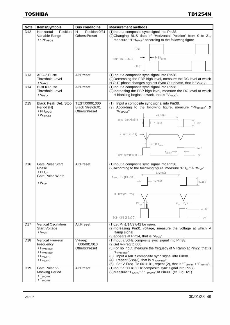
������� �����
Ver3.7 00/01/28 49
Note Items/Symbols Bus conditoins Measurement methodsD12 Horizontal Position
Variable Range / •PHHPOS
H Position:0/31Others:Preset
(1) Input a composite sync signal into Pin38.(2) Changing BUS data of “Horizontal Position” from 0 to 31,
measure "•PHHPOS" according to the following figure.
FBP in(Pin30)
(00)
(1F)
ĢPHHPOS
D13 AFC-2 PulseThreshold Level / VAFC2
All:Preset (1)Input a composite sync signal into Pin38.(2)Decreasing the FBP high level, measure the DC level at whichH OUT phase changes against Sync Out phase, that is "VAFC2".
D14 H-BLK PulseThreshold Level / VHBLK
All:Preset (1) Input a composite sync signal into Pin38.(2) Increasing the FBP high level, measure the DC level at which
H blanking begins to work, that is "VHBLK".
D15 Black Peak Det. StopPeriod (H) / PHBPDET
/ WBPDET
TEST:00001000Black Stretch:01Others:Preset
(1) Input a composite sync signal into Pin38.(2) According to the following figure, measure "PHBPDET" &
"WBPDET".
Sync in(Pin38)
H AFC(Pin29)
SCP OUT(Pin30)
63.5ƒÊs
4.7ƒÊs
ĢPHHPOS
WBPDET
4.3V
0V
0.25V
D16 Gate Pulse StartPhase / PHGP
Gate Pulse Width
/ WGP
All:Preset (1) Input a composite sync signal into Pin38.(2) According to the following figure, measure "PHGP" & "WGP".
Sync in(Pin38)
H AFC(Pin29)
SCP OUT(Pin30)
63.5ƒÊs
4.7ƒÊs
PHGP WGP
4.3V
0V
0.25V
D17 Vertical OscillationStart Voltage / VVON
All:Preset (1) Let Pin1/14/37/42 be open.(2) Increasing Pin31 voltage, measure the voltage at which V
Ramp signal(3) appears at Pin24, that is "VVON".
D18 Vertical Free-runFrequency / FVAUFR50
/ FVAUFR60
/ FV50FR
/ FV60FR
V-Freq: 000/001/010Others:Preset
(1) Input a 50Hz composite sync signal into Pin38.(2) Set V-Freq to 000.(3) For no input, measure the frequecy of V Ramp at Pin22, that is
"FVAUFR50".(3) Input a 60Hz composite sync signal into Pin38.(4) Repeat (2)&(3), that is “FVAUFR60”(5) Set V-Freq. To 001/101, repeat (2), that is "FV50FR" / "FV60FR".
D19 Gate Pulse V-Masking Period / T50GPM
/ T60GPM
All:Preset (1) Input a 50Hz/60Hz composite sync signal into Pin38.(2) Measure "T50GPM" / "T60GPM" at Pin30. (cf. Fig.D21)

������� �����
Ver3.7 00/01/28 50
Note Items/Symbols Bus conditoins Measurement methodsD20 V. Ramp DC on
Service Mode / VNOVRAMP
V STOP:1Others:Preset
(1) Set V STOP to 1.(2) Measure the DC level of Pin24, that is "VNOVRAMP".
D21 Vertical Pull-in Range(Auto) / FVPAUL
/ FVPAUH
Vertical Pull-in Range(50Hz) / FVP50L
/ FVP50H
Vertical Pull-in Range(60Hz) / FVP60L
/ FVP60H
V-Freq: 000/001/010Others:Preset
(6) Input a composite sync signal into Pin38.(7) For V-Freq 000/001/010, increasing the input vertical period
from 220H by 0.5H step, measure the period at which inputsignal synchronized with V Ramp(Pin24), that is "FVPAUL" /”FVP50L”/ "FVP60L".
(8) (3)For V-Freq 000/001/010, decreasing the input verticalperiod from 360H by 0.5H step, measure the period at whichinput signal synchronized with V Ramp, that is "FVPAUH" /”FVP50H”/ "FVP60H".
D22 Vertical Period onFixed Mode / TV3125
/ TV2625
/ TV313
/ TV263
V-Freq: 100/101/110/ 111 Others:Preset
For V-Freq 100/101/110/111, measure the vertical period at SCPout (Pin30), that is "TV312.5"/"TV262.5" / "TV313"/"TV263" .
D23 V-BLK Start Phase / PH50VBLK
/ PH60VBLK
V-BLK Width / W50VBLK
/ W60VBLK
All:Preset (1)Input a 50Hz/60Hz composite sync signal into Pin38.(2)Measure "T50AFCOFF" / "1T60AFCOFF" at Pin30. (cf. Fig.D25)
D24 Sand Castle PulseLevel / VSCPH
/ VSCPM
/ VSCPL
All:Preset Measure "VSCPH" / "VSCPM" / "VSCPL" at Pin30.
VSCPL
VSCPM
VSCPH
D25 Vertical RampAmplitude / VVRAMP
All:Preset Measure the V Ramp amplitude at Pin24, that is "VVRAMP".
D26 Vertical AMP Gain / GVAMP
Vertical AMPMax.Output Level / VVOMAX
Vertical AMPMin.Output Level
/ VVOMIN
All:Preset (1)Let Pin26 be open.(2)Changing the Pin25 DC voltage, measure "VVOMAX" / "VVOMIN" /"GVAMP" according to a following figure.
VVOMAX
VVOMIN
ĢV=GVAMP =20log(ĢV#26/ĢV#25)
#25DC
#26DC
D27 Vertical AMPMax.Output Current / IVOMAX
All:Preset (1)Supply 7V to Pin25.(2)Measure the current from Pin26 to GND, that is "IVOMAX".

������� �����
Ver3.7 00/01/28 51
Note Items/Symbols Bus conditoins Measurement methodsD28 Vertical NFB
Amplitude / VNFB
Vertical AmplitudeVariable Range / •VVRAMPH
/ •VVRAMPL
V Size:0/32/63Others:Preset
(1)Measure the amplitude of NFB V Ramp at Pin25, that is"VNFB". (2)Measure the amplitude of NFB V Ramp at Pin25 for V-Size 0/63, that is VNFBMIN / VNFBMAX.(3)Calculate; "•VVRAMPH"=(VNFBMAX-VNFB)/VNFB*100 "•VVRAMPL"=(VNFBMIN-VNFB)/VNFB*100
D29 Vertical LinearityVariable Range / •VLIN1+
/ •VLIN1-
/ •VLIN2+
/ •VLIN2-
V Linearity:0/8/15Others:Preset
(1)For V Linearity 8, measure V1(from center to max.) andV2(from center to min.) at Pin24 according to a follownig figure.(2)For V Linearity 15/0, measure VLIN1+ / VLIN1- and VLIN2+ / VLIN2-.(3)Calculate; "•VLIN1+"=(VLIN1+-V1)/V1*100 "•VLIN1-"=(VLIN1--V1)/V1*100 "•VLIN2+"=(VLIN2+-V2)/V2*100 "•VLIN2-"=(VLIN2--V2)/V2*100
V1
V2
Pin24signal
D30 Vertical S CorrectionVariable Range / •VS1+
/ •VS1-
/ •VS2+
/ •VS2-
V S Corr.:0/8/15Others:Preset
(1)For V S Correction:8, measure V1 and V2 at Pin24 according toa figure of NOTE:D32 .(2)For V S Correction:15/0, measure VS1+ / VS1- and VS2+ / VS2-.(3)Calculate; "•VS1+"=(VS1+-V1)/V1*100 "•VS1-"=(VS1--V1)/V1*100 "•VS2+"=(VS2+-V2)/V2*100 "•VS2-"=(VS2--V2)/V2*100
D35 Vertical GuardVoltage / VVG
All:Preset Decreasing the Pin25 voltage from 5V, measure the voltage atwhich Pin20 output drops to blanking level, that is "VVG".

������� �����
Ver3.7 00/01/28 52
+
CE202:1ƒÊF
TB12
54N
5650
5152
5354
5549
4344
4546
4748
4236
3738
3940
4135
2930
3132
3334
17
65
43
28
1413
1211
109
1521
2019
1817
1622
2827
2625
2423
SDA
SCL
Y/C GND
Ys/Ym SW
EXT.R IN
RGB Vcc(9V)
R OUT
G OUT
B OUT
APC Filter
X'tal
H Vcc(9V) V OUT
V NFB
IK IN
FBP IN/SCP OUT
H OUT
Dig. GND
Dig. VDD
DC Restor
H.AFC Filter ABCL IN
BLACK Det
Y/C Vcc(5V)
PIF tank
IF DET OUT
AFT OUT
C IN
SIF IN•^H CORRECTION IN
DE-EMP.
Sync IN
RIPPLE FIL
AUDIO OUT
IF AGC
IF GND
IF IN
IF IN
IF Vcc
LOOP Filter
NC
Y IN
DC NF
+
+
+
+
+
+
+
+
+
SA
W
Reg
.
+
+
+
+
+
+
+9V
+5V
+9V
87
65
43
21
910
1112
1314
1516
TC45
38B
P
8 76
54
32
1
910
1112
1314
TC74
HC
125P
N.C
.
N.C
.
SD
A
SC
L
H IN
FBP
TB12
54N
TE
ST
CIR
CU
IT
+
9 17 14 7 21
C2:
0.01
ƒÊF
R7:
430ƒ
C5:0.01ƒÊF
C6:0.01ƒÊF
CE8:2.2ƒÊF
R10:33kƒ¶ CE9:0.22ƒÊF
C7:2200pF
X1:4.433619MHz C8:9pF
C10:0.1ƒÊF
C11:0.1ƒÊF
C12:0.1ƒÊF
R14:75Ħ
R13:75Ħ
R12:75Ħ
C9:0.01ƒÊF
CE10:100ƒÊF
CE31:0.47ƒÊF
R39:100Ħ
R38:100Ħ
CE13:100ƒÊFC16:0.01ƒÊF
R52:4.7kĦ
R53:4.7kĦ
R50:51kĦ
CE24:10ƒÊF
R51:51kĦ
VR1:50kB
C30
:100
0pF
VR2:50kB
C29
:100
0pF
CE25:100ƒÊF
C31:0.01ƒÊF
CE26:47ƒÊF
C32:0.01ƒÊF
CE27:100ƒÊF
C019:0.01ƒÊF
R36:390ĦR37:
91Ħ
R20
6:27
0
CE19:0.22ƒÊF
CE21:1ƒÊF
R40:0pen
CE16:1ƒÊF
C23:0.1ƒÊF
C021:0.01ƒÊF
CE20:100ƒÊF
R42:3kĦR43:2kĦ
R41:470ƒ¶ CE22:0.22ƒÊF
C24:1000pF
CE23:10ƒÊF
CE3:22ƒÊF
C28:0.01ƒÊF
R49:1kĦ
R44
:33
0Ħ
L4:1
5ƒÊ
H
R46:1kĦ
R45:330Ħ
Q14
:
F1:Trap
L1:12ƒÊH
CE28:47ƒÊF
U IN
V IN
ref R
V RAMP
CW OUT
RF AGC
PIF tank
SIF OUT
EXT.G IN
EXT.B IN
R15:100Ħ
R16:3kĦ
+
+
C27:0.01ƒÊF
R47:51Ħ
C26:0.1ƒÊF
+
CE15:100ƒÊF
C18:0.01ƒÊF
R17:100Ħ
R19:100ĦR18:3kĦ
R20:3kĦ
+CE17:100ƒÊF
R21:100Ħ
+
R25
:1.
2kĦ
R27:510ĦR28:1.2kĦ
R24:100Ħ
R22:100Ħ
R23:10kĦ
CE11:100ƒÊF
R26:510Ħ
CE
4:10
0ƒÊ
F
CE18:1ƒÊF
C20:0.1ƒÊF
C22:0.1ƒÊF
+
C25:0.01ƒÊF
R48:1kĦ
Reg
.
+
+
+5V
+9VCE29:
47ƒÊF
CE30:100ƒÊF
C33:0.01ƒÊF
Reg.+ +
+5V +9V
CE
1:47
ƒÊF
CE
2:10
0ƒÊ
F
C1:
0.01
ƒÊF
+
CE7:4.7ƒÊF
R8:33kĦ
++
ZD1:4.7v
MON OUT
TV IN
EXT IN+CE201:1ƒÊF
R202:1kĦ
R201:1kĦ
R203:2kĦ
+CE203:4.7ƒÊF
EXT AUDIO
R205:680Ħ
R204:75Ħ
CE
5:
CE6:
C3:
C4
R1:
R2:R3:
R4:R5:
R6:
R11:
Q20
1
L2:
Q2:
Q1:
T1:
Q3:
Q4:
Q5:
Q6:
Q7:
Q8:
Q9:
SW2:
SW3:
P2
P3
Q15
:
SW
6:
T2:
F2:BPF
P1:
R300:10kĦ
75Ħ
75Ħ
C302:0.01ƒÊF
C13:8200pF
R32:1kĦ
R31:510Ħ
R30:1kƒ¶ C14:0.47ƒÊF
Q10:
R35:8.2kƒ¶CE14:0.22ƒÊF
C17:8200pF
+
R34:15kĦ
R29:5.6kĦ,1%
C106:2200pFR33:10kĦ
C15:0.1ƒÊF
D1:

������� �����
Ver3.7 00/01/28 53

������� �����
Ver3.7 00/01/28 54
+
CE202:1ƒÊF
TB12
54N
5650
5152
5354
5549
4344
4546
4748
4236
3738
3940
4135
2930
3132
3334
17
65
43
28
1413
1211
109
1521
2019
1817
1622
2827
2625
2423
SDA
SCL
Y/C GND
Ys/Ym SW
EXT.R IN
RGB Vcc(9V)
R OUT
G OUT
B OUT
APC Filter
X'tal
H Vcc(9V) V OUT
V NFB
IK IN
FBP IN/SCP OUT
H OUT
Dig. GND
Dig. VDD
DC Restor
H.AFC Filter ABCL IN
BLACK Det
Y/C Vcc(5V)
PIF tank
IF DET OUT
AFT OUT
C IN
SIF IN•^H CORRECTION IN
DE-EMP.
Sync IN
RIPPLE FIL
AUDIO OUT
IF AGC
IF GND
IF IN
IF IN
IF Vcc
LOOP Filter
NC
Y IN
DC NF
+
+
+
+
+
+
+
+
+
SA
W
Reg
.
+
+
+
+9V
+5V
+9V
TB12
54N
AP
PLI
CA
TIO
N C
IRC
UIT
+
C2:
0.01
ƒÊF
R7:
430ƒ
C5:0.01ƒÊF
C6:0.01ƒÊF
CE8:2.2ƒÊF
R10:33kƒ¶ CE9:0.22ƒÊF
C7:2200pF
X1:4.433619MHz C8:9pF
C10:0.1ƒÊF
C11:0.1ƒÊF
C12:0.1ƒÊF
R14:75Ħ
R13:75Ħ
R12:75Ħ
C9:0.01ƒÊF
CE10:100ƒÊF
CE31:0.47ƒÊF
R39:100Ħ
R38:100Ħ
100ƒÊF
0.01ƒÊF
CE26:47ƒÊF
C32:0.01ƒÊF
CE27:100ƒÊF
C019:0.01ƒÊF
R36:390ĦR37:
91Ħ
R20
6:27
0
CE19:0.22ƒÊF
CE21:1ƒÊF
R40:0pen
CE16:1ƒÊF
C23:0.1ƒÊF
C021:0.01ƒÊF
CE20:100ƒÊF
R42:3kĦR43:2kĦ
R41:470ƒ¶ CE22:0.22ƒÊF
C24:1000pF
CE23:10ƒÊF
CE3:22ƒÊF
C28:0.01ƒÊF
R49:1kĦ
R44
:33
0Ħ
L4:1
5ƒÊ
H
R46:1kĦ
R45:330Ħ
Q14
:
F1:Trap
L1:12ƒÊH
U IN
V IN
ref R
V RAMP
CW OUT
RF AGC
PIF tank
SIF OUT
EXT.G IN
EXT.B IN
R15:100Ħ
R16:3kĦ
+
+
C26:0.1ƒÊF
+
CE15:100ƒÊF
C18:0.01ƒÊF
R17:100Ħ
R19:100ĦR18:3kĦ
R20:3kĦ
+CE17:100ƒÊF
R21:100Ħ
CE
4:10
0ƒÊ
F
CE18:1ƒÊF
C20:0.1ƒÊF
C22:0.1ƒÊF
+
C25:0.01ƒÊF
R48:1kĦ
Reg.+
+5V +9V
CE
2:10
0ƒÊ
F
C1:
0.01
ƒÊF
+
CE7:4.7ƒÊF
R8:33kĦ
++
ZD1:4.7v
MON OUT
TV IN
EXT IN+CE201:1ƒÊF
R202:1kĦ
R201:1kĦ
R203:2kĦ
+CE203:4.7ƒÊF
EXT AUDIO
R205:680Ħ
R204:75Ħ
CE
5:
CE6:
C3:
C4
R1:
R2:R3:
R4:R5:
R6:
R11:
Q20
1
L2:
Q2:
Q1:
T1:
Q3:
P2
Q15
:
T2:
F2:BPF
P1:
R300:10kĦ
75Ħ
75Ħ
C302:0.01ƒÊF
C13:8200pF
R32:1kĦ
R31:510Ħ
R30:1kƒ¶ C14:0.47ƒÊF
Q10:
R35:8.2kƒ¶CE14:0.22ƒÊF
C17:8200pF
+
R34:15kĦ
R29:5.6kĦ,1%
C106:2200pFR33:10kĦ
C15:0.1ƒÊF
D1:
+
+9V
+
+9V
100ƒÊF
0.01ƒÊF
100ƒÊF
0.01ƒÊF

������� �����
Ver3.7 00/01/28 55
OUTLINE DRAWING Unit : mm
SDIP56-P-600-1.78

������� �����
Ver3.7 00/01/28 56
•••• ••• •••
p.1 IF stage for L system,AM sound demodulation ••
Chroma stage U/V input ports Cb/Cr input ports
P.2 Block Diagram Pin9 RFAGC/SIF in RF AGC
Ripple filter BIAS
L-SECAM AM ••
H.AFC •••••• ••••••
P.3 Pin3 SIF OUT Interface
3
5
14100Ħ
500Ħ15kĦ
9V
8.3kĦ
8.3kĦ
3
5
14100Ħ
500Ħ15kĦ
9V
16.3kĦ
16kĦ
Pin4 Audio out Interface
4
5
14
50kĦ
4.5V
ATT
9V
30kĦ
4
5
14
50kĦ
5.3V
ATT
9V
30kĦ
100Ħ
P.3 Pin6,7 IF IN 90dB• 90dB(• V)(Pin6-7)
field intensity level
P.4 Pin8 RF AGC/SIF IN RF AGC/SIF IN RF AGC
This terminal also lead to 1’st SIF
input pole.
••

������� �����
Ver3.7 00/01/28 57
8
5
145V
300Ħ
30kĦ
30kĦ
to SELF ADJ
5
1
500Ħ
10kĦ
9
5
149V
300Ħ
30kĦ
30kĦ
to SELF ADJ
P.4 Pin10 IF AGC 2.2mF 2.2• F
P.8 Pin36 Black DET
36
2.5V
19
42
4kĦ
36
2.5V
19
42
4kĦ
P.9 Pin40 DC restor
40
19
42
10k
50k
40
19
42
10k
50k
Pin38 Sync in 1401IRE 140IRE
p.10 Pin44,45 U/V in U/V in Cb/Cr in
P.11 Pin50,51 PIF tank 27pF 18pFp.14 RF AGC RF AGC delay point RF AGC delay point (Pin6-7)
01: 65dBm 01: 65 dB(•V)
3F: 100dBm 3F: 100 dB(• V)
P.15 DDS MODE SW•••
p.16 Split / Inter••• ••
p.17 U/V SW U/V Cb/Cr
p.18 Self Test 01:B OUT 10:R OUT ••
p.19 Self Adj. Self Adj. Self Test

������� �����
Ver3.7 00/01/28 58
00: AFT (Normal) 10: RF AGC X
1/2
Noise Det•
p.22 (*3)(*3)Pin 1, 4, 5, 11, 12, 19, 26, 33, 34,35, 42, 50, 51 are weak against •…
(*3)Pin 1, 4, 5, 6, 9, 11, 12, 13, 19, 26,31, 32, 33, 34, 35, 37, 42, 43, 50, 51are weak against •…
p.29 T4,T5 Cut off/Drive• spec.•• •••
T5 spec.••Drive• spec.••min. typ. max. 3 3.5 4-6.0 -5.5 -5.0
Drive• spec.••min. typ. max. 2.5 3.5 4.5 -8.0 -5.5 -4.5
T18 ••
p.35 S2 Input a signal that 4.5[MHz],
100[dB�V], 2.5[kHz]…•
Input a signal that 4.5[MHz],
100[dB�V], 25[kHz]…•
S3 Input a signal that 4.5[MHz],
100[dB�V], 2.5[kHz]…•
Input a signal that 4.5[MHz],
100[dB�V], 25[kHz]…•
p.36 S8 Input a signal that 4.5[MHz],
100[dB�V], 2.5[kHz]…•
Input a signal that 4.5[MHz],
100[dB�V], 25[kHz]…•
p.48 T18 ••
p.54 pin9 RF AGC/SIF IN RF AGC
Pin2 Ripple filter 10• F 22• F
p.55 Pin9 RF AGC/SIF IN RF AGC

This datasheet has been downloaded from:
www.DatasheetCatalog.com
Datasheets for electronic components.