Embed Size (px)
Citation preview

Altera Corporation AN-442-1.0
May 2007, version 1.0
Tool Flow for Design of DigitalIF for Wireless Systems
Application Note 442
Introduction This application note describes the tool flow that accelerates the hardware design of digital intermediate frequency (IF) systems comprising of digital up and down converters. The tool flow is based around the Altera® DSP Builder design entry tool, which provides high-level intellectual property (IP) megafunctions and control components that you may parameterize at a very low level. DSP Builder is intuitive to system designers that are familiar with the Simulink environment, but who are not necessarily familiar with hardware design and optimization techniques.
Using DSP Builder you can implement a fundamental wireless subsystem using minimal hardware resources. Furthermore, the time required to perform the design is significantly reduced with respect to the traditional methods. The tool flow breaks down the perceived barrier to entry associated with hardware design without compromising performance or productivity.
The tool flow has the following features:
■ Simple design entry of highly resource efficient digital IF chains ■ DSP Builder-based integration and validation to significantly reduce
the development time■ Parameterizable DSP IP to reduce development time and exploit
device features■ Architectural flexibility and simple integration using
parameterizable control components ■ Avalon® Streaming (Avalon-ST) interface strategy to reduce the
complexity of multiple channel designs
f For more information on the Avalon-ST interface, refer to the Avalon Streaming Interface Specification.
Digital IF Background
Digital IF processing provides the bridge between the baseband and analog RF portions of a wireless modem. A wireless system must convert between the low baseband sampling frequency and a high IF. Furthermore, a wireless system must mix the IF signal with a suitable carrier frequency.
6.1 1Preliminary

Tool Flow for Design of Digital IF for Wireless Systems
Typically, these conversions are achieved using a digital upconverter (DUC) to convert between baseband and IF and a digital downconverter (DDC) to convert between IF and baseband. These systems are implemented interpolators and decimators and low pass filters that remove undesirable spectral imaging and protect against aliasing. Figures 1 and 2 summarize these concepts.
Figure 1. DUC Schematic
Figure 2. DDC Schematic
Implementation Challenges
The future trends in wireless basestation specifications are tending towards multiple antennas, multiple carriers, and complex multiple input multiple output (MIMO) techniques, so you must implement digital IF modules that may process many different channels. Altera FPGAs are the ideal silicon platforms for this type of design, because you can exploit the high-speed dedicated multiplier units and parallel nature of hardware. In addition, the maximum frequency of operation of
I
Q
ChannelFilter
ChannelFilter
Interpolation
∑
Interpolation
NumericallyControlledOscillator
I
Q
Channel Filter
Channel Filter
Decimation
Decimation
NumericallyControlledOscillator
2 6.1 Altera CorporationPreliminary
Altera Solutions
modern FPGA devices is very much greater than the sampling frequency of the system, so you can time share the same hardware resources to process multiple channels. This time sharing reduces the overall cost of implementation.
Until now, design of systems that process multiple channels in a time shared fashion is a challenge, because each of the subsystems must support multiple channel processing and it must be possible to integrate them together easily. So you must synchronize the channelization of each individual hardware subsystem. Hand coded solutions are not very flexible given the volatility of new and future wireless standards and this is a significant disadvantage when it comes to changing the system level design and rearchitecting the system. Furthermore, implementation and verification of control logic that applies an appropriate schedule to the hardware resources is a significant overhead.
Digital IF modules are fundamental to a wireless modem, but unfortunately these modules are not differentiators in the marketplace and so it is desirable to reduce the development cost and time. The proposed tool flow significantly reduces the design time using a system level integration tool and provides the low level flexibility and hardware efficiency that is traditionally only achieved by hand-coded hardware description language.
Altera Solutions For the design of digital IF modems, the Altera DSP Builder offers a high level design entry point, which allows you to explore the design space, integrate IP and validate the system design.
Altera also supplies a portfolio of DSP IP, which is optimized for Altera FPGA devices. You can perform common DSP functions in a highly efficient manner and they are flexible and parameterizable at a low level. Using these modules saves time and money and reduces the verification overhead.
To simplify the integration of IP and other custom modules, Altera provides parameterizable control logic, which maximizes the design efficiency by increasing the level of time division multiplexing and multiple channelization.
Figure 3 summarizes the tool flow.
Altera Corporation 6.1 3Preliminary

Tool Flow for Design of Digital IF for Wireless Systems
Figure 3. Altera Digital IF Modem Tool Flow
Avalon-ST Interface
All DSP MegaCore® functions in the Altera IP portfolio have well defined interfaces that are compliant with the Avalon Streaming Interface Specification. You can exploit multiple Altera MegaCore functions and maximize productivity because the effort required to integrate them is trivial. In addition, it also facilitates interoperability between other third party IP and future releases from Altera. This section summarizes some of the key features of the Avalon-ST interface.
f For more information on the Avalon-ST interface, refer to the Avalon Streaming Interface Specification.
At the most fundamental level, the specification defines how to convey data between a source interface and a sink interface. Signaling of the integrity of the data is achieved by using a feed forward signal, valid. In addition, it defines how MegaCore functions may stall other blocks (backpressure) or regulate the rate at which data is provided and this is achieved using a feedback sideband signal, ready.
For the ready_latency = 0 mode, the following interaction occurs between the source interface (valid) and the sink interface (ready). Avalon-ST ready_latency is the number of cycles that a source must wait after a sink has asserted ready so that a data transfer is possible. The source interface provides valid data at the earliest time that it can, and it holds that piece of data until ready is asserted by the sink. The ready signal notifies the source interface that the piece of data has been sampled on that clock cycle. Figure 4 gives an example of the ready_latency = 0 behavior. On cycle one, the source provides data and asserts valid even though the sink is not ready. The source waits until cycle two and the sink acknowledges that it has sampled the data by asserting ready. On cycle
FIRCompiler
NCOCompiler
CICMegaCoreFunction
Packet Format Converter
Avalon Streaming Interface
DSP Builder
4 6.1 Altera CorporationPreliminary

Altera Solutions
three, the source happens to provide data on the same cycle that the sink is ready to receive it and so the transfer occurs immediately. On the fourth cycle, the sink is ready but because the source has not provided any valid data, the data bus is not sampled.
For the design of digital IF systems, Altera recommends ready_latency of 0 interfaces.
Figure 4. Ready Latency = 0 Behavior
A beat is defined as the transfer of one unit of data between a source and sink interface. This unit of data may consist of one or more symbols, so it can support modules that convey more than one piece of information on each valid cycle. In the context of wireless systems, this can be useful when conveying an in-phase and quadrature component on the same clock cycle. This concept is useful for a system designer because sometimes modules will have parallel input interfaces and other instances will require serial input interfaces. The choice depends on the algorithm, optimization technique and throughput requirements. Figure 5 gives an example of a data transfer where two symbols are conveyed on each beat - an In phase symbol I and a quadrature symbol Q. In this example, each symbol is eight bits wide.
clk
ready
valid
0 1 2 3 4 5 6 7 8
data D0 D1 D2 D3
Altera Corporation 6.1 5Preliminary

Tool Flow for Design of Digital IF for Wireless Systems
Figure 5. Packetized Data Transfer
The specification also describes several mechanisms to support the transfer of data associated with multiple channels. Altera recommend for Digital IF systems that this is achieved using packet based transfers where each packet has a deterministic format and each channel is allocated a specific field (time slot within a packet). Packet transfers require two additional signals that mark the start and the end of the packet. MegaCore functions may be designed with internal counters that count the samples in a packet so they know which channel a particular sample is associated with and in addition the MegaCore function should synchronize appropriately with the start and end of packet signals. Figure 5 gives an example where the in phase and quadrature components associated with three different channels are conveyed between two MegaCore functions.
Backpressure for Digital IF Systems
The inputs and outputs of a digital IF system are connected directly to an ADC/DAC—the system runs in a streaming fashion where the arrival of data is deterministic. Data is always available at a certain sampling frequency and so the IP should be parameterized to accept or generate data at the maximum rate required for the system. The Avalon-ST interface enables automatic channel synchronization and integration of different hardware algorithms while abstracting the required control complexity from the designer.
clk
ready
valid
0 1 2 3 4 5 6 7 8
data I 00
9 10
startofpacket
endofpacket
[15:8]
[7:0] Q 00
I 01
Q 01
I 02
Q 02
I 10
Q 10
I 11
Q 11
I 12
Q 12
6 6.1 Altera CorporationPreliminary
Altera Solutions
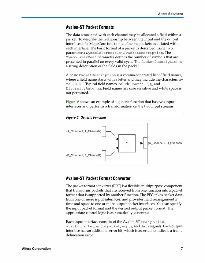
Avalon-ST Packet Formats
The data associated with each channel may be allocated a field within a packet. To describe the relationship between the input and the output interfaces of a MegaCore function, define the packets associated with each interface. The basic format of a packet is described using two parameters: SymbolsPerBeat, and PacketDescription. The SymbolsPerBeat parameter defines the number of symbols that are presented in parallel on every valid cycle. The PacketDescription is a string description of the fields in the packet.
A basic PacketDescription is a comma-separated list of field names, where a field name starts with a letter and may include the characters a-zA-Z0-9_. Typical field names include Channel1, Q, and DiversityAntenna. Field names are case sensitive and white space is not permitted.
Figure 6 shows an example of a generic function that has two input interfaces and performs a transformation on the two input streams.
Figure 6. Generic Function
Avalon-ST Packet Format Converter
The packet format converter (PFC) is a flexible, multipurpose component that transforms packets that are received from one function into a packet format that is supported by another function. The PFC takes packet data from one or more input interfaces, and provides field reassignment in time and space to one or more output packet interfaces. You can specify the input packet format and the desired output packet format. The appropriate control logic is automatically generated.
Each input interface consists of the Avalon-ST ready, valid, startofpacket, endofpacket, empty, and data signals. Each output interface has an additional error bit, which is asserted to indicate a frame delineation error.
(Q_Channel1, Q_Channel2)
(A_Channel1, A_Channel2)
?
(B_Channel1, B_Channel2)
Altera Corporation 6.1 7Preliminary

Tool Flow for Design of Digital IF for Wireless Systems
The PFC performs data mapping on a packet by packet basis, so that there is exactly one input packet on each input interface for each output packet on each output interface. The packet rate of the converter is limited by the interface with the longest packet. When the PFC has multiple output interfaces, the packets on each output interface are aligned so that the startofpacket signal is presented on the same clock cycle.
If each interface supports fixed-length packets, the multi-packet mapping option can be selected, and the PFC can map fields from multiple input packets to multiple output packets.
Examples
This section outlines some of the common operations that may be achieved using the PFC in a digital IF modem.
1 This section does not represent the full subset of operations that may be performed using this component.
Multiplex/Demultiplex
Often, you must time multiplex the data associated with multiple sources onto a single bus. For instance, the sampling frequency of the data captured from various antenna sources may have a sampling frequency that is significantly less than the clock frequency of the FPGA design. By multiplexing the data onto a single bus, you can exploit IP that is optimized to process time multiplexed input streams. Figure 7 gives an example if this configuration.
Figure 7. PFC Multiplexer Configuration
Antenna1
IP
Antenna2
Antenna3
Antenna4
Sink InterfaceFormat: (A1,A2,A3,A4)Symbols per beat: 4
Source InterfaceFormat: (A1,A2,A3,A4)Symbols per beat: 1
IP CoreSupports 4 channelsSink format: (A,B,C,D)Sink symbols per beat: 4
8 6.1 Altera CorporationPreliminary

Altera Solutions
Similarly, often after exploiting time division multiplexing within a design, demultiplex the channelized data stream so that the data may be passed off the chip or to other modules that do not support multiple channel processing. Figure 8 gives an example of a PFC demultiplexer configuration.
Figure 8. PFC Demultiplexer Configuration
Time Slot Rearrangement
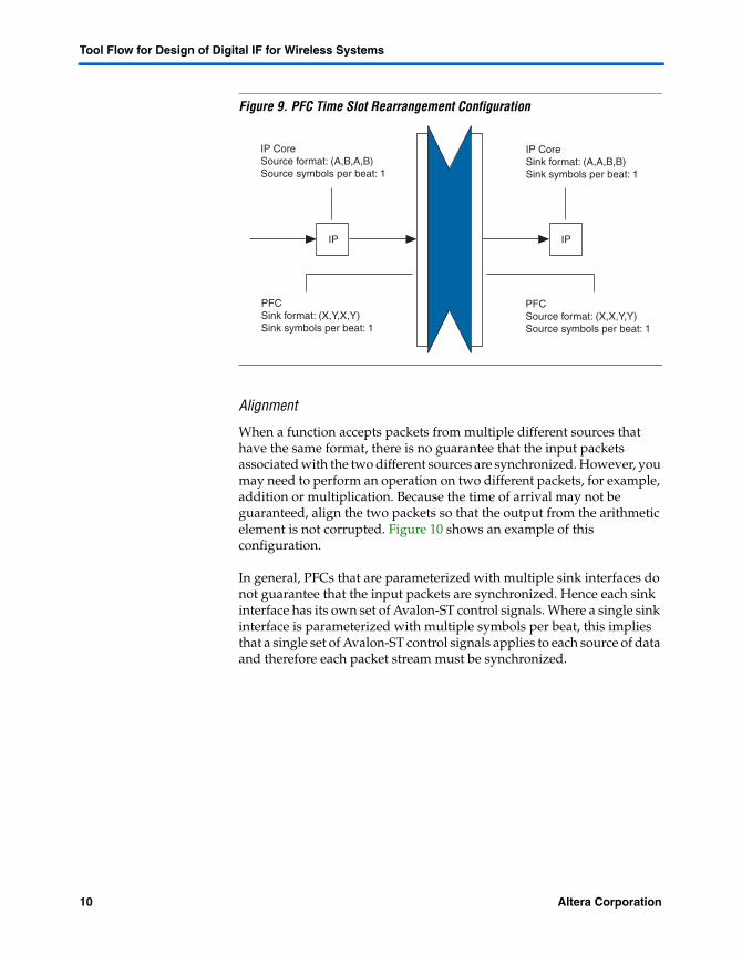
Sometimes you must reorder the samples within a packet. This scenario often arises when an algorithm is implemented in hardware to exploit certain optimizations, but the output may not be compatible with other IP. These incompatibilities may be bridged by the PFC, and this implementation strategy removes the effort required to verify custom time slot rearrangement logic. Figure 9 gives an example of a PFC time slot rearrangement configuration.
Antenna1
IP
Antenna2
Antenna3
Antenna4
Source InterfaceFormat: (A1,A2,A3,A4)Symbols per beat: 4
Sink InterfaceFormat: (A1,A2,A3,A4)Symbols per beat: 1
IP CoreSupports 4 channelsSource format: (IQ1,IQ2,IQ3,IQ4)Source symbols per beat: 1
Altera Corporation 6.1 9Preliminary
Tool Flow for Design of Digital IF for Wireless Systems
Figure 9. PFC Time Slot Rearrangement Configuration
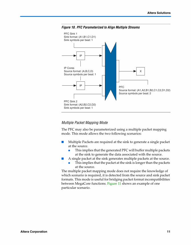
Alignment
When a function accepts packets from multiple different sources that have the same format, there is no guarantee that the input packets associated with the two different sources are synchronized. However, you may need to perform an operation on two different packets, for example, addition or multiplication. Because the time of arrival may not be guaranteed, align the two packets so that the output from the arithmetic element is not corrupted. Figure 10 shows an example of this configuration.
In general, PFCs that are parameterized with multiple sink interfaces do not guarantee that the input packets are synchronized. Hence each sink interface has its own set of Avalon-ST control signals. Where a single sink interface is parameterized with multiple symbols per beat, this implies that a single set of Avalon-ST control signals applies to each source of data and therefore each packet stream must be synchronized.
IP
PFCSource format: (X,X,Y,Y)Source symbols per beat: 1
IP CoreSource format: (A,B,A,B)Source symbols per beat: 1
IP
PFCSink format: (X,Y,X,Y)Sink symbols per beat: 1
IP CoreSink format: (A,A,B,B)Sink symbols per beat: 1
10 6.1 Altera CorporationPreliminary
Altera Solutions
Figure 10. PFC Parameterized to Align Multiple Streams
Multiple Packet Mapping Mode
The PFC may also be parameterized using a multiple packet mapping mode. This mode allows the two following scenarios:
■ Multiple Packets are required at the sink to generate a single packet at the source.● This implies that the generated PFC will buffer multiple packets
at the sink to generate the data associated with the source.■ A single packet at the sink generates multiple packets at the source.
● This implies that the packet at the sink is longer than the packets at the source.
The multiple packet mapping mode does not require the knowledge of which scenario is required, it is detected from the source and sink packet formats. This mode is useful for bridging packet format incompatibilities between MegaCore functions. Figure 11 shows an example of one particular scenario.
IP
PFCSource format: (A1,A2,B1,B2,C1,C2,D1,D2)Source symbols per beat: 2
X
PFC Sink 2Sink format: (A2,B2,C2,D2)Sink symbols per beat: 1
IP
IP CoresSource format: (A,B,C,D)Source symbols per beat: 1
PFC Sink 1Sink format: (A1,B1,C1,D1)Sink symbols per beat: 1
Altera Corporation 6.1 11Preliminary

Tool Flow for Design of Digital IF for Wireless Systems
Figure 11. PFC Parameterized in Multiple Packet Mapping Mode
For more information on the PFC and how to use it to simplify system level logic design using DSP Builder, see “Altera DSP Builder” on page 19.
DSP IP Portfolio
Altera MegaCore functions offer parameterizable hardware implementations of common DSP algorithms and the hardware is optimized for the Altera FPGA device families.
If you use MegaCore functions, the architectural flexibility allows you to explore a larger design space and at the same time reduce development cost because resources are not necessary for development of the DSP function and verification of the implementation.
You can parameterize all MegaCore functions using a consistent graphical user interface and the generated hardware has a well defined interface that makes it easy to integrate the MegaCore functions using the DSP Builder.
This section illustrates some of the features offered by the FIR Compiler, CIC MegaCore function and NCO Compiler.
IP
PFCSource format: (X,Y)Source symbols per beat: 1Multi Packet Mapping
IP CoreSource format: (A,A,B,B)Source symbols per beat: 1
IP
PFCSink format: (X,X,Y,Y)Sink symbols per beat: 1Multi Packet Mapping
IP CoreSink format: (A,B)Sink symbols per beat: 1
12 6.1 Altera CorporationPreliminary

Altera Solutions
FIR Compiler
The FIR Compiler MegaCore function implements hardware for single rate, interpolating, and decimating filters. You can use the coefficient generator to achieve the desired frequency response, or generate filter coefficients using a third party tool, for example, MATLAB and import using a text file.
The simplest description of a FIR filter is a tapped delay line. There are many different filter architectures that may be used to achieve this filter. Each trades off a combination of performance and throughput, logic area, dedicated multiplier utilization and memory usage. This reference design exploits the multi-cycle variable architecture with the aim to fit the DUC/DDC designs into the smallest device possible. Figure 12 shows the tapped delay line.
Figure 12. Tapped Delay Line
You must select the throughput required, with respect to the clock frequency chosen. The required throughput is a function of the data rate, the number of channels, and the clock rate. As a rule of thumb, the larger the number of clock cycles per input sample, the greater the degree of resource sharing within the filter. Furthermore by increasing the number of channels that the filter processes this increases the efficiency of the coefficient storage memory. The MegaCore function takes care of the complex scheduling required to achieve the most efficient hardware architecture. In addition, the interfaces support Avalon-ST interfaces and packetized data (for multiple channels) to reduce the effort of integration with other components.
xin
yout
Z -1 Z -1 Z -1 Z -1
C0 C1 C2 C3
TappedDelay Line
CoefficientMultipliers
Adder Tree
Altera Corporation 6.1 13Preliminary

Tool Flow for Design of Digital IF for Wireless Systems
Polyphase decomposition is exploited in interpolation and decimation filters to achieve a reduction in hardware resources because zero-stuffed data does not need to be computed when interpolating and the discarded data when decimating also does not require any filter computation.
Figure 13. FIR Compiler Parameterization Interface
CIC MegaCore Function
Cascaded integrator comb (CIC) filters are an economical class of DSP algorithm that may be used to efficiently implement a rate change. The key advantage to the use of CIC filters is that they do not require any multipliers to implement in hardware. In digital IF systems, they are typically exploited at the high sampling frequency stages where the amount of time sharing achievable is low and use of FIR filters leads to significant multiplier utilization. This strategy significantly reduces the total number of multipliers need to implement the processing chain.
A decimating CIC filter comprises a cascade of integrators, a decimator, and a cascade of differentiators. The response of the filter is determined by configuring the number of stages in each cascade (N), the rate change factor (R), and the number of delays in the differentiators (M). An interpolating CIC filter comprises of a cascade of differentiators, an interpolator, and a cascade of integrators.
14 6.1 Altera CorporationPreliminary

Altera Solutions
Figure 14. Integrator
Figure 15. Differentiator
Figure 16. Three Stage Decimating CIC
Figure 17. Three Stage Interpolating CIC
The main resource usage in a CIC filter is associated with the adders that exist in the each stage of the CIC filter. The size of these adders increases throughout the datapath due to the natural bit growth associated with the accumulators. Therefore, it is desirable to time share these adders to reduce the overall resource utilization. This time sharing is achieved by
1z
1zM
+
+
-
High Sampling Frequency Low Sampling Frequency
I I I R D D D�
Low Sampling Frequency High Sampling Frequency
I IRD D D
�
I
Altera Corporation 6.1 15Preliminary

Tool Flow for Design of Digital IF for Wireless Systems
modifying the architecture of the integrator and differentiators so that the length of the delay applied to the feedback (integrator) and feedforward (differentiator) paths is increased by a factor equal to the number of channels. In addition, the CIC MegaCore function also applies the powerful Hogenauer Pruning technique to further reduce the resource utilization.
f For more information, refer to the CIC MegaCore Function User Guide.
Often in a Digital IF design, there will be many channels that require filtering. Often it is not possible to time share only a single CIC filter because the integrator section with associated high sampling frequency will be fully used. However, because there is a rate change involved, the low rate differentiator section will not be fully used and simply instantiating multiple CIC filters will result in under used differentiator stages in each filter.
The CIC MegaCore function allows the flexibility to exploit time sharing of the low rate differentiator sections by providing multiple interfaces and processing chains for the high rate portions and combining all of the processing associated with the lower rate portions into a single processing chain. Note that the maximum number of interfaces is equal to the rate change factor. This strategy can lead to full utilization of the resources and this represents the most efficient hardware implementation. These architectures are known as Multiple Input Single Output for decimating filters, and Single Input Multiple output for interpolating filters.
Figure 18 shows an example of the MISO architecture for a CIC that processes a total of 4 channels. The sampling frequency of the input data allows you to time multiplex two channels per bus, so the CIC filter must be parameterized with two input interfaces. Because two interfaces are required, the rate change factor must also be at least two to exploit this architecture.
16 6.1 Altera CorporationPreliminary

Altera Solutions
Figure 18. Multiple Input Single Output Architecture
Figure 19 shows an example of the SIMO architecture for a CIC that processes a total of eight channels. The required sampling frequency of the output data allows you to time multiplex two channels per bus, so the CIC filter must be parameterized with four output interfaces. Because four interfaces are required, the rate change factor must also be at least four to exploit this architecture, but in this example a rate change of eight is demonstrated.
Figure 19. Single Input Multiple Output Architecture
Naturally the CIC MegaCore function supports the Avalon-ST interface, which allows you to input time multiplexed input signals into the MegaCore function.
Bus Utilization
100%
D D
2I I I �
D
2I I I �
(A,B,C,D)
(A,C)
(B,D)
50% 100%
Bus Utilization
50%
D D D
I I I8�
(A,E)
(A,B,C,D,E,F,G,H)
12.5% 100%
I I I8�
I I I8�
I I I8�
(B,F)
(C,G)
(D,H)
Altera Corporation 6.1 17Preliminary
Tool Flow for Design of Digital IF for Wireless Systems
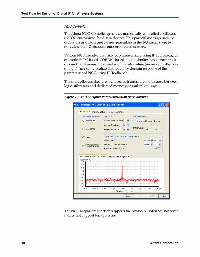
NCO Compiler
The Altera NCO Compiler generates numerically controlled oscillators (NCOs) customized for Altera devices. This particular design uses the oscillators as quadrature carrier generators in the I-Q mixer stage to modulate the I-Q channels onto orthogonal carriers.
Various NCO architectures may be parameterized using IP Toolbench, for example, ROM-based, CORDIC-based, and multiplier-based. Each trades of spur free dynamic range and resource utilization (memory, multipliers or logic). You can visualize the frequency domain response of the parameterized NCO using IP Toolbench.
The multiplier architecture is chosen as it offers a good balance between logic utilization and dedicated memory or multiplier usage.
Figure 20. NCO Compiler Parameterization User Interface
The NCO MegaCore function supports the Avalon-ST interface, however it does not support backpressure.
18 6.1 Altera CorporationPreliminary

Reference Designs
Altera DSP Builder
Altera DSP Builder is a design entry tool that provides a blockset for Mathworks Simulink and a method for targeting Altera FPGA from the Simulink description of the algorithm. You can prototype algorithmic designs, and when the functionality matches the desired behavior of the system you can generate the necessary HDL that is required to realize that system on an Altera FPGA.
You can parameterize the various building blocks with user interfaces. The functionality of the system is controlled with parameters. In addition to the DSP Builder blockset of components, you can use DSP Builder as an integration fabric of higher level MegaCore functions, which are parameterized using a GUI.
The Avalon-ST PFC is also available in the DSP Builder blockset and this may be used to easily parameterize a highly efficient datapath. The portfolio of configurable IP blocks and control logic leads to a very high design entry point, while enabling you to achieve a very low-level of architectural flexibility by modifying parameters.
In addition to providing you with a powerful integration fabric, the PFC may also be used to create hardware implementations of custom algorithms. For instance, you can use a PFC to condition the input data before performing some sort of transformation using components from the blockset. Two examples are a multiple channel average power calculator and an automatic gain control block.
Reference Designs
Altera provide reference designs to demonstrate the implementation of real digital IF systems for key wireless technologies, for example, wideband CDMA (W-CDMA) and WiMAX. This section outlines the system level design and hardware implementation of popular basestation configurations for W-CDMA.
f For more information on the WiMAX RF card system design, see AN 421: Accelerating WiMAX DUC & DDC System Designs.
Altera Corporation 6.1 19Preliminary

Tool Flow for Design of Digital IF for Wireless Systems
W-CDMA System Specifications and Design
The digital IF module must convert data between the chip rate fCHIP and the IF frequency fIF. Table 1 summarizes the sampling frequency specifications.
An IF frequency of 122.88 MHz allows digital predistortion (DPD) to be exploited in the transmitter, which relaxes the requirements of the power amplifier. At the receiver you can achieve increased performance in the rake receiver if the baseband sampling frequency is greater than the chip rate. The DDC downsamples the IF data down to twice the chip rate so that the paths may be searched with an accuracy of half a chip.
The configuration of the filters and the datapath are designed to minimize the required hardware resources and to achieve a W-CDMA compliant system. The resulting parameters are derived and summarized in this section, but the performance requirements that drive these specifications are given in “W-CDMA Specification Compliance” on page 31.
Multi-Stage Partitioning
To reduce the total required computational complexity, divide the sampling rate conversion into a cascade of stages. Figure 21 and Figure 22 show the multiple stage partitioning of the reference designs.
Table 1. Sampling Frequency Specifications
Parameter Specification
Baseband chip rate fCHIP 3.84 MHz
IF frequency fIF 122.88 MHz
Total sampling frequency change x32
20 6.1 Altera CorporationPreliminary

Reference Designs
Figure 21. DUC Schematic
Figure 22. DDC Schematic
For this application the rate change is decomposed into three stages where the lower rate stages (Filter G(z) and filter Q(z)) are implemented using finite impulse response filters and a CIC filter is used to perform the larger rate change (Filter P(z)).
Channel Filter Specification
The channel filter is designed to apply root raised cosine pulse shaping of the baseband data. To achieve a root raised cosine filter with 22% excess bandwidth, interpolate the baseband data by two. Figure 24 shows the resulting fixed point filter response.
■ Filter type: low pass root raised cosine■ Cut-off frequency: fCHIP/2■ Excess bandwidth: 22%■ Filter order: 40
Fs = 3.84 Msps
I
Q
NCO
Fs = 7.68 Msps Fs = 15.36 Msps Fs = 122.88 Msps
∑cos
sin
G(z)�
2Q(z)�
2P(z)�
8
G(z)�
2Q(z)�
2P(z)�
8
I
Q
NCO
Fs = 7.68 MspsFs = 15.36 MspsFs = 122.88 Msps
cos
sin
G(z)Q(z)
�2P(z)
�8
G(z)Q(z)
�2P(z)
�8
Altera Corporation 6.1 21Preliminary

Tool Flow for Design of Digital IF for Wireless Systems
Figure 23. Channel Filter Fixed Point Filter Response
CIC Compensation and Design
CIC filters have a low-pass filter characteristic. There are only three parameters that may be modified to achieve the desired passband characteristics and aliasing/imaging rejection. These parameters are the rate change factor R, the number of stages N, and the differential delay M.
For this application, the rate change factor is 8, and the input sampling frequency to the CIC filter is equal to four times the chip frequency. The output of the CIC filter is therefore sampled at thirty-two times the chip frequency.
To determine the other filter parameters, determine the relative bandwidth fc, which is calculated as the ratio of the desired cut-off frequency to the low sampling frequency. The following equation shows the relative bandwidth:
-10
-30
-20
-40
-50
-60
-70
-80
0
0 0.5 1.0 1.5 2.0 2.5 3.0 3.5
x106Frequency (MHz)
Mag
nitu
de (
dB)
fc0.5 fchip×4 fchip×
------------------------ 18---= =
22 6.1 Altera CorporationPreliminary
Reference Designs
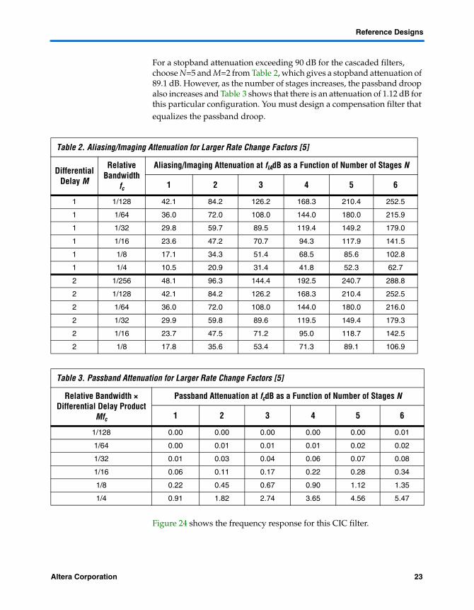
For a stopband attenuation exceeding 90 dB for the cascaded filters, choose N=5 and M=2 from Table 2, which gives a stopband attenuation of 89.1 dB. However, as the number of stages increases, the passband droop also increases and Table 3 shows that there is an attenuation of 1.12 dB for this particular configuration. You must design a compensation filter that equalizes the passband droop.
Figure 24 shows the frequency response for this CIC filter.
Table 2. Aliasing/Imaging Attenuation for Larger Rate Change Factors [5]
Differential Delay M
Relative Bandwidth
fc
Aliasing/Imaging Attenuation at fIAdB as a Function of Number of Stages N
1 2 3 4 5 6
1 1/128 42.1 84.2 126.2 168.3 210.4 252.5
1 1/64 36.0 72.0 108.0 144.0 180.0 215.9
1 1/32 29.8 59.7 89.5 119.4 149.2 179.0
1 1/16 23.6 47.2 70.7 94.3 117.9 141.5
1 1/8 17.1 34.3 51.4 68.5 85.6 102.8
1 1/4 10.5 20.9 31.4 41.8 52.3 62.7
2 1/256 48.1 96.3 144.4 192.5 240.7 288.8
2 1/128 42.1 84.2 126.2 168.3 210.4 252.5
2 1/64 36.0 72.0 108.0 144.0 180.0 216.0
2 1/32 29.9 59.8 89.6 119.5 149.4 179.3
2 1/16 23.7 47.5 71.2 95.0 118.7 142.5
2 1/8 17.8 35.6 53.4 71.3 89.1 106.9
Table 3. Passband Attenuation for Larger Rate Change Factors [5]
Relative Bandwidth × Differential Delay Product
Mfc
Passband Attenuation at fcdB as a Function of Number of Stages N
1 2 3 4 5 6
1/128 0.00 0.00 0.00 0.00 0.00 0.01
1/64 0.00 0.01 0.01 0.01 0.02 0.02
1/32 0.01 0.03 0.04 0.06 0.07 0.08
1/16 0.06 0.11 0.17 0.22 0.28 0.34
1/8 0.22 0.45 0.67 0.90 1.12 1.35
1/4 0.91 1.82 2.74 3.65 4.56 5.47
Altera Corporation 6.1 23Preliminary

Tool Flow for Design of Digital IF for Wireless Systems
Figure 24. CIC Frequency Response for R=8, M=2, N=5
To obtain the coefficients of a filter that equalizes the undesirable passband droop of the CIC is to construct an ideal frequency response and use the frequency sampling method to determine the coefficients. The ideal frequency response is determined by sampling the normalized magnitude response of the CIC filter before inverting the response. Generally, it is only necessary to equalize the response in the passband, but it is often recommended to sample further than the passband to tune the cascaded response of the filter chain.
An appropriate number of coefficients are chosen to provide satisfactory passband ripple and stopband attenuation. Figure 25 shows this process.
-20
-60
-40
-80
-100
-120
-140
0
0 1 2 3 4 5 6
x107Frequency (MHz)
Mag
nitu
de (
dB)
24 6.1 Altera CorporationPreliminary

Reference Designs
Figure 25. Compensation FIR Design Process
Figure 26 shows the resulting fixed point compensation response and specifications.
Figure 26. Compensation Filter Fixed Point Frequency Response
■ Filter type: low pass inverse sinc passband■ Filter order: 28
-10
-30
-20
-40
-50
-60
0
0 1 2 3 4 5 6 7
x106Frequency (MHz)
Mag
nitu
de (
dB)
Altera Corporation 6.1 25Preliminary

Tool Flow for Design of Digital IF for Wireless Systems
Datapath Specifications Summary
Table 4 shows a summary of the data path specifications to achieve the requirements of the W-CDMA specification.
Table 4. Data Path Specifications Summary
Parameter Specification DUC DDC
Channel filter G(z) Filter type FIR FIR
Taps 41 41
Rate change Interpolation 2 Single Rate
Coefficient bitwidth 18 18
Compensation Filter Q(z)
Filter type FIR FIR
Taps 29 29
Rate change Interpolation 2 Decimation 2
Coefficient bitwidth 18 18
CIC Filter P(z) Filter type CIC CIC
Number of stages 5 5
Differential delay 2 2
Rate change Interpolation 8 Decimation 8
NCO Spurious free dynamic range
100 dB 100 dB
Data Path Bit width 16 16
Rounding method Convergent Convergent
26 6.1 Altera CorporationPreliminary

Reference Designs
Figure 27. Cascaded Filter Chain Fixed Point Frequency Response
Efficient Hardware Implementation
A popular W-CDMA base station (BS, or BTS) configuration requires a digital IF circuit to perform Digital Up and Down conversion associated with two diversity antennas, four carriers and three sectors. To exploit the maximum efficiency in Stratix III devices, a clock frequency of 245.76 MHz is chosen, and the following architectures are used for the DUC and DDC. These architectures processes two diversity antennas, four carriers, and one sector, and so to scale the processing to support three sectors, duplicate the design three times.
-20
-60
-40
-80
-120
-140
-160
-200
0
0 1 2 3 4 5 6
x107Frequency (MHz)
Mag
nitu
de (
dB)
-100
-180
W-CDMA Frequency Response
Altera Corporation 6.1 27Preliminary

Tool Flow for Design of Digital IF for Wireless Systems
Figure 28. W-CDMA DUC (4 Carrier, 1 Sector, Diversity)
I 1
Q1
Q2
I 2
I 3
Q3
Q4
I 4
I 5
Q5
Q6
I 6
I 7
Q7
Q8
I 8
1
3
4
2
NCO
�8
�CIC
NCO
FIR
2�FIR
2
1
3
4
2
1
2
3
4
I 1 Q1
I 4 Q4
I 3 Q3
[ , ]
NCO
NCO [ , ]
I 2 Q2[ , ]
Fs =3.84 Msps
Fs = 61.44 Msps
Fs = 122.88 Msps
Fs = 122.88 Msps
Fs = 245.76 Msps
[ , ]
28 6.1 Altera CorporationPreliminary
Reference Designs
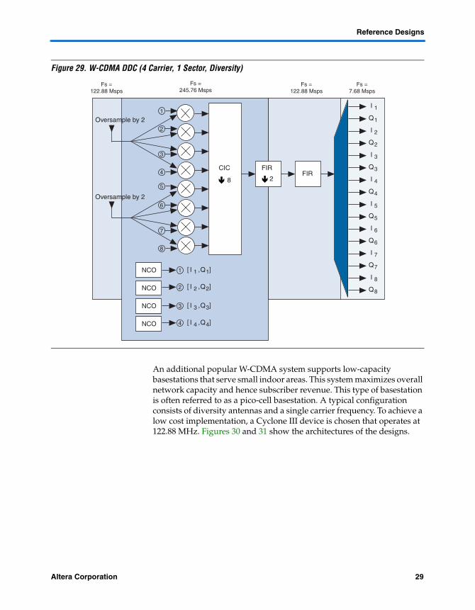
Figure 29. W-CDMA DDC (4 Carrier, 1 Sector, Diversity)
An additional popular W-CDMA system supports low-capacity basestations that serve small indoor areas. This system maximizes overall network capacity and hence subscriber revenue. This type of basestation is often referred to as a pico-cell basestation. A typical configuration consists of diversity antennas and a single carrier frequency. To achieve a low cost implementation, a Cyclone III device is chosen that operates at 122.88 MHz. Figures 30 and 31 show the architectures of the designs.
I 1
Q1
Q2
I 2
I 3
Q3
Q4
I 4
I 5
Q5
Q6
I 6
I 7
Q7
Q8
I 8
1
3
48�
CICFIR
2�
FIR
2
5
6
7
8
NCO
NCO
1
2
I 1 Q1[ , ]
I 2 Q2[ , ]
NCO
NCO
3
4
I 3 Q3[ , ]
I 4 Q4[ , ]
Fs =7.68 Msps
Fs =122.88 Msps
Fs =122.88 Msps
Fs =245.76 Msps
Oversample by 2
Oversample by 2
Altera Corporation 6.1 29Preliminary

Tool Flow for Design of Digital IF for Wireless Systems
Figure 30. W-CDMA Picocell DUC Architecture
Figure 31. W-CDMA Picocell DDC Architecture
Q
2�
2�
8�CIC
IQ
FIR FIR
I
Q
I
I 11Q 11I 21
Q 21
NCO
Fs =30.72 Msps
Fs = 61.44 Msps
Fs = 122.88 Msps
Fs = 15.36 Msps
Fs = 3.84 Msps
Q
2�8�
CIC
IQ
FIR FIR
I
Q
I
I 11Q 11I 21
Q 21
NCO
Fs =30.72 Msps
Fs = 61.44 Msps
Fs = 122.88 Msps
Fs = 7.68 Msps
30 6.1 Altera CorporationPreliminary
Reference Designs
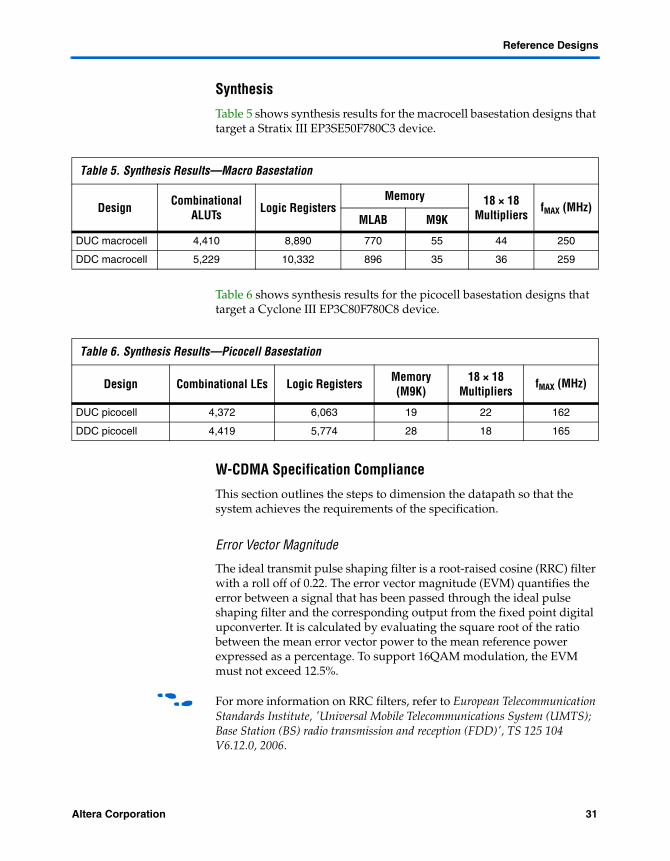
Synthesis
Table 5 shows synthesis results for the macrocell basestation designs that target a Stratix III EP3SE50F780C3 device.
Table 6 shows synthesis results for the picocell basestation designs that target a Cyclone III EP3C80F780C8 device.
W-CDMA Specification Compliance
This section outlines the steps to dimension the datapath so that the system achieves the requirements of the specification.
Error Vector Magnitude
The ideal transmit pulse shaping filter is a root-raised cosine (RRC) filter with a roll off of 0.22. The error vector magnitude (EVM) quantifies the error between a signal that has been passed through the ideal pulse shaping filter and the corresponding output from the fixed point digital upconverter. It is calculated by evaluating the square root of the ratio between the mean error vector power to the mean reference power expressed as a percentage. To support 16QAM modulation, the EVM must not exceed 12.5%.
f For more information on RRC filters, refer to European Telecommunication Standards Institute, 'Universal Mobile Telecommunications System (UMTS); Base Station (BS) radio transmission and reception (FDD)', TS 125 104 V6.12.0, 2006.
Table 5. Synthesis Results—Macro Basestation
Design Combinational ALUTs Logic Registers
Memory 18 × 18 Multipliers
fMAX (MHz)MLAB M9K
DUC macrocell 4,410 8,890 770 55 44 250
DDC macrocell 5,229 10,332 896 35 36 259
Table 6. Synthesis Results—Picocell Basestation
Design Combinational LEs Logic Registers Memory (M9K)
18 × 18 Multipliers
fMAX (MHz)
DUC picocell 4,372 6,063 19 22 162
DDC picocell 4,419 5,774 28 18 165
Altera Corporation 6.1 31Preliminary

Tool Flow for Design of Digital IF for Wireless Systems
The EVM achieved by the filter chain in this design is better than 2% and this measurement was acquired using the test harness, see Figure 32.
Figure 32. EVM Test Harness
Transmit Spectral Mask
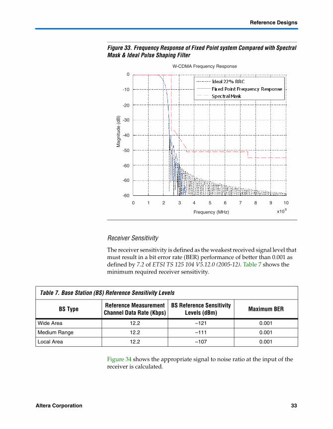
Equipment manufacturers are required to ensure their systems comply with the spectral regulations described by 6.6.2.1 of the ETSI TS 125 104 V5.12.0 (2005-12) specification. The filtering must therefore be designed so that there is no spectral radiation above the specified levels beyond the allowed channel bandwidth. This design helps to increase capacity and enables the coexistence of other telecommunication systems in adjacent frequency spectrum. Figure 33 shows the fixed point frequency response.
�
Fixed Point DUC
�
ReferenceDUC
CalculateEVM
16QAMSource
CodeGenerator
oo oooo oooo oooo oo
32 6.1 Altera CorporationPreliminary
Reference Designs
Figure 33. Frequency Response of Fixed Point system Compared with Spectral Mask & Ideal Pulse Shaping Filter
Receiver Sensitivity
The receiver sensitivity is defined as the weakest received signal level that must result in a bit error rate (BER) performance of better than 0.001 as defined by 7.2 of ETSI TS 125 104 V5.12.0 (2005-12). Table 7 shows the minimum required receiver sensitivity.
Figure 34 shows the appropriate signal to noise ratio at the input of the receiver is calculated.
-10
-30
-20
-40
-50
-60
0
0 1 2 3 4 5 6 7
x106Frequency (MHz)
Mag
nitu
de (
dB)
-60
-60
8 9 10
W-CDMA Frequency Response
Table 7. Base Station (BS) Reference Sensitivity Levels
BS Type Reference Measurement Channel Data Rate (Kbps)
BS Reference Sensitivity Levels (dBm) Maximum BER
Wide Area 12.2 –121 0.001
Medium Range 12.2 –111 0.001
Local Area 12.2 –107 0.001
Altera Corporation 6.1 33Preliminary

Tool Flow for Design of Digital IF for Wireless Systems
Figure 34. Signal to Noise Ratio Derivation
The following constants are assumed:
■ K: Boltzmann constant = 1.38 × 10⁻²³ m2.kg.s-2.K-1
■ T: temperature 290 K■ B: bandwidth 3.84 x 10⁶ Hz■ γ: spreading factor 16
Assuming the worst case sensitivity level (for a wide-area basestation) the following equation gives the signal to noise ratio at the antenna connector:
Receiver SNR (dB) = Receiver sensitivity (dB) – (noise floor (dB) – spread gain (dB))
= –151 –(–138 – 24)= 11
1 The receiver sensitivity is a function of the entire modem performance because there are several areas where distortion may occur. For instance, performance of the Synchronization, rake receiver and Turbo decoders directly affects the receiver sensitivity.
Figure 35 shows the receiver sensitivity test harness.
Receiver Sensitivity (dB) = Receiver Sensitivity (dBm) - 30
Receiver Signal to Noise Ratio (dB)
Noise Floor (dB) - Spread Gain (dB)
Spread Gain (dB) = 20log10(γ)
Noise Floor (dB) = 10log10 (kTB)
dB
34 6.1 Altera CorporationPreliminary
Reference Designs
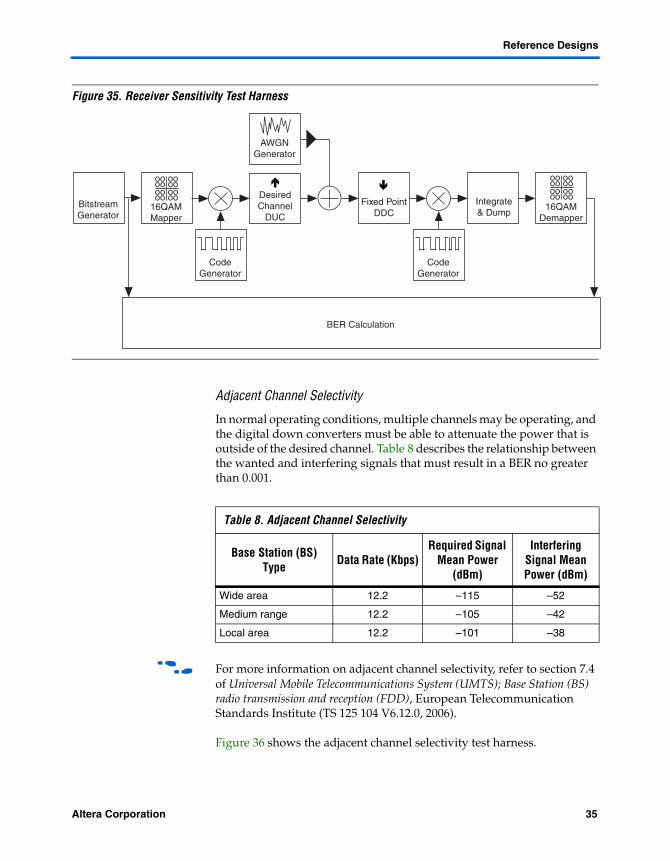
Figure 35. Receiver Sensitivity Test Harness
Adjacent Channel Selectivity
In normal operating conditions, multiple channels may be operating, and the digital down converters must be able to attenuate the power that is outside of the desired channel. Table 8 describes the relationship between the wanted and interfering signals that must result in a BER no greater than 0.001.
f For more information on adjacent channel selectivity, refer to section 7.4 of Universal Mobile Telecommunications System (UMTS); Base Station (BS) radio transmission and reception (FDD), European Telecommunication Standards Institute (TS 125 104 V6.12.0, 2006).
Figure 36 shows the adjacent channel selectivity test harness.
AWGNGenerator
�
DesiredChannel
DUC
BER Calculation
16QAMMapper
CodeGenerator
BitstreamGenerator
�Fixed Point
DDCIntegrate& Dump
CodeGenerator
16QAMDemapper
oo oooo oooo oooo oo
oo oooo oooo oooo oo
Table 8. Adjacent Channel Selectivity
Base Station (BS) Type Data Rate (Kbps)
Required Signal Mean Power
(dBm)
Interfering Signal Mean Power (dBm)
Wide area 12.2 –115 –52
Medium range 12.2 –105 –42
Local area 12.2 –101 –38
Altera Corporation 6.1 35Preliminary

Tool Flow for Design of Digital IF for Wireless Systems
Figure 36. Adjacent Channel Selectivity Test Harness
Getting Started This section describes the following topics:
■ System Requirements■ Install the Reference Design■ W-CDMA Design Walkthrough
System Requirements
The reference design requires the following hardware and software.
■ MATLAB version R2006B■ Simulink version R2006B■ Quartus® II software version 7.1■ DSP Builder version 7.1■ FIR Compiler version 7.1■ CIC MegaCore function version 7.1■ NCO Compiler version 7.1
The following software is optional:
■ MATLAB Signal Processing Toolbox■ MATLAB Signal Processing Blockset
AdjacentChannelInterferer
�
DesiredChannel
DUC
BER Calculation
16QAMMapper
CodeGenerator
BitstreamGenerator
�Fixed Point
DDCIntegrate& Dump
CodeGenerator
16QAMDemapper
oo oooo oooo oooo oo
oo oooo oooo oooo oo
36 6.1 Altera CorporationPreliminary

Getting Started
Install the Reference Design
To install the reference design, run the an442-v7.1.exe file and follow the installation instructions.
The reference design is installed by default in the directory c:\altera\reference_designs\if_modem\71. You can change the default directory during the installation.
Figure 37 shows the directory structure after installation.
Figure 37. Reference Design Directory Structure
To use the reference designs and use the Altera digital IF modem custom library, add the custom library to the MATLAB path, by following these steps:
1. Launch MATLAB.
2. On the File Menu, select Set Path.
3. Add <installation directory>\library to the path.
4. Save the path.
5. To prepare each design for simulation, open the design, and then type alt_dspbuilder_refresh_megacore from the MATLAB command line. This function generates a simulation model for each of the MegaCore functions in the design.
ddc_multichannelContains the 4 carrier, 1 sector, diversity DDC design.
ddc_picoContains the picocell DDC design
duc_picoContains the picocell DUC design
duc_multichannelContains the 4 carrier, 1 sector, diversity DUC design.
docContains all documentation for the IF modem.
libraryContains the library components for the rounding and mixer.
tutorialContains a skeleton design for tutorial purposes.
<path>Installation directory.
wcdmaContains the W-CDMA files.
Altera Corporation 6.1 37Preliminary

Tool Flow for Design of Digital IF for Wireless Systems
W-CDMA Design Walkthrough
This design walkthrough implements a W-CDMA DDC that is suitable for a picocell basestation. It supports a single carrier, one sector, and two diversity antennas. It requires a clock frequency of 122.88 MHz, and so is therefore suitable for targeting the Cyclone III device family.
1. To create the design, load the skeleton design (ddc_pico.mdl) from the <installation directory>\tutorial directory. To examine the completed design, load the ddc_pico.mdl from the <installation directory>\wcdma\ddc_pico\ directory. Figure 38 shows the design architecture.
Figure 38. W-CDMA Picocell DDC Tutorial Architecture
2. The skeleton model file contains the top level hierarchy and the ports associated with the design.
3. Double click on the ddc_nco subsystem, and then click on the Simulink Library Browser and browse to Altera DSP builder, MegaCore functions.
4. Drag an instance of the NCO MegaCore function into the subsystem, and double click to parameterize.
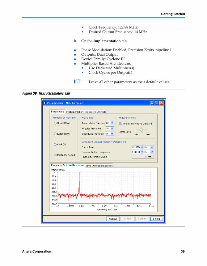
5. Parameterize the NCO using the following parameters (see Figures 39 and 40):
a. On the Parameters tab:
● Generation Algorithm: Multiplier Based● Precision: Accumulator 22bits, Angular 16bits, Magnitude
16bits● Generated Output Clock Frequency Parameters:
I 11
Q11
I 21
Q21
8�
CICFIR
2�
FIR
NCO
Fs=7.68 MspsFs=30.72 MspsFs=122.88 Msps
DDC
DDC
I
Q
I
Q
I
Q
Fs=61.44 Msps
38 6.1 Altera CorporationPreliminary
Getting Started
• Clock Frequency: 122.88 MHz• Desired Output Frequency: 14 MHz
b. On the Implementation tab:
● Phase Modulation: Enabled, Precision 22bits, pipeline 1● Outputs: Dual Output● Device Family: Cyclone III● Multiplier Based Architecture:
• Use Dedicated Multiplier(s)• Clock Cycles per Output: 1
1 Leave all other parameters as their default values.
Figure 39. NCO Parameters Tab
Altera Corporation 6.1 39Preliminary

Tool Flow for Design of Digital IF for Wireless Systems
Figure 40. NCO Implementation Tab
6. When you have parameterizing the NCO MegaCore function, click Finish, then Generate.
7. Connect all signals as appropriate.
8. Return to the top-level design of the hierarchy and navigate to the Altera IF Modem Library in the Simulink Library browser.
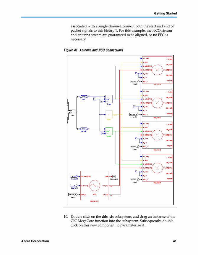
9. Drag four of the mixer components into the design from the data path sub library and connect up the antennas and the NCO (see Figure 41). Given the sampling frequency of the NCO carrier and the data from the antenna, data is valid on every clock cycle and therefore this must be driven by a binary 1. As each data bus is only
40 6.1 Altera CorporationPreliminary
Getting Started
associated with a single channel, connect both the start and end of packet signals to this binary 1. For this example, the NCO stream and antenna stream are guaranteed to be aligned, so no PFC is necessary.
Figure 41. Antenna and NCO Connections
10. Double click on the ddc_cic subsystem, and drag an instance of the CIC MegaCore function into the subsystem. Subsequently, double click on this new component to parameterize it.
Altera Corporation 6.1 41Preliminary

Tool Flow for Design of Digital IF for Wireless Systems
11. Parameterize the CIC using the following parameters (see Figures 42 and 43):
a. On the Architecture tab:
● Device Family: Cyclone III● Filter Specifications:
• Filter Type: decimator• Number of Stages: 5• Differential Delay: 2• Rate Change Factor: 8
● Multichannel options:• Number of interfaces: 8• Number of channels per interface: 2
● Data Storage Options• Differentiator Data Storage: Memory
b. On the Input/Output Options tab
● Input Options• Input Data Width: 16bits
● Output Options• Output Data width: 16bits• Output Rounding Options: convergent Rounding• Apply Hogenauer Pruning across filter stages: enabled
42 6.1 Altera CorporationPreliminary

Getting Started
Figure 42. CIC Architecture Tab
Altera Corporation 6.1 43Preliminary

Tool Flow for Design of Digital IF for Wireless Systems
Figure 43. CIC Input/Output Options Tab
12. When you have parameterizing the CIC MegaCore function, click Finish, then Generate.
13. Connect up all of the signals as appropriate
14. Return to the top level of the hierarchy and double click on the ddc_fir_compensation subsystem
44 6.1 Altera CorporationPreliminary

Getting Started
15. Parameterize the FIR filter using the following parameters and click Generate. From the coefficients tab, import the ddc_fir_compcoef.txt file.
16. Navigate to the Altera Digital IF modem library, and instance a rounding block at the output of the filter. Double click on the block to ensure that the data widths are correct. Connect all of the signals in the subsystem together to their appropriate ports.
17. Return to the top level of the hierarchy and double click on the ddc_fir_channel subsystem
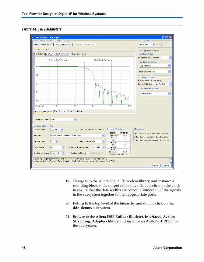
18. Parameterize the FIR filter using the following parameters (see Figure 44) and click Generate. From the coefficients tab, import the ddc_fir_channel.txt file.
Altera Corporation 6.1 45Preliminary
Tool Flow for Design of Digital IF for Wireless Systems
Figure 44. FIR Parameters
19. Navigate to the Altera Digital IF modem library, and instance a rounding block at the output of the filter. Double click on the block to ensure that the data widths are correct. Connect all of the signals in the subsystem together to their appropriate ports.
20. Return to the top level of the hierarchy and double click on the ddc_demux subsystem.
21. Browse to the Altera DSP Builder Blockset, Interfaces, Avalon Streaming, Adapters library and instance an Avalon-ST PFC into the subsystem.
46 6.1 Altera CorporationPreliminary

Getting Started
22. Double click on the PFC, and select the following parameters (see Figures 45 through 40):
● Number of sinks: 1● Number of sources: 1● Symbol Width: 16● Sink Format 1: 'I1,Q1,I2,Q2'● Sink 1 Symbols per Beat: 1● Source Format 1: 'I1,Q1,I2,Q2'● Source 1 Symbols per Beat: 4
Figure 45. PFC Parameters—General
Altera Corporation 6.1 47Preliminary

Tool Flow for Design of Digital IF for Wireless Systems
Figure 46. PFC Parameters—Sink Format
Figure 47. PFC Parameters—Sink Sym/Beat
48 6.1 Altera CorporationPreliminary

Getting Started
Figure 48. PFC Parameters—Source Format
Figure 49. PFC Parameters—Source Sym/Beat
23. Connect up all signals as appropriate. Then, return to the top-level design and double click on Signal Compiler to synthesize the design.
Figure 50 shows the complete design.
Altera Corporation 6.1 49Preliminary

Tool Flow for Design of Digital IF for Wireless Systems
Figure 50. Complete Design
Conclusion This application note described the design of digital IF systems using Altera tools. It consists of a high-level design entry point using DSP Builder to parameterize a digital IF data path consisting of highly parameterizable IP and flexible control logic components. The IP exploits hardware design techniques, so you can achieve a design that uses the minimum device resources while at the same time significantly reduces design time.
50 6.1 Altera CorporationPreliminary
101 Innovation DriveSan Jose, CA 95134www.altera.comLiterature Services:[email protected]
Copyright © 2007 Altera Corporation. All rights reserved. Altera, The Programmable Solutions Company,the stylized Altera logo, specific device designations, and all other words and logos that are identified astrademarks and/or service marks are, unless noted otherwise, the trademarks and service marks of AlteraCorporation in the U.S. and other countries. All other product or service names are the property of their re-spective holders. Altera products are protected under numerous U.S. and foreign patents and pendingapplications, maskwork rights, and copyrights. Altera warrants performance of its semiconductor productsto current specifications in accordance with Altera's standard warranty, but reserves the right to make chang-es to any products and services at any time without notice. Altera assumes no responsibility or liabilityarising out of the application or use of any information, product, or service describedherein except as expressly agreed to in writing by Altera Corporation. Altera customersare advised to obtain the latest version of device specifications before relying on any pub-lished information and before placing orders for products or services.