Embed Size (px)
Citation preview

7/31/2019 Xilinx-hdl Tool Flow
http://slidepdf.com/reader/full/xilinx-hdl-tool-flow 1/37
1
HDL (Hardware Description
Language) – XILINX TOOL FLOW
By
SUNIL MP

7/31/2019 Xilinx-hdl Tool Flow
http://slidepdf.com/reader/full/xilinx-hdl-tool-flow 2/37
2
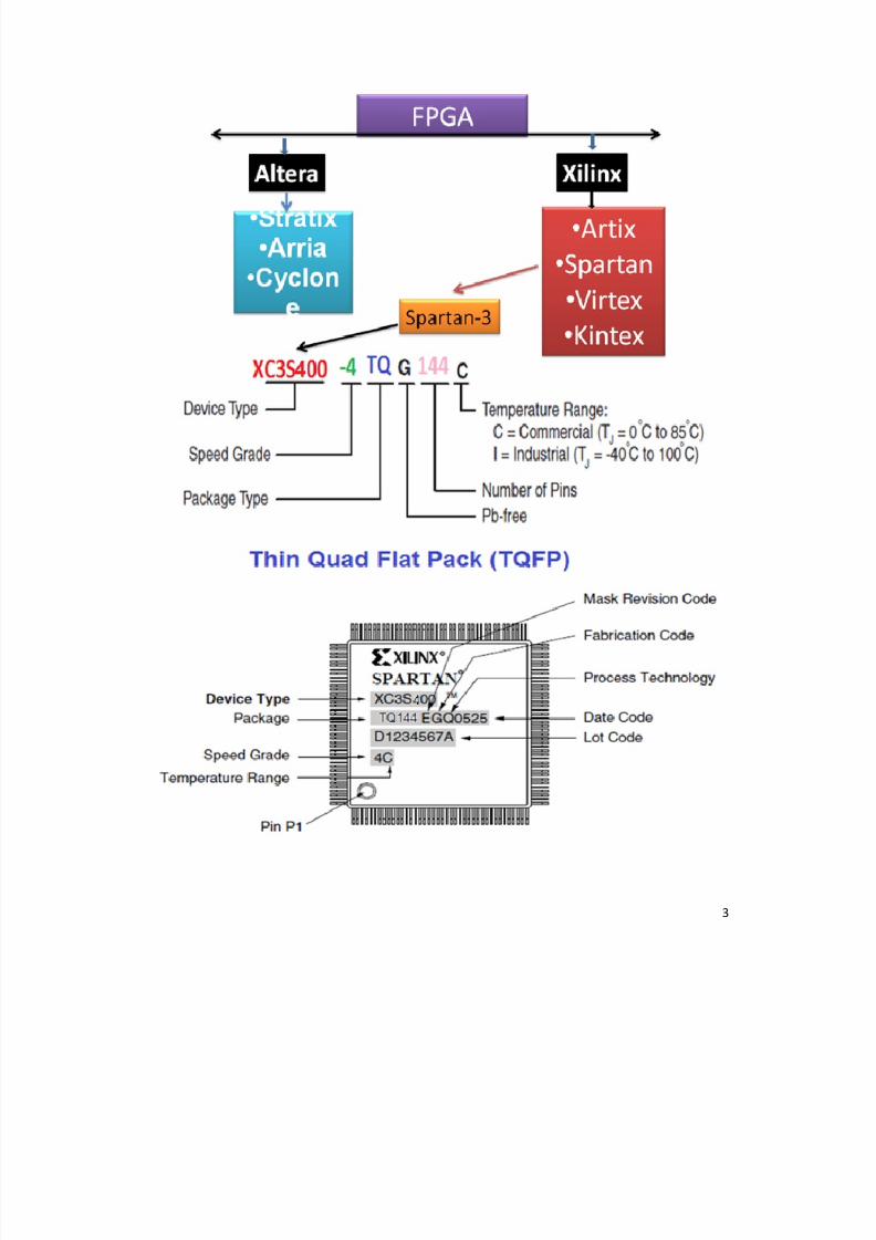
SPARTAN -3 FPGA IC
7/31/2019 Xilinx-hdl Tool Flow
http://slidepdf.com/reader/full/xilinx-hdl-tool-flow 3/37
3
7/31/2019 Xilinx-hdl Tool Flow
http://slidepdf.com/reader/full/xilinx-hdl-tool-flow 4/37
4
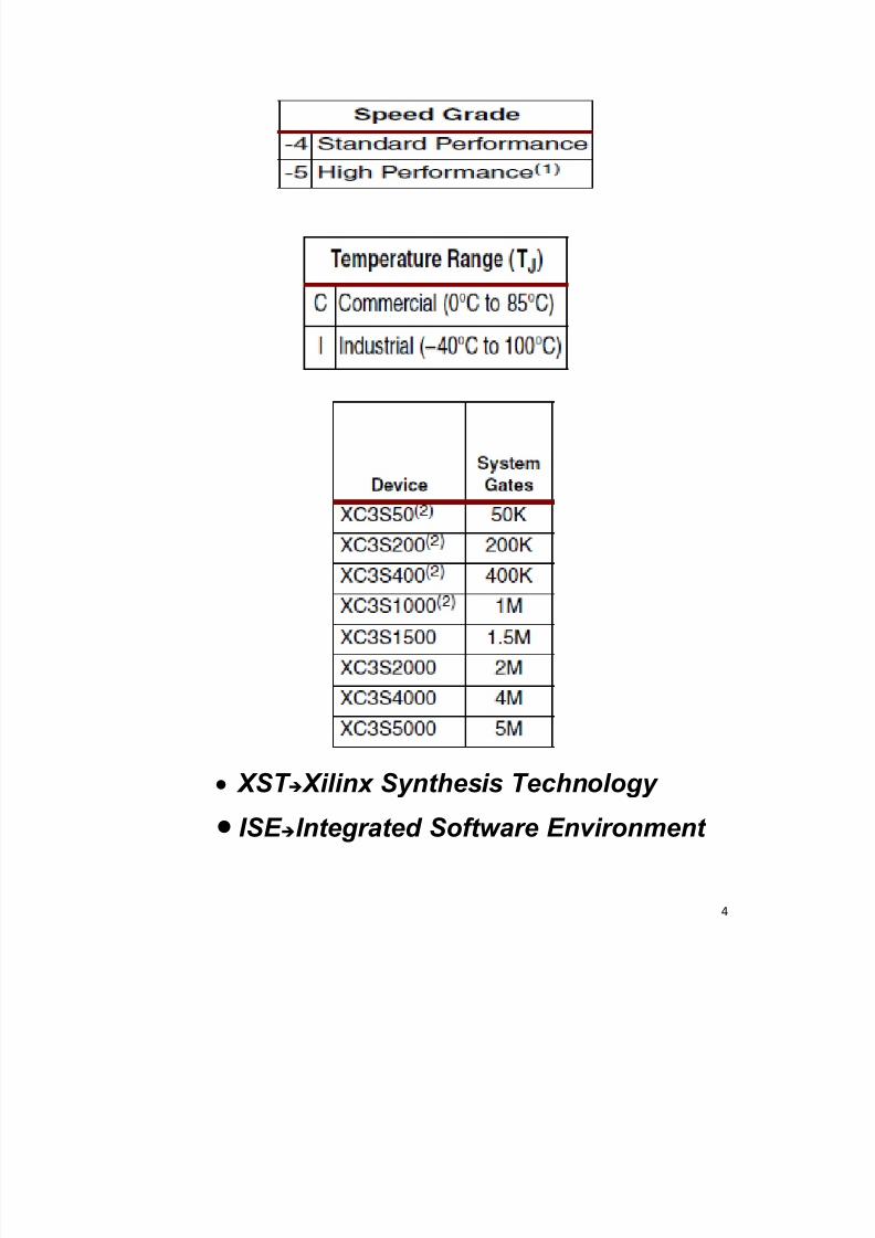
XST Xilinx Synthesis Technology
ISE Integrated Software Environment
7/31/2019 Xilinx-hdl Tool Flow
http://slidepdf.com/reader/full/xilinx-hdl-tool-flow 5/37
5
Xilinx Tool Flow
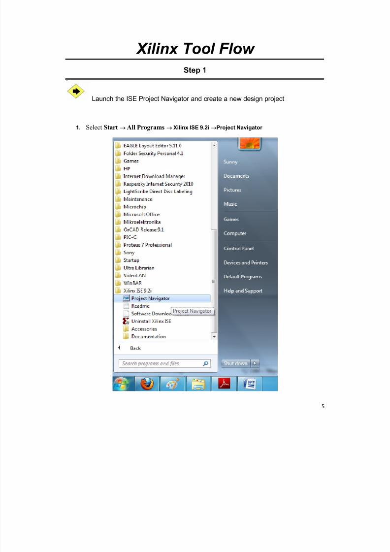
Step 1.
Launch the ISE Project Navigator and create a new design project
1. Select Start All Programs Xilinx ISE 9.2i Project Navigator
7/31/2019 Xilinx-hdl Tool Flow
http://slidepdf.com/reader/full/xilinx-hdl-tool-flow 6/37
6
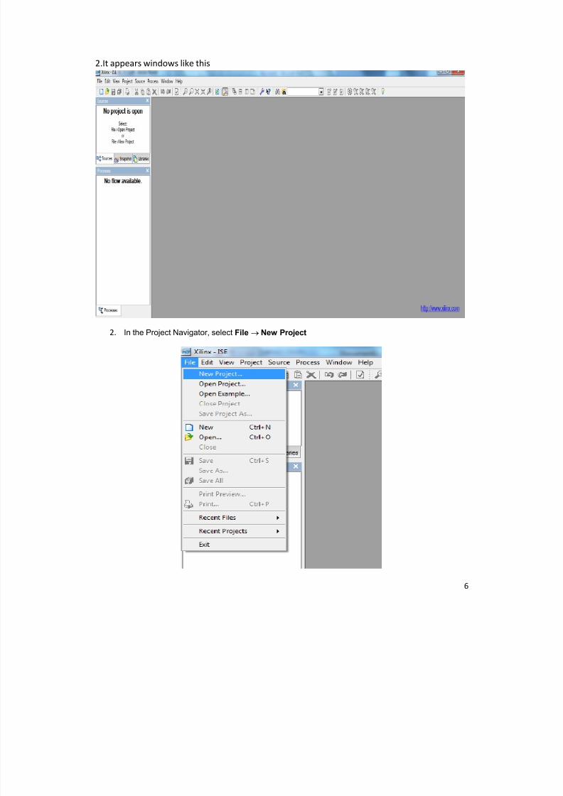
2.It appears windows like this
2. In the Project Navigator, select File New Project
7/31/2019 Xilinx-hdl Tool Flow
http://slidepdf.com/reader/full/xilinx-hdl-tool-flow 7/37
7
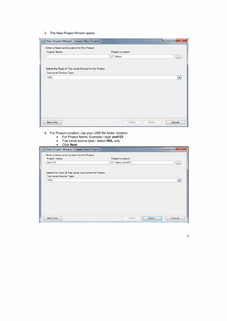
3. The New Project Wizard opens
4. For Project Location, use your USN file folder location
For Project Name, Example---type and123
Top-Level source type-- select HDL only
Click Next
7/31/2019 Xilinx-hdl Tool Flow
http://slidepdf.com/reader/full/xilinx-hdl-tool-flow 8/37
8
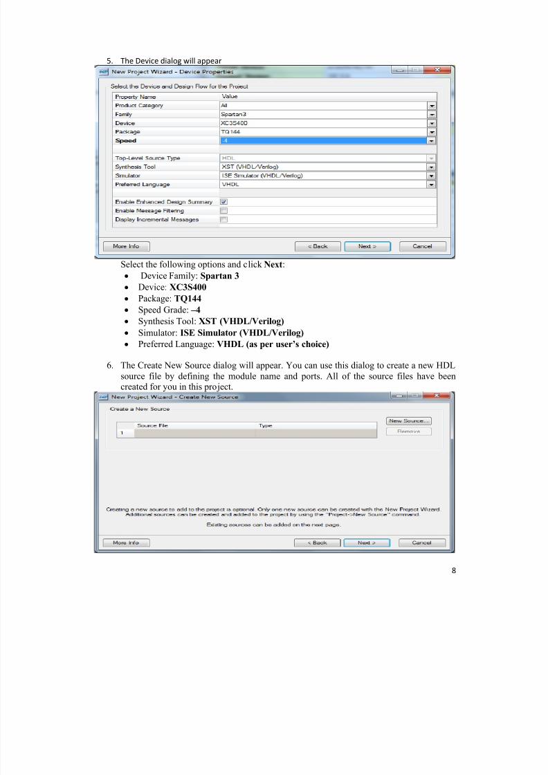
5. The Device dialog will appear
Select the following options and click Next:
Device Family: Spartan 3
Device: XC3S400
Package: TQ144
Speed Grade: –4
Synthesis Tool: XST (VHDL/Verilog)
Simulator: ISE Simulator (VHDL/Verilog)
Preferred Language: VHDL (as per user’s choice)
6. The Create New Source dialog will appear. You can use this dialog to create a new HDL
source file by defining the module name and ports. All of the source files have beencreated for you in this project.
7/31/2019 Xilinx-hdl Tool Flow
http://slidepdf.com/reader/full/xilinx-hdl-tool-flow 9/37
9
Creating a Design Step 2
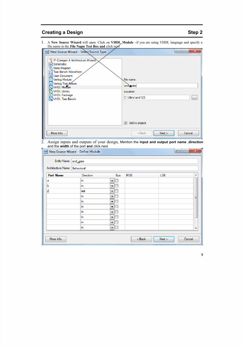
1. A New Source Wizard will open. Click on VHDL Module – if you are using VHDL language and specify afile name in the File Name Test Box and click next
2. Assign inputs and outputs of your design, Mention the input and output port name ,direction
and the width of the port and click next
7/31/2019 Xilinx-hdl Tool Flow
http://slidepdf.com/reader/full/xilinx-hdl-tool-flow 10/37
10
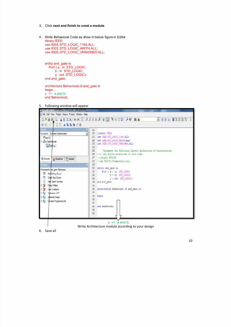
3. Click next and finish to creat a module.
4. Write Behavioral Code as show in below figure in Editor library IEEE;use IEEE.STD_LOGIC_1164.ALL;
use IEEE.STD_LOGIC_ARITH.ALL;use IEEE.STD_LOGIC_UNSIGNED.ALL;
entity and_gate isPort ( a : in STD_LOGIC;
b : in STD_LOGIC;y : out STD_LOGIC);
end and_gate;
architecture Behavioral of and_gate isbeginy <= a and b;end Behavioral;.
5. Following window will appear
y <= a and b;
Write Architecture module according to your design
6. Save all
7/31/2019 Xilinx-hdl Tool Flow
http://slidepdf.com/reader/full/xilinx-hdl-tool-flow 11/37
11
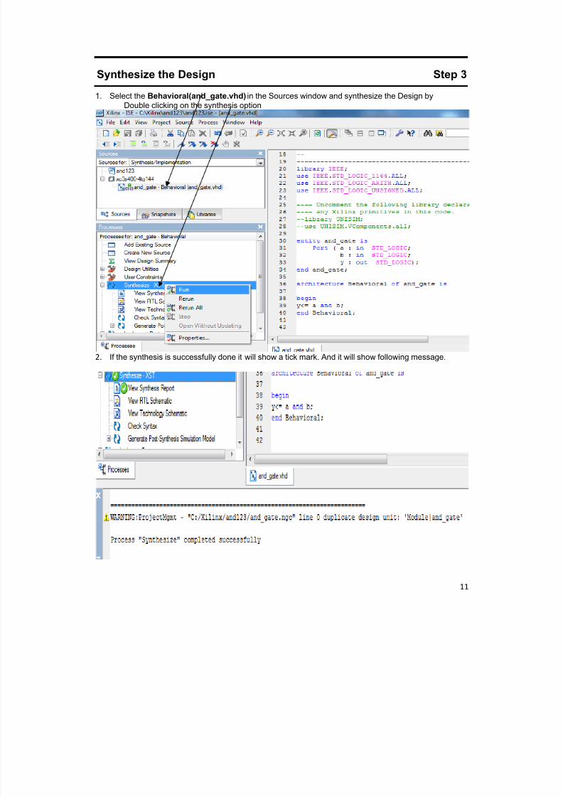
Synthesize the Design Step 3
1. Select the Behavioral(and_gate.vhd) in the Sources window and synthesize the Design byDouble clicking on the synthesis option
2. If the synthesis is successfully done it will show a tick mark. And it will show following message.
7/31/2019 Xilinx-hdl Tool Flow
http://slidepdf.com/reader/full/xilinx-hdl-tool-flow 12/37
12
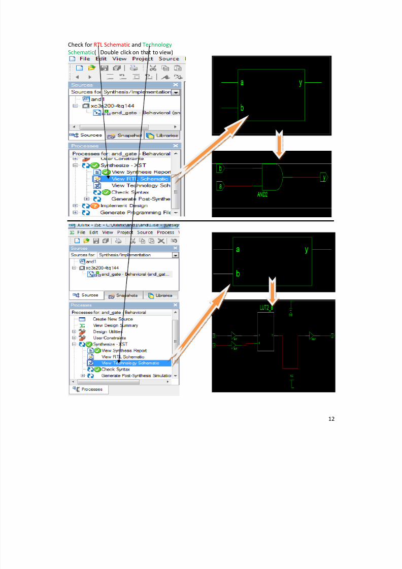
Check for RTL Schematic and Technology
Schematic( Double click on that to view)
7/31/2019 Xilinx-hdl Tool Flow
http://slidepdf.com/reader/full/xilinx-hdl-tool-flow 13/37
13
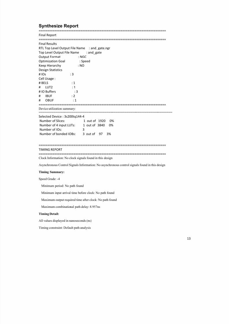
Synthesize Report
=========================================================================
Final Report
=========================================================================
Final Results
RTL Top Level Output File Name : and_gate.ngrTop Level Output File Name : and_gate
Output Format : NGC
Optimization Goal : Speed
Keep Hierarchy : NO
Design Statistics
# IOs : 3
Cell Usage :
# BELS : 1
# LUT2 : 1
# IO Buffers : 3
# IBUF : 2
# OBUF : 1
=========================================================================
Device utilization summary:
=========================================================================
Selected Device : 3s200tq144-4
Number of Slices: 1 out of 1920 0%
Number of 4 input LUTs: 1 out of 3840 0%
Number of IOs: 3
Number of bonded IOBs: 3 out of 97 3%
=========================================================================
TIMING REPORT
=========================================================================
Clock Information: No clock signals found in this design
Asynchronous Control Signals Information: No asynchronous control signals found in this design
Timing Summary:
Speed Grade: -4
Minimum period: No path found
Minimum input arrival time before clock: No path found
Maximum output required time after clock: No path found
Maximum combinational path delay: 8.957ns
Timing Detail:
All values displayed in nanoseconds (ns)
Timing constraint: Default path analysis
7/31/2019 Xilinx-hdl Tool Flow
http://slidepdf.com/reader/full/xilinx-hdl-tool-flow 14/37
14
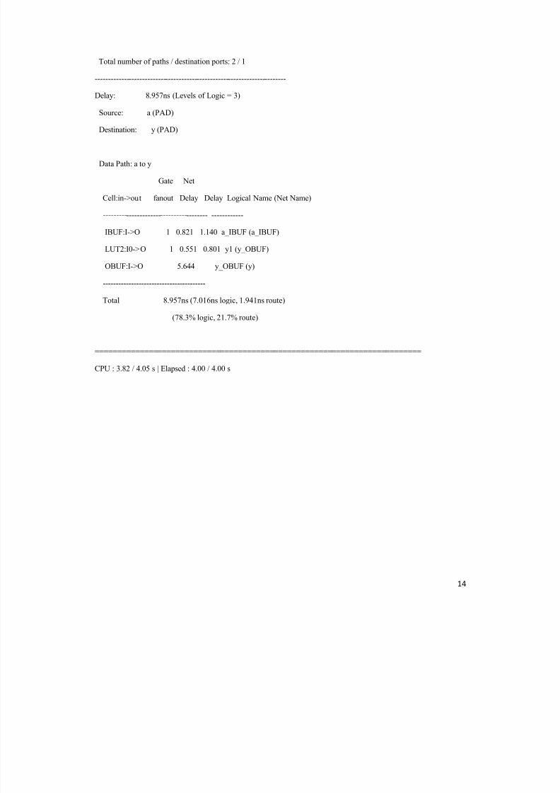
Total number of paths / destination ports: 2 / 1
-------------------------------------------------------------------------
Delay: 8.957ns (Levels of Logic = 3)
Source: a (PAD)
Destination: y (PAD)
Data Path: a to y
Gate Net
Cell:in->out fanout Delay Delay Logical Name (Net Name)
---------------------------------------- ------------
IBUF:I->O 1 0.821 1.140 a_IBUF (a_IBUF)
LUT2:I0->O 1 0.551 0.801 y1 (y_OBUF)
OBUF:I->O 5.644 y_OBUF (y)
----------------------------------------
Total 8.957ns (7.016ns logic, 1.941ns route)
(78.3% logic, 21.7% route)
=========================================================================
CPU : 3.82 / 4.05 s | Elapsed : 4.00 / 4.00 s
7/31/2019 Xilinx-hdl Tool Flow
http://slidepdf.com/reader/full/xilinx-hdl-tool-flow 15/37
15
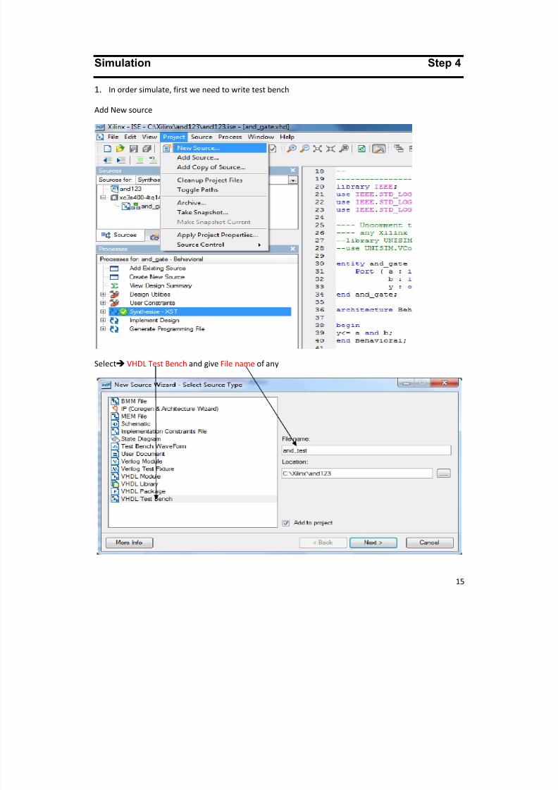
Simulation Step 4
1. In order simulate, first we need to write test bench
Add New source
Select VHDL Test Bench and give File name of any
7/31/2019 Xilinx-hdl Tool Flow
http://slidepdf.com/reader/full/xilinx-hdl-tool-flow 16/37
16
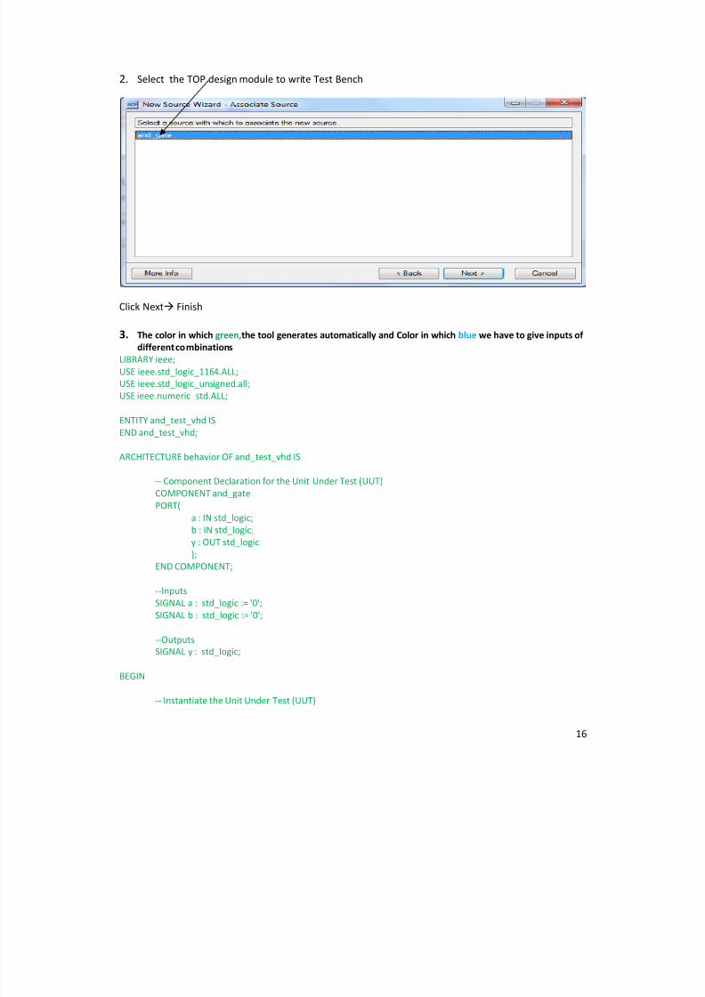
2. Select the TOP design module to write Test Bench
Click Next Finish
3. The color in which green,the tool generates automatically and Color in which blue we have to give inputs of
different combinations
LIBRARY ieee;
USE ieee.std_logic_1164.ALL;
USE ieee.std_logic_unsigned.all;
USE ieee.numeric_std.ALL;
ENTITY and_test_vhd IS
END and_test_vhd;
ARCHITECTURE behavior OF and_test_vhd IS
-- Component Declaration for the Unit Under Test (UUT)
COMPONENT and_gate
PORT(
a : IN std_logic;
b : IN std_logic;
y : OUT std_logic
);
END COMPONENT;
--Inputs
SIGNAL a : std_logic := '0';
SIGNAL b : std_logic := '0';
--Outputs
SIGNAL y : std_logic;
BEGIN
-- Instantiate the Unit Under Test (UUT)
7/31/2019 Xilinx-hdl Tool Flow
http://slidepdf.com/reader/full/xilinx-hdl-tool-flow 17/37
17
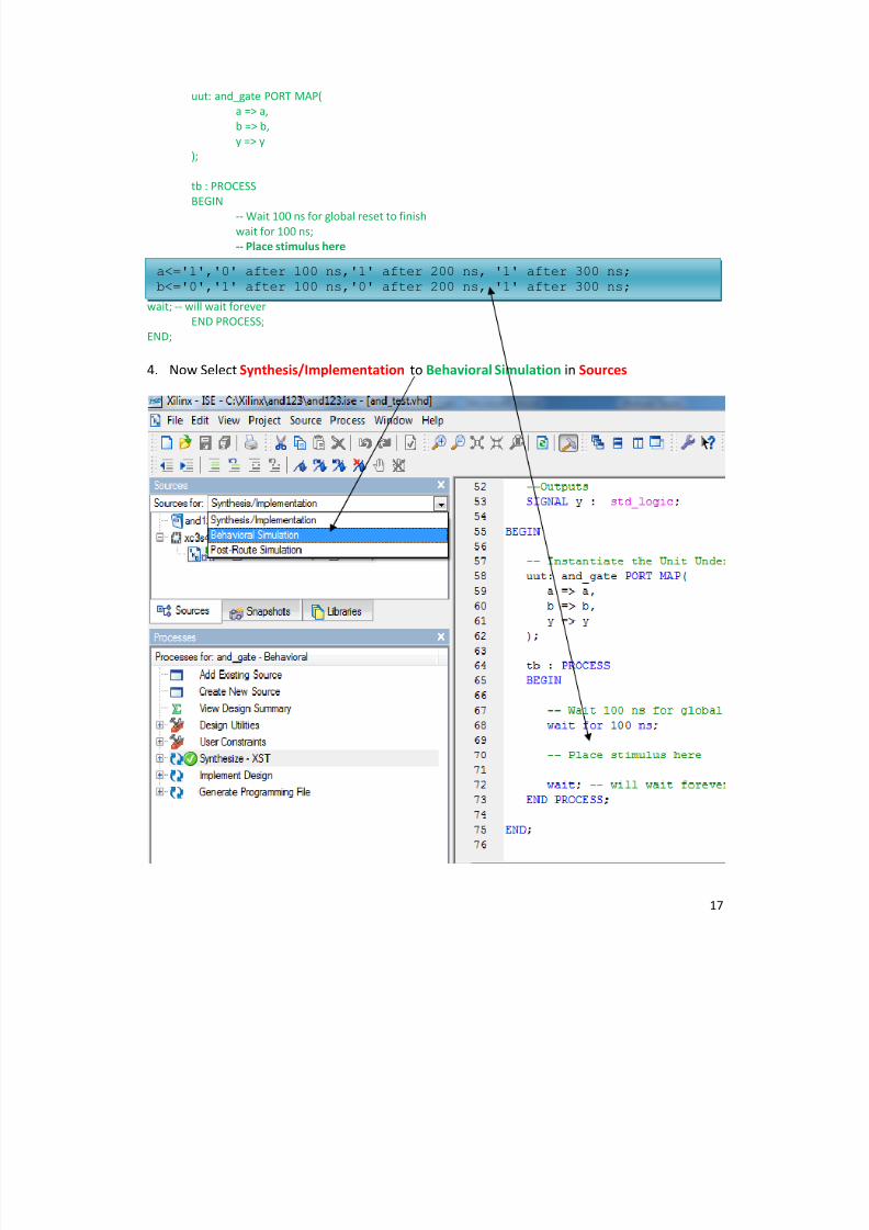
uut: and_gate PORT MAP(
a => a,
b => b,
y => y
);
tb : PROCESSBEGIN
-- Wait 100 ns for global reset to finish
wait for 100 ns;
-- Place stimulus here
wait; -- will wait forever
END PROCESS;
END;
4. Now Select Synthesis/Implementation to Behavioral Simulation in Sources
a<='1','0' after 100 ns,'1' after 200 ns, '1' after 300 ns;
b<='0','1' after 100 ns,'0' after 200 ns, '1' after 300 ns;
7/31/2019 Xilinx-hdl Tool Flow
http://slidepdf.com/reader/full/xilinx-hdl-tool-flow 18/37
18
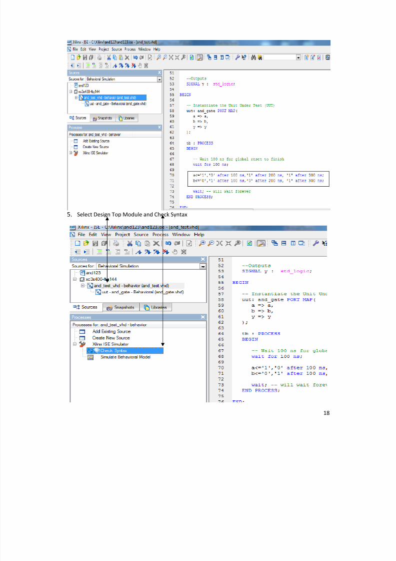
5. Select Design Top Module and Check Syntax
7/31/2019 Xilinx-hdl Tool Flow
http://slidepdf.com/reader/full/xilinx-hdl-tool-flow 19/37
19
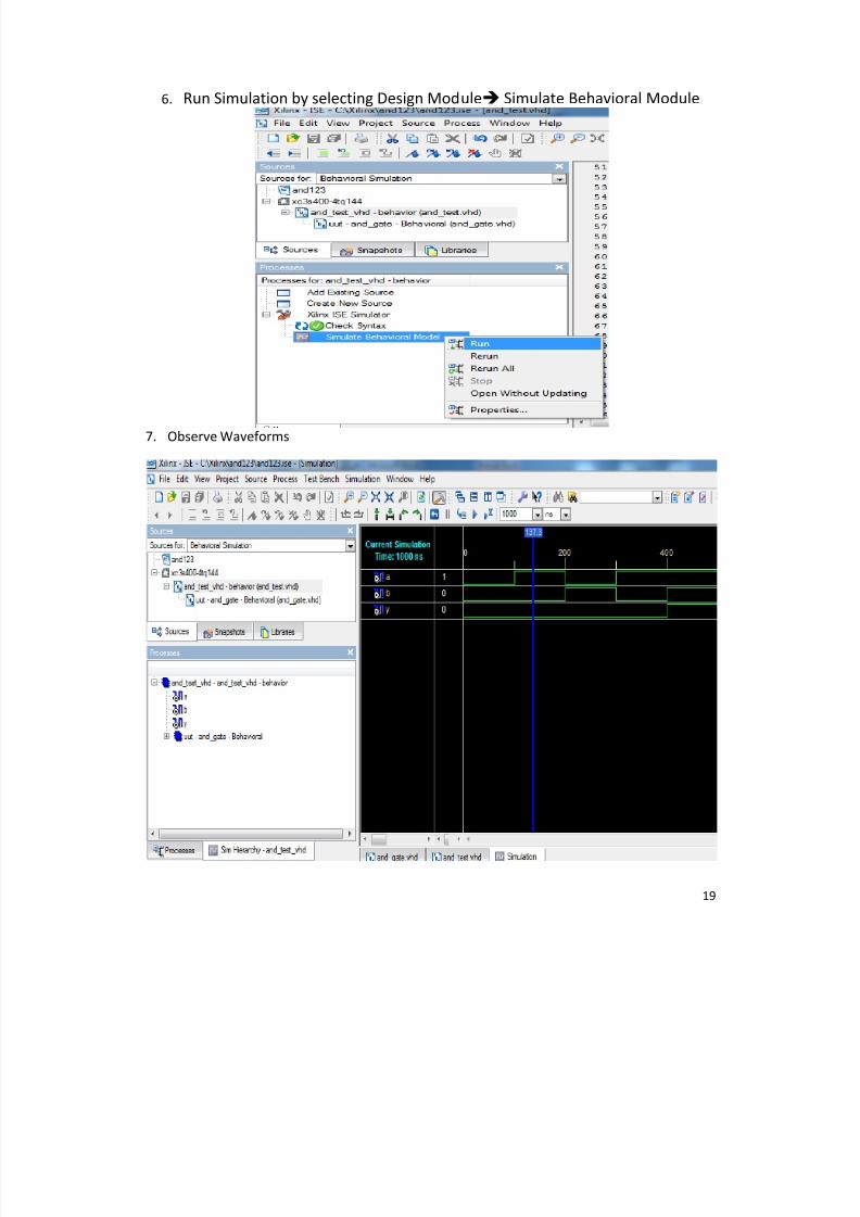
6. Run Simulation by selecting Design Module Simulate Behavioral Module
7. Observe Waveforms
7/31/2019 Xilinx-hdl Tool Flow
http://slidepdf.com/reader/full/xilinx-hdl-tool-flow 20/37
20
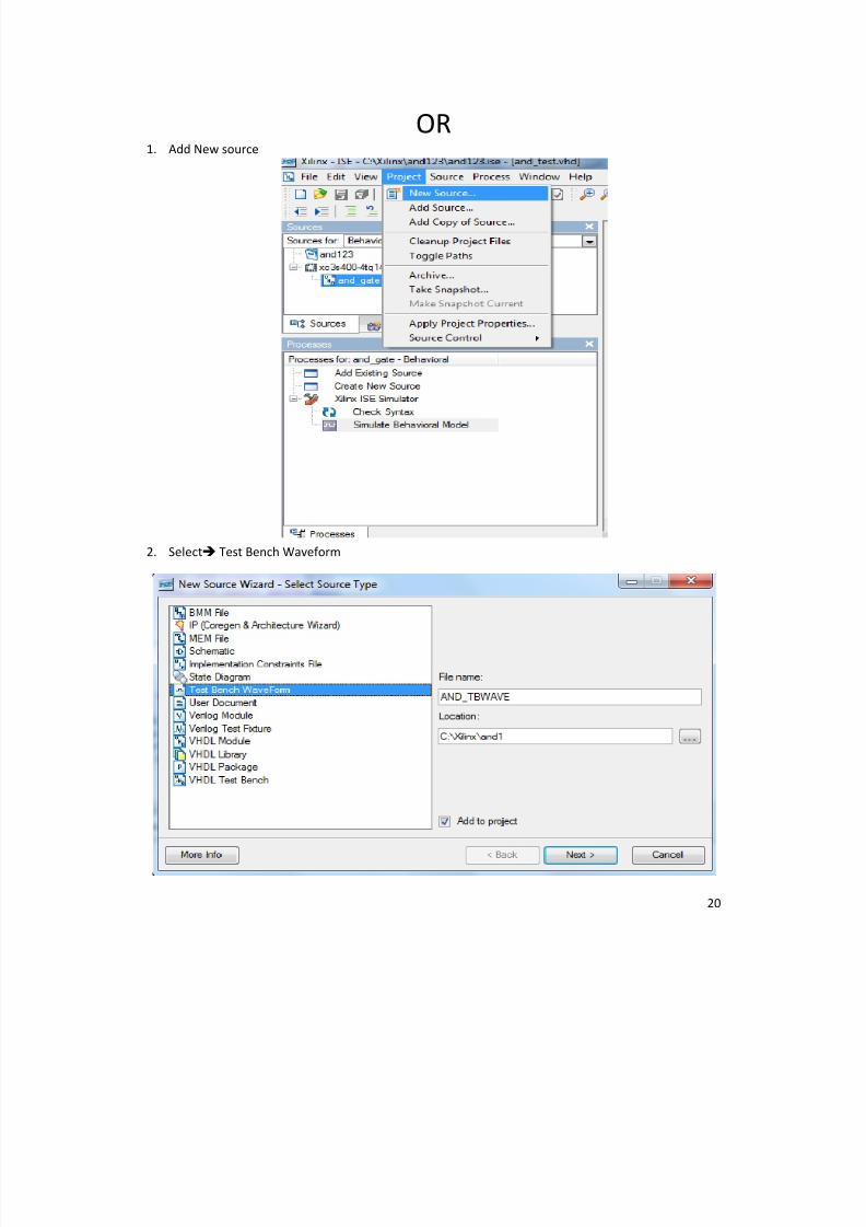
OR1. Add New source
2. Select Test Bench Waveform
7/31/2019 Xilinx-hdl Tool Flow
http://slidepdf.com/reader/full/xilinx-hdl-tool-flow 21/37
21
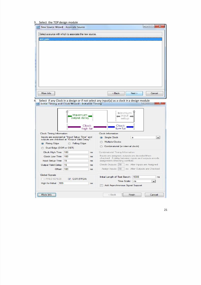
3. Select the TOP design module
4. Select if any Clock in a design or if not select any input(a) as a clock in a design module
7/31/2019 Xilinx-hdl Tool Flow
http://slidepdf.com/reader/full/xilinx-hdl-tool-flow 22/37
22
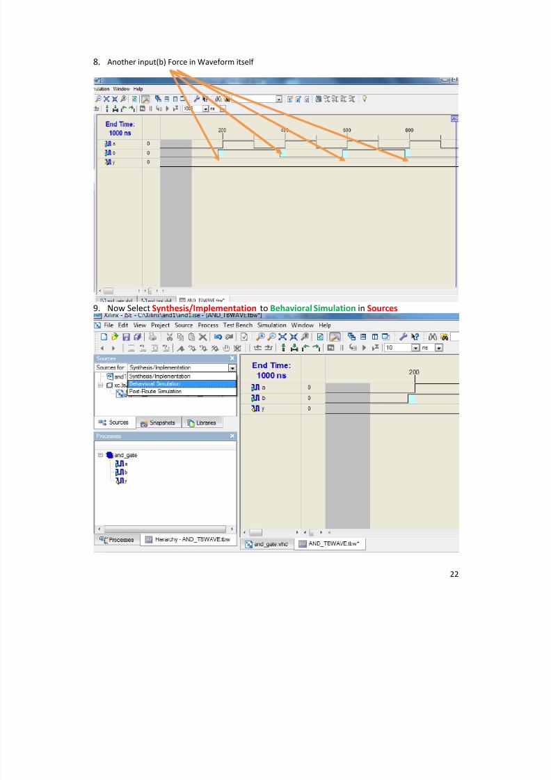
8. Another input(b) Force in Waveform itself
9. Now Select Synthesis/Implementation to Behavioral Simulation in Sources
7/31/2019 Xilinx-hdl Tool Flow
http://slidepdf.com/reader/full/xilinx-hdl-tool-flow 23/37
23
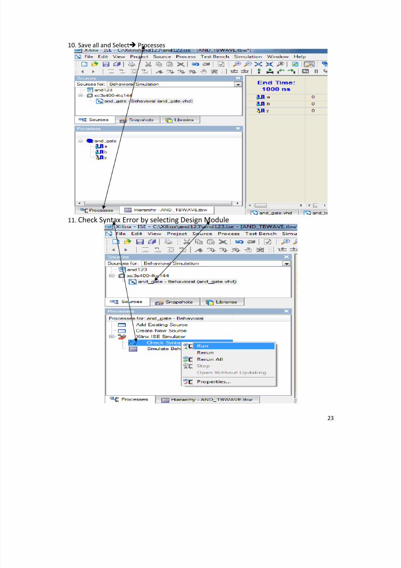
10. Save all and Select Processes
11. Check Syntax Error by selecting Design Module
7/31/2019 Xilinx-hdl Tool Flow
http://slidepdf.com/reader/full/xilinx-hdl-tool-flow 24/37
24
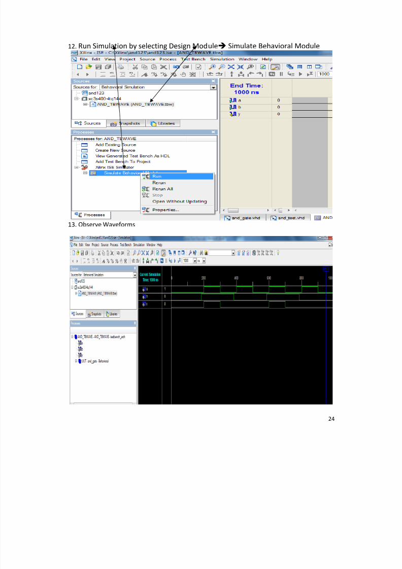
12. Run Simulation by selecting Design Module Simulate Behavioral Module
13. Observe Waveforms
7/31/2019 Xilinx-hdl Tool Flow
http://slidepdf.com/reader/full/xilinx-hdl-tool-flow 25/37
25
Testing on Hardware Kit Step-5
Procedure:
Software part
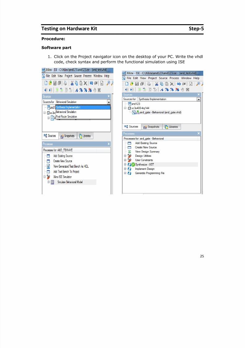
1. Click on the Project navigator icon on the desktop of your PC. Write the vhdl
code, check syntax and perform the functional simulation using ISE
7/31/2019 Xilinx-hdl Tool Flow
http://slidepdf.com/reader/full/xilinx-hdl-tool-flow 26/37
26
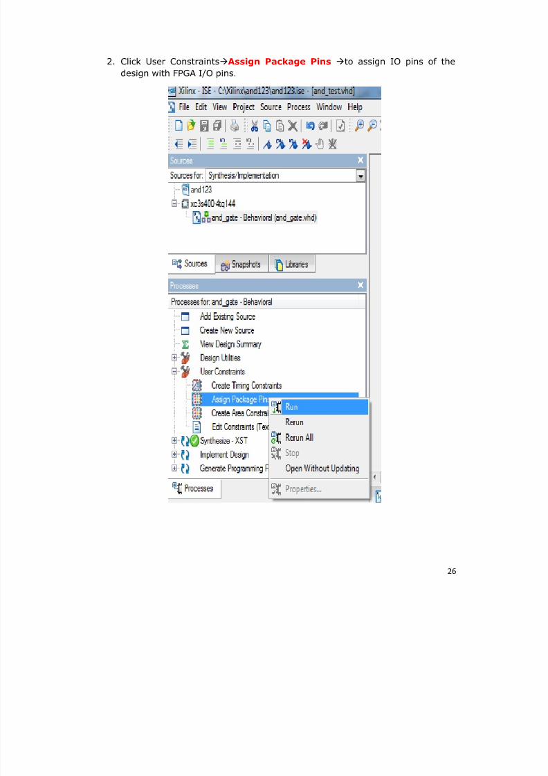
2. Click User ConstraintsAssign Package Pins to assign IO pins of the
design with FPGA I/O pins.
7/31/2019 Xilinx-hdl Tool Flow
http://slidepdf.com/reader/full/xilinx-hdl-tool-flow 27/37
27
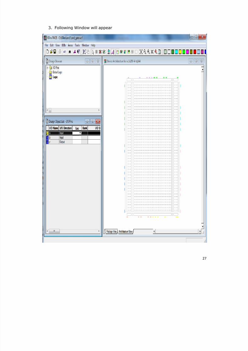
3. Following Window will appear
7/31/2019 Xilinx-hdl Tool Flow
http://slidepdf.com/reader/full/xilinx-hdl-tool-flow 28/37
HDL LAB MANUAL SUNIL MP
28
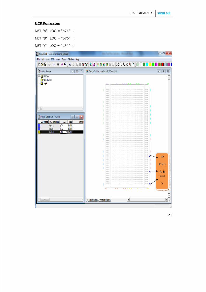
UCF For gates
NET "A" LOC = "p74" ;
NET "B" LOC = "p76" ;
NET "Y" LOC = "p84" ;
IO
PIN’s
A, B
and
Y
7/31/2019 Xilinx-hdl Tool Flow
http://slidepdf.com/reader/full/xilinx-hdl-tool-flow 29/37
HDL LAB MANUAL SUNIL MP
29
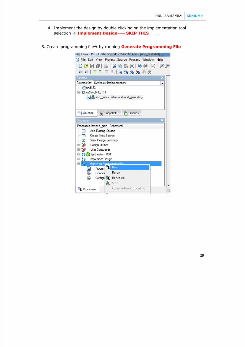
4. Implement the design by double clicking on the implementation tool
selection Implement Design---- SKIP THIS
5. Create programming file by running Generate Programming File
7/31/2019 Xilinx-hdl Tool Flow
http://slidepdf.com/reader/full/xilinx-hdl-tool-flow 30/37
HDL LAB MANUAL SUNIL MP
30
Hardware part
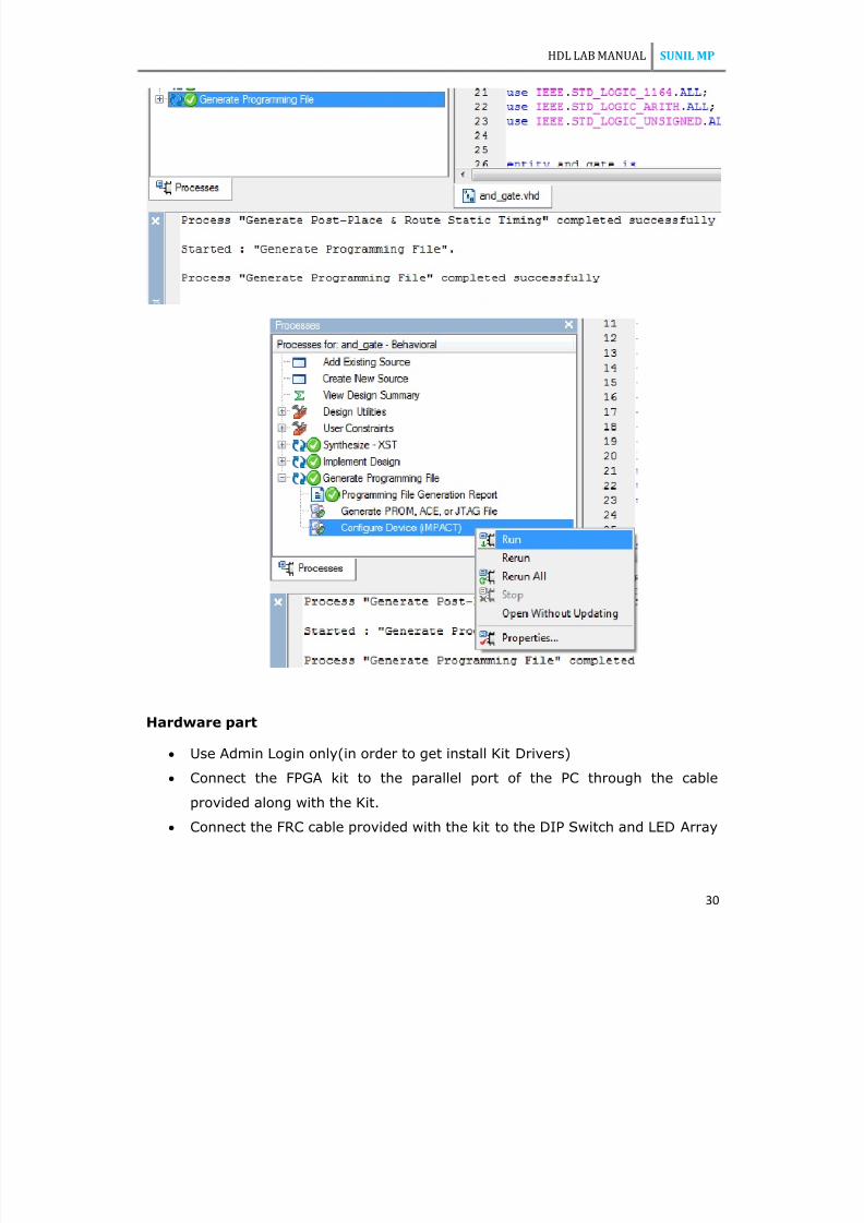
Use Admin Login only(in order to get install Kit Drivers)
Connect the FPGA kit to the parallel port of the PC through the cable
provided along with the Kit.
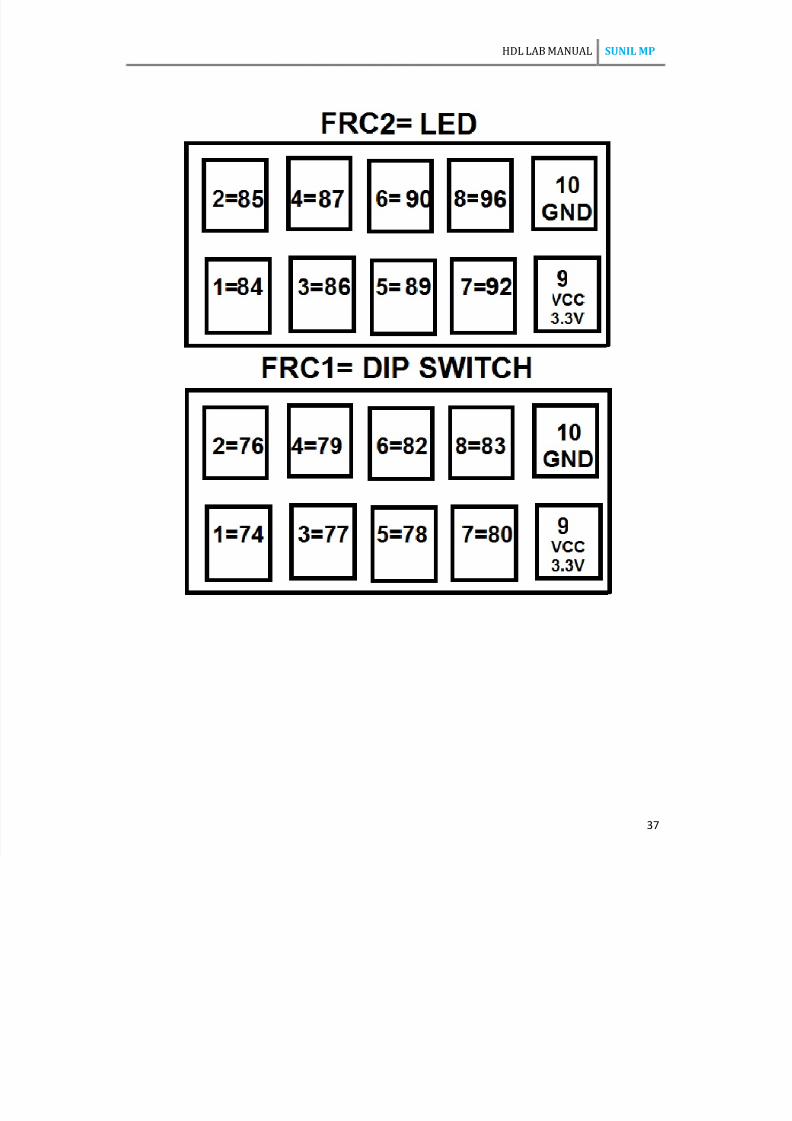
Connect the FRC cable provided with the kit to the DIP Switch and LED Array
7/31/2019 Xilinx-hdl Tool Flow
http://slidepdf.com/reader/full/xilinx-hdl-tool-flow 31/37
HDL LAB MANUAL SUNIL MP
31
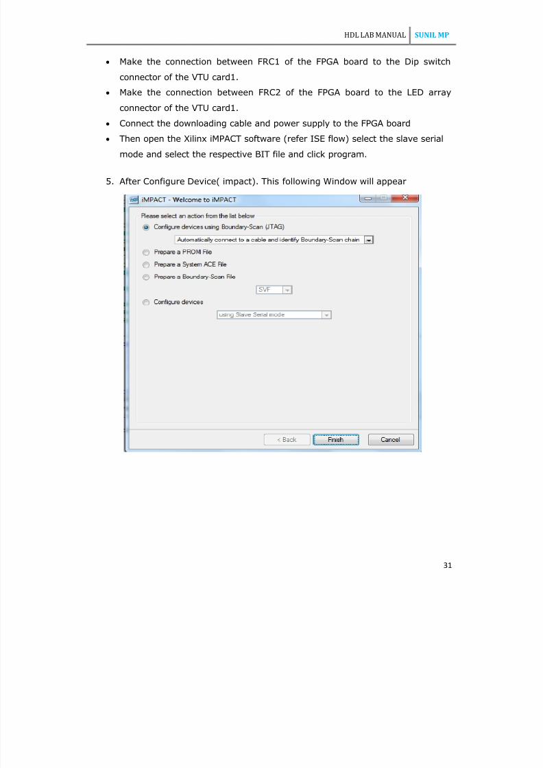
Make the connection between FRC1 of the FPGA board to the Dip switch
connector of the VTU card1.
Make the connection between FRC2 of the FPGA board to the LED array
connector of the VTU card1.
Connect the downloading cable and power supply to the FPGA board
Then open the Xilinx iMPACT software (refer ISE flow) select the slave serial
mode and select the respective BIT file and click program.
5. After Configure Device( impact). This following Window will appear
7/31/2019 Xilinx-hdl Tool Flow
http://slidepdf.com/reader/full/xilinx-hdl-tool-flow 32/37
HDL LAB MANUAL SUNIL MP
32
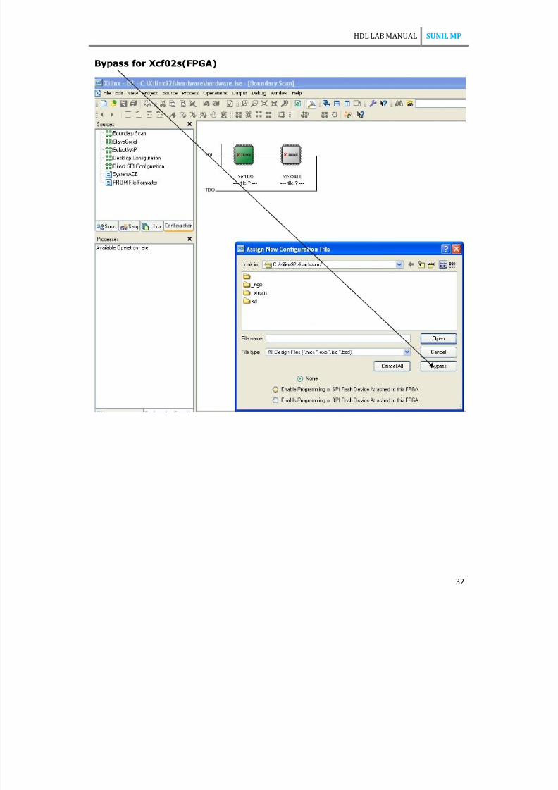
Bypass for Xcf02s(FPGA)
7/31/2019 Xilinx-hdl Tool Flow
http://slidepdf.com/reader/full/xilinx-hdl-tool-flow 33/37
HDL LAB MANUAL SUNIL MP
33
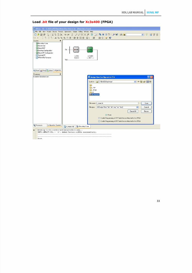
Load .bit file of your design for Xc3s400 (FPGA)
7/31/2019 Xilinx-hdl Tool Flow
http://slidepdf.com/reader/full/xilinx-hdl-tool-flow 34/37
HDL LAB MANUAL SUNIL MP
34
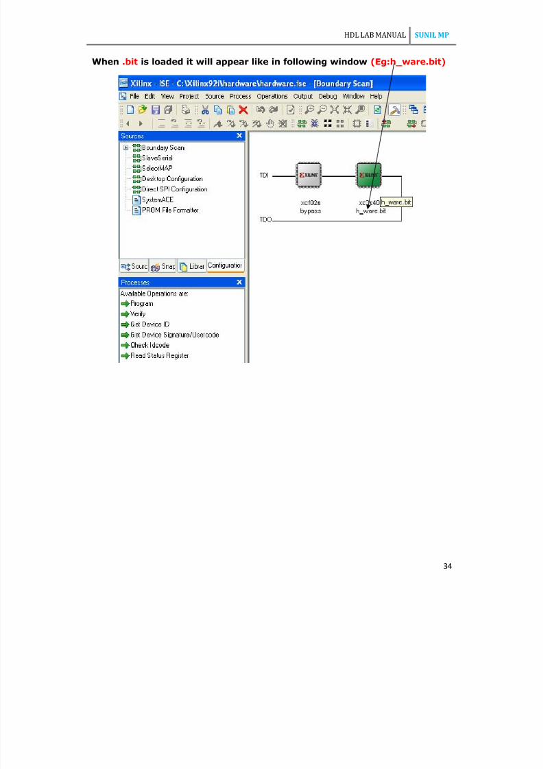
When .bit is loaded it will appear like in following window (Eg:h_ware.bit)
7/31/2019 Xilinx-hdl Tool Flow
http://slidepdf.com/reader/full/xilinx-hdl-tool-flow 35/37
HDL LAB MANUAL SUNIL MP
35
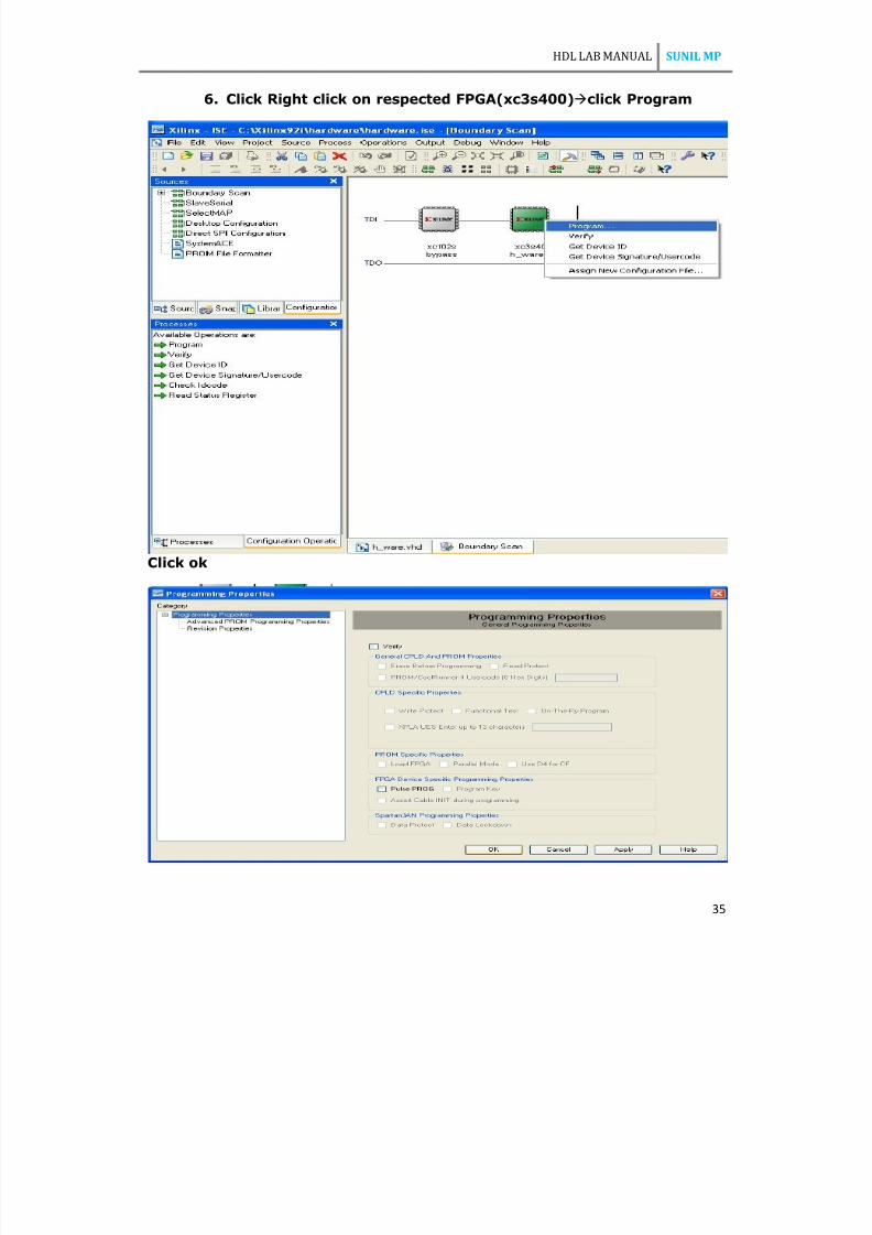
6. Click Right click on respected FPGA(xc3s400)click Program
Click ok
7/31/2019 Xilinx-hdl Tool Flow
http://slidepdf.com/reader/full/xilinx-hdl-tool-flow 36/37
HDL LAB MANUAL SUNIL MP
36
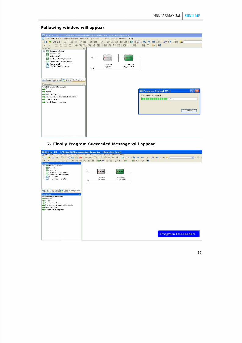
Following window will appear
7. Finally Program Succeeded Message will appear
7/31/2019 Xilinx-hdl Tool Flow
http://slidepdf.com/reader/full/xilinx-hdl-tool-flow 37/37
HDL LAB MANUAL SUNIL MP