Embed Size (px)
Citation preview
9
8
7
6
5
4
3
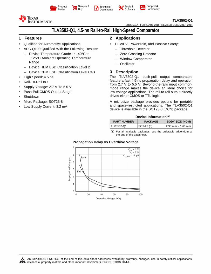
Pro
pa
gatio
nD
ela
y(n
s)
0 10040 60 8020
Overdrive Voltage (mV)
Fall
Rise
VCM = 1 V
VS = 5 V
CLOAD = 17 pF
Product
Folder
Sample &Buy
Technical
Documents
Tools &
Software
Support &Community
TLV3502-Q1SBOS507A –FEBRUARY 2010–REVISED DECEMBER 2014
TLV3502-Q1, 4.5-ns Rail-to-Rail High-Speed Comparator1 Features 2 Applications1• Qualified for Automotive Applications • HEV/EV, Powertrain, and Passive Safety:• AEC-Q100 Qualified With the Following Results: – Threshold Detector
– Device Temperature Grade 1: –40°C to – Zero-Crossing Detector+125°C Ambient Operating Temperature – Window ComparatorRange – Oscillator
– Device HBM ESD Classification Level 2– Device CDM ESD Classification Level C4B 3 Description
The TLV3502-Q1 push-pull output comparators• High Speed: 4.5 nsfeature a fast 4.5-ns propagation delay and operation• Rail-To-Rail I/Ofrom 2.7 V to 5.5 V. Beyond-the-rails input common-
• Supply Voltage: 2.7 V To 5.5 V mode range makes the device an ideal choice for• Push-Pull CMOS Output Stage low-voltage applications. The rail-to-rail output directly
drives either CMOS or TTL logic.• Shutdown• Micro Package: SOT23-8 A microsize package provides options for portable
and space-restricted applications. The TLV3502-Q1• Low Supply Current: 3.2 mAdevice is available in the SOT23-8 (DCN) package.
Device Information(1)
PART NUMBER PACKAGE BODY SIZE (NOM)TLV3502-Q1 SOT-23 (8) 2.90 mm × 1.60 mm
(1) For all available packages, see the orderable addendum atthe end of the datasheet.
Propagation Delay vs Overdrive Voltage
1
An IMPORTANT NOTICE at the end of this data sheet addresses availability, warranty, changes, use in safety-critical applications,intellectual property matters and other important disclaimers. PRODUCTION DATA.
TLV3502-Q1SBOS507A –FEBRUARY 2010–REVISED DECEMBER 2014 www.ti.com
Table of Contents7.2 Functional Block Diagram ......................................... 91 Features .................................................................. 17.3 Feature Description................................................... 92 Applications ........................................................... 17.4 Device Functional Modes........................................ 113 Description ............................................................. 1
8 Application and Implementation ........................ 124 Revision History..................................................... 28.1 Application Information............................................ 125 Pin Configuration and Functions ......................... 38.2 Typical Application ................................................. 126 Specifications......................................................... 4
9 Power Supply Recommendations ...................... 136.1 Absolute Maximum Ratings ...................................... 410 Layout................................................................... 136.2 ESD Ratings ............................................................ 4
10.1 Layout Guidelines ................................................. 136.3 Recommended Operating Conditions....................... 410.2 Layout Example .................................................... 146.4 Thermal Information ................................................. 4
11 Device and Documentation Support ................. 166.5 Electrical Characteristics........................................... 511.1 Trademarks ........................................................... 166.6 Switching Characteristics .......................................... 511.2 Electrostatic Discharge Caution............................ 166.7 Typical Characteristics .............................................. 611.3 Glossary ................................................................ 167 Detailed Description .............................................. 9
12 Mechanical, Packaging, and Orderable7.1 Overview ................................................................... 9Information ........................................................... 16
4 Revision History
Changes from Original (February 2010) to Revision A Page
• Deleted references to the TLV3501 device and changed the TLV3502 device name to TLV3502-Q1 ................................ 1• Added ESD Ratings table, Feature Description section, Device Functional Modes, Application and Implementation
section, Power Supply Recommendations section, Layout section, Device and Documentation Support section, andMechanical, Packaging, and Orderable Information section ................................................................................................. 4
2 Submit Documentation Feedback Copyright © 2010–2014, Texas Instruments Incorporated
Product Folder Links: TLV3502-Q1
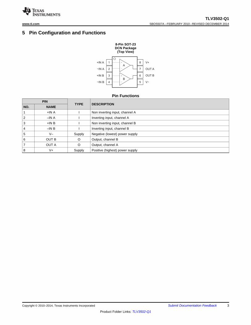
1
2
3
4
8
7
6
5
V+
OUT A
OUT B
V−
+IN A
−IN A
+IN B
−IN B
A
B
TLV3502-Q1www.ti.com SBOS507A –FEBRUARY 2010–REVISED DECEMBER 2014
5 Pin Configuration and Functions
8-Pin SOT-23DCN Package
(Top View)
Pin FunctionsPIN
TYPE DESCRIPTIONNO. NAME1 +IN A I Non inverting input, channel A2 –IN A I Inverting input, channel A3 +IN B I Non inverting input, channel B4 –IN B I Inverting input, channel B5 V– Supply Negative (lowest) power supply6 OUT B O Output, channel B7 OUT A O Output, channel A8 V+ Supply Positive (highest) power supply
Copyright © 2010–2014, Texas Instruments Incorporated Submit Documentation Feedback 3
Product Folder Links: TLV3502-Q1
TLV3502-Q1SBOS507A –FEBRUARY 2010–REVISED DECEMBER 2014 www.ti.com
6 Specifications
6.1 Absolute Maximum Ratingsover operating free-air temperature range (unless otherwise noted) (1)
MIN MAX UNITSupply voltage 5.5 VSignal input terminal voltage (2) (V−) − 0.3 (V+) + 0.3 VSignal input terminal current (2) 10 mAOutput short-circuit current (3) 74 mAThermal impedance, junction to free air 200 200 °C/WOperating temperature −40 125 °CJunction temperature 150 °CStorage temperature, Tstg −65 150 °C
(1) Stresses beyond those listed under Absolute Maximum Ratings may cause permanent damage to the device. These are stress ratingsonly, which do not imply functional operation of the device at these or any other conditions beyond those indicated under RecommendedOperating Conditions. Exposure to absolute-maximum-rated conditions for extended periods may affect device reliability.
(2) Input terminals are diode-clamped to the power-supply rails. Input signals that can swing more than 0.3 V beyond the supply rails shouldbe current limited to 10mA or less.
(3) Short circuit to ground, one comparator per package
6.2 ESD RatingsVALUE UNIT
Human body model (HBM), per AEC Q100-002 (1) ±2000Corner pins (+IN A, –IN B, V+, and ±750V(ESD) Electrostatic discharge VCharged device model (CDM), per AEC V–)
Q100-011Other pins ±500
(1) AEC Q100-002 indicates HBM stressing is done in accordance with the ANSI/ESDA/JEDEC JS-001 specification.
6.3 Recommended Operating Conditionsover operating free-air temperature range (unless otherwise noted)
MIN NOM MAX UNITVS Supply voltage 2.2 2.7 5.5 V
(V+) -VIL Low-level input voltage, shutdown (comparator is enabled) (1) V1.7VIH High-level input voltage, shutdown (comparator is disabled) (1) (V+) – 0.9 VTA Operating temperature –40 125 °C
(1) When the shutdown pin is within 0.9 V of the most positive supply, the part is disabled. When it is more than 1.7 V below the mostpositive supply, the part is enabled.
6.4 Thermal InformationTLV3502-Q1
THERMAL METRIC (1) SOT-23 UNIT8 PINS
RθJA Junction-to-ambient thermal resistance 191.6RθJC(top) Junction-to-case (top) thermal resistance 43.9RθJB Junction-to-board thermal resistance 120.3 °C/WψJT Junction-to-top characterization parameter 14.4ψJB Junction-to-board characterization parameter 118.6
(1) For more information about traditional and new thermal metrics, see the IC Package Thermal Metrics application report, SPRA953.
4 Submit Documentation Feedback Copyright © 2010–2014, Texas Instruments Incorporated
Product Folder Links: TLV3502-Q1
TLV3502-Q1www.ti.com SBOS507A –FEBRUARY 2010–REVISED DECEMBER 2014
6.5 Electrical CharacteristicsTA = 25°C and VS = 2.7 V to 5.5 V (unless otherwise noted)
PARAMETER TEST CONDITIONS MIN TYP MAX UNITVOS Input offset voltage (1) VCM = 0 V, IO = 0 mA ±1 ±6.5 mVΔVOS/ΔT Offset voltage vs temperature TA = –40°C to 125°C ±5 µV/°CPSRR Offset voltage vs power supply VS = 2.7 V to 5.5 V 100 400 µV/V
Input hysteresis 6 mVIB Input bias current VCM = VCC/2, ΔVIN = ±5.5 V ±2 ±10 pAIOS Input offset current (2) VCM = VCC/2, ΔVIN = ±5.5 V ±2 ±10 pAVCM Common-mode voltage range (V–) - 0.2 (V+) + 0.2 V
VCM = –0.2 V to (V+) + 0.2 V 57 70CMRR Common-mode rejection dBTA = −40°C to 125°C 55VCM = –0.2 V to (V+) + 0.2 V
Common-mode input impedance 1013 || 2 Ω || pFDifferential input impedance 1013 || 4 Ω || pF
VOH High-level voltage output from rail IOUT = ±1 mA 30 50 mVVOL Low-level voltage output from rail IOUT = ±1 mA 30 50 mV
Input bias current of shutdown pin 2 pAIQ Quiescent current per comparator VS = 5 V, VO = High 3.2 5 mAIQ(SD) Quiescent current in shutdown 2 µA
(1) VOS is defined as the average of the positive and the negative switching thresholds.(2) The difference between IB+ and IB−.
6.6 Switching CharacteristicsTA = 25°C and VS = 2.7 V to 5.5 V (unless otherwise noted)
PARAMETER TEST CONDITIONS MIN TYP MAX UNITΔVIN = 100 mV, Overdrive = 20 mV 4.5 6.4 nsTA = −40°C to 125°C 7 nsΔVIN = 100 mV, Overdrive = 20 mV
tpd Propagation delay time (1) (2)ΔVIN = 100 mV, Overdrive = 5 mV 7.5 10 nsTA = −40°C to 125°C 12 nsΔVIN = 100 mV, Overdrive = 5 mV
Δt(SKEW) Propagation delay skew (3) ΔVIN = 100 mV, Overdrive = 20 mV 0.5 nsfMAX Maximum toggle frequency Overdrive = 50 mV, VS = 5 V 80 MHztR Rise time (4) 1.5 nstF Fall time (4) 1.5 nstOFF Shutdown turn-off time 30 nstON Shutdown turn-on time 100 ns
(1) Propagation delay cannot be accurately measured with low overdrive on automatic test equipment. This parameter is ensured bycharacterization at 100-mV overdrive.
(2) Not production tested(3) The difference between the propagation delay going high and the propagation delay going low.(4) Measured between 10% of VS and 90% of VS.
Copyright © 2010–2014, Texas Instruments Incorporated Submit Documentation Feedback 5
Product Folder Links: TLV3502-Q1
9
8
7
6
5
4
3
Pro
paga
tion
De
lay
(ns)
Rise
Fall
Capacitive Load (pF)
0 10020 40 60 80
Rise
Fall
9
8
7
6
5
4
3
Pro
pagation
De
lay
(ns)
Capacitive Load (pF)
0 10020 40 60 80
5.0
4.5
4.0
3.5
3.0
Pro
pagation
Dela
y(n
s)
Rise
Fall
Temperature (°C)
−40 100 125−25 0 25 50 75
5.0
4.5
4.0
3.5
3.0
Pro
pagation
De
lay
(ns)
Rise
Fall
Temperature (°C)
−40 100 125−25 0 25 50 75
0
5
4
3
2
1
0
−1
−10 4010 20 300
Time (ns)
Input
VOD = 100 mV VOD = 50 mV
VOD = 20 mV
VOD = 5 mV
Inp
ut
Vo
lta
ge
(V
)O
utp
ut
Vo
lta
ge
(V
)
0
5
4
3
2
1
0
−1
Input V
oltage (
V)
−10 4010 20 300
Time (ns)
Input
VOD = 100 mV
VOD = 50 mV
VOD = 20 mV
VOD = 5 mV
Outp
ut V
oltage (
V)
TLV3502-Q1SBOS507A –FEBRUARY 2010–REVISED DECEMBER 2014 www.ti.com
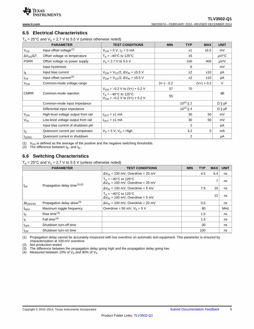
6.7 Typical CharacteristicsTA = 25°C, VS = 5 V, Input Overdrive = 100 mV (unless otherwise noted)
Figure 1. Output Response for Various Overdrive Voltages Figure 2. Output Response for Various Overdrive Voltages(rising) (falling)
VOD = 20 mV VOD = 50 mV
Figure 3. Propagation Delay vs Temperature Figure 4. Propagation Delay vs Temperature
VOD = 20 mV VOD = 50 mV
Figure 5. Propagation Delay vs Capacitive Load Figure 6. Propagation Delay vs Capacitive Load
6 Submit Documentation Feedback Copyright © 2010–2014, Texas Instruments Incorporated
Product Folder Links: TLV3502-Q1
4.0
3.8
3.6
3.4
3.2
3.0
2.8
2.6
2.4
2.2
2.0
Quie
sce
ntC
urr
ent
(mA
)
2 64 53
Supply Voltage (V)
4.0
3.8
3.6
3.4
3.2
3.0
2.8
2.6
2.4
2.2
2.0
Quie
sce
ntC
urr
ent
(mA
)
−40 −25 0 12550 75 10025
Temperature (°C)
10
0
−10
5
4
3
2
1
0
−1
0 10040 60 8020
Time (ns)
Inp
ut
Vo
lta
ge
(V
)O
utp
ut
Vo
lta
ge
(V
)
Time (ns)
500
0
−500
2
1
0
−1
−2
0 2 4 6 8 10 12 14 16 18 20
Input V
oltage (
V)
Outp
ut V
oltage (
V)
110
90
70
50
Wake−
Up
Dela
y(n
s)
WAKE−UP DELAY vs TEMPERATURE
Temperature (°C)
−40 100 125−25 0 25 50 75
9
8
7
6
5
4
3
Pro
paga
tion
De
lay
(ns)
2 64 53
Supply Voltage (V)
Rise
Fall
TLV3502-Q1www.ti.com SBOS507A –FEBRUARY 2010–REVISED DECEMBER 2014
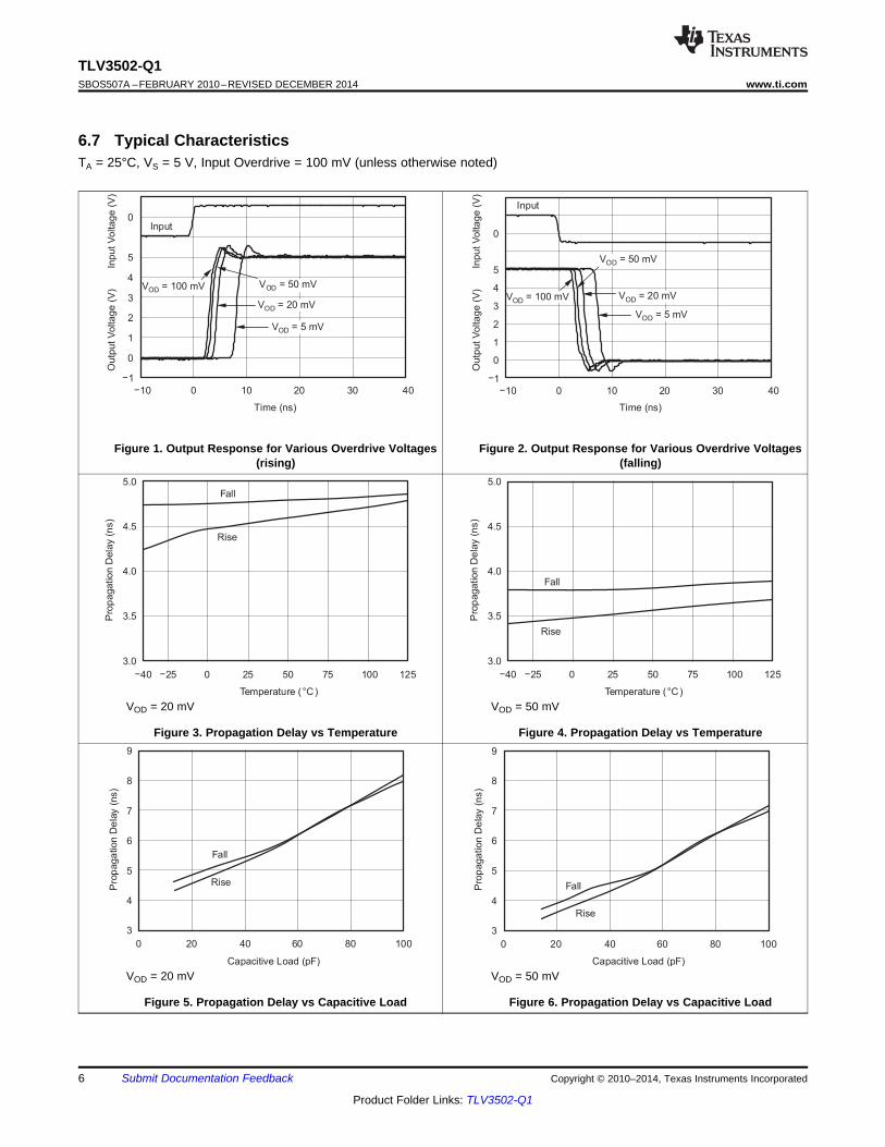
Typical Characteristics (continued)TA = 25°C, VS = 5 V, Input Overdrive = 100 mV (unless otherwise noted)
VDD = 5 V VIN = 20 mVpp
Figure 7. Propagation Delay vs Supply Voltage Figure 8. Wake-Up Delay vs Temperature
±2.5-V dual supply into 50-Ω oscilloscope inputVDD = 5 V VIN = 20 mVpp
Figure 10. Response to 100 MHz Sine WaveFigure 9. Response to 50-MHz Sine Wave
Figure 11. Quiescent Current vs Supply Voltage Figure 12. Quiescent Current vs Temperature
Copyright © 2010–2014, Texas Instruments Incorporated Submit Documentation Feedback 7
Product Folder Links: TLV3502-Q1
3.5
3.0
2.5
2.0
1.5
1.0
0.5
0
Quie
sce
ntC
urr
ent
(mA
)
0 52 3 41
Shutdown Voltage (V)
5 V
(from on to off)
5 V
(from off to on)
2.7 V
(from on to off)
2.7 V
(from off to on)
25
20
15
10
5
0
Quie
sce
ntC
urr
ent
(mA
)
0 10040 60 8020
Frequency (MHz)
CLOAD = 0.5 pF
CLOAD = 10pF
CLOAD = 20 pF
CLOAD = 50 pF
TLV3502-Q1SBOS507A –FEBRUARY 2010–REVISED DECEMBER 2014 www.ti.com
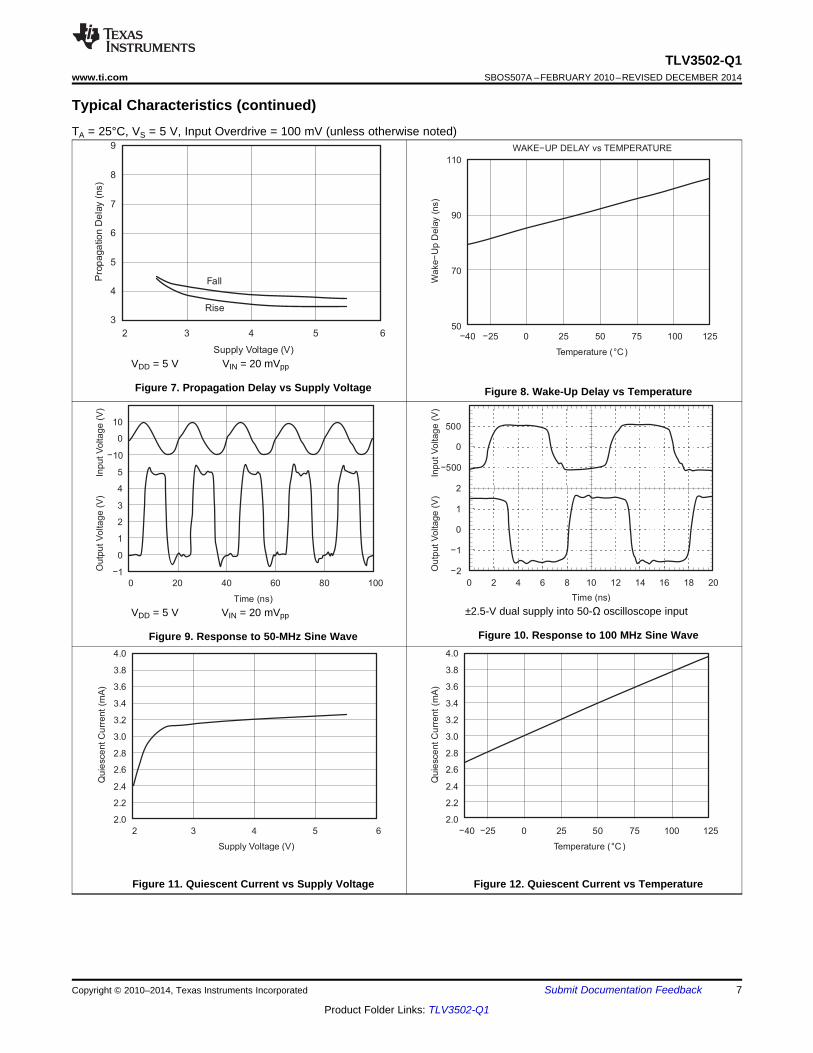
Typical Characteristics (continued)TA = 25°C, VS = 5 V, Input Overdrive = 100 mV (unless otherwise noted)
Figure 13. Quiescent Current vs Shutdown Voltage Figure 14. Quiescent Current vs Frequency
8 Submit Documentation Feedback Copyright © 2010–2014, Texas Instruments Incorporated
Product Folder Links: TLV3502-Q1
VIN
Vref
VOUT
VS
0.1 µF 2.2 µFR
+IN A
±IN A
+
±
A
V+
V±
+IN B
±IN B
+
±
B
V+
V±
OUT A
OUT B
TLV3502-Q1www.ti.com SBOS507A –FEBRUARY 2010–REVISED DECEMBER 2014
7 Detailed Description
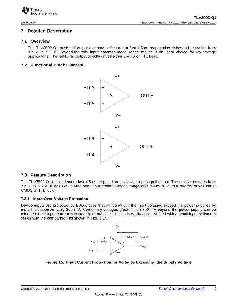
7.1 OverviewThe TLV3502-Q1 push-pull output comparator features a fast 4.5-ns propagation delay and operation from2.7 V to 5.5 V. Beyond-the-rails input common-mode range makes it an ideal choice for low-voltageapplications. The rail-to-rail output directly drives either CMOS or TTL logic.
7.2 Functional Block Diagram
7.3 Feature DescriptionThe TLV3502-Q1 device feature fast 4.5-ns propagation delay with a push-pull output. The device operates from2.7 V to 5.5 V. It has beyond-the-rails input common-mode range and rail-to-rail output directly drives eitherCMOS or TTL logic.
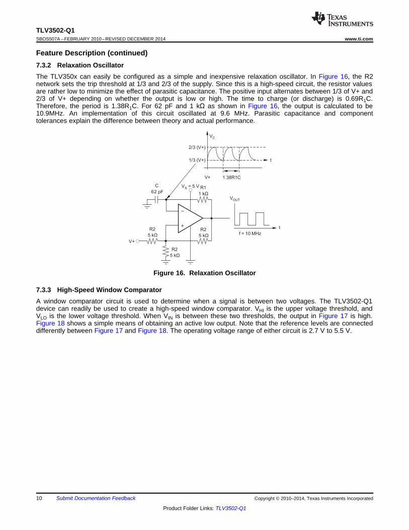
7.3.1 Input Over-Voltage ProtectionDevice inputs are protected by ESD diodes that will conduct if the input voltages exceed the power supplies bymore than approximately 300 mV. Momentary voltages greater than 300 mV beyond the power supply can betolerated if the input current is limited to 10 mA. This limiting is easily accomplished with a small input resistor inseries with the comparator, as shown in Figure 15.
Figure 15. Input Current Protection for Voltages Exceeding the Supply Voltage
Copyright © 2010–2014, Texas Instruments Incorporated Submit Documentation Feedback 9
Product Folder Links: TLV3502-Q1
V+
f = 10 MHz
VS = 5 V
2/3 (V+)
1/3 (V+)
R1
1 kΩ
R2
5 kΩ
VOUT
VC
V+
t
C
62 pF
1.38R1C
t
R2
5 kΩ
R2
5 kΩ
TLV3502-Q1SBOS507A –FEBRUARY 2010–REVISED DECEMBER 2014 www.ti.com
Feature Description (continued)7.3.2 Relaxation OscillatorThe TLV350x can easily be configured as a simple and inexpensive relaxation oscillator. In Figure 16, the R2network sets the trip threshold at 1/3 and 2/3 of the supply. Since this is a high-speed circuit, the resistor valuesare rather low to minimize the effect of parasitic capacitance. The positive input alternates between 1/3 of V+ and2/3 of V+ depending on whether the output is low or high. The time to charge (or discharge) is 0.69R1C.Therefore, the period is 1.38R1C. For 62 pF and 1 kΩ as shown in Figure 16, the output is calculated to be10.9MHz. An implementation of this circuit oscillated at 9.6 MHz. Parasitic capacitance and componenttolerances explain the difference between theory and actual performance.
Figure 16. Relaxation Oscillator
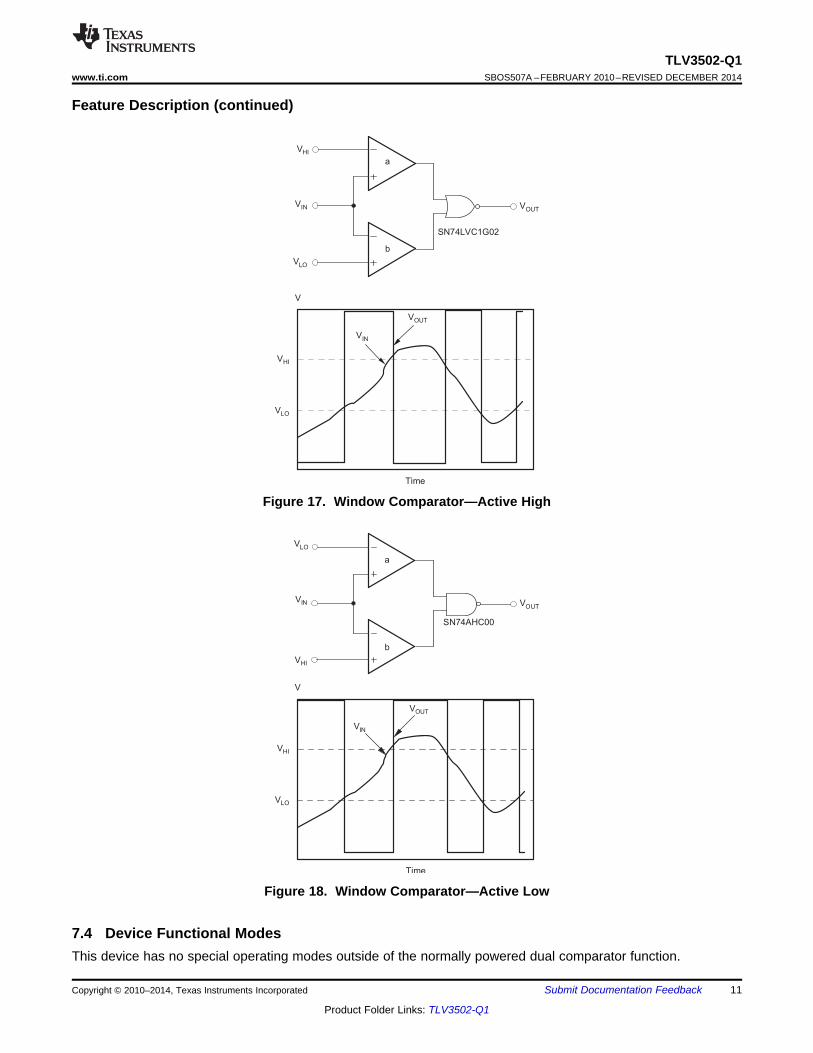
7.3.3 High-Speed Window ComparatorA window comparator circuit is used to determine when a signal is between two voltages. The TLV3502-Q1device can readily be used to create a high-speed window comparator. VHI is the upper voltage threshold, andVLO is the lower voltage threshold. When VIN is between these two thresholds, the output in Figure 17 is high.Figure 18 shows a simple means of obtaining an active low output. Note that the reference levels are connecteddifferently between Figure 17 and Figure 18. The operating voltage range of either circuit is 2.7 V to 5.5 V.
10 Submit Documentation Feedback Copyright © 2010–2014, Texas Instruments Incorporated
Product Folder Links: TLV3502-Q1
VOUT
VHI
VLO
VIN
SN74AHC00
VHI
VLO
VIN
VOUT
V
Time
a
b
a
VOUT
VHI
VLO
VIN
SN74LVC1G02
VHI
VLO
VIN
VOUT
V
Time
b
TLV3502-Q1www.ti.com SBOS507A –FEBRUARY 2010–REVISED DECEMBER 2014
Feature Description (continued)
Figure 17. Window Comparator—Active High
Figure 18. Window Comparator—Active Low
7.4 Device Functional ModesThis device has no special operating modes outside of the normally powered dual comparator function.
Copyright © 2010–2014, Texas Instruments Incorporated Submit Documentation Feedback 11
Product Folder Links: TLV3502-Q1
HYST
(V ) R1V 6 mV
R1 R2
+ ´= +
+
VIN
Vref
VOUT
VS = 5 V
0.1 µF 2.2 µF
R1= 51 Ω R2 = 10 kΩ
TLV3502-Q1SBOS507A –FEBRUARY 2010–REVISED DECEMBER 2014 www.ti.com
8 Application and Implementation
NOTEInformation in the following applications sections is not part of the TI componentspecification, and TI does not warrant its accuracy or completeness. TI’s customers areresponsible for determining suitability of components for their purposes. Customers shouldvalidate and test their design implementation to confirm system functionality.
8.1 Application InformationThe TLV3502-Q1 device features high-speed response and includes 6 mV of internal hysteresis for improvednoise immunity with an input common-mode range that extends 0.2 V beyond the power-supply rails.
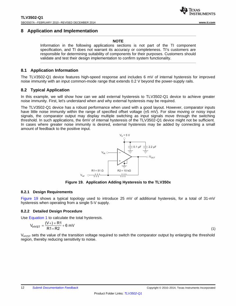
8.2 Typical ApplicationIn this example, we will show how can we add external hysteresis to TLV3502-Q1 device to achieve greaternoise immunity. First, let's understand when and why external hysteresis may be required.
The TLV3502-Q1 device has a robust performance when used with a good layout. However, comparator inputshave little noise immunity within the range of specified offset voltage (±5 mV). For slow moving or noisy inputsignals, the comparator output may display multiple switching as input signals move through the switchingthreshold. In such applications, the 6mV of internal hysteresis of the TLV3502-Q1 device might not be sufficient.In cases where greater noise immunity is desired, external hysteresis may be added by connecting a smallamount of feedback to the positive input.
Figure 19. Application Adding Hysteresis to the TLV350x
8.2.1 Design RequirementsFigure 19 shows a typical topology used to introduce 25 mV of additional hysteresis, for a total of 31-mVhysteresis when operating from a single 5-V supply.
8.2.2 Detailed Design ProcedureUse Equation 1 to calculate the total hysteresis.
(1)
VHYST sets the value of the transition voltage required to switch the comparator output by enlarging the thresholdregion, thereby reducing sensitivity to noise.
12 Submit Documentation Feedback Copyright © 2010–2014, Texas Instruments Incorporated
Product Folder Links: TLV3502-Q1
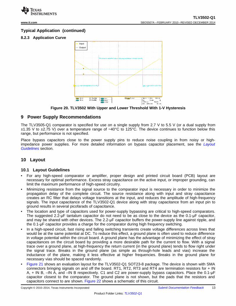
Input
Output
TLV3502-Q1www.ti.com SBOS507A –FEBRUARY 2010–REVISED DECEMBER 2014
Typical Application (continued)8.2.3 Application Curve
Figure 20. TLV3502 With Upper and Lower Threshold With 1-V Hysteresis
9 Power Supply RecommendationsThe TLV3505-Q1 comparator is specified for use on a single supply from 2.7 V to 5.5 V (or a dual supply from±1.35 V to ±2.75 V) over a temperature range of −40°C to 125°C. The device continues to function below thisrange, but performance is not specified.
Place bypass capacitors close to the power supply pins to reduce noise coupling in from noisy or high-impedance power supplies. For more detailed information on bypass capacitor placement, see the LayoutGuidelines section.
10 Layout
10.1 Layout Guidelines• For any high-speed comparator or amplifier, proper design and printed circuit board (PCB) layout are
necessary for optimal performance. Excess stray capacitance on the active input, or improper grounding, canlimit the maximum performance of high-speed circuitry.
• Minimizing resistance from the signal source to the comparator input is necessary in order to minimize thepropagation delay of the complete circuit. The source resistance along with input and stray capacitancecreates an RC filter that delays voltage transitions at the input, and reduces the amplitude of high-frequencysignals. The input capacitance of the TLV3502-Q1 device along with stray capacitance from an input pin toground results in several picofarads of capacitance.
• The location and type of capacitors used for power-supply bypassing are critical to high-speed comparators.The suggested 2.2-μF tantalum capacitor do not need to be as close to the device as the 0.1-μF capacitor,and may be shared with other devices. The 2.2-μF capacitor buffers the power-supply line against ripple, andthe 0.1-μF capacitor provides a charge for the comparator during high frequency switching.
• In a high-speed circuit, fast rising and falling switching transients create voltage differences across lines thatwould be at the same potential at DC. To reduce this effect, a ground plane is often used to reduce differencein voltage potential within the circuit board. A ground plane has the advantage of minimizing the effect of straycapacitances on the circuit board by providing a more desirable path for the current to flow. With a signaltrace over a ground plane, at high-frequency the return current (in the ground plane) tends to flow right underthe signal trace. Breaks in the ground plane (as simple as through-hole leads and vias) increase theinductance of the plane, making it less effective at higher frequencies. Breaks in the ground plane fornecessary vias should be spaced randomly.
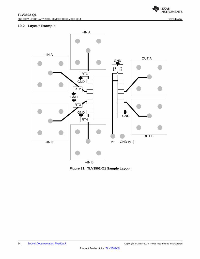
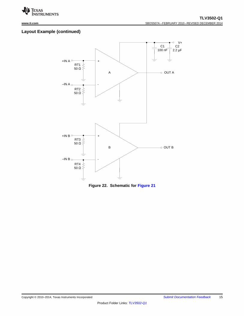
• Figure 21 shows an evaluation layout for the TLV3502-Q1 SOT23-8 package. The device is shown with SMAconnectors bringing signals on and off the board. RT1, RT2, RT3 and RT4 are termination resistors for + INA, + IN B, –IN A, and –IN B respectively. C1 and C2 are power-supply bypass capacitors. Place the 0.1-μFcapacitor closest to the comparator. The ground plane is not shown, but the pads that the resistors andcapacitors connect to are shown. Figure 22 shows a schematic of this circuit.
Copyright © 2010–2014, Texas Instruments Incorporated Submit Documentation Feedback 13
Product Folder Links: TLV3502-Q1
+IN A
GND
GNDOUT A
OUT B
±IN A
+IN B
±IN B
GND (V±)V+
C1
C2
RT1
RT2
RT4
RT3
GND
GND
GND
TLV3502-Q1SBOS507A –FEBRUARY 2010–REVISED DECEMBER 2014 www.ti.com
10.2 Layout Example
Figure 21. TLV3502-Q1 Sample Layout
14 Submit Documentation Feedback Copyright © 2010–2014, Texas Instruments Incorporated
Product Folder Links: TLV3502-Q1
+IN A
±IN A
+
-
A
V+
+IN B
±IN B
+
-
B
OUT A
OUT B
C1100 nF
C22.2 µF
RT150 �
RT250 �
RT350 �
RT450 �
TLV3502-Q1www.ti.com SBOS507A –FEBRUARY 2010–REVISED DECEMBER 2014
Layout Example (continued)
Figure 22. Schematic for Figure 21
Copyright © 2010–2014, Texas Instruments Incorporated Submit Documentation Feedback 15
Product Folder Links: TLV3502-Q1
TLV3502-Q1SBOS507A –FEBRUARY 2010–REVISED DECEMBER 2014 www.ti.com
11 Device and Documentation Support
11.1 TrademarksAll trademarks are the property of their respective owners.
11.2 Electrostatic Discharge CautionThese devices have limited built-in ESD protection. The leads should be shorted together or the device placed in conductive foamduring storage or handling to prevent electrostatic damage to the MOS gates.
11.3 GlossarySLYZ022 — TI Glossary.
This glossary lists and explains terms, acronyms, and definitions.
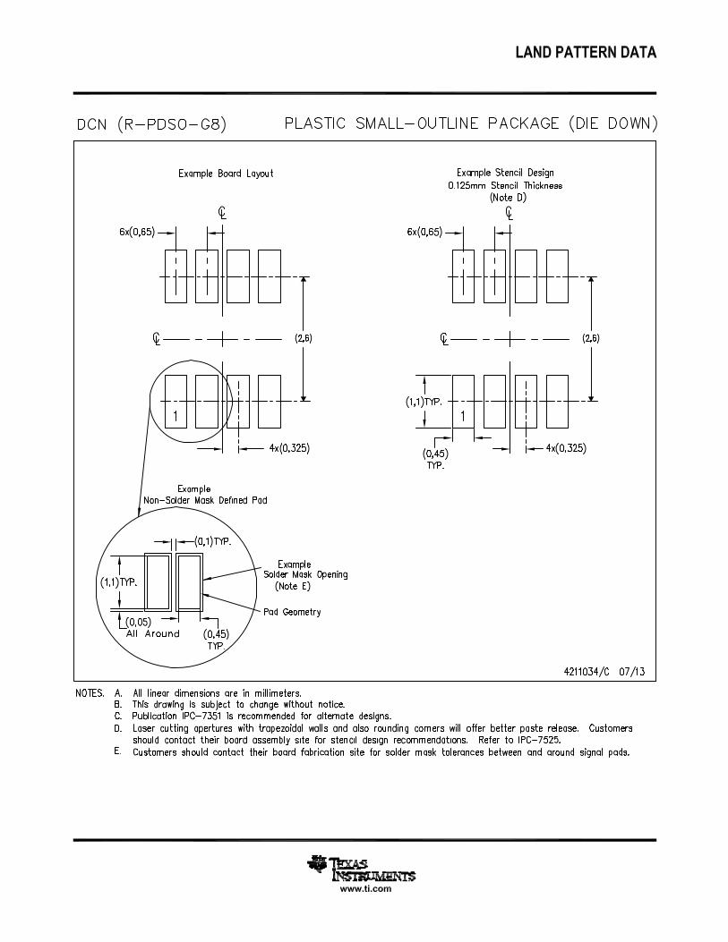
12 Mechanical, Packaging, and Orderable InformationThe following pages include mechanical, packaging, and orderable information. This information is the mostcurrent data available for the designated devices. This data is subject to change without notice and revision ofthis document. For browser-based versions of this data sheet, refer to the left-hand navigation.
16 Submit Documentation Feedback Copyright © 2010–2014, Texas Instruments Incorporated
Product Folder Links: TLV3502-Q1
PACKAGE OPTION ADDENDUM
www.ti.com 23-Jun-2014
Addendum-Page 1
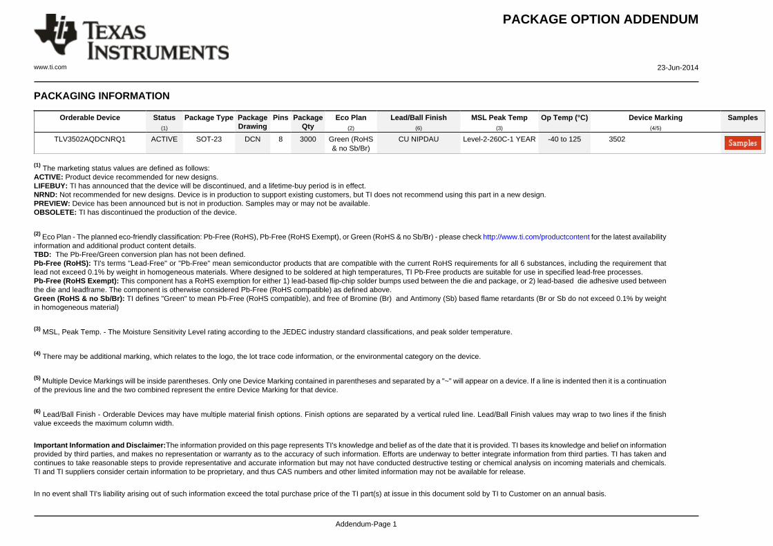
PACKAGING INFORMATION
Orderable Device Status(1)
Package Type PackageDrawing
Pins PackageQty
Eco Plan(2)
Lead/Ball Finish(6)
MSL Peak Temp(3)
Op Temp (°C) Device Marking(4/5)
Samples
TLV3502AQDCNRQ1 ACTIVE SOT-23 DCN 8 3000 Green (RoHS& no Sb/Br)
CU NIPDAU Level-2-260C-1 YEAR -40 to 125 3502
(1) The marketing status values are defined as follows:ACTIVE: Product device recommended for new designs.LIFEBUY: TI has announced that the device will be discontinued, and a lifetime-buy period is in effect.NRND: Not recommended for new designs. Device is in production to support existing customers, but TI does not recommend using this part in a new design.PREVIEW: Device has been announced but is not in production. Samples may or may not be available.OBSOLETE: TI has discontinued the production of the device.
(2) Eco Plan - The planned eco-friendly classification: Pb-Free (RoHS), Pb-Free (RoHS Exempt), or Green (RoHS & no Sb/Br) - please check http://www.ti.com/productcontent for the latest availabilityinformation and additional product content details.TBD: The Pb-Free/Green conversion plan has not been defined.Pb-Free (RoHS): TI's terms "Lead-Free" or "Pb-Free" mean semiconductor products that are compatible with the current RoHS requirements for all 6 substances, including the requirement thatlead not exceed 0.1% by weight in homogeneous materials. Where designed to be soldered at high temperatures, TI Pb-Free products are suitable for use in specified lead-free processes.Pb-Free (RoHS Exempt): This component has a RoHS exemption for either 1) lead-based flip-chip solder bumps used between the die and package, or 2) lead-based die adhesive used betweenthe die and leadframe. The component is otherwise considered Pb-Free (RoHS compatible) as defined above.Green (RoHS & no Sb/Br): TI defines "Green" to mean Pb-Free (RoHS compatible), and free of Bromine (Br) and Antimony (Sb) based flame retardants (Br or Sb do not exceed 0.1% by weightin homogeneous material)
(3) MSL, Peak Temp. - The Moisture Sensitivity Level rating according to the JEDEC industry standard classifications, and peak solder temperature.
(4) There may be additional marking, which relates to the logo, the lot trace code information, or the environmental category on the device.
(5) Multiple Device Markings will be inside parentheses. Only one Device Marking contained in parentheses and separated by a "~" will appear on a device. If a line is indented then it is a continuationof the previous line and the two combined represent the entire Device Marking for that device.
(6) Lead/Ball Finish - Orderable Devices may have multiple material finish options. Finish options are separated by a vertical ruled line. Lead/Ball Finish values may wrap to two lines if the finishvalue exceeds the maximum column width.
Important Information and Disclaimer:The information provided on this page represents TI's knowledge and belief as of the date that it is provided. TI bases its knowledge and belief on informationprovided by third parties, and makes no representation or warranty as to the accuracy of such information. Efforts are underway to better integrate information from third parties. TI has taken andcontinues to take reasonable steps to provide representative and accurate information but may not have conducted destructive testing or chemical analysis on incoming materials and chemicals.TI and TI suppliers consider certain information to be proprietary, and thus CAS numbers and other limited information may not be available for release.
In no event shall TI's liability arising out of such information exceed the total purchase price of the TI part(s) at issue in this document sold by TI to Customer on an annual basis.
PACKAGE OPTION ADDENDUM
www.ti.com 23-Jun-2014
Addendum-Page 2
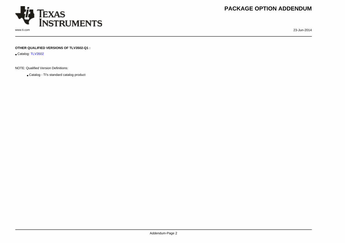
OTHER QUALIFIED VERSIONS OF TLV3502-Q1 :
• Catalog: TLV3502
NOTE: Qualified Version Definitions:
• Catalog - TI's standard catalog product
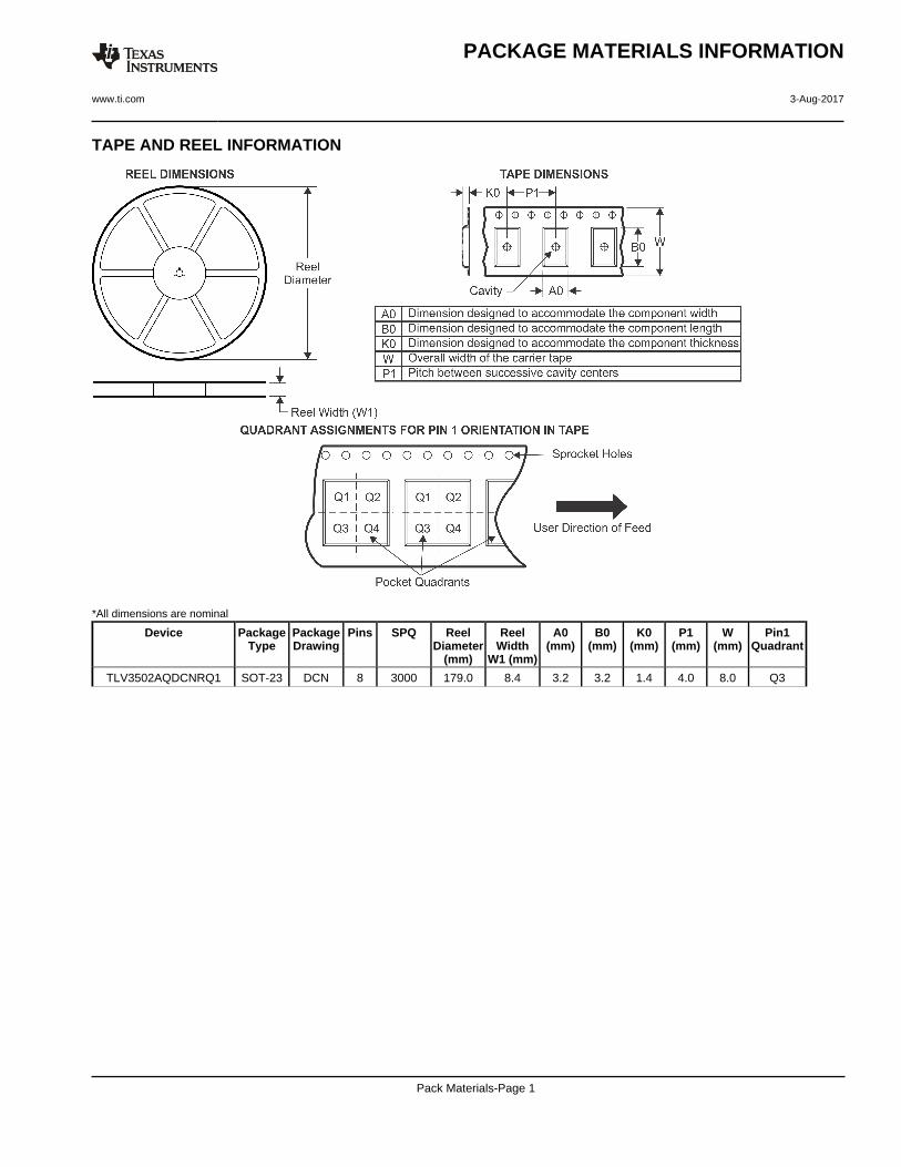
TAPE AND REEL INFORMATION
*All dimensions are nominal
Device PackageType
PackageDrawing
Pins SPQ ReelDiameter
(mm)
ReelWidth
W1 (mm)
A0(mm)
B0(mm)
K0(mm)
P1(mm)
W(mm)
Pin1Quadrant
TLV3502AQDCNRQ1 SOT-23 DCN 8 3000 179.0 8.4 3.2 3.2 1.4 4.0 8.0 Q3
PACKAGE MATERIALS INFORMATION
www.ti.com 3-Aug-2017
Pack Materials-Page 1
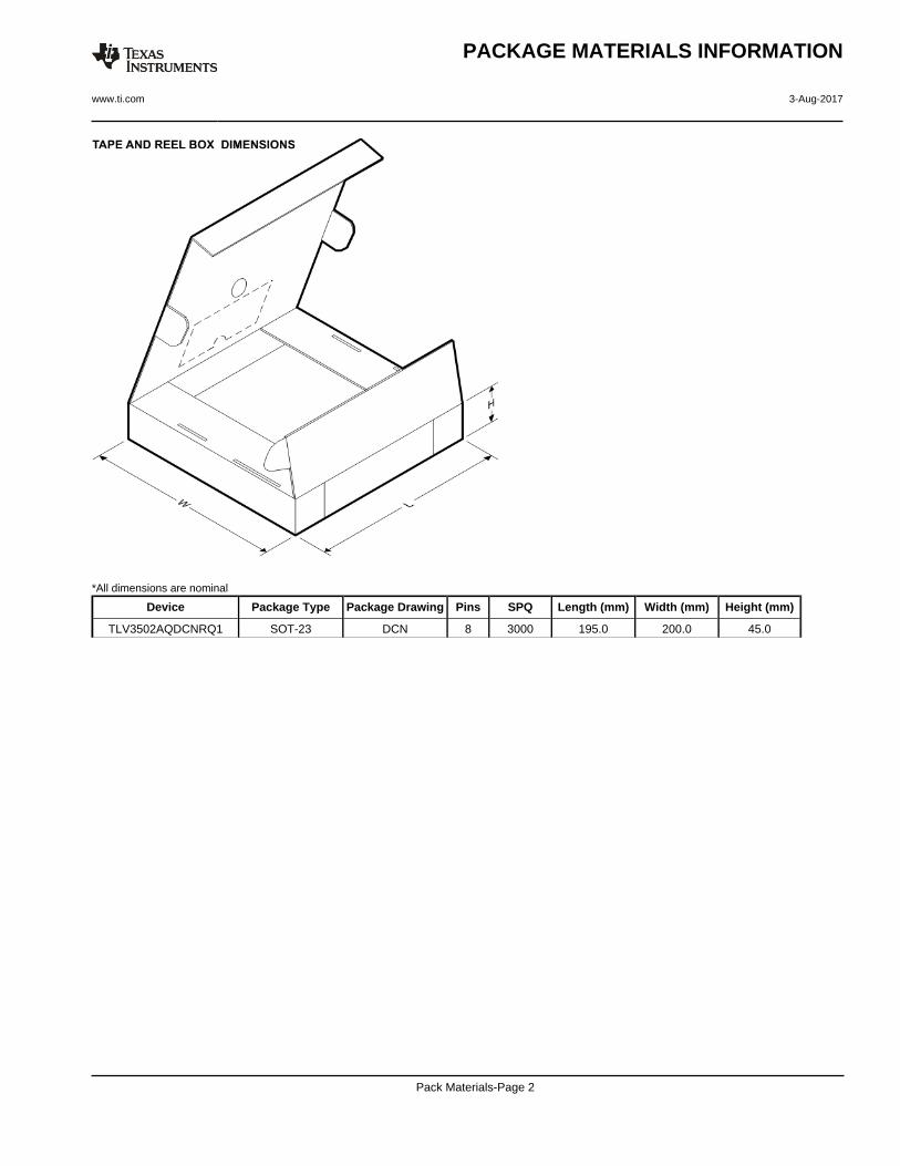
*All dimensions are nominal
Device Package Type Package Drawing Pins SPQ Length (mm) Width (mm) Height (mm)
TLV3502AQDCNRQ1 SOT-23 DCN 8 3000 195.0 200.0 45.0
PACKAGE MATERIALS INFORMATION
www.ti.com 3-Aug-2017
Pack Materials-Page 2

IMPORTANT NOTICE
Texas Instruments Incorporated (TI) reserves the right to make corrections, enhancements, improvements and other changes to itssemiconductor products and services per JESD46, latest issue, and to discontinue any product or service per JESD48, latest issue. Buyersshould obtain the latest relevant information before placing orders and should verify that such information is current and complete.TI’s published terms of sale for semiconductor products (http://www.ti.com/sc/docs/stdterms.htm) apply to the sale of packaged integratedcircuit products that TI has qualified and released to market. Additional terms may apply to the use or sale of other types of TI products andservices.Reproduction of significant portions of TI information in TI data sheets is permissible only if reproduction is without alteration and isaccompanied by all associated warranties, conditions, limitations, and notices. TI is not responsible or liable for such reproduceddocumentation. Information of third parties may be subject to additional restrictions. Resale of TI products or services with statementsdifferent from or beyond the parameters stated by TI for that product or service voids all express and any implied warranties for theassociated TI product or service and is an unfair and deceptive business practice. TI is not responsible or liable for any such statements.Buyers and others who are developing systems that incorporate TI products (collectively, “Designers”) understand and agree that Designersremain responsible for using their independent analysis, evaluation and judgment in designing their applications and that Designers havefull and exclusive responsibility to assure the safety of Designers' applications and compliance of their applications (and of all TI productsused in or for Designers’ applications) with all applicable regulations, laws and other applicable requirements. Designer represents that, withrespect to their applications, Designer has all the necessary expertise to create and implement safeguards that (1) anticipate dangerousconsequences of failures, (2) monitor failures and their consequences, and (3) lessen the likelihood of failures that might cause harm andtake appropriate actions. Designer agrees that prior to using or distributing any applications that include TI products, Designer willthoroughly test such applications and the functionality of such TI products as used in such applications.TI’s provision of technical, application or other design advice, quality characterization, reliability data or other services or information,including, but not limited to, reference designs and materials relating to evaluation modules, (collectively, “TI Resources”) are intended toassist designers who are developing applications that incorporate TI products; by downloading, accessing or using TI Resources in anyway, Designer (individually or, if Designer is acting on behalf of a company, Designer’s company) agrees to use any particular TI Resourcesolely for this purpose and subject to the terms of this Notice.TI’s provision of TI Resources does not expand or otherwise alter TI’s applicable published warranties or warranty disclaimers for TIproducts, and no additional obligations or liabilities arise from TI providing such TI Resources. TI reserves the right to make corrections,enhancements, improvements and other changes to its TI Resources. TI has not conducted any testing other than that specificallydescribed in the published documentation for a particular TI Resource.Designer is authorized to use, copy and modify any individual TI Resource only in connection with the development of applications thatinclude the TI product(s) identified in such TI Resource. NO OTHER LICENSE, EXPRESS OR IMPLIED, BY ESTOPPEL OR OTHERWISETO ANY OTHER TI INTELLECTUAL PROPERTY RIGHT, AND NO LICENSE TO ANY TECHNOLOGY OR INTELLECTUAL PROPERTYRIGHT OF TI OR ANY THIRD PARTY IS GRANTED HEREIN, including but not limited to any patent right, copyright, mask work right, orother intellectual property right relating to any combination, machine, or process in which TI products or services are used. Informationregarding or referencing third-party products or services does not constitute a license to use such products or services, or a warranty orendorsement thereof. Use of TI Resources may require a license from a third party under the patents or other intellectual property of thethird party, or a license from TI under the patents or other intellectual property of TI.TI RESOURCES ARE PROVIDED “AS IS” AND WITH ALL FAULTS. TI DISCLAIMS ALL OTHER WARRANTIES ORREPRESENTATIONS, EXPRESS OR IMPLIED, REGARDING RESOURCES OR USE THEREOF, INCLUDING BUT NOT LIMITED TOACCURACY OR COMPLETENESS, TITLE, ANY EPIDEMIC FAILURE WARRANTY AND ANY IMPLIED WARRANTIES OFMERCHANTABILITY, FITNESS FOR A PARTICULAR PURPOSE, AND NON-INFRINGEMENT OF ANY THIRD PARTY INTELLECTUALPROPERTY RIGHTS. TI SHALL NOT BE LIABLE FOR AND SHALL NOT DEFEND OR INDEMNIFY DESIGNER AGAINST ANY CLAIM,INCLUDING BUT NOT LIMITED TO ANY INFRINGEMENT CLAIM THAT RELATES TO OR IS BASED ON ANY COMBINATION OFPRODUCTS EVEN IF DESCRIBED IN TI RESOURCES OR OTHERWISE. IN NO EVENT SHALL TI BE LIABLE FOR ANY ACTUAL,DIRECT, SPECIAL, COLLATERAL, INDIRECT, PUNITIVE, INCIDENTAL, CONSEQUENTIAL OR EXEMPLARY DAMAGES INCONNECTION WITH OR ARISING OUT OF TI RESOURCES OR USE THEREOF, AND REGARDLESS OF WHETHER TI HAS BEENADVISED OF THE POSSIBILITY OF SUCH DAMAGES.Unless TI has explicitly designated an individual product as meeting the requirements of a particular industry standard (e.g., ISO/TS 16949and ISO 26262), TI is not responsible for any failure to meet such industry standard requirements.Where TI specifically promotes products as facilitating functional safety or as compliant with industry functional safety standards, suchproducts are intended to help enable customers to design and create their own applications that meet applicable functional safety standardsand requirements. Using products in an application does not by itself establish any safety features in the application. Designers mustensure compliance with safety-related requirements and standards applicable to their applications. Designer may not use any TI products inlife-critical medical equipment unless authorized officers of the parties have executed a special contract specifically governing such use.Life-critical medical equipment is medical equipment where failure of such equipment would cause serious bodily injury or death (e.g., lifesupport, pacemakers, defibrillators, heart pumps, neurostimulators, and implantables). Such equipment includes, without limitation, allmedical devices identified by the U.S. Food and Drug Administration as Class III devices and equivalent classifications outside the U.S.TI may expressly designate certain products as completing a particular qualification (e.g., Q100, Military Grade, or Enhanced Product).Designers agree that it has the necessary expertise to select the product with the appropriate qualification designation for their applicationsand that proper product selection is at Designers’ own risk. Designers are solely responsible for compliance with all legal and regulatoryrequirements in connection with such selection.Designer will fully indemnify TI and its representatives against any damages, costs, losses, and/or liabilities arising out of Designer’s non-compliance with the terms and provisions of this Notice.
Mailing Address: Texas Instruments, Post Office Box 655303, Dallas, Texas 75265Copyright © 2017, Texas Instruments Incorporated