Embed Size (px)
Citation preview
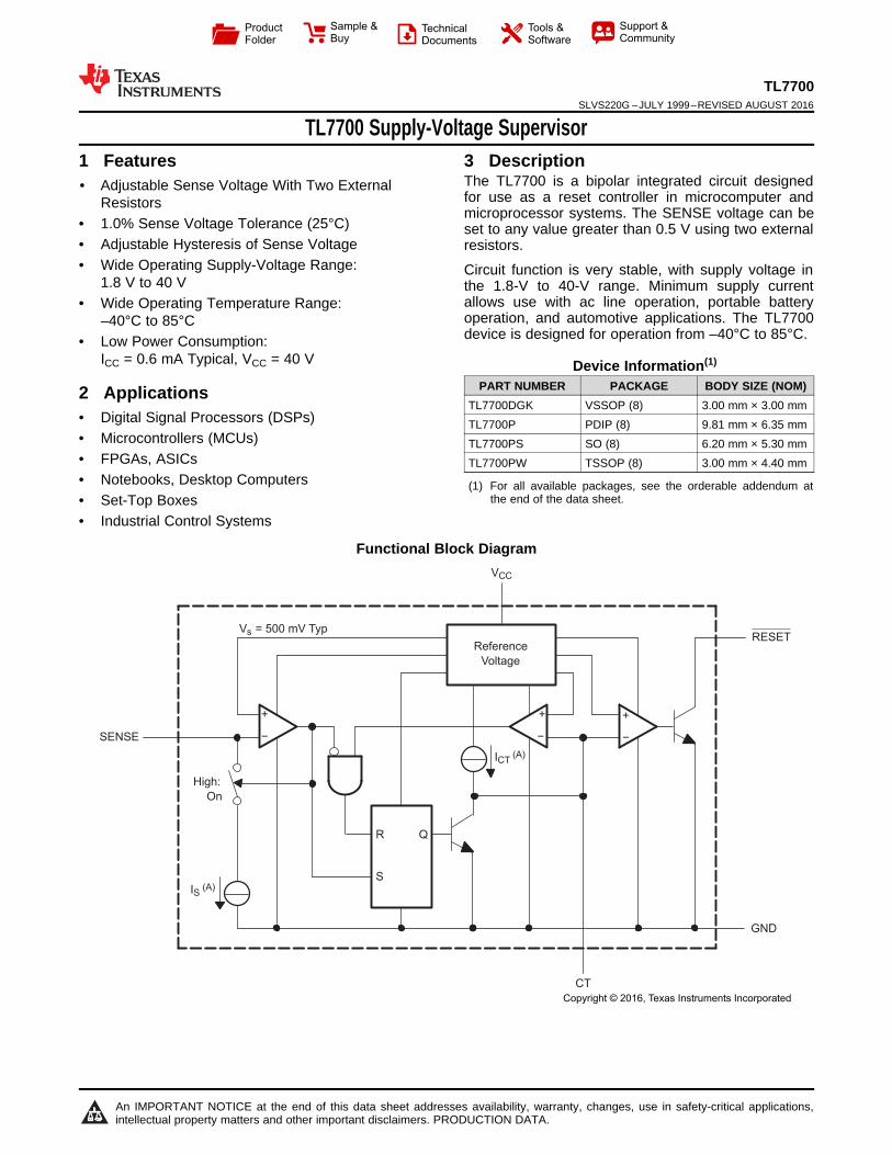
Reference
Voltage
+
−
+
−
R
S
Q
+
−
Vs = 500 mV TypRESET
GND
CT
SENSE
VCC
ICT(A)
High:
On
IS(A)
Copyright © 2016, Texas Instruments Incorporated
Product
Folder
Sample &Buy
Technical
Documents
Tools &
Software
Support &Community
An IMPORTANT NOTICE at the end of this data sheet addresses availability, warranty, changes, use in safety-critical applications,intellectual property matters and other important disclaimers. PRODUCTION DATA.
TL7700SLVS220G –JULY 1999–REVISED AUGUST 2016
TL7700 Supply-Voltage Supervisor
1
1 Features1• Adjustable Sense Voltage With Two External
Resistors• 1.0% Sense Voltage Tolerance (25°C)• Adjustable Hysteresis of Sense Voltage• Wide Operating Supply-Voltage Range:
1.8 V to 40 V• Wide Operating Temperature Range:
–40°C to 85°C• Low Power Consumption:
ICC = 0.6 mA Typical, VCC = 40 V
2 Applications• Digital Signal Processors (DSPs)• Microcontrollers (MCUs)• FPGAs, ASICs• Notebooks, Desktop Computers• Set-Top Boxes• Industrial Control Systems
3 DescriptionThe TL7700 is a bipolar integrated circuit designedfor use as a reset controller in microcomputer andmicroprocessor systems. The SENSE voltage can beset to any value greater than 0.5 V using two externalresistors.
Circuit function is very stable, with supply voltage inthe 1.8-V to 40-V range. Minimum supply currentallows use with ac line operation, portable batteryoperation, and automotive applications. The TL7700device is designed for operation from –40°C to 85°C.
Device Information(1)
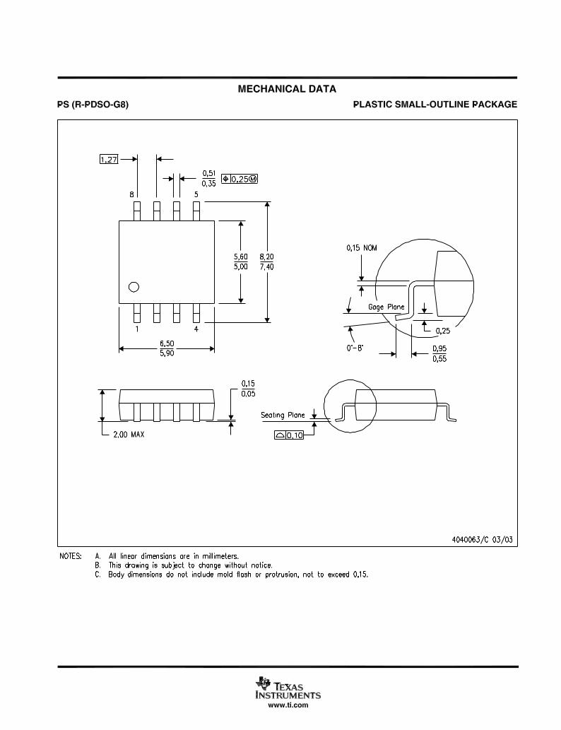
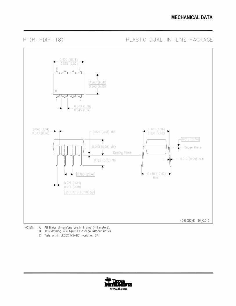
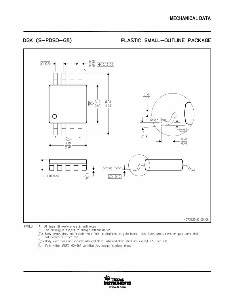
PART NUMBER PACKAGE BODY SIZE (NOM)TL7700DGK VSSOP (8) 3.00 mm × 3.00 mmTL7700P PDIP (8) 9.81 mm × 6.35 mmTL7700PS SO (8) 6.20 mm × 5.30 mmTL7700PW TSSOP (8) 3.00 mm × 4.40 mm
(1) For all available packages, see the orderable addendum atthe end of the data sheet.
Functional Block Diagram
2
TL7700SLVS220G –JULY 1999–REVISED AUGUST 2016 www.ti.com
Product Folder Links: TL7700
Submit Documentation Feedback Copyright © 1999–2016, Texas Instruments Incorporated
Table of Contents1 Features .................................................................. 12 Applications ........................................................... 13 Description ............................................................. 14 Revision History..................................................... 25 Pin Configuration and Functions ......................... 36 Specifications......................................................... 4
6.1 Absolute Maximum Ratings ...................................... 46.2 ESD Ratings.............................................................. 46.3 Recommended Operating Conditions....................... 46.4 Thermal Information .................................................. 46.5 Electrical Characteristics........................................... 56.6 Switching Characteristics .......................................... 56.7 Typical Characteristics .............................................. 6
7 Parameter Measurement Information .................. 88 Detailed Description ............................................ 10
8.1 Overview ................................................................. 108.2 Functional Block Diagram ....................................... 10
8.3 Feature Description................................................. 108.4 Device Functional Modes........................................ 12
9 Application and Implementation ........................ 139.1 Application Information............................................ 139.2 Typical Application ................................................. 13
10 Power Supply Recommendations ..................... 1511 Layout................................................................... 15
11.1 Layout Guidelines ................................................. 1511.2 Layout Example .................................................... 15
12 Device and Documentation Support ................. 1612.1 Receiving Notification of Documentation Updates 1612.2 Community Resource............................................ 1612.3 Trademarks ........................................................... 1612.4 Electrostatic Discharge Caution............................ 1612.5 Glossary ................................................................ 16
13 Mechanical, Packaging, and OrderableInformation ........................................................... 16
4 Revision HistoryNOTE: Page numbers for previous revisions may differ from page numbers in the current version.
Changes from Revision F (August 2011) to Revision G Page
• Added ESD Ratings table, Feature Description section, Device Functional Modes, Application and Implementationsection, Power Supply Recommendations section, Layout section, Device and Documentation Support section, andMechanical, Packaging, and Orderable Information section ................................................................................................. 1
• Deleted Ordering Information table, see POA at the end of the data sheet........................................................................... 1• Changed values in the Thermal Information table to align with JEDEC standards................................................................ 4
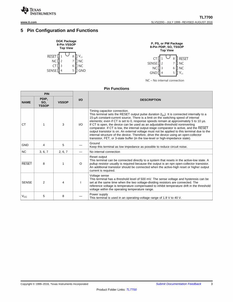
1
2
3
4
8
7
6
5
CT
SENSE
NC
GND
RESET
NC
NC
VCC
NC – No internal connection
1
2
3
4
8
7
6
5
RESET
NC
CT
SENSE
VCC
NC
NC
GND
3
TL7700www.ti.com SLVS220G –JULY 1999–REVISED AUGUST 2016
Product Folder Links: TL7700
Submit Documentation FeedbackCopyright © 1999–2016, Texas Instruments Incorporated
5 Pin Configuration and Functions
DGK Package8-Pin VSSOP
Top ViewP, PS, or PW Package
8-Pin PDIP, SO, TSSOPTop View
Pin FunctionsPIN
I/O DESCRIPTIONNAME
PDIP,SO,
TSSOPVSSOP
CT 1 3 I/O
Timing capacitor connection.This terminal sets the RESET output pulse duration (tpo). It is connected internally to a15-µA constant-current source. There is a limit on the switching speed of internalelements; even if CT is set to 0, response speeds remain at approximately 5 to 10 µs.If CT is open, the device can be used as an adjustable-threshold noninvertingcomparator. If CT is low, the internal output-stage comparator is active, and the RESEToutput transistor is on. An external voltage must not be applied to this terminal due to theinternal structure of the device. Therefore, drive the device using an open-collectortransistor, FET, or 3-state buffer (in the low-level or high-impedance state).
GND 4 5 — GroundKeep this terminal as low impedance as possible to reduce circuit noise.
NC 3, 6, 7 2, 6, 7 — No internal connection
RESET 8 1 O
Reset outputThis terminal can be connected directly to a system that resets in the active-low state. Apullup resistor usually is required because the output is an npn open-collector transistor.An additional transistor should be connected when the active-high reset or higher outputcurrent is required.
SENSE 2 4 I
Voltage senseThis terminal has a threshold level of 500 mV. The sense voltage and hysteresis can beset at the same time when the two voltage-dividing resistors are connected. Thereference voltage is temperature compensated to inhibit temperature drift in the thresholdvoltage within the operating temperature range.
VCC 5 8 — Power supplyThis terminal is used in an operating-voltage range of 1.8 V to 40 V.
4
TL7700SLVS220G –JULY 1999–REVISED AUGUST 2016 www.ti.com
Product Folder Links: TL7700
Submit Documentation Feedback Copyright © 1999–2016, Texas Instruments Incorporated
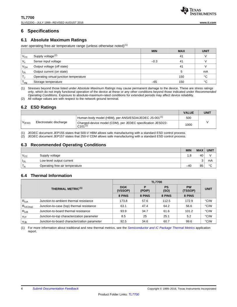
(1) Stresses beyond those listed under Absolute Maximum Ratings may cause permanent damage to the device. These are stress ratingsonly, which do not imply functional operation of the device at these or any other conditions beyond those indicated under RecommendedOperating Conditions. Exposure to absolute-maximum-rated conditions for extended periods may affect device reliability.
(2) All voltage values are with respect to the network ground terminal.
6 Specifications
6.1 Absolute Maximum Ratingsover operating free-air temperature range (unless otherwise noted) (1)
MIN MAX UNITVCC Supply voltage (2) 41 VVs Sense input voltage –0.3 41 VVOH Output voltage (off state) 41 VIOL Output current (on state) 5 mATJ Operating virtual-junction temperature 150 °CTstg Storage temperature –65 150 °C
(1) JEDEC document JEP155 states that 500-V HBM allows safe manufacturing with a standard ESD control process.(2) JEDEC document JEP157 states that 250-V CDM allows safe manufacturing with a standard ESD control process.
6.2 ESD RatingsVALUE UNIT
V(ESD) Electrostatic dischargeHuman-body model (HBM), per ANSI/ESDA/JEDEC JS-001 (1) 500
VCharged-device model (CDM), per JEDEC specification JESD22-C101 (2) 1000
6.3 Recommended Operating ConditionsMIN MAX UNIT
VCC Supply voltage 1.8 40 VIOL Low-level output current 3 mATA Operating free-air temperature –40 85 °C
(1) For more information about traditional and new thermal metrics, see the Semiconductor and IC Package Thermal Metrics applicationreport.
6.4 Thermal Information
THERMAL METRIC (1)
TL7700
UNITDGK(VSSOP)
P(PDIP)
PS(SO)
PW(TSSOP)
8 PINS 8 PINS 8 PINS 8 PINSRθJA Junction-to-ambient thermal resistance 173.8 57.6 112.5 172.9 °C/WRθJC(top) Junction-to-case (top) thermal resistance 63.1 47.4 64.2 56.6 °C/WRθJB Junction-to-board thermal resistance 93.9 34.7 61.6 101.2 °C/WψJT Junction-to-top characterization parameter 8.5 25 25.1 5.2 °C/WψJB Junction-to-board characterization parameter 92.5 34.6 60.7 99.6 °C/W
5
TL7700www.ti.com SLVS220G –JULY 1999–REVISED AUGUST 2016
Product Folder Links: TL7700
Submit Documentation FeedbackCopyright © 1999–2016, Texas Instruments Incorporated
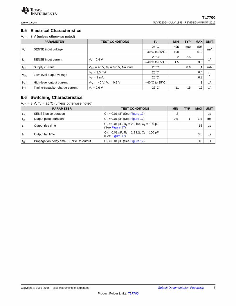
6.5 Electrical CharacteristicsVCC = 3 V (unless otherwise noted)
PARAMETER TEST CONDITIONS TA MIN TYP MAX UNIT
Vs SENSE input voltage25°C 495 500 505
mV–40°C to 85°C 490 510
Is SENSE input current Vs = 0.4 V25°C 2 2.5 3
µA–40°C to 85°C 1.5 3.5
ICC Supply current VCC = 40 V, Vs = 0.6 V, No load 25°C 0.6 1 mA
VOL Low-level output voltageIOL = 1.5 mA 25°C 0.4
VIOL = 3 mA 25°C 0.8
IOH High-level output current VOH = 40 V, Vs = 0.6 V –40°C to 85°C 1 µAICT Timing-capacitor charge current Vs = 0.6 V 25°C 11 15 19 µA
6.6 Switching CharacteristicsVCC = 3 V, TA = 25°C (unless otherwise noted)
PARAMETER TEST CONDITIONS MIN TYP MAX UNITtpi SENSE pulse duration CT = 0.01 µF (See Figure 17) 2 µstpo Output pulse duration CT = 0.01 µF (See Figure 17) 0.5 1 1.5 ms
tr Output rise time CT = 0.01 µF, RL = 2.2 kΩ, CL = 100 pF(See Figure 17) 15 µs
tf Output fall time CT = 0.01 µF, RL = 2.2 kΩ, CL = 100 pF(See Figure 17) 0.5 µs
tpd Propagation delay time, SENSE to output CT = 0.01 µF (See Figure 17) 10 µs
1
1
101
102
103
104
105
106
107
108
109
101 102 103 104 105 106 107 108 109
t po
−O
utp
ut
Pu
lse D
ura
tio
n−
ms
Ct − Timing Capacitor − pF
0−1.0
−0.5
0
0.5
1.0
1.5
2.0
2.5
3.0
3.5
0.1 0.2 0.3 0.4 0.5 0.6 1.0 10 40
Vs − Sense Input Voltage − V
I s−
Sen
se
In
pu
t C
urr
en
t−
mA
0 1 2 3 4 5 60
0.2
0.4
0.6
0.8
1.0
1.2
IOL − Low-Level Output Current − mA
VO
L−
Lo
w-L
evel
Ou
tpu
t Vo
ltag
e−
V
TA = 85°C
TA = 25°C
TA = −40°C
−75488
490
492
494
496
498
500
502
504
506
−50 −25 0 25 50 75 100 125 150
TA − Free-Air Temperature − °C
TA = 25°C
Vs = 500.8 mV
TA = 25°C
Vs = 498.3 mV
Vs
−S
en
se In
pu
t Vo
ltag
e−
mV
0 10 20 30 40 50 600
0.2
0.4
0.6
0.8
1.0
1.2
TA = 85°C
TA = 25°C
TA = −40°C
VCC − Supply Voltage − V
I CC
−S
up
ply
Cu
rren
t−
mA
0 10 20 30 40 50 6010
11
12
13
14
15
16
VCC − Supply Voltage − V
TA = 85°C
TA = 25°C
TA = −40°C
Tim
ing
-Cap
acit
or
Ch
arg
e C
urr
en
t−
mA
6
TL7700SLVS220G –JULY 1999–REVISED AUGUST 2016 www.ti.com
Product Folder Links: TL7700
Submit Documentation Feedback Copyright © 1999–2016, Texas Instruments Incorporated
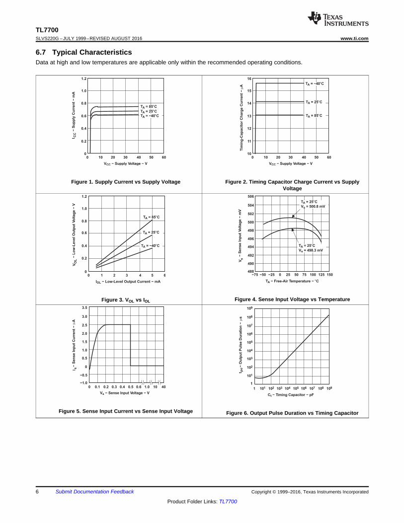
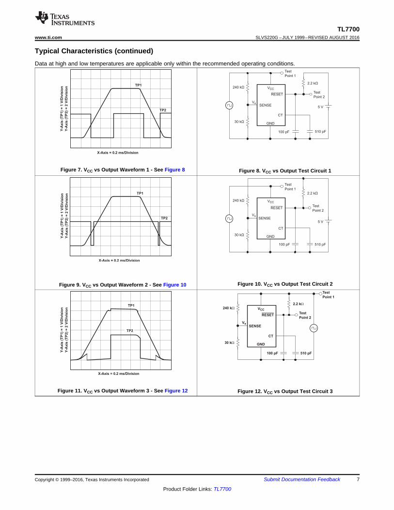
6.7 Typical CharacteristicsData at high and low temperatures are applicable only within the recommended operating conditions.
Figure 1. Supply Current vs Supply Voltage Figure 2. Timing Capacitor Charge Current vs SupplyVoltage
Figure 3. VOL vs IOL Figure 4. Sense Input Voltage vs Temperature
Figure 5. Sense Input Current vs Sense Input Voltage Figure 6. Output Pulse Duration vs Timing Capacitor
X-Axis = 0.2 ms/Division
TP1
TP2
Y-A
xis
(T
P1)
= 1
V/D
ivis
ion
Y-A
xis
(T
P2)
= 2
V/D
ivis
ion VCC
Vs
GND
CT
RESET
2.2 kW
30 kW
510 pF
Test
Point 1
240 kW
100 pF
Test
Point 2
SENSE
TP2
X-Axis = 0.2 ms/Division
TP1
Y-A
xis
(T
P1)
= 1
V/D
ivis
ion
Y-A
xis
(T
P2)
= 2
V/D
ivis
ion
VCC
Vs
GND
CT
RESET
2.2 kΩ
30 kΩ
510 pF
Test
Point 1
240 kΩ
100 pF
Test
Point 2
5 VSENSE
X-Axis = 0.2 ms/Division
TP1
TP2
Y-A
xis
(T
P1)
= 1
V/D
ivis
ion
Y-A
xis
(T
P2)
= 2
V/D
ivis
ion VCC
Vs
GND
CT
RESET
2.2 kΩ
30 kΩ
510 pF
Test
Point 1
240 kΩ
100 pF
Test
Point 2
5 VSENSE
7
TL7700www.ti.com SLVS220G –JULY 1999–REVISED AUGUST 2016
Product Folder Links: TL7700
Submit Documentation FeedbackCopyright © 1999–2016, Texas Instruments Incorporated
Typical Characteristics (continued)Data at high and low temperatures are applicable only within the recommended operating conditions.
Figure 7. VCC vs Output Waveform 1 - See Figure 8 Figure 8. VCC vs Output Test Circuit 1
Figure 9. VCC vs Output Waveform 2 - See Figure 10 Figure 10. VCC vs Output Test Circuit 2
Figure 11. VCC vs Output Waveform 3 - See Figure 12 Figure 12. VCC vs Output Test Circuit 3
0.4 V
VCC
Vs
GND
3 V
CT
RESET
0.01 mF
Test
Point
SENSE
VCC
VCC
Vs
GND0.6 V
CTSENSE
A
+
−
VCC
VCC
Vs
GND0.6 V
SENSE
A+−
8
TL7700SLVS220G –JULY 1999–REVISED AUGUST 2016 www.ti.com
Product Folder Links: TL7700
Submit Documentation Feedback Copyright © 1999–2016, Texas Instruments Incorporated
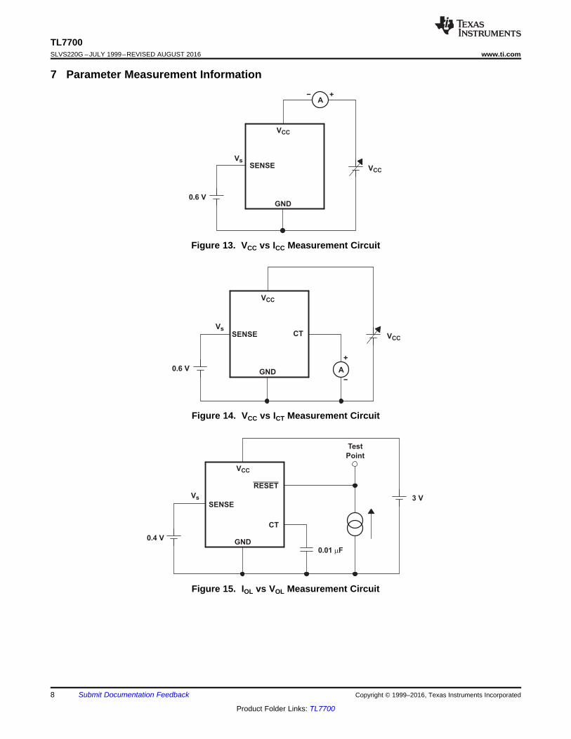
7 Parameter Measurement Information
Figure 13. VCC vs ICC Measurement Circuit
Figure 14. VCC vs ICT Measurement Circuit
Figure 15. IOL vs VOL Measurement Circuit
VCC
Vs
GND
3 V
CT
2.2 kW
100 pF
Test
Point
Ct
RESET
SENSE
Vs
VCC
Vs
GND
VCC
CT
RESET
2.2 kW
0.01 mF
Test
Point
SENSEA+ −
9
TL7700www.ti.com SLVS220G –JULY 1999–REVISED AUGUST 2016
Product Folder Links: TL7700
Submit Documentation FeedbackCopyright © 1999–2016, Texas Instruments Incorporated
Parameter Measurement Information (continued)
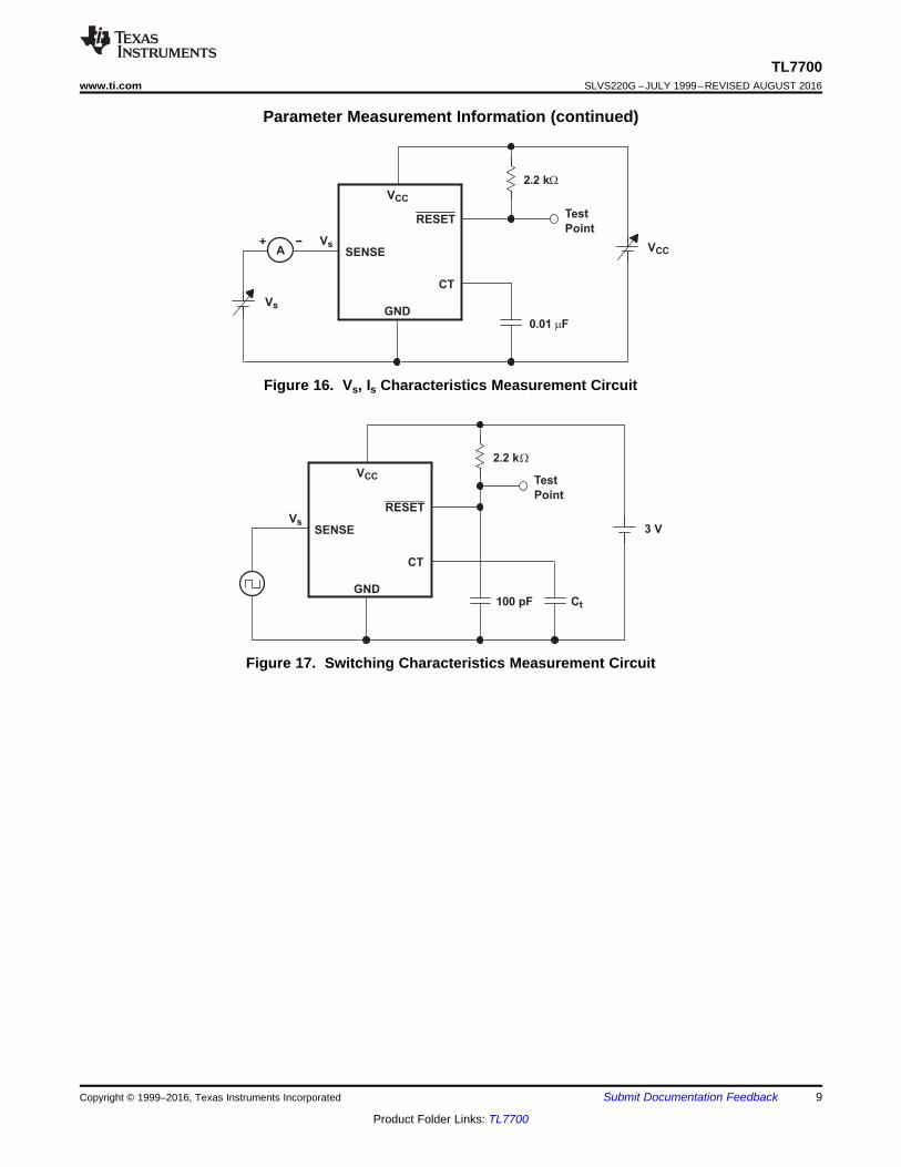
Figure 16. Vs, Is Characteristics Measurement Circuit
Figure 17. Switching Characteristics Measurement Circuit
Reference
Voltage
+
−
+
−
R
S
Q
+
−
Vs = 500 mV TypRESET
GND
CT
SENSE
VCC
ICT(A)
High:
On
IS(A)
Copyright © 2016, Texas Instruments Incorporated
10
TL7700SLVS220G –JULY 1999–REVISED AUGUST 2016 www.ti.com
Product Folder Links: TL7700
Submit Documentation Feedback Copyright © 1999–2016, Texas Instruments Incorporated
8 Detailed Description
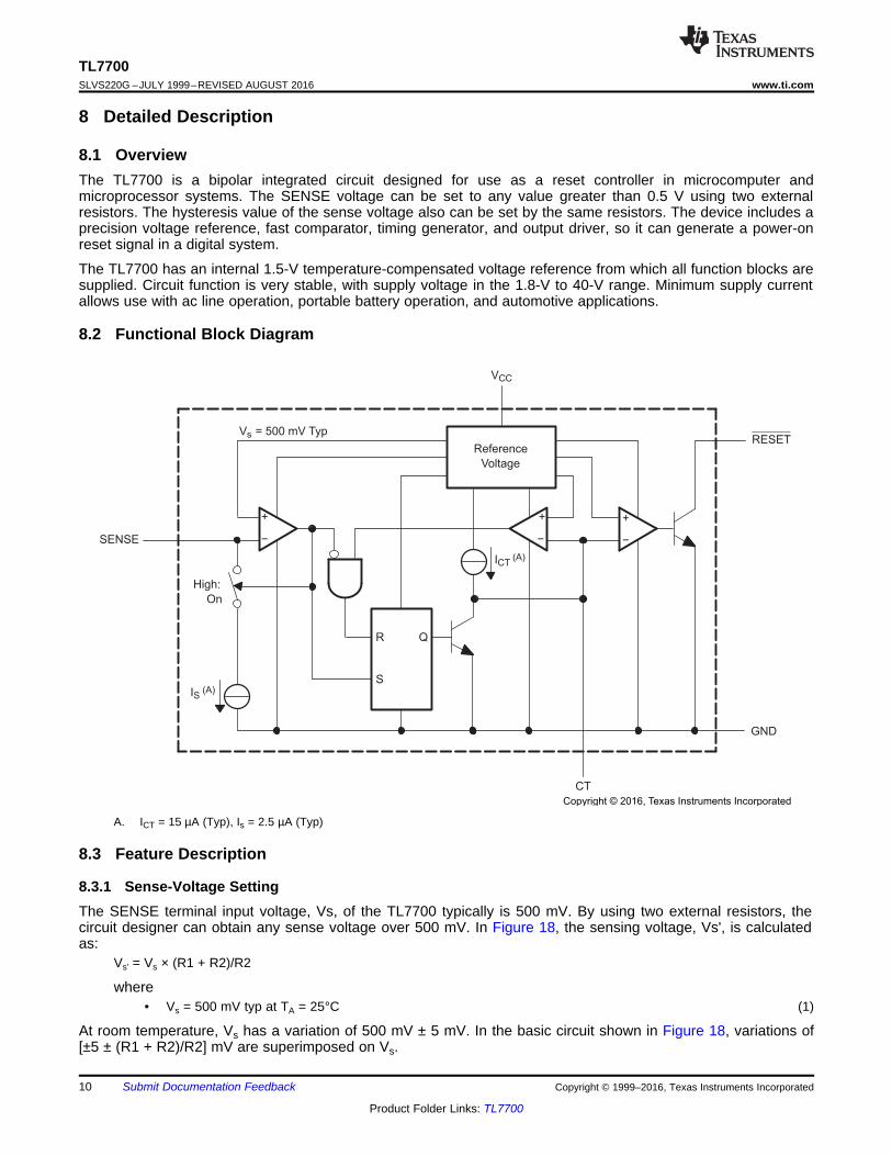
8.1 OverviewThe TL7700 is a bipolar integrated circuit designed for use as a reset controller in microcomputer andmicroprocessor systems. The SENSE voltage can be set to any value greater than 0.5 V using two externalresistors. The hysteresis value of the sense voltage also can be set by the same resistors. The device includes aprecision voltage reference, fast comparator, timing generator, and output driver, so it can generate a power-onreset signal in a digital system.
The TL7700 has an internal 1.5-V temperature-compensated voltage reference from which all function blocks aresupplied. Circuit function is very stable, with supply voltage in the 1.8-V to 40-V range. Minimum supply currentallows use with ac line operation, portable battery operation, and automotive applications.
8.2 Functional Block Diagram
A. ICT = 15 µA (Typ), Is = 2.5 µA (Typ)
8.3 Feature Description
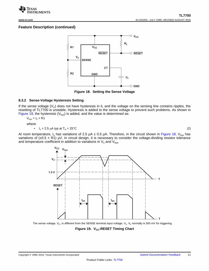
8.3.1 Sense-Voltage SettingThe SENSE terminal input voltage, Vs, of the TL7700 typically is 500 mV. By using two external resistors, thecircuit designer can obtain any sense voltage over 500 mV. In Figure 18, the sensing voltage, Vs', is calculatedas:
Vs' = Vs × (R1 + R2)/R2
where• Vs = 500 mV typ at TA = 25°C (1)
At room temperature, Vs has a variation of 500 mV ± 5 mV. In the basic circuit shown in Figure 18, variations of[±5 ± (R1 + R2)/R2] mV are superimposed on Vs.
tpotpo
RESET
VhysVCC
1.5 V
T
T
Vs’
VCC
Vs
GND
CT
RESET
RL
R1
R2
Ct
VCC
RESET
GND
SENSE
11
TL7700www.ti.com SLVS220G –JULY 1999–REVISED AUGUST 2016
Product Folder Links: TL7700
Submit Documentation FeedbackCopyright © 1999–2016, Texas Instruments Incorporated
Feature Description (continued)
Figure 18. Setting the Sense Voltage
8.3.2 Sense-Voltage Hysteresis SettingIf the sense voltage (Vs') does not have hysteresis in it, and the voltage on the sensing line contains ripples, theresetting of TL7700 is unstable. Hysteresis is added to the sense voltage to prevent such problems. As shown inFigure 19, the hysteresis (Vhys) is added, and the value is determined as:
Vhys = Is × R1
where• Is = 2.5 μA typ at TA = 25°C (2)
At room temperature, Is has variations of 2.5 µA ± 0.5 µA. Therefore, in the circuit shown in Figure 18, Vhys hasvariations of (±0.5 × R1) µV. In circuit design, it is necessary to consider the voltage-dividing resistor toleranceand temperature coefficient in addition to variations in Vs and Vhys.
The sense voltage, Vs', is different from the SENSE terminal input voltage, Vs. Vs normally is 500 mV for triggering.
Figure 19. VCC-RESET Timing Chart
tpotpo
RESET
VhysVCC
1.5 V
T
T
Vs’
12
TL7700SLVS220G –JULY 1999–REVISED AUGUST 2016 www.ti.com
Product Folder Links: TL7700
Submit Documentation Feedback Copyright © 1999–2016, Texas Instruments Incorporated
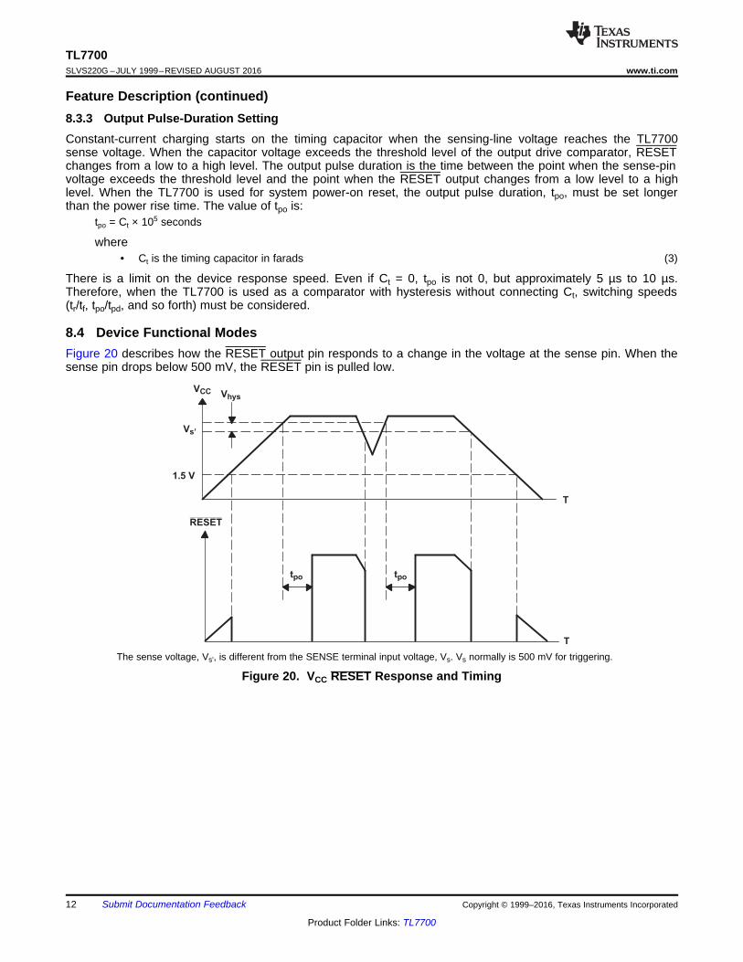
Feature Description (continued)8.3.3 Output Pulse-Duration SettingConstant-current charging starts on the timing capacitor when the sensing-line voltage reaches the TL7700sense voltage. When the capacitor voltage exceeds the threshold level of the output drive comparator, RESETchanges from a low to a high level. The output pulse duration is the time between the point when the sense-pinvoltage exceeds the threshold level and the point when the RESET output changes from a low level to a highlevel. When the TL7700 is used for system power-on reset, the output pulse duration, tpo, must be set longerthan the power rise time. The value of tpo is:
tpo = Ct × 105 seconds
where• Ct is the timing capacitor in farads (3)
There is a limit on the device response speed. Even if Ct = 0, tpo is not 0, but approximately 5 µs to 10 µs.Therefore, when the TL7700 is used as a comparator with hysteresis without connecting Ct, switching speeds(tr/tf, tpo/tpd, and so forth) must be considered.
8.4 Device Functional ModesFigure 20 describes how the RESET output pin responds to a change in the voltage at the sense pin. When thesense pin drops below 500 mV, the RESET pin is pulled low.
The sense voltage, Vs', is different from the SENSE terminal input voltage, Vs. Vs normally is 500 mV for triggering.
Figure 20. VCC RESET Response and Timing
30 k
240 k 2.2 k
TL7700
CT
510 pF
RESET
VCC
SENSE
5V
RESET
VCC
VSS
Microcontroller
GND
Copyright © 2016, Texas Instruments Incorporated
13
TL7700www.ti.com SLVS220G –JULY 1999–REVISED AUGUST 2016
Product Folder Links: TL7700
Submit Documentation FeedbackCopyright © 1999–2016, Texas Instruments Incorporated
9 Application and Implementation
NOTEInformation in the following applications sections is not part of the TI componentspecification, and TI does not warrant its accuracy or completeness. TI’s customers areresponsible for determining suitability of components for their purposes. Customers shouldvalidate and test their design implementation to confirm system functionality.
9.1 Application InformationThe TL7700 supply-voltage supervisor allows for any voltage greater than 500mV to be monitored. This flexibilityallows it to be used in many applications from FPGAs and Microcontrollers to Industrial supply monitoring.
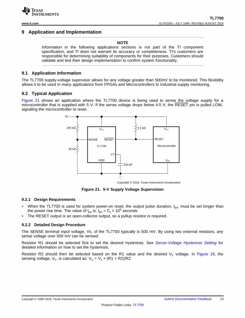
9.2 Typical ApplicationFigure 21 shows an application where the TL7700 device is being used to sense the voltage supply for amicrocontroller that is supplied with 5 V. If the sense voltage drops below 4.5 V, the RESET pin is pulled LOW,signaling the microcontroller to reset.
Figure 21. 5-V Supply Voltage Supervision
9.2.1 Design Requirements• When the TL7700 is used for system power-on reset, the output pulse duration, tpo, must be set longer than
the power rise time. The value of tpo is: tpo = Ct × 105 seconds• The RESET output is an open-collector output, so a pullup resistor is required.
9.2.2 Detailed Design ProcedureThe SENSE terminal input voltage, Vs, of the TL7700 typically is 500 mV. By using two external resistors, anysense voltage over 500 mV can be sensed.
Resistor R1 should be selected first to set the desired hysteresis. See Sense-Voltage Hysteresis Setting fordetailed information on how to set the hysteresis.
Resistor R2 should then be selected based on the R1 value and the desired Vs' voltage. In Figure 18, thesensing voltage, Vs', is calculated as: Vs' = Vs × (R1 + R2)/R2
−75488
490
492
494
496
498
500
502
504
506
−50 −25 0 25 50 75 100 125 150
TA − Free-Air Temperature − °C
TA = 25°C
Vs = 500.8 mV
TA = 25°C
Vs = 498.3 mV
Vs
−S
en
se In
pu
t Vo
ltag
e−
mV
14
TL7700SLVS220G –JULY 1999–REVISED AUGUST 2016 www.ti.com
Product Folder Links: TL7700
Submit Documentation Feedback Copyright © 1999–2016, Texas Instruments Incorporated
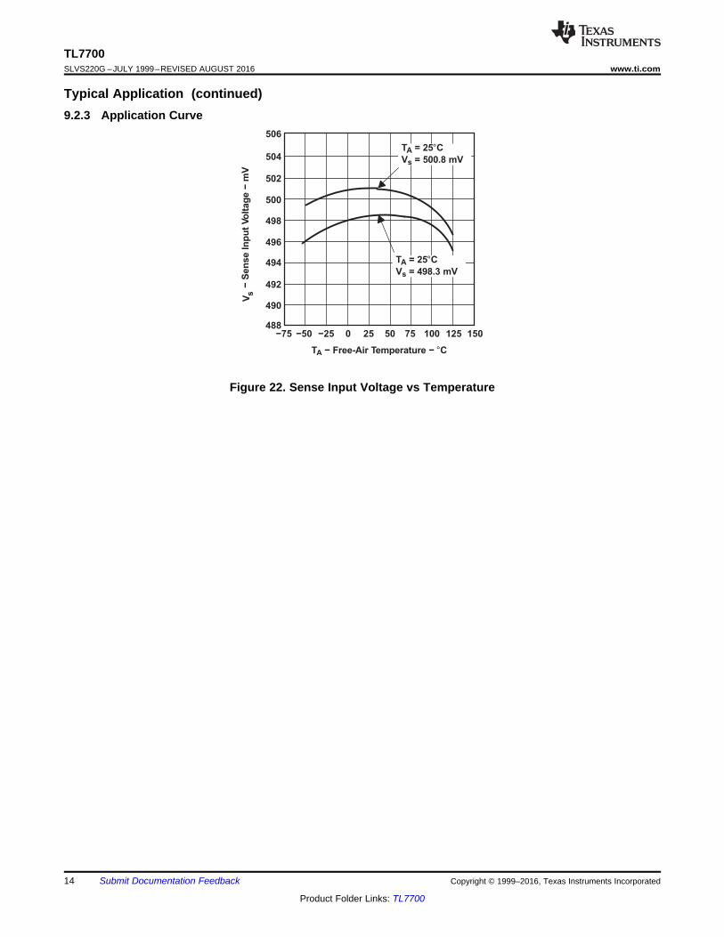
Typical Application (continued)9.2.3 Application Curve
Figure 22. Sense Input Voltage vs Temperature
GND
8
7
6
5
1
2
3
4
5V
NC
CT
GND
VCC
NC
NC
RESET
2.2 k
SENSE
510 pF 30 k
240 k
15
TL7700www.ti.com SLVS220G –JULY 1999–REVISED AUGUST 2016
Product Folder Links: TL7700
Submit Documentation FeedbackCopyright © 1999–2016, Texas Instruments Incorporated
10 Power Supply RecommendationsThe TL7700 device will operate within the supply range specified in Recommended Operating Conditions. Thedevice risks permanent damage over the voltage specified in Absolute Maximum Ratings.
11 Layout
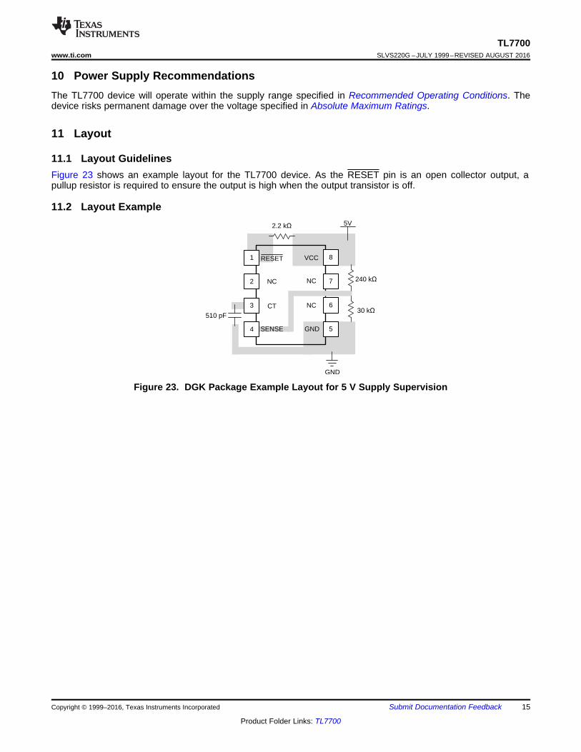
11.1 Layout GuidelinesFigure 23 shows an example layout for the TL7700 device. As the RESET pin is an open collector output, apullup resistor is required to ensure the output is high when the output transistor is off.
11.2 Layout Example
Figure 23. DGK Package Example Layout for 5 V Supply Supervision
16
TL7700SLVS220G –JULY 1999–REVISED AUGUST 2016 www.ti.com
Product Folder Links: TL7700
Submit Documentation Feedback Copyright © 1999–2016, Texas Instruments Incorporated
12 Device and Documentation Support
12.1 Receiving Notification of Documentation UpdatesTo receive notification of documentation updates, navigate to the device product folder on ti.com. In the upperright corner, click on Alert me to register and receive a weekly digest of any product information that haschanged. For change details, review the revision history included in any revised document.
12.2 Community ResourceThe following links connect to TI community resources. Linked contents are provided "AS IS" by the respectivecontributors. They do not constitute TI specifications and do not necessarily reflect TI's views; see TI's Terms ofUse.
TI E2E™ Online Community TI's Engineer-to-Engineer (E2E) Community. Created to foster collaborationamong engineers. At e2e.ti.com, you can ask questions, share knowledge, explore ideas and helpsolve problems with fellow engineers.
Design Support TI's Design Support Quickly find helpful E2E forums along with design support tools andcontact information for technical support.
12.3 TrademarksE2E is a trademark of Texas Instruments.All other trademarks are the property of their respective owners.
12.4 Electrostatic Discharge CautionThis integrated circuit can be damaged by ESD. Texas Instruments recommends that all integrated circuits be handled withappropriate precautions. Failure to observe proper handling and installation procedures can cause damage.
ESD damage can range from subtle performance degradation to complete device failure. Precision integrated circuits may be moresusceptible to damage because very small parametric changes could cause the device not to meet its published specifications.
12.5 GlossarySLYZ022 — TI Glossary.
This glossary lists and explains terms, acronyms, and definitions.
13 Mechanical, Packaging, and Orderable InformationThe following pages include mechanical, packaging, and orderable information. This information is the mostcurrent data available for the designated devices. This data is subject to change without notice and revision ofthis document. For browser-based versions of this data sheet, refer to the left-hand navigation.
PACKAGE OPTION ADDENDUM
www.ti.com 14-Mar-2016
Addendum-Page 1
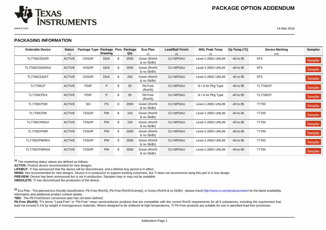
PACKAGING INFORMATION
Orderable Device Status(1)
Package Type PackageDrawing
Pins PackageQty
Eco Plan(2)
Lead/Ball Finish(6)
MSL Peak Temp(3)
Op Temp (°C) Device Marking(4/5)
Samples
TL7700CDGKR ACTIVE VSSOP DGK 8 2500 Green (RoHS& no Sb/Br)
CU NIPDAU Level-1-260C-UNLIM -40 to 85 9TS
TL7700CDGKRG4 ACTIVE VSSOP DGK 8 2500 Green (RoHS& no Sb/Br)
CU NIPDAU Level-1-260C-UNLIM -40 to 85 9TS
TL7700CDGKT ACTIVE VSSOP DGK 8 250 Green (RoHS& no Sb/Br)
CU NIPDAU Level-1-260C-UNLIM -40 to 85 9TS
TL7700CP ACTIVE PDIP P 8 50 Pb-Free(RoHS)
CU NIPDAU N / A for Pkg Type -40 to 85 TL7700CP
TL7700CPE4 ACTIVE PDIP P 8 50 Pb-Free(RoHS)
CU NIPDAU N / A for Pkg Type -40 to 85 TL7700CP
TL7700CPSR ACTIVE SO PS 8 2000 Green (RoHS& no Sb/Br)
CU NIPDAU Level-1-260C-UNLIM -40 to 85 T7700
TL7700CPW ACTIVE TSSOP PW 8 150 Green (RoHS& no Sb/Br)
CU NIPDAU Level-1-260C-UNLIM -40 to 85 T7700
TL7700CPWG4 ACTIVE TSSOP PW 8 150 Green (RoHS& no Sb/Br)
CU NIPDAU Level-1-260C-UNLIM -40 to 85 T7700
TL7700CPWR ACTIVE TSSOP PW 8 2000 Green (RoHS& no Sb/Br)
CU NIPDAU Level-1-260C-UNLIM -40 to 85 T7700
TL7700CPWRE4 ACTIVE TSSOP PW 8 2000 Green (RoHS& no Sb/Br)
CU NIPDAU Level-1-260C-UNLIM -40 to 85 T7700
TL7700CPWRG4 ACTIVE TSSOP PW 8 2000 Green (RoHS& no Sb/Br)
CU NIPDAU Level-1-260C-UNLIM -40 to 85 T7700
(1) The marketing status values are defined as follows:ACTIVE: Product device recommended for new designs.LIFEBUY: TI has announced that the device will be discontinued, and a lifetime-buy period is in effect.NRND: Not recommended for new designs. Device is in production to support existing customers, but TI does not recommend using this part in a new design.PREVIEW: Device has been announced but is not in production. Samples may or may not be available.OBSOLETE: TI has discontinued the production of the device.
(2) Eco Plan - The planned eco-friendly classification: Pb-Free (RoHS), Pb-Free (RoHS Exempt), or Green (RoHS & no Sb/Br) - please check http://www.ti.com/productcontent for the latest availabilityinformation and additional product content details.TBD: The Pb-Free/Green conversion plan has not been defined.Pb-Free (RoHS): TI's terms "Lead-Free" or "Pb-Free" mean semiconductor products that are compatible with the current RoHS requirements for all 6 substances, including the requirement thatlead not exceed 0.1% by weight in homogeneous materials. Where designed to be soldered at high temperatures, TI Pb-Free products are suitable for use in specified lead-free processes.
PACKAGE OPTION ADDENDUM
www.ti.com 14-Mar-2016
Addendum-Page 2
Pb-Free (RoHS Exempt): This component has a RoHS exemption for either 1) lead-based flip-chip solder bumps used between the die and package, or 2) lead-based die adhesive used betweenthe die and leadframe. The component is otherwise considered Pb-Free (RoHS compatible) as defined above.Green (RoHS & no Sb/Br): TI defines "Green" to mean Pb-Free (RoHS compatible), and free of Bromine (Br) and Antimony (Sb) based flame retardants (Br or Sb do not exceed 0.1% by weightin homogeneous material)
(3) MSL, Peak Temp. - The Moisture Sensitivity Level rating according to the JEDEC industry standard classifications, and peak solder temperature.
(4) There may be additional marking, which relates to the logo, the lot trace code information, or the environmental category on the device.
(5) Multiple Device Markings will be inside parentheses. Only one Device Marking contained in parentheses and separated by a "~" will appear on a device. If a line is indented then it is a continuationof the previous line and the two combined represent the entire Device Marking for that device.
(6) Lead/Ball Finish - Orderable Devices may have multiple material finish options. Finish options are separated by a vertical ruled line. Lead/Ball Finish values may wrap to two lines if the finishvalue exceeds the maximum column width.
Important Information and Disclaimer:The information provided on this page represents TI's knowledge and belief as of the date that it is provided. TI bases its knowledge and belief on informationprovided by third parties, and makes no representation or warranty as to the accuracy of such information. Efforts are underway to better integrate information from third parties. TI has taken andcontinues to take reasonable steps to provide representative and accurate information but may not have conducted destructive testing or chemical analysis on incoming materials and chemicals.TI and TI suppliers consider certain information to be proprietary, and thus CAS numbers and other limited information may not be available for release.
In no event shall TI's liability arising out of such information exceed the total purchase price of the TI part(s) at issue in this document sold by TI to Customer on an annual basis.
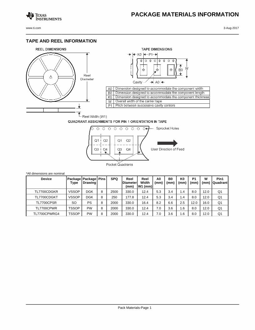
TAPE AND REEL INFORMATION
*All dimensions are nominal
Device PackageType
PackageDrawing
Pins SPQ ReelDiameter
(mm)
ReelWidth
W1 (mm)
A0(mm)
B0(mm)
K0(mm)
P1(mm)
W(mm)
Pin1Quadrant
TL7700CDGKR VSSOP DGK 8 2500 330.0 12.4 5.3 3.4 1.4 8.0 12.0 Q1
TL7700CDGKT VSSOP DGK 8 250 177.8 12.4 5.3 3.4 1.4 8.0 12.0 Q1
TL7700CPSR SO PS 8 2000 330.0 16.4 8.2 6.6 2.5 12.0 16.0 Q1
TL7700CPWR TSSOP PW 8 2000 330.0 12.4 7.0 3.6 1.6 8.0 12.0 Q1
TL7700CPWRG4 TSSOP PW 8 2000 330.0 12.4 7.0 3.6 1.6 8.0 12.0 Q1
PACKAGE MATERIALS INFORMATION
www.ti.com 3-Aug-2017
Pack Materials-Page 1
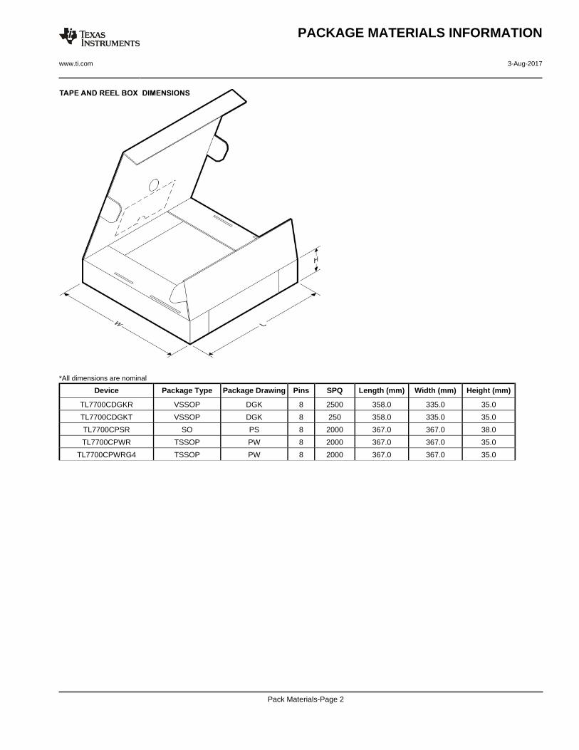
*All dimensions are nominal
Device Package Type Package Drawing Pins SPQ Length (mm) Width (mm) Height (mm)
TL7700CDGKR VSSOP DGK 8 2500 358.0 335.0 35.0
TL7700CDGKT VSSOP DGK 8 250 358.0 335.0 35.0
TL7700CPSR SO PS 8 2000 367.0 367.0 38.0
TL7700CPWR TSSOP PW 8 2000 367.0 367.0 35.0
TL7700CPWRG4 TSSOP PW 8 2000 367.0 367.0 35.0
PACKAGE MATERIALS INFORMATION
www.ti.com 3-Aug-2017
Pack Materials-Page 2
www.ti.com
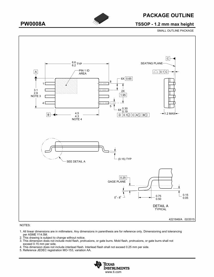
PACKAGE OUTLINE
C
TYP6.66.2
1.2 MAX
6X 0.65
8X 0.300.19
2X1.95
0.150.05
(0.15) TYP
0 - 8
0.25GAGE PLANE
0.750.50
A
NOTE 3
3.12.9
BNOTE 4
4.54.3
4221848/A 02/2015
TSSOP - 1.2 mm max heightPW0008ASMALL OUTLINE PACKAGE
NOTES: 1. All linear dimensions are in millimeters. Any dimensions in parenthesis are for reference only. Dimensioning and tolerancing per ASME Y14.5M. 2. This drawing is subject to change without notice. 3. This dimension does not include mold flash, protrusions, or gate burrs. Mold flash, protrusions, or gate burrs shall not exceed 0.15 mm per side. 4. This dimension does not include interlead flash. Interlead flash shall not exceed 0.25 mm per side.5. Reference JEDEC registration MO-153, variation AA.
18
0.1 C A B
54
PIN 1 IDAREA
SEATING PLANE
0.1 C
SEE DETAIL A
DETAIL ATYPICAL
SCALE 2.800
www.ti.com
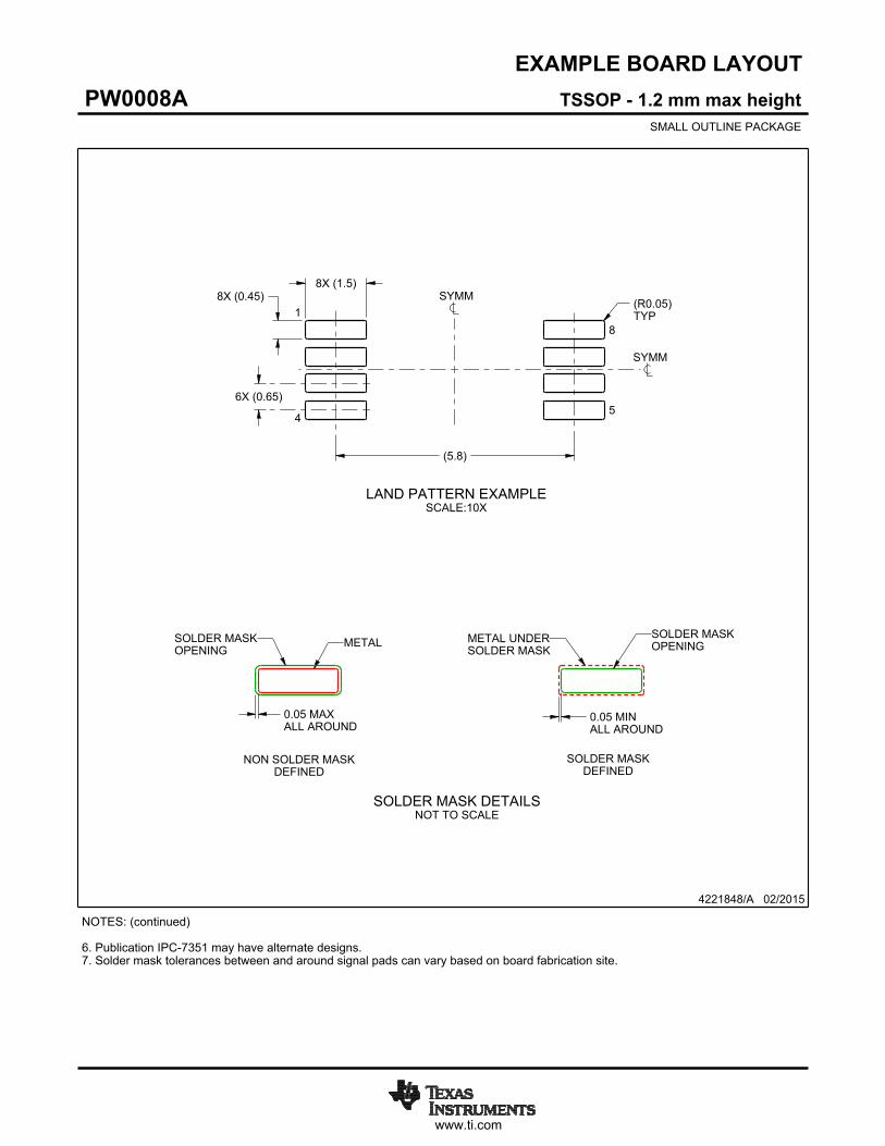
EXAMPLE BOARD LAYOUT
(5.8)
0.05 MAXALL AROUND
0.05 MINALL AROUND
8X (1.5)8X (0.45)
6X (0.65)
(R )TYP
0.05
4221848/A 02/2015
TSSOP - 1.2 mm max heightPW0008ASMALL OUTLINE PACKAGE
SYMM
SYMM
LAND PATTERN EXAMPLESCALE:10X
1
45
8
NOTES: (continued) 6. Publication IPC-7351 may have alternate designs. 7. Solder mask tolerances between and around signal pads can vary based on board fabrication site.
METALSOLDER MASKOPENING
NON SOLDER MASKDEFINED
SOLDER MASK DETAILSNOT TO SCALE
SOLDER MASKOPENING
METAL UNDERSOLDER MASK
SOLDER MASKDEFINED
www.ti.com
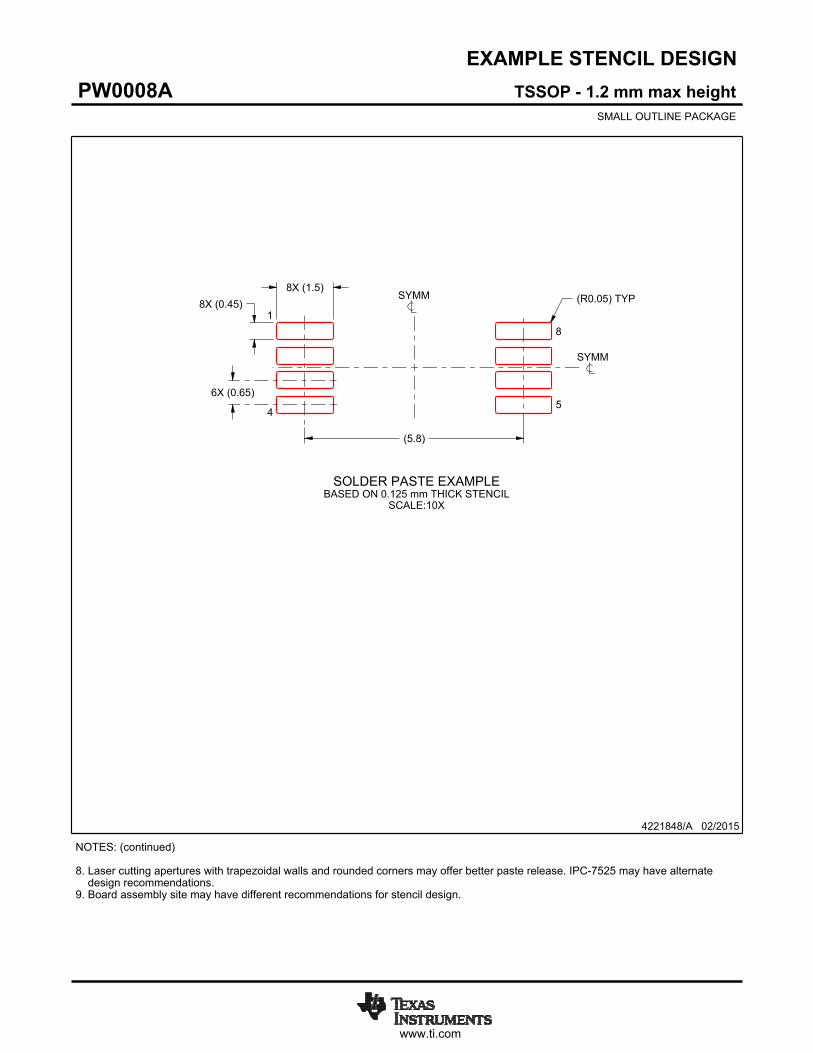
EXAMPLE STENCIL DESIGN
(5.8)
6X (0.65)
8X (0.45)8X (1.5)
(R ) TYP0.05
4221848/A 02/2015
TSSOP - 1.2 mm max heightPW0008ASMALL OUTLINE PACKAGE
NOTES: (continued) 8. Laser cutting apertures with trapezoidal walls and rounded corners may offer better paste release. IPC-7525 may have alternate design recommendations. 9. Board assembly site may have different recommendations for stencil design.
SYMM
SYMM
1
45
8
SOLDER PASTE EXAMPLEBASED ON 0.125 mm THICK STENCIL
SCALE:10X
IMPORTANT NOTICE
Texas Instruments Incorporated (TI) reserves the right to make corrections, enhancements, improvements and other changes to itssemiconductor products and services per JESD46, latest issue, and to discontinue any product or service per JESD48, latest issue. Buyersshould obtain the latest relevant information before placing orders and should verify that such information is current and complete.TI’s published terms of sale for semiconductor products (http://www.ti.com/sc/docs/stdterms.htm) apply to the sale of packaged integratedcircuit products that TI has qualified and released to market. Additional terms may apply to the use or sale of other types of TI products andservices.Reproduction of significant portions of TI information in TI data sheets is permissible only if reproduction is without alteration and isaccompanied by all associated warranties, conditions, limitations, and notices. TI is not responsible or liable for such reproduceddocumentation. Information of third parties may be subject to additional restrictions. Resale of TI products or services with statementsdifferent from or beyond the parameters stated by TI for that product or service voids all express and any implied warranties for theassociated TI product or service and is an unfair and deceptive business practice. TI is not responsible or liable for any such statements.Buyers and others who are developing systems that incorporate TI products (collectively, “Designers”) understand and agree that Designersremain responsible for using their independent analysis, evaluation and judgment in designing their applications and that Designers havefull and exclusive responsibility to assure the safety of Designers' applications and compliance of their applications (and of all TI productsused in or for Designers’ applications) with all applicable regulations, laws and other applicable requirements. Designer represents that, withrespect to their applications, Designer has all the necessary expertise to create and implement safeguards that (1) anticipate dangerousconsequences of failures, (2) monitor failures and their consequences, and (3) lessen the likelihood of failures that might cause harm andtake appropriate actions. Designer agrees that prior to using or distributing any applications that include TI products, Designer willthoroughly test such applications and the functionality of such TI products as used in such applications.TI’s provision of technical, application or other design advice, quality characterization, reliability data or other services or information,including, but not limited to, reference designs and materials relating to evaluation modules, (collectively, “TI Resources”) are intended toassist designers who are developing applications that incorporate TI products; by downloading, accessing or using TI Resources in anyway, Designer (individually or, if Designer is acting on behalf of a company, Designer’s company) agrees to use any particular TI Resourcesolely for this purpose and subject to the terms of this Notice.TI’s provision of TI Resources does not expand or otherwise alter TI’s applicable published warranties or warranty disclaimers for TIproducts, and no additional obligations or liabilities arise from TI providing such TI Resources. TI reserves the right to make corrections,enhancements, improvements and other changes to its TI Resources. TI has not conducted any testing other than that specificallydescribed in the published documentation for a particular TI Resource.Designer is authorized to use, copy and modify any individual TI Resource only in connection with the development of applications thatinclude the TI product(s) identified in such TI Resource. NO OTHER LICENSE, EXPRESS OR IMPLIED, BY ESTOPPEL OR OTHERWISETO ANY OTHER TI INTELLECTUAL PROPERTY RIGHT, AND NO LICENSE TO ANY TECHNOLOGY OR INTELLECTUAL PROPERTYRIGHT OF TI OR ANY THIRD PARTY IS GRANTED HEREIN, including but not limited to any patent right, copyright, mask work right, orother intellectual property right relating to any combination, machine, or process in which TI products or services are used. Informationregarding or referencing third-party products or services does not constitute a license to use such products or services, or a warranty orendorsement thereof. Use of TI Resources may require a license from a third party under the patents or other intellectual property of thethird party, or a license from TI under the patents or other intellectual property of TI.TI RESOURCES ARE PROVIDED “AS IS” AND WITH ALL FAULTS. TI DISCLAIMS ALL OTHER WARRANTIES ORREPRESENTATIONS, EXPRESS OR IMPLIED, REGARDING RESOURCES OR USE THEREOF, INCLUDING BUT NOT LIMITED TOACCURACY OR COMPLETENESS, TITLE, ANY EPIDEMIC FAILURE WARRANTY AND ANY IMPLIED WARRANTIES OFMERCHANTABILITY, FITNESS FOR A PARTICULAR PURPOSE, AND NON-INFRINGEMENT OF ANY THIRD PARTY INTELLECTUALPROPERTY RIGHTS. TI SHALL NOT BE LIABLE FOR AND SHALL NOT DEFEND OR INDEMNIFY DESIGNER AGAINST ANY CLAIM,INCLUDING BUT NOT LIMITED TO ANY INFRINGEMENT CLAIM THAT RELATES TO OR IS BASED ON ANY COMBINATION OFPRODUCTS EVEN IF DESCRIBED IN TI RESOURCES OR OTHERWISE. IN NO EVENT SHALL TI BE LIABLE FOR ANY ACTUAL,DIRECT, SPECIAL, COLLATERAL, INDIRECT, PUNITIVE, INCIDENTAL, CONSEQUENTIAL OR EXEMPLARY DAMAGES INCONNECTION WITH OR ARISING OUT OF TI RESOURCES OR USE THEREOF, AND REGARDLESS OF WHETHER TI HAS BEENADVISED OF THE POSSIBILITY OF SUCH DAMAGES.Unless TI has explicitly designated an individual product as meeting the requirements of a particular industry standard (e.g., ISO/TS 16949and ISO 26262), TI is not responsible for any failure to meet such industry standard requirements.Where TI specifically promotes products as facilitating functional safety or as compliant with industry functional safety standards, suchproducts are intended to help enable customers to design and create their own applications that meet applicable functional safety standardsand requirements. Using products in an application does not by itself establish any safety features in the application. Designers mustensure compliance with safety-related requirements and standards applicable to their applications. Designer may not use any TI products inlife-critical medical equipment unless authorized officers of the parties have executed a special contract specifically governing such use.Life-critical medical equipment is medical equipment where failure of such equipment would cause serious bodily injury or death (e.g., lifesupport, pacemakers, defibrillators, heart pumps, neurostimulators, and implantables). Such equipment includes, without limitation, allmedical devices identified by the U.S. Food and Drug Administration as Class III devices and equivalent classifications outside the U.S.TI may expressly designate certain products as completing a particular qualification (e.g., Q100, Military Grade, or Enhanced Product).Designers agree that it has the necessary expertise to select the product with the appropriate qualification designation for their applicationsand that proper product selection is at Designers’ own risk. Designers are solely responsible for compliance with all legal and regulatoryrequirements in connection with such selection.Designer will fully indemnify TI and its representatives against any damages, costs, losses, and/or liabilities arising out of Designer’s non-compliance with the terms and provisions of this Notice.
Mailing Address: Texas Instruments, Post Office Box 655303, Dallas, Texas 75265Copyright © 2017, Texas Instruments Incorporated