Embed Size (px)
Citation preview
Title Electrochemical Formation of Ca-Si in Molten CaCl2-KCl
Author(s) Sakanaka, Yoshihide; Goto, Takuya; Hachiya, Kan
Citation Journal of The Electrochemical Society (2015), 162(4): D186-D191
Issue Date 2015
URL http://hdl.handle.net/2433/216616
Right
© The Author(s) 2015. Published by ECS. This is an openaccess article distributed under the terms of the CreativeCommons Attribution 4.0 License (CC BY,http://creativecommons.org/licenses/by/4.0/), which permitsunrestricted reuse of the work in any medium, provided theoriginal work is properly cited.
Type Journal Article
Textversion publisher
Kyoto University

D186 Journal of The Electrochemical Society, 162 (4) D186-D191 (2015)
Electrochemical Formation of Ca-Si in Molten CaCl2-KClY. Sakanaka,a,z T. Goto,a and Kan Hachiyab
aDepartment of Science of Environment and Mathematical Modeling, Graduate School of Science and Engineering,Doshisha University, Kyoto, JapanbGraduate School of Energy Science, Kyoto University, Kyoto, Japan
Electrochemical formation of a Ca-Si film in a molten CaCl2-KCl at 923 K was investigated. Potentiostatic electrolysis of a Sielectrode at −0.10 V for 1 h resulted in the formation of a multiphase Ca-Si film having a thickness of about 30 μm. The Ca-Sifilm was converted into other alloy phases by anodic potentiostatic electrolysis after the cathodic electrodeposition of Ca metal at−0.10 V. The various transformation reactions and the corresponding equilibrium potentials were clarified. At 923 K, the equilibriumpotential was found to be 0.18 V (CaSi2). Reflectance measurements in the ultraviolet, visible, and near-infrared region clarified thatthe CaSi2 film has a direct bandgap of 3.1 eV.© The Author(s) 2015. Published by ECS. This is an open access article distributed under the terms of the Creative CommonsAttribution 4.0 License (CC BY, http://creativecommons.org/licenses/by/4.0/), which permits unrestricted reuse of the work in anymedium, provided the original work is properly cited. [DOI: 10.1149/2.1021504jes] All rights reserved.
Manuscript submitted December 11, 2014; revised manuscript received January 26, 2015. Published February 14, 2015.
Compound semiconductors are among the most promising materi-als for use in high-power electronic and photoelectric conversion de-vices because of their advantages.1 However, conventional processesfor preparing semiconductors involve high energy consumption andthe use of hazardous starting materials, and are hence unsuitable formass production. Therefore, a new semiconductor preparation pro-cess that does not require harmful starting materials or high energyhas been proposed.
Recently, metal silicides, which are abundant, non-toxic mate-rials, have attracted much interest for use as environment-friendlysemiconductors, because they are expected to show excellent opticalproperties. In addition, the bandgap energy of metal silicides can beextended from the infrared to the visible region by appropriate choiceof metal elements and phases of the compounds.2–5
Among the numerous metal silicides reported, Ca-Si metal sili-cides are well known semiconductor materials that exhibit supercon-ductive properties. For example, Ca2Si is a semiconductor with anenergy gap of 1.9 eV,6 while CaSi is expected to show high hydro-gen storage capacity.7 In addition, superconductivity has been dis-covered at 14 K under pressure in a new polymorph of the CaSi2
stoichiometry.8,9 Recently, there has been increased interest in the useof intermetallic silicides to replace the conventional graphite anodesin Li-ion batteries.10,11 Films fabricated from these alloys, with arbi-trary shapes and sizes, may be used in various applications such asenergy conversion devices.
Nevertheless, the high vapor pressure of Ca makes the growth of acontinuous film layer by deposition from the gas phase12–17 difficult.Ca atoms are easily evaporated from the Si substrate, which preventsthe formation of Ca-silicide by interdiffusion with the Si substrate.
With this background, we proposed a novel electrochemical pro-cess for the formation of silicide films. This process is advantageousbecause (1) the phases of the alloy films can be controlled by adjust-ing the electrochemical parameters and (2) the films can be grown onsubstrates of various shapes. We chose a calcium silicide as a model toconfirm the feasibility of this process for producing silicide films, andinvestigated the electrodeposition of Ca and Si to form Ca-Si alloysin a molten CaCl2-KCl system at 923 K.
Experimental
CaCl2 (95.0%, Wako Pure Chemical Co. Ltd.) and KCl (99.5%,Wako Pure Chemical Co. Ltd.) were mixed in eutectic composition(CaCl2:KCl = 38.4:61.6 mol%), and introduced in a high-purity alu-mina crucible (99.5 wt% Al2O3, SSA-S grade, NIKKATO Co. Ltd.),which was then kept under vacuum for more than 24 h at 473 K toensure complete removal of water. All experiments were performed in
zE-mail: [email protected]
the CaCl2-KCl eutectic melt in a dry argon atmosphere. Temperaturemeasurements were performed using a Chromel-Alumel thermocou-ple, with an accuracy of ±1 K. To investigate the electrochemicalbehavior, n-type Si plates (5 mm × 20 mm × 0.5 mm; 99.5%, NilacoCo. Ltd.) were used as the working electrodes. The reference elec-trode was a silver wire immersed in CaCl2-KCl containing 1 mol% ofAgCl, placed in an alumina tube with a thin bottom to maintain elec-trical contact with the melt. The potential of the reference electrodewas calibrated with reference to that of a Mn+/M electrode, whichwas prepared by electrodepositing an alkali metal on Mo wire. Allpotentials referred to in this paper are expressed with reference tothe Mn+/M potential. The counter electrode was a glassy carbon rod(3 mm diameter; Tokai Carbon Co. Ltd.). A potentiostat/galvanostat(Hokuto Denko Co. Ltd. HZ-3000) was used for cyclic voltammetryand chronopotentiometry measurements. The samples were preparedby potentiostatic electrolysis and rinsed with ethylene glycol. The ob-tained samples were analyzed by X-ray diffractometry (XRD) witha Cu Kα line. The surface and cross-section of the samples wereobserved by scanning electron microscopy (SEM; JSM-7001, JEOL).For evaluation of the optical properties of the films, ultraviolet-visible-near infrared (UV-VIS-NIR) reflectance spectra were measured usinga JASCO V-670 spectrophotometer.
Results and Discussion
Electrochemical window of CaCl2-KCl.— Figure 1 shows thecyclic voltammograms obtained in CaCl2-KCl at 923 K. A molybde-num wire and a glassy carbon rod were used as the working electrodesin the negative and positive potential regions, respectively. In the neg-ative potential region, a sharp cathodic current and the correspondinganodic current were observed at about 0.10 V, which were attributableto the deposition of Ca or K metal and dissolution of the deposits,respectively. The current observed at a potential more negative than0.4 V is due to the formation of Ca metal (activity smaller than 1) andits dissolution in CaCl2. The potential at the cathodic limit was de-fined as the potential of the Mn+/M electrode prepared by the followingprocedure. Galvanostatic electrolysis was conducted at –50 mA cm−2
using a molybdenum electrode for 20 s, and then, the open-circuit po-tential was measured, as shown in Figure 2. The potential measuredimmediately after the electrolysis was the Mn+/M potential.
In the positive potential region of the cyclic voltammogram, theanodic current increased from about 3.40 V, as shown in Figure 3.Because chloride ions were the only anions in this melt, the anodiccurrents were considered to be due to the oxidation of chloride ionsto chlorine gas.
2Cl− → Cl2 + 2e− [1]
After the potential sweep direction was reversed (to negative),the current constantly decreased, eventually falling to zero at 3.46 V.
) unless CC License in place (see abstract). ecsdl.org/site/terms_use address. Redistribution subject to ECS terms of use (see 130.54.110.32Downloaded on 2016-09-19 to IP

Journal of The Electrochemical Society, 162 (4) D186-D191 (2015) D187
Figure 1. Cyclic voltammograms for a Mo electrode in CaCl2-KCl at 923 K.Scanning rate: 0.1 Vs−1.
This potential was defined as the potential of the anodic limit, since itis regarded as the Cl2/Cl− potential. From the CV results, the electro-chemical window was determined to be 3.46 V.
Cyclic voltammetry.— In order to investigate the electrochemicalbehavior of the calcium ions, cyclic voltammetry was conducted inmolten CaCl2-KCl at 923 K. Figure 4 shows the cyclic voltammo-grams for a Si electrode at a scanning rate of 0.1 V s−1 at 923 K.
The electrochemical behavior of a Mo electrode was also investi-gated for comparison, because Mo does not form an alloy with Ca.18
Figure 4 shows the typical cyclic voltammograms for Mo and Si elec-trodes at a scanning rate of 0.1 V s−1. For the Mo electrode, a sharpincrease in the cathodic current was observed at 0.2 V. Since Mo doesnot form alloys with Ca and K, the cathodic current was consideredto be due to Ca or K metal deposition. After reversing the scanningdirection at 0.10 V, a large anodic current peak was observed, becauseof the anodic dissolution of Ca or K metal.
Figure 2. Open-circuit potential transient curve for the Mo electrode in theCaCl2-KCl system at 923 K. Before the measurement, Ca metal was elec-trodeposited at the electrode by galvanostatic electrolysis at −50 mA cm−2
for 20 s.
Figure 3. Cyclic voltammogram for a glassy carbon electrode in CaCl2-KClat 923 K. Scanning rate: 0.1 Vs−1.
For the Si electrode, cathodic currents were observed from1.20 V. Since this potential was more positive than the potential for Cametal deposition, the cathodic currents were attributed to the forma-tion of Ca-Si alloys. The standard formal potentials of Ca2Si, CaSi,and CaSi2 were 0.35, 0.46, and 0.49 V, respectively, as calculated fromthe corresponding standard Gibbs energies of formation.19 These re-sults agreed with those deduced from the cyclic voltammogram inFigure 4.
When the potential scan direction was reversed at −0.10 V, severalanodic peaks were observed at 0.35, 0.65, and 1.00 V, respectively,indicating Ca dissolution from the different Ca-Si alloy phases.
Formation of Ca-Si alloy.— Based on the results of cyclic voltam-metry, an alloy sample was prepared by potentiostatic electrolysis ona Si electrode at −0.10 V for 1 h. Figure 5 shows the XRD pattern ofthe sample. The spectrum showed peaks assignable to CaSi, CaSi2,and the Si substrate, along with several unknown peaks.
Figure 4. Cyclic voltammograms for Mo and Si electrode in CaCl2-KCl at923 K. Scanning rate: 0.1 V s−1.
) unless CC License in place (see abstract). ecsdl.org/site/terms_use address. Redistribution subject to ECS terms of use (see 130.54.110.32Downloaded on 2016-09-19 to IP

D188 Journal of The Electrochemical Society, 162 (4) D186-D191 (2015)
Figure 5. XRD pattern of the sample obtained by potentiostatic electrolysiswith a Si electrode at −0.10 V for 1 h in CaCl2-KCl eutectic at 923 K.
Figure 6 shows a cross-sectional SEM image of the sample and theconcentration profiles of Ca and Si obtained by EDS line analysis. Theobserved alloy layer with a thickness of approximately 30 μm wasconsidered to comprise CaSi and CaSi2 layers, in accordance with theXRD result.
Phase control of Ca-Si.— The phase diagram of the Ca-Si systemis shown in Figure 7.18 According to this diagram, three Ca-Si in-termetallic compounds having Ca concentrations lower than those ofCaSi2, CaSi, and Ca2Si should exist at 923 K.
Figure 6. Cross-sectional SEM image and concentration profiles of Ca andSi for the sample at −0.10 V for 1 h.
Chronopotentiometry measurements were conducted to confirmthe possibility of formation of Ca-Si alloy phases.
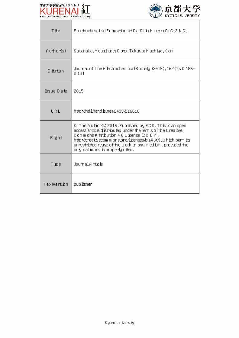
Open-circuit potentiometry was carried out to further investigatethe formation of Ca-Si alloys. Figure 8 shows the open circuit potentialtransient curve for a Si electrode after the deposition of Ca metal bygalvanostatic electrolysis at −50 mA cm−2 for 60 s, in molten CaCl2-KCl at 923 K.
As can be seen in the chronopotentiogram, the potential remainedat 0 V for the initial 10 s, probably because of the presence of thedeposited Ca metal on the electrode. Subsequently, plateaus wereobserved at 0.18, 0.47, and 0.57 V, which were possibly due to differentcoexisting Ca-Si phases. Based on this result, samples were preparedby potentiostatic electrolysis.
First, potentiostatic electrolysis was conducted at −0.10 V for30 min. Then, anodic dissolutions of Ca were conducted for 30 min
Figure 7. Phase diagram of the Ca-Si system.18
) unless CC License in place (see abstract). ecsdl.org/site/terms_use address. Redistribution subject to ECS terms of use (see 130.54.110.32Downloaded on 2016-09-19 to IP
Journal of The Electrochemical Society, 162 (4) D186-D191 (2015) D189
Figure 8. Open-circuit potential transient curve for the Si electrode in CaCl2-KCl system at 923 K. Before the measurement, Ca metal was electrodepositedat the electrode by galvanostatic electrolysis at −50 mA cm−2 for 30 s.
by potentiostatic electrolysis at 0.10 (sample 1), 0.37 (sample 2),0.50 (sample 3), and 0.78 V (sample 4). These potential values weredetermined by taking into account the potential plateaus before andafter the potential jump indicating complete phase change.
The phases of the samples were analyzed by XRD, and the crosssections of the samples were observed by SEM.
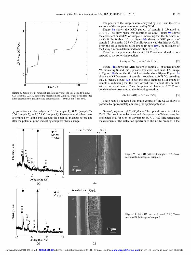
Figure 9a shows the XRD pattern of sample 1 (obtained at0.10 V). The alloy phase was identified as CaSi. Figure 9b showsthe cross-sectional SEM of sample 1, indicating that the thickness ofthe CaSi film is about 10 μm. Figure 10a shows the XRD patterns ofsample 2 (obtained at 0.37 V). The alloy phase was identified as CaSi2.From the cross-sectional SEM image (Figure 10b), the thickness ofthe CaSi2 film was determined to be about 20 μm.
Therefore, the potential plateau at 0.18 V was considered to cor-respond to the following reaction:
CaSi2 + Ca (II) + 2e− ⇔ 2CaSi [2]
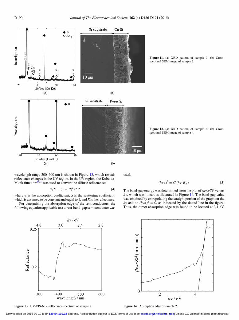
Figure 11a shows the XRD pattern of sample 3 (obtained at 0.50V), indicating Si and CaSi2 phases. The cross-sectional SEM imagein Figure 11b shows the film thickness to be about 20 μm. Figure 12ashows the XRD patterns of sample 4 (obtained at 0.78 V), revealingonly Si peaks. Figure 12b shows the cross-sectional SEM image ofsample 4, indicating that the transformed film is about 20 μm thickwith a porous structure. Thus, the potential plateau at 0.57 V wasconsidered to correspond to the following reaction:
2Si + Ca (II) + 2e− ⇔ CaSi2 [3]
These results suggested that phase control of the Ca-Si alloys ispossible by appropriately adjusting the applied potential.
Optical properties of Ca-Si film.— The optical properties of theCa-Si film, such as reflectance and absorption coefficient, were in-vestigated as a function of wavelength by UV-VIS-NIR reflectancemeasurements. The reflection spectrum of the Ca-Si product in the
Figure 9. (a) XRD pattern of sample 1. (b) Cross-sectional SEM image of sample 1.
Figure 10. (a) XRD pattern of sample 2. (b) Cross-sectional SEM image of sample 2.
) unless CC License in place (see abstract). ecsdl.org/site/terms_use address. Redistribution subject to ECS terms of use (see 130.54.110.32Downloaded on 2016-09-19 to IP
D190 Journal of The Electrochemical Society, 162 (4) D186-D191 (2015)
Figure 11. (a) XRD pattern of sample 3. (b) Cross-sectional SEM image of sample 3.
Figure 12. (a) XRD pattern of sample 4. (b) Cross-sectional SEM image of sample 4.
wavelength range 300–600 nm is shown in Figure 13, which revealsreflectance changes in the UV region. In the UV region, the Kubelka-Munk function20,21 was used to convert the diffuse reflectance:
α/S = (1 − R)2/2R [4]
where α is the absorption coefficient, S is the scattering coefficient,which is assumed to be constant and equal to 1, and R is the reflectance.
For determining the absorption edge of the semiconductors, thefollowing equation applicable to a direct-band-gap semiconductor was
Figure 13. UV-VIS-NIR reflectance spectrum of sample 2.
used.
(hνα)2 = C (hν-Eg) [5]
The band-gap energy was determined from the plot of (hνα/S)2 versushν, which was linear, as illustrated in Figure 14. The band-gap valuewas obtained by extrapolating the straight portion of the graph on thehν axis to (hνα)2 = 0, as indicated by the dotted line in the figure.Thus, the direct absorption edge was found to be located at 3.1 eV.
Figure 14. Absorption edge of sample 2.
) unless CC License in place (see abstract). ecsdl.org/site/terms_use address. Redistribution subject to ECS terms of use (see 130.54.110.32Downloaded on 2016-09-19 to IP

Journal of The Electrochemical Society, 162 (4) D186-D191 (2015) D191
From the present measurements, the bandgap of CaSi2 was confirmedto be in the ultraviolet region.
Conclusions
The electrochemical formation of a Ca-Si alloy was investigatedin CaCl2-KCl at 923 K. The electrochemical window of CaCl2-KClwas found to be 3.46 V at 923 K. Potentiostatic electrolysis of a Sielectrode at −0.10 V resulted in the formation of a multiphase Ca-Sifilm having a thickness of about 30 μm. The multiphase Ca-Si filmwas converted into a CaSi, CaSi2, or Si phase by anodic potentiostaticelectrolysis depending on the potential. The various transformationreactions and the corresponding equilibrium potentials were clarified.UV-VIS-NIR reflectance measurements confirmed that the bandgapof CaSi2 is 3.1 eV with a direct absorption edge.
References
1. H. Lange, Phys. Stat. Sol. B, 201, 3 (1997).2. M. Eizenberg and K. N. Tu, J. Appl. Phys., 53, 6885 (1982).
3. K. Lefki, P. Muret, N. Cherief, and C. Cinti, J. Appl. Phys., 69, 352 (1991).4. J. F. Morar and M. Wittmer, Phys. Rev., B 37, 2618 (1998).5. Y. Imai, A. Watanabe, and M. Mukaida, J. Alloy Comp., 358, 257 (2003).6. O. Madelung, Semiconductors basic data, 2nd ed., Springer, Berlin (1996).7. M. Aoki, N. Ohba, T. Noritake, and S. Towata, Appl. Phys. Lett., 85, 387 (2004).8. S. Sanfilippo, H. Elsinger, M. Nunez-Reguerio, and O. Laborde, Phys. Rev., B 61,
R3800 (2000).9. G. Satta, G. Profeta, F. Bernadini, A. Continenza, and S. Massidda, Phys. Rev. B, 64,
104507 (2001).10. A. Netz, R. A. Huggins, and W. Weppner, J. Power Sources., 119, 95 (2003).11. J Wolfenstine, J. Power Sources., 124, 241 (2003).12. H. N. Acharya, S. K. Dutta, and H. D. Banerjee, Sol. Ene. Mat., 3, 441 (1980).13. T. Koga, A. Bright, T. Suzuki, K. Shimada, H Tatsuoka, and H. Kuwabara, Thin Sol.
Films., 369, 248 (2000).14. M. Sugiyama and Y. Maeda, Thin Sol. Films., 381, 225 (2001).15. T. Nakamura, T. Suematsu, K. Takakura, F. Hasegawa, A. Wakahara, and M. Imai,
Appl. Phys. Lett., 81, 1032 (2002).16. T. Hosono, Y. Matsuzawa, M. Kuramoto, Y. Momose, H. Tatsuoka, and H. Kuwabara,
Solid State Phenom., 93, 447 (2003).17. Iu. Kogut and M. C. Record, Intermetallics., 32, 184 (2013).18. T. B. Massalski, Binary Alloy Phase Diagrams, Vol. 2, Editor, ASM International,
p. 953 (1990).19. F∗A∗C∗T, http://www.crct.polymtl.ca/reacweb.htm.20. P. Kubelka and F. Munk, Z. Tech. Phys., 12, 593 (1931).21. P. Kubelka, J. Opt. Soc. Am., 38, 448 (1948).
) unless CC License in place (see abstract). ecsdl.org/site/terms_use address. Redistribution subject to ECS terms of use (see 130.54.110.32Downloaded on 2016-09-19 to IP