Embed Size (px)
Citation preview
BASIC ELECTRICAL ENGINEERING LAB. MANUAL
Page | 1
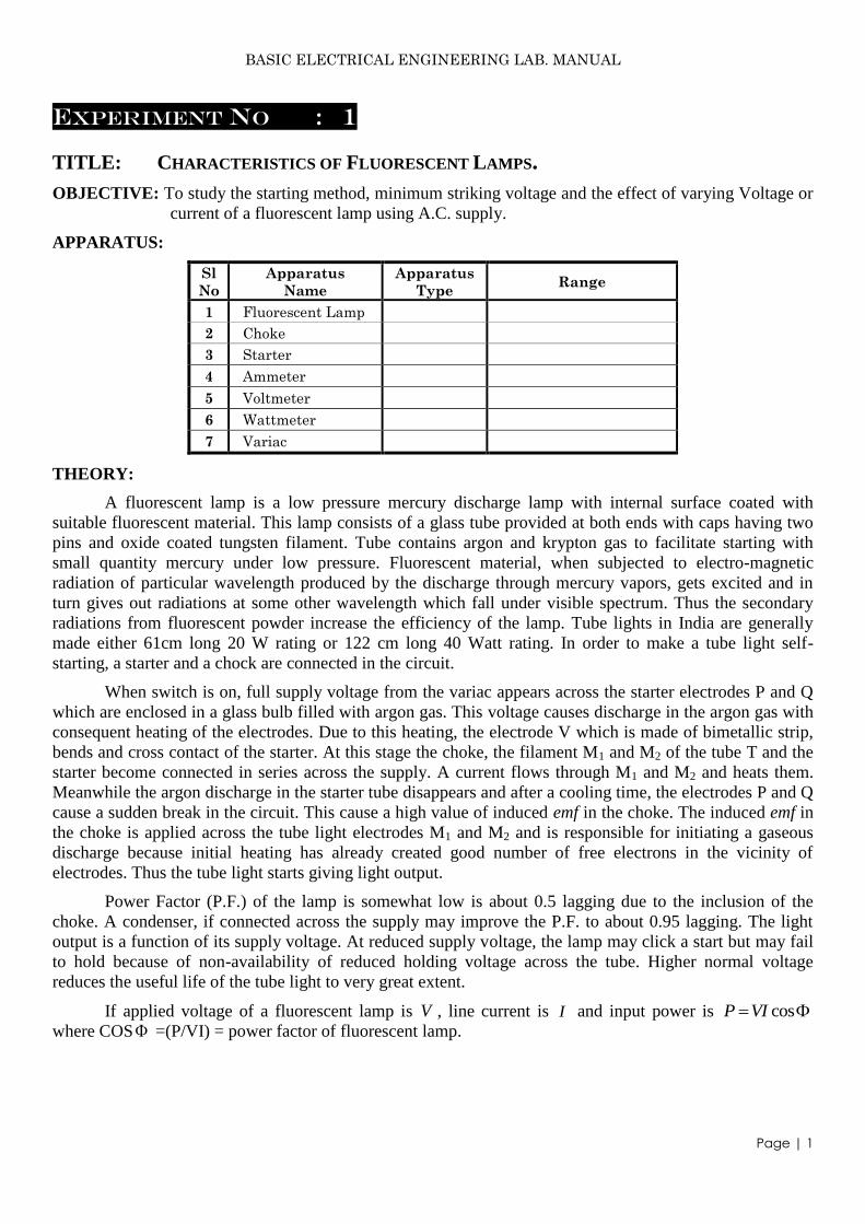
EXPERIMENT NO : 1
TITLE: CHARACTERISTICS OF FLUORESCENT LAMPS.
OBJECTIVE: To study the starting method, minimum striking voltage and the effect of varying Voltage or
current of a fluorescent lamp using A.C. supply.
APPARATUS:
Sl
No
Apparatus
Name
Apparatus
Type Range
1 Fluorescent Lamp
2 Choke
3 Starter
4 Ammeter
5 Voltmeter
6 Wattmeter
7 Variac
THEORY:
A fluorescent lamp is a low pressure mercury discharge lamp with internal surface coated with
suitable fluorescent material. This lamp consists of a glass tube provided at both ends with caps having two
pins and oxide coated tungsten filament. Tube contains argon and krypton gas to facilitate starting with
small quantity mercury under low pressure. Fluorescent material, when subjected to electro-magnetic
radiation of particular wavelength produced by the discharge through mercury vapors, gets excited and in
turn gives out radiations at some other wavelength which fall under visible spectrum. Thus the secondary
radiations from fluorescent powder increase the efficiency of the lamp. Tube lights in India are generally
made either 61cm long 20 W rating or 122 cm long 40 Watt rating. In order to make a tube light self-
starting, a starter and a chock are connected in the circuit.
When switch is on, full supply voltage from the variac appears across the starter electrodes P and Q
which are enclosed in a glass bulb filled with argon gas. This voltage causes discharge in the argon gas with
consequent heating of the electrodes. Due to this heating, the electrode V which is made of bimetallic strip,
bends and cross contact of the starter. At this stage the choke, the filament M1 and M2 of the tube T and the
starter become connected in series across the supply. A current flows through M1 and M2 and heats them.
Meanwhile the argon discharge in the starter tube disappears and after a cooling time, the electrodes P and Q
cause a sudden break in the circuit. This cause a high value of induced emf in the choke. The induced emf in
the choke is applied across the tube light electrodes M1 and M2 and is responsible for initiating a gaseous
discharge because initial heating has already created good number of free electrons in the vicinity of
electrodes. Thus the tube light starts giving light output.
Power Factor (P.F.) of the lamp is somewhat low is about 0.5 lagging due to the inclusion of the
choke. A condenser, if connected across the supply may improve the P.F. to about 0.95 lagging. The light
output is a function of its supply voltage. At reduced supply voltage, the lamp may click a start but may fail
to hold because of non-availability of reduced holding voltage across the tube. Higher normal voltage
reduces the useful life of the tube light to very great extent.
If applied voltage of a fluorescent lamp is V , line current is I and input power is cosP VI where COS =(P/VI) = power factor of fluorescent lamp.
BASIC ELECTRICAL ENGINEERING LAB. MANUAL
Page | 2
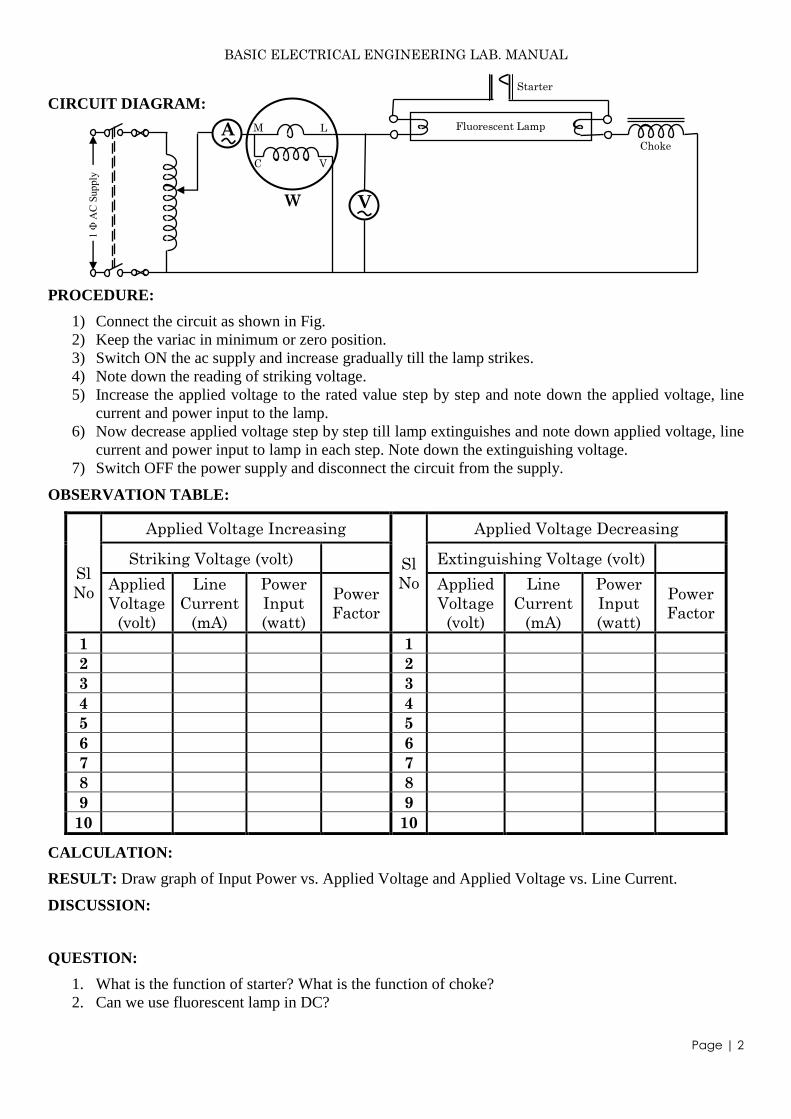
CIRCUIT DIAGRAM:
PROCEDURE:
1) Connect the circuit as shown in Fig.
2) Keep the variac in minimum or zero position.
3) Switch ON the ac supply and increase gradually till the lamp strikes.
4) Note down the reading of striking voltage.
5) Increase the applied voltage to the rated value step by step and note down the applied voltage, line
current and power input to the lamp.
6) Now decrease applied voltage step by step till lamp extinguishes and note down applied voltage, line
current and power input to lamp in each step. Note down the extinguishing voltage.
7) Switch OFF the power supply and disconnect the circuit from the supply.
OBSERVATION TABLE:
Sl
No
Applied Voltage Increasing
Sl
No
Applied Voltage Decreasing
Striking Voltage (volt) Extinguishing Voltage (volt)
Applied
Voltage
(volt)
Line
Current
(mA)
Power
Input
(watt)
Power
Factor
Applied
Voltage
(volt)
Line
Current
(mA)
Power
Input
(watt)
Power
Factor
1 1
2 2
3 3
4 4
5 5
6 6
7 7
8 8
9 9
10 10
CALCULATION:
RESULT: Draw graph of Input Power vs. Applied Voltage and Applied Voltage vs. Line Current.
DISCUSSION:
QUESTION:
1. What is the function of starter? What is the function of choke?
2. Can we use fluorescent lamp in DC?
M L
C V
W
1 Φ
AC
Sup
ply
A
V
Starter
Choke
Fluorescent Lamp
BASIC ELECTRICAL ENGINEERING LAB. MANUAL
Page | 3
EXPERIMENT NO : 2
TILLE: CHARACTERISTICS OF TUNGSTEN FILAMENT LAMPS
OBJECTIVE : To study and draw the following characteristics of Tungsten Filament Lamp
I. Voltage vs. Current
II. Resistance vs. Voltage
III. Voltage vs. Power
APPARATUS:
Sl
No
Apparatus
Name
Apparatus
Type Range
1 Tungsten Lamp
2 Ammeter
3 Voltmeter
4 Wattmeter
5 Variac
THEORY:
There are two types of lamps which are in common use, one is filament lamp and the other is
gaseous discharge lamp. The filament lamps are incandescent lamps, e.g. carbon, tungsten etc. The filament
of these lamps, when heated due to electric current, emits radiations in visible spectrum. The filament of
incandescent lamp is mostly made of tungsten wire whose melting point is 34000C. At normal working
voltage, the filament material gets heated to a very high temperature and emits white light. The filament is
made in the form of a coiled-coil to contain a longer length of the filament in a shorter space and is enclosed
in an evacuated glass bulb to minimize oxidation of filament material at such a high operating temperature.
Usually the lamps above 15w or 25w are filled with an inert gas, e.g. argon or nitrogen, to enable the
filament to operate at higher temperatures and achieve higher lumens/watt efficiency (in the range of 12-
13watt).
The resistance of filament changes considerably when switched on. The initial resistance of the
filament in cold condition can be measured by multi-meter or by ammeter-voltmeter method. The filament
resistance at normal operating temperature is difficult to measure directly and is therefore, calculated by
using the following relation:
R = W/I2
Ω
Where, R = Resistance in ohm when normal voltage is applied across the lamp
I = Current taken by the lamp in ampere.
W= Power to the lamp in Watt
Basic reason of getting all these conductors heated is their resistance. Resistance is the physical
property of a substance by virtue of which it opposes the flow of current through it. Conductors offer lower
resistance than insulators.
Experiments have shown that the resistivity is affected by the conductor’s temperature. The
resistivity and, hence, the resistance of most of the conducting materials increases with increase in
temperature. The resistance changes with temperature according to the relation:
0 01TR R T T
Where TR and
0R are the value of resistances of the conductor at T and 0T respectively and α is a
constant called temperature coefficient of resistance. 0T is often taken to be either room temperature or 0° C.
BASIC ELECTRICAL ENGINEERING LAB. MANUAL
Page | 4
The value of is very small for pure metal, so their resistance increase with increasing temperature. The
temperature co-efficient of Tungsten Filament and Carbon Filament lamp are 0.0045 and – 0.0005
respectively.
CIRCUIT DIAGRAM:
PROCEDURE:
1) Connect the circuit diagram as shown in Fig.
2) Keep the variac in minimum or zero position.
3) Switch ON the power supply and increase the applied voltage gradually in step by step.
4) Note down the applied voltage, load current and input power for every step.
5) Switch OFF power supply and disconnect circuit. Calculate the resistance at every step.
OBSERVATION TABLE:
Sl.
No
Applied
Voltage
(volt)
Load
Current
(amp)
Input
Power
(watt)
Resistance
(Ω)
1
2
3
4
5
6
7
8
9
10
CALCULATION:
RESULT: Draw the graph of Voltage vs. Current, Resistance vs. Voltage and Voltage vs. Power.
DISCUSSION:
QUESTION:
1. What is the nature (i.e. positive or negative) of the slop of the voltage vs. Resistance characteristics
of Tungsten Filament Lamp? Explain it briefly.
Lamp
S
A
V
M L
C V
W
1 Φ
AC
Sup
ply
BASIC ELECTRICAL ENGINEERING LAB. MANUAL
Page | 5
EXPERIMENT NO : 3
TITLE: VERIFICATION OF THEVENIN’S THEOREM.
OBJECTIVE : To verify the Thevenin’s Theorem in the DC circuit.
APPRATUS :
Sl
No
Apparatus
Name
Apparatus
Type Range
1 Trainer Kit
2 Voltage Source
3 Resistor 1, 2 & 3
4 Ammeter
5 Voltmeter
6 Multimeter
THEORY:
Thevenin’s theorem as applied to DC circuit may be stated as:
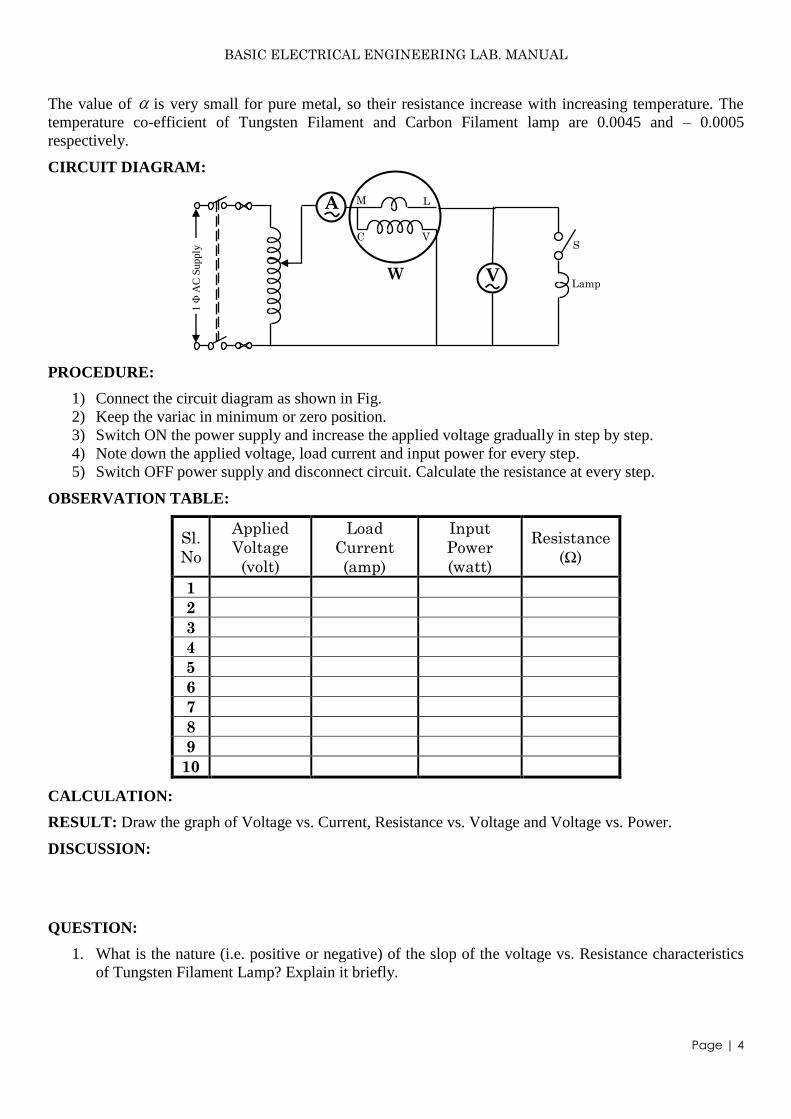
Current fowling through a load resistance LR connected across any two terminal A and B of a
linear, bilateral network is given TH
TH L
V
R R, where
THV is the open circuit voltage or thevenin’s equivalent
voltage (i.e. voltage across terminal AB when LR is removed) and
THR is the by equivalent resistance of the
network as viewed from the open circuited load terminals i.e. from terminal AB deactivating all independent
source.
Mathematically current through the load resistance RL is given by the equation –
THL
TH L
VI
R R
Where, LI
= Load Current
THV
= Open circuit voltage across the terminals AB.
THR = Thevenin’s Resistance
LR = Load Resistance
The following are the limitation of this theorem
i. Thevenin’s theorem cannot be applicable for non-linear network.
ii. This theorem cannot calculate the power consumed internally in the circuit or efficiency of
the circuit.
RL
RTH
VTH
+ A
B
IL
BASIC ELECTRICAL ENGINEERING LAB. MANUAL
Page | 6
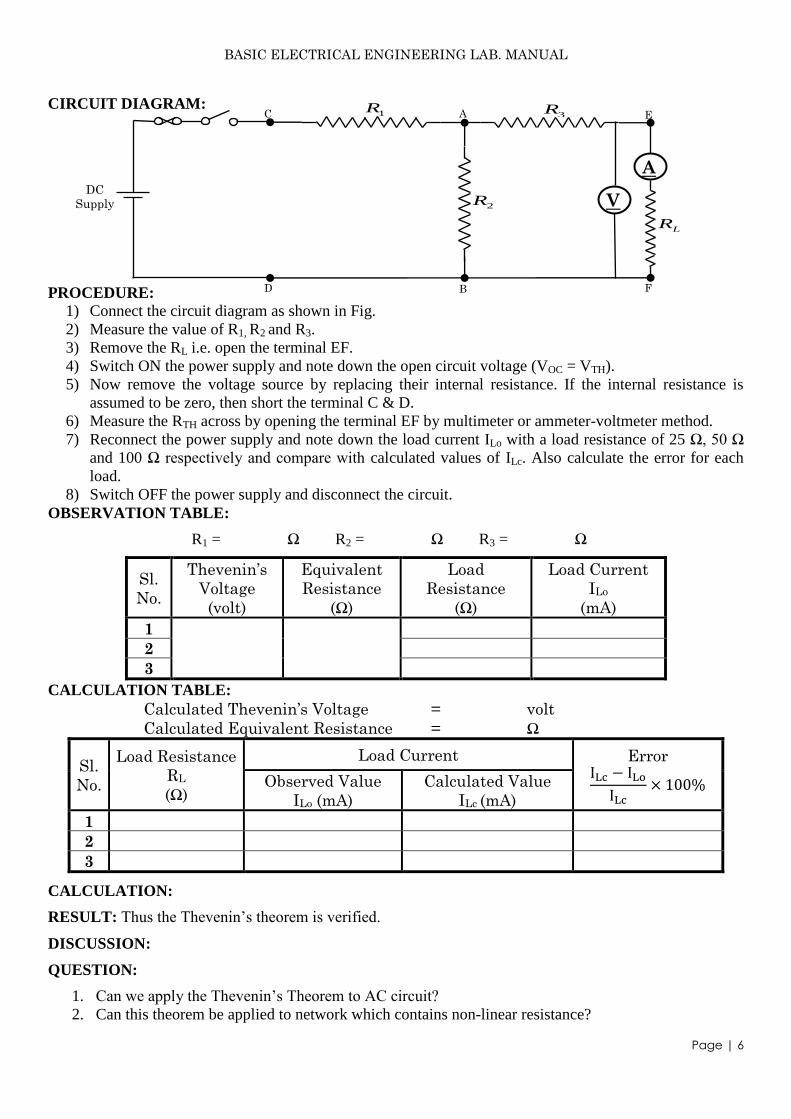
CIRCUIT DIAGRAM:
PROCEDURE:
1) Connect the circuit diagram as shown in Fig.
2) Measure the value of R1, R2 and R3.
3) Remove the RL i.e. open the terminal EF.
4) Switch ON the power supply and note down the open circuit voltage (VOC = VTH).
5) Now remove the voltage source by replacing their internal resistance. If the internal resistance is
assumed to be zero, then short the terminal C & D.
6) Measure the RTH across by opening the terminal EF by multimeter or ammeter-voltmeter method.
7) Reconnect the power supply and note down the load current ILo with a load resistance of 25 Ω, 50 Ω
and 100 Ω respectively and compare with calculated values of ILc. Also calculate the error for each
load.
8) Switch OFF the power supply and disconnect the circuit.
OBSERVATION TABLE:
R1 = Ω R2 = Ω R3 = Ω
Sl.
No.
Thevenin’s
Voltage
(volt)
Equivalent
Resistance
(Ω)
Load
Resistance
(Ω)
Load Current
ILo
(mA)
1
2
3
CALCULATION TABLE:
Calculated Thevenin’s Voltage = volt
Calculated Equivalent Resistance = Ω
Sl.
No.
Load Resistance
RL
(Ω)
Load Current Error
Observed Value
ILo (mA)
Calculated Value
ILc (mA)
1
2
3
CALCULATION:
RESULT: Thus the Thevenin’s theorem is verified.
DISCUSSION:
QUESTION:
1. Can we apply the Thevenin’s Theorem to AC circuit?
2. Can this theorem be applied to network which contains non-linear resistance?
DC
Supply
1R 3R
2R
A
LR
B D F
A C E
V
BASIC ELECTRICAL ENGINEERING LAB. MANUAL
Page | 7
EXPERIMENT NO : 4
TITLE: VERIFICATION OF SUPERPOSITION THEOREM.
OBJECTIVE : To verify the Superposition Theorem in the DC circuit.
APPRATUS :
Sl
No
Apparatus
Name
Apparatus
Type Range
1 Trainer Kit
2 Voltage Source
3 Resistor 1, 2 & 3
4 Ammeter
5 Voltmeter 1
6 Voltmeter 2
7 Multimeter
THEORY:
Superposition Theorem as applied for DC circuit may be stated as:
In any linear active bilateral network containing several sources, the current through or voltage
across any branch in the network equals the algebraic sum of the currents or voltages of each individual
source considered separately with all other sources made inoperative, i.e. replaced by resistance equal to
their internal resistance.
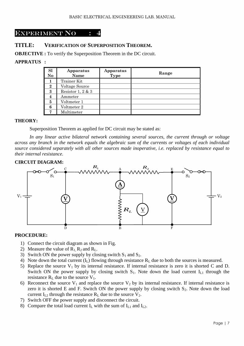
CIRCUIT DIAGRAM:
PROCEDURE:
1) Connect the circuit diagram as shown in Fig.
2) Measure the value of R1, R2 and RL.
3) Switch ON the power supply by closing switch S1 and S2.
4) Note down the total current (IL) flowing through resistance RL due to both the sources is measured.
5) Replace the source V1 by its internal resistance. If internal resistance is zero it is shorted C and D.
Switch ON the power supply by closing switch S1. Note down the load current IL1 through the
resistance RL due to the source V1.
6) Reconnect the source V1 and replace the source V2 by its internal resistance. If internal resistance is
zero it is shorted E and F. Switch ON the power supply by closing switch S2. Note down the load
current IL2 through the resistance RL due to the source V2.
7) Switch OFF the power supply and disconnect the circuit.
8) Compare the total load current IL with the sum of IL1 and IL2.
V1 V V
B D F
A C E 1R 2R
LR
A
V2
S1 S2
V
BASIC ELECTRICAL ENGINEERING LAB. MANUAL
Page | 8
OBSERVATION TABLE:
V1 = volt V2 = volt
R1 = Ω R2 = Ω RL = Ω
Condition
Measured Value (Me)
Load Voltage
(Volt)
Load Current
(mA)
Both V1 and V2 present VL IL
V1 present and V2 replace by internal resistance VL1 IL1
V2 present and V1 replace by internal resistance VL2 IL2
Algebraic Sum VL=VL1+VL2 (IL=IL1+IL2)
CALCULATION TABLE:
Condition
Load Voltage (volt) Error
Measured
Value
Calculated
Value
V1 present and V2 replace by internal
resistance
VL1m VL1c
V2 present and V1 replace by internal
resistance
VL2m VL2c
Both V1 and V2 present (Algebraic Sum) VLm=VL (VLc=VL1c+VL2c)
Condition
Load Current (mA) Error
Measured
Value
Calculated
Value
V1 present and V2 replace by internal resistance IL1m IL1c
V2 present and V1 replace by internal resistance IL2m IL2c
Both V1 and V2 present (Algebraic Sum) ILm=IL (ILc=IL1c+IL2c)
CALCULATION:
RESULT: Thus the Superposition theorem is verified.
DISCUSSION:
QUESTION:
1. Can we apply the Superposition Theorem to AC circuit?
2. Does non-linear system obey the superposition theorem? Explain it.
BASIC ELECTRICAL ENGINEERING LAB. MANUAL
Page | 9
EXPERIMENT NO : 5
TITLE: STUDY THE RLC SERIES CIRCUIT.
OBJECTIVE : To study the RLC series circuit and draw the following characteristics
I. Frequency vs. Resistance
II. Frequency vs. Impedance
III. Frequency vs. Inductive reactance
IV. Frequency vs. Capacitive reactance
V. Frequency vs. Current
APPRATUS :
Sl
No
Apparatus
Name
Apparatus
Type Range
1 Resistor
2 Inductor
3 Capacitor
4 Voltmeter
5 Audio Frequency
Generator
THEORY:
Consider an AC circuit containing resistance R, inductor L and a capacitor C connected in series as
shown in figure below
The Impedance 22 2 2
L CZ R X R X X
Where 2LX fL and 1
2CX
fC .
At resonance L CX X i.e.
L CX X = 0. Therefore impedance of the circuit is R i.e. Z R . So,
current flowing through the circuit is maximum, given byV
IR
. In that condition voltage drop across the
inductor and voltage drop across the capacitor is same and the power factor is unity. When these conditions
are exists, the circuit is said to be in resonance. The frequency at which this occurs is called Resonance
frequency, rf .
At resonance L CX X
So 1
r
r
LC
2 1r
LC
1r
LC
R
A
L C
BASIC ELECTRICAL ENGINEERING LAB. MANUAL
Page | 10
Therefore resonance frequency, 1
2rf
LC . Hence, the value of resonance frequency depends on
the parameter of the two energy storing elements.
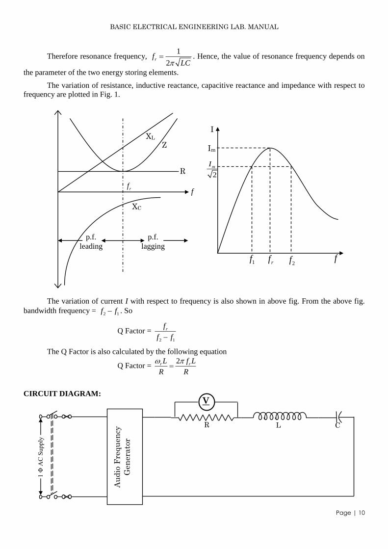
The variation of resistance, inductive reactance, capacitive reactance and impedance with respect to
frequency are plotted in Fig. 1.
The variation of current I with respect to frequency is also shown in above fig. From the above fig.
bandwidth frequency = 2 1f f . So
Q Factor = 2 1
rf
f f
The Q Factor is also calculated by the following equation
Q Factor = 2r rL f L
R R
CIRCUIT DIAGRAM:
I
Im
2
mI
rf 2f 1f f
rff
R
XL
Z
XC
p.f.
lagging
p.f.
leading
V
R L C
1 Φ
AC
Su
pp
ly
Au
dio
Fre
qu
en
cy
Gen
era
tor
BASIC ELECTRICAL ENGINEERING LAB. MANUAL
Page | 11
PROCEDURE:
1) Connect the circuit diagram as shown in Fig.
2) Switch ON the power supply.
3) Vary the frequency step by step in small steps by adjust frequency variation knob.
4) Note down the voltmeter reading which indicate voltage across the resistance.
5) Switch OFF the power supply and disconnect the circuit.
OBSERVATION TABLE:
Sl. No
Frequency f
(Hz)
Resistance R
(Ω)
Inductance L
(mH)
Inductive Reactance
XL (Ω)
Capacitance C
(µF)
Capacitive Reactance
XC (Ω)
Impedance
Z (Ω)
Voltage
across R VR
(volt)
Current I = VR/R
(amp)
1
2
3
4
5
6
7
8
9
10
11
12
13
14
15
16
17
18
19
20
CALCULATION:
RESULT: Calculate resonance frequency, bandwidth and Q – factor. Also draw the following
characteristics
I. Frequency vs. Resistance
II. Frequency vs. Impedance
III. Frequency vs. Inductive reactance
IV. Frequency vs. Capacitive reactance
V. Frequency vs. Current
DISCUSSION :
QUESTION:
1. What is resonance? State the resonance condition for series RLC circuit.
2. Define Band Width and Q – factor.
3. Draw the phasor diagram for series RLC circuit.
BASIC ELECTRICAL ENGINEERING LAB. MANUAL
Page | 12
EXPERIMENT NO : 67
TITLE: SPEED CONTROL OF DC SHUNT MOTOR
OBJECTIVE : To study the speed control of a DC shunt motor using
A. Field current control
B. Armature voltage control
APPARATUS:
Sl
No
Apparatus
Name
Apparatus
Type Range/ Specification
1 DC Motor
2 Ammeter
3 Voltmeter
4 Rheostat
5 Tachometer
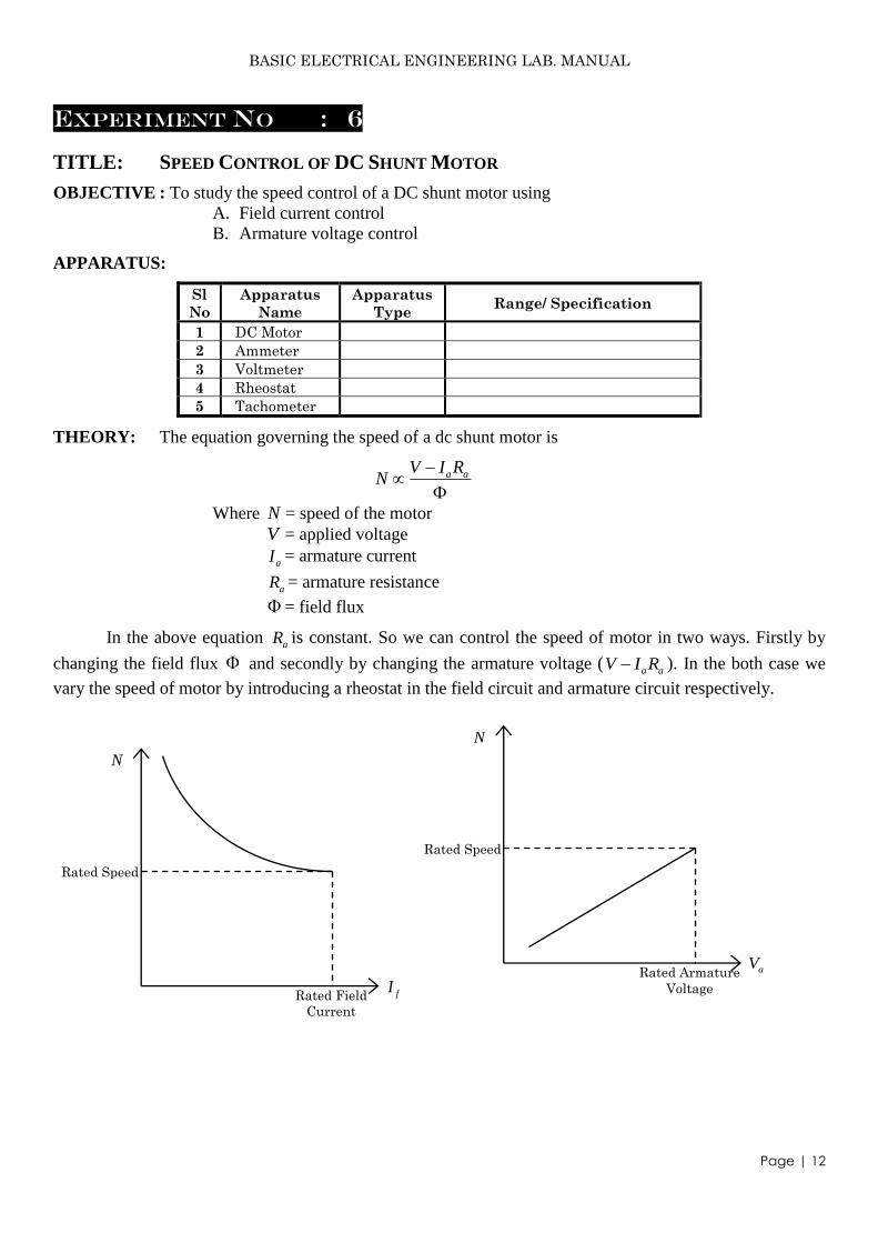
THEORY: The equation governing the speed of a dc shunt motor is
a aV I RN
Where N = speed of the motor
V = applied voltage
aI = armature current
aR = armature resistance
= field flux
In the above equation aR is constant. So we can control the speed of motor in two ways. Firstly by
changing the field flux and secondly by changing the armature voltage (a aV I R ). In the both case we
vary the speed of motor by introducing a rheostat in the field circuit and armature circuit respectively.
N
fI
Rated Speed
Rated Field
Current
N
aV
Rated Speed
Rated Armature
Voltage
BASIC ELECTRICAL ENGINEERING LAB. MANUAL
Page | 13
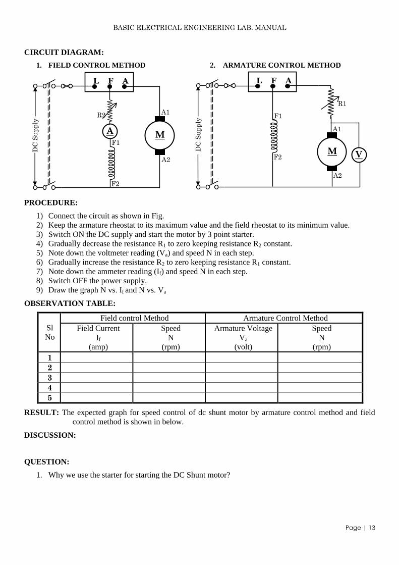
CIRCUIT DIAGRAM:
1. FIELD CONTROL METHOD 2. ARMATURE CONTROL METHOD
PROCEDURE:
1) Connect the circuit as shown in Fig.
2) Keep the armature rheostat to its maximum value and the field rheostat to its minimum value.
3) Switch ON the DC supply and start the motor by 3 point starter.
4) Gradually decrease the resistance R1 to zero keeping resistance R2 constant.
5) Note down the voltmeter reading (Va) and speed N in each step.
6) Gradually increase the resistance R2 to zero keeping resistance R1 constant.
7) Note down the ammeter reading (If) and speed N in each step.
8) Switch OFF the power supply.
9) Draw the graph N vs. If and N vs. Va
OBSERVATION TABLE:
Sl
No
Field control Method Armature Control Method
Field Current
If
(amp)
Speed
N
(rpm)
Armature Voltage
Va
(volt)
Speed
N
(rpm)
1
2
3
4
5
RESULT: The expected graph for speed control of dc shunt motor by armature control method and field
control method is shown in below.
DISCUSSION:
QUESTION:
1. Why we use the starter for starting the DC Shunt motor?
F1
F2
A
DC
Su
pp
ly
L F A
M
A1
A2
R2
R1
DC
Su
pp
ly
L F A
F1
F2 V
A2
M
A1
BASIC ELECTRICAL ENGINEERING LAB. MANUAL
Page | 14
EXPERIMENT NO : 7
TITLE: STUDY OF THE EQUIVALENT CIRCUIT OF A SINGLE-PHASE TRANSFORMER.
OBJECTIVE : To determine the parameter of the equivalent circuit of a single phase transformer
APPRATUS :
Sl
No
Apparatus
Name
Apparatus
Type Range/Specification
1 Transformer
2 Ammeter
3 Voltmeter
4 Wattmeter
5 Variac
THEORY:
1. OPEN CIRCUIT (OC) OR NO-LOAD TEST
The purpose of this test is to determine the shunt branches parameter of the equivalent circuit of the
transformer. This test is performed in LV side which is connected to rated supply voltage at rated frequency
and HV side is kept open as shown in fig. The exciting current being about 2 to 6 % of full load current and
the ohmic loss in the primary i.e. LV side varies from 0.04 % to 0.36 % of full load ohmic loss. In view of
this ohmic loss during open circuit test is negligible in comparison with the core loss. Hence the wattmeter
reading can taken as equal to transformer core loss.
Let consider oV = Applied voltage on low voltage side
oI = Exciting current or No-load current
oP = Core loss
Then coso o o oP V I
Therefore no load power factor cos oo
o o
P
V I
The energy component of no load current cose o oI I
The magnetizing component of no load current sinm o oI I
Therefore core loss resistance oo
e
VR
I
And magnetizing reactance oo
m
VX
I
2. SHORT CIRCUIT (SC) TEST
This test is performed to determine the series parameter of equivalent circuit of transformer as well
as to obtain the full load copper loss of a single phase transformer. The LV side of the transformer is short
circuited and the instruments are placed in HV side. The applied voltage is varied by variac to supply the
rated current on HV side. As the primary mmf is almost equal to the secondary mmf in transformer,
therefore rated current in high voltage winding cause the flow of rated current in low voltage winding. The
wattmeter, in short circuit test, records the core loss and ohmic loss in both the winding. Since the core loss
has been also negligible in comparison with rated voltage core loss, wattmeter reading can taken as equal to
transformer ohmic loss in both winding.
Let consider scV = Applied voltage on high voltage side
scI = Short circuit current on high voltage side
BASIC ELECTRICAL ENGINEERING LAB. MANUAL
Page | 15
scP = Total ohmic loss
Then the total equivalent resistance referred to high voltage side 2
sceq
sc
PR
I
The total equivalent impedance referred to high voltage side sceq
sc
VZ
I
Therefore the total equivalent reactance referred to high voltage side 2 2
eq eq eqX Z R
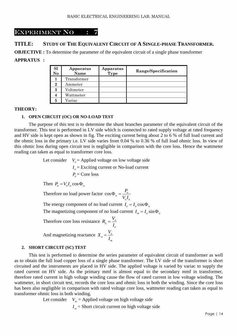
CIRCUIT DIAGRAM:
1. OPEN CIRCUIT TEST
Fig. (a) 2. SHORT CIRCUIT TEST
Fig. (b)
PROCEDURE :
1) Connect the circuit as shown in Fig (a)
2) Set the variac at zero output voltage.
3) Switch ON the supply and by varying the applied voltage in step from zero to rated voltage of low
voltage (LV) side.
4) Note down the ammeter, voltmeter and wattmeter reading.
5) Disconnect the circuit from supply and again connect the circuit as shown in Fig (b)
6) Set the variac at zero output voltage.
7) Switch ON the supply and increase the input voltage of transformer starting from zero in varying
small step till ammeter indicates the full load current of high voltage (HV) side.
8) Note down the ammeter, voltmeter and wattmeter reading.
9) Disconnect the circuit from supply.
10) Calculate the different parameter of transformer from the record data.
11) Draw the equivalent circuit of single phase transformer.
A
V
M
C V
L
W
1 Φ
AC
Su
pp
ly
1 Φ
AC
Su
pp
ly
M
C V
L
W V
A
HV LV
LV HV
BASIC ELECTRICAL ENGINEERING LAB. MANUAL
Page | 16
OBSERVATION TABLE:
Open Circuit Test Short Circuit Test
Voltage
Vo
(volt)
Current
Io
(Amp)
Power Input
Po
(watt)
Voltage
Vsc
(volt)
Current
Isc
(Amp)
Power Input
Psc
(watt)
CALCULATION:
RESULT: Core loss resistance, Ro = ohm
Magnetizing reactance, Xo = ohm
Total equivalent resistance referred to high voltage side, Req = ohm
Total equivalent reactance referred to high voltage side, Xeq = ohm
DISCUSSION:
QUESTION:
1. Draw the equivalent circuit diagram of single phase transformer.
BASIC ELECTRICAL ENGINEERING LAB. MANUAL
Page | 17
EXPERIMENT NO : 8
TITLE: VERIFICATION OF NORTON’S THEOREM.
OBJECTIVE : To verify the Norton’s Theorem in the DC circuit.
APPRATUS:
Sl
No
Apparatus
Name
Apparatus
Type Range
1 Trainer Kit
2 Voltage Source
3 Resistor 1,2,3 & 4
4 Ammeter
5 Multimeter
THEORY:
Norton’s Theorem as applied for DC circuit may be stated as:
Any two terminal linear, active, bilateral networks containing voltage source and resistance when
viewed from its output terminals is equivalent to a constant current source and a parallel connected
equivalent resistance. The constant current source (Norton’s equivalent current source) is of magnitude of
the short circuit current at the terminals. The internal resistance is equivalent resistance of the network
looking back into the terminal with all the sources replaced by their internal resistance.
Mathematically, current through the load resistance RL is given by the equation
NL SC
N L
RI I
R R
Where, LI
= Load Current
NR = Norton’s Resistance
SCI
= Short circuit current across the terminals.
LR = Load Resistance
CIRCUIT DIAGRAM:
IL
A
B
RL RN ISC
1R 3R
DC
Supply
B D F
A C E
2R
A
LR
4R
BASIC ELECTRICAL ENGINEERING LAB. MANUAL
Page | 18
PROCEDURE:
1) Connect the circuit diagram as shown in Fig.
2) Measure the value of R1, R2, R3 and R4.
3) Remove the RL and short the line.
4) Switch ON the power supply and note down ammeter reading as short circuit current (ISC = IN).
5) Now remove the voltage source by replacing their internal resistance. If the internal resistance is
assumed to be zero, then short the terminal C & D.
6) Measure the RN across by opening the terminal EF by multimeter or ammeter-voltmeter method.
7) Note down the load current ILo with a load resistance of 25 Ω, 50 Ω and 100 Ω respectively and
compare with calculated values of ILc. Also calculate the error for each load.
8) Switch OFF the power supply and disconnect the circuit.
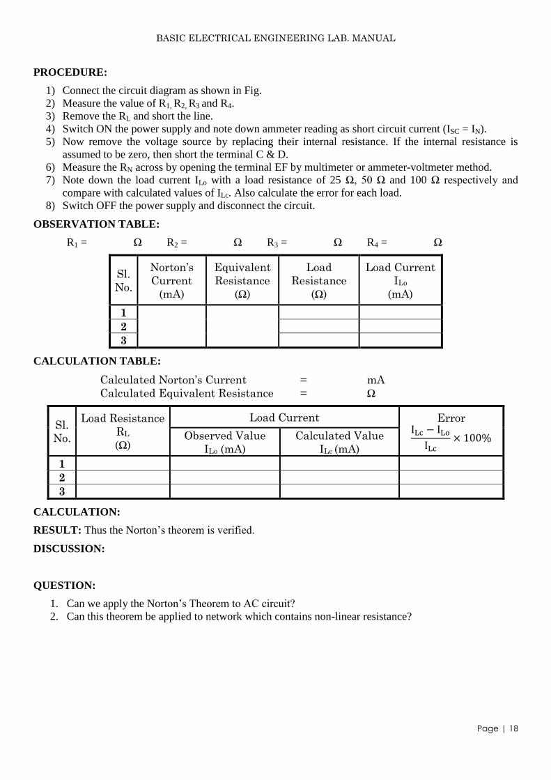
OBSERVATION TABLE:
R1 = Ω R2 = Ω R3 = Ω R4 = Ω
Sl.
No.
Norton’s
Current
(mA)
Equivalent
Resistance
(Ω)
Load
Resistance
(Ω)
Load Current
ILo
(mA)
1
2
3
CALCULATION TABLE:
Calculated Norton’s Current = mA
Calculated Equivalent Resistance = Ω
Sl.
No.
Load Resistance
RL
(Ω)
Load Current Error
Observed Value
ILo (mA)
Calculated Value
ILc (mA)
1
2
3
CALCULATION:
RESULT: Thus the Norton’s theorem is verified.
DISCUSSION:
QUESTION:
1. Can we apply the Norton’s Theorem to AC circuit?
2. Can this theorem be applied to network which contains non-linear resistance?
BASIC ELECTRICAL ENGINEERING LAB. MANUAL
Page | 19
EXPERIMENT NO : 9
TILLE: CALIBRATION OF MI TYPE AMMETER AND VOLTMETER
OBJECTIVE : To calibrate MI type ammeter and voltmeter with a standard(PMMC) ammeter and
voltmeter.
APPARATUS:
Sl
No
Apparatus
Name
Apparatus
Type
Quantity Range
1 Variac
2 MI Ammeter
3 PMMC Ammeter
4 MI Voltmeter
5 PMMC
Voltmeter
6 Load Box
THEORY:
The calibration of all instruments is important since it affords the opportunity to check the instrument
against a known standard and subsequently to find errors and accuracy. Calibration procedures involve a
comparison of the particular instrument with either (1) a primary standard, (2) a secondary standard with a
higher accuracy than the instrument to be calibrated, or (3) an instrument of known accuracy. So all working
instrument must be calibrated against some reference instruments, which have higher accuracy.
Permanent-magnet moving coil type instrument can be used for direct current measurements only but
moving iron instruments can be used for both AC and DC quantity measurement. Although, the moving iron
instruments are responsive to DC, the hysteresis effect causes an appreciable error in measurement. But the
permanent magnet moving coil instrument is the most accurate type for direct current measurement. So it is
important to know the error in the reading of moving iron voltmeter and ammeter when the DC voltage or
current is measured in any circuit.
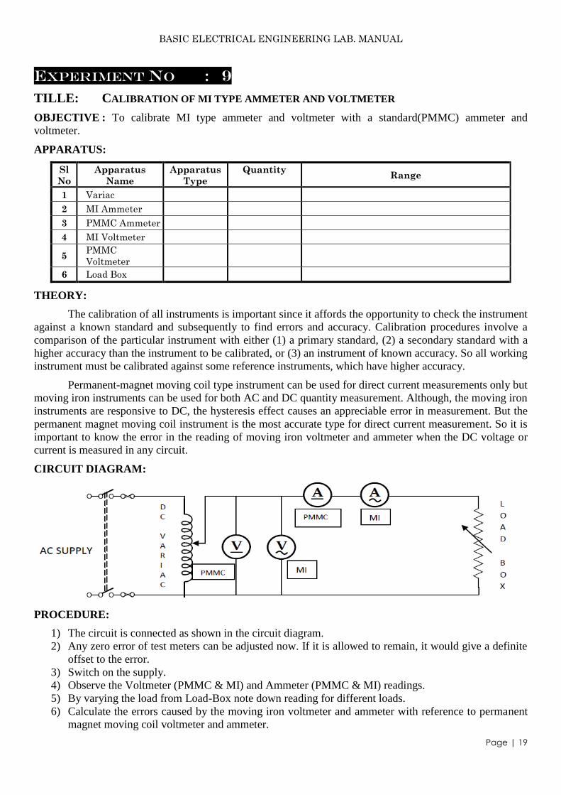
CIRCUIT DIAGRAM:
PROCEDURE:
1) The circuit is connected as shown in the circuit diagram.
2) Any zero error of test meters can be adjusted now. If it is allowed to remain, it would give a definite
offset to the error.
3) Switch on the supply.
4) Observe the Voltmeter (PMMC & MI) and Ammeter (PMMC & MI) readings.
5) By varying the load from Load-Box note down reading for different loads.
6) Calculate the errors caused by the moving iron voltmeter and ammeter with reference to permanent
magnet moving coil voltmeter and ammeter.
BASIC ELECTRICAL ENGINEERING LAB. MANUAL
Page | 20
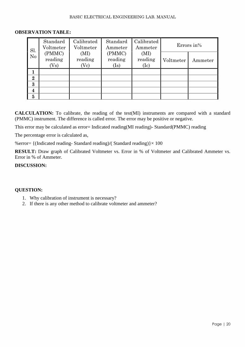
OBSERVATION TABLE:
Sl.
No
Standard
Voltmeter
(PMMC)
reading
(Vs)
Calibrated
Voltmeter
(MI)
reading
(Vc)
Standard
Ammeter
(PMMC)
reading
(Is)
Calibrated
Ammeter
(MI)
reading
(Ic)
Errors in%
Voltmeter Ammeter
1
2
3
4
5
CALCULATION: To calibrate, the reading of the test(MI) instruments are compared with a standard
(PMMC) instrument. The difference is called error. The error may be positive or negative.
This error may be calculated as error= Indicated reading(MI reading)- Standard(PMMC) reading
The percentage error is calculated as,
%error= (Indicated reading- Standard reading)/( Standard reading)× 100
RESULT: Draw graph of Calibrated Voltmeter vs. Error in % of Voltmeter and Calibrated Ammeter vs.
Error in % of Ammeter.
DISCUSSION:
QUESTION:
1. Why calibration of instrument is necessary?
2. If there is any other method to calibrate voltmeter and ammeter?