Embed Size (px)
Citation preview
Time-Interleaved High-speed
D/A Converters
Erik Olieman
Samenstelling promotiecommissie:
Voorzitter en secretaris: Prof.dr. P.M.G. Apers Universiteit Twente Promotor: Prof.dr.ir B. Nauta Universiteit Twente Assistent-promotor: Dr.ir. A.J. Annema Universiteit Twente Leden: Prof.dr. K.A.A. Makinwa Technische Universiteit Delft Prof.dr.ir. F.E. van Vliet Universiteit Twente Prof.ir. A.J.M. van Tuijl Universiteit Twente Prof.dr.ir. K. Doris Technische Universiteit Eindhoven
This research is conducted as part of the Sensor Technology Applied in Reconfigurable systems for sustainable Security (STARS) project, see also www.starsproject.nl.
Centre for Telematics and Information Technology P.O. Box 217, 7500 AE Enschede, The Netherlands
ISBN: 978-90-365-4019-3 DOI: http://dx.doi.org/10.3990/1.9789036540193 Copyright © 2015 by Erik Olieman, Enschede, The Netherlands
TIME-INTERLEAVED HIGH-
SPEED D/A CONVERTERS
PROEFSCHRIFT
Ter verkrijging van de graad van doctor aan de Universiteit Twente,
op gezag van de rector magnificus, prof. dr. H. Brinksma,
volgens besluit van het College voor Promoties in het openbaar te verdedigen
op woensdag 2 maart 2016 om 14:45
door
Erik Olieman geboren op 28 mei 1989
te Wageningen

Dit proefschrift is goedgekeurd door:
De promotor: Prof. dr. Ir. Bram Nauta
De assistent-promotor: Dr.ir. A.J. Annema
i
Samenvatting
Het onderwerp van deze scriptie zijn energie efficiënte, snelle digitaal-naar-analoog
converters (DACs) in CMOS technologie, die de mogelijkheid bieden om signalen van
DC tot RF te genereren. Tegenwoordig worden componenten in RF ketens bij voorkeur
in het digitale domein geplaatst in plaats van in het analoge domein. Dit levert
voordelen op qua flexibiliteit en betere prestaties bij nieuwere CMOS technologieën.
Welke taken naar het digitale domein kunnen worden verplaatst hangt, voor een
significant gedeelte, af van de prestaties van de aanwezige DACs.
Het werk aan deze scriptie was onderdeel van het STARS project, wat als doel heeft om
technologieën voor re-configureerbare radar systemen te ontwikkelen. De
mogelijkheid om meer taken in het digitale domein uit te voeren, wat kan wanneer
betere DACs ontwikkeld worden, past goed bij de doelen van het STARS project.
De meest gebruikte DAC techniek voor generatie van hoog frequente signalen is de
stroom-sturende DAC. De werking en de beperkingen van dit type DAC wordt
besproken in deze thesis, inclusief een aantal bekende oplossingen uit de literatuur
voor de beperkingen van deze DACs. Er wordt aangetoond dat de primaire fout-
mechanismes plaatsvinden op, of direct na, het moment waarbij er naar nieuwe data
wordt geschakeld. Voor de rest van de periode van de DAC, zodra de uitgang zijn
definitieve waarde heeft aangenomen, is de uitgang nagenoeg ideaal. Deze fouten
gerelateerd aan het schakelgedrag van DAC beperken de te behalen bandbreedte en
energie efficiëntie van conventionele DACs.
Interleaved stroom-sturende DACs, het onderwerp van deze thesis, worden
geïntroduceerd om de beperkingen in nauwkeurigheid door schakel fouten te
onderdrukken. Interleaved DACs bestaan uit twee sub-DACs die parallel hun werk
doen, en door een analoge multiplexer gecombineerd worden tot één uitgang. De
sDACs zijn standaard stroom-sturende DACs, die door hun niet-ideale gedrag een
beperkte nauwkeurigheid hebben. Nadat één van de sDACs een nieuwe digitale code
ii
krijgt om te converteren, krijgt hij in de interleaved DAC wat tijd om naar zijn definitieve
waarde te convergeren. Gedurende deze periode is de andere sDAC, die op de
tegenovergestelde fase van de klok werkt, verbonden met de uitgang via de analoge
multiplexer. Zodra de eerste sDAC zijn definitieve waarde heeft bereikt, schakelt de
analoge multiplexer en wordt deze eerste sDAC met de uitgang verbonden.
Ondertussen krijgt de tweede sDAC een nieuwe digitale code, en krijgt die tijd om naar
zijn uiteindelijke waarde te convergeren. Deze architectuur isoleert de dominante
fouten van de sDACs, die rond het schakelmoment optreden, van de daadwerkelijke
uitgang.
De interleaved architectuur resulteert in een hogere lineariteit van hoge-snelheids
DACs, echter er zijn ook een aantal beperkingen waar rekening mee gehouden moet
worden. De analoge multiplexer moet voldoende lineair zijn, de amplitude van de twee
sDACs moet soortgelijk zijn, en ook de duty cycle van de twee sDACs moet nauwkeurig
gedefinieerd zijn. Zoals beschreven in hoofdstuk 3, het gedrag van de analoge
multiplexer is code-onafhankelijk door gebruik te maken van triode schakelaars in
plaats van saturatie schakelaars. Daarnaast wordt er ook een methode geïntroduceerd
in dit hoofdstuk die de fout in de duty cycle kan bepalen en met alleen DC
vergelijkingen.
Om de effectiviteit van de interleaved architectuur aan te tonen is er een 1.7GS/s, 12-
bit DAC ontworpen die een SFDR van meer dan 58dB heeft over zijn complete Nyquist
bandbreedte, en hierbij 70mW nodig heeft. De individuele stroombronnen van de
sDACs kunnen worden gekalibreerd met een nieuwe methode waarbij enkel DC
vergelijkingen nodig zijn. De initiële ongekalibreerde fout in de uitgangsamplitudes van
de sDACs is 60LSB, terwijl na kalibratie dit met een factor 150 is gereduceerd tot slechts
0.4LSB. Een digitaal gestuurde condensator bank is aanwezig op de chip om de duty
cycle aan te kunnen passen. Derde orde intermodulatie producten zijn met bijna 20dB
onderdrukt in de interleaved uitgang ten opzichte van de uitgang van de sDACs.
Hiernaast zijn nog twee ICs ontworpen. Beide hebben 9-bit resolutie, en meer dan 50dB
SFDR over hun Nyquist bandbreedte terwijl ze 100mW verbruiken. De eerste is
ontworpen en geproduceerd in 65nm CMOS, en werkt op een snelheid van 8.8GS/s,
terwijl de tweede werkt op 11GS/s en in 28nm FDSOI is gemaakt. Beide DACs zijn erg
klein, ze nemen respectievelijk 0.074mm2 en 0.04mm2 in. Deze efficiëntie is bereikt
door gebruik te maken van quad-switching, waarmee ongewenste code-afhankelijke

iii
effecten verder onderdrukt worden. De duty cycle van deze DACs kan aangepast
worden door een externe spanning aan te bieden.
Deze drie chips tonen aan dat, ondanks dat er twee sDACs nodig zijn, de interleaved
architectuur erg geschikt is voor het ontwerpen van kleine, zuinige, DACs met goede
performance bij hele hoge snelheden.


v
Abstract
This thesis is on power efficient very high-speed digital-to-analog converters (DACs) in
CMOS technology, intended to generate signals from DC to RF. Components in RF signal
chains are nowadays often moved from the analog domain to the digital domain. This
allows for more flexibility and better scaling of performance with new CMOS processes.
The number of tasks in the transmit chain that can be moved to the digital domain
depends on the performance of the available DACs.
This thesis was performed as part of the STARS project, which is intended to develop
the technologies required for reconfigurable radar systems. The flexibility and
reconfigurability which is possible in the digital domain fits well within the scope of the
project, which can be better exploited with improved DACs.
The most widely used DAC implementation for high-speed operation is the current
steering DAC. Its operating principles and its limitations are discussed in the
introduction of this thesis, including some solutions reported in literature for these
limitations. It is shown that the major error sources of conventional high-speed current
steering DACs occur right at or after the switching instance, while for the majority of
the DAC’s period, after its output is settled, the output is close to ideal. These switching
related errors limit the signal frequency range and power efficiency of conventional
DACs considerably.
Interleaved current steering DACs, which are the topic of this thesis, are introduced to
circumvent these performance-limiting switching related issues. The interleaved
architecture consists of two sub-DACs that operate in parallel and an analog multiplexer
that combines them into one output. The sDACs are regular current steering DACs, with
limited performance due to their non-ideal behavior. After one of the sDACs is supplied
with a new digital code, it gets some time to settle. During this time the other sDAC
which operates at the opposite clock phase is connected to the output via the analog
multiplexer. After the first sDAC is finished settling, the analog multiplexer toggles and

vi
connects that sDAC to the output. Meanwhile the second sDAC is supplied with a new
digital code and gets time to settle its output. This architecture isolates the most
dominant errors of the sDACs, which are centered around the switching instance, from
the actual output.
This interleaved architecture allows for better linearity for high-speed DACs, but it also
has some inherent limitations that need to be taken into account. The analog
multiplexer should be sufficiently linear, the full scale amplitude of the sDACs need to
be similar, and also the duty cycle of the two sDACs need to be accurately defined. As
described in chapter 3, code independent behavior of the analog multiplexer is
achieved by employing triode switches instead of saturation switches. Also a method
to measure the duty cycle error is introduced which only requires DC comparisons.
In order to proof the viability of the interleaved architecture a 1.7GS/s, 12-bit DAC is
designed that achieves better than 58dB SFDR over Nyquist while consuming 70mW.
The individual current sources of the sDACs can be calibrated with a new method using
only DC comparisons. The initial uncalibrated gain error between the two sDACs is over
60LSB, while after calibration this is reduced by a factor 150 to only 0.4LSB. A digital
capacitor bank is included which is capable of adjusting the duty cycle to remove any
duty cycle associated errors. The third order intermodulation products are reduced by
almost 20dB when the interleaved output is compared to the direct output of the
sDACs.
Two more ICs are designed, both having 9-bit resolution, better than 50dB SFDR over
Nyquist and close to 100mW power consumption. The first one is produced in 65nm
CMOS and runs at 8.8GS/s, while the second one runs at 11GS/s and is produced in
28nm FDSOI. Their core area is very small: they occupy respectively 0.074mm2 and
0.04mm2. This power efficient high-speed operation is achieved by using quad-
switching to further suppress unwanted code-dependent behavior. Their duty cycle can
be adjusted using external tune voltages.
All these demonstrator ICs show that despite requiring two separate sDACs, the
introduced interleaved architecture is very suitable to design small, low-power DACs
with good performance at very high sample rates.
vii
Contents
Samenvatting .............................................................................................................. i
Abstract ..................................................................................................................... v
Introduction ....................................................................................................... 1
1.1 STARS ............................................................................................................ 2
Analog and Digital Performance ................................................................ 4
1.2 Waveforms for Radar Applications .............................................................. 5
Linearity Implementations ......................................................................... 5
Phase Noise ................................................................................................ 7
Quantization noise ..................................................................................... 8
1.3 DAC Performance Figures ............................................................................. 9
Linearity ..................................................................................................... 9
Sample Rate and Bandwidth .................................................................... 11
Power Consumption and Area ................................................................. 11
Figures-of-Merit ....................................................................................... 12
1.4 DAC architectures ....................................................................................... 15
Charge-Redistribution DAC ...................................................................... 15
R-2R Ladder DAC ...................................................................................... 17
Resistor-String DAC .................................................................................. 18
Current steering DAC ............................................................................... 19
Summary .................................................................................................. 20
1.5 Thesis Outline ............................................................................................. 20
The Current Steering DAC ................................................................................ 23
2.1 Static error mechanisms ............................................................................. 24
Output resistance .................................................................................... 24
viii
Output current variations ........................................................................ 26
2.2 Dynamic mechanisms ................................................................................. 26
2.3 Recent Literature ........................................................................................ 27
Extra Cascodes with Bleeding Current Sources ....................................... 27
Return-to-Zero Switching ......................................................................... 28
Quad-Switching ........................................................................................ 29
Interleaved DACs ..................................................................................... 30
Other publications ................................................................................... 31
The Interleaved Structure ................................................................................ 33
3.1 Interleaving errors mechanisms ................................................................. 35
Static matching of the sDACs ................................................................... 36
Dynamic matching of the multiplexer ..................................................... 39
Multiplexer transistor nonlinearities ....................................................... 41
3.2 Measuring duty cycle.................................................................................. 43
Medium Speed Demonstrator: 12-bits at 1.7GS/s .......................................... 45
4.1 Architecture ................................................................................................ 45
Static matching ........................................................................................ 46
Dynamic matching ................................................................................... 47
4.2 Circuit implementation details ................................................................... 47
Multiplexer and driver design .................................................................. 48
Bias design ............................................................................................... 48
Digital circuitry ......................................................................................... 51
4.3 Measurement results ................................................................................. 53
Static matching ........................................................................................ 53
Dynamic matching ................................................................................... 55
Spectrum .................................................................................................. 55
Low voltage operation ............................................................................. 57
Comparison to state-of-the-art ............................................................... 58
4.4 Conclusions ................................................................................................. 59
High-speed Demonstrator: 9-bits at 8.8GS/s and 11GS/s ............................... 61
5.1 Suppressing code-dependent supply and bias load: Quad-switching ........ 62
5.2 Circuit implementation details ................................................................... 64
Current sources ........................................................................................ 65

ix
Switch drivers and signal generation ....................................................... 66
Multiplexer and driver design .................................................................. 67
5.3 Demonstrator chip ..................................................................................... 69
5.4 Measurements ........................................................................................... 71
Comparison to state-of-the-art ............................................................... 75
5.5 Conclusions ................................................................................................. 75
Conclusions ...................................................................................................... 77
6.1 Summary and conclusions .......................................................................... 77
6.2 Future work ................................................................................................ 78
Signal swing .............................................................................................. 79
Background timing calibration ................................................................. 81
A Co-existing timing and amplitude errors ......................................................... 83
B On-chip memory architecture ......................................................................... 87
Basic architecture ....................................................................................... 87
Memory implementation ........................................................................... 88
Programming the memory ......................................................................... 89
C Layout considerations regarding symmetry .................................................... 93
Problem definition ...................................................................................... 93
Analysis ....................................................................................................... 95
Solution....................................................................................................... 95
D FDSOI for Current steering DACs ..................................................................... 97
Drain to bulk junction ................................................................................. 98
Output resistance ....................................................................................... 98
Matching ..................................................................................................... 98
Dankwoord ..............................................................................................................99
Bibliography ...........................................................................................................101
List of Publications .................................................................................................107
List of Abbreviations ..............................................................................................109

1
Introduction
A digital-to-analog converter (DAC) is a device that converts digital data into an analog
signal. For electronic circuits the analog signal is typically in the form of current, voltage
or charge.
The digital data represents a signal that is both time and amplitude discrete, while
analog signals are both time and amplitude continuous1. The spectrum of the digital
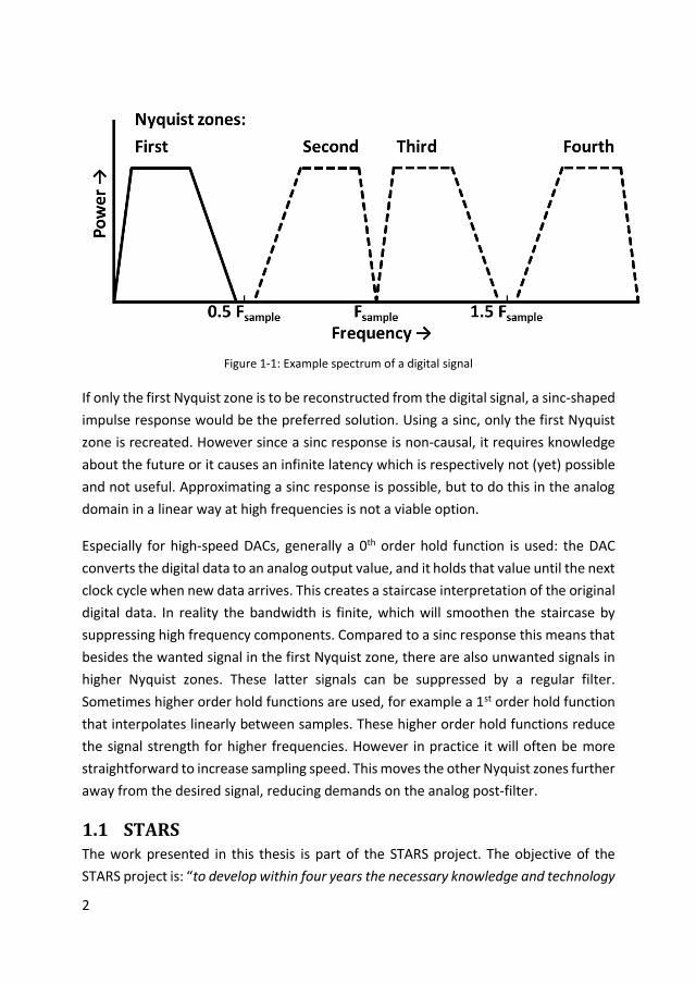
signal is an infinitely repeating copy of the first Nyquist zone, illustrated by figure 1-1.
This can be reproduced in the analog domain by using a (continuous time) impulse
function to reconstruct the digital signal. The first problem with this is that it is not
possible to make an ideal impulse: even implementing an approximation is quite hard.
The other reason not to use ideal(ish) impulse shapes is that generally only the first
Nyquist zone is of interest: recreating other Nyquist zones is counterproductive if only
the first is relevant.
This desired first Nyquist zone is located between DC and half the sample rate, the
Nyquist frequency. Sometimes DACs are used in sub-sampling mode, and a higher zone
is used, however this is rare and in this thesis the focus is on regular DACs which are
intended to create signals in the first Nyquist zone.
1 Fundamentally, for example in a charge based DAC the amount of charge is a discrete number of charge carriers, while also time might be regarded as discrete. For our requirements however we can treat both as continuous.
2
Figure 1-1: Example spectrum of a digital signal
If only the first Nyquist zone is to be reconstructed from the digital signal, a sinc-shaped
impulse response would be the preferred solution. Using a sinc, only the first Nyquist
zone is recreated. However since a sinc response is non-causal, it requires knowledge
about the future or it causes an infinite latency which is respectively not (yet) possible
and not useful. Approximating a sinc response is possible, but to do this in the analog
domain in a linear way at high frequencies is not a viable option.
Especially for high-speed DACs, generally a 0th order hold function is used: the DAC
converts the digital data to an analog output value, and it holds that value until the next
clock cycle when new data arrives. This creates a staircase interpretation of the original
digital data. In reality the bandwidth is finite, which will smoothen the staircase by
suppressing high frequency components. Compared to a sinc response this means that
besides the wanted signal in the first Nyquist zone, there are also unwanted signals in
higher Nyquist zones. These latter signals can be suppressed by a regular filter.
Sometimes higher order hold functions are used, for example a 1st order hold function
that interpolates linearly between samples. These higher order hold functions reduce
the signal strength for higher frequencies. However in practice it will often be more
straightforward to increase sampling speed. This moves the other Nyquist zones further
away from the desired signal, reducing demands on the analog post-filter.
1.1 STARS The work presented in this thesis is part of the STARS project. The objective of the
STARS project is: “to develop within four years the necessary knowledge and technology

3
that can be used as a baseline for the development of reconfigurable sensors and sensor
networks applied in the context of the security domain” [1]. In this thesis, DAC
architectures are developed for usage in radar transmit frontends.
Most components of a radar system could both be implemented in digital or in analog
hardware, which both have specific advantages and disadvantages. From a
reconfigurability point-of-view, general purpose digital hardware such as CPUs and
FPGAs are inherently capable of being reprogrammed to perform a wide range of tasks.
A more dedicated DSP has a more limited number of applications, but within those
applications it can still be designed to be reconfigurable. A custom digital ASIC is
generally a lot more power and area efficient [2] than more general purpose hardware
(under equal conditions) but generally has little options for unforeseen reconfiguration.
The analog equivalent to the highly programmable FPGA is the FPAA (Field-
Programmable Analog Array). FPAAs have been published since the 1990’s [3], however
commercial applications have been very limited. Currently only one single commercial
manufacturer offers just three types of FPAAs. These FPAAs offer 2MHz bandwidth [4]
and are suited to implement non-high performance time invariant analog systems,
making it unsuitable for many radar applications.
A flexible analog ASIC can be designed and would for example be capable of wideband
operation with flexible filter center frequency and bandwidth. This level of
reconfigurability is however not comparable to the degree of flexibility that flexible
digital systems can offer. It can be concluded that a true reconfigurable system should
perform as many tasks as realistically feasible in the digital domain, and only when
there is no other option it should perform specific tasks in the analog domain. A major
performance limiting block in such a digital-analog transmit system, that decides how
much can be done in the digital domain and what needs to be done in the analog
domain is the DAC [5]. To enable as much functionality in the digital domain, and hence
to maximize potential reconfigurability, the DAC must be both fast and accurate.
Modern phased array systems contains thousands of separate T/R (transmit/receive)
modules. For example the APAR naval radar system uses 13696 T/R modules [6]. A
flexible radar system would use a DAC in each T/R module close to the antenna, in order
to perform as much processing in the digital domain. Due to the number of modules
the required DACs should not only be fast and accurate, but also must have a low power
consumption.

4
Analog and Digital Performance
Analog and digital systems have both their specific advantages and disadvantages.
Whether an analog or a digital implementation is to be preferred depends on the
specific constraints which must be met. A simple low-pass filter with a 20GHz cut-off
frequency is easily designed in the analog domain; a simple RC filter implements this
behavior. At the same time, a corresponding digital 20GHz low-pass filter would be
extremely power hungry. The opposite holds for e.g. a very accurate x8 multiplier that
can be implemented in the digital domain by a single shift operation, while the analog
equivalent would be a lot more complex. There are some basic laws regarding the
analog / digital comparison which do give more insight in the tradeoff between
choosing analog or digital circuitry.
One of the most fundamental differences between analog and digital signal processing
is the SNR to power ratio. To increase the SNR by 6dB in a given analog system the
dissipated power will also need to be increased by 6dB: so a 4 times increase in power
consumption. Meanwhile in digital systems, an extra 6dB in SNR requires only one more
bit [7]. Depending on the used operations, power consumption of a digital system will
typically scale somewhere between linear and quadratic with the number of bits. From
this it follows that power consumption of analog circuits scales a lot worse than power
consumption of digital circuits when high accuracy is required. At the same time when
high accuracy is not needed, the power benefit for digital systems is a lot more limited
than for analog systems.
The previous paragraph dealt purely with the noise performance. However analog
circuits also suffer from non-linear distortion, while digital filters are virtually immune
to this.
Another fundamental difference between analog and digital circuits is the
predictability. For example an analog filter will always suffer from device spread. Tuning
loops can be included to limit the impact of this spread [8], however regardless of
device spread digital filters will always perform exactly the function they are designed
to perform. This also allows for far more complex digital filters than what is realizable
in analog filters [9].
Overall it can be concluded that analog implementations are superior for relative low
complexity and accuracy demands and wherever you cannot meet speed requirements
in digital, while digital implementations are superior if high complexity and accuracy is
5
required. The exact point where this happens depends on the specific implementation
requirements and available technology. In addition it also depends largely on the
availability and performance of the data converters [5]; specifically for transmitters
these data converters are DACs, which are the topic of this thesis.
1.2 Waveforms for Radar Applications For most radar applications the required output waveform is a constant envelope (CE)
signal [10]. Compared to systems without a CE, systems with CE can obtain much higher
efficiencies due to the ability to employ non-linear power amplifiers [11].
Linearity Implementations
CE systems have reduced requirements on linearity since there is no intermodulation
distortion which needs to be taken into account. However regular harmonic distortion
is still an issue. As mentioned before, the output spectrum of a DAC consists of
repeating images. If harmonic components would fall outside the Nyquist band, they
will fold back into the Nyquist band where they can distort the wanted signal. This is
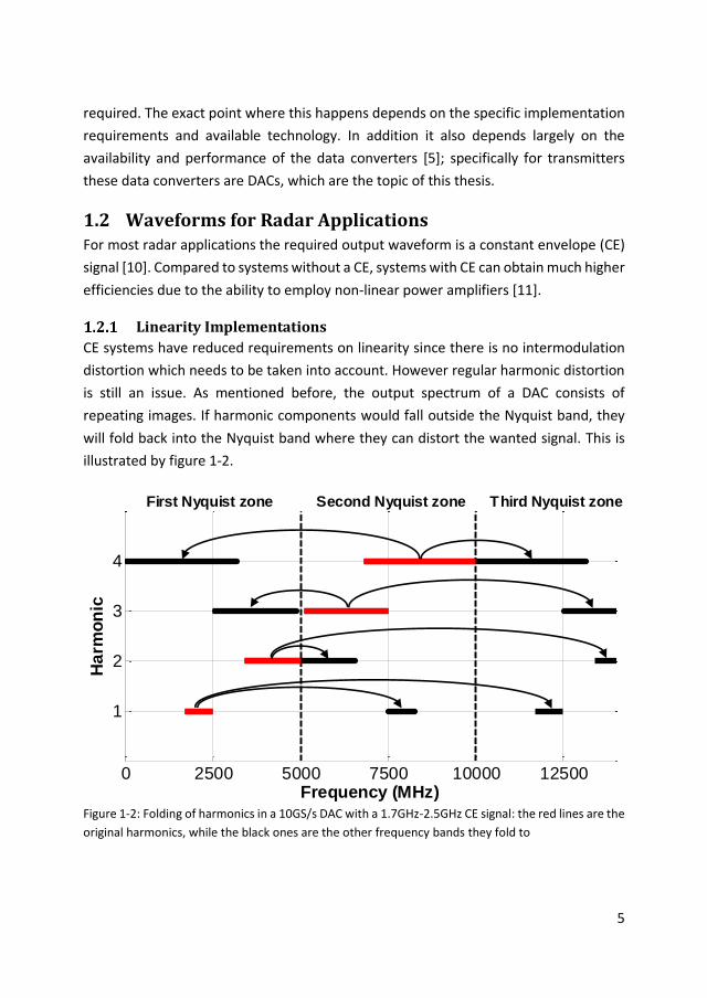
illustrated by figure 1-2.
Figure 1-2: Folding of harmonics in a 10GS/s DAC with a 1.7GHz-2.5GHz CE signal: the red lines are the
original harmonics, while the black ones are the other frequency bands they fold to
0 2500 5000 7500 10000 12500
1
2
3
4
First Nyquist zone Second Nyquist zone Third Nyquist zone
Ha
rmo
nic
Frequency (MHz)

6
So while the harmonics will always appear inside the Nyquist band, using proper
frequency allocation it can be ensured that the harmonics do not fold into the signal
bandwidth.
An example of frequency allocation that can reduce linearity demands is shown in
figure 1-3. It represents a 10GS/s DAC with a 200MHz output bandwidth located
between 3.5 and 3.7GHz. The figure shows the locations of the different harmonics of
the DAC; the first harmonic is the fundamental output. The bandwidth taken by each
harmonic is 200MHz times n, where n is the order of the harmonic. This means that
evading higher order harmonics becomes progressively harder. However since the
magnitude of higher order harmonics will normally be smaller than lower order
harmonics this is usually acceptable. In the shown example the first harmonic inside the
signal band is the 10th harmonic, the first odd harmonic is the 13th harmonic. This will
give an SFDR inside the signal band which is a lot better than the complete Nyquist
performance. The number of harmonics that can be kept outside the signal band
depends on the bandwidth and frequency planning. In general a higher Nyquist
bandwidth allows for more space, which allows for better frequency planning and less
harmonics that end up in the signal band.
Figure 1-3: Harmonics locations of a 10GS/s DAC with 200MHz signal bandwidth and n*200MHz
bandwidth for each harmonic
0 1000 2000 3000 4000 5000
123456789
10111213
200MHz BW
Ha
rmo
nic
Frequency (MHz)
7
The DAC will also generate relative strong image frequencies outside the Nyquist band.
A band pass filter would be required to pass the wanted signal band while blocking the
unwanted harmonics and image frequencies outside the signal band.
Phase Noise
An important requirement of generated signals for the use in radar systems is that the
phase noise of the generated signal must be low. A widely used signal in radar systems
is a chirp which is a sine wave with increasing frequency. Chirps can be generated by
DACs or by PLLs [12]. Comparing chirp generating DACs and PLLs in terms of e.g. phase
noise is not directly possible, since a PLL has a low frequency input which it multiplies
to get the high output frequency, while a DAC has a high frequency input that it divides
down to get a lower output frequency. So a DAC would require also a PLL to first
generate a (stable) high frequency clock input, which it can divide down to generate
the required chirp. An advantage for a DAC-based chirp generator is that a single high
performance stable clock can be shared by many DACs.
Although (phase) noise performance was not a design consideration for the DACs
presented in the thesis, a basic comparison can still be made with PLL systems. The PLL
design from [12] is optimized for generating fast chirps, something a high-speed DAC
would also be able to generate. The design in [12] achieved a phase noise of -92dBc/Hz
at a 1MHz offset with a carrier frequency of 4GHz.
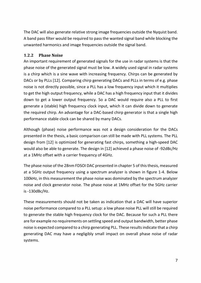
The phase noise of the 28nm FDSOI DAC presented in chapter 5 of this thesis, measured
at a 5GHz output frequency using a spectrum analyzer is shown in figure 1-4. Below
100kHz, in this measurement the phase noise was dominated by the spectrum analyzer
noise and clock generator noise. The phase noise at 1MHz offset for the 5GHz carrier
is -130dBc/Hz.
These measurements should not be taken as indication that a DAC will have superior
noise performance compared to a PLL setup: a low phase noise PLL will still be required
to generate the stable high frequency clock for the DAC. Because for such a PLL there
are for example no requirements on settling speed and output bandwidth, better phase
noise is expected compared to a chirp generating PLL. These results indicate that a chirp
generating DAC may have a negligibly small impact on overall phase noise of radar
systems.

8
Figure 1-4: Measured phase noise at 5GHz carrier using 28nm 11GS/s DAC
Quantization noise
Quantization noise is the noise-like error generated due the finite number of bits. This
error is spread out across the entire Nyquist band. If only part of the Nyquist band is
used for the signal, the system is oversampling. In this situation the effective
quantization noise in the signal band is reduced: every factor of four larger Nyquist
bandwidth compared to the signal bandwidth results in effectively an extra bit for noise
performance [13]. When the required number of bits is due to demands on the
quantization noise of the converter, this means that with increasing oversampling ratio
a lower number of bits is required while still meeting the required (in band) noise
density.
Besides the noise performance, also the obtainable linearity is dependent on the
number of bits [14]. Additionally adding/removing an LSB generally has little influence
on total power consumption; the small extra current and switches require little (drive)
power.
-80
-90
-100
-110
-120
-130
-140
-150
-160
-170

9
1.3 DAC Performance Figures The goal of a DAC is to reproduce the digital input signal in the analog domain.
Therefore main performance indicating figures represent a measure on the accuracy of
the reproduction of the digital signal in the analog domain. Noise on the output signal
is one aspect, this can both be ‘normal’ noise on the output signal, including
quantization noise, and phase noise in the clock circuitry. Generally the overall
performance of a high-speed DAC will not be limited by noise. The typically used
architectures produce inherently little noise while due to demands on the delivered
output power the signal levels are high, resulting in a large signal-to-noise ratio.
Linearity
The DACs presented in this thesis are mainly optimized for high-speed and linearity.
Ideally the conversion from the digital domain to the analog domain is perfectly linear;
in practice this is never the case. Nonlinearities give rise to harmonic distortion tones
in the output, as described in section 1.2.1, even if these would appear to fall outside
the Nyquist bandwidth, they fold back inside the Nyquist zone. Additionally there might
be non-harmonic spurs in the output signal of the DAC. These non-harmonic spurs
either have no relation to the fundamental frequency, such as a spur due to another
clock in the system, or which have a different relation to the fundamental than a regular
harmonic has.
The linearity and spur performance can be quantified in two ways. The first way is
intermodulation performance. In this, two digital sine waves with close together
frequencies that have a fixed frequency spacing are generated, each with half the full
scale amplitude. These sine waves are digitally added and used as input for the DAC. In
the analog output spectrum of the DAC, besides the two input tones this creates also
IM3 tones, as shown in figure 1-5. The difference between the power in the wanted
tones and the generally dominant third order intermodulation products can be
calculated for different signal frequencies, resulting in an IM3 versus frequency graph.
A second performance indicator is the spurious-free-dynamic-range (SFDR). For this a
single, full scale, digital sine wave is generated and used as input for the DAC. In the
resulting analog output spectrum of the DAC the difference between the power in this
tone and the largest spurious tone is taken. This takes not only harmonics, but also
other possible spurs into account and gives an SFDR value for each signal frequency. It
is important to explicitly take the bandwidth where the spurious tones must reside into

10
account. An often used approach, which is also used in the rest of this thesis, is to take
every spur in the entire used Nyquist zone into account. However sometimes only part
of the Nyquist bandwidth is taken into account, which disregards any signal outside that
part of the Nyquist band and which therefore results in a more optimistic SFDR [15].
Figure 1-5: a) Spectrum with IM3 definition, b) spectrum with SFDR definition
1.3.1.1 DNL and INL
A widely used metric to describe DC linearity in DACs is the Differential-Non-Linearity
(DNL) and Integral-Non-Linearity. The DNL is the difference between the size of an
actual output step and its ideal value. The INL is the difference between the sum of all
previous output steps and the corresponding ideal value. Figure 1-6 illustrates these
definitions. It should be noted that while for clarity a staircase is drawn, in reality non-
integer digital input codes do not exist, so also no corresponding analog output value
exists. Generally the INL and DNL are described using a single number by taking the
maximum value of all steps as the reported DNL/INL values.
In this thesis the DNL and INL are not a goal but a method: the goal is to achieve a
sufficiently high SFDR and to do this the DNL and INL inherently need to be sufficiently
low.
Frequency →
Po
we
r →
Input: f1 f2
Frequency →
Po
we
r → SF
DR
a) b)
2f1- f2→ ←2f2- f1
Input→
HD2HD3
Spur Spur
IM3

11
Figure 1-6: DNL/INL definition
Sample Rate and Bandwidth
Besides good accuracy the second requirement of a high-speed DAC is that it is fast.
The speed of a DAC is specified in terms of both analog signal bandwidth and the sample
rate of the converter. The signal bandwidth of a regular, non-undersampling, converter
can at most be equal to the Nyquist bandwidth: half the sampling frequency. At a fixed
signal bandwidth, a higher sample frequency can be beneficial: image frequencies are
moved further away from the signal band, thereby reducing demands on filtering, see
also the introduction of this chapter.
Power Consumption and Area
A certain amount of power and area will be used to obtain the given sample speed and
accuracy. Low power consumption is essential for many applications. For mobile
applications it increases battery life and in general it reduces requirements on cooling.
The cost of an IC is directly dependent on the area used. A small chip area implies that
it is cheap and it also makes integration with other circuitry easier.
An
alo
g o
utp
ut
→
Digital input code →
INL
LSB size
DNL
Ideal output

12
Figures-of-Merit
To aid comparisons between different architectures a FoM (Figure-of-Merit) can help.
A FoM aims at simplifying the relations between different parameters and combine it
into a single number which can be compared with competing designs. For example
generally if you double the power consumption, the SNR (Signal-to-Noise Ratio) will
improve with 3dB in a typical analog circuit. This implies that a design with 3dB better
SNR, but four times the power as another design, is a worse design, assuming
everything else is equal. In practice everything else will not be equal, and a design with
worse FoM can still have superior performance in other areas. Still a good FoM is a
useful tool.
The usefulness of FOMs is illustrated by the related field of ADCs (Analog-to-Digital
Converters), where designs are compared based on their FoM. Generally for low
resolution ADCs (<10 bit) Walden’s FoM [16](1-1) is used, while higher resolution ADCs,
which are more often thermal noise limited, use a modification of Schreier’s FoM [17]
which also takes distortion into account [18](1-2). The main difference between the
used FoMs is if energy scales with a factor of two per extra effective bit, or with a factor
of four.
FOMWalden =𝑃
2𝐸𝑁𝑂𝐵 ∗ 𝑓𝑠 (1-1)
FOMSchreier−modified = 𝑆𝑁𝐷𝑅 + 10 log10 (𝐵𝑊
𝑃) (1-2)
Here P is the consumed power, ENOB the effective number of bits, fs the sampling rate,
SNDR the Signal-to-Noise-and-Distortion Ratio and BW the Nyquist bandwidth.
In contrast to the ADC field, in DACs the usage of FoMs is much more limited, and they
are not used in this thesis. ADCs are often largely noise limited in performance, however
high-speed DACs are mainly limited by distortion. While a clear tradeoff between power
and noise performance can generally be found, there is no clear tradeoff between
power and linearity. This is further complicated when clock speed/Nyquist bandwidth
is added to the equation. In a noise limited system where the majority of the power
consumption is dynamic (scaling with clock speed), halving the clock speed will also cut
power consumption with a factor two while keeping the other metrics largely equal.
However even if we assume power consumption of a DAC is mainly dynamic, which

13
often is not the case, halving their clock frequency will also have a large effect on their
linearity.
Despite this various FoMs have been suggested for DACs, although they have never
received widespread acceptation. Below some of proposed FoMs are briefly discussed.
FoM #1
A FoM which is for example used in [19], and which is seen in publications on very high-
speed DACs (10-40GS/s) is given by
𝐹𝑜𝑀 =𝑃
2𝑁𝑓𝑠𝑎𝑚𝑝𝑙𝑒. (1-3)
In this equation, 𝑃 is the power consumption of the circuit, 𝑁 the number of bits, and
𝑓𝑠𝑎𝑚𝑝𝑙𝑒the sampling frequency of the system. While some of the designs in this thesis
would do very well when this FoM is taken into account, it is not a very useful one. Since
the accuracy of the conversion is ignored, the best FoM would be achieved by disabling
the IC. Clearly accuracy needs to be taken into account to have a useful FoM.
FoM #2
Another known FoM was introduced in [20] as
𝐹𝑜𝑀 =𝑉𝑠𝑤𝑖𝑛𝑔𝑓𝑠𝑖𝑔
𝑃10
𝑆𝐹𝐷𝑅[𝑑𝐵]20 (1-4)
in which 𝑉𝑠𝑤𝑖𝑛𝑔is the swing at the output of the DAC and 𝑓𝑠𝑖𝑔 is the frequency of the
used test tone. This FoM does take the linearity into account in the form of the SFDR.
However the output swing of a current DAC can easily be increased by for example
using a (more) high-ohmic load resistance, at which point it depends on the dominant
distortion mechanism whether the SFDR would decrease. As alternative the load
resistance could be increased while the output current is decreased, which should
lower power consumption while not changing any of the other parameters. In addition
it assumes that with doubling the power the obtainable signal frequency at a given
swing and SFDR can also be doubled, which is questionable.

14
FoM #3
In [21] another FoM is given by:
𝐹𝑜𝑀 =2𝐸𝑁𝑂𝐵𝐷𝐶2𝐸𝑁𝑂𝐵𝑁𝑦𝑞𝑓𝑠𝑎𝑚𝑝𝑙𝑒
𝑃𝑡𝑜𝑡𝑎𝑙 − 𝑃𝑙𝑜𝑎𝑑 (1-5)
In this equation 𝐸𝑁𝑂𝐵𝐷𝐶 is the effective number of bits at DC, and 𝐸𝑁𝑂𝐵𝑁𝑦𝑞 is the
effective number of bits at Nyquist. Furthermore it subtracts the power delivered to
the output from the power consumption, which results in a more fair estimation of the
actually dissipated power. But the advantage of including the DC performance is not
clear: generally the worst-case performance is what should be taken into account for a
system, and a typical high-speed DAC is never intended to have an exceptional DC
performance. Placing an audio DAC in parallel to the actual DAC, which would then be
used for only low frequency signals would result in a very good FoM, while it obviously
is not a useful setup. In addition it also assumes that doubling the sample rate at equal
ENOB would require only a doubling of power consumption.
FoM #4
Two related FoMs are used in [22]:
𝐹𝑜𝑀 =2𝑁𝐵𝑊70𝑑𝐵
𝑃 (1-6)
𝐹𝑜𝑀 =2𝑁𝐵𝑊70𝑑𝐵𝑃 ∗ 𝐴
(1-7)
The 𝐵𝑊70𝑑𝐵is the bandwidth where the SFDR is more than 70dB, and 𝐴 is the core area.
Taking the area into account is an improvement, although it is not clear why this specific
relation would hold across different designs. Using the 70dB bandwidth (or another
number) is advantageous for a design with a linearity slightly over 70dB across a large
frequency range, while it would severely penalize designs which are slightly below
70dB. Such a metric could be appropriate if there was a clear relationship between
signal frequency and SFDR. However since this is not the case for many designs it is not
a good performance parameter.
Conclusion on DAC FOMs
Despite all the problems mentioned on existing FOMs, there were many attempts to
introduce a suitable FoM for (high-speed) DACs. A FoM will never take every relevant
parameter into account and it will also never be a perfectly fair comparison, doing that

15
with a single number is not a realistic expectation. So when evaluating proposed FoMs
it should be taken into account that it will not and is not intended to be a perfect
representation of the overall performance of a design. However the FoMs discussed
here either lack important performance figures, or they do not accurately model
relationships between the performance figures. Also for all the FoMs discussed here,
neither empirical nor fundamental evidence has been presented to support the
relationships between different parameters that they assume exist has been shown.
For these reasons in this thesis no FoMs are used to compare performance. Instead the
raw performance figures are listed and compared directly.
1.4 DAC architectures Many different architectures that are capable of implementing digital-to-analog
conversions are known. Since the focus in this thesis is on DACs for RF applications, only
DAC architectures that are capable of high-speed operation are discussed. [23, 24]
Different oversampling and noise-shaping techniques are not discussed here; while
these architectures are very capable of generating good performance at lower signal
bandwidths, due to their oversampling nature they are not suitable for the signal
frequencies required in this research.
Charge-Redistribution DAC
The charge-redistribution DAC is found in two flavors: it can be implemented in a serial
and in a parallel fashion. The serial implementation requires a clock cycle per bit, while
the parallel version can do an entire conversion in a single cycle.
Figure 1-7 shows an example of a parallel charge-redistribution DAC. It consists of an
array of binary scaled capacitors. Initially these are all charged to a common voltage,
after which the bottom plates of the capacitors can be switched to a reference voltage.
Depending on the size of the switched capacitor, this causes a redistribution of the
charge, and generates an output voltage which depends on the digital code [25].

16
C2C4C8C
Output
Vref
Figure 1-7: Parallel charge-redistribution DAC
The serial charge-redistribution DAC consists of only two equal sized capacitors, and is
an LSB-first multi-step architecture. The first half of each cycle the two capacitors are
disconnected, and one of them is either charged to a reference voltage, or discharged
to ground. The second half the two capacitors are connected, allowing the charge to be
redistributed with the charge on the other capacitor which is from the previous steps
[26]. While it requires fewer capacitors than the parallel version requires, the matching
demands are similar, so the capacitor area required is also similar. The serial
implementation is more flexible, but due to its much lower speed generally the parallel
version is preferred.
C C
OutputVref
Figure 1-8: Serial charge-redistribution DAC
17
These DACs are often used in SAR (Successive-Approximation-Register) ADCs, where
they are directly connected to a comparator. For most other applications a buffer would
be required after the capacitors.
R-2R Ladder DAC
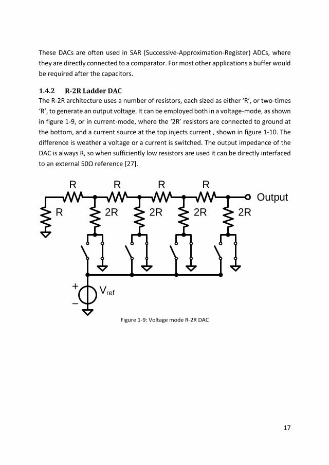
The R-2R architecture uses a number of resistors, each sized as either ‘R’, or two-times
‘R’, to generate an output voltage. It can be employed both in a voltage-mode, as shown
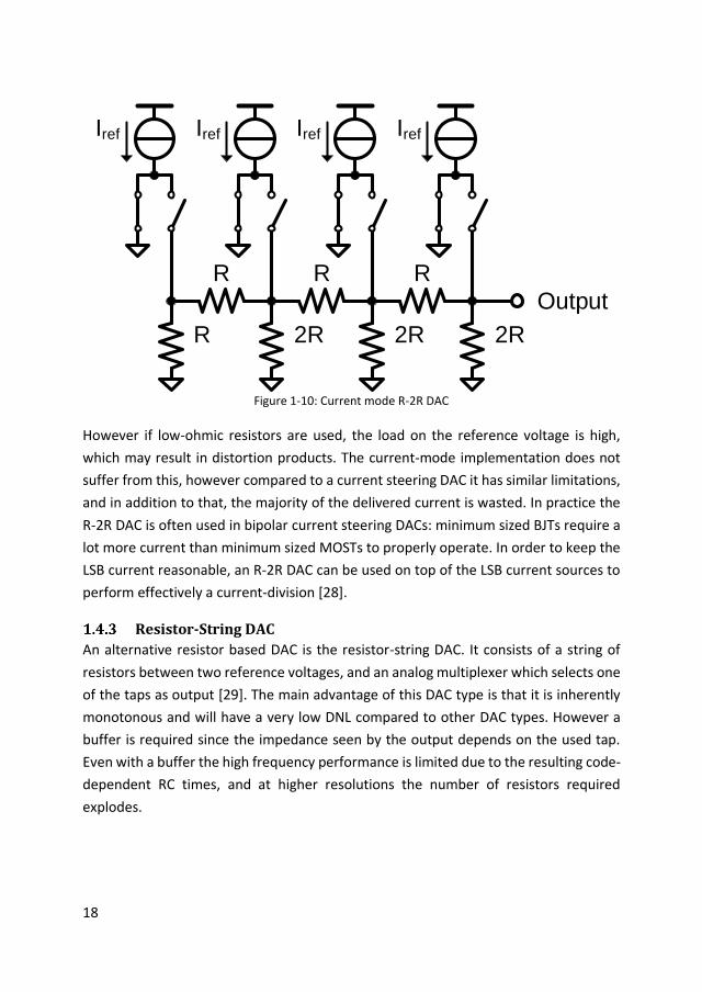
in figure 1-9, or in current-mode, where the ‘2R’ resistors are connected to ground at
the bottom, and a current source at the top injects current , shown in figure 1-10. The
difference is weather a voltage or a current is switched. The output impedance of the
DAC is always R, so when sufficiently low resistors are used it can be directly interfaced
to an external 50Ω reference [27].
R
R
2R
Vref
R
2R
R
2R
R
2R
Output
Figure 1-9: Voltage mode R-2R DAC
18
Figure 1-10: Current mode R-2R DAC
However if low-ohmic resistors are used, the load on the reference voltage is high,
which may result in distortion products. The current-mode implementation does not
suffer from this, however compared to a current steering DAC it has similar limitations,
and in addition to that, the majority of the delivered current is wasted. In practice the
R-2R DAC is often used in bipolar current steering DACs: minimum sized BJTs require a
lot more current than minimum sized MOSTs to properly operate. In order to keep the
LSB current reasonable, an R-2R DAC can be used on top of the LSB current sources to
perform effectively a current-division [28].
Resistor-String DAC
An alternative resistor based DAC is the resistor-string DAC. It consists of a string of
resistors between two reference voltages, and an analog multiplexer which selects one
of the taps as output [29]. The main advantage of this DAC type is that it is inherently
monotonous and will have a very low DNL compared to other DAC types. However a
buffer is required since the impedance seen by the output depends on the used tap.
Even with a buffer the high frequency performance is limited due to the resulting code-
dependent RC times, and at higher resolutions the number of resistors required
explodes.
R
R
2R
R
2R
R
2R
Output
Iref Iref Iref Iref
19
R
R
R
R
R
Vref
Output
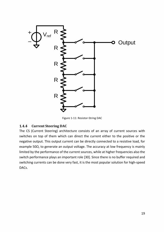
Figure 1-11: Resistor-String DAC
Current Steering DAC
The CS (Current Steering) architecture consists of an array of current sources with
switches on top of them which can direct the current either to the positive or the
negative output. This output current can be directly connected to a resistive load, for
example 50Ω, to generate an output voltage. The accuracy at low frequency is mainly
limited by the performance of the current sources, while at higher frequencies also the
switch performance plays an important role [30]. Since there is no buffer required and
switching currents can be done very fast, it is the most popular solution for high-speed
DACs.
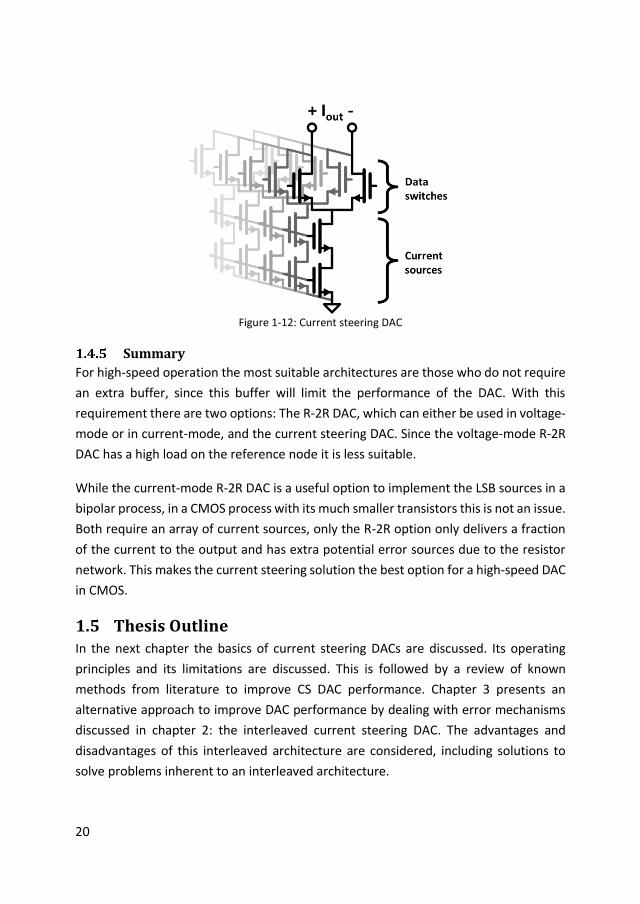
20
Figure 1-12: Current steering DAC
Summary
For high-speed operation the most suitable architectures are those who do not require
an extra buffer, since this buffer will limit the performance of the DAC. With this
requirement there are two options: The R-2R DAC, which can either be used in voltage-
mode or in current-mode, and the current steering DAC. Since the voltage-mode R-2R
DAC has a high load on the reference node it is less suitable.
While the current-mode R-2R DAC is a useful option to implement the LSB sources in a
bipolar process, in a CMOS process with its much smaller transistors this is not an issue.
Both require an array of current sources, only the R-2R option only delivers a fraction
of the current to the output and has extra potential error sources due to the resistor
network. This makes the current steering solution the best option for a high-speed DAC
in CMOS.
1.5 Thesis Outline In the next chapter the basics of current steering DACs are discussed. Its operating
principles and its limitations are discussed. This is followed by a review of known
methods from literature to improve CS DAC performance. Chapter 3 presents an
alternative approach to improve DAC performance by dealing with error mechanisms
discussed in chapter 2: the interleaved current steering DAC. The advantages and
disadvantages of this interleaved architecture are considered, including solutions to
solve problems inherent to an interleaved architecture.

21
In chapter 4 a practical implementation of the interleaved DAC architecture proposed
in chapter 3 is presented. Circuit solutions to deal with limitations of the used
architecture are shown, followed by measurement results obtained with the designed
chip. The last part of this chapter summarizes the suitability of the interleaved DAC
architecture for high-speed signal generation.
While the presented interleaved DAC architecture suppresses many of the spurs
generated by regular DACs, it is not able to nullify all of them. At high-speeds especially
data-dependent load on the bias and power supply lines is still problematic. Chapter 5
gives an in-depth analysis of these issues and proposes a solution to reduce their
impact. It is followed by an implementation of the solution in a designed DAC and the
performance obtained by that DAC.
Finally chapter 6 summarizes the results presented in this thesis and presents the
conclusions, followed by recommendations to further improve the performance of
high-speed DACs.


23
The Current Steering DAC
The subject of this thesis is the design of high-speed DACs. As argued in chapter 1, the
best suited conventional DACs for this application are the current steering (CS) digital-
to-analog converters (DACs). These are commonly used to generate high-frequency
signals, and they consist of an array of current sources and current-switches as depicted
in figure 2-1. Depending on the digital code, current is switched either to the positive
or the negative output.
Since the current switches only are required to redirect the fixed current generated by
their corresponding current source, this can be done both fast and accurately. The
output current can often be fed directly into a 50Ω load, removing the need for a buffer
that would both be power hungry and would introduce additional non-linearities.
Distortion components in the DAC’s output current are due to both static and dynamic
error mechanisms. Static errors include those due to mismatch between current
sources and those due to the finite output resistance of the current sources. Dynamic
errors are due to e.g. timing errors at the switching moment, glitches of the switches
and output capacitance of the current sources. High-speed DACs are typically limited in
their linearity by dynamic errors; static errors can generally be sufficiently suppressed
to not limit the high frequency performance.

24
Figure 2-1: Current steering DAC
2.1 Static error mechanisms Static errors in CS DACs are mainly due to non-perfect current sources. An ideal current
source has exactly the correct current output and hence has an infinite output
impedance. However both of these properties are not satisfied for a real current source
realized using mosfets. The following two section discuss in some detail these two non-
idealities. For the output impedance only the real part of the output impedance, the
output resistance, is taken into account because the imaginary part results in a dynamic
error.
The two mechanisms described above are usually dominant. Other errors sources that
can be made sufficiently small include layout issues. For example in the layout
especially the impedance of the ground connection of the current sources should be
matched in order not to give rise to inequalities between sources due to IR drop.
Output resistance
The finite output resistance of a current source results in variations in the output
current that are dependent on the output voltage. This results in mainly second order
distortion, which is suppressed by the differential nature of the architecture. However
there are also higher order distortion components present due to finite, constant,
output resistance of the current sources which are not suppressed by the differential
architecture. The INL of a differential DAC with sources that have finite output
resistance is given by [31]:

25
𝐼𝑁𝐿 =−𝑔𝐿𝑔𝑜
2𝑘(2𝑘 − 𝑁)(𝑁 − 𝑘)
2(𝑔𝐿2 + 𝑔𝐿𝑔𝑜𝑁 + 𝑔𝑜
2𝑘𝑁 − 𝑔𝑜2𝑘)(𝑔𝐿 +𝑁𝑔𝑜)
(2-1)
Here 𝑔𝐿 is the load conductance, 𝑔𝑜 is the output conductance of a unit cell, 𝑘 is the
input code and 𝑁 equals 2𝑏𝑖𝑡𝑠, this is illustrated by figure 2-2. Figure 2-3 shows the
calculated INL for a 10-bit DAC with 300kΩ output resistance for a unit current source,
into a 50Ω load.
1/go
1/gL 1/gL
xN
+ Vout -
k k
Figure 2-2: Definitions used to calculate the INL as function of current source output resistance
Figure 2-3: INL versus code of 10-bit DAC with 50Ω load and constant 300kΩ unit output resistance
0 200 400 600 800 1000
-1
-0.5
0
0.5
1
INL
(L
SB
)
Code

26
Output current variations
Even when subjected to equal electrical conditions the current sources can have
different output current due to a variety of causes. Mismatch is always a cause for
variations between transistors. This is generally described by Pelgrom’s Law [32](2-2),
from which it follows that the variance of the output current of a current source is
inversely proportional to the area of the current source transistor. So if the standard
deviation needs to be decreased by a factor of two, the area needs to be increased by
a factor four.
𝜎 =K
√W ∗ L (2-2)
In this equation σ is the standard deviation of the investigated parameter, K is the
standard deviation for a 1μm2 device, and W and L are the dimensions in μm.
In addition to this mismatch, also gradients due to any non-uniformities in the chip
fabrication play a role. Generally common-centroid layouts are used to limit their
influence, although the exact influence of this gradient when a small current source
matrix is used with today’s large wavers is unknown.
Finally proximity effects also play an important role. Each current source should ‘see’
the same environment: if a current source at the edge of the matrix is close to another
well, this will affect its characteristics. For this reason the current sources need to be
surrounded by dummy devices, which have as goal to create an equal environment for
all the actually used current sources.
2.2 Dynamic mechanisms Many significant dynamic error mechanisms are present in CS DACs. One of the major
dynamic error mechanisms is non-exact timing in the data switches. Timing errors can
be variable, due to e.g. data-dependent clock loading, or they can be static, due to e.g.
random mismatch or layout issues. For high-speed DACs with sample frequencies above
1GHz and moderate to high linearity requirements (higher than 50dB), timing errors are
required to be in the sub-picosecond range, which is tough to achieve.
Other timing related errors are due to e.g. break-before-make behavior of switches that
have periodically both switches in their off-state during switching, leaving the current
source disabled and forcing some kind of recovery behavior after switching. Further

27
significant timing related error mechanisms are due to differences in rise and fall times
of the switches and effects such as clock feed through that all create spurs in the DAC’s
output signal.
In conventional CS DACs, the data switches switch only if the new code is different from
the previous code: the amount of switching is hence code-dependent. Code-dependent
switching introduces code-dependent load on the power supply, and induces
disturbances to e.g. the bias lines. Both of these effects yield unwanted modulation of
the output signal. Current-mode logic may be used to reduce the impact of this, but for
complete suppression the switching fundamentally needs to be data-independent,
which can for example be achieved with RZ-switching or quad-switching [33].
A last significant source of dynamic errors is the output capacitance of the current
sources. While this capacitance usually is very linear, these capacitances are data-
dependently switched to either the positive or the negative output. Together with the
load impedance they form a code-dependent RC filter, which results in spurs.
All these dynamic error mechanisms start at the switching time instance and last for a
fraction of the sample period. The timing and switching related errors can have a large
impact despite occurring only for a picosecond or even less.
2.3 Recent Literature In the recent years new techniques have been developed to deal with dynamic errors
that limit high-speed performance in CMOS DACs. Recently published DACs with high
sample rates and >6-bit resolution are discussed in sections 2.3.1 through 2.3.5.
Extra Cascodes with Bleeding Current Sources
In [34, 35] a solution is proposed to eliminate the error due to the code-dependent
capacitance seen at the output terminals of the DAC. This solution is shown in figure
2-4.
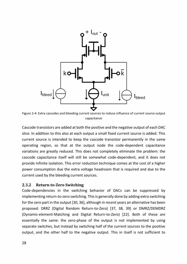
28
Iunit
+ Iout -
Ibleed Ibleed
k k
Figure 2-4: Extra cascodes and bleeding current sources to reduce influence of current source output
capacitance
Cascode transistors are added at both the positive and the negative output of each DAC
slice. In addition to this also at each output a small fixed current source is added. This
current source is intended to keep the cascode transistor permanently in the same
operating region, so that at the output node the code-dependent capacitance
variations are greatly reduced. This does not completely eliminate the problem: the
cascode capacitance itself will still be somewhat code-dependent, and it does not
provide infinite isolation. This error reduction technique comes at the cost of a higher
power consumption due the extra voltage headroom that is required and due to the
current used by the bleeding current sources.
Return-to-Zero Switching
Code-dependencies in the switching behavior of DACs can be suppressed by
implementing return-to-zero switching. This is generally done by adding extra switching
for the zero part in the output [30, 36], although in recent years an alternative has been
proposed: DRRZ (Digital Random Return-to-Zero) [37, 38, 39] or DMRZ/DEMDRZ
(Dynamic-element-Matching and Digital Return-to-Zero) [22]. Both of these are
essentially the same: the zero-phase of the output is not implemented by using
separate switches, but instead by switching half of the current sources to the positive
output, and the other half to the negative output. This in itself is not sufficient to

29
suppress spurs. However there are many settings which result in equal positive and
negative output currents which can implement the zero-phases, the number of possible
combinations is given by ( 2𝑏𝑖𝑡𝑠
2𝑏𝑖𝑡𝑠−1) . For a 6-bit section this equals 1.8𝐸18
combinations. By digitally randomizing the combination which is used at every zero-
phase, spurs are effectively transformed into noise and the advantages of RZ switching
schemes are obtained without extra switches being required.
However at the same time return-to-zero switching also has significant downsides [40].
With the same output voltage swing they deliver less output power in the primary
Nyquist zone, while the power of the image frequencies is larger, requiring steeper anti-
alias filters. Additionally they are more sensitive to jitter, and the internal switching
frequencies need to be higher compared to a NRZ DAC, limiting its usefulness for very
high-speed DACs.
Quad-Switching
Quad-switching is an older technique, first shown in [41], and more recently in [15].
Instead of one set of switches per current source to redirect the current to the positive
or to the negative output, it uses four switches as shown in figure 2-5, with inputs
𝑘1, 𝑘2, 𝑘3̅̅ ̅ and 𝑘4̅̅ ̅. Of these inputs only one is high at a time.
k2k1 k3 k4
I- I+
Figure 2-5: Quad-Switching Current Cell

30
In a regular architecture the switch activity depends on whether the code changes or
not. In a quad-switching architecture each clock cycle one switch turns off, and one
switch turns on, removing the code-dependency from the switching activity. This is
illustrated by figure 2-6 and further elaborated on in chapter 5. The downside of this is
that the average switching activity increases, and it costs a bit more area. Another
potential problem is that the number of switches increase, and so does the potential
for timing related problems. Part of these can be moved out of the signal band by
running the quad-switching at twice the data rate [42], however doubling the switch
frequency without actually increasing the sample rate is also not ideal for high-speed
DACs. [43] presents this technique as dual return-to-zero, although normally dual
return-to-zero consists of two RZ DACs in parallel, which is clearly not the case here.
I- I+ I- I+ I- I+‘0’ ‘0’ ‘1’
Figure 2-6: Quad-switching states for three consecutive clock cycles with outputs ‘0’-‘0’-‘1’. The grey
transistors are turned off, while the black ones are enabled
Interleaved DACs
The interleaved CS DAC architecture that is the main topic of this thesis, has in recent
years also been presented by other groups.
The work presented in [44] also uses an interleaved architecture to suppress switching
induced spurs. They included digital pre-distortion to further lower some of the spurs,
and made different design decisions compared to the work presented here; the system
level design is similar, but the implementation of the sub-blocks are different. This
results in very good IM3 performance, below -74dBc up to 1GHz, at the cost of a high
power consumption (2.3W) and core area (5.2mm2). This is one-two orders more than
what is used by our designs in chapter 4 and 5.
Another type of interleaved DAC, which is discussed in [45, 46, 47], also consists of
several sub-DACs in parallel, however in contrast to the work presented in this thesis

31
and the work of [44], no multiplexer is used to combine them and instead the output
currents of all sub-DACs are directly summed. While this does still double the sample
rate, it does not provide the other benefits that an interleaved architecture can give.
When the connected sub-DACs are RZ DACs, this is also presented as dual return-to-
zero [40].
In [48, 49, 50, 51] also interleaved architectures are shown, however these have only
reported idealized simulation results, which cannot be compared to measured results.
Other publications
Many other publications are available that try to reduce distortion components of high-
speed DACs. For example reduction of differences between different binary scaled
sources was achieved by adding replica circuits in [52]. In [53, 54] high operating speed
with low power consumption is achieved using a binary structure which consists of
parallel unit cells, instead of combining them as one large cell, concluding that at least
for a limited number of bits good performance can be achieved while using a binary
decoding. At similar speeds [55] achieves improved performance by using a custom
CML latch to improve performance, and where the DAC is optimized for low area, which
also limits the size of layout parasitics. Additionally it also employs replicas for reducing
differences between different bits, however these are operated at reduced current to
lower power consumption.
While full sigma-delta implementations are not fast enough yet for the frequencies
considered here, the hybrid implementation shown in [56], which uses both a Nyquist
rate part and a sigma-delta part, achieves a signal bandwidth of 500MHz with good
linearity, although that is including digital predistortion.
By randomizing which unit cells are used at any time to create a binary scaled source,
[57] can decrease the mismatch induced distortion components. In [58] an active
calibration is used to reorder the switching sequence such that the INL is optimized: a
smaller-than-nominal current cell will be followed by a larger-than-nominal one. This
sorting algorithm is further improved on in [59], which uses a 3D calibration technique.
This method is not only capable of reducing distortion at low, but also at high
frequencies by pairing current cells with opposite (compensating) behavior. This seems
to work well for IM3 performance, boosting it by 10dB over Nyquist, but appears to
have little influence on the SFDR.

32
By adding extra switches that can invert the signal, [60] is effectively integrating a
current-mode mixer. This mixer has a fixed frequency equal to the sampling rate and a
variable duty cycle. This adds the option to invert the output current during a part of
each sample period, allowing the DAC to make effective use of multiple Nyquist zones.
The main advantage compared to simply sampling faster should be found in the relative
low power consumption.

33
The Interleaved Structure
This chapter is based on [61], starting from section I-B up to section II, and section IV in
[61]. Compared to [61] the differences between different operating region for the
multiplexer transistors is described more in-depth.
The dynamic errors in CS DACs are present at the switching time and during a short
period after the switching time instances. During the remainder of a sampling period,
the effect of these dynamic errors can be sufficiently small. Consequently, the linearity
of a CS DAC can be improved if we make sure the DAC is not connected to the output
during the time that the dynamic errors are significant; this is for example done in [30,
36] in the form of an RZ output signal. However as mentioned in section 2.2, RZ results
in much larger transients and increases demands on analog post-filtering while at the
same time the delivered output power is decreased. This can be improved by using two
sub-DACs (sDACs) that operate alternatingly by using opposite clock phases: then each
sDAC can be connected to a dummy output during the switching moment thereby
placing the timing and settling related errors on only the dummy output. Once settled,
the sDAC’s output can be routed to the actual output, and meanwhile the other sDAC
can switch to and settle to its new code. The corresponding interleaved architecture for
this is shown in figure 3-1. In this figure sDAC-A and sDAC-B are alternatingly switched
to the actual output and to a dummy output by the multiplexer. Note that while this
interleaved approach doubles the required area and power compares to the RZ variant,
it also doubles the sampling rate without requiring higher switching frequencies and
outputs a regular, non-return-to-zero, waveform.
34
Several other interleaving architectures are known from literature; a brief discussion is
given below. Placing multiple sDACs in parallel and shorting their outputs is sometimes
classified as interleaving [62]. However while this is easy to implement and while it does
double the sampling rate, it does not solve issues such as timing mismatch and code-
dependent settling speed. Since it sums the currents it does not output the converted
digital input word, but the sum of the last two, modifying the frequency response. This
last issue can be solved by implementing RZ switching in each sDAC cell [63] which
makes sure that only the current code is converted to the output, and at the same time
it adds some of the advantages of an RZ DAC. However it does not remove all of the
timing and settling issues associated with conventional RZ DACs.
In this paper, the focus is on two-times-interleaved CS DAC architectures with a central
multiplexer to combine the outputs. Higher interleaving counts can be used, but two-
times interleaving will already suppress all timing errors sufficiently by giving enough
time for settling of nodes.
Using an interleaved architecture as low-power, area-efficient solution might seem
counter-intuitive at first; placing two sDACs in parallel doubles both area and power
consumption, and additionally also an analog multiplexer is required to toggle between
the two. However since both sDACs only run at half the overall DACs speed with
significantly reduced demands on dynamic errors for each sDAC due to the interleaving
setup, each individual sDAC can actually be small and low-power, while maintaining a
good overall interleaved DAC performance.
Interleaved DACs employing an analog multiplexer have been reported before. The
work in [64] contains the first reference to this method of removing switching
transients from the output of a DAC; using an opamp with a built-in multiplexer to
switch between two sDACs. In [49] a method to limit the impact of gain mismatch
between sDACs is presented and illustrated only using simulations on an idealized
circuit. The interleaved DACs in [65], discussed in chapter 4 of this thesis, and [66],
discussed in chapter 5, use triode switches without quad-switching to obtain 58dB SFDR
across Nyquist at 1.7GS/s. In [44] saturation switches are used; large bleeder currents
are added to improve their linearity. While the design in [44] achieves superior SFDR,
69dB, this is across less than a quarter Nyquist at 4.6GS/s and at a cost of more than
one order higher power consumption and two orders in area compared to the work in
this paper.
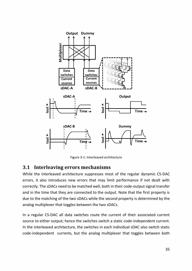
35
Figure 3-1: Interleaved architecture
3.1 Interleaving errors mechanisms While the interleaved architecture suppresses most of the regular dynamic CS-DAC
errors, it also introduces new errors that may limit performance if not dealt with
correctly. The sDACs need to be matched well, both in their code-output signal transfer
and in the time that they are connected to the output. Note that the first property is
due to the matching of the two sDACs while the second property is determined by the
analog multiplexer that toggles between the two sDACs.
In a regular CS-DAC all data switches route the current of their associated current
source to either output; hence the switches switch a static code-independent current.
In the interleaved architecture, the switches in each individual sDAC also switch static
code-independent currents, but the analog multiplexer that toggles between both

36
sDACs switches the full, code-dependent, output current. This results in additional
challenges to obtain good spectral performance compared to conventional CS DACs.
The following sections discuss the most important issues in interleaved DACs.
Static matching of the sDACs
To simplify the analysis of the overall DAC performance limitation due to static sDAC
mismatch, the output signal of the second sDAC is written as that of the first sDAC with
a code-dependent mismatch term: 𝑉𝑜𝑢𝑡,𝑠𝐷𝐴𝐶2(𝑐𝑜𝑑𝑒) = 𝑉𝑜𝑢𝑡,𝑠𝐷𝐴𝐶1(𝑐𝑜𝑑𝑒) + 𝜖(𝑐𝑜𝑑𝑒).
Each of the sDACs in the interleaved DAC runs at half the sampling frequency, with their
corresponding image frequencies. For perfectly matched sDACs, 𝜖(𝑐𝑜𝑑𝑒) ≡ 0 and the
image frequencies due to interleaving cancel each other. In that case, the harmonics
and images created by the interleaved DAC due to e.g. any non-linearity in
𝑉𝑜𝑢𝑡,𝑠𝐷𝐴𝐶1(𝑐𝑜𝑑𝑒) are exactly the same as that of a non-interleaved DAC having the
same 𝑉𝑜𝑢𝑡,𝐷𝐴𝐶(𝑐𝑜𝑑𝑒). Any mismatch 𝜖(𝑐𝑜𝑑𝑒) between the sDACs however limits the
cancellation of the image frequencies, while these images fall in-band for the complete
interleaved DAC when assuming full Nyquist operation.
In a conventional non-interleaved DAC, a DC offset has no effect on its performance. In
an interleaved DAC, a DC offset 𝜖(𝑐𝑜𝑑𝑒) =Δ between the two sDACs results in a
square wave shaped output signal running at half the sampling frequency, creating a
spur at half-FS and at DC. An illustration of this error mechanism is shown figure 3-2;
the output signals of both sDACs are shown in the top graph for a sinusoidal output,
where the output signal of sDAC-B equals the sum of the output signal that sDAC-A
would give for the same code and of a fixed offset. The lower graph in figure 3-2 shows
only this error component, scaled up by a factor 5 for illustration purposes. These
resulting spurs reside outside the Nyquist band.

37
Figure 3-2: Output of an interleaved DAC with an offset error between the sDACs
Similarly, a gain error has no effect on the output spectrum in a conventional DAC. In
the interleaved DAC, a gain error 𝜖(𝑐𝑜𝑑𝑒) = 𝜀𝑔𝑎𝑖𝑛 ∗ 𝑉𝑜𝑢𝑡,𝑠𝐷𝐴𝐶1(𝑐𝑜𝑑𝑒) generates an RZ
output signal proportional to the output signal, at half the sample frequency of the
overall system. Figure 3-3 shows an illustration of this error mechanism: the output
signals of both sDACs are shown in the top graph for a sinusoidal output. The output of
sDAC-B is subdivided into the response that sDAC-A would have given for the same code
and into the error contribution 𝜖(𝑐𝑜𝑑𝑒). The lower graph in figure 3-3 shows only this
error component, scaled up by a factor 5, which is proportional to a 50% duty cycle RZ-
version of the DAC’s output signal.

38
Figure 3-3: Output of an interleaved DAC with a gain error between the sDACs
Since 𝜖(𝑐𝑜𝑑𝑒) has half the sampling frequency of the complete DAC, it generates
signals at exactly the output frequency, adding to the main signal, and generating spurs
mirrored around half Nyquist:
𝑓𝑠𝑝𝑢𝑟 =𝑓𝑠𝑎𝑚𝑝𝑙𝑒
2− 𝑓𝑠𝑖𝑔𝑛𝑎𝑙 (3-1)
Ignoring the frequency roll-off due to zero-order hold behavior, the SFDR of the
resulting return-to-zero signal is given by:
𝑆𝐹𝐷𝑅 = 20 log10 (1
𝜖𝑔𝑎𝑖𝑛) + 6dB (3-2)
Where the 6dB is due to the 50% duty cycle of the RZ signal. When the zero-order hold
behavior is taken into account the fundamental has a 𝑠𝑖𝑛𝑐(𝑥) -shaped frequency
response. The image is a return-to-zero signal at half the sampling frequency, yielding
an equal sinc-shaped frequency response with 6dB attenuation. Noting that the image

39
frequency is mirrored around half Nyquist compared to the fundamental, the overall
attenuation of the image compared to the fundamental is given by:
𝐼𝑚𝑎𝑔𝑒𝑎𝑡𝑡𝑒𝑛𝑢𝑎𝑡𝑖𝑜𝑛 = 20 log10
(
𝑠𝑖𝑛𝑐 (
𝑓𝑠𝑖𝑔𝑛𝑎𝑙𝑓𝑠𝑎𝑚𝑝𝑙𝑒
)
𝑠𝑖𝑛𝑐 (
𝑓𝑠𝑎𝑚𝑝𝑙𝑒2 − 𝑓𝑠𝑖𝑔𝑛𝑎𝑙𝑓𝑠𝑎𝑚𝑝𝑙𝑒
)
)
(3-3)
At (near) DC signal frequency, the relative attenuation of the image according to (3-3)
is 4dB, while at (near) Nyquist signal frequency this relative image attenuation is -4dB.
This yields:
𝑆𝐹𝐷𝑅𝐷𝐶 = 20 log10 (1
𝜖𝑔𝑎𝑖𝑛) + 10 dB (3-4)
𝑆𝐹𝐷𝑅𝑁𝑦𝑞𝑢𝑖𝑠𝑡 = 20 log10 (1
𝜖𝑔𝑎𝑖𝑛) + 2 dB (3-5)
Higher order mismatch between the sDACs, where 𝜖(𝑐𝑜𝑑𝑒) = 𝜀𝑛 ∗ 𝑉𝑜𝑢𝑡,𝑠𝐷𝐴𝐶1𝑛 (𝑐𝑜𝑑𝑒),
gives harmonics of the fundamental in the output current and due to the RZ behavior
these are also folded around half-Nyquist. The effect of this higher order mismatch also
result in spurs in a similar way as in CS DACs; so the required matching to suppress the
spurs in interleaved DACs is also similar to the matching required for a regular CS DAC.
It does not matter if this higher order mismatch is common for the sDACs or opposite
to each other for the size of the resulting spur.
Dynamic matching of the multiplexer
Mismatch in the multiplexer and its driver result in a non-50% duty cycle for the
connection of either sDAC to the overall output, which in turn yields spurs in the DAC
output signal. With a non-50% duty cycle, one sDAC (e.g. the signal due to one code) is
still at the output, while the next one should already have been placed on the output.
Since this happens only at every second transition, an error is created which occurs at
only half the sample rate of the complete DAC. This spur is located at the same
frequency as an amplitude error (3-1).
Assuming a sinusoidal fundamental signal with unit amplitude and ignoring the sampled
nature of the DACs output signal, the size of the error 𝜖(𝑐𝑜𝑑𝑒) can easily be estimated.

40
Under these assumptions, the error due to non-50% duty cycle switching between the
two sDACs is a pulse train, at half the sample frequency. The amplitude of these pulses
is the difference between two consecutive samples, which can be approximated by the
derivative of the fundamental signal multiplied by the sample period, i.e. divided by its
sample frequency. In this approximation, the sinc roll-off is ignored which effectively
yields an overestimation of the error.
𝜖𝑎𝑚𝑝−𝑝𝑢𝑙𝑠𝑒 =2𝜋𝑓𝑠𝑖𝑔𝑛𝑎𝑙𝑓𝑠𝑎𝑚𝑝𝑙𝑒
cos(2𝜋𝑓𝑠𝑖𝑔𝑛𝑎𝑙𝑡) (3-6)
The duty cycle of the error pulse train is determined by the timing error, denoted as Δt,
divided by two sample times, since it only occurs once every two samples:
𝜖𝑑𝑢𝑡𝑦−𝑝𝑢𝑙𝑠𝑒 =1
2Δ𝑡𝑓𝑠𝑎𝑚𝑝𝑙𝑒 (3-7)
An illustration of this error mechanism and of the resulting error signal is given in figure
3-4. The output signals of both sDACs are shown in the top graph for a sinusoidal
output, for a 60% duty cycle for sDAC-A; the output of sDAC-A is subdivided into the
response for 50% duty cycles and into an error contribution 𝜖(𝑐𝑜𝑑𝑒). The lower graph
in figure 3-3 shows only this error component, scaled up by a factor 3.
If the sDACs’ duty cycle is almost 50%, the error pulse train has a small duty cycle
𝜖𝑑𝑢𝑡𝑦−𝑝𝑢𝑙𝑠𝑒, and the roll-off of its output spectrum is negligible for the first Nyquist
zone. The magnitude of the spurs in the signal band is simply the product of the error
amplitude in (3-6) and the duty cycle in (3-7). The SFDR due to only the spurs originating
from a non-50% duty cycle for the sDACs is the ratio between the fundamental signal
and this error signal. The fundamental does suffer from a sinc roll-off as does the error
signal amplitude, which was ignored in (3-6). Since these two sinc-roll-offs have an
equal dependency on the fundamental frequency, they cancel each other when
calculating the SFDR. This yields the following expression for SFDR due to duty cycle
errors:
𝑆𝐹𝐷𝑅 = 20 log10 (1
𝜋𝑓𝑠𝑖𝑔𝑛𝑎𝑙Δ𝑡) (3-8)

41
For the presented 11GS/s full-Nyquist DAC this sets the maximum allowed timing error
at less than 200fs to be able to reach 50dB SNDR, which is a stringent requirement.
Figure 3-4: Output of an interleaved DAC with a duty cycle error
Multiplexer transistor nonlinearities
Switches in regular CS DACs only have to switch a fixed (code-independent) current
which is one of the reasons they are suitable for high-speed operation. In contrast, the
multiplexer transistors in an interleaved DAC switch the output signal of the full sDACs,
these signals are by definition code-dependent and which hence may yield code-
dependent spurs.

42
This code-dependency results in for example a varying load impedance seen by the
sDACs, which results in code-dependent settling speed, creating spurs in the output
spectrum. Ideally in an interleaved DAC structure as presented in this thesis this is
irrelevant, since all signals in an sDAC should be fully settled before that sDAC is
connected to the output by the multiplexer. However for example charge injection
from the fairly large multiplexer switches also has to settle, similar to transients caused
by bondwire inductance and these are not suppressed in the interleaved structure. The
multiplexer switches can be implemented with saturation or triode mosfets.
Saturation switches have as advantages that they provide reverse isolation and, if
sufficiently wide, provide a low-ohmic load impedance for the sDACs. This low-ohmic
loading of each sDAC decreases the signal swing at the source node of the multiplexers,
improving sDAC linearity, and allowing for a larger output swing without the
multiplexer transistors leaving their operating area. The downside is that the
multiplexer’s transistors behavior is highly dependent on drain current. At low drain
current levels their transconductance is low, providing a relatively high-ohmic load to
the sDACs. Extra bias current or bleeders can reduce this problem, but relatively high
levels of extra bias current would be required to get sufficiently low code-independent
loading effects. Another issue with multiplexer transistors in saturation is that the DC
voltage level of the output voltage of the DAC must be sufficiently high to ensure that
these transistors stay in saturation which would increases power consumption and
decreases the voltage headroom at the output of the DAC.
Triode switches operate largely independent of their drain current: their on-resistance
is a relatively weak function of drain current compared to saturation switches. Since a
triode switch in its on-state appears as a resistance in series with the load resistance,
the sDACs see a relative constant load. Furthermore, triode switches are bi-directional:
both positive and negative currents (the latter due to e.g. charge dump) are properly
routed to the dummy output. A last advantage of using triode switches over
conventional saturation switches is that the drain-source voltage in triode is small
which maximizes the voltage headroom. A drawback of using triode switches is that the
source voltage of the multiplexer switches experience almost the full swing of the DAC
output signal; this increases demands on the output impedance of the sDACs and
requires operation of the triode switches in deep triode. To illustrate the differences
between saturation and triode switches, figure 3-5 shows the simulated impedance at
the source node of a transistor in different bias conditions, assuming the square law
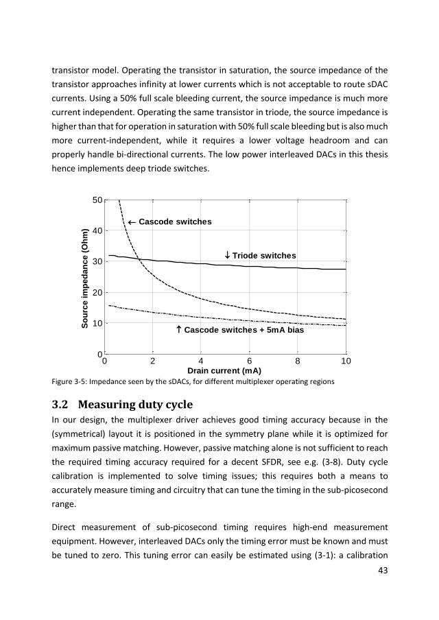
43
transistor model. Operating the transistor in saturation, the source impedance of the
transistor approaches infinity at lower currents which is not acceptable to route sDAC
currents. Using a 50% full scale bleeding current, the source impedance is much more
current independent. Operating the same transistor in triode, the source impedance is
higher than that for operation in saturation with 50% full scale bleeding but is also much
more current-independent, while it requires a lower voltage headroom and can
properly handle bi-directional currents. The low power interleaved DACs in this thesis
hence implements deep triode switches.
Figure 3-5: Impedance seen by the sDACs, for different multiplexer operating regions
3.2 Measuring duty cycle In our design, the multiplexer driver achieves good timing accuracy because in the
(symmetrical) layout it is positioned in the symmetry plane while it is optimized for
maximum passive matching. However, passive matching alone is not sufficient to reach
the required timing accuracy required for a decent SFDR, see e.g. (3-8). Duty cycle
calibration is implemented to solve timing issues; this requires both a means to
accurately measure timing and circuitry that can tune the timing in the sub-picosecond
range.
Direct measurement of sub-picosecond timing requires high-end measurement
equipment. However, interleaved DACs only the timing error must be known and must
be tuned to zero. This tuning error can easily be estimated using (3-1): a calibration
0 2 4 6 8 100
10
20
30
40
50
Cascode switches
Cascode switches + 5mA bias
Triode switches
So
urc
e i
mp
ed
an
ce
(O
hm
)
Drain current (mA)
44
signal at half the sampling frequency generates a timing spur at DC. This DC spur can
be measured and tuned to zero using e.g. an auxiliary ADC with low linearity and low
signal bandwidth. Generating this calibration signal with an interleaved DAC is
straightforward: both sDACs are placed at a constant, opposite, code. Assuming the
amplitudes of the sDACs are equal, any error in the duty cycle will result in a non-zero
DC differential output voltage level.
In practice there will be offsets in the measurement, for example due to mismatch in
the load resistors or in the ADC itself. By swapping the sDAC codes these offsets can be
cancelled, via the same principle as a chopper amplifier is based on. This also allows for
doing the calibration single-endedly instead of differential. Large variations in supply
voltage or temperature can require new calibrations to keep the duty cycle error
sufficiently small. However for small changes this is not necessary since the majority of
the variation in delay due to these variations will be common mode for the positive and
negative switch signals.
During calibration the signal is at Nyquist while the calibration attempts to remove all
spurs at DC. If also amplitude mismatch is present, this creates a spur at DC as well. The
algorithm tries to cancel this spur by introducing a duty cycle error that creates a spur
with equal size but opposite phase, cancelling out the amplitude spur.
For signals near DC, a duty cycle error has little effect while the amplitude error is
attenuated by 10dB, see (3-4). With just an amplitude error present this would decrease
to 2dB at Nyquist, see (3-5). However with increasing signal frequency, the size of the
duty cycle spur (with opposite phase compared to the amplitude spur) increases and
increasingly cancels the amplitude spur. Then the combined spur magnitude decreases
with increasing frequency; ideally at Nyquist the two spurs cancel out each other
perfectly. From this it follows that in a timing calibrated interleaved DAC the minimum
attenuation of the amplitude error spur is 10dB. This means that if a 50dB SFDR is
required, the amplitude difference between the two sDACs is allowed to be up to 1%,
or slightly over 5 LSB for a 9-bit DAC. The SFDR as function of co-existing amplitude and
timing errors is discussed more extensively in Appendix A, where also equations are
derived for the (partial) cancellation of the amplitude-mismatch induced spur by the
timing related spur.

45
Medium Speed Demonstrator:
12-bits at 1.7GS/s
In order to verify effectiveness of using the interleaved architecture presented in the
previous chapter to design a fast and accurate DAC, a 12-bit, DAC was designed in 65nm
CMOS. The goal was to design a DAC competitive with state-of-the-art in the low GS/s
range, which would - depending on the exact sampling frequency - require an SFDR of
60dB or better. For this linearity 12-bit is more than sufficient, so performance is not
limited by the number of bits, while adding more bits increases complexity for no
further gain. The realized DAC was set to operate at 1.7GS/s, to balance linearity and
sample rate in the final results.
In this chapter the designed chip and its performance is introduced, followed by a
conclusion regarding its effectiveness. This chapter is based on [65], compared to [65]
more explanations regarding the design are included while also additional
measurements results are shown.
4.1 Architecture In the designed chip, each sDAC essentially is a complete current DAC, including
separate bias sources and decoder logic. The sDACs have a 6-6 segmentation, where
the MSB sources are implemented with thermometer code and the LSB sources use
binary code. Their output current goes to the sDAC multiplexer, which alternatingly
connects one sDAC to the output, and the other one to an identical dummy output. The
resistive load consists of four 50 Ohm on-chip resistors; two single-ended loads for each
of the two differential outputs, in parallel to four 50 Ohm off-chip resistors.
46
Static matching
The current sources of the two sDACs have equal process spread, but a (largely)
uncorrelated mismatch; therefore their INL curves are also (largely) uncorrelated.
When interleaving, the difference in INL between the 2 sDACs causes an (interleaving)
output spur located at a frequency equal to the fundamental tone mirrored around half
Nyquist. The only way to eliminate this interleaving spur is to get similar (preferably
identical) INL curves for both sDACs, e.g. using calibration. For calibration purposes
small (digitally controlled) calibration current sources are included in parallel to all MSB
thermometer current sources and the two largest LSB binary scaled sources. The
smaller LSB current sources will have a sufficiently low contribution to the overall
INL/DNL of the system to not limit performance.
A conventional way to calibrate would be using a (more than) 12-bit linear ADC to
calibrate the INL of both sDACs to near zero. Since this method allows for direct,
accurate, calibration of the complete transfer curve, it prevents large INL errors due to
cumulative residual errors after calibration of current sources. However this
conventional way does require a relatively complex ADC because it needs to meet the
DAC’s high linearity requirements over the full output signal range.
The calibration for our interleaved DAC is different and requires only a low-linearity
ADC. Calibration happens at a relative low speed, so the ADC also does not need to be
fast. A faster ADC does reduce the time calibrations required. During the calibration,
first one of the sDACs is calibrated towards a sufficiently low DNL-INL and then the
second sDAC is calibrated to get the same INL behavior.
This calibration is done in two steps. Firstly to calibrate the first sDAC, each
thermometer MSB source (having a nominal weight of 64LSB) is calibrated to be equal
to all LSB sources combined (a nominal weight of 63LSB) + one extra LSB source. Now
the calibrating ADC only has to compare the value of the MSB source with a reference
value and hence the ADC only needs to be monotonic. Note that this method actually
calibrates the DNL, but due to cumulative errors the INL can still have a significant error.
Subsequently, the transfer of the second sDAC is calibrated to match the transfer of the
first sDAC by calibrating the second sDACs MSB sources.
The result is that the INL of the second sDAC follows the INL of the first one: so the
second sDAC has an INL error, but there is only a minor residual difference between the

47
INLs of the sDACs. During this calibration phase, we only have to measure the difference
between two values: again there are very low demands on the linearity of the
calibrating ADC.
Dynamic matching
In interleaved DACs, the time intervals in which each sDAC is connected to the DAC
output must be equal, otherwise spurs mirrored around half Nyquist occur, as
discussed in section 3.1.2.
From (3-8) it follows that for a full Nyquist signal at 1.7GS/s and an SFDR>70dB, the
static timing error must be smaller than 110fs. These levels of timing accuracy
practically cannot be obtained by matching only: also here calibration is required.
In our design we use a quasi-DC measurement to calibrate the timing. In it, first one of
the sDACs is set to its maximum output value while the other one is set to its minimum
value. The resulting average output voltage is dependent on the signals amplitude
(previously calibrated, see section 4.1.1) and the duty cycle of the generated square
wave. The calibration can be repeated with the first sDAC at its minimum and the
second at its maximum to further decrease mismatch effects.
4.2 Circuit implementation details An advantage of the interleaved architecture is that the sDAC design is relative simple
and straightforward. The basic current steering architecture depicted in figure 1-12, a
cascoded current source with two data switches on top of them, is used for the sDACs.
Since the MSB and two largest LSB current sources are calibrated, they do not need to
have high intrinsic matching. The unit current cells are dimensioned at 0.45μm/330μm,
with cascodes sized 0.2μm/0.15μm. They are grouped to together form the different
current sources required in the sDAC. The MSB current sources, which consist of 60 unit
sources, each have 5 smaller current sources in parallel for calibration purposes,
allowing them to be calibrated between 60 and 67.75 unit sources with steps of 1/4th
unit source. Each of these sources have an SRAM memory cell which can be
programmed via the external control bus of the chip to turn them on/off. The largest
LSB source has 4 calibration current sources, and 30 fixed unit sources, while the second
largest LSB source has 3 calibration sources and 15 fixed unit sources. The remaining
LSB’s only have fixed sources: respectively 8, 4, 2 and 1.

48
Multiplexer and driver design
The timing calibration uses the timing generation circuit in figure 4-1 to adjust the edges
of the clock signal until the duty cycle is sufficiently close to 50%. The circuit first divides
the input frequency by 2; a digitally controlled 2x6-bit capacitor bank can slightly delay
both clock signals. Finally, the two SR-latches convert the time-delayed signals to two
anti-phase square waves with a duty cycle that depends on the delay settings. The
delay-range that can be created this way is ±3.3ps, with 50fs-55fs steps.
D
D
Q
Q
1.7GHzClk
QS
R
QS
R
Clk+
Clk-
1 2 32
1 2 32
4
4
Figure 4-1: Timing generation + timing calibration circuitry
The outputs of this circuit drives both the analog multiplexer that combines the two
sDAC outputs, and the sDACs themselves. In the previous chapter the rationale for
using the multiplexer switches in triode was shown. In the demonstrated design in this
chapter, an integrated (straight forward) capacitive level shift circuit is used to create
gate drive voltages between 0.9V and 2V to operate the multiplexer transistors in
triode. This circuit is shown in figure 4-2.
Bias design
For the interleaving architecture to function properly, each sDAC should be completely
settled before its output is connected to the output. This includes the bias and (analog)
power lines. The power lines could stabilize in time with sufficiently short bondwires,
however due to uncertainty about their inductance in the used QFN package in our
demonstrator design at design time, it was instead decided to use a large amount of
decoupling capacitors to deal with disturbances. The majority of these capacitors are
poly capacitors. While these have a relative high series resistance, the interleaved

49
architecture gives them some extra time to make sure the voltage at the relevant
locations is settled in time.
Bias
Clk+
Clk-
SW+
SW-
Figure 4-2: Multiplexer level shifter
Sufficiently reducing disturbance on the bias lines by means of adding large amounts
of decoupling capacitors would be problematic from a layout perspective. The solution
used here is minimizing the capacitance on the bias lines while also minimizing the real
part of the output impedance of the bias generator: i.e. a low ohmic reference voltage
with a small parasitic capacitance. By doing so, the recovery time of disturbances on
the bias lines is minimized, yielding well settled bias voltages when the sDAC is
connected to the output.
As shown in figure 3-1 the current sources consist of two transistors, one operates as
current source, the other one as cascode to boost the output impedance. The biasing
for the current source transistors and the cascode transistors are generated by the
circuit from figure 4-3. The current source transistor is biased using a diode connected
mosfet with length equal to that of the current source transistor. A current is forced
through the mosfet 𝑀3 , generating a reference voltage. This setup can have a low
output impedance, if a sufficient amount of current is used.
A stable and fast recovering reference is also important for the cascode transistor’s gate
voltage. The cascode reference-voltage is just as the current source reference-voltage
implemented using a diode connected mosfet to allow for fast settling. However, this
is complicated since the cascode bias level needs to be a higher voltage than the current
source bias level. Three methods are used to increase the gate-source voltage of this
diode-connected transistor.

50
R1
R2
M1
M2
LVT
M3
L > Lmin
VI-source
HVT
M4
L=Lmin
Vcascode
Peak current source
Figure 4-3: Biasing circuit for the current sources
Firstly, using the reverse short channel effects of our transistors, the threshold voltage
is maximized using a minimum length devices. Secondly while all other mosfets are low-
threshold devices, this mosfet is a high-threshold device, increasing the generated
voltage further. These high-threshold devices will not match exactly with the regular
devices over PVT (Process, Voltage and Temperature) variation. However since the
exact voltage of the cascode transistors is not critical, this is acceptable in this design.
Finally the width is decreased to generate a suitable voltage. While this has a negative
influence on the output impedance of this diode-connected reference transistor, the
effect is small enough to keep the overall output resistance is sufficiently low.
For good performance it is essential the current delivered by the current sources in the
DAC core are stable. A possible source of disturbance would be from the supply lines,
even though the bias circuits have a separate supply, coupling between supply domains
could be an issue. To suppress this a peak current source has been implemented. This
current source uses 𝑅1 to generate a reference current. If 𝑀1 has a transconductance
equal to 1/𝑅2, variations in the current generated by 𝑅1, for example due to supply
variations, do not propagate to the drain voltage of 𝑀1. This drain voltage is then used
to create a stable reference current by means of 𝑀2 . The PMOS current mirror
distributes this current to the diode connected mosfets.

51
Digital circuitry
On the chip an integrated digital sine generator is included. This was designed by STM
engineers. The sine generator is capable of generating both single-tone and two-tone
test signals of varying frequencies and amplitudes. Also optionally the signal can be
dithered.
Since the 6 MSBs in the DAC core are thermometer coded, a thermometer decoder is
required to control them. Even though in the layout there is no actual matrix floorplan
used, a row/column based thermometer decoder is implemented because of its
simplicity. This decoder consists of two 3-bit thermometer decoders, one for the rows
and one for the columns. The used 3-bit thermometer decoders are drawn in figure 4-4.
Each of the 7 thermometer outputs, 𝑡0 till 𝑡6 is created from the three binary inputs 𝑏0,
𝑏1 and 𝑏3 using logic gates.
b0
b1
b2
t0b1
b2
t1 t2
b0
b2
b1
b2
t4b1
b2
t5
b0
b1
b2
b2 t3
b1
b2
t6b0
Figure 4-4: 3-bit thermometer decoder
The two 3-bit thermometer decoders are combined to create a single 6-bit
thermometer decoder, this is depicted in figure 4-5. In this figure the circuit is drawn as
a matrix for simplicity, however in the actual layout they are placed in a line. Each cell
in the matrix uses the state of its corresponding column bit, and its row bit in addition
to the next row bit, to calculate its state: A cell has a ‘high’ output when either its
column input and its row input are both ‘high’, or when the next row is ‘high’. A flip-
flop is used afterwards to reclock the signal.

52
The total thermometer decoder has 63 outputs, which in a square matrix means 8
inputs on each side. The first three binary bits are used for the column decoder. The 8th
column input is always fixed at zero, the cells in this column are only enabled when the
next row is activated. The other three inputs are used for the row decoder. Here the
first row (at the bottom in the picture) is always ‘high’, the 9th row is always ‘low’. The
last cell in the matrix, top-right, is always ‘low’. This brings the total number of
thermometer outputs at the expected 63.
rown+1
rown
columnm D Q
Q
t8n+m
t8n+m
Clk
3-bit thermometer decoder
b0 b1 b2
0
3-b
it t
he
rmom
ete
r d
ecod
er
b3
b4
b5
1
0
Figure 4-5: 6-bit thermometer decoder created using two 3-bit thermometer decoders
53
4.3 Measurement results The DAC was produced in a standard 65nm CMOS technology from ST Microelectronics.
Figure 4-6 shows the die micrograph. From it the symmetrical layout can be observed,
which is required to prevent interleaving spurs. An earlier version did not have this
symmetrical layout, which limited its performance. The resulting problems from this
earlier version are discussed in Appendix C. The active area of the demonstrator is
0.4mm2 and the chip is packaged in a standard QFN40 package. The IC consumes 70mW
from its single 1.2V supply, excluding sine generator power consumption. Parallel to
the internal 50Ω resistors, the DAC is externally loaded with 50Ω resistors, without the
customary RF chokes which are generally required for sufficient voltage headroom.
Both the internal and external resistors are connected to the 1.2V supply. The
interleaved DAC delivers 500mVpp-diff full scale swing to the outputs.
Static matching
Figure 4-7 shows the measured static INL of the two sDACs before and after calibration.
Calibration is performed using an Agilent 33401A multimeter which performs the role
of ADC, with the calibration code running on Matlab, and setting the calibration SRAM
cells using the serial bus of the chip.
Before calibration the two sDACs have different gains, resulting in a large difference in
INL between the two sDACs. After calibration the INL is significantly improved, although
the INL is still substantial because of both our rather noisy off-chip multimeter and
because we actually only calibrated the DNL; cumulative errors in the calibrated DNL
add up. Most importantly, the differential INL is minimized: the second sDAC clearly
follows the INL curve of the first sDAC curve, despite the noisy ADC. Before calibration
the best-fit full scale gain error is over 60LSB, after calibration this is less than 0.4LSB.

54
Figure 4-6: Die photograph, the complete chip size is 1.6mm x 1.6mm
Figure 4-7: a) Static INL before and b) static INL after calibration
0 1024 2048 3072 4096-50
0
50Pre-calibration INL
Code
INL
(L
SB
)
0 1024 2048 3072 4096-10
10Post-calibration INL
Code
INL
(L
SB
)
Multiplexer
sDAC-A sDAC-B
Sine generator
Δ INL
INL-BINL-A
Δ INL
b)
a)
INL-A
INL-B

55
Dynamic matching
The uncalibrated timing error was measured across 10 samples. This was done by the
same DC measurement method that was used to calibrate the timing error out,
described in section 3.2. The standard deviation of the calculated timing error of the
measured samples equals 0.66ps, with an average timing error of 0.29ps. Figure 4-8
shows the timing error measured for different digital calibration codes of the timing for
an unselected sample. For both halves of the differential switch signal, the rising edge
can be delayed in 63 digital steps, which gives a differential range of -63 to 63. The total
calibration range for the current design is 3.3ps. While this does not span the entire 3-
sigma range, from the measured values it indicates it should be sufficient for nearly
98% of the samples.
Figure 4-8: Measured timing error versus calibration code
Spectrum
The spectral performance of the DAC is shown in figure 4-9. The median SFDR over
Nyquist is 60dB, with a minimum of 58dB. The IM3 is above 62dB across Nyquist, with
a median value of 73dB. Additionally it is clear that the interleaving spur does not limit
performance; HD2 and HD3 spurs (which have different frequency dependencies)
alternatingly limit the SFDR. At Nyquist the interleaving spur is at -65dB; using (3-8) it
follows that the timing error was calibrated to around 210 fs.
-64 -48 -32 -16 0 16 32 48 64
-2
-1
0
1
2
Tim
ing
err
or
(ps
)
Differential tune code
3.3
ps
56
Figure 4-9: Spectral performance at 1.7GS/s
Figure 4-10 shows the spectrum for an output frequency of 604MHz at a sample rate
of 1.7GS/s. The figure shows that for this frequency the HD3 is dominant, and that
performance is not limited by the interleaving spur. At other frequencies the HD2 can
be dominant, the interleaving spur does not typically limit performance.
In order to demonstrate the performance improvement achieved by interleaving, the
performance of an individual sDAC was measured without interleaving using two-tone
tests. Since the single sDAC runs at half the sample rate of the complete system, the
SFDR of the two cases are hard to compare due to aliasing spurs in the output spectrum
of the single sDAC. The IM3 obtained from two-tone tests does not have this problem,
and can also be easily compared when the single sDAC is operating in its second Nyquist
zone. In figure 4-11 the IM3 of the single sDAC is plotted against the frequency and
compared to the IM3 of the complete system where interleaving is enabled. Above
425MHz the single sDAC enters its second Nyquist zone, where its performance drops
rapidly,, but also for lower frequencies it performs far worse than the complete
interleaved DAC system.
0 100 200 300 400 500 600 700 80050
60
70
80
90 Interleaving spur
IM3
SFDR
SFDR (dB)
IM3 (-dBc)
Interleaving
spur (-dBc)
Frequency (MHz)

57
Figure 4-10: Spectral plot with an output frequency of 604MHz at 1.7GS/s
This also shows that compared to a non-interleaving DAC the area and power budget
does not need to be doubled, since high performance can be achieved with two sDACs
that only have moderate performance.
Low voltage operation
The interleaved DAC circuit was designed to operate at 1.2V, and shows only a graceful
degradation of performance with lower supply voltages. The median SFDR drops by
around 5dB when the supply voltage Vsupply is lowered from 1.2V to 1V. Note that we
use a resistive load, without the customary RF chokes that would lift the DC level of Vout
to Vsupply; consequently the actual voltage at the outputs gets as low as respectively
950mV and 750mV with 500mVpp-diff swing during the measurement results
presented in this chapter. With the output voltage at 750mV the majority of this is used
to bias the current sources; the interleaving switches are designed to have a low drain-
Stop 849 MHz Start 1MHz
Fund
HD2 Interleaving spur
HD3

58
source voltage, and also the data switches operate at the edge of triode region when
the output voltage decreases to this level.
Figure 4-11: IM3 behavior with interleaving enabled and disabled at 1.7GS/s interleaved, 0.85GS/s
non-interleaved
Comparison to state-of-the-art
Figure 4-12 compares to performance obtained by this design with other state-of-the-
art designs. Compared to the other NRZ results, except [44], this design achieves
significantly better SFDR. [22] achieves a better SFDR, but this does utilize return-to-
zero, which as discussed in section 2.3.2 also has its downsides. While [15] and [34]
have a higher sampling rate and output swing, this does come at the cost of a much
higher required supply, higher power consumption and a significantly larger core size.
[55] is comparable in supply voltage and power consumption, while additionally only
requiring a very small area. However its SFDR is significantly worse.
The design of [44] achieves better linearity at a higher sample rate (although SFDR/IM3
is not over its entire Nyquist range) and with a high output current. However with over
0 100 200 300 400 500 600 700 80030
40
50
60
70
80
90
IM3 interleaved
IM3 non-interleaved
IM3 (-dBc)
Frequency (MHz)

59
30 times the power consumption and a core area which is more than 10 times larger,
the designs are in different categories.
4.4 Conclusions A high-speed interleaving DAC is presented that runs at 1.7GS/s at low supply voltages
without requiring RF chokes while achieving an SFDR across Nyquist that is better than
previous non-return-to-zero DACs with comparable power consumption and does not
have the higher clock jitter sensitivity and filtering requirements inherent to an RZ DAC.
This interleaving DAC retains the advantages of conventional current steering DACs
while the interleaving spurs that may occur when improperly interleaving are
effectively suppressed using calibration of the DNL of one sub-DAC, calibrating the
difference between the INLs of both sub-DACs to zero and calibrating the timing error
to around 210fs. This calibration method can be implemented using low-accuracy, low-
speed AD converters.
This [15] [34] [22] [55] [44]
Tech 65nm 180nm 65nm 40nm 65nm 180nm
Resolution [Bits] 12 14 12 12 9 14
Power [mW] 70 <600 188 40 60 2300
Vsupply [V] 1.2 -1.5/1.8 1.2/2.5 1.2 1.2 1.8/3.3
Area [mm2] 0.4 4 0.825 0.016 0.04 5.2
Swing [Vpp-diff] 0.5 1.0 2.5 0.8 (RZ) 0.4 80mAb
Fs [GHz] 1.7 3 2.9 1.6 3 4.6
SFDRa [dB] 58 52 52 70 49 69c
IM3a [dBc] -62.5 -65 -61 -70 -60 -74c
RZ No No No Yes No No
DEM No No No Yes No No
a. The worst-case SFDR/IM3 up to Nyquist/850MHz, whichever is lower
b. No load impedance is reported: the voltage swing is unknown
c. SFDR is reported at 500MHz, IM3 up to 1GHz
Figure 4-12: Comparison table


61
High-speed Demonstrator: 9-
bits at 8.8GS/s and 11GS/s
This chapter is based on [61], section III and sections V up to VIII. The work in [61] is
based on a 28nm FDSOI demonstration implementation, which was first published as
[66]. In addition to the 28nm implementation also a 65nm bulk CMOS variant of the
same circuit was designed and measured. This circuit was not discussed in [61], but is
included in this chapter. Despite the special characteristics of FDSOI technology, it can
largely be designed as regular bulk CMOS. Appendix D discusses some of the (potential)
advantages FDSOI offers for current steering DACs over bulk CMOS.
Compared to the design discussed in chapter 4 the demonstrators discussed here were
designed for higher operating speeds at lower accuracy. Both the 28nm and 65nm
version are 9-bit DACs employing no current source calibration and instead rely on
passive current source matching. The target linearity for both designs is above 50dB
SFDR.
In this chapter, the results of both the 28nm and the 65nm variant are presented,
together with some more in-depth analyses compared to the original paper [61]. The
65nm bulk CMOS and the 28nm FDSOI implementation are largely identical; the small
differences between the two implementations are discussed in section 5.2.

62
5.1 Suppressing code-dependent supply and bias load: Quad-
switching Due to the switching of the data-switches, both the bias line(s) and power supply line(s)
observe a code-dependent load which severely limits DAC linearity. The charge injected
into bias and supply lines due to the data-switches results in voltage variations which
modulate the output current of each sDAC slice, creating mixer-like behavior. Since the
switching action of the data-switches is code-dependent, the resulting voltage variation
on the supply and bias nodes is also code-dependent. The mixing of these signals with
the intended output signal creates unwanted harmonic distortion components.
The interleaving architecture presented in chapter 3 inherently allows settling of all
kinds of switching related issues, as long as sufficient settling is accomplished in an
sDAC before placing it on the overall DAC output. For bias and power supply lines this
would translate in requiring low-ohmic (reference) voltages without decoupling
capacitors as the latter are inherently slow2. Compared to the other nodes in high-
speed DACs, these bias and supply power lines are however still relatively slow, and a
sufficiently low-ohmic reference over a wide bandwidth would require a high power
consumption.
Hence, while interleaving suppress artifacts from code-dependent switching, extra
measures are required to decrease the code-dependent loading of bias and supply lines
in an area and power efficient way.
In the design presented in chapter 4, the sample rate was sufficiently low to allow bias
lines to settle in time using a low-ohmic reference circuit. The higher sampling rate of
this design would make the cost in power prohibitive. Chapter 4’s design did use
decoupling capacitors for the power supply, where the limited bandwidth of the poly
capacitors and routing was still acceptable for its 5-6 times lower sampling rate than
the designs discussed here.
A well-known method to decrease data-dependent behavior is using dummy structures
that switch when the main structure does not switch. This fundamentally comes at the
2 If there are no area requirements, an alternative may be to use very slow settling which effectively will make any bias and power supply line purely DC. This usually requires huge on-chip capacitances and many low-ohmic wiring which typically is not acceptable.

63
cost of extra power and extra area consumption. Using matched dummy structures to
sufficiently suppress loading effects in high-speed DACs, the increase in area and power
is roughly a factor 2.
An alternative to using dummies is quad-switching [41] [15] which uses four switches
per current source to direct the current to the positive or negative output, see e.g.
figure 5-1. Similar to dummy structures, quad-switches make sure every cycle the same
amount of switching activity occurs: regardless of the (change in) code every clock cycle
in each sDAC slice one switch will turn off and one switch will turn on. However in
contrast to a full dummy structure in parallel, quad-switching re-uses the regular
current sources, thereby only adding the extra switches and their drivers, with their
corresponding increase in area and active power. Since quad-switching structures can
be closely packed, timing matching can be better than with separate dummy structures.
Figure 5-1: Schematic of the sDAC implementation and their connections
However quad-switching also has downsides compared to using dummy structures. The
main problem is that the extra switches are directly in the signal path. The extra amount
of switches increase the likelihood of timing errors, and differences between the two
switches for one side result in spurs similar to interleaving spurs, including the high
timing demands of interleaving switches. The usual way to solve these spurs is to run
the quad-switches at twice the data rate [42]: in each sample period both switches for
the active output are toggled. In interleaving DACs however, these quad-switching
P2P1 N2 N1 N2 N1P2P1
Bias
Multiplexer
sDAC-A
6 LSB slices
7 MSB slices
sDAC-B
6 LSB slices
7 MSB slices
+ -
Out+ Out- Dummy+ Dummy-
+ -

64
spurs mentioned above are inherently suppressed in the same way as all other data
timing related errors. Static differences in output current between the different quad-
switches, for example due to differences in threshold voltage, modulating the drain
voltage of the current source, are suppressed by the output impedance of the current
sources, and are generally not an issue. This makes quad-switching very suitable to be
integrated in an interleaved architecture: the advantages of quad-switching are
obtained, while its disadvantages are inherently suppressed.
5.2 Circuit implementation details The interleaving architecture significantly simplifies the sDAC design: since most of the
dynamic errors are suppressed, the design is not as critical as that of regular DACs. As
discussed in section 3.1.1, static errors are not suppressed by interleaving but do not
have to limit performance at medium resolution and high-speed.
Figure 5-1 shows the implementation of the sDACs and their connections. Both of the
9-bit sDACs consist of 6 binary coded LSBs, and 3 thermometer coded MSBs. Quad-
switches redirect their output current to either the positive or the negative output. The
quadrature generation and switch drivers are implemented with standard core cells,
this sets the minimum the width of each sDAC slice. The driver power of these standard
cells limit the width of the data switches that can be driven by one slice. Placing
standard cells in parallel to increase the drive power is possible, but makes the layout
of the smaller slices less efficient. The maximum drive power of one slice, combined
with the preference to use as few slices as possible to reduce area and power, sets the
segmentation of the design: 6 bits are binary implemented, while the remaining 3 bits
are thermometer coded. The current source transistors of the two sDACs share a single
bias rail to improve their matching, while the bias lines of the cascode transistors are
only shared within an sDAC to improve isolation between the two sDACs.
Dynamic errors are suppressed as long as they are sufficiently died out by the time the
sDAC is connected to the output: for that, all internal nodes need to be sufficiently
settled. For errors such as sub-picosecond timing mismatch in the data switches this is
not a problem, and they will be virtually completely suppressed. For measurements,
the demonstrator chips are packaged in a standard QFN32 package. While the four 50Ω
single-ended on-chip resistors in addition to the four 50Ω off-chip resistors required for
measurements reduce the influence of the bondwires, the bondwire inductances still
prevents complete settling of the output nodes within a sampling period.

65
During operation, the sDAC that is switched to a new code is not connected to the DAC
output. Ideally the errors during this settling are fully suppressed in the interleaving
architecture. However, these settling related errors before the sDAC is placed at the
output can still propagate to the output: the multiplexer switches do not provide 100%
isolation, especially for larger current spikes. Also variation in the on-resistance of the
multiplexer switches, due to e.g. mismatch/proximity effects and due to drain current
dependencies may yield spurs in the DAC output. These latter effects decrease with
increasing sDAC output impedance.
Current sources
The current sources in the sDACs need to have a sufficiently high output impedance
and they must be well-matched. These demands are partialconflicting. Good matching
implies that the transistors must be relative large and preferably are in a common-
centroid layout. For large transistors, wide and/or long transistors must be used. Wide
transistors result in low output impedances, while long transistors result in a low
voltage headroom. Increasing matching using e.g. common-centroid techniques usually
increases the total output capacitance of current sources. In our 9b design, the current
sources are placed in a common-centroid layout. The common-centroid layout is
required to fulfill matching requirements. The 12-bit design discussed in chapter 4
employed active calibration, which removed this matching requirement for that design.
The cascode transistors are grouped together with the quad-switches and their drivers
in a line-layout to minimize parasitics, see figure 5-2. This allows the current sources to
be optimized for matching and output resistance, with a small cascode transistor to
obtain low parasitic capacitances.
In the 28nm FDSOI design this setup also resulted in sufficient inter-sDAC matching to
meet the amplitude error requirements. The larger mismatch between the sDACs in the
65nm design is compensated for by variable cascode bias voltages. The bias voltage of
the cascodes of the two sDACs can be independently adjusted per sDAC. This modulates
the drain voltage of the current sources, which modulates their current output due to
their finite output impedance.

66
Figure 5-2: sDAC layout
Switch drivers and signal generation
Proper switch signals for the quad-switching architecture are generated and buffered
in the interleaved DACs. The interleaving architecture inherently suppresses the
propagation of switching related errors to the DAC output which lowers the demand
on generation of the switch signals. Both current-mode logic (CML) drivers and CMOS
circuitry can be used to drive the quad-switches [34, 55]; both having specific
advantages and disadvantages. Quad-switching combined with interleaving removes
the need for most of the CML advantages, and using CML in combination with quad-
switching is more complicated than using CMOS drivers. In our designs, standard digital
core cells are used to generate and buffer switch signals. These are area and power
efficient, at the cost of a less than ideal switching waveform. Only in the 65nm
implementation the final set of latches to re-time the switch signals, drawn at the right
side in figure 5-3, are implemented using custom dynamic latches instead of regular
core cell latches. Dynamic latches require a clock signal to maintain their state; this
clock can be combined with/derived from the clock that is required for the analog
multiplexer. Compared to a regular core cell latch, the implemented dynamic latch
obtained better speed and lower delays, which were required for the 65nm design to
meet its stringent timing constraints.
Figure 5-3 shows the logic necessary to generate the quad-switching waveforms. The
input clock is divided by two to generate two opposite clock signals at half the main
clock frequency. A logical AND gate is used between those half-rate clocks and the
Current sources (matrix)
Switch driversCascodes andquad switches(line)

67
data/inverted data. This results in four outputs, of which only one can be high at a time.
The half-rate clocks ensures that it is never possible that one switch signal is high for
more than one single consecutive sDAC period.
The quad-switches themselves perform effectively a logical OR operator: P1 OR P2 are
equal to Data, while N1 OR N2 are equal to inverted Data. Different propagation delays
of the used cells can result in small glitches in the outputs of the AND gates. The
retiming latches suppress these glitches and output a clean signal to the switch buffers.
Data
Clk
D Q
Q
D Q
Q
A
B
A
A
B
B
P2
N1
P1
N2
D Q
E
D Q
E
D Q
E
D Q
E
Clk
Clk
Clk
Clk
B
Clk
D
A
P1
P2
N1
N2
D
D
D
Figure 5-3: Quad-switching signal generation and waveforms
Multiplexer and driver design
The analog multiplexer combines the two sDACs into a single DAC. This multiplexer
consists of 8 NMOS transistors in total, to direct the differential current of the two

68
sDACs to either the real output or the dummy output. In their on-state they are in
triode, and are dimensioned such that they add just a few ohms series resistance. This
series resistance in series with the 25Ω load resistance (the 50Ω off-chip load parallel
to the 50Ω on-chip load), ensures that both the voltage drop and the variation in the
total resistance seen by the sDACs is sufficiently small.
To drive the multiplexer transistors into triode region a capacitive level shifter is used.
This is done using the same setup as implemented in the design of chapter 4 and shown
in figure 4-2.
Tuning of the duty cycle to get a sufficient SFDR can be done in multiple ways. For
example the design discussed in chapter 4 ( [65] ) uses an array of capacitors followed
by an SR latch to adjust the duty cycle. In our 28nm FDSOI design, the backgate of the
FDSOI multiplexer transistors themselves are connected to a variable voltage source.
The wells for the transistors driven by SW+ are shared, as are those driven by SW-.
Changing the backgate voltage modulates the threshold voltage of the multiplexer
transistors which changes the turn-on and turn-off speed of the corresponding
transistors which efficiently implements duty cycle tuning. Since there is no junction
between the well and the source and drain areas, the backgates are allowed to be tuned
between 0V and 3V, which implies a differential tuning range of -3V to 3V.
The NMOS multiplexer transistors in the 65nm technology are in a regular PWELL,
which needs to be connected to ground. Deep-NWELLs can be used to isolate a PWELL
and connect it to another potential, but this would complicate the design and increase
the size of the multiplexer.
The chosen alternative for duty cycle tuning in 65nm bulk CMOS is shown in figure 5-4.
Instead of modifying the threshold voltage of the multiplexer transistors themselves,
the threshold of two PMOS transistors in the buffer can be adjusted. This
increases/decreases the slew rate of the rising edge of the output signal of the leftmost
inverter, which in turn increases/decreases the duty cycle of the drive signal for the
subsequent inverters that ensure maximum slew rate at the multiplexer inputs.
The 65nm CMOS technology is a bulk process and hence diodes are present between
bulk and the drain/source nodes. For this reason the bulk voltage may not be
significantly below the power supply voltage.

69
T+
T-
Bias
Clk+
Clk-
SW+
SW-
Figure 5-4: Multiplexer driver in the 65nm to facilitate duty cycle adjustments.
5.3 Demonstrator chip A 9-bit interleaved DAC was built in 28nm FDSOI CMOS technology; figure 5-5 shows
the die photograph, with 6 binary segmented bits and 3 thermometer bits. The
quadrature generation and switch drivers are implemented with standard core cells;
together with the switches themselves and the requirement to have each cell as narrow
as possible, this limits the maximum current that can properly be switched by each cell.
Figure 5-5: Die photograph of the DAC core in 28nm FDSOI; the core dimensions are 180μm by
220μm

70
Figure 5-6: Die photograph of the DAC core in 65nm bulk CMOS; the core dimensions are 240μm by
310μm
Compared to the DAC one discussed in chapter 4, these DACs operate at a much higher
frequency, which makes implementing a digital sine generator such as used for the DAC
from chapter 4 unrealistic. The implemented alternative is a 63-word memory for each
sDAC that provides a combined 126 word memory for test signals. Synchronization logic
makes sure that after programming the memory it will be read out in the correct order.
The 28nm implementation has an on-chip clock divide-by-two block which isolates the
internal duty cycle from possible external distortion components. For the 65nm version
this block is omitted due to speed constraints, and instead it relies on CML clock buffers
to maintain a stable duty cycle. The memory architecture is further discussed in
Appendix B.
The sDACs in the 28nm FDSOI implementation occupy approximately 0.006mm2 each,
while the total DAC core area is 0.04mm2. For the 65nm implementation the sDAC area
is approximately 0.011mm2 while the total DAC core occupies 0.075mm2, so almost a
factor two more than the 28nm version. While the unit current sources are fairly equal
in size between the two implementations, everything that switches is scaled to
minimum length in 28nm, which in turn can reduce the width while keep the
transconductance equal. A significant part of the sDACs are the standard core cells that
control the data switches; these are a lot smaller in 28nm compared to 65nm. The 28nm
DAC, excluding memory, consumes 110mW from a single 1.0V power supply source at
its nominal speed of 11GS/s, while the 65nm DAC consumes 100mW from its 1.2V
supply at 8.8GS/s. For measurement purposes the output is biased with a DC choke at
71
0.9V for the 28nm test setup and 1.0V for the 65nm test setup. A signal swing of
425mVpp-diff at DC was used during testing for the 28nm demonstrator, while the
65nm version used 400mVpp-diff swing. The extra headroom for the 65nm chip (a
slightly reduced swing combined with higher supply voltage) allowed it to extend its
better than 50dB SFDR to its entire Nyquist range.
5.4 Measurements All measurements were performed at the nominal settings described in the previous
section and after timing calibration. Timing calibration was performed manually using
the DC timing measurement method outlined in section 3.2, however it could have
been easily automated. Figure 5-7 shows the measured output spectrum for a single
tone full scale signal at 4.6GHz for the 28nm implementation with an 11GS/s sample
rate, and figure 5-8 the output spectrum of the 65nm implementation of a 3.7GHz
fundamental and a sample rate of 8.8GS/s, which for both setups is slightly above 80%
of their Nyquist frequency. Figure 5-9 shows the measured SFDR and IM3 versus output
frequency for the 28nm demonstrator, while figure 5-10 shows the similar spectrum
for the 65nm demonstrator. For each of the designs, both the SFDR and IM3 stay
respectively above 50dB and below -50dBc across Nyquist after timing calibration. At
Nyquist, the fundamental is about 5dB lower than at DC due to mainly the sinc roll-off
of the zeroth-order-hold.
Since the nonlinearities are largely due to the multiplexer transistors, the HD3 scales
with 3dB per dB increase in the fundamental and the HD2 tones scale with 2dB per dB.
This behavior is expected, since the interleaving mechanism limits the harmonics
generated by the sDACs. Due to this relationship, the amplitude which can be obtained
with an interleaved DAC with the multiplexer transistors residing in triode is limitted.
Such a limitation does not exist for the output current, and by proper impedance scaling
it is possible to increase the output power by delivering more current into a lower-
ohmic output node, e.g. via a transformer.

72
Figure 5-7: Measured output spectrum of the 28nm demonstrator with 4.6GHz full scale sine output
across Nyquist at 11GS/s
Figure 5-8: Measured output spectrum of the 65nm demonstrator with 3.71GHz full scale sine
output across Nyquist at 8.8GS/s
CLRWR
A
*
3DB
RBW 30 kHz
VBW 100 kHz
SWT 6.2 sRef 0 dBm
Center 2.755 GHz Span 5.49 GHz549 MHz/
EXTEXREF
Att 10 dB*
1 AP
-100
-90
-80
-70
-60
-50
-40
-30
-20
-10
0
1
Marker 1 [T1 ]
-10.70 dBm
4.632580000 GHz
T
Date: 20.JAN.2014 16:10:23
Fund
HD3 HD2 Interleaving
spur
10MHz 549MHz/div 5.5GHz
0dB
-20dB
-40dB
-60dB
-80dB
-100dB

73
Figure 5-9: SFDR and IM3 versus output frequency for the 28nm FDSOI IC at 11GS/s
Figure 5-10: SFDR and IM3 versus output frequency for the 65nm IC at 8.8GS/s
The sensitivity of the timing adjustment was determined using the DC timing
measurement discussed in section 3.2. In the 28nm FDSOI CMOS processes, the tuning
range of the back gates is larger than that of transistors in bulk CMOS, and is more
linear. Figure 5-11 shows the measured timing for both the 28nm FDSOI
implementation and the 65nm bulk implementation. Both implementations used a
0 1000 2000 3000 4000 500045
50
55
60
65
70
IM3
SFDR
SF
DR
(d
B)
/ IM
3 (
-dB
c)
Frequency (MHz)
0 1000 2000 3000 400045
50
55
60
65
70
IM3
SFDRSF
DR
(d
B)
/ IM
3 (
-dB
c)
Frequency (MHz)

74
tuning range of -2V to 2V differential. The 28nm FDSOI chip can accept single-ended
voltages of 0V to 3V, however above 2V linearity starts to degrade due to a too low
threshold voltage for proper operation. The 65nm implementation accepts 1V to 3V
inputs, resulting in the same differential voltage range. The better linearity of the 28nm
FDSOI timing tuning is visible, however the used implementation of the 65nm chip
results in a larger tuning range. The sensitivity of the timing adjustment is of the 28nm
FDSOI design is 1.2ps/V, while the 65nm design has a sensitivity of 1.75ps/V. The
samples measured for figure 5-11 have an uncalibrated error of 500fs and 350fs for
respectively the 28nm FDSOI and the 65nm implementation. The measured average
and standard deviation the timing error are respectively 0.65ps and 0.75ps of the 28nm
FDSOI design (based on 21 samples) and 1.2ps and 0.95ps of the 65nm design (based
on 23 samples). The error due to amplitude imbalance is included in this: it reflects the
timing shift required to fully cancel the interleaving spur at Nyquist.
Figure 5-11: Timing error for different tune voltages for the 28nm and 65nm
demonstrator designs
The gain error between the 2 sDACs of the 28nm demonstrator sample shown in the
measurement plots above was roughly 1.4LSB on the full scale output. According to (3-
4) this should result an image spur with a fundamental close to DC of 61dB. The
measured interleaving spur of this 28nm chip was at -63.5dBc for a fundamental close
-2 -1.5 -1 -0.5 0 0.5 1 1.5 2-4
-3
-2
-1
0
1
2
3
4
28nm FDSOI
65nm bulk
Tim
ing
err
or
(ps
)
Differential tune voltage (V)
75
to DC, which is a little better than the theoretical value due to the extra suppression of
the interleaving spur when the fundamental is close to DC; the interleaving spur is in
this situation located near Nyquist where bandwidth limitations will play a role. After
timing calibration, the interleaving spur does not limit performance over Nyquist. The
28nm demonstrator achieved a worst-case interleaving spur after timing calibration at
-55dBc while it was -60dBc at Nyquist. The 65nm demonstrator’s measured worst-case
interleaving spur after calibration was located at Nyquist and equal to -55dBc.
Comparison to state-of-the-art
Figure 5-12 shows a summary of the performance and a comparison with state-of-the-
art. Most notable in the comparison are the power consumption and the required area;
these are significantly lower than for most comparable designs. [55] targets similar
specifications as those shown in this chapter; they are all 9-bit, the signal swing is
identical and while [55]’s IM3 is better, its SFDR numbers are slightly worse. It requires
the same area as the 28nm version, so it is smaller than the 65nm version, and it also
requires less power. Summarized it is in those specs slightly better, the demonstrators
presented in this chapter operate at 3-4 times the clock and signal frequency compared
to the design of [55].
The work in [35] has high output power (at an unknown impedance level) and a similar
clock speed. However this comes at the cost of a higher supply voltage, higher power
consumption and a much larger die area while obtaining worse linearity. [44] is in a
similar situation, only it has much better SFDR/IM3, however this is only reported up to
a very limited frequency (respectively 500MHz and 1GHz). Also the factor 20 in power
and factor 100 in area shows this comes at a high penalty.
Just like [44], also [15] is a 14-bit design, which did publish its linearity up to Nyquist.
However despite the area and power invested in the 14-bit architecture and lower
sample rate, only in IM3 its linearity is better than our 9-bit design.
Finally [67] is an impressive design that reaches 56GS/s. It also does this with a relative
small and straightforward design, however at lower frequencies its 6-bit architecture
cannot deliver the performance of our designs.
5.5 Conclusions Two 9-bit DACs are presented that uses two-times interleaving to obtain an SFDR above
50dB across Nyquist and an IM3 below -50dB across Nyquist. The 65nm demonstrator
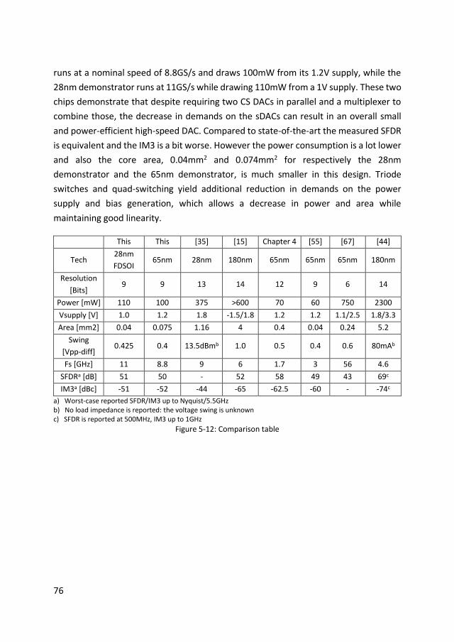
76
runs at a nominal speed of 8.8GS/s and draws 100mW from its 1.2V supply, while the
28nm demonstrator runs at 11GS/s while drawing 110mW from a 1V supply. These two
chips demonstrate that despite requiring two CS DACs in parallel and a multiplexer to
combine those, the decrease in demands on the sDACs can result in an overall small
and power-efficient high-speed DAC. Compared to state-of-the-art the measured SFDR
is equivalent and the IM3 is a bit worse. However the power consumption is a lot lower
and also the core area, 0.04mm2 and 0.074mm2 for respectively the 28nm
demonstrator and the 65nm demonstrator, is much smaller in this design. Triode
switches and quad-switching yield additional reduction in demands on the power
supply and bias generation, which allows a decrease in power and area while
maintaining good linearity.
This This [35] [15] Chapter 4 [55] [67] [44]
Tech 28nm
FDSOI 65nm 28nm 180nm 65nm 65nm 65nm 180nm
Resolution
[Bits] 9 9 13 14 12 9 6 14
Power [mW] 110 100 375 >600 70 60 750 2300
Vsupply [V] 1.0 1.2 1.8 -1.5/1.8 1.2 1.2 1.1/2.5 1.8/3.3
Area [mm2] 0.04 0.075 1.16 4 0.4 0.04 0.24 5.2
Swing
[Vpp-diff] 0.425 0.4 13.5dBmb 1.0 0.5 0.4 0.6 80mAb
Fs [GHz] 11 8.8 9 6 1.7 3 56 4.6
SFDRa [dB] 51 50 - 52 58 49 43 69c
IM3a [dBc] -51 -52 -44 -65 -62.5 -60 - -74c
a) Worst-case reported SFDR/IM3 up to Nyquist/5.5GHz b) No load impedance is reported: the voltage swing is unknown c) SFDR is reported at 500MHz, IM3 up to 1GHz
Figure 5-12: Comparison table

77
Conclusions
6.1 Summary and conclusions Chapter 1 presented an introduction into high-speed DACs, including the basics of
digital-to-analog conversions and the reasons that faster and more accurate DACs are
required. Different performance figures relevant to the presented DACs were
introduced. Finally in this chapter different types of DACs and their operation principles
were discussed.
This is followed in chapter 2 by a more in-depth look at the CS (Current steering) DAC
architecture, which is the starting point of the time-interleaved architecture. First the
limitations of the CS DAC were discussed; both its static and its dynamic limitations.
This was followed by an overview of recent literature regarding techniques to improve
CS DAC performance.
In chapter 3 the basic architecture which is used in the rest of this thesis was presented:
the two-times interleaved DAC. This interleaved DAC consists of two sDACs in parallel
of which alternatingly one is connected to the output once stabilized, while the other
one is connected to a dummy output while switching to the next output code. The
operating principle of this architecture was introduced, including how this suppresses
non-linearities of the sDACs. In the rest of chapter 3 the performance limitations of the
interleaved DAC are analyzed: mismatch between sDAC amplitude, mismatch in the
multiplexer’s duty cycle and code-dependent behavior of the multiplexer’s transistors.
A method was introduced to estimate the sub-picosecond timing error using solely DC
comparisons, which can be used to remove the timing-error using calibration.

78
This was followed in chapter 4 by a demonstrator implementation in 65nm bulk CMOS.
This 12-bit interleaved DAC operates at 1.7GS/s while achieving >58dB SFDR and
<-62dBc IM3 over Nyquist. The timing for interleaving is adjustable using a digitally
programmable capacitor bank, while a novel way to calibrate the current sources to
obtain good matching between the two sDACs was presented. Using this calibration
algorithm, the linearity requirements on the ADC used for calibration are virtually
absent while the inter-sDAC matching was shown to improve by a factor of 150. The
effectiveness of the interleaved architecture was demonstrated by comparing a single
sDAC linearity to the overall interleaved DAC performance: Besides the doubling of the
sampling rate by placing two sDACs in parallel, also IM3 performance of Nyquist is
boosted by almost 20dB. While this comes at the cost of increased power consumption
and area, since two sDACs and an analog multiplexer need to be used, the overall
system is still power and area efficient due to the low demands on the sDACs.
In chapter 5 another implementation was presented, aimed at high-speed while
maintaining reasonable linearity and only using limited area and power. The quad-
switching DAC was introduced in the interleaved architecture, where quad-switching
dramatically reduces demands on power supply and bias nodes, while the interleaved
architecture suppresses timing errors inherit to the quad-switching architecture. The
effectiveness of the design was shown by a 28nm FDSOI implementation running at
11GS/s and by a 65nm bulk CMOS implementation running at 8.8GS/s. Both achieved
>50dB SFDR and <-50dBc IM3 over Nyquist, while only using approximately 100mW.
The 28nm implementation occupied 0.04mm2 while the 65nm implementation
required 0.074mm2 die area.
Combined, in this thesis the feasibility and advantages of an interleaved DAC were
introduced, described and demonstrated. While the interleaved architecture also has
disadvantages, options were presented to deal with those disadvantages while
maintaining the advantages. It was shown that this interleaving DAC system can be used
to design high-speed DACs with good linearity and a small foot print and power
consumption.
6.2 Future work The work presented in this thesis is shown to be effective for the design of high-speed
DACs. This can be further improved upon; in the following sections some options are
discussed.

79
Signal swing
The interleaved architecture presented in this work operates best with a relatively low
output swing. With an increasing output swing, the gate-source voltage variation of the
multiplexing triode transistors also increases. At high output voltage levels, the gate-
source voltage is limited by the maximum voltage that is allowed by the used process
in order to avoid (mainly) oxide breakdown. At low output voltage levels, hence at a
low gate-source voltage, the on-resistance of the triode mosfets is large, and eventually
the mosfet will enter saturation region instead of triode which increases non-linearity.
Ideally the gate-source voltage of these transistors should be relatively constant, even
with a large output swing. This would mean the gate voltage preferably has to move
with the source voltage, and hence needs to be variable.
6.2.1.1 Bootstrap
One way to implement this is by using a bootstrap circuit that should keep the gate-
source voltage constant. However bootstrap circuits typically suffer from two
problems. The first problem is the increase in complexity: the capacitive level shifter
used in the demonstrator designs in this thesis is simple to implement, and the signal
chain is simply a string of inverters followed by a capacitor. This simplicity allows it to
operate very fast. Meanwhile a bootstrap circuit would have a lot of switches which
would need to operate in different phases.
Figure 6-1: Bootstrap circuit
The second problem is the timing of the bootstrap circuit. When bootstrap circuits are
employed in track and hold circuits for ADCs the critical edge is the edge which opens
the switch, so the edge which discharged the tracking transistor. Making this edge very
accurate timing wise is fairly straightforward. However since the DAC output is
Switch

80
continuous time, also the other edge, which closes the multiplexer switch, needs to be
accurate. This means the bootstrap transistor needs to be switched into the circuit at a
very accurate, level independent, fashion. In practice this is extremely hard to achieve.
6.2.1.2 Multiple level shifter
An alternative would be using a variable level shifter instead of a fixed one. A possible
implementation of this is shown in figure 6-2.
Figure 6-2: Variable level shifter where each capacitor is charged to a different voltage
Instead of a single capacitor that operates as a level shifter, several capacitors can be
used, each charged to a different voltage. A multiplexer chooses which of the capacitors
is used, which allows for a staircase approximation of a bootstrap output.
The resulting staircase approximation is expected to be sufficiently accurate: the
overdrive voltage of the multiplexer transistors does not need to be perfectly constant,
the goal is just to make sure they stay deep within triode region. There are also other
challenges that need to be solved with this approach: the outputs of the multiplexer
inside the level shifter experiences voltage swings outside the power supply. The
voltage levels used need to be properly synchronized with the outputs of the sDACs and
charge injection spikes that will occur when changing the shifted level are a potential
source of linearity degradation.
6.2.1.3 Transformer
A simpler solution to increase the power the DAC can deliver to its output is adding a
(wideband) transformer at the output, which can be designed to have a low swing at
its input but a high swing at its output. In order to do this a much higher current is
required, however while the interleaved architecture is limited in tolerable output
V2
Clk+ SW+
V1
S
S
V3S

81
voltage swing, increasing the output current at constant swing should not pose
problems.
An on-chip transformer has normally high losses compared to an off-chip transformer
and takes a lot of chip area. Off-chip transformers are a lot more efficient, but off-chip
components are undesired in general.
6.2.1.4 RF PA
A similar solution to the transformer option is adding an off-chip RF PA in a common-
gate/base configuration, which can present the DAC with a low impedance load,
decreasing the swing for the multiplexing transistors while still allowing a high output
swing. The downside is similar to that of a transformer: it requires an off-chip
component. An advantage compared to using a transformer is that less current is
required to get a high signal swing, simplifying the circuit design. At the same time it
does mean a higher supply voltage is required to deliver the same amount of power as
with a transformer. An extra bias current added to the signal current will be required
to keep the RF PA in its proper operating region.
Background timing calibration
Both implemented designs used foreground calibration to remove the timing error in
the analog multiplexer: At start-up the timing error was compensated, after which it
was assumed to be temperature/voltage independent. While during measurements
this has been sufficient, where the time between measurement and calibration has
been several days, a background calibration scheme that continuously corrects the
error would be advantageously.
The two implemented duty cycle adjustment methods both allow for continuous
modifications of the duty cycle. However since the measurement of the timing error is
done using a specialized waveform (square wave), this cannot be done in regular
operation.
An alternative is instead of evaluating the duty cycle at the output, to evaluate it at the
output of the final inverters in the multiplexer buffer, right before the level shifters.
From the inverted square waves the duty cycle error can be estimated with the DC
measurement method introduced in section 3.2.
A downside of this method is that errors due to differences in threshold voltage of the
multiplexer switches are not taken into account and hence are not compensated for.

82
Since introducing differences in threshold voltage is shown in chapter 5 to be effective
way to modify the duty cycle, it follows that unwanted differences can also introduce a
duty cycle error which are ignored when the measurement is done at the output of the
inverters. Whether this will be a major implementation issue will depend on the actual
circuit design, its requirements and the matching properties in the used technology.
A foreground calibration method also takes into account the amplitude error of the two
sDACs, and compensates this for near-Nyquist frequencies, this is further discussed in
Appendix A. When background calibration using the above proposed method is
implemented this does not occur, and demands on sDAC matching increase.
So it will depend on the design whether background or foreground calibration is
preferred, and more extensive research would be required to verify the concepts.
83
Appendix A
Co-existing timing and
amplitude errors
In this appendix a derivation is made for the theoretical SFDR of a two-times interleaved
DAC which suffers from both amplitude and timing mismatch. This allows for additional
insight in how these add together and how they can be used to (partially) cancel out.
Besides the amplitude and timing mismatch, no further non-idealities are included for
this derivation and an ideal zero-order hold model is used.
Initially the Fourier transform is calculated on the zero-order hold output of the two
sDACs separately, where we normalize their waveforms. Both are represented with
discrete-time domain impulse waveforms. The amplitude of sDAC-A is 1-ΔA, while that
of sDAC-B is 1+ΔA. They are centered around zero, with a normalized width of 1. sDAC-
A has a width of 1-Δt, and sDAC-B a width of 1+Δt. They are described by:
𝑓𝐴 = (1 − Δ𝐴)(𝐻 (𝑡 +1 − Δ𝑡
2) − 𝐻 (𝑡 −
1 − Δ𝑡
2))
𝑓𝐵 = (1 + Δ𝐴)(𝐻 (𝑡 +1 + Δ𝑡
2) − 𝐻 (𝑡 −
1 + Δ𝑡
2))
(A-1)
On these waveforms the Fourier transform is applied, given by:
𝐹(𝜔) = ∫ 𝑓(𝑡)𝑒−𝑗𝜔𝑡𝑑𝑡
∞
−∞
𝜔 = 2𝜋𝑓
(A-2)

84
The result is given by:
𝐹𝐴(𝑓) = (1 − Δ𝐴)sin(πf) cos(πfΔt) − cos(πf) sin(πfΔt)
𝜋𝑓
𝐹𝐵(𝑓) = (1 + Δ𝐴)sin(πf) cos(πfΔt) + cos(πf) sin(πfΔt)
𝜋𝑓
(A-3)
The wanted signal is the sum of these two transforms, while the mismatch, so the
difference, between them is the unwanted half-Nyquist mirror that needs to be
suppressed.
So the fundamental signal is:
𝐹𝑓𝑢𝑛𝑑(𝑓) = 𝐹𝐴(𝑓) + 𝐹𝐵(𝑓)
= 2sin(πf) cos(πfΔt) + ΔA cos(πf) sin(πfΔt)
𝜋𝑓
(A-4)
Since Δt is small cos(πfΔt) approaches one, and can be removed. Compared to the first
term, the second term with both a small ΔA and a small sin(πfΔt) is also neglible, which
leaves the standard zero-order hold spectrum for the fundamental, only with amplitude
2 due to the used definitions:
𝐹𝑓𝑢𝑛𝑑(𝑓) = 2sin(πf)
𝜋𝑓 (A-5)
The image frequency is the difference between the two transforms, where the
frequency needs to be taken into account: the image starts at Nyquist (f=1/2 with the
used definitions), and with increasing fundamental frequency it decreases towards DC.
𝐹𝑖𝑚𝑎𝑔𝑒(𝑓) = 𝐹𝐵 (
1
2− 𝑓) − 𝐹𝐴 (
1
2− 𝑓)
(A-6)
𝐹𝑖𝑚𝑎𝑔𝑒 (𝑓) = 2
cos(𝜋𝑓2) sin(𝜋𝑓2𝛥𝑡) + Δ𝐴 sin(𝜋𝑓2) cos(𝜋𝑓2𝛥𝑡)
𝜋𝑓2
𝑓2 =1
2− 𝑓
(A-7)

85
Since Δt is very small, the first sin can be replaced by a linear approximation, which
holds close to zero. The last cos can be removed completely, it will be very close to one.
𝐹𝑖𝑚𝑎𝑔𝑒 (𝑓) = 2
𝜋𝑓2𝛥𝑡 cos(𝜋𝑓2) + Δ𝐴 sin(𝜋𝑓2)
𝜋𝑓2 (A-8)
This can be rewritten to:
𝐴𝑠𝑖𝑛(𝑥) + 𝐵𝑐𝑜𝑠(𝑥) = √𝐴2 + 𝐵2 sin (𝑥 + 𝑎𝑡𝑎𝑛 (𝐵
𝐴)) (A-9)
𝐹𝑖𝑚𝑎𝑔𝑒(𝑓) =2
𝜋𝑓2√𝜋2𝑓2
2𝛥𝑡2 + Δ𝐴2 sin (𝜋𝑓2 + 𝑎𝑡𝑎𝑛 (𝜋𝑓2𝛥𝑡
𝛥𝐴)) (A-10)
For f = Fs/2 an amplitude error can be compensated by adding an opposite timing error.
This will be the case when the quasi-DC timing calibration is performed.
Δ𝐴 = 𝜖 Δ𝑡 = −𝜖
(A-11)
Combining these two equations:
𝐹𝑖𝑚𝑎𝑔𝑒(𝑓) = 2𝜖√1 +1
𝜋2𝑓22 sin(𝜋𝑓2 − 𝑎𝑡𝑎𝑛(𝜋𝑓2)) (A-12)
From this it follows that the magnitude of the spur is directly proportional to the error,
differences in the error will not affect the frequency transfer. So using this information
we can plot the SFDR, and know that a different ϵ will only shift the resulting graph,
and not change the shape. Below this is done for a compensated amplitude inequality
of 1%, which means 𝜖 = 0.005.

86
Figure A-1: Ideal SFDR with an amplitude inequality of 1%, compensated by duty cycle calibration
This shows that under ideal circumstances the timing calibration makes sure that the
amplitude error is worst at DC, and improves with increasing signal frequency.
0 0.1 0.2 0.3 0.4 0.540
50
60
70
80
90
100
110
120
SF
DR
(d
B)
Relative frequency (f/fs)Relative signal frequency (f/fs)
87
Appendix B
On-chip memory architecture
For testing the DACs a digital (multi-tone) sine wave is required. The 65nm 1.7GS/s DAC
from chapter 4 employs a synthesized digital sine generator for that purpose. However
while that is sufficient for those relative low speeds, the 65nm 9GS/s and the 28nm
FDSOI 11GS/s DACs from chapter 5 have a too high clock frequency to use synthesized
logic for that purpose. As alternative solution these chips use an on-chip memory which
can be programmed with the required test signals. The architecture of this memory is
discussed below.
Basic architecture The designed memory for the DAC in chapter 5 is effectively a ring-buffer which
operates at the clock speed of an sDAC. For each sDAC slice (a current source, quad-
switches and the switch signal generation and buffers), 63 D-flip-flops are placed in a
ring: every clock cycle each bit moves one position further. This architecture is shown
in figure b-1. Somewhere in the ring an extra connection is placed which moves the
data towards the quad-switching signal generation. This output connection can be
placed anywhere.
This architecture has several advantages. First of all the critical path is extremely short:
there is no logic between two flip-flops: the data only needs to be able to arrive at the
next flip-flop in time without additional delays due to logic gates. Because a ring is
made, there are some longer connections to close the circle, but the delays added due
to the longer connections are small. Since each clock cycle each bits moves one
position, the load on the power supply is virtually code independent. It does depend on
the specific digital sine loaded into the memory, but once it is loaded the same amount

88
of transitions happen each clock cycle. This reduces possible errors in the analog part
of the DAC due to power supply/ground loading, and also due to substrate noise.
The architecture also suffers from some limitations. It is very power hungry: it consist
of a lot of flip-flops which are active all the time. However since this is only used to test
the actual DAC this power consumption can be ignored as long as it does not result in
thermal problems. A larger problem is the clock distribution. Since each flip-flop needs
to move the data at the same time, also the clock needs to arrive at the same time for
each flip-flop. This means a large central clock buffer needs to provide the clock signals,
and these must be distributed to each flip-flop. This sets a limitation to the size of the
memory which can be made this way. Another limitation is that a flip-flop is a large
circuit to store a single bit: the size of the memory on the chip is also relatively large,
which is shown in figure b-2.
Because it is a repetitive pattern this can be lay-outed by hand and made suitable for
high frequency operation. The downsides means that the size of the implemented
memory is limited.
Memory implementation The implemented memory is split in two memory banks: each of the sDACs has its each
63-word memory running at opposite clock phases at half the DACs overall sample rate,
resulting in a combined 126 word memory. The output of the memory is buffered by
two more sets of flip-flops before the data is transported to the actual sDACs. The
memory runs on a separate clock from the sDACs: they are driven by the same source,
but have different delays. To prevent any timing issues between sDAC clocking and the
memory clocking there is the option to invert the clock that drives the memory;
effectively shifting the memory clock phase by half a period.
Having a 63 word memory means it is easy to connect the clocks using a binary tree,
while there are fewer sine waves which result in a repetitive pattern than with a 64
word sDAC memory.
The memories are shown in figure b-2 for the 65nm implementation. They are similar
in 28nm, however due to the tiling on that chip they are less well visible.
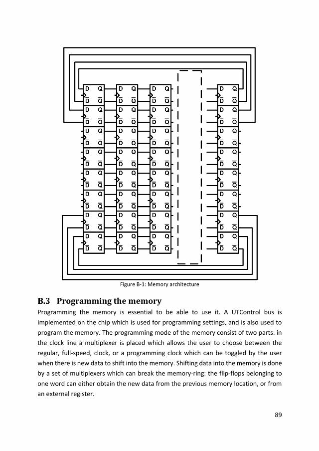
89
Figure B-1: Memory architecture
Programming the memory Programming the memory is essential to be able to use it. A UTControl bus is
implemented on the chip which is used for programming settings, and is also used to
program the memory. The programming mode of the memory consist of two parts: in
the clock line a multiplexer is placed which allows the user to choose between the
regular, full-speed, clock, or a programming clock which can be toggled by the user
when there is new data to shift into the memory. Shifting data into the memory is done
by a set of multiplexers which can break the memory-ring: the flip-flops belonging to
one word can either obtain the new data from the previous memory location, or from
an external register.

90
Figure B-2: Die photograph of the 65nm 9-bit DAC with the memories and the sDACs marked
After programming, the memory needs to revert back to regular operation. Since there
are two memory blocks these need to be correctly synced: if the memory belonging to
one sDAC starts before its turn the samples will not be reproduced in the correct order.
In order to prevent this a central block distributes the memory clock which makes sure
both blocks start in the correct phase and at the same time.
There is also another problem when it switches back to the regular clock. Figure B-3
shows this issue: if the clock multiplexer switches from programming clock to regular
clock, it is very well possible there is a small spike on the multiplexers output, which
clocks the memory. This can be interpreted as a clock edge by some flip-flips, while
others ignore it, corrupting the memory contents.
Memory-A Memory-B
sDAC-A sDAC-B

91
Clk
PClk
Program
Clk-out
Time Figure B-3: Switching from programming clock to regular clock
The circuit from Figure B-4 is designed to prevent this. The regular clock and
programming clock of both memory blocks are XOR’ed: when they are equal to each
other their output is low, otherwise it is high. A NAND gate afterwards combines these
two signals; its output is high when for both memory blocks the regular clock and the
programming clock is equal. When this happens a rising edge is generated and a flip-
flop will move the programming mode to the multiplexer settings. This means that only
when for both memory blocks the programming clock and the regular clock become
equal to each other, the clock settings can be modified, preventing short spikes on the
clock outputs.

92
D Q
ProgClk1
PClk1
Clk2
PClk2Clk-out2
Clk2
PClk2
Mux
MuxClk1
PClk1Clk-out1
Figure B-4: Clock selection circuit

93
Appendix C
Layout considerations
regarding symmetry
In this thesis the requirements regarding matching between the two sDACs has been
discussed. The importance of matching both the amplitude and the timing of the
interleaved sDACs has been shown, where mismatch causes interleaving spurs which
can limit the overall SFDR. However symmetry errors in the layout can also result in
other errors.
The 65nm 1.7GS/s DAC described in chapter 4 was actuallythe second version,
compared to the first version the layout was modified, where one of the main reasons
was to improve symmetry in the layout of the DAC. The floor plan of the original design
is shown in Figure C-1.
Problem definition In the first version the multiplexer buffer was horizontally placed near the bias of one
of the sDACs. The sDAC, including its bias, and the multiplexer buffer are connected to
different power domains, however the chip uses a shared ground, and this is a short
connection to the bias, while the connection to the other bias is a much longer
connection. This means that the disturbance on the ground line of the left bias
generator is a lot larger than that of the right bias generator.

94
Figure C-1: Floor plan of the initial design
The multiplexer buffer runs at half the overall sampling frequency. However since it is
a differential buffer the load on the shared ground line is at the full sample frequency.
If this disturbance would have been shared identically across the entire chip there
would have been no issues: the mix products of a disturbance at the full sample rate
and the fundamental signal end up at the same frequencies as regular image products.
However in this case they couple a lot stronger to one half of the interleaved DAC than
to the other half, which generates extra image frequencies which the other half does
not generate, resulting in imperfect cancellation of these images, and hence additional
interleaving spurs.
These spurs are independent of the fundamental frequency as expected: since they add
an AC modulation on the output current the amplitude of the extra generated image
frequencies do not depend on the fundamental frequency. There is a relation with the
sampling frequency, since at higher frequencies the ground is less well defined.
Because both the spur due to this layout effect and the mismatch between sDAC
amplitudes is independent of the fundamental output frequency and they occur at the
same location, it might be possible to include an extra amplitude error which could
cancel the layout induced spur.

95
Analysis Figure C-2 shows the three situations to consider. First there is the amplitude mismatch,
this we can compensate for, but we can also introduce it to counteract the two other
situations: a sine wave disturbance at the sampling frequency, with and without a 90
degrees phase shift. Other phase shifts would be a combination of these two situations.
Figure C-2: Errors due to mismatch between sDACs: a) amplitude error, b) sine disturbance at one
half, c) sine disturbance at one half with 90 degrees phase shift
To analyze this further the FFT of these signals has been taken. The most important
spectral component is the component at Fs/2, while this still falls outside Nyquist, this
component will multiply the fundamental frequency to create extra spurs inside
Nyquist. In all three situations this spur is present, which hints at the possibility of
cancelling the spur by introducing an amplitude error into the sDACs. However this is
not always an option: while all three situations do include spurs at Fs/2, the phases of
these spurs are not identical. The phase of the Fs/2 tone for cases A and C is 90 degrees.
So situation C appears to be cancellable. However the phase for case B is zero degrees:
It is orthogonal to the tone generated by A, and adding more amplitude error can only
make it worse and cannot compensate for it.
In practice the same was noticed during measurements: it was not possible to cancel
the extra interleaving spur by introducing more amplitude error. So most likely situation
B dominates this layout induced error.
Solution In the new floor plan, shown in Figure C-3, the multiplexer buffer was rotated 90
degrees, which makes the entire layout a lot more symmetrical. Since this includes the
pinout, also the PCB could be a lot more symmetrical. In the new layout the ground of
the multiplexer buffer is connected at the top side to the ground of the padring. First
of all the increased distance, with several ground connections on the padring to the
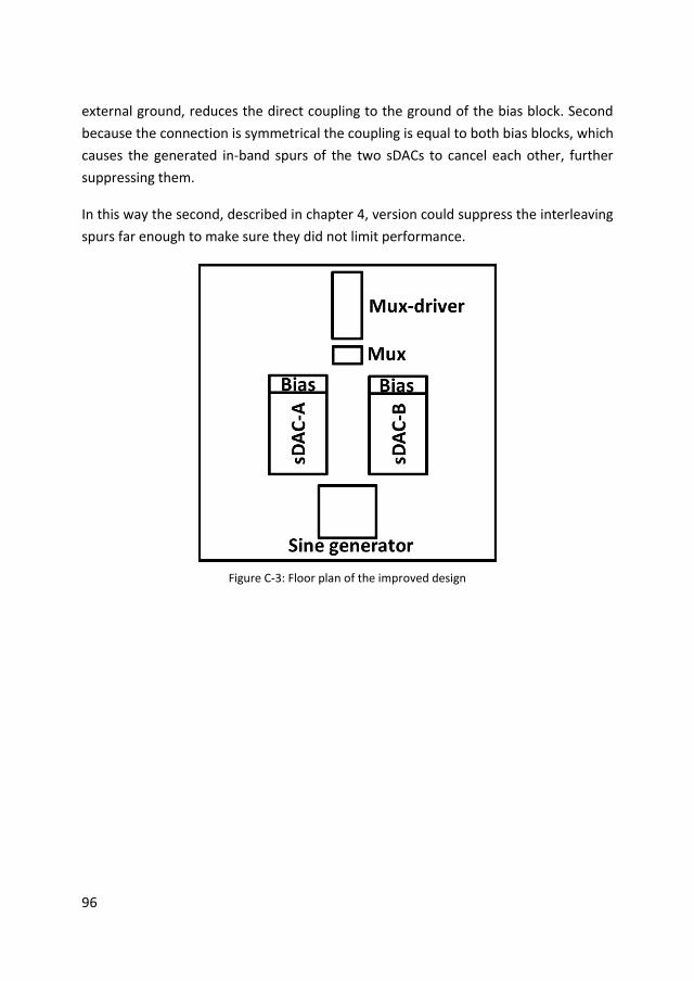
96
external ground, reduces the direct coupling to the ground of the bias block. Second
because the connection is symmetrical the coupling is equal to both bias blocks, which
causes the generated in-band spurs of the two sDACs to cancel each other, further
suppressing them.
In this way the second, described in chapter 4, version could suppress the interleaving
spurs far enough to make sure they did not limit performance.
Figure C-3: Floor plan of the improved design
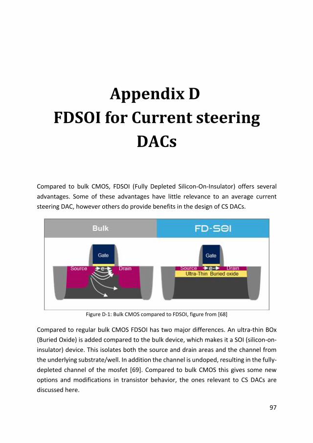
97
Appendix D
FDSOI for Current steering
DACs
Compared to bulk CMOS, FDSOI (Fully Depleted Silicon-On-Insulator) offers several
advantages. Some of these advantages have little relevance to an average current
steering DAC, however others do provide benefits in the design of CS DACs.
Figure D-1: Bulk CMOS compared to FDSOI, figure from [68]
Compared to regular bulk CMOS FDSOI has two major differences. An ultra-thin BOx
(Buried Oxide) is added compared to the bulk device, which makes it a SOI (silicon-on-
insulator) device. This isolates both the source and drain areas and the channel from
the underlying substrate/well. In addition the channel is undoped, resulting in the fully-
depleted channel of the mosfet [69]. Compared to bulk CMOS this gives some new
options and modifications in transistor behavior, the ones relevant to CS DACs are
discussed here.
98
Drain to bulk junction Regular bulk CMOS transistors have parasitic junctions from source and drain to the
bulk node. In general the capacitance of these junctions lower the obtainable speed of
circuits, and specifically for DACs the large output capacitance of current sources can
be a problem. While the ultra-thin BOx of the used FDSOI technology does not
completely eliminate this capacitance, it is greatly reduced [69].
Depending on the required specifications this might also remove the need for cascode
transistors to isolate the current source capacitance.
Output resistance Besides a low output capacitance, current sources also require a high output resistance
to approach their ideal behavior. This is especially important if a design without cascode
transistors would be implemented. FDSOI transistors have compared to bulk devices
better intrinsic gain, especially for long devices [70]. When designing current sources
this results in a higher output resistance.
Matching The channel of an FDSOI transistor does not contain dopants, which also means it is not
affected by random fluctuations of the dopant concentration. Compared to bulk CMOS
this improves device matching significantly [71]. As discussed in previous chapters of
this thesis, both current and timing matching are essential for good performance.
Depending on the available process, bulk CMOS can achieve improved matching of
current sources by employing native mosfets, however these have larger minimum
dimensions than regular mosfets, making them unsuitable for use in the dynamic
sections of a DAC.

99
Dankwoord
En dan komen we aan bij het allerlaatste stukje van dit proefschrift. Al zal het voor de
meeste lezers waarschijnlijk het allereerste stuk zijn, het dankwoord. Dit proefschrift is
uiteraard niet zonder hulp en ondersteuning van andere tot stand gekomen.
Om bij het begin te beginnen: Bedankt AJ! Als mijn dagelijks begeleider is Anne-Johan
Annema mijn eerste hulp bij ICD problemen geweest. En bij twijfels was er uiteraard
altijd de kalibratiehamer beschikbaar.
Niet de kalibratiehamer uit dit verhaal.
Vervolgens komen we automatisch bij mijn promotor, Bram Nauta. Bram heeft zowel
nuttige ideeën geleverd voor het werk zelf als ook praktische hulp. Als we het over
praktische hulp hebben dan hebben we het over de uiteindelijk bazin van ICD: Gerdien.
Zonder wiens help bij allerlei praktische problemen het AIO leven een stuk lastiger was
geweest. Natuurlijk mag ik ook Henk en Gerard niet vergeten voor hun hulp en kunde.
En niet te vergeten de andere STARS gerelateerden: Remco, Eric en Frank.
Special thanks go to Ankur Bal, Pratap Narayan Singh, Anupam Jain, Neha Bhargava,
Ranbir Singh and Nitin Chhabra. Their custom design of an integrated sine generator
greatly helped with evaluating the performance of the DAC presented in chapter 4.
More help came from STM in the form of Andreia Cathelin and Stéphane Le Tual who
presented useful feedback during the various design reviews and of course for the

100
silicon which was donated by STMicroelectronics. Also the assistance from CMP is much
appreciated.
De dagelijkse dosis aan ondersteuning, humor en tijdverdrijf is geleverd door mijn
kamergenoten: Bram, Mark, Michiel, Jasper, David, Harish, Johan, Inês en Yuan-Ching.
En speciale dank gaat naar Hugo en Dirk-Jan, die niet alleen in het kamergenoten rijtje
thuishoren, maar daarnaast ook als paranymphen hebben geholpen bij de laatste
loodjes.
Naast onze kamer was er nog een kamer die belangrijk is geweest tijdens mijn AIO tijd,
de koffiekamer. Geen wereldprobleem was te groot om ver genoeg versimpeld te
worden zodat er oplossingen bedacht konden worden (niet altijd even praktische
oplossingen overigens, maar dat is ook niet de bedoeling in de academische wereld).
Allemaal werd dat mogelijk gemaakt door de mede bewoners van de koffiekamer: Ray,
Tom, TomTom, Sander, Jurriaan, Remke, Dirk en nog vele andere permanente en
tijdelijke koffiekamerbewoners.
Als laatste, maar zeker niet als minste, wil ik ook mijn familie, en specifiek mijn ouders,
bedanken voor hun steun tijdens zowel mijn carrière als PhD’er.

101
Bibliography
[1] 2010. [Online]. Available: http://starsproject.nl/.
[2] I. Kuon and J. Rose, "Measuring the Gap Between FPGAs and ASICs," Computer-Aided Design of Integrated Circuits and Systems, IEEE Transactions on, vol. 26, no. 2, pp. 203-215, Feb 2007.
[3] E. Lee and P. Gulak, "A CMOS field-programmable analog array," Solid-State Circuits, IEEE Journal of, vol. 26, no. 12, pp. 1860-1867, Dec 1991.
[4] "AN231E04 Datasheet Rev 1.2," 2014. [Online]. Available: http://www.anadigm.com/_doc/DS231000-U001.pdf.
[5] S. Balasubramanian and W. Khalil, "Direct digital-to-RF digital-to-analogue converter using image replica and nonlinearity cancelling architecture," Electronics Letters, vol. 46, no. 14, pp. 1030-1032, July 2010.
[6] N. Friedman, The Naval Institute Guide to World Naval Weapon Systems, Naval Institute Press, 2006, p. 265.
[7] E. Vittoz, "Low-power design: ways to approach the limits," in Solid-State Circuits Conference, 1994. Digest of Technical Papers. 41st ISSCC., 1994 IEEE International, 1994.
[8] Y.-H. Kim and H. Yu, "Automatic tuning circuit for Gm-C filters," in Electronics, Circuits and Systems, 2005. ICECS 2005. 12th IEEE International Conference on, 2005.
[9] S. Smith, The Scientist and Engineer's Guide to Digital Signal Processing, California Technical Publishing, 1997.
[10] M. Skolnik, Radar Handbook, 3rd ed., McGraw-Hill, 1990.
[11] S. Cripps, RF power amplifiers for wireless communications, 2nd ed., Artech House, Incorporated, 2006.
[12] J. Velner, E. Klumperink, B. Nauta and F. van Vliet, "Multi-band linear chirp generation based on a type-III PLL," in Microwave Symposium Digest (IMS), 2013 IEEE MTT-S International, 2013.

102
[13] F. Maloberti, Data Converters, Springer, 2007, pp. 254-255.
[14] M. Oude Alink, A. Kokkeler, E. Klumperink, K. Rovers, G. Smit and B. Nauta, "Spurious-Free Dynamic Range of a Uniform Quantizer," Circuits and Systems II: Express Briefs, IEEE Transactions on, vol. 56, no. 6, pp. 434-438, June 2009.
[15] G. Engel, S. Kuo and S. Rose, "A 14b 3/6GHz current-steering RF DAC in 0.18 um CMOS with 66dB ACLR at 2.9GHz," in Solid-State Circuits Conference Digest of Technical Papers (ISSCC), 2012 IEEE International, 2012.
[16] R. Walden, "Analog-to-digital converter survey and analysis," Selected Areas in Communications, IEEE Journal on, vol. 17, no. 4, pp. 539-550, April 1999.
[17] R. Schreier and G. Temes, Understanding Delta-Sigma Data Converters, New York: Wiley, 2005.
[18] A. Ali, A. Morgan, C. Dillon, G. Patterson, S. Puckett, P. Bhoraskar, H. Dinc, M. Hensley, R. Stop, S. Bardsley, D. Lattimore, J. Bray, C. Speir and R. Sneed, "A 16-bit 250-MS/s IF Sampling Pipelined ADC With Background Calibration," Solid-State Circuits, IEEE Journal of, vol. 45, no. 12, pp. 2602-2612, Dec 2010.
[19] D. Baranauskas and D. Zelenin, "A 0.36W 6b up to 20GS/s DAC for UWB Wave Formation," in Solid-State Circuits Conference, 2006. ISSCC 2006. Digest of Technical Papers. IEEE International, 2006.
[20] "Low-power 14-bit current steering DAC, for ADSL2+/CO applications in 0.13 um CMOS," in Solid-State Circuits Conference, 2004. ESSCIRC 2004. Proceeding of the 30th European, 2004.
[21] R.-L. Chen and S.-J. Chang, "A 6-bit Current-Steering DAC With Compound Current Cells for Both Communication and Rail-to-Rail Voltage-Source Applications," Circuits and Systems II: Express Briefs, IEEE Transactions on, vol. 59, no. 11, pp. 746-750, Nov 2012.
[22] W.-T. Lin and T.-H. Kuo, "A 12b 1.6GS/s 40mW DAC in 40nm CMOS with >70dB SFDR over entire Nyquist bandwidth," in Solid-State Circuits Conference Digest of Technical Papers (ISSCC), 2013 IEEE International, 2013.
[23] J. Wikner, Studies on CMOS Digital-to-Analog Converters, Linköping University Electronic Press, 2000.
[24] K. Doris, A. van Roermund and D. Leenaerts, Wide-Bandwidth High Dynamic Range D/A Converters, Springer, 2006.
[25] J. McCreary and P. Gray, "All-MOS Charge Redistribution Analog-to-Digital Conversion Techniques-Part I," Solid-State Circuits, IEEE Journal of, vol. 10, no. 6, pp. 371-379, Dec 1975.
[26] R. Suarez, P. Gray and D. Hodges, "All-MOS charge-redistribution analog-to-digital conversion techniques. II," Solid-State Circuits, IEEE Journal of, vol. 10, no. 6, pp. 379-385, Dec 1975.

103
[27] L. Wang, Y. Fukatsu and K. Watanabe, "A CMOS R-2R ladder digital-to-analog converter and its characterization," in Instrumentation and Measurement Technology Conference, 2001. IMTC 2001. Proceedings of the 18th IEEE, 2001.
[28] K. Poulton, B. Jewett and J. Liu, "A 7.2-GSa/s, 14-bit or 12-GSa/s, 12-bit DAC in a 165-GHz fT BiCMOS process," in VLSI Circuits (VLSIC), 2011 Symposium on, 2011.
[29] M. Pelgrom, "A 10-b 50-MHz CMOS D/A converter with 75Ohm buffer," Solid-State Circuits, IEEE Journal of, vol. 25, no. 6, pp. 1347-1352, Dec 1990.
[30] A. Bugeja, B.-S. Song, P. Rakers and S. Gillig, "A 14-b, 100-MS/s CMOS DAC designed for spectral performance," Solid-State Circuits, IEEE Journal of, vol. 34, no. 12, pp. 1719-1732, December 1999.
[31] S. Luschas and H.-S. Lee, "Output impedance requirements for DACs," in Circuits and Systems, 2003. ISCAS '03. Proceedings of the 2003 International Symposium on, 2003.
[32] A. D. A. W. M.J.M Pelgrom, "Matching properties of MOS transistors," Solid-State Circuits, IEEE Journal of, vol. 24, no. 5, pp. 1433-1439, October 1989.
[33] M. Kosunen and K. Halonen, "Sampling jitter and power supply interference in current-steering D/A converters," in Circuit Theory and Design, 2005. Proceedings of the 2005 European Conference on, 2005.
[34] C.-H. Lin, F. van der Goes, J. a. M. J. Westra, Y. Lin, E. Arslan, E. Ayranci, X. Liu and K. Bult, "A 12 bit 2.9 GS/s DAC With IM3 60 dBc Beyond 1 GHz in 65 nm CMOS," Solid-State Circuits, IEEE Journal of, vol. 44, no. 12, pp. 3285-3293, Dec 2009.
[35] B. C. T. Y. K. N.-Y. W. X. C. T.-H. C. K. R. H.-F. C. R. G. J. C. J. Xiao, "A 13-Bit 9GS/s RF DAC-based broadband transmitter in 28nm CMOS," pp. C262-C263, June 2013.
[36] A. Bugeja and S. B.-S., "A self-trimming 14-b 100-MS/s CMOS DAC," Solid-State Circuits, IEEE Journal of, vol. 35, no. 12, pp. 1841-1852, December 2000.
[37] W.-H. Tseng, C.-W. Fan and J.-T. Wu, "A 12b 1.25GS/s DAC in 90nm CMOS with > 70dB SFDR up to 500MHz," in Solid-State Circuits Conference Digest of Technical Papers (ISSCC), 2011 IEEE International, 2011.
[38] W.-H. Tseng, J.-T. Wu and Y.-C. Chu, "A CMOS 8-Bit 1.6-GS/s DAC With Digital Random Return-to-Zero," Circuits and Systems II: Express Briefs, IEEE Transactions on, vol. 58, no. 1, pp. 1-5, Jan 2011.
[39] W.-T. Lin, H.-Y. Huang and T.-H. Kuo, "A 12-bit 40 nm DAC Achieving SFDR > 70 dB at 1.6 GS/s and IMD < –61dB at 2.8 GS/s With DEMDRZ Technique," Solid-State Circuits, IEEE Journal of, vol. 49, no. 3, pp. 708-717, March 2014.
[40] K. Nguyen, R. Adams and K. Sweetland, "A 113 dB SNR oversampling sigma-delta DAC for CD/DVD application," Consumer Electronics, IEEE Transactions on, vol. 44, no. 3, pp. 1019-1023, Aug 1998.

104
[41] S. Park, G. Kim, S.-C. Park and W. Kim, "A digital-to-analog converter based on differential-quad switching," Solid-State Circuits, IEEE Journal of, vol. 37, no. 10, pp. 1335-1338, Oct. 2002.
[42] B. Schafferer and R. Adams, "A 3V CMOS 400mW 14b 1.4GS/s DAC for multi-carrier applications," in Solid-State Circuits Conference, 2004. Digest of Technical Papers. ISSCC. 2004 IEEE International, 2004.
[43] S. Wan, Z. Chen, Z. Yu, S. Huang and H. Ji, "An embedded 14-bit 800MS/s DAC for direct digital frequency synthesizer in 0.18-um CMOS," in Applied Superconductivity and Electromagnetic Devices, 2009. ASEMD 2009. International Conference on, 2009.
[44] B. Brandt, D. McMahill, M. Wu, P. Kalthoff, A. Kuckreja and G. Ostrem, "A 14b 4.6GS/s RF DAC in 0.18 um CMOS for cable head-end systems," in Solid-State Circuits Conference Digest of Technical Papers (ISSCC), 2014 IEEE International, 2014.
[45] S. Balasubramanian, G. Creech, J. Wilson, S. M. Yoder, J. J. McCue, M. Verhelst and W. Khalil, "Systematic Analysis of Interleaved Digital-to-Analog Converters," Circuits and Systems II: Express Briefs, IEEE Transactions on, vol. 58, no. 12, pp. 882-886, Dec 2011.
[46] X. Li, Q. Wei, Z. Xu, J. Liu, H. Wang and H. Yang, "A 14 Bit 500 MS/s CMOS DAC Using Complementary Switched Current Sources and Time-Relaxed Interleaving DRRZ," Circuits and Systems I: Regular Papers, IEEE Transactions on, vol. 61, no. 8, pp. 2337-2347, Aug 2014.
[47] G. Radulov, P. Quinn, P. Harpe, H. Hegt and A. van Roermund, "Parallel current-steering D/A Converters for Flexibility and Sma," in Circuits and Systems, 2007. ISCAS 2007. IEEE International Symposium on, 2007.
[48] D. Feng, S. Sin, E. Bonizzoni and F. Maloberti, "Time interleaved current steering DAC for ultra-high conversion rate," in Microelectronics and Electronics (PRIME), 2014 10th Conference on Ph.D. Research in, 2014.
[49] F. Y. H.-F. Y. N. L. J. X. J.-Y. R. L. Cheng, "Nyquist-rate time-interleaved current-steering DAC with dynamic channel matching," in Circuits and Systems (ISCAS), 2011 IEEE International Symposium on, 2011.
[50] D. Aksin, G. Ozbek and F. Maloberti, "Multi-rate segmented time-interleaved current steering DAC with unity-elements sharing," in Circuits and Systems (ISCAS), Proceedings of 2010 IEEE International Symposium on, 2010.
[51] L. Cheng, F. Ye, H.-F. Yang, N. Li, J. Xu and J.-Y. Ren, "Nyquist-rate time-interleaved current-steering DAC with dynamic channel matching," in Circuits and Systems (ISCAS), 2011 IEEE International Symposium on, 2011.
[52] K. Doris, J. Briaire, D. Leenaerts, M. Vertreg and A. van Roermund, "A 12b 500MS/s DAC with >70dB SFDR up to 120MHz in 0.18 um CMOS," in Solid-State

105
Circuits Conference, 2005. Digest of Technical Papers. ISSCC. 2005 IEEE International, 2005.
[53] X. Wu, P. Palmers and M. Steyaert, "A 130 nm CMOS 6-bit Full Nyquist 3 GS/s DAC," Solid-State Circuits, IEEE Journal of, vol. 43, no. 11, pp. 2396-2403, Nov 2008.
[54] J. Deveugele and M. Steyaert, "A 10-bit 250-MS/s binary-weighted current-steering DAC," Solid-State Circuits, IEEE Journal of, vol. 41, no. 2, pp. 320-329, Feb 2006.
[55] S. Tual, P. Singh, A. Bal and C. Garnier, "A 3GS/s, 9b, 1.2V single supply, pure binary DAC with >50dB SFDR up to 1.5GHz in 65nm CMOS," in VLSI Circuits (VLSIC), 2011 Symposium on, 2011.
[56] S. Su, T. Tsai, P. Sharma and M.-W. Chen, "A 12-bit hybrid DAC with 8GS/s unrolled pipeline delta-sigma modulator achieving >75dB SFDR over 500MHz in 65nm CMOS," in VLSI Circuits Digest of Technical Papers, 2014 Symposium on, 2014.
[57] W.-T. Lin and T.-H. Kuo, "A Compact Dynamic-Performance-Improved Current-Steering DAC With Random Rotation-Based Binary-Weighted Selection," Solid-State Circuits, IEEE Journal of, vol. 47, no. 2, pp. 444-453, Feb 2012.
[58] T. Chen and G. Gielen, "A 14-bit 200-MHz Current-Steering DAC With Switching-Sequence Post-Adjustment Calibration," Solid-State Circuits, IEEE Journal of, vol. 42, no. 11, pp. 2386 -2394, November 2007.
[59] H. Van de Vel, J. Briaire, C. Bastiaansen, P. van Beek, G. Geelen, H. Gunnink, Y. Jin, M. Kaba, K. Luo, E. Paulus, B. Pham, W. Relyveld and P. Zijlstra, "A 240mW 16b 3.2GS/s DAC in 65nm CMOS with <-80dBc IM3 up to 600MHz," in Solid-State Circuits Conference Digest of Technical Papers (ISSCC), 2014 IEEE International, 2014.
[60] S.-S. Chen, N.-S. Kim and J. Rabaey, "A 10b 600MS/s multi-mode CMOS DAC for multiple Nyquist zone operation," in VLSI Circuits (VLSIC), 2011 Symposium on, 2011.
[61] E. Olieman, A.-J. Annema and B. Nauta, "An Interleaved Full Nyquist High-Speed DAC Technique," Solid-State Circuits, IEEE Journal of, vol. 3, no. 50, pp. 704-713, 2015.
[62] J. Deveugele, P. Palmers and M. Steyaert, "Parallel-path digital-to-analog converters for Nyquist signal generation," Solid-State Circuits, IEEE Journal of, vol. 39, no. 7, pp. 1073-1082, July 2004.
[63] M. Clara, W. Klatzer, D. Gruber, A. Marak, B. Seger and W. Pribyl, "A 1.5V 13bit 130-300MS/s self-calibrated DAC with active output stage and 50MHz signal bandwidth in 0.13um CMOS," in Solid-State Circuits Conference, 2008. ESSCIRC 2008. 34th European, 2008.
106
[64] D. Spicer and A. Rodger, "Antiglitch Digital to Analog Converter System". United states Patent 3,877,023, 8 April 1975.
[65] E. Olieman, A.-J. Annema, B. Nauta, A. Bal and P. Singh, "A 12b 1.7GS/s two-times interleaved DAC with <-62dBc IM3 across Nyquist using a single 1.2V supply," in Solid-State Circuits Conference (A-SSCC), 2013 IEEE Asian, Singapore, 2013.
[66] E. Olieman, A.-J. Annema and B. Nauta, "A 110mW, 0.04mm2, 11GS/s 9-bit interleaved DAC in 28nm FDSOI with >50dB SFDR across Nyquist," in VLSI Circuits (VLSIC), 2011 Symposium on, 2014.
[67] Y. Greshishchev, D. Pollex, S.-C. Wang, M. Besson, P. Flemeke, S. Szilagyi, J. Aguirre, C. Falt, N. Ben-Hamida, R. Gibbins and P. Schvan, "A 56GS/S 6b DAC in 65nm CMOS with 256x6b memory," in Solid-State Circuits Conference Digest of Technical Papers (ISSCC), 2011 IEEE International, 2011.
[68] STMicroelectronics, "FD-SOI," [Online]. Available: http://www.st.com/web/en/about_st/learn_fd-soi.html.
[69] P. Magarshack, P. Flatresse and G. Cesana, "UTBB FD-SOI: A process/design symbiosis for breakthrough energy-efficiency," in Design, Automation Test in Europe Conference Exhibition (DATE), 2013, 2013.
[70] P. Magarshack, FD-SOI: From Successful Collaborative R&D to Successful Silicon Results, 2013.
[71] X. Federspiel, D. Angot, M. Rafik, F. Cacho, A. Bajolet, N. Planes, D. Roy, M. Haond and F. Arnaud, "28nm node bulk vs FDSOI reliability comparison," in Reliability Physics Symposium (IRPS), 2012 IEEE International, 2012.
107
List of Publications
1. E. Olieman, A.-J. Annema, B. Nauta, A. Bal and P. Singh, "A 12b 1.7GS/s two-
times interleaved DAC with <-62dBc IM3 across Nyquist using a single 1.2V
supply," Solid-State Circuits Conference (A-SSCC), 2013 IEEE Asian, pp.81-84,
11-13 Nov. 2013
2. E. Olieman, A.-J. Annema and B. Nauta, "A 110mW, 0.04mm2, 11GS/s 9-bit
interleaved DAC in 28nm FDSOI with >50dB SFDR across Nyquist", VLSI Circuits
(VLSIC), 2011 Symposium on, pp. 206-207, 11-13 June 2014
3. E. Olieman, A.-J. Annema and B. Nauta, "An Interleaved Full Nyquist High-
Speed DAC Technique," Solid-State Circuits, IEEE Journal of, vol. 3, no. 50, pp.
704-713, 2015.


109
List of Abbreviations
ADC Analog-to-Digital Converter ASIC Application-Specific Integrated Circuit BOx Buried Oxide BW BandWidth CE Constant Envelope CML Current Mode Logic CMOS Complementary Metal-Oxide Semiconductor CPU Central Processing Unit CS Current steering DAC Digital-to-Analog Converter DC Direct Current DMRZ Dynamic-element-Matching and Return-to-Zero DNL Differential Non-Linearity DRRZ Digital Random Return-to-Zero DSP Digital Signal Processor FDSOI Fully Depleted Silicon-On-Insulator FoM Figure-of-Merit FPAA Field-Programmable Analog Array FPGA Field-Programmable Gate Array IF Intermediate Frequency IM3 Third-Order Inter-Modulation INL Integral Non-Linearity NMOS N-type Metal-Oxide Semiconductor NRZ Non-Return-to-Zero PMOS P-type Metal-Oxide Semiconductor RZ Return-to-Zero sDAC sub-DAC SFDR Spurious-Free Dynamic Range SNR Signal-to-Noise Ratio GS/s Giga-samples per second