Embed Size (px)
Citation preview
UCC28180
TLV3202 TLV70433 TMP302
UCC256301
TIDA-01503 AUX
UCC24612-2
OPTO TL103WA INA181
UCC24612-2
24 V/ 20 A
CSD19501
CSD19501
85 V 265V AC Mains
Copyright © 2017, Texas Instruments Incorporated
1TIDUDF3–October 2017Submit Documentation Feedback
Copyright © 2017, Texas Instruments Incorporated
24-V, 480-W Nominal, 720-W Peak, >93.5% Efficient, AC/DC IndustrialPower Supply Reference Design
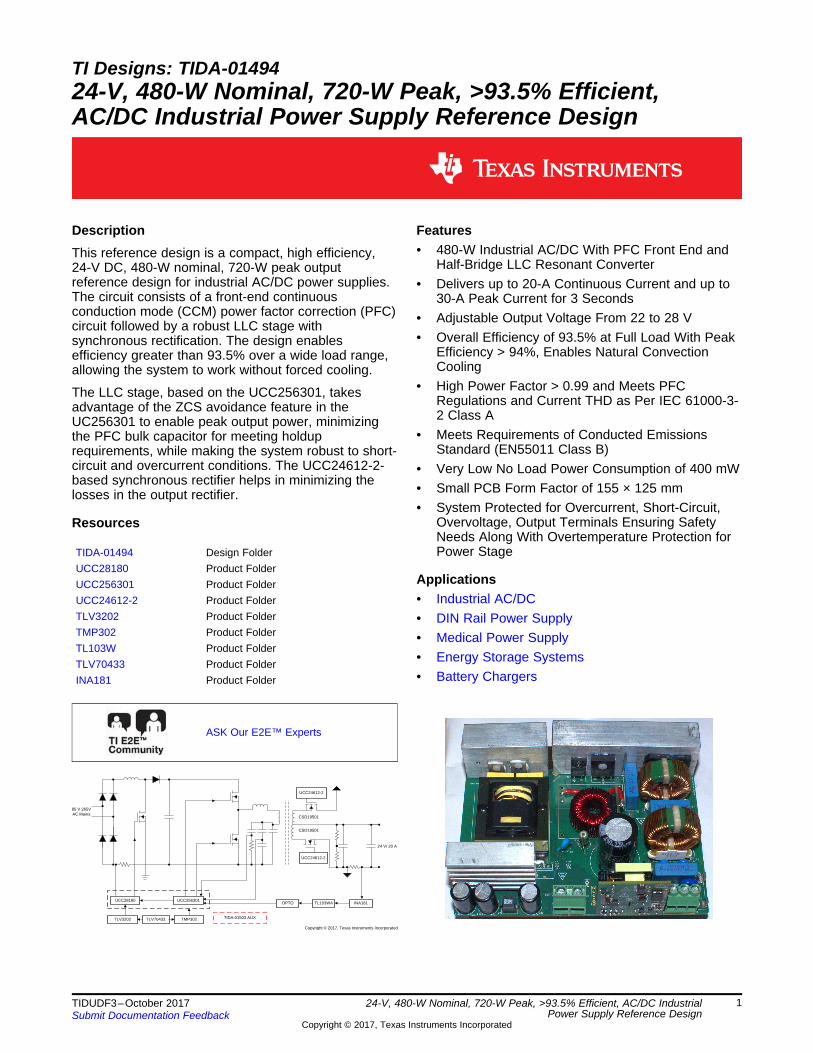
TI Designs: TIDA-0149424-V, 480-W Nominal, 720-W Peak, >93.5% Efficient,AC/DC Industrial Power Supply Reference Design
DescriptionThis reference design is a compact, high efficiency,24-V DC, 480-W nominal, 720-W peak outputreference design for industrial AC/DC power supplies.The circuit consists of a front-end continuousconduction mode (CCM) power factor correction (PFC)circuit followed by a robust LLC stage withsynchronous rectification. The design enablesefficiency greater than 93.5% over a wide load range,allowing the system to work without forced cooling.
The LLC stage, based on the UCC256301, takesadvantage of the ZCS avoidance feature in theUC256301 to enable peak output power, minimizingthe PFC bulk capacitor for meeting holduprequirements, while making the system robust to short-circuit and overcurrent conditions. The UCC24612-2-based synchronous rectifier helps in minimizing thelosses in the output rectifier.
Resources
TIDA-01494 Design FolderUCC28180 Product FolderUCC256301 Product FolderUCC24612-2 Product FolderTLV3202 Product FolderTMP302 Product FolderTL103W Product FolderTLV70433 Product FolderINA181 Product Folder
ASK Our E2E™ Experts
Features• 480-W Industrial AC/DC With PFC Front End and
Half-Bridge LLC Resonant Converter• Delivers up to 20-A Continuous Current and up to
30-A Peak Current for 3 Seconds• Adjustable Output Voltage From 22 to 28 V• Overall Efficiency of 93.5% at Full Load With Peak
Efficiency > 94%, Enables Natural ConvectionCooling
• High Power Factor > 0.99 and Meets PFCRegulations and Current THD as Per IEC 61000-3-2 Class A
• Meets Requirements of Conducted EmissionsStandard (EN55011 Class B)
• Very Low No Load Power Consumption of 400 mW• Small PCB Form Factor of 155 × 125 mm• System Protected for Overcurrent, Short-Circuit,
Overvoltage, Output Terminals Ensuring SafetyNeeds Along With Overtemperature Protection forPower Stage
Applications• Industrial AC/DC• DIN Rail Power Supply• Medical Power Supply• Energy Storage Systems• Battery Chargers
System Description www.ti.com
2 TIDUDF3–October 2017Submit Documentation Feedback
Copyright © 2017, Texas Instruments Incorporated
24-V, 480-W Nominal, 720-W Peak, >93.5% Efficient, AC/DC IndustrialPower Supply Reference Design
An IMPORTANT NOTICE at the end of this TI reference design addresses authorized use, intellectual property matters and otherimportant disclaimers and information.
1 System DescriptionIndustrial AC/DC power supplies are used in various applications such as process control, data logging,machinery control, instrumentation, factory automation, and security systems. These AC/DC suppliesprovide a convenient means for powering DC operated devices including programmable logic controllers(PLCs), sensors, transmitters and receivers, analyzers, motors, actuators, solenoids, relays, and so on.These supplies are convection cooled and need to support features like power boost where it supplies aincreased output load for a short duration. The supplies operate over a wide input range from 85- to 265-VAC, delivering full load for entire input voltage range. The output voltages from these supplies range from5 to 56 V with power ratings from 7.5 to 480 W. Many of these supplies can be connected in parallel forhigher power applications.
This reference design is a 480-W high efficiency industrial AC/DC power supply. The design consists of aCCM boost PFC converter, which operates from an input voltage range of 85- to 265-V AC RMS andgenerates a 390-V DC bus. The second stage is made up of an isolated half-bridge LLC stage, whichgenerates a 24-V, 20-A nominal output. The output voltage range is settable from 22 to 28 V usingpotentiometer present on the board. Industrial power supplies have requirements of high efficiency overtheir entire operating voltage range and wide load variations from a 50% to 100% load. This designdemonstrates high efficiency operation in a small form factor (155 × 125 mm) and delivers continuous480 W of power over the entire input operating voltage range from 85- to 265-V AC. It gives an efficiencyof > 93.5% for 230-V AC nominal operation and 91% for 115-V AC nominal operation. The CCM PFCstage is controlled by the UCC28180 fixed frequency PFC device. CCM PFC offers a cost-optimizedsolution at this power level and wide input range. The HB-LLC power stage is controlled through the stageof the art UCC256301 resonant controller, which implements current mode control for increased controlbandwidth. This increased control bandwidth reduces the output capacitors required to suppress the ACripple on the output. To achieve high efficiency, the output of the LLC stage uses synchronous rectificationbased on the UCC24612 device and the CSD19501KCS MOSFET.
The design has low standby power of < 400 mW and meets ENERGY STAR® rating requirements as wellas 2013 EU eco-design directive ErP Lot 6. The EMI filter is designed to meet EN55011 class-Bconducted emission levels. The design is fully tested and validated for various parameters such asregulation, efficiency, EMI signature, output ripple, startup, and switching stresses. Overall, the designmeets the key challenges of industrial power supplies to provide safe and reliable power with allprotections built in, while delivering high performance with low power consumption and low bill of material(BOM) cost.
www.ti.com System Description
3TIDUDF3–October 2017Submit Documentation Feedback
Copyright © 2017, Texas Instruments Incorporated
24-V, 480-W Nominal, 720-W Peak, >93.5% Efficient, AC/DC IndustrialPower Supply Reference Design
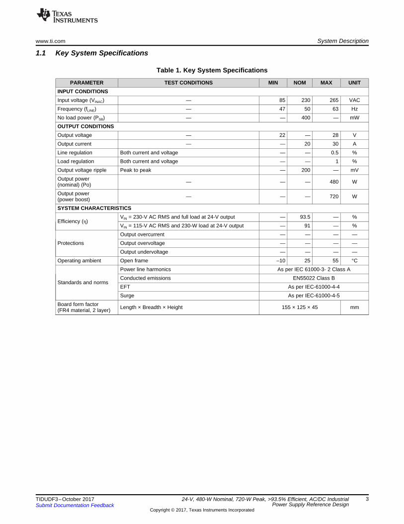
1.1 Key System Specifications
Table 1. Key System Specifications
PARAMETER TEST CONDITIONS MIN NOM MAX UNITINPUT CONDITIONSInput voltage (VINAC) — 85 230 265 VACFrequency (fLINE) — 47 50 63 HzNo load power (PSB) — — 400 — mWOUTPUT CONDITIONSOutput voltage — 22 — 28 VOutput current — — 20 30 ALine regulation Both current and voltage — — 0.5 %Load regulation Both current and voltage — — 1 %Output voltage ripple Peak to peak — 200 — mVOutput power(nominal) (Po) — — — 480 W
Output power(power boost) — — — 720 W
SYSTEM CHARACTERISTICS
Efficiency (η)VIN = 230-V AC RMS and full load at 24-V output — 93.5 — %VIN = 115-V AC RMS and 230-W load at 24-V output — 91 — %
ProtectionsOutput overcurrent — — — —Output overvoltage — — — —Output undervoltage — — — —
Operating ambient Open frame –10 25 55 °C
Standards and norms
Power line harmonics As per IEC 61000-3- 2 Class AConducted emissions EN55022 Class BEFT As per IEC-61000-4-4Surge As per IEC-61000-4-5
Board form factor(FR4 material, 2 layer) Length × Breadth × Height 155 × 125 × 45 mm
UCC28180
TLV3202 TLV70433 TMP302
UCC256301
TIDA-01503 AUX
UCC24612-2
OPTO TL103WA INA181
UCC24612-2
24 V/ 20 A
CSD19501
CSD19501
85 V 265V AC Mains
Copyright © 2017, Texas Instruments Incorporated
System Overview www.ti.com
4 TIDUDF3–October 2017Submit Documentation Feedback
Copyright © 2017, Texas Instruments Incorporated
24-V, 480-W Nominal, 720-W Peak, >93.5% Efficient, AC/DC IndustrialPower Supply Reference Design
2 System Overview
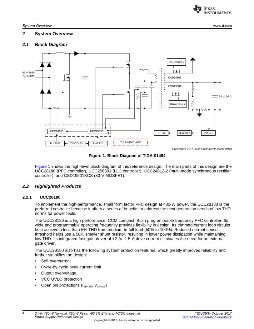
2.1 Block Diagram
Figure 1. Block Diagram of TIDA-01494
Figure 1 shows the high-level block diagram of this reference design. The main parts of this design are theUCC28180 (PFC controller), UCC256301 (LLC controller), UCC24612-2 (multi-mode synchronous rectifiercontroller), and CSD19501KCS (80-V MOSFET).
2.2 Highlighted Products
2.2.1 UCC28180To implement the high-performance, small form factor PFC design at 480-W power, the UCC28180 is thepreferred controller because it offers a series of benefits to address the next generation needs of low THDnorms for power tools.
The UCC28180 is a high-performance, CCM compact, 8-pin programmable frequency PFC controller. Itswide and programmable operating frequency provides flexibility in design. Its trimmed current loop circuitshelp achieve a less than 5% THD from medium-to-full load (50% to 100%). Reduced current sensethreshold helps use a 50% smaller shunt resistor, resulting in lower power dissipation while maintaininglow THD. Its integrated fast gate driver of +2-A/–1.5-A drive current eliminates the need for an externalgate driver.
The UCC28180 also has the following system protection features, which greatly improves reliability andfurther simplifies the design:• Soft overcurrent• Cycle-by-cycle peak current limit• Output overvoltage• VCC UVLO protection• Open pin protections (ISENSE, VSENSE)
www.ti.com System Overview
5TIDUDF3–October 2017Submit Documentation Feedback
Copyright © 2017, Texas Instruments Incorporated
24-V, 480-W Nominal, 720-W Peak, >93.5% Efficient, AC/DC IndustrialPower Supply Reference Design
2.2.2 UCC256301LLC resonant converters are one of the most widely used topologies for implementing medium-to-highpower isolated DC/DC power stages in industrial power supplies. These converters are popular due totheir ability to achieve soft-switching (ZVS turnon) for the high-voltage MOSFET, improving he overallefficiency of the system.
LLC converters in industrial power supplies do face some specific requirements. Some industrial powersupplies need to support an overload (up to 1.5 times the nominal load) for a short period of time. TheLLC converter must not enter the capacitive (ZCS) region during the overload operation; otherwise, it canbe catastrophic. With its ZCS avoidance feature, the UCC256301 can ensure that the system does notenter the ZCS region under all operating conditions, keeping the system safe. Apart from the overload(also known as power boost) functionality, industrial power supplies typically need a tunable output voltagewith a wide range. For example, in a 24-V nominal output system, the output voltage can range from 22 to28 V. The UCC256301 provides a wide operating frequency range from 35 kHz to 1 MHz to make it easierto design wide output voltage range using an LLC converter.
The UCC256301 with its unique hybrid hysteretic control provides excellent line and load transientresponse, minimizing the need for output filter capacitors. Its wide frequency range can be used to reducethe PFC bulk capacitor required to meet the holdup time requirement in the industrial power supplies. Withthe integrated high-voltage gate drive, X-capacitor discharge function, and addition output overvoltageprotection, the UCC256301 reduces the amount of external discreet components required to implement ahigh-efficiency industrial power supply.
2.2.3 UCC24612-2The UCC24612-2 is a multi-mode synchronous rectifier controller for active clamp flyback and LLCapplications. With its 4-A sink and 1-A source capability, the proportional gate drive of the device helps inusing this synchronous rectifier in LLC applications where the system can operate above the resonantfrequency. The adaptive off-time feature adds robustness to the synchronous rectifier by preventing falsetriggering.
2.2.4 CSD19501KCSThe CSD19501KCS is an 80-V NexFET™ with 5.5-mΩ resistance and a 38-nC gate charge. In thisreference design, the CSD19501KCS is used as the synchronous FET to lower the losses in the outputstage of the LLC converter.
2.3 System Design TheoryThis reference design provides universal AC mains powered, 480-W nominal output at 24 V and 20 A.This design is able to support a short-time overload of up to 720 W for > 3 seconds. The UCC28180controls a PFC boost front end, while the UCC25630 LLC resonant half-bridge converts the PFC output toan isolated 24 V and 20 A. The total system efficiency is 93.2% with a 230-V AC input and over 91% witha 110-V AC input at full load. In addition, several protections are embedded into this design, whichincludes input undervoltage protection and output short-circuit protection.
Low EMI, high efficiency, a high power factor, and reliable power supply are the main focus of this designfor targeted applications.
INrms max500
I 6.320.94 85 0.99
u u
OUT maxINrms max
IN max
PI
V PF K u u
OUT max500
I 1.28390
OUT maxOUT max
OUT max
PI
V
System Overview www.ti.com
6 TIDUDF3–October 2017Submit Documentation Feedback
Copyright © 2017, Texas Instruments Incorporated
24-V, 480-W Nominal, 720-W Peak, >93.5% Efficient, AC/DC IndustrialPower Supply Reference Design
2.3.1 PFC Regulator Stage DesignFor high power levels such as 500 W, either the single-phase CCM PFC or interleaved CrCM PFC can bepreferred. CCM PFC has certain advantages at these power levels, such as a lower component count,reduced input peak currents, and simpler EMI filter requirements. CrCM PFC requires smaller PFCinductors and can use ultrafast diode for the PFC boost diode. CrCM PFC also have the advantage ofenabling valley switching and ZCS turnon condition for the PFC MOSFET.
In this design, the CCM PFC is used as it enables a fixed frequency PFC implementation with reducedinput peak currents, which helps reduce the cost.
The UCC28180 operates at fixed frequency in CCM mode and requires minimal external components forhigh-wattage PFC pre-regulator implementation. The design process and component selection for thisdesign are illustrated in the following subsections.
2.3.1.1 Design Parameters
Table 2. Design Parameters for PFC Power Stage Design
PARAMETER MIN TYP MAX UNITINPUTVIN Input voltage 85 — 265 VACfLINE Input frequency 47 — 63 HzOUTPUTVOUT Output voltage — 391 VDCPOUT(nom) Output power — — 500 WPOUT(max) Output power — — 750 W— Line regulation — — 5 %— Load regulation — — 5 %PF Targeted power factor — 0.99 — —η Targeted efficiency — 97.5 — %fSW Mean switching frequency — 70 — kHz
2.3.1.2 Current CalculationsThe input fuse, bridge rectifier, and input capacitor are selected based upon the input current calculations.First, determine the maximum average output current, IOUT(max):
(1)
The maximum input RMS line current, IINrms(max), is calculated using the parameters from Table 2 and theefficiency and power factor initial assumptions:
(2)
2.3.1.3 Boost InductorTo dimension the boost inductor, first calculate the maximum allowed ripple current. The maximum ripplecurrent is observed at the lowest input voltage and maximum load. Assuming a maximum 25% ripple inthe inductor current gives a ripple current:
DSrms500 16 120
I 2 5.05120 3 390
§ ·u u ¨ ¸
S u© ¹
OUT nom INrmsDSrms
OUT maxINrms min
P 16 V 2I 2
3 V2 V
u u u
u S uu
OUT min 2 2
2 500 20 msC 294 F
390 290
u ut P
HoldupOUT OUT(nom) 2 2
OUT max OUT max
TC 2 P
V Vt u u
OUT (max)L max
INrms min
P RIPPLEI 2 1 11.3
V 2
§ · '§ ·¨ ¸ u u ¨ ¸¨ ¸ © ¹© ¹
Boost390 0.691 1 0.691
L 392 H950000 2.23
u u t t P
u
maxBoost OUT(max) (max)
SW RIPPLE max
1 DUTYL V DUTY
f I
t u u
u
(max)390 (1.414 85)
DUTY 0.691390
u
OUT (max) INrms (min)(max)
OUT(max)
V V 2DUTY
V
u
INripple maxI 0.25 2 6.32 2.23 u u
INrms(max)INripple maxI RIPPLE I ' u
www.ti.com System Overview
7TIDUDF3–October 2017Submit Documentation Feedback
Copyright © 2017, Texas Instruments Incorporated
24-V, 480-W Nominal, 720-W Peak, >93.5% Efficient, AC/DC IndustrialPower Supply Reference Design
(3)
The duty cycle, DUTY(max), at the peak of the minimum input voltage can be calculated as:
(4)
The minimum value of the boost inductor is calculated based upon the acceptable ripple current,IINripple(max) , at a worst case duty cycle of 0.691:
(5)
The actual value of the boost inductor used is 420 µH.
The required saturation current for the boost inductor is calculated using Equation 6 for the minimum inputvoltage and short-time maximum overload conditions.
(6)
2.3.1.4 Output CapacitorThe output capacitor, COUT, is sized to meet the holdup requirements of the converter. The holdup timerequired by this design, THoldup, is 20 ms. During this time, the minimum voltage that the PFC output canreach at full load is designed to be VOUT(min) = 290 V. Substituting the known values in Equation 7, theminimum COUT is:
(7)
The capacitor of 330 µF is selected for use in this reference design.
2.3.1.5 Switching ElementThe drain-to-source RMS current, IDSrms, through the PFC MOSFET is calculated as:
(8)
Select a MOSFET with a low figure of merit for this application. The key specifications that are importantfor this topology are:• Low RDSon, for reducing the conduction losses in the MOSFET• Low QG, for fast turnon and turnoff, both of which are hard switched in this topology• Low output capacitance, to reduce COSS related losses
SENSE0.259 V
R 0.02 R4111.3 A 1.1
: u
SOC(min)SENSE
L max
VR
I 1.1
u
System Overview www.ti.com
8 TIDUDF3–October 2017Submit Documentation Feedback
Copyright © 2017, Texas Instruments Incorporated
24-V, 480-W Nominal, 720-W Peak, >93.5% Efficient, AC/DC IndustrialPower Supply Reference Design
2.3.1.6 Boost DiodeThe output diode must have a blocking voltage that exceeds the output overvoltage of the converter andaverage current same as IOUT(max). In CCM PFC topology, the boost diode undergoes hard turnoff andhence suffers from reverse recovery losses.
One way of reducing the reverse recovery loss is by using a silicon-carbide diode. In this design, theTRS6E65F diode is used.
2.3.1.7 Sense ResistorTo accommodate the gain of the nonlinear power limit, the sense resistor, RSENSE, is sized such that ittriggers the soft overcurrent at 10% higher than the maximum peak inductor current using the minimumsoft overcurrent threshold of the ISENSE pin, VSOC, of ISENSE equal to 0.265 V.
(9)
2.3.1.8 Control Loop CompensationThe voltage error amplifier is compensated with a zero, fZERO, at the fPWM_PS pole, and a pole, fPOLE, isplaced at 20 Hz to reject high-frequency noise and roll off the gain amplitude. The overall voltage loopcrossover, fV, is desired to be at 10 Hz. The compensation components of the voltage error amplifier areselected accordingly.
2.3.2 LLC Converter Stage DesignThe DC/DC stage in an industrial AC/DC converter needs to support a wide output voltage range and ahold up time > 20 ms. Combined with the need to meet the short time power boost feature, the LLC-basedDC/DC stage needs to be designed with sufficient gain and proper operating point to maximize efficiency.
Because this DC/DC stage supports a nominal output power of 480 W and a peak output power of 720 W,designing the DC/DC stage for 720-W operation does not give an optimum performance at 480 W. Whiledesigning for 480 W, take care in dimensioning the resonant tank components such that the system doesnot enter into the capacitive region of operation at 720 W.
The hybrid hysteretic mode control and ZCS avoidance of the UCC256301 helps in developing a robustLLC power stage for use in these applications.
Table 3. Design Parameters for LLC Power Stage Design
PARAMETER MIN TYP MAX UNITINPUTVINDC Input voltage 300 397 410 VDCOUTPUTVOUT Output voltage — 24 — VDCPLIMIT Output power limit — — 720 WPOUT Max output power — 480 — WfSW(nom) Nominal switching frequency — 80 — kHz— Line regulation — 1 — %— Load regulation — 1 — %η Targeted efficiency — 0.97 — —
g(max)
28 V300 V
M 7.32 1.3662
§ ·¨ ¸¨ ¸ u ¨ ¸¨ ¸© ¹
0 max
DCIN ming(max)
V
VM n
2
§ ·¨ ¸¨ ¸
u ¨ ¸¨ ¸¨ ¸¨ ¸© ¹
g(min)
22 V410 V
M 7.32 0.7662
§ ·¨ ¸¨ ¸ u ¨ ¸¨ ¸© ¹
0 min
g(min)
V
VDCIN maxM n
2
§ ·¨ ¸¨ ¸
u ¨ ¸¨ ¸¨ ¸© ¹
DCIN nom
g0
V
2n M 7.32V
§ ·¨ ¸¨ ¸ u ¨ ¸¨ ¸© ¹
DCIN nom
g0
V
2n MV
u
www.ti.com System Overview
9TIDUDF3–October 2017Submit Documentation Feedback
Copyright © 2017, Texas Instruments Incorporated
24-V, 480-W Nominal, 720-W Peak, >93.5% Efficient, AC/DC IndustrialPower Supply Reference Design
2.3.2.1 Determine Mg (Voltage Gain)The transformer turns ratio is determined by Equation 10.
(10)
Where Mg is the voltage gain (Mg = 0.9).
From these specifications, the nominal values for input voltage and output voltage are 390 V and 24 V,respectively. As a result, the turns ratio can be calculated as:
(11)
2.3.2.1.1 Determine Mg(min) and Mg(max)
Mg(min) and Mg(max) can be determined by using Equation 12 and Equation 13, respectively:
(12)
(13)
The dimensioned Mg(max) is increased to 1.1 times the required value to handle the power boostfunctionality = Mg(max) = 1.1 × 1.366 ≈ 1.5.
Frequency in KHz
Gai
n
0 50 100 150 200 250 300 350 4000
0.2
0.4
0.6
0.8
1
1.2
1.4
1.6
D005
28 V, 480 W24 V, 480 W24 V, 720 W
r
r r
1F 75.75 kHz
2 L C
u S u
2
e max V 2
8 7.7 28R 78.31
17.2u § ·
u :¨ ¸© ¹S
2
e _ pk 2
8 7.7 24R 38.48
20u § ·
u :¨ ¸© ¹S
2 0 nome _pk 2
0 _pk
V8 nR
I
§ ·u¨ ¸ u¨ ¸S © ¹
2
e nom 2
8 7.7 24R 57.7
20u § ·
u :¨ ¸© ¹S
2 0 nome 2
0 nom
V8 nR
I
§ ·u ¨ ¸ u¨ ¸S © ¹
System Overview www.ti.com
10 TIDUDF3–October 2017Submit Documentation Feedback
Copyright © 2017, Texas Instruments Incorporated
24-V, 480-W Nominal, 720-W Peak, >93.5% Efficient, AC/DC IndustrialPower Supply Reference Design
2.3.2.2 Determine Equivalent Load Resistance (Re) of Resonant NetworkThe equivalent load resistance at nominal and peak load under nominal output voltage and peak outputvoltage are derived in this section.
(14)
Under peak load conditions of 30 A at a 24-V output, the equivalent load resistance is given byEquation 15:
(15)
Similarly, the equivalent load resistance at the maximum output voltage is VO_pk= 28 V.
(16)
2.3.2.3 Select Lm/Lr Ratio (Ln) and Qe
The second resonance point for the LLC converter is set at close to 75 kHz. By choosing a value ofLr = 47 µH and Cr = 94 nF, calculate the value of the resonant frequency to be using Equation 17:
(17)
The magnetizing inductance to resonant inductance ratio is chosen as 6 to develop sufficient gain whileminimizing the magnetizing current in the LLC transformer. By using an integrated magnetics approach,the Lr is realized as the leakage inductor of the main LLC transformer.
The Q curves for this design at different corner conditions are depicted in Figure 2. The corner conditionsoperate at a 28-V output with 480-W output power and at 24-V output with 720-W peak power. The Qcurve for the 24-V output and 480-W output power is also plotted for reference.
Figure 2. Q Curves at Various Normal and Boundary Operating Conditions
sec_ rmsI 15.7
DS max_ sec OUT (max)V 1.2 2 V 1.2 2 28 67.2 u u u
DS INDC maxV 1.2 V 1.2 410 492 V 500 u u o
sec_ rms secI I 15.74S
u
sec_ avgI 10
secI 20
2 2rI 2.883 2.208 3.63
2 2r m priI I I
m2 2 7.7 28
I 2.2022 50 kHz 280 H
§ · § ·u u ¨ ¸ ¨ ¸¨ ¸S u S u u P© ¹© ¹
pri20
I 1.11 2.8837.7
§ · u ¨ ¸
© ¹
Opri
II
n2 2
S § · u ¨ ¸
© ¹
www.ti.com System Overview
11TIDUDF3–October 2017Submit Documentation Feedback
Copyright © 2017, Texas Instruments Incorporated
24-V, 480-W Nominal, 720-W Peak, >93.5% Efficient, AC/DC IndustrialPower Supply Reference Design
2.3.2.4 Determine Primary-Side CurrentsThe primary-side RMS load current (IPRI) at full load is determined from Equation 18:
(18)
The RMS magnetizing current (IM) at fSW(min) = 50 kHz is determined from Equation 19:
(19)
The resonant circuit’s current (Ir) is determined from Equation 20:
(20)
This is also the transformer’s primary winding current at fSW(min).
2.3.2.5 Determine Secondary-Side CurrentsThe secondary-side RMS currents can be calculated from the average load current:
(21)
Assuming the LLC power stage is operating at close to its second resonant frequency, the average currentthrough each rectifier in the secondary-side push-pull output is given as:
(22)
The corresponding half-wave RMS current is:
(23)
2.3.2.6 Select Primary Side MOSFETsEach MOSFET sees the input voltage as its maximum applied voltage:
(24)
For the LLC power stage to work in ZVS, the turnon losses can be neglected. Choose the MOSFET basedon RDS_ON and COSS. Optimizing COSS helps in minimizing the dead time required for achieving ZVS, therebyminimizing duty cycle loss.
For this design, the IPP60R190P6 MOSFET is used. The UCC256301’s adaptive dead-time optimizationfeature helps in maximizing the duty cycle, which improves efficiency.
2.3.2.7 Select Secondary-Side MOSFETsThe diode rectifier voltage rating is determined as:
(25)
The MOSFET’s current rating is determined as:
(26)
TI’s 80-V NexFET CSD19501KCS with its low RDS_ON (< 5.5 mΩ) and Qg (< 38 nC) is used in thisreference design. The very low RDSon of the TI NexFET helps in reducing the overall loss in thesynchronous rectifier.
BWUPPER21 V 4 V
R R17 R12 42.54 V
u
BWLOWERR R12 10
9r
ISNS ISNS 12ISNS
C 94 10R R3 K 0.257 161
C 150 10
u u u
u
ISNSC C39 150 p
ISNSFullload
ISNSOUT(max)
Bulk
V 0.5K 0.257
P 11 757390V
§ · § ·§ · uu ¨ ¸¨ ¸ ¨ ¸ © ¹K © ¹© ¹
ISNSFullloadOCP3 0.6
V 0.51.2 1.2
SS25 A
C C31 400 ms 1.5 F7 VP
u P
System Overview www.ti.com
12 TIDUDF3–October 2017Submit Documentation Feedback
Copyright © 2017, Texas Instruments Incorporated
24-V, 480-W Nominal, 720-W Peak, >93.5% Efficient, AC/DC IndustrialPower Supply Reference Design
2.3.3 Components for UCC256301 ControllerThis section explains the selection of certain components for the LLC power stage controlled by theUCC256301.
2.3.3.1 Soft StartThe UCC256301 is configured to give a maximum of a 400-ms soft start period. During startup, the soft-start capacitor is charged using the 25-µA current source internally. The UCC256301 exits soft start whenthe closed loop control takes over or when the voltage on the soft-start capacitor reaches 7 V. The valueof the soft-start capacitor is selected using Equation 27.
(27)
2.3.3.2 Current Sense CircuitThe overcurrent limit OCP3 is set to trigger at 1.2 times the peak overload capability of the system.
(28)
The current sense ratio is then calculated as:
(29)
Select the current sense capacitor using:
(30)
As a result:
(31)
The R3 is selected as 162 Ω.
2.3.3.3 Overvoltage Protection (BW Pin)The BW pin senses the output voltage through the bias winding mounted on the LLC transformer. This pincan be used to provide an additional overvoltage protection in the system. In this reference design, thebias winding has 0.6 times the turns of the secondary winding, and the overvoltage protection is set at35 V. At this point, the bias winding voltage is at 21 V. Now the BW pin potential divider is set in such away that it sees 4 V at a 35-V output.
Use Equation 32 to select:(32)
As a result:
(33)
2.3.4 Bias Power SupplyThe TIDA-01503 reference design, a 20-W auxiliary power supply based on the UCC28704, is used in thisreference design to provide the bias power to the PFC, LLC, SR, and other logic circuits on the board. Theconverter is powered from the output of the PFC pre-regulator stage and must be able to start up prior tothe PFC stage being operational. For this reason, the circuit is designed to operate over a wide inputvoltage, 100- to 450-V DC. The flyback transformer has three output windings, which are isolated toeach other.
www.ti.com Hardware, Testing Requirements, and Test Results
13TIDUDF3–October 2017Submit Documentation Feedback
Copyright © 2017, Texas Instruments Incorporated
24-V, 480-W Nominal, 720-W Peak, >93.5% Efficient, AC/DC IndustrialPower Supply Reference Design
3 Hardware, Testing Requirements, and Test Results
3.1 Required Hardware
3.1.1 Test ConditionsFor input conditions:• VIN: 85- to 265-V AC• IIN: Current limit to 8 A
For output conditions:• VOUT: 22 to 28 V• IOUT : 0 to 20 A (nominal), 30-A overload
3.1.2 Equipment Needed• Isolated AC source• Single-phase power analyzer• Digital oscilloscope• Multimeters• Electronic load
3.1.3 Procedure1. Adjust the R77 potentiometer to set for a 24-V output.2. Connect input terminals (connector J3) of the reference board to the AC power source.3. Connect output terminals (connector J2) to electronic load, maintaining correct polarity.4. Set minimum load of about 50 mA.5. Gradually increase the input voltage from 0 V to a turnon voltage of 85-V AC. As the input voltage
crosses 85 V, the PFC section starts working and boost the PFC output to 390-V DC.6. Observe the startup conditions for smooth switching waveforms.7. As the PFC output voltage crosses 310 V, the LLC section starts working and the output voltage is
developed.
POUT (W)
iTH
D
0 50 100 150 200 250 300 350 400 450 5002.5%
5%
7.5%
10%
12.5%
15%
17.5%
20%
22.5%
25%
27.5%
D004
115-V AC230-V AC
POUT (W)
Vol
tage
Reg
ulat
ion
0 50 100 150 200 250 300 350 400 450 500-0.35%
-0.3%
-0.25%
-0.2%
-0.15%
-0.1%
-0.05%
0
0.05%
0.1%
0.15%
0.2%
D002
115-V AC230-V AC
POUT (W)
Effi
cien
cy
0 50 100 150 200 250 300 350 400 450 50078%
80%
82%
84%
86%
88%
90%
92%
94%
96%
D001
115-V AC230-V AC
POUT (W)
Pow
er F
acto
r0 50 100 150 200 250 300 350 400 450 500
0.69
0.72
0.75
0.78
0.81
0.84
0.87
0.9
0.93
0.96
0.99
1.02
D003
115-V AC230-V AC
Hardware, Testing Requirements, and Test Results www.ti.com
14 TIDUDF3–October 2017Submit Documentation Feedback
Copyright © 2017, Texas Instruments Incorporated
24-V, 480-W Nominal, 720-W Peak, >93.5% Efficient, AC/DC IndustrialPower Supply Reference Design
3.2 Testing and Results
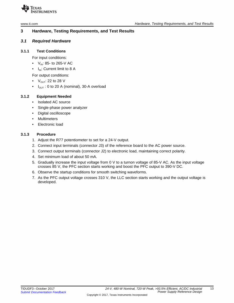
3.2.1 Efficiency and RegulationThis section shows the efficiency, power factor, iTHD, and load regulation results at 115-V and 230-V ACinput conditions.
The following figures show the graphs for efficiency, power factor, iTHD, and load regulation, respectively.
Figure 3. Efficiency Data Figure 4. Power Factor Data
Figure 5. iTHD Data Figure 6. Load Regulation Data
www.ti.com Hardware, Testing Requirements, and Test Results
15TIDUDF3–October 2017Submit Documentation Feedback
Copyright © 2017, Texas Instruments Incorporated
24-V, 480-W Nominal, 720-W Peak, >93.5% Efficient, AC/DC IndustrialPower Supply Reference Design
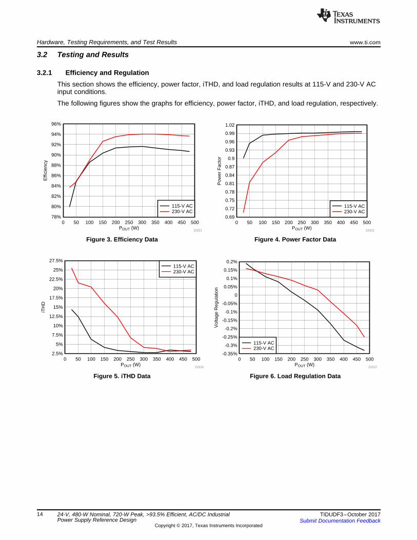
3.2.2 Startup WaveformThe startup waveform showing the 24-V output voltage and the input AC current is shown in Figure 7.Figure 8 shows the same waveform zoomed in.
Figure 7. Startup Waveform at 230-V AC
Figure 8. Startup Waveform at 230-V AC (Zoomed In)
Hardware, Testing Requirements, and Test Results www.ti.com
16 TIDUDF3–October 2017Submit Documentation Feedback
Copyright © 2017, Texas Instruments Incorporated
24-V, 480-W Nominal, 720-W Peak, >93.5% Efficient, AC/DC IndustrialPower Supply Reference Design
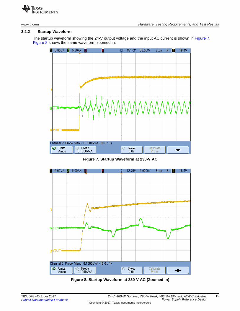
3.2.3 Load Transient ResponseFigure 9 shows the transient response of the system when the 24-V output load varies from 4 to 20 A at aslew rate of 500 mA/µC. The maximum dip is 200 mV on the 24-V output.
Figure 9. Transient Response at 24-V Output
www.ti.com Hardware, Testing Requirements, and Test Results
17TIDUDF3–October 2017Submit Documentation Feedback
Copyright © 2017, Texas Instruments Incorporated
24-V, 480-W Nominal, 720-W Peak, >93.5% Efficient, AC/DC IndustrialPower Supply Reference Design
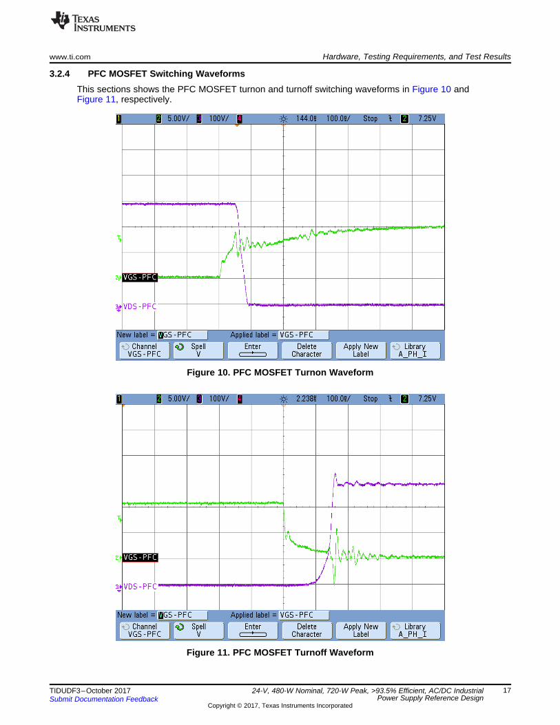
3.2.4 PFC MOSFET Switching WaveformsThis sections shows the PFC MOSFET turnon and turnoff switching waveforms in Figure 10 andFigure 11, respectively.
Figure 10. PFC MOSFET Turnon Waveform
Figure 11. PFC MOSFET Turnoff Waveform
Hardware, Testing Requirements, and Test Results www.ti.com
18 TIDUDF3–October 2017Submit Documentation Feedback
Copyright © 2017, Texas Instruments Incorporated
24-V, 480-W Nominal, 720-W Peak, >93.5% Efficient, AC/DC IndustrialPower Supply Reference Design
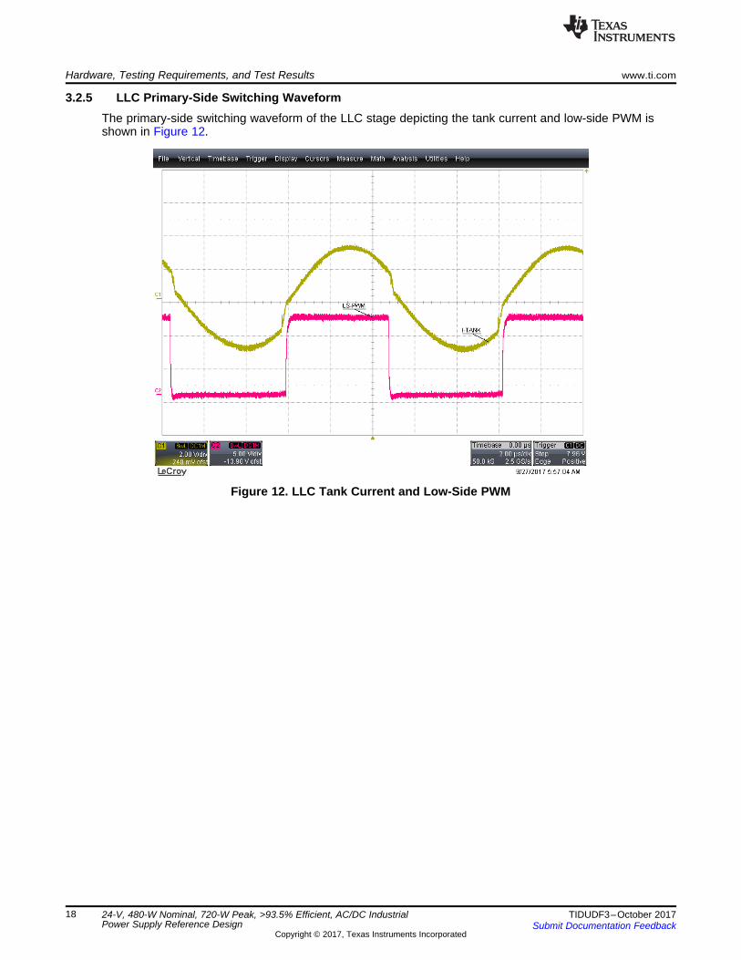
3.2.5 LLC Primary-Side Switching WaveformThe primary-side switching waveform of the LLC stage depicting the tank current and low-side PWM isshown in Figure 12.
Figure 12. LLC Tank Current and Low-Side PWM
www.ti.com Hardware, Testing Requirements, and Test Results
19TIDUDF3–October 2017Submit Documentation Feedback
Copyright © 2017, Texas Instruments Incorporated
24-V, 480-W Nominal, 720-W Peak, >93.5% Efficient, AC/DC IndustrialPower Supply Reference Design
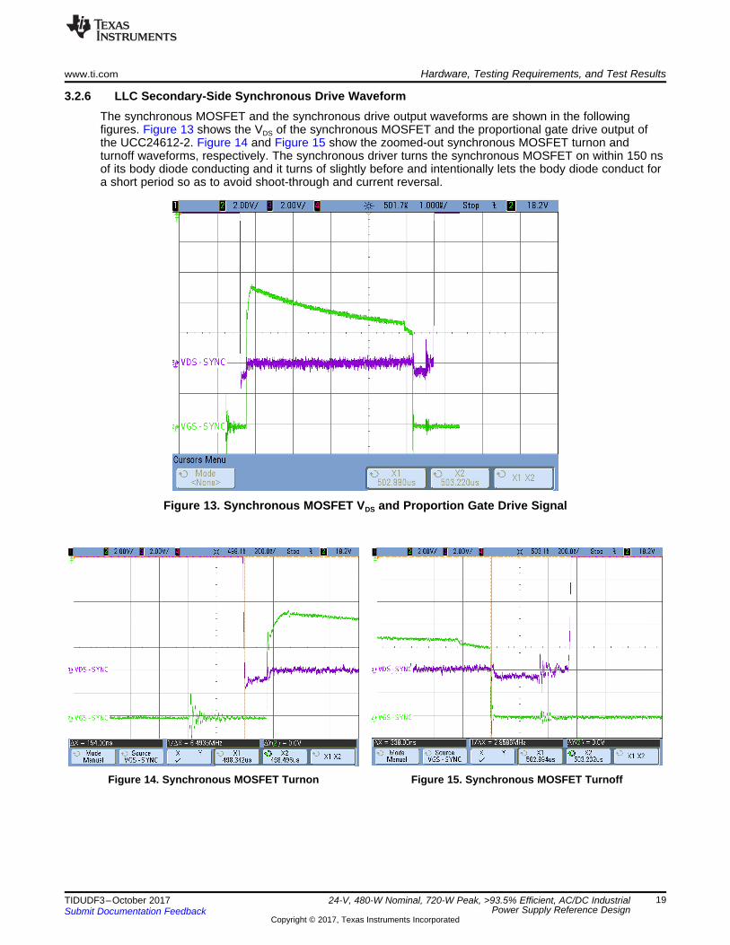
3.2.6 LLC Secondary-Side Synchronous Drive WaveformThe synchronous MOSFET and the synchronous drive output waveforms are shown in the followingfigures. Figure 13 shows the VDS of the synchronous MOSFET and the proportional gate drive output ofthe UCC24612-2. Figure 14 and Figure 15 show the zoomed-out synchronous MOSFET turnon andturnoff waveforms, respectively. The synchronous driver turns the synchronous MOSFET on within 150 nsof its body diode conducting and it turns of slightly before and intentionally lets the body diode conduct fora short period so as to avoid shoot-through and current reversal.
Figure 13. Synchronous MOSFET VDS and Proportion Gate Drive Signal
Figure 14. Synchronous MOSFET Turnon Figure 15. Synchronous MOSFET Turnoff
Hardware, Testing Requirements, and Test Results www.ti.com
20 TIDUDF3–October 2017Submit Documentation Feedback
Copyright © 2017, Texas Instruments Incorporated
24-V, 480-W Nominal, 720-W Peak, >93.5% Efficient, AC/DC IndustrialPower Supply Reference Design
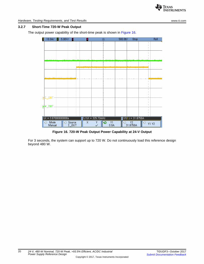
3.2.7 Short-Time 720-W Peak OutputThe output power capability of the short-time peak is shown in Figure 16.
Figure 16. 720-W Peak Output Power Capability at 24-V Output
For 3 seconds, the system can support up to 720 W. Do not continuously load this reference designbeyond 480 W.
www.ti.com Hardware, Testing Requirements, and Test Results
21TIDUDF3–October 2017Submit Documentation Feedback
Copyright © 2017, Texas Instruments Incorporated
24-V, 480-W Nominal, 720-W Peak, >93.5% Efficient, AC/DC IndustrialPower Supply Reference Design
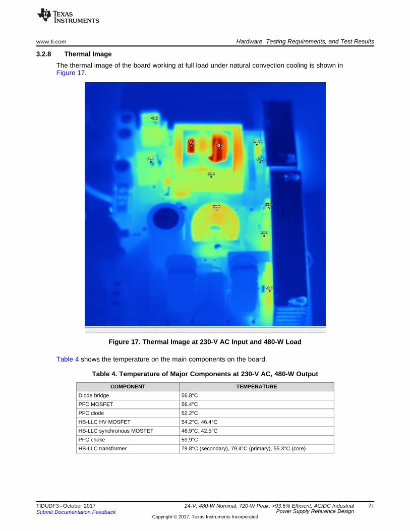
3.2.8 Thermal ImageThe thermal image of the board working at full load under natural convection cooling is shown inFigure 17.
Figure 17. Thermal Image at 230-V AC Input and 480-W Load
Table 4 shows the temperature on the main components on the board.
Table 4. Temperature of Major Components at 230-V AC, 480-W Output
COMPONENT TEMPERATUREDiode bridge 56.8°CPFC MOSFET 56.4°CPFC diode 52.2°CHB-LLC HV MOSFET 54.2°C, 46.4°CHB-LLC synchronous MOSFET 46.9°C, 42.5°CPFC choke 59.9°CHB-LLC transformer 79.8°C (secondary), 79.4°C (primary), 55.3°C (core)
Design Files www.ti.com
22 TIDUDF3–October 2017Submit Documentation Feedback
Copyright © 2017, Texas Instruments Incorporated
24-V, 480-W Nominal, 720-W Peak, >93.5% Efficient, AC/DC IndustrialPower Supply Reference Design
4 Design Files
4.1 SchematicsTo download the schematics, see the design files at TIDA-01494.
4.2 Bill of MaterialsTo download the bill of materials (BOM), see the design files at TIDA-01494.
4.3 PCB Layout Recommendations
4.3.1 Layout PrintsTo download the layer plots, see the design files at TIDA-01494.
4.4 Altium ProjectTo download the Altium project files, see the design files at TIDA-01494.
4.5 Gerber FilesTo download the Gerber files, see the design files at TIDA-01494.
4.6 Assembly DrawingsTo download the assembly drawings, see the design files at TIDA-01494.
5 Software FilesTo download the software files, see the design files at TIDA-01494.
6 Related Documentation
1. Texas Instruments, Designing an LLC Resonant Half-Bridge Power Converter, Power Supply DesignSeminar (SLUP263)
2. Texas Instruments, Feedback Loop Design of an LLC Resonant Power Converter, Application Report(SLUA582)
3. Texas Instruments, UCC256301 Hybrid Hysteretic Mode Wide VIN LLC Resonant Controller EnablingUltra-Low Standby Power, Datasheet (SLUSCU6)
6.1 TrademarksE2E, NexFET are trademarks of Texas Instruments.ENERGY STAR is a registered trademark of U.S. Environmental Protection Agency.All other trademarks are the property of their respective owners.
7 About the AuthorRAMKUMAR S is a systems engineer at Texas Instruments, where he is responsible for developingreference design solutions for the industrial segment. Ramkumar brings his diverse experience in analogand digital power supplies design to this role. Ramkumar earned his master of technology (M.Tech) fromthe Indian Institute of Technology in Delhi.

IMPORTANT NOTICE FOR TI DESIGN INFORMATION AND RESOURCES
Texas Instruments Incorporated (‘TI”) technical, application or other design advice, services or information, including, but not limited to,reference designs and materials relating to evaluation modules, (collectively, “TI Resources”) are intended to assist designers who aredeveloping applications that incorporate TI products; by downloading, accessing or using any particular TI Resource in any way, you(individually or, if you are acting on behalf of a company, your company) agree to use it solely for this purpose and subject to the terms ofthis Notice.TI’s provision of TI Resources does not expand or otherwise alter TI’s applicable published warranties or warranty disclaimers for TIproducts, and no additional obligations or liabilities arise from TI providing such TI Resources. TI reserves the right to make corrections,enhancements, improvements and other changes to its TI Resources.You understand and agree that you remain responsible for using your independent analysis, evaluation and judgment in designing yourapplications and that you have full and exclusive responsibility to assure the safety of your applications and compliance of your applications(and of all TI products used in or for your applications) with all applicable regulations, laws and other applicable requirements. Yourepresent that, with respect to your applications, you have all the necessary expertise to create and implement safeguards that (1)anticipate dangerous consequences of failures, (2) monitor failures and their consequences, and (3) lessen the likelihood of failures thatmight cause harm and take appropriate actions. You agree that prior to using or distributing any applications that include TI products, youwill thoroughly test such applications and the functionality of such TI products as used in such applications. TI has not conducted anytesting other than that specifically described in the published documentation for a particular TI Resource.You are authorized to use, copy and modify any individual TI Resource only in connection with the development of applications that includethe TI product(s) identified in such TI Resource. NO OTHER LICENSE, EXPRESS OR IMPLIED, BY ESTOPPEL OR OTHERWISE TOANY OTHER TI INTELLECTUAL PROPERTY RIGHT, AND NO LICENSE TO ANY TECHNOLOGY OR INTELLECTUAL PROPERTYRIGHT OF TI OR ANY THIRD PARTY IS GRANTED HEREIN, including but not limited to any patent right, copyright, mask work right, orother intellectual property right relating to any combination, machine, or process in which TI products or services are used. Informationregarding or referencing third-party products or services does not constitute a license to use such products or services, or a warranty orendorsement thereof. Use of TI Resources may require a license from a third party under the patents or other intellectual property of thethird party, or a license from TI under the patents or other intellectual property of TI.TI RESOURCES ARE PROVIDED “AS IS” AND WITH ALL FAULTS. TI DISCLAIMS ALL OTHER WARRANTIES ORREPRESENTATIONS, EXPRESS OR IMPLIED, REGARDING TI RESOURCES OR USE THEREOF, INCLUDING BUT NOT LIMITED TOACCURACY OR COMPLETENESS, TITLE, ANY EPIDEMIC FAILURE WARRANTY AND ANY IMPLIED WARRANTIES OFMERCHANTABILITY, FITNESS FOR A PARTICULAR PURPOSE, AND NON-INFRINGEMENT OF ANY THIRD PARTY INTELLECTUALPROPERTY RIGHTS.TI SHALL NOT BE LIABLE FOR AND SHALL NOT DEFEND OR INDEMNIFY YOU AGAINST ANY CLAIM, INCLUDING BUT NOTLIMITED TO ANY INFRINGEMENT CLAIM THAT RELATES TO OR IS BASED ON ANY COMBINATION OF PRODUCTS EVEN IFDESCRIBED IN TI RESOURCES OR OTHERWISE. IN NO EVENT SHALL TI BE LIABLE FOR ANY ACTUAL, DIRECT, SPECIAL,COLLATERAL, INDIRECT, PUNITIVE, INCIDENTAL, CONSEQUENTIAL OR EXEMPLARY DAMAGES IN CONNECTION WITH ORARISING OUT OF TI RESOURCES OR USE THEREOF, AND REGARDLESS OF WHETHER TI HAS BEEN ADVISED OF THEPOSSIBILITY OF SUCH DAMAGES.You agree to fully indemnify TI and its representatives against any damages, costs, losses, and/or liabilities arising out of your non-compliance with the terms and provisions of this Notice.This Notice applies to TI Resources. Additional terms apply to the use and purchase of certain types of materials, TI products and services.These include; without limitation, TI’s standard terms for semiconductor products http://www.ti.com/sc/docs/stdterms.htm), evaluationmodules, and samples (http://www.ti.com/sc/docs/sampterms.htm).
Mailing Address: Texas Instruments, Post Office Box 655303, Dallas, Texas 75265Copyright © 2017, Texas Instruments Incorporated