Embed Size (px)
Citation preview
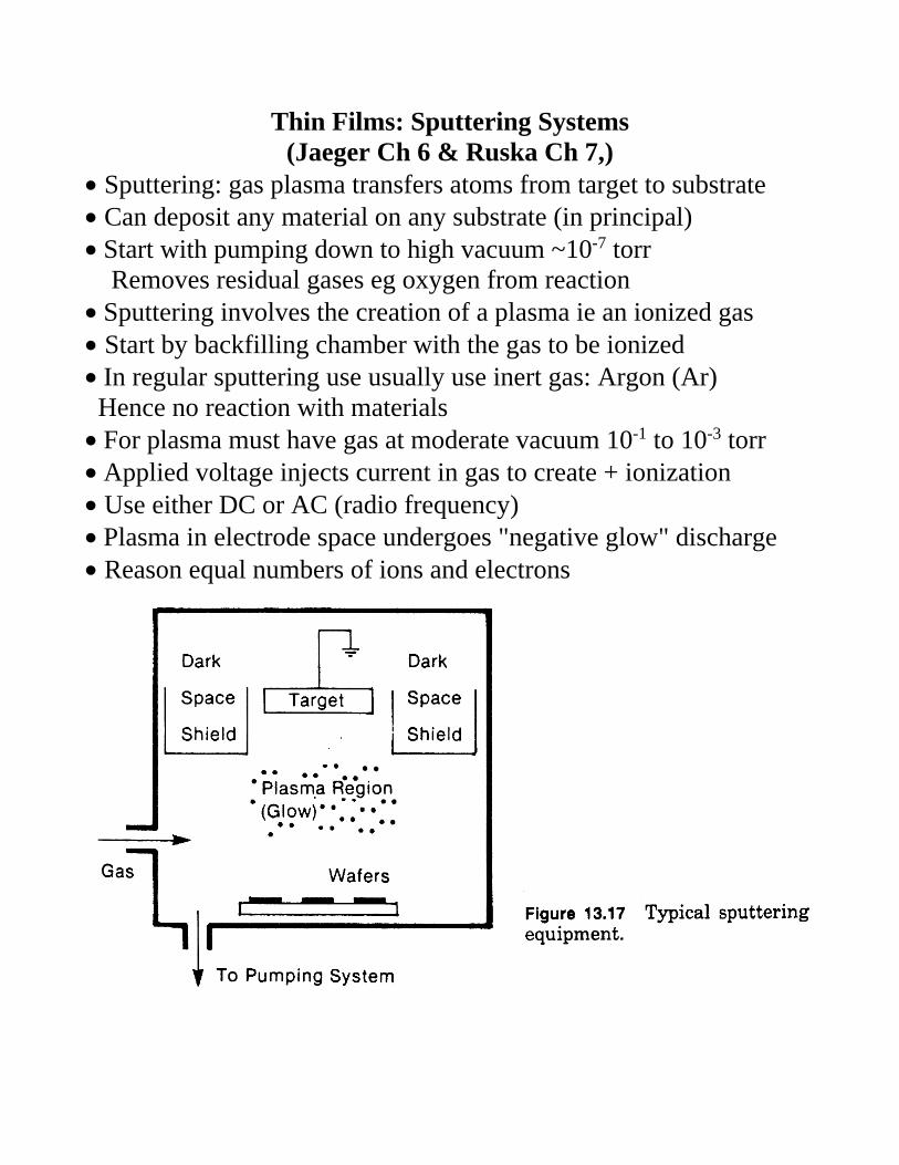
Thin Films: Sputtering Systems (Jaeger Ch 6 & Ruska Ch 7,)
• Sputtering: gas plasma transfers atoms from target to substrate • Can deposit any material on any substrate (in principal) • Start with pumping down to high vacuum ~10-7 torr Removes residual gases eg oxygen from reaction • Sputtering involves the creation of a plasma ie an ionized gas • Start by backfilling chamber with the gas to be ionized • In regular sputtering use usually use inert gas: Argon (Ar) Hence no reaction with materials • For plasma must have gas at moderate vacuum 10-1 to 10-3 torr • Applied voltage injects current in gas to create + ionization • Use either DC or AC (radio frequency) • Plasma in electrode space undergoes "negative glow" discharge • Reason equal numbers of ions and electrons
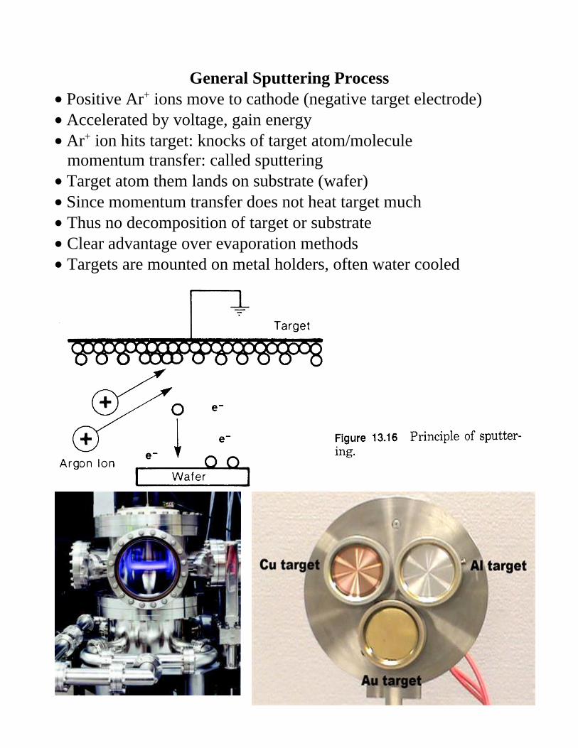
General Sputtering Process • Positive Ar+ ions move to cathode (negative target electrode) • Accelerated by voltage, gain energy • Ar+ ion hits target: knocks of target atom/molecule momentum transfer: called sputtering • Target atom them lands on substrate (wafer) • Since momentum transfer does not heat target much • Thus no decomposition of target or substrate • Clear advantage over evaporation methods • Targets are mounted on metal holders, often water cooled
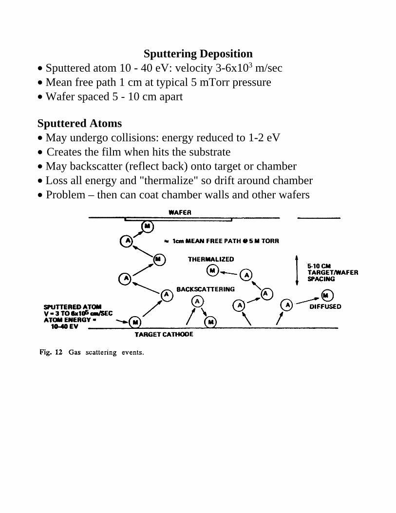
Sputtering Deposition • Sputtered atom 10 - 40 eV: velocity 3-6x10³ m/sec • Mean free path 1 cm at typical 5 mTorr pressure • Wafer spaced 5 - 10 cm apart Sputtered Atoms • May undergo collisions: energy reduced to 1-2 eV • Creates the film when hits the substrate • May backscatter (reflect back) onto target or chamber • Loss all energy and "thermalize" so drift around chamber • Problem – then can coat chamber walls and other wafers
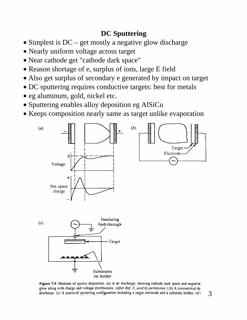
DC Sputtering • Simplest is DC – get mostly a negative glow discharge • Nearly uniform voltage across target • Near cathode get "cathode dark space" • Reason shortage of e, surplus of ions, large E field • Also get surplus of secondary e generated by impact on target • DC sputtering requires conductive targets: best for metals • eg aluminum, gold, nickel etc. • Sputtering enables alloy deposition eg AlSiCu • Keeps composition nearly same as target unlike evaporation
3
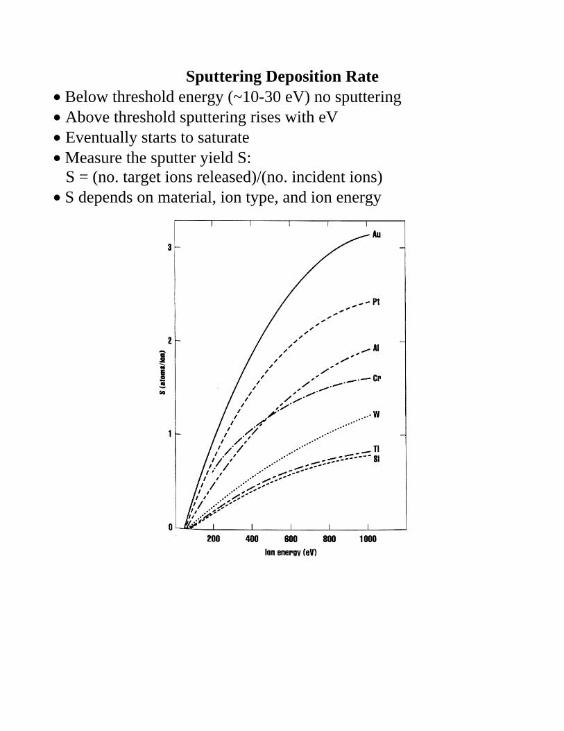
Sputtering Deposition Rate • Below threshold energy (~10-30 eV) no sputtering • Above threshold sputtering rises with eV • Eventually starts to saturate • Measure the sputter yield S: S = (no. target ions released)/(no. incident ions) • S depends on material, ion type, and ion energy
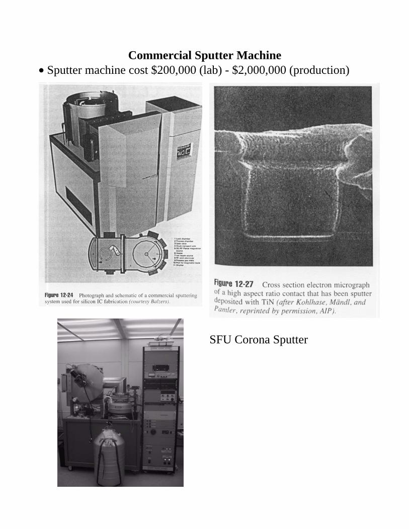
Commercial Sputter Machine • Sputter machine cost $200,000 (lab) - $2,000,000 (production)
SFU Corona Sputter
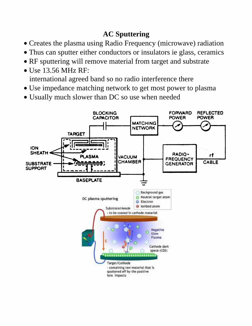
AC Sputtering • Creates the plasma using Radio Frequency (microwave) radiation • Thus can sputter either conductors or insulators ie glass, ceramics • RF sputtering will remove material from target and substrate • Use 13.56 MHz RF: international agreed band so no radio interference there • Use impedance matching network to get most power to plasma • Usually much slower than DC so use when needed
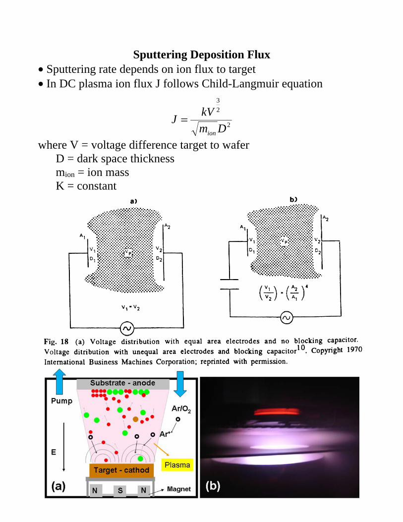
Sputtering Deposition Flux • Sputtering rate depends on ion flux to target • In DC plasma ion flux J follows Child-Langmuir equation
2
2
3
Dm
kVJ
ion
=
where V = voltage difference target to wafer D = dark space thickness mion = ion mass K = constant
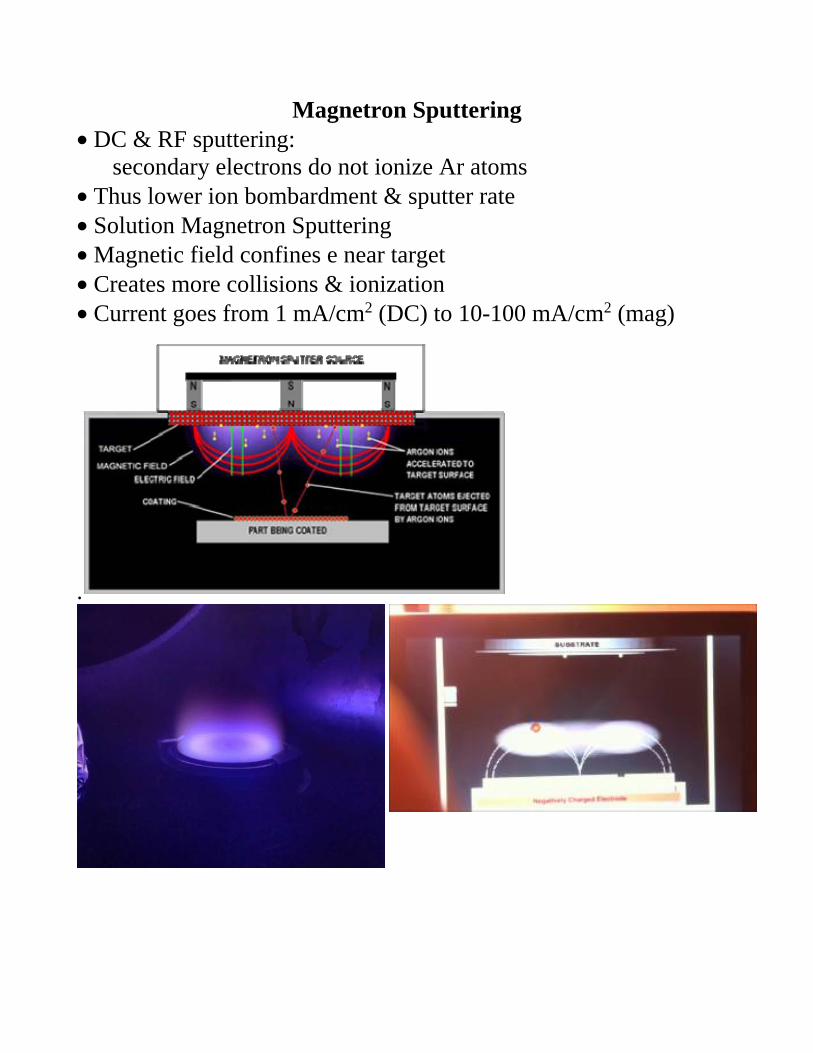
Magnetron Sputtering • DC & RF sputtering: secondary electrons do not ionize Ar atoms • Thus lower ion bombardment & sputter rate • Solution Magnetron Sputtering • Magnetic field confines e near target • Creates more collisions & ionization • Current goes from 1 mA/cm2 (DC) to 10-100 mA/cm2 (mag)
.
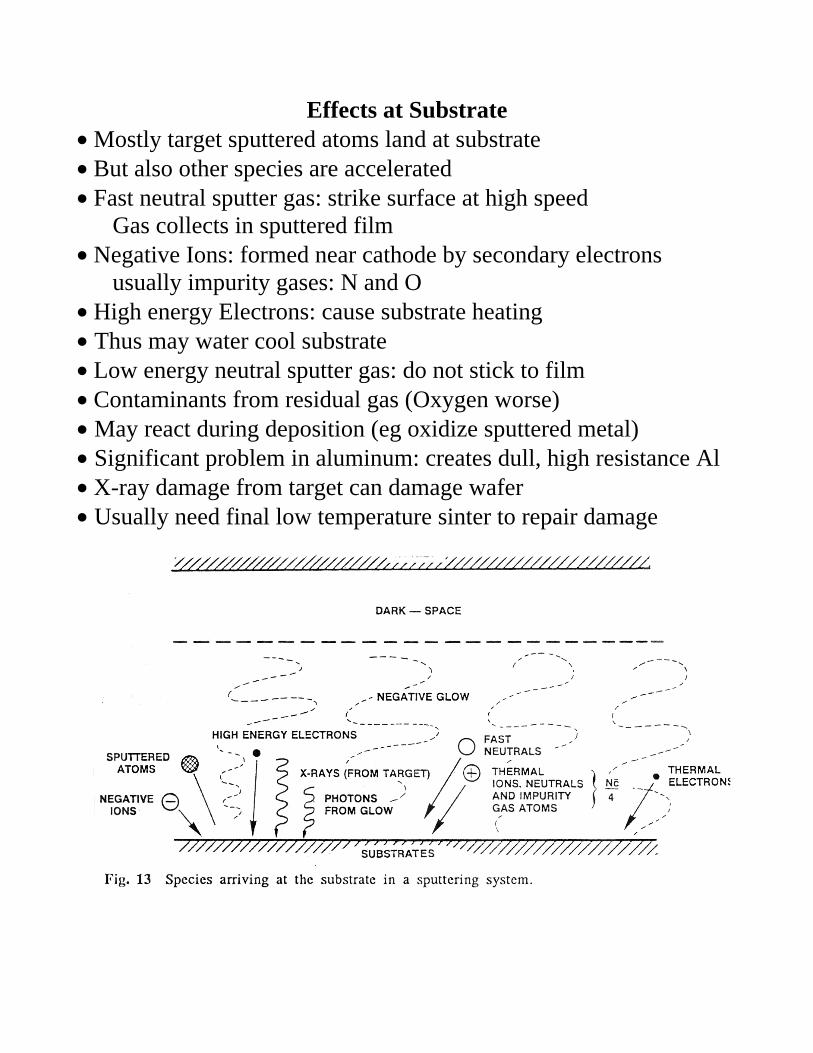
Effects at Substrate • Mostly target sputtered atoms land at substrate • But also other species are accelerated • Fast neutral sputter gas: strike surface at high speed Gas collects in sputtered film • Negative Ions: formed near cathode by secondary electrons usually impurity gases: N and O • High energy Electrons: cause substrate heating • Thus may water cool substrate • Low energy neutral sputter gas: do not stick to film • Contaminants from residual gas (Oxygen worse) • May react during deposition (eg oxidize sputtered metal) • Significant problem in aluminum: creates dull, high resistance Al • X-ray damage from target can damage wafer • Usually need final low temperature sinter to repair damage
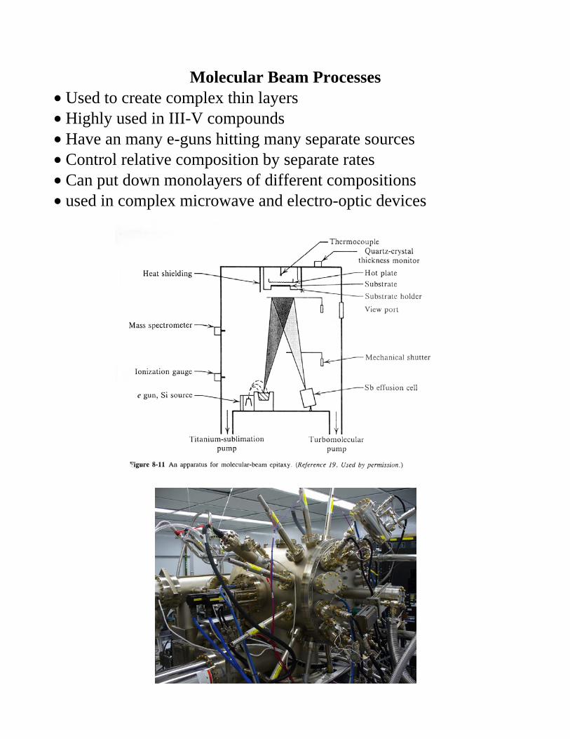
Molecular Beam Processes • Used to create complex thin layers • Highly used in III-V compounds • Have an many e-guns hitting many separate sources • Control relative composition by separate rates • Can put down monolayers of different compositions • used in complex microwave and electro-optic devices
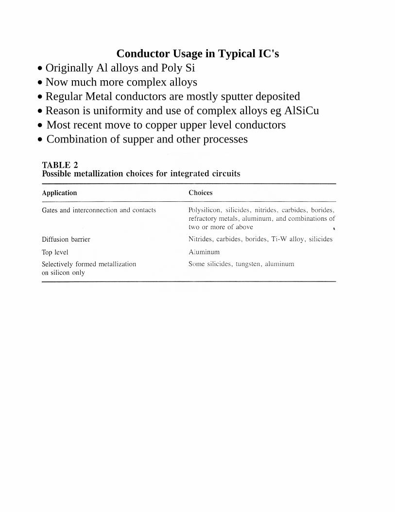
Conductor Usage in Typical IC's • Originally Al alloys and Poly Si • Now much more complex alloys • Regular Metal conductors are mostly sputter deposited • Reason is uniformity and use of complex alloys eg AlSiCu • Most recent move to copper upper level conductors • Combination of supper and other processes
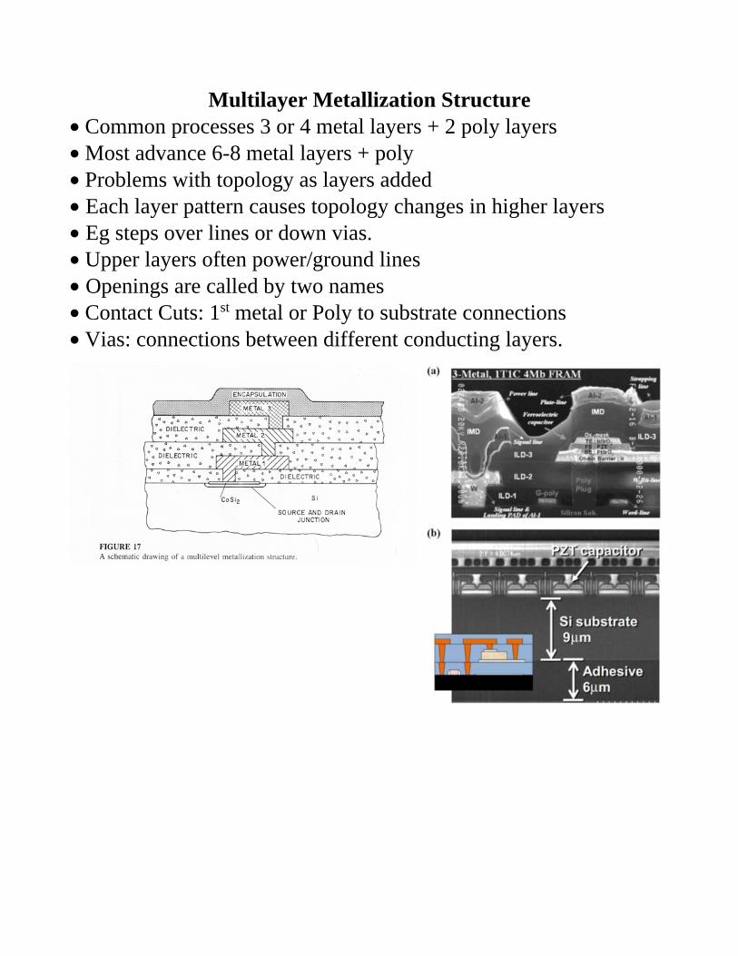
Multilayer Metallization Structure • Common processes 3 or 4 metal layers + 2 poly layers • Most advance 6-8 metal layers + poly • Problems with topology as layers added • Each layer pattern causes topology changes in higher layers • Eg steps over lines or down vias. • Upper layers often power/ground lines • Openings are called by two names • Contact Cuts: 1st metal or Poly to substrate connections • Vias: connections between different conducting layers.
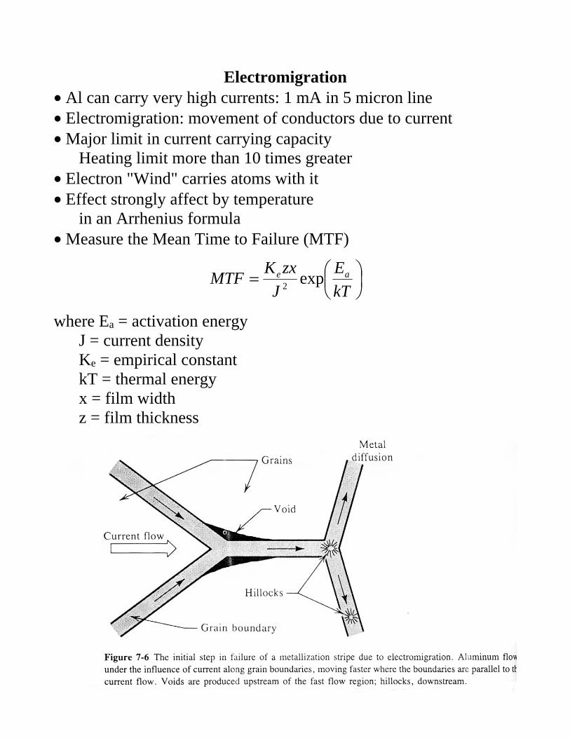
Electromigration • Al can carry very high currents: 1 mA in 5 micron line • Electromigration: movement of conductors due to current • Major limit in current carrying capacity Heating limit more than 10 times greater • Electron "Wind" carries atoms with it • Effect strongly affect by temperature in an Arrhenius formula • Measure the Mean Time to Failure (MTF)
=
kT
E
J
zxKMTF ae exp
2
where Ea = activation energy J = current density Ke = empirical constant kT = thermal energy x = film width z = film thickness
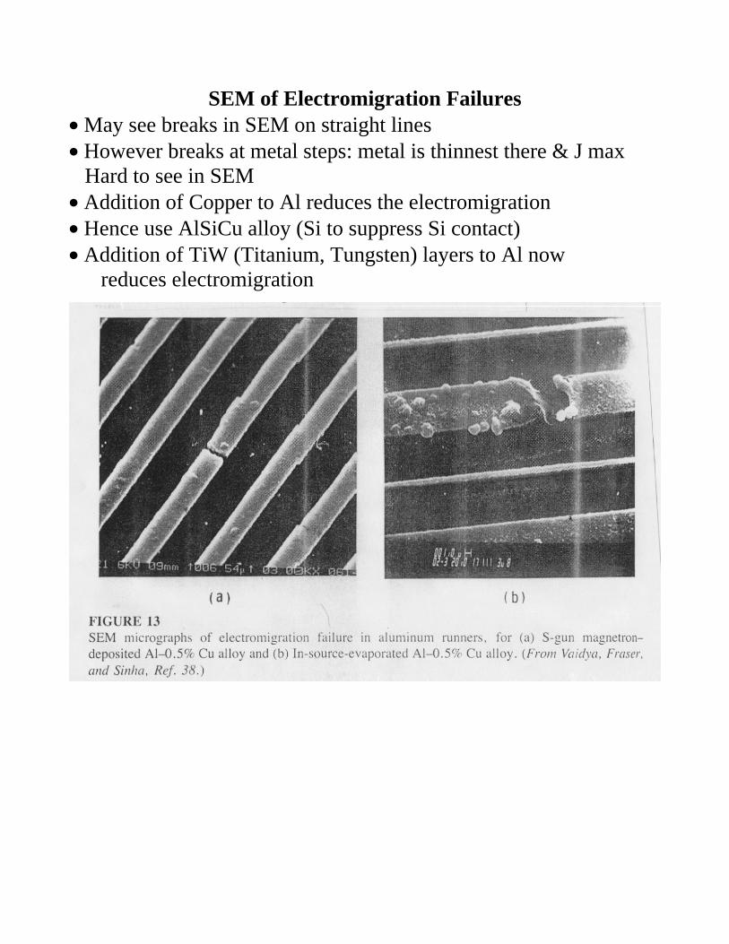
SEM of Electromigration Failures • May see breaks in SEM on straight lines • However breaks at metal steps: metal is thinnest there & J max Hard to see in SEM • Addition of Copper to Al reduces the electromigration • Hence use AlSiCu alloy (Si to suppress Si contact) • Addition of TiW (Titanium, Tungsten) layers to Al now reduces electromigration
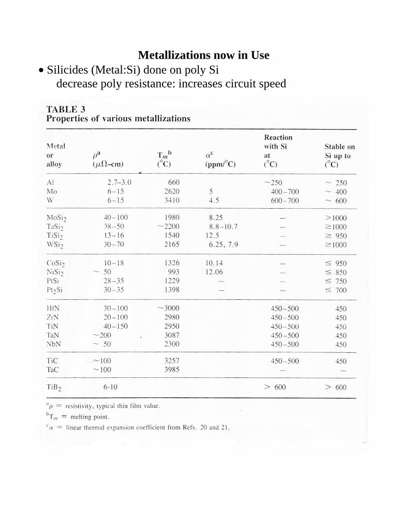
Metallizations now in Use • Silicides (Metal:Si) done on poly Si decrease poly resistance: increases circuit speed
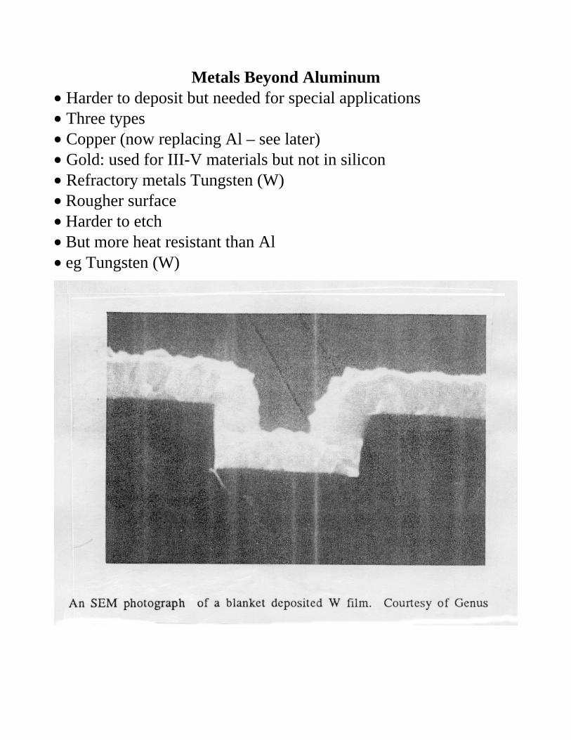
Metals Beyond Aluminum • Harder to deposit but needed for special applications • Three types • Copper (now replacing Al – see later) • Gold: used for III-V materials but not in silicon • Refractory metals Tungsten (W) • Rougher surface • Harder to etch • But more heat resistant than Al • eg Tungsten (W)
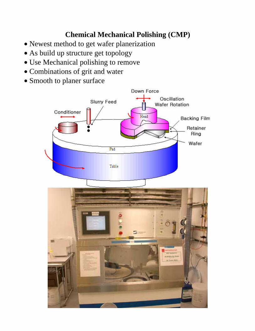
Chemical Mechanical Polishing (CMP) • Newest method to get wafer planerization • As build up structure get topology • Use Mechanical polishing to remove • Combinations of grit and water • Smooth to planer surface
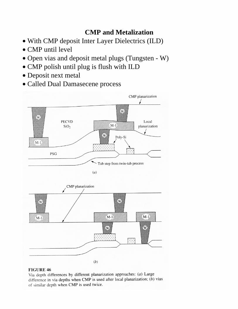
CMP and Metalization • With CMP deposit Inter Layer Dielectrics (ILD) • CMP until level • Open vias and deposit metal plugs (Tungsten - W) • CMP polish until plug is flush with ILD • Deposit next metal • Called Dual Damasecene process
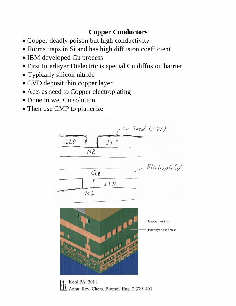
Copper Conductors • Copper deadly poison but high conductivity • Forms traps in Si and has high diffusion coefficient • IBM developed Cu process • First Interlayer Dielectric is special Cu diffusion barrier • Typically silicon nitride • CVD deposit thin copper layer • Acts as seed to Copper electroplating • Done in wet Cu solution • Then use CMP to planerize
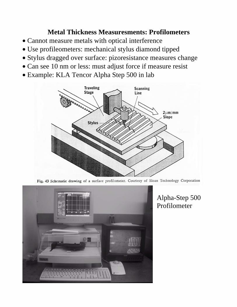
Metal Thickness Measuresments: Profilometers • Cannot measure metals with optical interference • Use profileometers: mechanical stylus diamond tipped • Stylus dragged over surface: pizoresistance measures change • Can see 10 nm or less: must adjust force if measure resist • Example: KLA Tencor Alpha Step 500 in lab
Alpha-Step 500 Profilometer
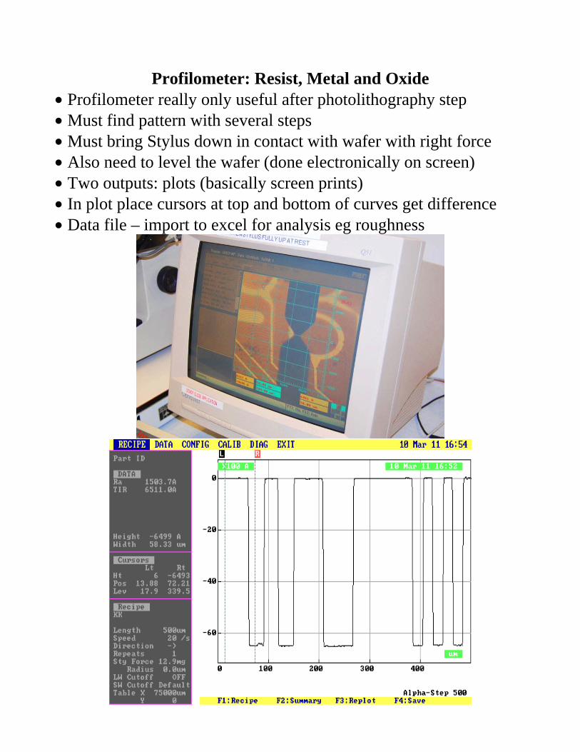
Profilometer: Resist, Metal and Oxide • Profilometer really only useful after photolithography step • Must find pattern with several steps • Must bring Stylus down in contact with wafer with right force • Also need to level the wafer (done electronically on screen) • Two outputs: plots (basically screen prints) • In plot place cursors at top and bottom of curves get difference • Data file – import to excel for analysis eg roughness
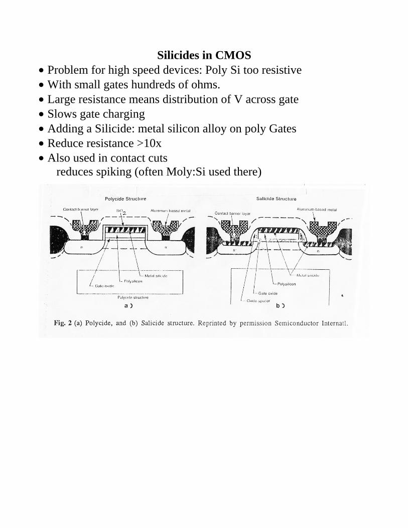
Silicides in CMOS • Problem for high speed devices: Poly Si too resistive • With small gates hundreds of ohms. • Large resistance means distribution of V across gate • Slows gate charging • Adding a Silicide: metal silicon alloy on poly Gates • Reduce resistance >10x • Also used in contact cuts reduces spiking (often Moly:Si used there)
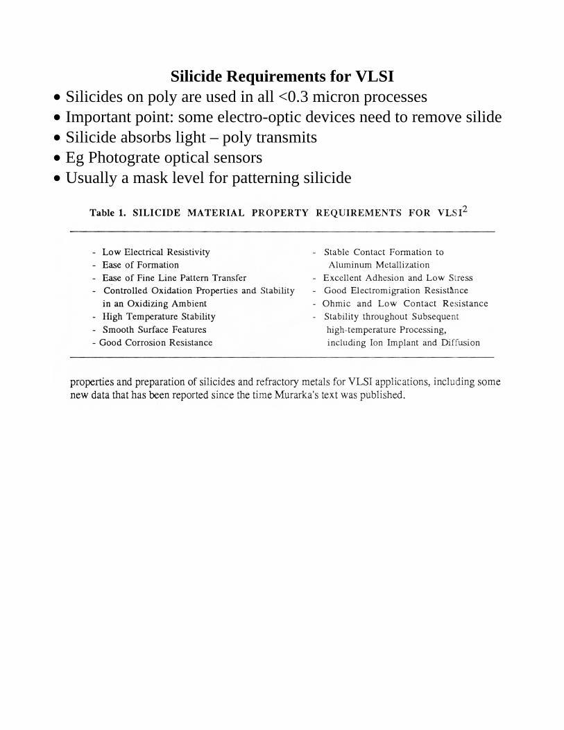
Silicide Requirements for VLSI • Silicides on poly are used in all <0.3 micron processes • Important point: some electro-optic devices need to remove silide • Silicide absorbs light – poly transmits • Eg Photograte optical sensors • Usually a mask level for patterning silicide
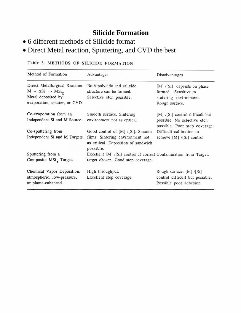
Silicide Formation • 6 different methods of Silicide format • Direct Metal reaction, Sputtering, and CVD the best
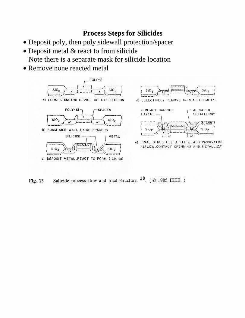
Process Steps for Silicides • Deposit poly, then poly sidewall protection/spacer • Deposit metal & react to from silicide Note there is a separate mask for silicide location • Remove none reacted metal
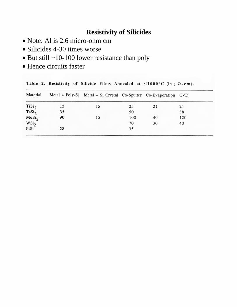
Resistivity of Silicides • Note: Al is 2.6 micro-ohm cm • Silicides 4-30 times worse • But still ~10-100 lower resistance than poly • Hence circuits faster
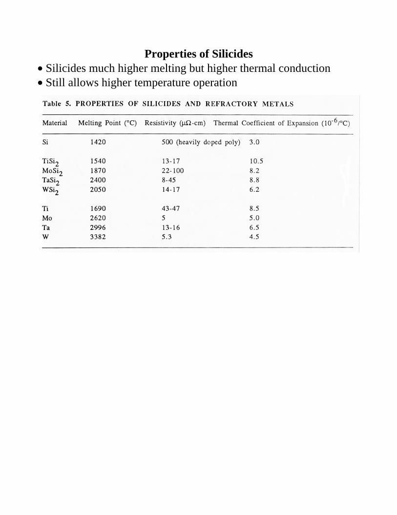
Properties of Silicides • Silicides much higher melting but higher thermal conduction • Still allows higher temperature operation