Embed Size (px)
Citation preview

18
CHAPTER 2
VIENNA RECTIFIER
Abstract— A synchronous logic control based three-phase boost unity power factor rectifier
unit that works as an interface to ensure high energy efficiency by reducing reactive power
consumption and supply current harmonics, as well as to maintain a constant DC-bus
voltage. This chapter discusses the determination of performance characteristics of Vienna
rectifier topology with the synchronous logic based control. Furthermore this enabled the
design and development of a three-phase active rectifier system that was built and tested with
the inputs and output. This chapter also describes the Vienna Rectifier’s power stage and
phase angle control based synchronous logic technique, with particular emphasis on finding
differences between real prototype results and the simulation results. The design and
experimental performance of a three-phase rectifier with a power output of 3 kW is
presented. The real prototype results confirm with the simulation results.
2.1 Introduction
Many high power equipments derive electrical power from three-phase mains, incorporating
an active three-phase PFC front end can contribute significantly in improving overall power
factor, reducing line pollution, lowering component stresses and reducing component size
(e.g. the filter capacitor). Stationary operational behavior of three-phase/switch/level PWM
rectifier was analyzed [24] for asymmetrical loading of the output voltages. Maximum
admissible load of the neutral point that is capacitive output voltage center point was
calculated.
This topology mentioned known as the VIENNA rectifier and the three-level power structure
19
results in a low blocking voltage stress on the power semiconductors and a small input
inductor value and size. Therefore, Vienna is an ideal choice for the implementation of a
medium power, unity power factor rectifier that also has a high power density.
Three-phase AC to DC diode rectifier with three low-power and low frequency, four-
quadrant switches, with high power factor was presented in [9]. The main features were low
cost, small size, high efficiency and simplicity. The high power factor was achieved with
three active bidirectional switches rated at a small fraction of the total power, and gated at the
line frequency.
Application of power module (IXYS VUM25-E) realizing bridge legs of a three-
phase/switch/level VIENNA rectifier system with low effects on the mains were discussed in
[25]. This can be a step in the modularization direction. The switching losses and on-state
losses of a bridge leg of a rectifier were analyzed to determine the maximum output power.
Three-phase diode bridge and DC/DC boost converter combination yielded a three
phase/switch/level PWM rectifier [26]. Sinusoidal mains current, controlled output voltage
and low blocking voltage stress on the power switches were characterized. Due to high
current rate of rise when the phase transistors are turned on the single phase diode bridges in
center point legs cannot be realized as mains rectifier. Diodes with short forward recovery
time have to be applied to avoid high turn-on losses.
Detailed operation and control of VIENNA rectifiers have been reported by Kolar etal. [22-
26], Mehl etal. [8] and Qiao etal. [37]. Major drawback of the VIENNA topology compared

20
to the full bridge is that it does not allow bi-directional power flow.
The Vienna topology can be implemented with either three switches or six switches. A six
switch Vienna Rectifier (see Fig. 1) was selected to lower conduction losses since the phase
current flows through only one diode in each phase during the switch conduction and
guaranteed to clamp the switch voltage to only half the output voltage.
New controller was proposed with one or two integrators and a reset along with several
comparators and flip/flops in [37]. Control was implemented by sensing either inductor
currents or switching currents without multipliers or input voltage sensors.
Three-phase active rectifier (converter) system was built and tested with the inputs and
output. The results confirmed the theoretical analysis. The rectifier was designed to operate
over a wide line-to-line input voltage range of 160 to 520 Vrms, while delivering a nominal
output power output of 3 kW. For an output power of 3 kW and voltage of 900 Vdc, the input
phase current was about 4.5 Arms.
Design and prototype results of a new forced air cooled, three-phase, six-switch, 3 kW output
power, PWM Vienna Rectifier is presented here. The complete chapter is organized as
follows: Section 2.2 explains design strategy of Vienna Converter. Section 2.3 discusses
details of the converter analysis. The system simulation presented in Section 2.4. The
simulation results, comparison and discussion are presented in Section 2.5. Details on the
experimental performance, such as the input currents and respective harmonics, output
voltage, load current, mid-point voltage and input voltages are given in Section 2.6. The
21
overall converter system performances with the synchronous logic control implementation
are summarized in Section 2.7.
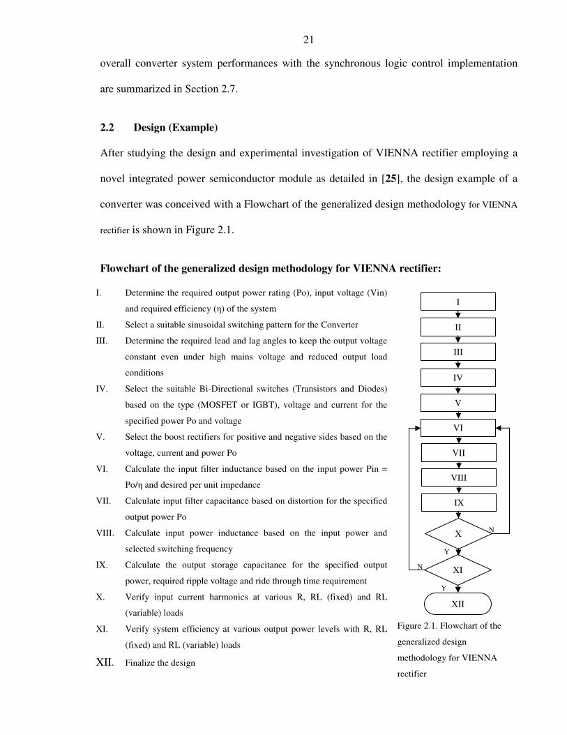
2.2 Design (Example)
After studying the design and experimental investigation of VIENNA rectifier employing a
novel integrated power semiconductor module as detailed in [25], the design example of a
converter was conceived with a Flowchart of the generalized design methodology for VIENNA
rectifier is shown in Figure 2.1.
Flowchart of the generalized design methodology for VIENNA rectifier:
I. Determine the required output power rating (Po), input voltage (Vin)
and required efficiency (η) of the system
II. Select a suitable sinusoidal switching pattern for the Converter
III. Determine the required lead and lag angles to keep the output voltage
constant even under high mains voltage and reduced output load
conditions
IV. Select the suitable Bi-Directional switches (Transistors and Diodes)
based on the type (MOSFET or IGBT), voltage and current for the
specified power Po and voltage
V. Select the boost rectifiers for positive and negative sides based on the
voltage, current and power Po
VI. Calculate the input filter inductance based on the input power Pin =
Po/η and desired per unit impedance
VII. Calculate input filter capacitance based on distortion for the specified
output power Po
VIII. Calculate input power inductance based on the input power and
selected switching frequency
IX. Calculate the output storage capacitance for the specified output
power, required ripple voltage and ride through time requirement
X. Verify input current harmonics at various R, RL (fixed) and RL
(variable) loads
XI. Verify system efficiency at various output power levels with R, RL
(fixed) and RL (variable) loads
XII. Finalize the design
Figure 2.1. Flowchart of the
generalized design
methodology for VIENNA
rectifier
N
Y
Y
N
I
III
IV
VI
V
II
X
XI
XII
VII
VIII
IX
22
VIENNA Rectifier specifications:
Input voltage: uNR = 230 Vrms
Output power: Po = 3 kW
Estimated efficiency (%): η = 93%
The design procedure is as follows:
1. Choose a suitable sinusoidal switching pattern for the Inverter three-phases. Enough lead
angle range accommodated in order to keep the output voltage constant even under high
mains voltage and reduced output load conditions. Control the switches on-time, to
comply with the technical reports IEE 519-1992 and IEC61000-3-2/4.
2. Select the switching frequency of the Bi-Directional switches (Transistors and Diodes)
based on the type (MOSFET or IGBT) and voltage and current for the specified load Po.
The selected switching frequency is 50 kHz.
3. Select the values for the filter components based on the per unit impedance for the given
power level and output ratings. Modify with the feedback of the results.
2.3 Converter Analysis
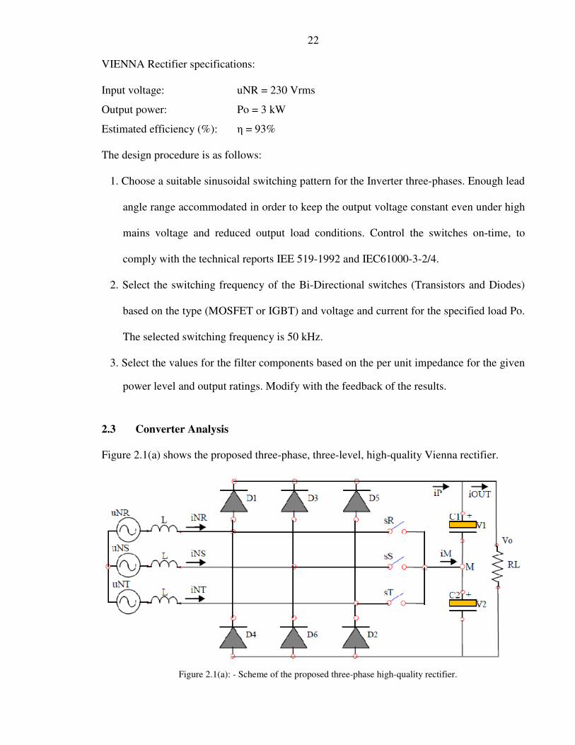
Figure 2.1(a) shows the proposed three-phase, three-level, high-quality Vienna rectifier.
Figure 2.1(a): - Scheme of the proposed three-phase high-quality rectifier.

23
This scheme is formally topologically similar to the Vienna rectifier the output capacitors are
C1 and C2. Each of the bi-directional switches sR, sS, sT can be built by using one switch
and one diode bridge rectifier or two switches and two diode rectifiers. All these components
are switched in such a manner that the EMI noise and the power losses are reduced and only
smaller magnetics are needed, thus saving cost and improving converter reliability.
Moreover, made sure only the standard high-frequency low-cost powdered iron-core type or
ferrite-core type input inductors are used.
2.4 System Simulation
At nominal output power level, it is possible to keep the output voltage constant for input low
voltage variations by making sure the input current is kept under the limits of the source
capacity. The switches on-time increased which in turn increases the boost effect. It is also
possible to compensate for input over-voltages provided the difference in potential of the
peak source voltage is reasonably lower than the maximum output voltage.
Apart from other benefits, the major benefit of this converter, as compared to simple bridge
rectifier with capacitor, is the input current harmonics reduction. Since this converter is
suitable for medium/high power applications, the harmonic limits described in the technical
report IEC 61000-3-4 as: “Limitation of emission of harmonic currents in low-voltage power
supply systems for equipment with rated current greater than 16 A per phase” are met.
Simulations have been performed in order to verify the input current harmonics at different
load levels while keeping the output voltage constant. Tabulated simulation results by
changing the loads on the output with R, RL and RL variable type and presented in the
following figures. The control strategy has enough lag and lead angle “δ” to keep the output
voltage stable, while keeping constant their sinusoidal PWM switching pattern.
24
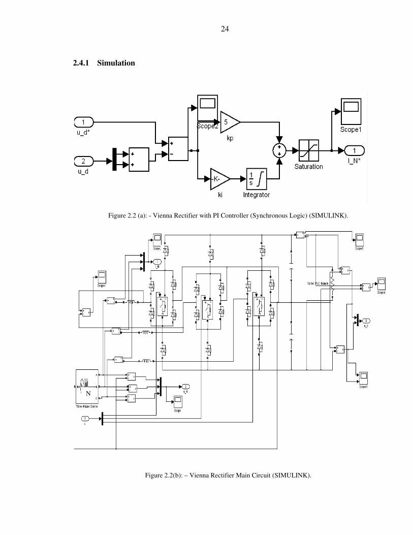
2.4.1 Simulation
Figure 2.2 (a): - Vienna Rectifier with PI Controller (Synchronous Logic) (SIMULINK).
Figure 2.2(b): – Vienna Rectifier Main Circuit (SIMULINK).
N
25
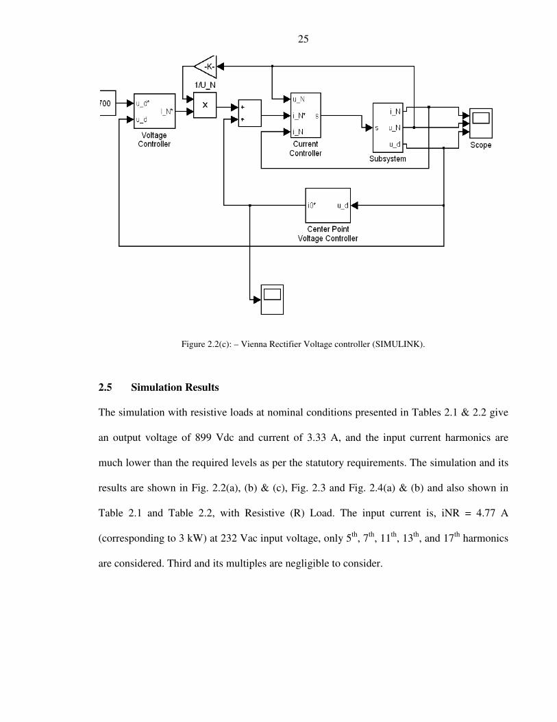
Figure 2.2(c): – Vienna Rectifier Voltage controller (SIMULINK).
2.5 Simulation Results
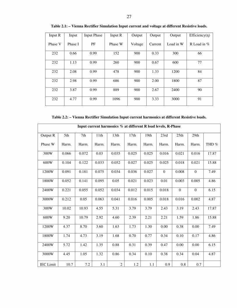
The simulation with resistive loads at nominal conditions presented in Tables 2.1 & 2.2 give
an output voltage of 899 Vdc and current of 3.33 A, and the input current harmonics are
much lower than the required levels as per the statutory requirements. The simulation and its
results are shown in Fig. 2.2(a), (b) & (c), Fig. 2.3 and Fig. 2.4(a) & (b) and also shown in
Table 2.1 and Table 2.2, with Resistive (R) Load. The input current is, iNR = 4.77 A
(corresponding to 3 kW) at 232 Vac input voltage, only 5th, 7th, 11th, 13th, and 17th harmonics
are considered. Third and its multiples are negligible to consider.
26
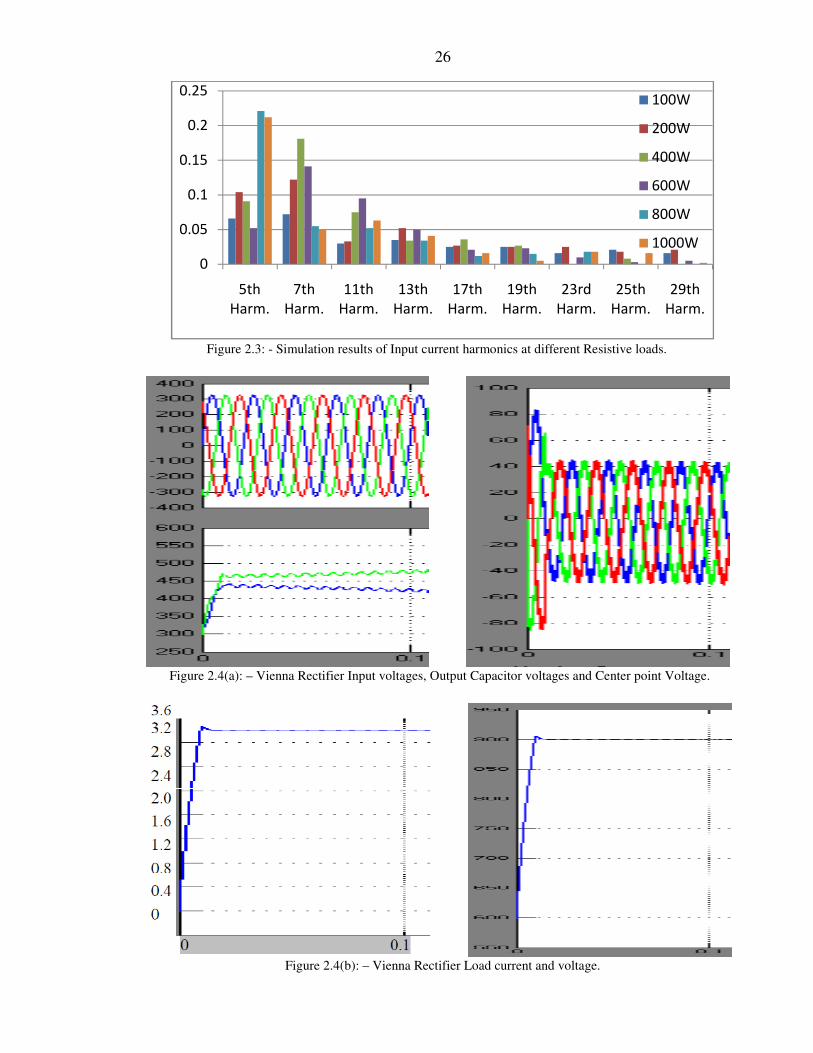
Figure 2.3: - Simulation results of Input current harmonics at different Resistive loads.
Figure 2.4(a): – Vienna Rectifier Input voltages, Output Capacitor voltages and Center point Voltage.
Figure 2.4(b): – Vienna Rectifier Load current and voltage.
0
0.05
0.1
0.15
0.2
0.25
5th
Harm.
7th
Harm.
11th
Harm.
13th
Harm.
17th
Harm.
19th
Harm.
23rd
Harm.
25th
Harm.
29th
Harm.
100W
200W
400W
600W
800W
1000W
27
Table 2.1: – Vienna Rectifier Simulation Input current and voltage at different Resistive loads.
Input R
Phase V
Input
Phase I
Input Phase
PF
Input R
Phase W
Output
Voltage
Output
Current
Output
Load in W
Efficiency(ƞ)
R Load in %
232 0.66 0.99 152 900 0.33 300 66
232 1.13 0.99 260 900 0.67 600 77
232 2.08 0.99 478 900 1.33 1200 84
232 2.98 0.99 686 900 2.00 1800 87
232 3.87 0.99 889 900 2.67 2400 90
232 4.77 0.99 1096 900 3.33 3000 91
Table 2.2: – Vienna Rectifier Simulation Input current harmonics at different Resistive loads.
Input current harmonics % at different R load levels, R-Phase
Output R
Phase W
5th
Harm.
7th
Harm.
11th
Harm.
13th
Harm.
17th
Harm.
19th
Harm.
23rd
Harm.
25th
Harm.
29th
Harm. THD %
300W 0.066 0.072 0.03 0.035 0.025 0.025 0.016 0.021 0.016 17.87
600W 0.104 0.122 0.033 0.052 0.027 0.025 0.025 0.018 0.021 15.88
1200W 0.091 0.181 0.075 0.034 0.036 0.027 0 0.008 0 7.49
1800W 0.052 0.141 0.095 0.05 0.021 0.023 0.01 0.003 0.005 4.86
2400W 0.221 0.055 0.052 0.034 0.012 0.015 0.018 0 0 6.15
3000W 0.212 0.05 0.063 0.041 0.016 0.005 0.018 0.016 0.002 4.87
300W 10.02 10.93 4.55 5.31 3.79 3.79 2.43 3.19 2.43 17.87
600W 9.20 10.79 2.92 4.60 2.39 2.21 2.21 1.59 1.86 15.88
1200W 4.37 8.70 3.60 1.63 1.73 1.30 0.00 0.38 0.00 7.49
1800W 1.74 4.73 3.19 1.68 0.70 0.77 0.34 0.10 0.17 4.86
2400W 5.72 1.42 1.35 0.88 0.31 0.39 0.47 0.00 0.00 6.15
3000W 4.45 1.05 1.32 0.86 0.34 0.10 0.38 0.34 0.04 4.87
IEC Limit 10.7 7.2 3.1 2 1.2 1.1 0.9 0.8 0.7
28
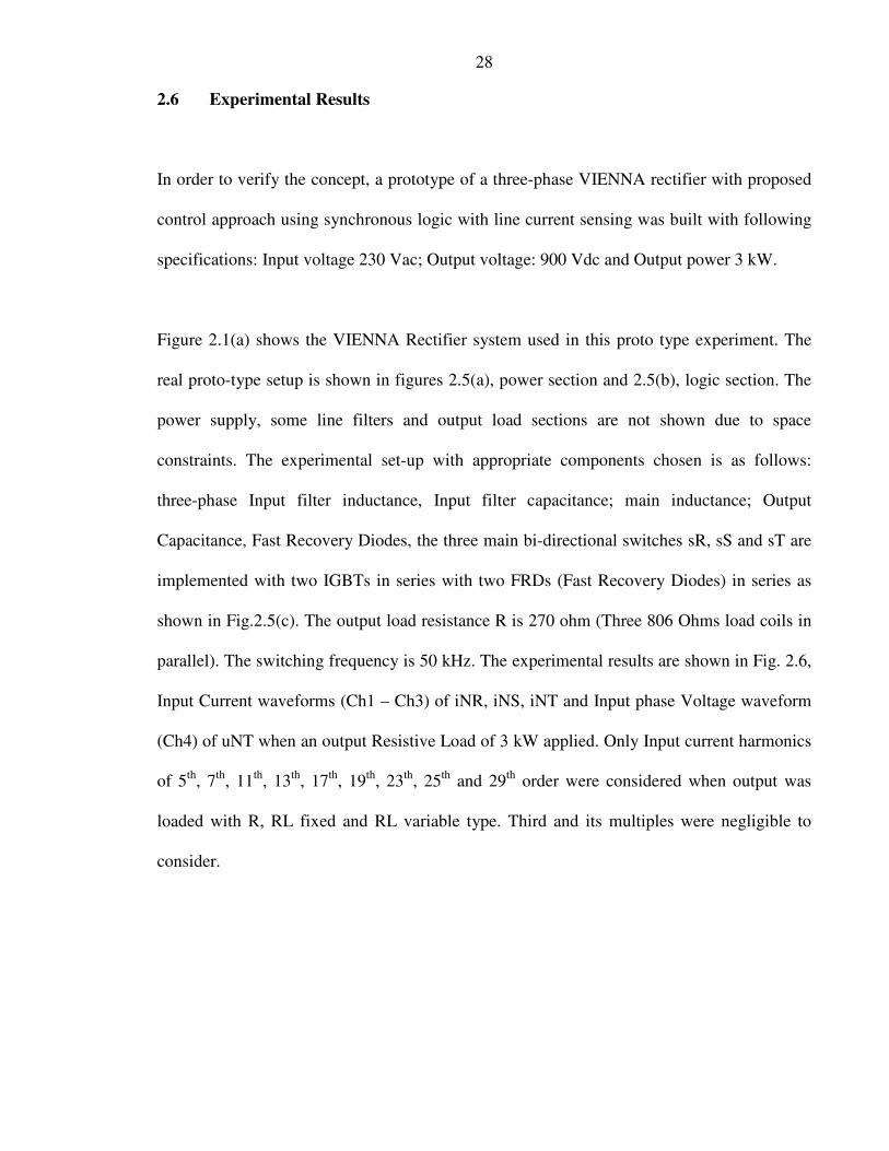
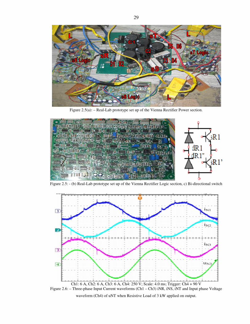
2.6 Experimental Results
In order to verify the concept, a prototype of a three-phase VIENNA rectifier with proposed
control approach using synchronous logic with line current sensing was built with following
specifications: Input voltage 230 Vac; Output voltage: 900 Vdc and Output power 3 kW.
Figure 2.1(a) shows the VIENNA Rectifier system used in this proto type experiment. The
real proto-type setup is shown in figures 2.5(a), power section and 2.5(b), logic section. The
power supply, some line filters and output load sections are not shown due to space
constraints. The experimental set-up with appropriate components chosen is as follows:
three-phase Input filter inductance, Input filter capacitance; main inductance; Output
Capacitance, Fast Recovery Diodes, the three main bi-directional switches sR, sS and sT are
implemented with two IGBTs in series with two FRDs (Fast Recovery Diodes) in series as
shown in Fig.2.5(c). The output load resistance R is 270 ohm (Three 806 Ohms load coils in
parallel). The switching frequency is 50 kHz. The experimental results are shown in Fig. 2.6,
Input Current waveforms (Ch1 – Ch3) of iNR, iNS, iNT and Input phase Voltage waveform
(Ch4) of uNT when an output Resistive Load of 3 kW applied. Only Input current harmonics
of 5th, 7th, 11th, 13th, 17th, 19th, 23th, 25th and 29th order were considered when output was
loaded with R, RL fixed and RL variable type. Third and its multiples were negligible to
consider.
29
Figure 2.5(a): – Real-Lab prototype set up of the Vienna Rectifier Power section.
Figure 2.5: - (b) Real-Lab prototype set up of the Vienna Rectifier Logic section, c) Bi-directional switch
Ch1: 6 A, Ch2: 6 A, Ch3: 6 A, Ch4: 250 V; Scale: 4.0 ms; Trigger: Ch4 + 90 V
Figure 2.6: – Three-phase Input Current waveforms (Ch1 – Ch3) iNR, iNS, iNT and Input phase Voltage
waveform (Ch4) of uNT when Resistive Load of 3 kW applied on output.
30
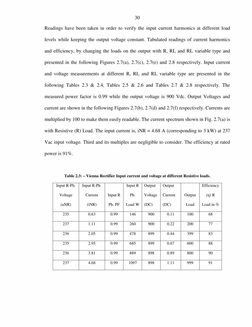
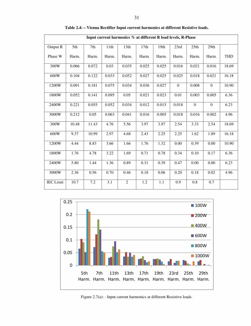
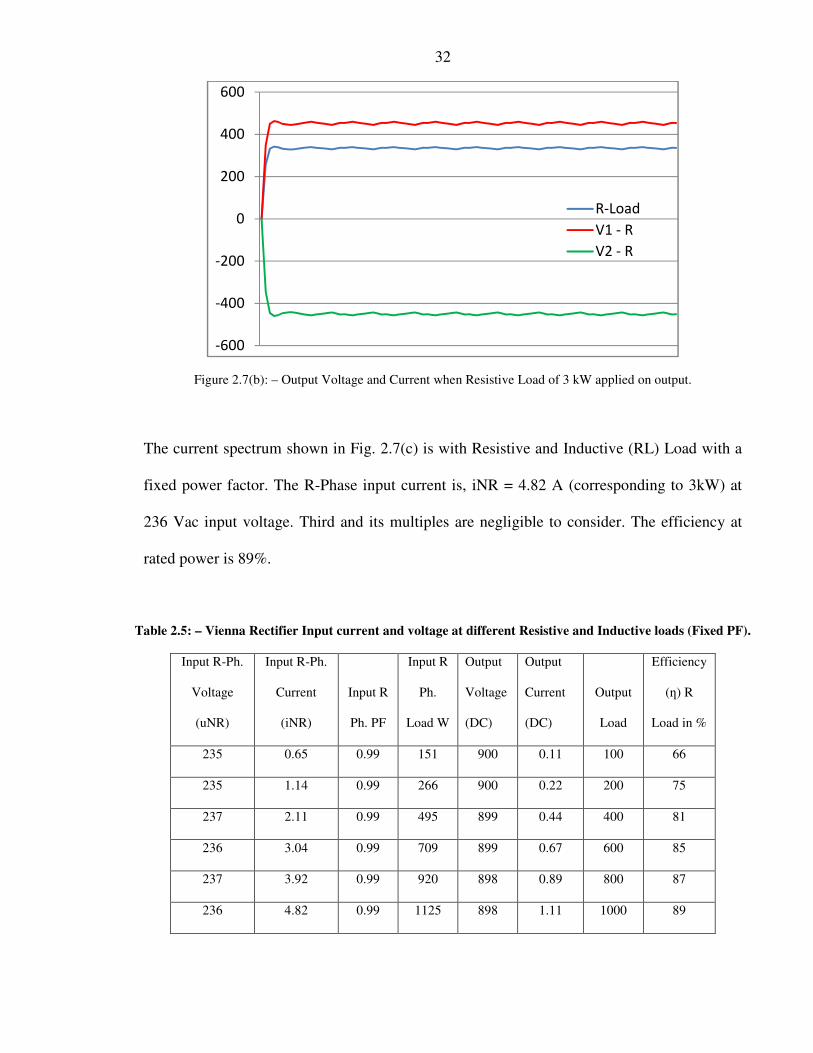
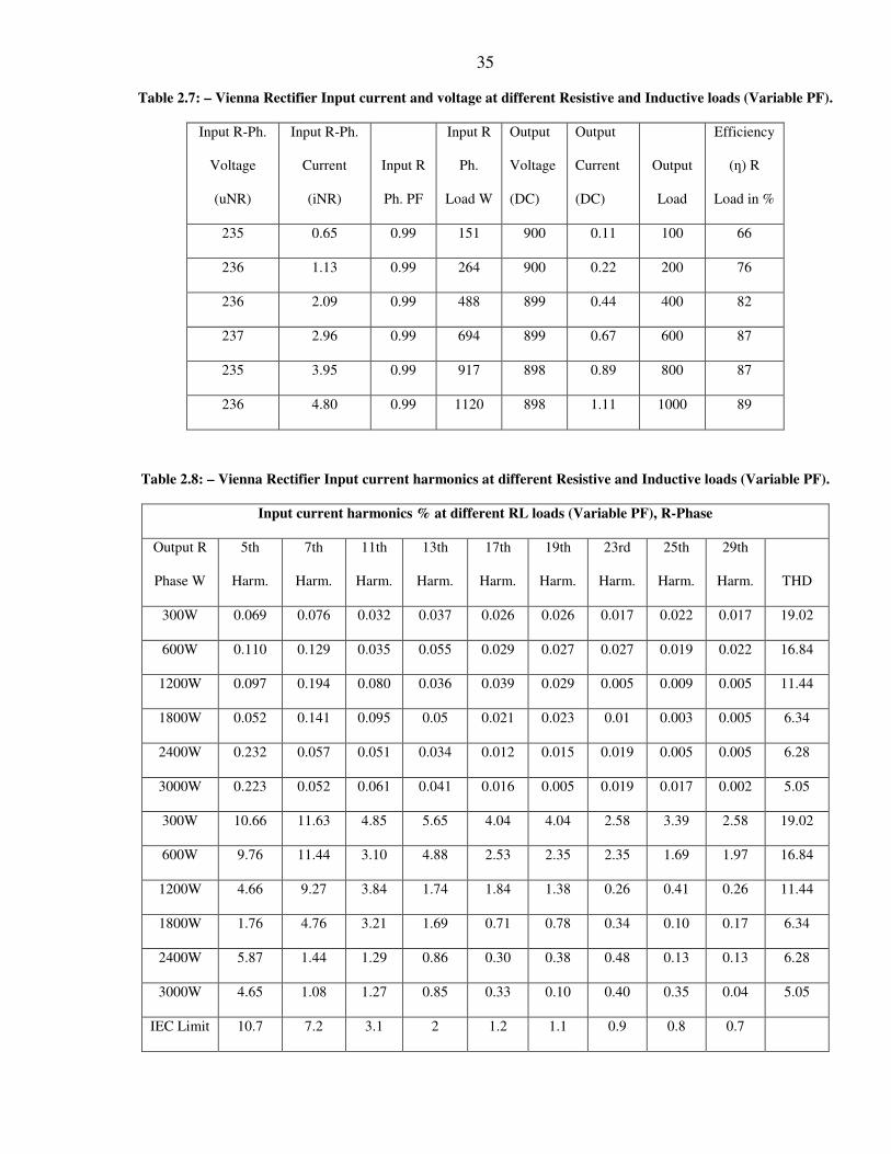
Readings have been taken in order to verify the input current harmonics at different load
levels while keeping the output voltage constant. Tabulated readings of current harmonics
and efficiency, by changing the loads on the output with R, RL and RL variable type and
presented in the following Figures 2.7(a), 2.7(c), 2.7(e) and 2.8 respectively. Input current
and voltage measurements at different R, RL and RL variable type are presented in the
following Tables 2.3 & 2.4, Tables 2.5 & 2.6 and Tables 2.7 & 2.8 respectively. The
measured power factor is 0.99 while the output voltage is 900 Vdc. Output Voltages and
current are shown in the following Figures 2.7(b), 2.7(d) and 2.7(f) respectively. Currents are
multiplied by 100 to make them easily readable. The current spectrum shown in Fig. 2.7(a) is
with Resistive (R) Load. The input current is, iNR = 4.68 A (corresponding to 3 kW) at 237
Vac input voltage. Third and its multiples are negligible to consider. The efficiency at rated
power is 91%.
Table 2.3: – Vienna Rectifier Input current and voltage at different Resistive loads.
Input R-Ph.
Voltage
(uNR)
Input R-Ph.
Current
(iNR)
Input R
Ph. PF
Input R
Ph.
Load W
Output
Voltage
(DC)
Output
Current
(DC)
Output
Load
Efficiency
(ƞ) R
Load in %
235 0.63 0.99 146 900 0.11 100 68
237 1.11 0.99 260 900 0.22 200 77
236 2.05 0.99 478 899 0.44 399 83
235 2.95 0.99 685 899 0.67 600 88
236 3.81 0.99 889 898 0.89 800 90
237 4.68 0.99 1097 898 1.11 999 91
31
Table 2.4: – Vienna Rectifier Input current harmonics at different Resistive loads.
Input current harmonics % at different R load levels, R-Phase
Output R
Phase W
5th
Harm.
7th
Harm.
11th
Harm.
13th
Harm.
17th
Harm.
19th
Harm.
23rd
Harm.
25th
Harm.
29th
Harm. THD
300W 0.066 0.072 0.03 0.035 0.025 0.025 0.016 0.021 0.016 18.69
600W 0.104 0.122 0.033 0.052 0.027 0.025 0.025 0.018 0.021 16.18
1200W 0.091 0.181 0.075 0.034 0.036 0.027 0 0.008 0 10.90
1800W 0.052 0.141 0.095 0.05 0.021 0.023 0.01 0.003 0.005 6.36
2400W 0.221 0.055 0.052 0.034 0.012 0.015 0.018 0 0 6.23
3000W 0.212 0.05 0.063 0.041 0.016 0.005 0.018 0.016 0.002 4.96
300W 10.48 11.43 4.76 5.56 3.97 3.97 2.54 3.33 2.54 18.69
600W 9.37 10.99 2.97 4.68 2.43 2.25 2.25 1.62 1.89 16.18
1200W 4.44 8.83 3.66 1.66 1.76 1.32 0.00 0.39 0.00 10.90
1800W 1.76 4.78 3.22 1.69 0.71 0.78 0.34 0.10 0.17 6.36
2400W 5.80 1.44 1.36 0.89 0.31 0.39 0.47 0.00 0.00 6.23
3000W 2.36 0.56 0.70 0.46 0.18 0.06 0.20 0.18 0.02 4.96
IEC Limit 10.7 7.2 3.1 2 1.2 1.1 0.9 0.8 0.7
Figure 2.7(a): - Input current harmonics at different Resistive loads.
0
0.05
0.1
0.15
0.2
0.25
5th
Harm.
7th
Harm.
11th
Harm.
13th
Harm.
17th
Harm.
19th
Harm.
23rd
Harm.
25th
Harm.
29th
Harm.
100W
200W
400W
600W
800W
1000W
32
Figure 2.7(b): – Output Voltage and Current when Resistive Load of 3 kW applied on output.
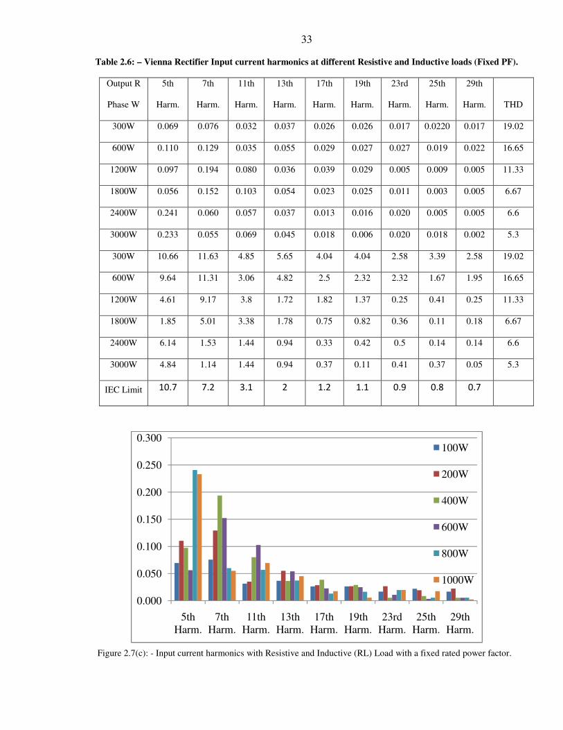
The current spectrum shown in Fig. 2.7(c) is with Resistive and Inductive (RL) Load with a
fixed power factor. The R-Phase input current is, iNR = 4.82 A (corresponding to 3kW) at
236 Vac input voltage. Third and its multiples are negligible to consider. The efficiency at
rated power is 89%.
Table 2.5: – Vienna Rectifier Input current and voltage at different Resistive and Inductive loads (Fixed PF).
Input R-Ph.
Voltage
(uNR)
Input R-Ph.
Current
(iNR)
Input R
Ph. PF
Input R
Ph.
Load W
Output
Voltage
(DC)
Output
Current
(DC)
Output
Load
Efficiency
(ƞ) R
Load in %
235 0.65 0.99 151 900 0.11 100 66
235 1.14 0.99 266 900 0.22 200 75
237 2.11 0.99 495 899 0.44 400 81
236 3.04 0.99 709 899 0.67 600 85
237 3.92 0.99 920 898 0.89 800 87
236 4.82 0.99 1125 898 1.11 1000 89
-600
-400
-200
0
200
400
600
R-Load
V1 - R
V2 - R
33
Table 2.6: – Vienna Rectifier Input current harmonics at different Resistive and Inductive loads (Fixed PF).
Output R
Phase W
5th
Harm.
7th
Harm.
11th
Harm.
13th
Harm.
17th
Harm.
19th
Harm.
23rd
Harm.
25th
Harm.
29th
Harm. THD
300W 0.069 0.076 0.032 0.037 0.026 0.026 0.017 0.0220 0.017 19.02
600W 0.110 0.129 0.035 0.055 0.029 0.027 0.027 0.019 0.022 16.65
1200W 0.097 0.194 0.080 0.036 0.039 0.029 0.005 0.009 0.005 11.33
1800W 0.056 0.152 0.103 0.054 0.023 0.025 0.011 0.003 0.005 6.67
2400W 0.241 0.060 0.057 0.037 0.013 0.016 0.020 0.005 0.005 6.6
3000W 0.233 0.055 0.069 0.045 0.018 0.006 0.020 0.018 0.002 5.3
300W 10.66 11.63 4.85 5.65 4.04 4.04 2.58 3.39 2.58 19.02
600W 9.64 11.31 3.06 4.82 2.5 2.32 2.32 1.67 1.95 16.65
1200W 4.61 9.17 3.8 1.72 1.82 1.37 0.25 0.41 0.25 11.33
1800W 1.85 5.01 3.38 1.78 0.75 0.82 0.36 0.11 0.18 6.67
2400W 6.14 1.53 1.44 0.94 0.33 0.42 0.5 0.14 0.14 6.6
3000W 4.84 1.14 1.44 0.94 0.37 0.11 0.41 0.37 0.05 5.3
IEC Limit 10.7 7.2 3.1 2 1.2 1.1 0.9 0.8 0.7
Figure 2.7(c): - Input current harmonics with Resistive and Inductive (RL) Load with a fixed rated power factor.
0.000
0.050
0.100
0.150
0.200
0.250
0.300
5th Harm.
7th Harm.
11th Harm.
13th Harm.
17th Harm.
19th Harm.
23rd Harm.
25th Harm.
29th Harm.
100W
200W
400W
600W
800W
1000W
34
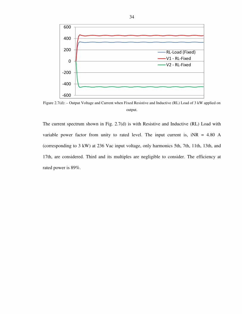
Figure 2.7(d): – Output Voltage and Current when Fixed Resistive and Inductive (RL) Load of 3 kW applied on
output.
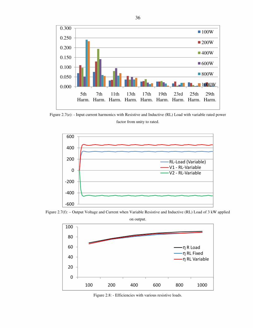
The current spectrum shown in Fig. 2.7(d) is with Resistive and Inductive (RL) Load with
variable power factor from unity to rated level. The input current is, iNR = 4.80 A
(corresponding to 3 kW) at 236 Vac input voltage, only harmonics 5th, 7th, 11th, 13th, and
17th, are considered. Third and its multiples are negligible to consider. The efficiency at
rated power is 89%.
-600
-400
-200
0
200
400
600
RL-Load (Fixed)
V1 - RL-Fixed
V2 - RL-Fixed
35
Table 2.7: – Vienna Rectifier Input current and voltage at different Resistive and Inductive loads (Variable PF).
Input R-Ph.
Voltage
(uNR)
Input R-Ph.
Current
(iNR)
Input R
Ph. PF
Input R
Ph.
Load W
Output
Voltage
(DC)
Output
Current
(DC)
Output
Load
Efficiency
(ƞ) R
Load in %
235 0.65 0.99 151 900 0.11 100 66
236 1.13 0.99 264 900 0.22 200 76
236 2.09 0.99 488 899 0.44 400 82
237 2.96 0.99 694 899 0.67 600 87
235 3.95 0.99 917 898 0.89 800 87
236 4.80 0.99 1120 898 1.11 1000 89
Table 2.8: – Vienna Rectifier Input current harmonics at different Resistive and Inductive loads (Variable PF).
Input current harmonics % at different RL loads (Variable PF), R-Phase
Output R
Phase W
5th
Harm.
7th
Harm.
11th
Harm.
13th
Harm.
17th
Harm.
19th
Harm.
23rd
Harm.
25th
Harm.
29th
Harm. THD
300W 0.069 0.076 0.032 0.037 0.026 0.026 0.017 0.022 0.017 19.02
600W 0.110 0.129 0.035 0.055 0.029 0.027 0.027 0.019 0.022 16.84
1200W 0.097 0.194 0.080 0.036 0.039 0.029 0.005 0.009 0.005 11.44
1800W 0.052 0.141 0.095 0.05 0.021 0.023 0.01 0.003 0.005 6.34
2400W 0.232 0.057 0.051 0.034 0.012 0.015 0.019 0.005 0.005 6.28
3000W 0.223 0.052 0.061 0.041 0.016 0.005 0.019 0.017 0.002 5.05
300W 10.66 11.63 4.85 5.65 4.04 4.04 2.58 3.39 2.58 19.02
600W 9.76 11.44 3.10 4.88 2.53 2.35 2.35 1.69 1.97 16.84
1200W 4.66 9.27 3.84 1.74 1.84 1.38 0.26 0.41 0.26 11.44
1800W 1.76 4.76 3.21 1.69 0.71 0.78 0.34 0.10 0.17 6.34
2400W 5.87 1.44 1.29 0.86 0.30 0.38 0.48 0.13 0.13 6.28
3000W 4.65 1.08 1.27 0.85 0.33 0.10 0.40 0.35 0.04 5.05
IEC Limit 10.7 7.2 3.1 2 1.2 1.1 0.9 0.8 0.7
36
Figure 2.7(e): - Input current harmonics with Resistive and Inductive (RL) Load with variable rated power
factor from unity to rated.
Figure 2.7(f): – Output Voltage and Current when Variable Resistive and Inductive (RL) Load of 3 kW applied
on output.
Figure 2.8: - Efficiencies with various resistive loads.
0.000
0.050
0.100
0.150
0.200
0.250
0.300
5th Harm.
7th Harm.
11th Harm.
13th Harm.
17th Harm.
19th Harm.
23rd Harm.
25th Harm.
29th Harm.
100W
200W
400W
600W
800W
1000W
-600
-400
-200
0
200
400
600
RL-Load (Variable)
V1 - RL-Variable
V2 - RL-Variable
0
20
40
60
80
100
100 200 400 600 800 1000
ƞ R Load
ƞ RL Fixed
ƞ RL Variable
37
The efficiencies shown in Fig. 2.8 are with Resistive, Resistive and Inductive (RL) Load with
fixed power factor and with variable power factor from unity to rated. Measurements were
tabulated by changing the loads on the output of the setup. The efficiency varied based on the
type of load and also percentage of the load from 66% to 91%.
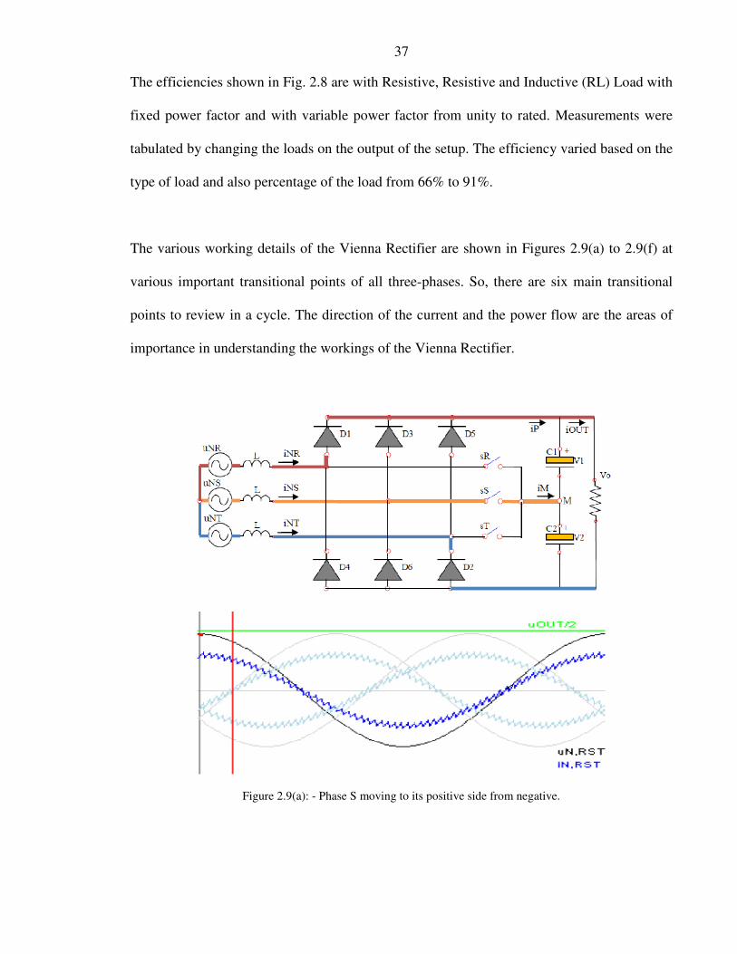
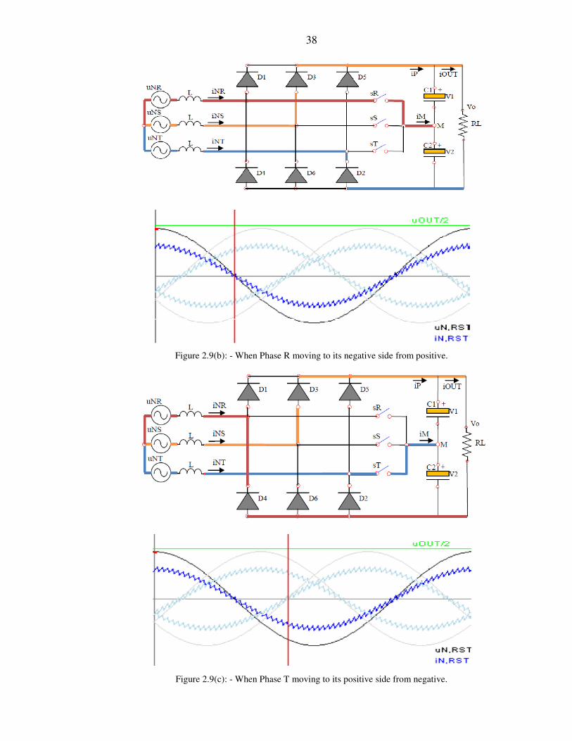
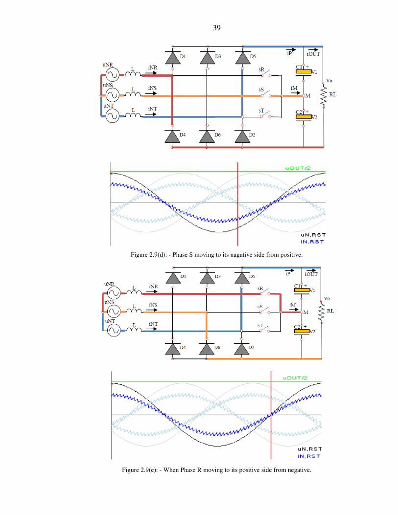
The various working details of the Vienna Rectifier are shown in Figures 2.9(a) to 2.9(f) at
various important transitional points of all three-phases. So, there are six main transitional
points to review in a cycle. The direction of the current and the power flow are the areas of
importance in understanding the workings of the Vienna Rectifier.
Figure 2.9(a): - Phase S moving to its positive side from negative.
38
Figure 2.9(b): - When Phase R moving to its negative side from positive.
Figure 2.9(c): - When Phase T moving to its positive side from negative.
39
Figure 2.9(d): - Phase S moving to its nagative side from positive.
Figure 2.9(e): - When Phase R moving to its positive side from negative.
40
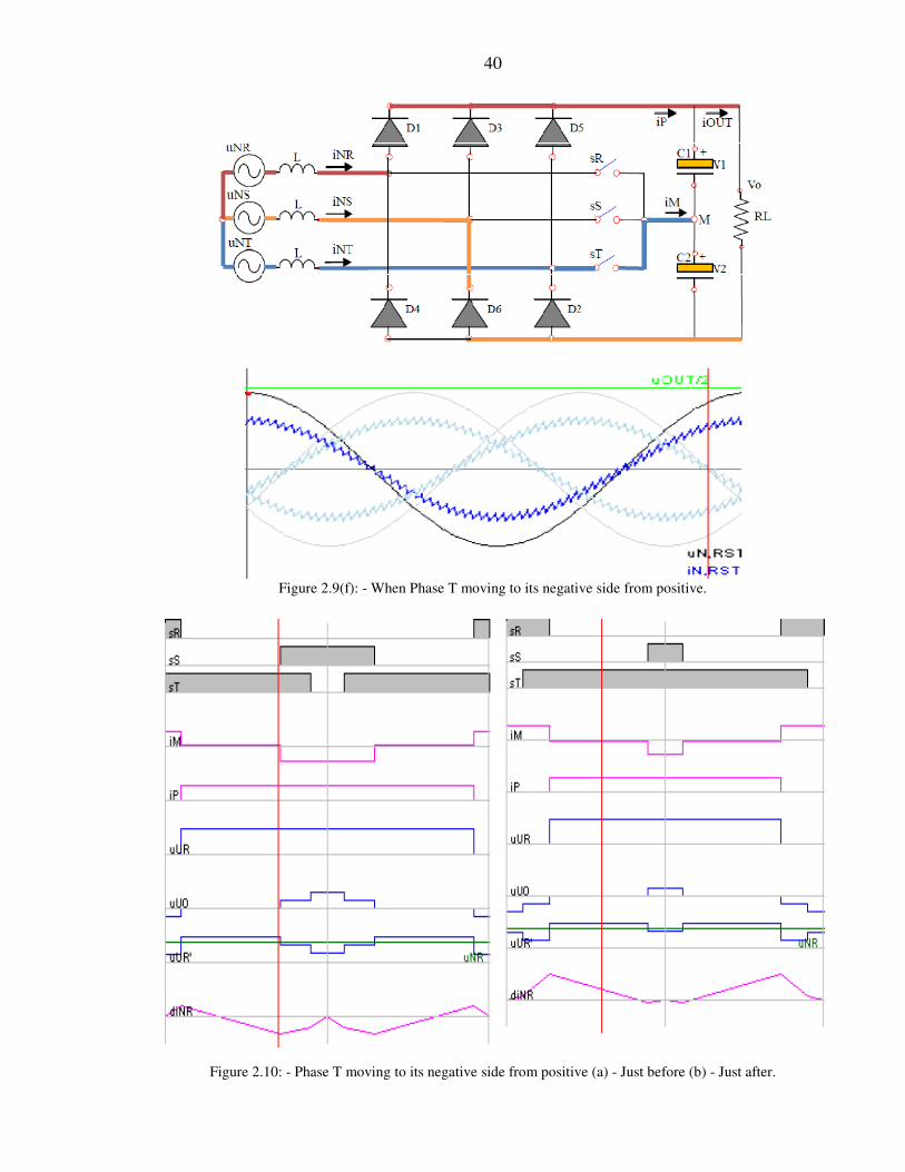
Figure 2.9(f): - When Phase T moving to its negative side from positive.
Figure 2.10: - Phase T moving to its negative side from positive (a) - Just before (b) - Just after.

41
Details of various switch conditions; voltage and current waveforms are shown in Figures
2.10(a) and 2.10(b), just before and just after phase T moving to its nagative side from
positive side respectively.
2.7 Summary
The proposed three-phase three-switch three-level (VIENNA) rectifier circuit with unity
power factor was investigated and was able to control current distortion that was generally
generated by diode bridge rectifiers and capacitive filter. A new three-phase synchronous
logic control simulations showed that it could produce very low output voltage ripple and
very low input current harmonics with unity power factor. The resulting current harmonics
were below the statutory limits of IEC 61000-3-4 at different load level. It was also possible
to compensate for input over-voltage just by adjusting the control signals to bidirectional
switches.
An experimental prototype system of 3 kW VIENNA rectifier was built to verify the concept.
Near unity power factor was measured in all three-phases. The proposed control logic was
implemented by sensing input voltages, input currents, output currents and output voltage.
The controller was very simple and reliable. The inductance value was reduced and also
small in size when compared to the only passive filter circuit. The experimental results
confirm the designed proto-type circuit’s behavior.