Embed Size (px)
Citation preview

MIT MYSORE DEPT.OF ELECTRONICS AND COMMUNICATION ENGG
1 Analog Electronics Lab 17ECL37
EXPERIMENT-1
FULL WAVE RECTIFIER AND BRIDGE RECTIFIER
AIM:
1. To construct full wave rectifier and bridge rectifier with and without capacitor
filter in order to have rectified, filtered output dc voltage.
2. To calculate efficiency, percentage regulation and ripple factor.
COMPONENTS REQUIRED:
Sl. No Component/ IC/Device
/Equipment
Specification /Value Number/Quantity
1 Transformer 230V,50Hz/ 15 V, 50 HZ 01
2 Decade Resistance Box -- 01
3 Diodes BY127/IN4001 04
4 Capacitors 470 μF 01
5 Ammeter 0-500mA 01
6 Voltmeter 0- 30V 01
Center Tapped Full Wave Rectifier:
Theory:
The circuit of a center tapped full wave rectifier uses two diodes D1&D2. During
positive half cycle of secondary voltage, the diode D1 is forward biased and D2 is
reverse biased. The diode D1 conducts and current flows through load resistor RL.
During negative half cycle, diode D2 becomes forward biased and D1 reverse biased.
Now D2 conducts and current flows through the load resistor RL, during both the half
cycles and will get unidirectional current as shown in the model graph. The difference
between full wave and half wave rectification is that a full wave rectifier allows
unidirectional current to the load during the entire 360 degrees of the input signal and
half wave rectifier allows this only during one half cycle (180 degrees).
Procedure:
Without C filter:
1. Make the Connections as shown in the circuit diagram.
2. Switch on the Supply.
3. Observe the input and output waveforms of the rectifier and note down the output DC and
AC voltages (Vdc and Vac).
4. Observe the Voltage across the secondary of the Transformer (i.e Vrms). Calculate
the ripple factor, efficiency and percentage regulation at the output.

MIT MYSORE DEPT.OF ELECTRONICS AND COMMUNICATION ENGG
2 Analog Electronics Lab 17ECL37
Full wave rectifier with
center tapped transformer
without filter
Waveform:
Vm
Full wave rectifier with center tapped transformer with filter
Waveform:

MIT MYSORE DEPT.OF ELECTRONICS AND COMMUNICATION ENGG
3 Analog Electronics Lab 17ECL37
Calculations: From C.R.O. observations:
Vrms = Vm/2 =
Vdc =2Vm/π=
Vac = (Vrms2-Vdc2) =
r = Vac/Vdc= Vdc(NL)=
Percentage Regulation= (Vdc(NL) - Vdc(FL))×100/ Vdc(FL)=
Efficiency = η =( Pdc / Prms) ×100 = (Vdc/Vrms)2×100=
With C filter:
Connect a capacitor filter in parallel with load resistor and repeat the same procedure listed
above.
Shunt capacitor filter in FWR - r = 1/(43fRLC)
Vdc
(v)
VRMS
(v)
Idc
(A)
IRMS
(A)
Resistance
(Ω)
Efficiency
(η)
Ripple factor
(r)
%Regulation
Vdc
(v)
VRMS
(v)
Idc
(A)
IRMS
(A)
Resistance
(Ω)
Efficiency
(η)
Ripple factor
(r)
%Regulation

MIT MYSORE DEPT.OF ELECTRONICS AND COMMUNICATION ENGG
4 Analog Electronics Lab 17ECL37
Bridge rectifier without C filter
Tabular column without C filter
Bridge rectifier circuit with C filter
Tabular column with C filter
Vdc
(v)
VRMS
(v)
Idc
(A)
IRMS
(A)
Resistance
(Ω)
Efficiency
(η)
Ripple factor
(r)
%Regulation
Vdc
(v)
VRMS
(v)
Idc
(A)
IRMS
(A)
Resistance
(Ω)
Ripple factor
(r)
%Regulation

MIT MYSORE DEPT.OF ELECTRONICS AND COMMUNICATION ENGG
5 Analog Electronics Lab 17ECL37
Result:

MIT MYSORE DEPT.OF ELECTRONICS AND COMMUNICATION ENGG
6 Analog Electronics Lab 17ECL37

MIT MYSORE DEPT.OF ELECTRONICS AND COMMUNICATION ENGG
7 Analog Electronics Lab 17ECL37
EXPERIMENT-02
DIODE CLIPPING AND CLAMPING CIRCUITS
AIM: To design the different types of Clipping and Clamping Circuits and also to obtain
the transfer characteristics for the same.
Equipment and components:
SL.NO NAME OF EQUIPMENTS/
COMPONENTS
SPECIFICATIONS QTY
1. Dual Power Supply Variable 0 – 30 V / 2 Amp D.C. 01
2. Function Generator 0 – 3 MHz, 0 – 20 V(p-p) 01
3. CRO Analog, 30 MHz, Dual Channel 01
4. Connecting Board 01
5. Resistance 10 KΩ (½ Watt) 01
6. CRO Probe -- 03
7. Diode 1N4007 02
8. Patch cords, Connecting Wires, etc.
THEORY: Refer Text Book Electronic Devices And Circuit Theory By Robert L.
Boylestad / Louis Nashelsky “chapter 2 “
Procedure:
1. Circuit is wired up as shown in Fig.(1) and a sinusoidal signal of 1 KHz and
amplitude of 10 V(p-p) (Peak amplitude should be greater than clipping
level) is applied at input Vi.
2. Observe output signal on the CRO and verify it with the given waveforms.
3. Apply Vi and Vo to the X and Y channel of CRO and transfer characteristics is
obtained using X – Y mode in CRO.
Inference: ____________________

MIT MYSORE DEPT.OF ELECTRONICS AND COMMUNICATION ENGG
8 Analog Electronics Lab 17ECL37
1. Diode Shunt Clipping above Vr (reference voltage) or Positive Peak Clipping
Circuit.
Fig. (1) Circuit Diagram of Diode Shunt Input output Waveforms Transfer
Characteristic Clipping above Vr
Rf =10 Ω (Forward Resistance of Diode)
Rr =10 KΩ (Reverse Resistance of Diode)
Design:
The output to be clipped above 2 V.
So Vo (max) = +2 V
From the Fig. (1)
Vo = Vo (max) – Vr + Vref
Where Vr is Diode drop which is nearly equal to 0.6 V.
So Vref = Vo (max) – Vr
= 2 – 0.6 = 1.4 V
Select the input amplitude more than 3Volts.
R = 10 KΩ

MIT MYSORE DEPT.OF ELECTRONICS AND COMMUNICATION ENGG
9 Analog Electronics Lab 17ECL37
2. Diode Shunt Clipping below Vr (reference voltage) or Negative Peak Clipping
Circuit.
Fig. (2) Circuit Diagram of Diode Input output Waveforms Transfer Characteristic
Shunt Clipping below Vr
Design: Output voltage be clipped at + 2 Volt.
Vo (max) = Vref = 2 V
R = 10KΩ
Procedure:
1. Circuit is wired up as shown in Fig. (2) and a sinusoidal signal of 1 KHz and
amplitude of 10V (p-p) (Peak amplitude should be greater than clipping level) is
applied at input.
2. Observe output signal on the CRO and verify it with the given waveforms.
3. Apply Vi and Vo to the X and Y channel of CRO and transfer characteristics is
obtained using X – Y mode in CRO.
Inference: ____________________

MIT MYSORE DEPT.OF ELECTRONICS AND COMMUNICATION ENGG
10 Analog Electronics Lab 17ECL37
3. Clipping two independent level or slicer
Fig. (5) Circuit Diagram Input output Waveforms Transfer Characteristic
Design: To clipping the signal below 2 Volt and above 4 Volt levels
Let VR1 > VR2
1] Vo max = 4 V, i.e. Vo max = VR1 + Vr
VR1 = Vo max – Vr
= 4 – 0.6
so
2] Vo min = 2 V i.e. Vo min = VR2 – Vr
VR2 = Vo min + Vr
= 2 + 0.6
Procedure:
1. Circuit is wired up as shown in Fig. (5) and a sinusoidal signal of 1 KHz and a
suitable amplitude (Peak amplitude should be greater than clipping level) is
applied at input Vi.
2. Observe output signal on the CRO and verify it with the given waveforms.
3. Apply Vi and Vo to the X and Y channel of CRO and transfer characteristics is
obtained using X – Y mode in CRO.
VR1 = 3.4 V
VR2 = 2.6 V R = 10KΩ

MIT MYSORE DEPT.OF ELECTRONICS AND COMMUNICATION ENGG
11 Analog Electronics Lab 17ECL37
Inference: _______________
4. Double ended clipper to generate a symmetrical square wave or squarer
Fig. (6) Circuit Diagram of Double ended Input output Waveform Transfer Characteristic
Clipper or squarer
Design: To generate a symmetrical square wave
Vref =± 4 Volts
i.e. VR = VR1 = VR2 = Vref = 4 Volts
Vo max = VR + Vr
VR = Vo max - Vr = 4 – 0.6
Procedure:
1. Circuit is wired up as shown in Fig.(6) and a sinusoidal signal of 1 KHz and a
suitable amplitude (Peak amplitude should be greater than clipping level) is
applied at input Vi.
2. Observe output signal on the CRO and verify it with the given waveforms.
3. Apply Vi and Vo to the X and Y channel of CRO and transfer characteristics is
obtained using X – Y mode in CRO.
Inference: _______________
VR = 3.4 V R = 10KΩ

MIT MYSORE DEPT.OF ELECTRONICS AND COMMUNICATION ENGG
12 Analog Electronics Lab 17ECL37

MIT MYSORE DEPT.OF ELECTRONICS AND COMMUNICATION ENGG
13 Analog Electronics Lab 17ECL37
Clamping Circuits:
1] Positive peak or negative clamping:
Fig. (1) Circuit Diagram of Positive Peak Clamping Circuit
Design:
Clamping circuit to clamp positive peak at +3V.The input waveform has a frequency of 1
KHz sine wave or square wave with suitable amplitude.
Vo max = Vref + Vr
Vref = Vo max – Vr = 3 – 0.6
Given frequency 1 KHz
So 3101
1
T
= 1mSec
RC = 10 T
RC = (10) 1mSec = 10 mSec
C = 10 mSec / 10 K = 1µF
Vref = 2.4 V
Choose RC » T
R = 10 KΩ

MIT MYSORE DEPT.OF ELECTRONICS AND COMMUNICATION ENGG
14 Analog Electronics Lab 17ECL37
Fig. (2) Input and Output waveforms of a positive Peak Clamping Circuit
Note: Set Vref = 0 and observe the output for both sine and square wave input.
Procedure:
1] Positive Clamping Circuit;
a) Connect the circuit as shown in Fig. (1)
b) Apply input sinusoidal signal of amplitude 12 V p-p and frequency of 1 KHz
[Amplitude of input signal must be greater than clamping level]
C) Connect the output to CRO in DC Mode and compare the output with the given
waveforms.
d) For the same circuit, give a square wave input and observe the output and
compare output with given waveforms
e) Make Vref = 0 and observe the output.
f) Observe the output in DC mode of CRO
3V
0

MIT MYSORE DEPT.OF ELECTRONICS AND COMMUNICATION ENGG
15 Analog Electronics Lab 17ECL37
2] Negative peak or positive clamping:
Fig. (3) Circuit Diagram of Negative Peak Clamping Circuit
Design:
Clamping Circuit to clamp Negative peak of the output voltage at -3V
Vo min = Vref - Vr
Vref = Vo min + Vr = -3 + 0.6
Fig.(4) Input and Output waveforms of a Negative Peak Clamping Circuit.
Note: Set Vref = 0 and observe the output for both sine and square wave input.
Vref = -2.4 V
0 0

MIT MYSORE DEPT.OF ELECTRONICS AND COMMUNICATION ENGG
16 Analog Electronics Lab 17ECL37
Procedure:
2] Negative Clamping Circuit;
a) Connect the circuit as shown in Fig. (3)
b) Apply input sinusoidal signal of amplitude 12 V(p-p) and frequency of 1 KHz
[Peak amplitude of input signal must be greater than clamping level]
C) Connect the output to CRO in DC Mode and compare the output with the given
waveforms.
d) For the same circuit, give a square input and observe the output and compare
output with given waveforms.
e) Make Vref = 0 and observe the output.
Inference: ________________
Probable viva questions:
1) What are clipping and clamping circuits
2) What is the difference between clipping and clamping circuits
3) What are the components of clipping circuit
4) What are the types of clipping circuit
5) Sketch the transfer characteristics of double ended clipper circuit
6) What are the applications of clipper and clamper circuits
7) Write the different equivalent circuits of a diode
10) What is diffusion and transition capacitance?
11) Define reverse recovery time of a diode
12) Explain the diode current equation

MIT MYSORE DEPT.OF ELECTRONICS AND COMMUNICATION ENGG
17 Analog Electronics Lab 17ECL37
EXPERIMENT-03
SERIES VOLTAGE REGULATOR
AIM: To study and verify the functionality of Zener diode in forward bias and reverse
bias and to
1. Plot Volt-Ampere Characteristics of Zener Diode.
2. Find Zener Breakdown Voltage in Reverse Biased conditions.
3. Calculate static and dynamic resistance of the Zener diode in both forward and
reverse biased conditions (before, after break down voltages).
Components Required:
S.No. Name Quantity
1 Zener Diodes (1N4735A) 1(One) No.
2 Resistors (1K , 3.3 ) 1(One) No. Each
3 Bread board 1(One) No.
Equipment:
S.No. Name Quantity
1 Dual DC Regulated power supply (0 - 30V) 1(One) No.
2 Digital Ammeter (0 - 200 mA) 2(Two) No.
3 Digital Voltmeter (0 - 20V) 1(One) No.
4 Decade Resistance Box (DRB) 1(One) No.
5 Connecting wires (Single Strand)
Specifications of 1N 4735A Zener diode:
Breakdown Voltage = 5.1V
Power dissipation = 0.75W
Max Forward Current = 1A

MIT MYSORE DEPT.OF ELECTRONICS AND COMMUNICATION ENGG
18 Analog Electronics Lab 17ECL37
Operation:
Zener diodes are a special kind of diode which permits current to flow in the
forward direction. What makes them different from other diodes is that Zener diodes
will also allow current to flow in the reverse direction when the voltage is above a
certain value. This breakdown voltage is known as the Zener voltage. In a standard
diode, the Zener voltage is high, and the diode is permanently damaged if a reverse
current above that value is allowed to pass through it. Zener diodes are designed in a
way where the Zener voltage is a much lower value. There is a controlled breakdown
which does not damage the diode when a reverse current above the Zener voltage
passes through a Zener diode.
The most common values for nominal working voltage are 5.1 V, 5.6 V, 6.2 V, 12
V and 15 V. We also carry Zener diodes with nominal working voltage up to 1 kV.
Forward (drive) current can have a range from 200 uA to 200 A, with the most common
forward (drive) current being 10 mA or 200 mA. In the forward bias direction, the
Zener diode behaves like an ordinary silicon diode.
In the reverse bias direction, there is practically no reverse current flow until the
breakdown voltage is reached. When this occurs there is a sharp increase in reverse
current. Varying amount of reverse current can pass through the diode without
damaging it. The breakdown voltage or Zener voltage (VZ) across the diode remains
relatively constant. The maximum reverse current is limited, however, by the wattage
rating of the diode.
Avalanche Break down:
When the diode is in the reverse bias condition, the width of the depletion region
is more. If both p-side and n-side of the diode are lightly doped, depletion region at the
junction widens. In reverse bias, the minority charge carrier current flows through
junction. As the applied reverse voltage increases the minority carriers acquire
sufficient energy to collide with the carriers in the covalent bonds inside the depletion
region. As a result, the bond breaks and electron hole pairs are generated. The process
becomes cumulative and leads to the generation of a large number of charge carriers
resulting in Avalanche Breakdown.

MIT MYSORE DEPT.OF ELECTRONICS AND COMMUNICATION ENGG
19 Analog Electronics Lab 17ECL37
Zener Break down:
If both p-side and n-side of the diode are heavily doped, depletion region at the
junction reduces compared to the width in normal doping. Applying a reverse bias
causes a strong electric field get applied across the device. As the reverse bias is
increased, the Electric field becomes strong enough to rupture covalent bonds and
generate large number of charge carriers. Such sudden increase in the number of
charge carriers due to rupture of covalent bonds under the influence of strong electric
field is termed as Zener breakdown.
Zener Diode as Voltage Regulator:
The function of a regulator is to provide a constant output voltage to a load
connected in parallel with it in spite of the ripples in the supply voltage or the variation
in the load current and the Zener diode will continue to regulate the voltage until the
diodes current falls below the minimum IZ(min) value in the reverse breakdown region.
It permits current to flow in the forward direction as normal, but will also allow it to
flow in the reverse direction when the voltage is above a certain value - the breakdown
voltage known as the Zener voltage. The Zener diode specially made to have a reverse
voltage breakdown at a specific voltage. Its characteristics are otherwise very similar to
common diodes. In breakdown the voltage across the Zener diode is close to constant
over a wide range of currents thus making it useful as a shunt voltage regulator.
The purpose of a voltage regulator is to maintain a constant voltage across a load
regardless of variations in the applied input voltage and variations in the load current. A
typical Zener diode shunt regulator is shown in Figure 3. The resistor is selected so that
when the input voltage is at VIN(min) and the load current is at IL(max) that the current
through the Zener diode is at least Iz(min). Then for all other combinations of input
voltage and load current the Zener diode conducts the excess current thus maintaining
a constant voltage across the load. The Zener conducts the least current when the load
current is the highest and it conducts the most current when the load current is the
lowest.
If there is no load resistance, shunt regulators can be used to dissipate total
power through the series resistance and the Zener diode. Shunt regulators have an

MIT MYSORE DEPT.OF ELECTRONICS AND COMMUNICATION ENGG
20 Analog Electronics Lab 17ECL37
inherent current limiting advantage under load fault conditions because the series
resistor limits excess current.
A Zener diode of break down voltage Vz is reverse connected to an input voltage
source Vi across a load resistance RL and a series resistor RS. The voltage across the
Zener will remain steady at its break down voltage VZ for all the values of Zener current
IZ as long as the current remains in the break down region. Hence a regulated DC output
voltage V0 = VZ is obtained across RL, whenever the input voltage remains within a
minimum and maximum voltage.
Basically there are two type of regulations such as:
a. Line Regulation: In this type of regulation, series resistance and load resistance
are fixed, only input voltage is changing. Output voltage remains the same as
long as the input voltage is maintained above a minimum value.
b. Load Regulation: In this type of regulation, input voltage is fixed and the load
resistance is varying. Output volt remains same, as long as the load resistance is
maintained above a minimum value.
Circuit Diagram:
Fig (1) - Forward Bias Condition:

MIT MYSORE DEPT.OF ELECTRONICS AND COMMUNICATION ENGG
21 Analog Electronics Lab 17ECL37
Fig (2) - Reverse Bias Condition:
Fig (3) - Circuit Diagram of Zener Diode as Line Regulator:
Fig (4) - Circuit Diagram of Zener Diode as Load Regulator:
Procedure:
a) Forward Bias Condition:
1. Connect the circuit as shown in figure (1).
2. Initially vary Vs in steps of 0.1V. Once the current starts increasing vary Vs in
steps of 1V up to 12V. Note down the corresponding readings of Vzf and Izf.

MIT MYSORE DEPT.OF ELECTRONICS AND COMMUNICATION ENGG
22 Analog Electronics Lab 17ECL37
b) Reverse Bias Condition:
1. Connect the circuit as shown in figure (2).
2. Vary Vs gradually in steps of 1V up to 12V and note down the corresponding
readings of Vzr and Izr.
3. Tabulate different reverse currents obtained for different reverse voltages.
c) Zener Diode as Line Regulator (for variations in supply voltage):
Connect the circuit for Line regulation as shown in figure (3).
Vary supply voltage (Vs) in in steps of 1volt from 0 - 15 volts and note the
corresponding Zener Current (IZ), Load Current (IL) and Output Voltage (VO).
Plot the graph between VS and VO taking VS on X-axis and VO on Y-axis.
d) Zener Diode as Load Regulator (for variations in load connected):
1. Connect the circuit for Load regulation as shown in figure (4).
2. Now fix the power supply voltage, Vs at 10V.
3. Without connecting the load RL, note down the No-Load Voltage (VNL).
4. Now connect the load (RL) using Decade Resistance Box (DRB) and vary the
resistance in steps 1K from 1K to10K / in steps of 10 K from10K to
100K and note the corresponding Zener Current (IZ), Load Current (IL) and
Output Voltage (VO) for 10 readings and calculate the percentage regulation.
5. Plot the graph between RL and VO taking RL on X-axis and VO on Y-axis.
Zener Diode Characteristics in X-Y mode:
1. Adjust CRO TIME/DIV knob in X-Y mode.
2. Give the input as triangular voltage waveform from Function Generator (both
positive and negative peaks).
3. Connect the CRO CH1 across the input and CH2 across resistor.
4. Zener diode characteristics can be observed.

MIT MYSORE DEPT.OF ELECTRONICS AND COMMUNICATION ENGG
23 Analog Electronics Lab 17ECL37
Observations:
Table: 1 Forward Bias Condition:
RPS
Voltage Vs(volts)
Forward Voltage across the
diode Vzf (volts)
Forward Current through
the diode Izf (mA)
Table: 2 Reverse Bias Condition:
RPS
Voltage Vs(volts)
Reverse Voltage across the
diode Vzr (volts)
Reverse Current through
the diode Izr (mA)
Table: 3 Line Regulation:
Load Resistance RL = ____________ (K )
Unregulated Power
Supply Vs (V)
Zener Current
Iz (mA)
Load Current
IL (mA)
Regulated Output
Voltage Vo (V)
MIT MYSORE DEPT.OF ELECTRONICS AND COMMUNICATION ENGG
24 Analog Electronics Lab 17ECL37
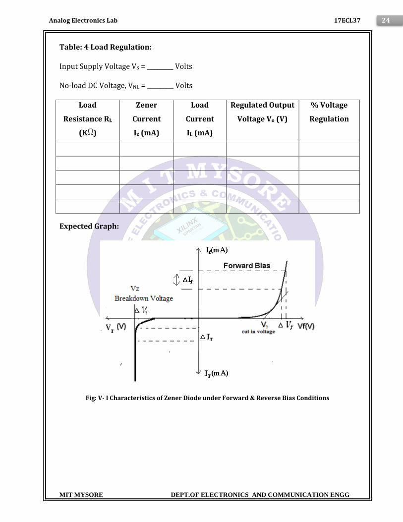
Table: 4 Load Regulation:
Input Supply Voltage VS = _________ Volts
No-load DC Voltage, VNL = _________ Volts
Load
Resistance RL
(K )
Zener
Current
Iz (mA)
Load
Current
IL (mA)
Regulated Output
Voltage Vo (V)
% Voltage
Regulation
Expected Graph:
Fig: V- I Characteristics of Zener Diode under Forward & Reverse Bias Conditions

MIT MYSORE DEPT.OF ELECTRONICS AND COMMUNICATION ENGG
25 Analog Electronics Lab 17ECL37
Line Regulation
Load Regulation:
Calculations from Graph:
Static forward Resistance Rdc = Vf / If
Dynamic Forward Resistance rac = Vf / If
Static Reverse Resistance Rdc = Vr / Ir
Dynamic Reverse Resistance rac = Vr / Ir
For Load regulation,% Voltage Regulation = %
Precautions:
1. While doing the experiment do not exceed the readings of the diode. This may
lead to damaging of the diode.

MIT MYSORE DEPT.OF ELECTRONICS AND COMMUNICATION ENGG
26 Analog Electronics Lab 17ECL37
2. Connect voltmeter and ammeter in correct polarities as shown in the circuit
diagram.
3. Do not switch ON the power supply unless you have checked the circuit
connections as per the circuit diagram.
Result: The characteristics and Voltage Regulation of Zener diode are studied.
a) Forward Bias Zener Diode:
1. The Knee voltage or Cut-in Voltage (Vy) is __________________ Volts.
2. The Dynamic Forward resistance is __________________ .
3. The Static Forward resistance is __________________ .
b) Reverse Bias of Zener Diode:
1. Zener Breakdown Voltage (VZ) is ____________________ Volts.
2. The Dynamic Reverse resistance is __________________ .
3. The Static Reverse resistance is __________________ .
Outcomes: Students are able to
1. Analyze the forward and reverse bias characteristics of Zener diode.
2. Calculate static and dynamic resistance in both forward and reverse bias
condition.
3. Analyze the working of Zener diode as a voltage regulator for line regulation and
load regulation.
Viva Questions:
1. What is the difference between p-n Junction diode and Zener diode?
2. What is break down voltage?
3. What are the applications of Zener diode?
4. What is cut-in-voltage?

MIT MYSORE DEPT.OF ELECTRONICS AND COMMUNICATION ENGG
27 Analog Electronics Lab 17ECL37
5. What is voltage regulator?
6. What is the doping concentration in Zener diodes?
7. Can we use Zener diode as a switch?
8. What is PIV of Zener?
9. What will happen if P-N regions are heavily doped in Zener diode?
10. List the other Zener diodes with different breakdown voltages.
11. Is the breakdown region in Zener really destructible?
12. What is a Zener diode?
13. How the name of the Zener came?
14. What is cause of reverse breakdown?
15. What is Zener voltage?
16. Write the Symbol for the Zener diode.
17. What are the differences between the PN junction diode and Zener diode
fabrication?
18. What are the applications of Zener diode?
19. What are the different types of breakdowns in semiconductor junctions?
20. Compare Zener Breakdown and Avalanche breakdown?
21. What is the max value of voltage of Zener breakdown devices?
22. Zener diode is generally used in ________ biased condition. When Zener diode is
forward biased, it acts as a _________.

MIT MYSORE DEPT.OF ELECTRONICS AND COMMUNICATION ENGG
28 Analog Electronics Lab 17ECL37

MIT MYSORE DEPT.OF ELECTRONICS AND COMMUNICATION ENGG
29 Analog Electronics Lab 17ECL37
EXPERIMENT-04
BJT DARLINGTON EMITTER FOLLOWER
AIM: To determine experimentally and
a) To plot the frequency response of Darlington Emitter Follower and
b) To measure Zi , Zo and find the Current gain Ai.
Equipment and components required:
SL.NO NAME OF EQUIPMENTS/ COMPONENTS SPECIFICATIONS QTY
1. Power Supply 0 – 30 V / 2 Amp D.C. 01
2. A.C.milli Voltmeter(or Digital
Multimeter)
01
3. Function Generator 0 – 3 MHz, 0 – 20 V(p-p) 01
4. CRO Analog, 30 MHz, Dual
Channel
01
5. Terminal Board -- 01
6. Capacitors 0.47 µF (Ceramic) 02
7. DRB -- 02
8. Resistors Designed values
9. Transistor SL 100 02
10. Patch cords, Connecting Wires, etc.
THEORY: Refer Text Book Electronic Devices And Circuit Theory By Robert L.
Boylestad / Louis Nashelsky “ chapter 5“
Procedure:
A] To find Q point:
1) Connect the circuit as shown in the Fig. No. (2)
2) Switch on the power supply and set +12V D.C. as VCC.
3) Measure the DC Voltage using CRO or DC Voltmeter at the VB2, Collector VC2 and
emitter VE2 with respect to Ground.

MIT MYSORE DEPT.OF ELECTRONICS AND COMMUNICATION ENGG
30 Analog Electronics Lab 17ECL37
Then VCE2 = VC2 – VE2
IC2 = IE2 = VE2 / RE
So Q point = (VCE2, IC2)
B] To find Frequency response:
1) Connect the circuit as shown in Fig. No. (1), set VCC = 12 V d.c.
2) Apply a sine wave of 1 V peak to peak amplitude (Vi = 1V p-p) from the Function
Generator.
3) Vary the input sine wave frequency from 10 Hz to 1 MHz in suitable steps and
measure the output Vo of Darlington Emitter Follower circuit at each step using CRO or
AC mili voltmeter (The input Vi must remain constant through the Frequency range).
4) Note down the reading in table given and plot the graph of frequency v/s. Gain in
dB.
BJT Darlington Emitter Follower
Fig. No (1) Circuit Diagram of BJT Darlington Emitter Follower

MIT MYSORE DEPT.OF ELECTRONICS AND COMMUNICATION ENGG
31 Analog Electronics Lab 17ECL37
Fig. No (2) Biasing Circuit BJT Darlington Emitter Follower
Tabular column:
Vin = 1V (p-p)
SL
NO
FREQUENCY
in Hz
Vo(p-p)
in Volts
Av=Vo/Vi POWER GAIN
in dB= 20log10 Av
Fig. (3) Circuit Diagram of BJT Darlington Emitter Follower with Bootstrap

MIT MYSORE DEPT.OF ELECTRONICS AND COMMUNICATION ENGG
32 Analog Electronics Lab 17ECL37
Design:
Let VCC = 12 V D.C. IC2 = 4 mA, β = 100 (for SL 100)
Chose VE2 = VCC / 2 = 12/2 = 6V
RE = 6 / 4mA = 1500 Ω
VB1 = VBE1 + VBE2 + VC2
= 0.7+0.7+6
= 7.4 V
We know 21
21
RR
RVV CCB
21
2
12
4.7
RR
R
21
2616.0RR
R
R2 = 0.616R1 + 0.616R2
0.383R2 = 0.616R1
R2 = 1.61R1
Let R2 = 100 KΩ
R1 = 62.11
Choose R1 = 68 KΩ
(Nearest standard Resistance value)
Choose CC1 = CC2 = 0.47 μF
Current gain [ai]: Vo / Zo Vo Zi
[Ai] Io/Ii = ------------- = ---------. ---------
Vi / Zin Vi Zo
RE = 1.5KΩ

MIT MYSORE DEPT.OF ELECTRONICS AND COMMUNICATION ENGG
33 Analog Electronics Lab 17ECL37
Since Vo = Vin , Ai = Zin / Zo
Procedure:
C] To measure Zi:
1) Connect the circuit as shown in Fig. No (5).
2) Set the following
DRB to minimum (0 Ω)
I/P sine wave amplitude to 1V (p-p)
I/P sine wave frequency to 10 KHz
3) Measure Vo (p-p). Let Vo = Va (say)
4) Increase DRB till Vo = Va/2. The corresponding DRB value gives Zi.
D] To measure Zo:
1) Connect the circuit as shown in Fig. No (6).
2) Set the following
DRB to its maximum resistance value
I/P sine wave amplitude to 1V (p-p)
I/P sine wave frequency to 10 KHz
3) Measure Vo (p-p), let Vo = Vb (say)
4) Decrease DRB till Vo = Vb/2. The corresponding DRB value gives Zo.
E] To measure Zi with bootstrap:
1) Connect the bootstrap circuit as shown in Fig No. (3).
2) Measure Zi as given in [C].

MIT MYSORE DEPT.OF ELECTRONICS AND COMMUNICATION ENGG
34 Analog Electronics Lab 17ECL37
To measure zi:
Fig. No (5)
To measure zo:
Fig. No (6)
Result:
1] Q Point : ________________________
2] Bandwidth (Bw) : ________________________
3] CURRENT GAIN [Ai] : ________________________
4] Input Impedance (Zi without Bootstrap) : ________________________
5] Output Impedance (Z0): ________________________
6] Input Impedance (Zi with Bootstrap): _________________________
Probable viva questions:
1) What are the important characteristics of Darlington emitter follower
2) What are the applications of the Darlington Emitter follower
3) Write the expressions for Av, AI, Vo for the Darlington Emitter follower
4) Explain Bootstrapping technique.

MIT MYSORE DEPT.OF ELECTRONICS AND COMMUNICATION ENGG
35 Analog Electronics Lab 17ECL37
5) Write small signal ac model for the Darlington emitter follower circuit.

MIT MYSORE DEPT.OF ELECTRONICS AND COMMUNICATION ENGG
36 Analog Electronics Lab 17ECL37

MIT MYSORE DEPT.OF ELECTRONICS AND COMMUNICATION ENGG
37 Analog Electronics Lab 17ECL37
EXPERIMENT-05
COMMON EMITTER AMPLIFIER (VOLTAGE DIVIDER BIAS)
AIM: To study the frequency response of Common Emitter Amplifier and calculate its
Bandwidth.
Components Required:
S.No. Name Quantity
1 Transistor BC107 1(One) No.
2 Resistors (100K%u2126, 10K%u2126,
1K%u2126)
1(One) No.
Each
3 Resistors (2.2 K%u2126) 2(Two) No.
4 Capacitors (10µF) 2(Two) No.
5 Capacitors (100µF) 1(One) No.
6 Bread board 1(One) No.
Equipment:
S.No. Name Quantity
1 Dual DC Regulated Power supply (0 – 30 V) 1(One) No.
2 Cathode Ray Oscilloscope (CRO) (0-20MHz) 1(One) No.
3 Function Generator (0-1MHz) 1(One) No.
4 Connecting wires (Single Strand)
Theory:
The common emitter configuration is widely used as a basic amplifier as it has
both voltage and current amplification. Resistors R1 and R2 form a voltage divider
across the base of the transistor. The function of this network is to provide necessary
bias condition and ensure that emitter-base junction is operating in the proper region.
In order to operate transistor as an amplifier, biasing is done in such a way that
the operating point is in the active region. For an amplifier the Q-point is placed so that
the load line is bisected. Therefore, in practical design VCE is always set to VCC/2. This
will confirm that the Q-point always swings within the active region. This limitation can

MIT MYSORE DEPT.OF ELECTRONICS AND COMMUNICATION ENGG
38 Analog Electronics Lab 17ECL37
be explained by maximum signal handling capacity. For the maximum input signal,
output is produced without any distortion and clipping.
The Bypass Capacitor:
The emitter resistor RE is required to obtain the DC quiescent point stability.
However the inclusion of RE in the circuit causes a decrease in amplification at higher
frequencies. In order to avoid such a condition, it is bypassed by a capacitor so that it
acts as a short circuit for AC and contributes stability for DC quiescent condition. Hence
capacitor is connected in parallel with emitter resistance.
The Input/ Output Coupling (or Blocking) Capacitor: An amplifier amplifies
the given AC signal. In order to have noiseless transmission of a signal (without DC), it
is necessary to block DC i.e. the direct current should not enter the amplifier or load.
This is usually accomplished by inserting a coupling capacitor between two stages.
XCC << ( Ri hie )
CC - Output Coupling Capacitor
CB - Input Coupling Capacitor
Frequency response of Common Emitter Amplifier:
Emitter bypass capacitors are used to short circuit the emitter resistor and thus
increases the gain at high frequency. The coupling and bypass capacitors cause the fall
of the signal in the low frequency response of the amplifier because their impedance
becomes large at low frequencies. The stray capacitances are effectively open circuits.

MIT MYSORE DEPT.OF ELECTRONICS AND COMMUNICATION ENGG
39 Analog Electronics Lab 17ECL37
In the mid frequency range large capacitors are effectively short circuits and the stray
capacitors are open circuits, so that no capacitance appears in the mid frequency range.
Hence the mid band frequency gain is maximum.
At the high frequencies, the bypass and coupling capacitors are replaced by short
circuits. The stray capacitors and the transistor determine the response.
Characteristics of CE Amplifier:
1. Large current gain.
2. Large voltage gain.
3. Large power gain.
4. Current and voltage phase shift of 1800.
5. Moderated output resistance.
Circuit Diagram:

MIT MYSORE DEPT.OF ELECTRONICS AND COMMUNICATION ENGG
40 Analog Electronics Lab 17ECL37
Procedure:
1. Connect the circuit as shown in the circuit diagram.
2. Set source voltage VS = 50mV (say) at 1 KHz frequency using the function
generator. Observe the phase difference between input and output by giving
these two signals to the dual channels of CRO.
3. Keeping input voltage constant, vary the frequency from 50 Hz to 1 MHz in
regular steps and note down the corresponding output voltage. Calculate gain in
dB as shown in the tabular column.
4. Plot the graph: gain (dB) verses Frequency on a semi log graph sheet.
5. Calculate the 3-dB bandwidth from the frequency response.
Expected waveform:
(a) The Input & Output Waveforms at 1 KHz
(b) Frequency Response Curve
In the usual application, mid band frequency range are defined as those frequencies at
which the response has fallen to 3dB below the maximum gain (|A| max). These are
shown as fL and fH and are called as the 3dB frequencies (Lower and Upper Cut-Off
Frequencies respectively). The difference between higher cut-off and lower cut-off
frequency is referred to as bandwidth (fH - fL).

MIT MYSORE DEPT.OF ELECTRONICS AND COMMUNICATION ENGG
41 Analog Electronics Lab 17ECL37
Fig: Frequency Response Curve
Calculations from the graph
Bandwidth = fH – fL (in Hz)
Observation tables:
VS = 50mV
Frequency Vo(Volts) Gain = Vo/Vs Gain(dB) = 20 log(Vo/Vs)
Result:
Common Emitter Amplifier is studied and its Bandwidth is calculated.
1. Maximum Gain ( Amax ) = ___________ dB
2. 3dB Gain = ___________ dB
3. 3dB Lower cut-off frequency, fL = ___________ Hz
4. 3dB Upper cut-off frequency, fH = ___________ Hz

MIT MYSORE DEPT.OF ELECTRONICS AND COMMUNICATION ENGG
42 Analog Electronics Lab 17ECL37
5. 3dB Bandwidth ( fH - fL ) = ___________ Hz
Outcomes: Students are able to
1. Calculate the Bandwidth of BJT Common Emitter amplifier.
Viva Questions:
1. What is the equation for voltage gain?
Ans:
2. What is cut off frequency? What is lower 3dB and upper 3dB cut off frequency?
3. What are the applications of CE amplifier?
4. What is active region?
5. What is Bandwidth of an amplifier?
6. What is the importance of gain bandwidth product?
7. Draw h parameter equivalent circuit of CE amplifier.
8. What is the importance of coupling capacitors in CE amplifier?
9. What is the importance of emitter by pass capacitor?
10. What type of feedback is used in CE amplifier?
11. What are the various types of biasing a Transistor?
12. What is Q point of operation of the transistor? What is the region of operation of the
transistor when it is working as an amplifier?
13. Why frequency response of the amplifier is drawn on semi-log scale graph?
14. If Q point is not properly selected, then what will be the effect on the output
waveform?
15. What are the typical values of the input impedance and output impendence of CE
amplifier?

MIT MYSORE DEPT.OF ELECTRONICS AND COMMUNICATION ENGG
43 Analog Electronics Lab 17ECL37
EXPERIMENT-06
CHARACTERISTICS OF JFET
AIM: To study Drain Characteristics and Transfer Characteristics of a Field Effect
Transistor (FET).
Components:
S.No. Name Quantity
1 JFET (BFW11/ BFW10) 1(One) No.
2 Resistor (1K ,100K ) 1(One) No. Each
3 Bread board 1(One) No.
Equipment:
S.No. Name Quantity
1 Dual DC Regulated Power supply (0 - 30 V) 1(One) No.
2 Digital Ammeters ( 0 - 200 mA) 1(One) No.
3 Digital Voltmeter (0 - 20V) 2(Two) No.
4 Connecting wires (Single Strand)
Specifications:
For FET BFW11:
Gate Source Voltage VGS = -30V
Forward Gain Current IGF = 10mA
Maximum Power Dissipation PD = 300mW

MIT MYSORE DEPT.OF ELECTRONICS AND COMMUNICATION ENGG
44 Analog Electronics Lab 17ECL37
Circuit Diagram:
Figure 1.
Pin assignment of FET:
Top View
Bottom View

MIT MYSORE DEPT.OF ELECTRONICS AND COMMUNICATION ENGG
45 Analog Electronics Lab 17ECL37
Operation:
The circuit diagram for studying drain and transfer characteristics is shown in the
figure1.
1. Drain characteristics are obtained between the drain to source voltage (VDS) and
drain current (ID) taking gate to source voltage (VGS) as the constant parameter.
2. Transfer characteristics are obtained between the gate to source voltage (VGS)
and drain current (ID) taking drain to source voltage (VDS) as the constant
parameter.
Procedure:
Drain Characteristics:
1. Connect the circuit as shown in the figure1.
2. Keep VGS = 0V by varying VGG.
3. Varying VDD gradually in steps of 1V up to 10V note down drain current ID and
drain to source voltage (VDS).
4. Repeat above procedure for VGS = -1V.
Transfer Characteristics:
1. Connect the circuit as shown in the figure1.
2. Set voltage VDS = 2V/5V (BFW10/ BFW11).
3. Varying VDD in steps of 0.5V until the current ID reduces to minimum value.
4. Varying VGG gradually, note down both drain current ID and gate-source voltage
(VGS).
5. Repeat above procedure (step 3) for VDS = 4V/ 8V (BFW10/ BFW11).

MIT MYSORE DEPT.OF ELECTRONICS AND COMMUNICATION ENGG
46 Analog Electronics Lab 17ECL37
Observations:
Drain Characteristics
VDD (Volts) VGS = 0V VGS = -1V
VDS(Volts) ID(mA) VDS(Volts) ID(mA)
Transfer Characteristics
VGG (Volts) VDS = 2V/5V VDS = 4V/8V
VGS(Volts) ID(mA) VGS(Volts) ID(mA)
Graph:
1. Plot the drain characteristics by taking VDS on X-axis and ID on Y-axis at a
constant VGS.
2. Plot the transfer characteristics by taking VGS on X-axis and taking ID on Y-axis at
constant VDS.

MIT MYSORE DEPT.OF ELECTRONICS AND COMMUNICATION ENGG
47 Analog Electronics Lab 17ECL37
Calculations from Graph:
1. Drain Resistance (rd): It is given by the relation of small change in drain to
source voltage ( VDS) to the corresponding change in Drain Current ( ID) for a
constant gate to source voltage ( VGS), when the JFET is operating in pinch-off
region.
at a constant VGS (from drain characteristics)
2. Trans Conductance (gm): Ratio of small change in drain current ( ID) to the
corresponding change in gate to source voltage ( VGS) for a constant VDS.
gm at constant VDS (from transfer characteristics).
The value of gm is expressed in mho’s ( ) or Siemens (s).
3. Amplification factor (µ): It is given by the ratio of small change in drain to
source voltage ( VDS) to the corresponding change in gate to source voltage (
VGS) for a constant drain current (ID).
Inference:
1. As the gate to source voltage (VGS) is increased above zero, pinch off voltage is
increased at a smaller value of drain current as compared to that when VGS = 0V.
2. The value of drain to source voltage (VDS) is decreased as compared to that when
VGS = 0V.
Precautions:
1. While performing the experiment do not exceed the ratings of the FET. This may
lead to damage of FET.
2. Connect voltmeter and ammeter with correct polarities as shown in the circuit
diagram.

MIT MYSORE DEPT.OF ELECTRONICS AND COMMUNICATION ENGG
48 Analog Electronics Lab 17ECL37
3. Do not switch ON the power supply unless the circuit connections are checked as
per the circuit diagram.
4. Properly identify the Source, Drain and Gate terminals of the transistor.
Result:
Outcomes: Students are able to
1. Analyze the Drain and transfer characteristics of FET in Common Source
configuration.
2. Calculate the parameters Trans conductance (gm), drain resistance (rd) and
amplification factor (µ).
Viva Questions:
1. Why FET is called a unipolar device?
2. What are the advantages of FET?
3. What is trans conductance?
4. What are the disadvantages of FET?
5. Relation between µ, gm and rd?
6. Why an input characteristic of FET is not drawn?
7. What is the importance of high input impedance?
8. Why wedge shaped depletion region is formed in FET under reverse bias gate
condition?
9. Why FET is less noisy?
10. What is the difference between n- channel FET and p-channel FET?

MIT MYSORE DEPT.OF ELECTRONICS AND COMMUNICATION ENGG
49 Analog Electronics Lab 17ECL37

MIT MYSORE DEPT.OF ELECTRONICS AND COMMUNICATION ENGG
50 Analog Electronics Lab 17ECL37

MIT MYSORE DEPT.OF ELECTRONICS AND COMMUNICATION ENGG
51 Analog Electronics Lab 17ECL37
EXPERIMENT-07
FREQUENCY RESPONSE OF COMMON SOURCE JFET AMPLIFIER
AIM: To study the JFET common source amplifier and find it’s cut off frequencies and
Bandwidth.
Components:
Name Quantity
JFET BFW 11 1
Resistor 6.8K , 8.2K , 1M 2, 1, 1
Capacitor 10µF, 100µF 2,1
Equipment:
Name Range Quantity
Bread Board 1
Dual power supply 0-30V 1
CRO (0-20)MHz 1
Function Generator (0-1)MHz 1
Connecting Wires
Theory:
Of the possible three configurations of JFET amplifiers, common source (CS)
configuration is mostly used. The advantage of using CS configuration is that it has very
high input impedance. Circuit diagram shows the FET amplifier of common source
configuration. The biasing input and couplings are shown in the figure. The mid-range
voltage gain of the amplifier is given by A = gm(rd || RL) At the mid-frequency range,
there is n effect of input and output coupling capacitors. Therefore, the voltage gain and
phase angle are constant in this frequency range. The amplifier shown in the circuit
diagram has only two RC networks that influence its low-frequency response. One
network is formed by the output coupling capacitors and the output impedance looking
at the drain. Just as in the case of BJT amplifier, the reactance of the input coupling

MIT MYSORE DEPT.OF ELECTRONICS AND COMMUNICATION ENGG
52 Analog Electronics Lab 17ECL37
capacitor, reactance increases as the frequency decreases. The phase angle also changes
with change in frequency.
As the frequency is increased beyond mid-frequency range the internal
transistor capacitance effect is predominant. For JFET’s is the internal capacitance
between gate and source. This is also called input capacitance,. The other internal
capacitance, which effects the performance it acts as a feedback circuit, which couples
both, input and output. The effect of both these capacitances is that it reduced the gain
appreciably as in the case of BJT.
Circuit Diagram:
Procedure:
1. Connect the circuit as shown in the circuit diagram.
2. Set source voltage VS = 50mV (say) at 1 KHz frequency using the function
generator.
3. Keeping input voltage constant vary the frequency from 50 Hz to 1 MHz in
regular steps and note down the corresponding output voltage.
4. Plot the graph: gain (dB) verses Frequency on a semi log graph sheet.

MIT MYSORE DEPT.OF ELECTRONICS AND COMMUNICATION ENGG
53 Analog Electronics Lab 17ECL37
5. Calculate the bandwidth from the graph.
6. Calculate all the parameters at mid band frequencies (i.e. at 1 KHz).
7. To calculate voltage gain
Gain AVS = Output Voltage (VO) / Source Voltage (VS)
Expected waveform:
In the usual application, mid band frequency range are defined as those
frequencies at which the response has fallen to 3dB below the maximum gain (|A| max).
These are shown as fL and fH and are called as the 3dB frequencies are simply the lower
and higher cut off frequencies respectively. The difference between higher cut off and
lower cut off frequency is referred to as bandwidth (fH - fL).
Observation tables:
VS = 50mV
Frequency Vo(volts) Gain= Vo/Vs Gain(dB)=20 log(Vo/Vs)

MIT MYSORE DEPT.OF ELECTRONICS AND COMMUNICATION ENGG
54 Analog Electronics Lab 17ECL37
Result:
Viva Questions:
1. Why FET is called as unipolar device?
2. Why the common-source (CS) amplifier may be viewed as a transconductance
amplifier or as a voltage amplifier?
3. What are the characteristics of JFET source amplifier?
4. What is the impedance of FET?

MIT MYSORE DEPT.OF ELECTRONICS AND COMMUNICATION ENGG
55 Analog Electronics Lab 17ECL37

MIT MYSORE DEPT.OF ELECTRONICS AND COMMUNICATION ENGG
56 Analog Electronics Lab 17ECL37

MIT MYSORE DEPT.OF ELECTRONICS AND COMMUNICATION ENGG
57 Analog Electronics Lab 17ECL37
EXPERIMENT-08
INPUT AND OUTPUT CHARACTERISTICS OF N-CHANNEL MOSFET
AIM: To plot the transfer and drain characteristics of n-channel MOSFET and to find the
following parameters
1. Drain resistance
2. Mutual conductance
3. Amplification factor
Components Required:
SL. no EQUIPMENT RANGE
1. Power supply (0-30)V
2. Ammeter (0-100)mA
3. Voltmeter (0-30)V
4. Bread board & wires -
5. Transistor BFW 96
THEORY
MOSFETs are three terminal devices having a source, gate and drain. MOSFET is
the abbreviation of metal oxide semiconductor field effect transistor. It uses a thin layer
of silicon dioxide as an insulator between gate and channel. It is also known as
insulated gate field effect transistor (IGFET). There are two kinds of MOSFET,
depletion and enhancement type.
An N-channel depletion type MOSFET is shown in figure. A heavily doped two N-
type wells are doped on P-type substrate to form source and drain. Between these two
N-type wells a lightly doped N-type material forms a channel. A thin layer of Sio2 which
is an insulating material is fabricated on the surface above the channel and gate

MIT MYSORE DEPT.OF ELECTRONICS AND COMMUNICATION ENGG
58 Analog Electronics Lab 17ECL37
terminal is attached to it. Source and drain terminals are attached to heavily doped N-
type material with metal contacts.
A positive voltage VDS is applied at the drain with respect to source to establish
drain current. When a negative voltage VGS is applied at the gate with respect to the
source, electrons under gate get repelled causing the channel effectively thinner. This
reduces the current through the channel. If the magnitude of VGS is increased, the drain
current decreases. If it is increased further drain current stops.
If a positive voltage is applied at the gate, electrons get attracted in to the
channel and drain current increases. A depletion type MOSFET can operate in depletion
and enhancement modes.
Application
MOSFETs are widely used in VLSI circuits.
Symbol and Pin Diagram

MIT MYSORE DEPT.OF ELECTRONICS AND COMMUNICATION ENGG
59 Analog Electronics Lab 17ECL37
Circuit Diagram:
Drain Resistance
It is defined as the ratio of change in drain to source voltage to the change in drain
current at an operating point, when gate to source voltage remains constant.
Rd = ΔVDS / ΔID with VGS constant
Mutual Conductance
It is defined as the ratio of change in drain current to the change in gate to source
voltage at an operating point, when drain to source voltage remains constant.
Gm = ΔID / ΔVGS with VDS constant.
Amplification Factor
It is defined as the product of drain resistance and mutual conductance.
μ = Rd * Gm

MIT MYSORE DEPT.OF ELECTRONICS AND COMMUNICATION ENGG
60 Analog Electronics Lab 17ECL37
Procedure:
Drain Characteristics
1. Rig up the circuit as per circuit diagram.
2. Set VGS = 0V and vary VDS insteps of 0.5 V and note down the corresponding ID.
Repeat the above procedure for VGS = -1V,-2V,-3V , for the depletion mode
3. Repeat the above procedure for VGS = 1V, 2V, 3V, for the enhancement mode.
4. Plot the graph: VDS vs ID for constant values of VGS.
5. Find the drain resistance Rd = ΔVDS / ΔID with VGS constant
Transfer Characteristics
1. Rig up the circuit as per circuit diagram.
2. Set VDS and vary VGS insteps of 0.5 V and note down the corresponding ID. Repeat
the above procedure for various values of VDS.
3. Plot the graph: VGS vs ID for constant values of VDS.
4. Find the Trans conductance. Gm = ΔID / ΔVGS with VDS constant.

MIT MYSORE DEPT.OF ELECTRONICS AND COMMUNICATION ENGG
61 Analog Electronics Lab 17ECL37
Tabulation
Drain characteristics – Depletion mode
SL. No VGS = VGS = VGS =
VDS (V) ID (mA) VDS (V) ID (mA) VDS (V) ID (mA)
1.
2.
3.
4.
5.
6.
7.
8.
Drain characteristics – Depletion mode
SL. No VGS = VGS = VGS =
VDS (V) ID (mA) VDS (V) ID (mA) VDS (V) ID (mA)
1.
2.
3.
4.
5.
6.
7.

MIT MYSORE DEPT.OF ELECTRONICS AND COMMUNICATION ENGG
62 Analog Electronics Lab 17ECL37
Transfer characteristics
VDS = _________
SL. No. VGS (V) ID (mA)
1.
2.
3.
4.
5.
Calculation
Drain resistance Rd = ΔVDS / ΔID
=
Mutual conductance Gm = ΔID / ΔVGS
=
Amplification factor μ = Rd * Gm
=

MIT MYSORE DEPT.OF ELECTRONICS AND COMMUNICATION ENGG
63 Analog Electronics Lab 17ECL37
Model graph
Drain characteristics Transfer Characteristics:
RESULT:
Drain resistance Rd
Mutual conductance
Gm
Amplification factor μ
VIVA-VOCE QUESTIONS
1. What is a unipolar device?
2. What are the types of FET?
3. How a MOSFET is formed?
4. Mention the modes of MOSFET.
5. Explain enhancement mode.

MIT MYSORE DEPT.OF ELECTRONICS AND COMMUNICATION ENGG
64 Analog Electronics Lab 17ECL37
EXPERIMENT NO-09
TESTING OF A TRANSFORMERLESS CLASS B PUSH PULL POWER AMPLIFIER
AND DETERMINATION OF ITS CONVERSION EFFICIENCY
AIM: To determine conversion efficiency of a transformer less class B push pull
Amplifier.
Equipment and components required:
SL.NO NAME OF EQUIPMENTS/
COMPONENTS
SPECIFICATIONS QTY
1. Power supply 0-30V/2AMP D.C. 01
2. Function Generator 0-3MHz,0-20VP-P 01
3. CRO 01
4. Transistors SL100,SK100 01
5. Resistors Designed value 01
6. Terminal board 01
7. C R O 01
8. Patch cords, Connecting Wires, etc.
Circuit Diagram:
Fig: Transformer less class B push pull power amplifier
E
RL 470Ω
B
E
C
B
C
Vi (0-20VPP)
C 0.33µF
T1
SL1000
T2
SK100
VCC1
10V
VCC2
10V

MIT MYSORE DEPT.OF ELECTRONICS AND COMMUNICATION ENGG
65 Analog Electronics Lab 17ECL37
Procedure:
1. Rig up the circuit as shown in the figure.
2. Adjust VCC to 10V each.
3. Vary the input signal voltage from 0V to 20VPP and observe the output voltage
(peak) using CRO across load resistor (RL) in AC mode.
4. Calculate the efficiency.
Design:
Assume RL=470Ω such that the collector current is less than the maximum collector
current of transistor. Then
ICmax=10/470 = 21.2mA (≤ICmax of transistor)
PDmax (across the transistor) = Pi (dc) max – PO (ac)
=135mW-0
=135mW (≤ PDmax of transistor)
Let output load voltage= V0 (P)
Then IC (P) =V0 (P)/RL
Idc=2IC (P)/∏
Therefore Pi (dc) =Vcc x Idc
P0 (ac) = V0 (P) 2/2RL
Pi (dc) max = VCC X Idc (max)
= 10.2(10)/ (∏) (470Ω)
Pi (dc) max=135mW

MIT MYSORE DEPT.OF ELECTRONICS AND COMMUNICATION ENGG
66 Analog Electronics Lab 17ECL37
Tabular column
Sl
no
Vin(pp)
(V)
V0(P)
(V)
Idc
(mA)
Pi(dc)
(mW)
P0(ac)
(mW)
Efficiency
η%
NOTE: Maximum efficiency is obtained when V0 (P) =VCC
Result:
Output waveform
T
VO
0
MIT MYSORE DEPT.OF ELECTRONICS AND COMMUNICATION ENGG
67 Analog Electronics Lab 17ECL37
Viva questions:
1) What do you understand by Operating point?
2) Why do we choose the Q point at the center of the load line?
3) Name the two techniques used in the stability of the q point .explain.?
4) Define stability factor &Give the expression for stability factor?
5) List out the different types of biasing.
6) What do you meant by thermal runway?
7) Why transistor is called as a current controlled device?
8) Define current amplification factor?
9) What are the requirements for biasing circuits?
10) When does a transistor act as a switch?
11) What is biasing?
12) What is an operating point?
13) What is d.c load line?
14) Explain about the various regions in a transistor?
15) Explain about the characteristics of a transistor?
16) Why the operating point is selected at the Centre of the active region?
17) What is an amplifier?
18) What is small signal amplifier?
19) What is a Darlington pair?

MIT MYSORE DEPT.OF ELECTRONICS AND COMMUNICATION ENGG
68 Analog Electronics Lab 17ECL37

MIT MYSORE DEPT.OF ELECTRONICS AND COMMUNICATION ENGG
69 Analog Electronics Lab 17ECL37

MIT MYSORE DEPT.OF ELECTRONICS AND COMMUNICATION ENGG
70 Analog Electronics Lab 17ECL37
EXPERIMENT NO-10
RC PHASE SHIFT OSCILLATOR
AIM: To design and test a RC Phase Shift Oscillator for a given frequency
Equipment and components required:
SL
NO
NAME OF EQUIPMENTS/ COMPONENTS SPECIFICATIONS QTY.
1. Power Supply 0 – 30 V / 2 Amp D.C. 01
2. CRO Analog, 30MHz, Dual Channel 01
3. Terminal Board -- 01
4. Capacitors 0.01 µF
0.47 µF
03
01
5. Potentiometer 10 KΩ 01
6. Resistors Designed values
7. Transistor BC107 01
8. Patch cords, Connecting Wires,etc. 01
THEORY: Refer Text Book Electronic Devices And Circuit Theory By Robert L.
Boylestad / Louis Nashelsky “chapter 14” page No 746
Circuit Diagram:
Fig. (1) Circuit Diagram of R C Phase Shift Oscillator

MIT MYSORE DEPT.OF ELECTRONICS AND COMMUNICATION ENGG
71 Analog Electronics Lab 17ECL37
Fig. (2) Circuit Diagram of R C Phase Shift Oscillator using FET
DESIGN:
Let VCC = 12 volts IC = 3mA, β = 100(for SL 100)
Choose VE = VCC / 10 = 12/10 = 1.2 V
VE = IERE = 1.2 V
RE = 1.2/Ic = 1.2/3mA = 0.400 KΩ (IE ≈ IC)
RC: Choose VCE = VCC /2 12/2 = 6V
Apply KVL in CE loop:
VCC – ICRC – VCE – VRE = 0
12 – 3mRc – 6 – 1.2 = 0
RC = 1.6 KΩ
Select
R1 and R2:
VB = VBE + VE = 0.7 +470* 3mA = 2.11 V
I2 ≈ IC/10 = .3mA
Then R2=Vb/.3mA =7.03KΩ
RE = 470 Ω
RC = 1KΩ

MIT MYSORE DEPT.OF ELECTRONICS AND COMMUNICATION ENGG
72 Analog Electronics Lab 17ECL37
Let us assume R2 = 6.8KΩ
R1=vcc-vb/I1 (I1=I2) = ( 12-2.11)/.3mA
R1 = 32.9KΩ
Choose R1 = 33KΩ
Procedure:
1] Connect the circuit as shown in Fig. (1).
2] Switch on the D.C. power supply.
3] Observe the output Vo on CRO. The 10 K pot is adjusted to get a stable output on the
CRO.
4] Measure the frequency of the output wave.
5] Compare the measured frequency with theoretical value.
6] With respect to output at point P, observe the waveforms at point Q, R and S on the
CRO. We can see that phase shift at each point being 60°, 120° and 180° respectively.
7] repeat the design for different value of frequency (in Audio range only). At each
case
Compare the generated frequency with theoretical value.
Note:
a) the last Resistor in the phase shifting network is chosen to be a 10 K pot. This is done
to get a overall phase shift of 180° at frequency of Oscillations.
b) The minimum hfe required for the transistor to oscillate is
Hfemin = 23 + 29(R / RC) + 4(RC / R)
Where RC = 1 KΩ and R = 2.2 KΩ (Phase Shifting Network)
Hfe min = 23 + 29(2.2K / 1K) + 4 = 1K / 2.2K
≈ 89
The transistor should be chosen to have a value of hfe greater than 89.
By pass capacitor CE: Let 10
ECE
RX =470/10 =4
At f = 100 Hz; 102
1 ER
fce
Ce=33µF

MIT MYSORE DEPT.OF ELECTRONICS AND COMMUNICATION ENGG
73 Analog Electronics Lab 17ECL37
Choose CE = 47 µF (electrolytic)
Cc1 and CC2: Assume CC1= CC2=0.47 µF (ceramic)
To design:
10
)||(1
RbhieXcc
10
)||2
RLRcXcc
12
11
CcXcc
22
12
CcXcc
CC1 =? CC2 =?
Design of phase shifting network:
The frequency of oscillations is determined by phase shifting network.
The oscillating frequency for the above circuit is given by
R
RcRC
f
462
1
The ratio Rc / R is usually < 1
Let f = 1 KHz (Audio frequency in the range 20 Hz to 20 KHz) and R = 3.9 KΩ
Since Rc = 1KΩ we get
K
KC
9.3
146109.3142.32101
1
33
202.7109.3142.321
16
C
65.2109.3142.321
16
C
6
61001.0
1090.64
1
C
C = 0.01 µF
RESULT: ______________

MIT MYSORE DEPT.OF ELECTRONICS AND COMMUNICATION ENGG
74 Analog Electronics Lab 17ECL37
Probable viva questions:
1) What is Barkhausen’s criterion?
2) How oscillations are generated in RC Phase Shift Oscillator?
3) Give the condition which determines the frequency of oscillation
4) Explain the phase-shift principle in Lc oscillators?
5) Compare and contrast RC & LC oscillators
6) Where do you use IC oscillators?
MIT MYSORE DEPT.OF ELECTRONICS AND COMMUNICATION ENGG
75 Analog Electronics Lab 17ECL37

MIT MYSORE DEPT.OF ELECTRONICS AND COMMUNICATION ENGG
76 Analog Electronics Lab 17ECL37
EXPERIMENT NO-11
HARTLEY OSCILLATOR AND COLPITT’S OSCILLATOR
AIM: To design and test a Hartley and Colpitt’s Oscillator for a given frequency
Equipment and components required:
SL.NO NAME OF EQUIPMENTS/ COMPONENTS SPECIFICATIONS QTY
1. Power Supply 0 – 30 V / 2 Amp D.C. 01
2. A.C.Milli Voltmeter(or Digital Multimeter) 01
3. CRO Analog, 30MHz, Dual
Channel
01
4. Terminal Board -- 01
5. Capacitors 0.47 µF (Ceramic)
47 µF (Electrolytic)
1000pF (or DCB)
02
01
6. Resistors Designed values
7. Inductance 1mH (or DIB)
2.2mH (or DIB)
01
01
8. Transistor SL 100 01
9. Patch cords, Connecting Wires, etc.
THEORY :Refer Text Book Electronic Devices And Circuit Theory By Robert L.
Boylestad / Louis Nashelsky Chapter“14 “ page no 751.
Procedure:
1] Connect the circuit as shown in Fig. (1)
2] Switch on the D.C. power supply.
3] Observe the output on CRO screen.
4] Measure the frequency of the output wave.
5] Compare the measured frequency with theoretical value.
6] Repeat the design for different value of frequency. At each case compare the
generated frequency with theoretical value.
MIT MYSORE DEPT.OF ELECTRONICS AND COMMUNICATION ENGG
77 Analog Electronics Lab 17ECL37
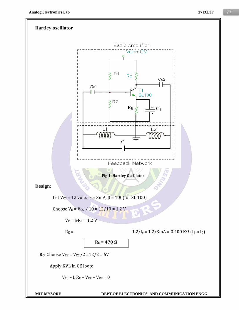
Hartley oscillator
Fig 1: Hartley Oscillator
Design:
Let VCC = 12 volts IC = 3mA, β = 100(for SL 100)
Choose VE = VCC / 10 = 12/10 = 1.2 V
VE = IERE = 1.2 V
RE = 1.2/Ic = 1.2/3mA = 0.400 KΩ (IE ≈ IC)
RC: Choose VCE = VCC /2 =12/2 = 6V
Apply KVL in CE loop:
VCC – ICRC – VCE – VRE = 0
RE = 470 Ω

MIT MYSORE DEPT.OF ELECTRONICS AND COMMUNICATION ENGG
78 Analog Electronics Lab 17ECL37
12 – 3mRc – 6 – 1.2 = 0
RC = 1.6 KΩ
Select
R1 and R2:
VB = VBE + VE = 0.7 +470* 3mA = 2.11 V
I2 ≈ IC/10 = .3mA
Then R2=Vb/.3mA
=7.03KΩ
Let us assume
R1=vcc-vb/I1 (I1=I2)
= ( 12-2.11)/.3mA
R1 = 32.9KΩ
Choose R1 = 33KΩ
By pass capacitor CE:
Let 10
ECE
RX =470/10 =47
At f = 100 Hz; 102
1 ER
fce
Ce=33µF
Choose CE = 47 µF (electrolytic)
Cc1 and CC2: Assume CC1= CC2=0.47 µF (ceramic)
RC = 1KΩ
R2 = 6.8KΩ

MIT MYSORE DEPT.OF ELECTRONICS AND COMMUNICATION ENGG
79 Analog Electronics Lab 17ECL37
To design:
10
)||(1
RbhieXcc
10
)||2
RLRcXcc
12
11
CcXcc
22
12
CcXcc
CC1 =? CC2 =?
Tank Circuit Design:
Oscillator Frequency f = 100 KHz
f = ..2
1
CLeq = 100 x 103 =
..2
1
CLeq
Where Leq. = L1 + L2
In designing Split Inductors, the ratio
21
2 L
L or L2 = 2L1
Let L1 = 1 mH L2 = 2.2 mH Leq = 3.2 mH
D) 22 .4
1
fLC
eq = 791.57 pF
Choose C=1000 pF
RESULT: ______________

MIT MYSORE DEPT.OF ELECTRONICS AND COMMUNICATION ENGG
80 Analog Electronics Lab 17ECL37
Colpitt’s Oscillator:
SL.NO NAME OF EQUIPMENTS/ COMPONENTS SPECIFICATIONS QTY
1. Power Supply 0 – 30 V / 2 Amp D.C. 01
2. A.C.Milli Voltmeter(or Digital Multimeter) 01
3. CRO Analog, 30MHz, Dual
Channel
01
4. Terminal Board -- 01
5. Capacitors 0.47 µF (Ceramic)
47 µF (Electrolytic)
2200pF (or DCB)
1000pF (or DCB)
02
01
01
01
6. Resistors
7. Inductance 3.6mH (or DIB) 01
8. Transistor SL 100 01
9. Patch cords, Connecting Wires,etc.
THEORY: Refer Text Book Electronic Devices And Circuit Theory By Robert L.
Boylestad / Louis Nashelsky Chapter“14“ page no 750.
Procedure:
1] Connect the circuit as shown in Fig. (1).
2] Switch on the D.C. power supply.
3] Observe the output waveform on CRO screen.
4] Measure the frequency of the output waveform.
5] Compare the measured frequency with theoretical value.
6] Repeat the design for different values of frequency. At each case compare the
generated frequency with theoretical value.

MIT MYSORE DEPT.OF ELECTRONICS AND COMMUNICATION ENGG
81 Analog Electronics Lab 17ECL37
Circuit Diagram:
Fig. (1) Circuit Diagram of Colpitt’s Oscillator
Design:
Let VCC = 12 volts IC = 3mA, β = 100(for SL 100)
Choose VE = VCC / 10 = 12/10 = 1.2 V
VE = IERE = 1.2 V
RE = 1.2/Ic = 1.2/3mA = 0.400 KΩ (IE ≈ IC)
RC: Choose VCE = VCC /2 12/2 = 6V
Apply KVL in CE loop:
VCC – ICRC – VCE – VRE = 0
RE = 470 Ω

MIT MYSORE DEPT.OF ELECTRONICS AND COMMUNICATION ENGG
82 Analog Electronics Lab 17ECL37
12 – 3mRc – 6 – 1.2 = 0
RC = 1.6 KΩ
Select
R1 and R2:
VB = VBE + VE = 0.7 +470* 3mA = 2.11 V
I2 ≈ IC/10 = .3mA
Then R2=Vb/.3mA
=7.03KΩ
Let us assume R2 = 6.8KΩ
R1=vcc-vb/I1 (I1=I2)
= ( 12-2.11)/.3mA
R1 = 32.9KΩ
Choose R1 = 33KΩ
By pass capacitor CE:
Let 10
ECE
RX =470/10 =47
At f = 100 Hz; 102
1 ER
fce
Ce=33µF
Choose CE = 47 µF (electrolytic)
Cc1 and CC2: Assume CC1= CC2=0.47 µF (ceramic)
To design:
10
)||(1
RbhieXcc
10
)||2
RLRcXcc
RC = 1KΩ

MIT MYSORE DEPT.OF ELECTRONICS AND COMMUNICATION ENGG
83 Analog Electronics Lab 17ECL37
12
11
CcXcc
22
12
CcXcc
CC1 =? CC2 =?
Tank Circuit Design:
Oscillation frequency f = 100 KHz
eqLC
f2
1
Where 21
21
CC
CCC
Assume C1= 1000 pF and C2 = 2200 pF
12
24
10)22001000(
1022001000
C
pFC 5.687)22001000(
1022001000 12
Cf
L)(4
122
L = 3.6mH
RESULT: _______________

MIT MYSORE DEPT.OF ELECTRONICS AND COMMUNICATION ENGG
84 Analog Electronics Lab 17ECL37
Probable viva questions:
1) what is a tank circuit
2) what are the important components of tank circuit
3) What are the advantages of Hartley oscillator compared to RC-phase shift
oscillator.
4) What is the frequency range of Hartley Oscillator
5) Explain the conditions required to produce sustained oscillations
6) What are the basic properties of an inductor and a capacitor?
7) Explain Barkhausen criteria for sustained oscillations
8) What is the difference between Hartley and colpitts oscillator
9) Explain the condition for sustained oscillations for colpitts oscillator
10) Write the equation for frequency for oscillations and conditions for sustained
oscillations
11) Write the frequency range of colpitts oscillator

MIT MYSORE DEPT.OF ELECTRONICS AND COMMUNICATION ENGG
85 Analog Electronics Lab 17ECL37

MIT MYSORE DEPT.OF ELECTRONICS AND COMMUNICATION ENGG
86 Analog Electronics Lab 17ECL37
EXPERIMENT NO-12
CRYSTAL OSCILLATOR
AIM: To design and test the crystal Oscillator
Equipment and components required:
SL.NO NAME OF EQUIPMENTS/ COMPONENTS SPECIFICATIONS QTY
1. Power Supply 0 – 30 V / 2 Amp D.C. 01
2. A.C.Milli Voltmeter(or Digital Multimeter) 01
3. CRO Analog, 30MHz, Dual
Channel 01
4. Terminal Board -- 01
5. Capacitors
0.1µF (Ceramic)
.01 µF (Ceramic)
330pF (or DCB)
02
01
01
6. Resistors
8. Transistor SL 100 01
9 Crystal 3.547MHz 01
10. Patch cords, Connecting Wires, etc.
THEORY: Refer Text Book Electronic Devices And Circuit Theory By Robert L.
Boylestad / Louis Nashelsky Chapter “14“, page No 753.
Procedure:
1] Connect the circuit as shown in Fig. (1).
2] Switch on the D.C. power supply.
3] With the crystal disconnected measure the D C potentials using the Multimeter at
the Base, emitter and collector of the transistor.
4] The 1KΩ pot is adjusted to get a stable sinusoidal output on the CRO screen.
5] Measure the frequency of the output wave and compare with the value indicated
on the crystal.

MIT MYSORE DEPT.OF ELECTRONICS AND COMMUNICATION ENGG
87 Analog Electronics Lab 17ECL37
Circuit Diagram:
Fig 1: Circuit
Diagram of Crystal
Oscillator
Design:
Let VCC = 12 volts IC
= 3mA, β = 100(for
SL 100)
Choose VE = VCC / 10 = 12/10 = 1.2 V
VE = IERE = 1.2 V
RE = 1.2/Ic = 1.2/3mA = 0.400 KΩ (IE ≈ IC)
RC: Choose VCE = VCC /2 12/2 = 6V
Apply KVL in CE loop:
VCC – ICRC – VCE – VRE = 0
12 – 3mRc – 6 – 1.2 = 0
RC = 1.6 KΩ
Select
R1 and R2:
VB = VBE + VE = 0.7 +470* 3mA = 2.11 V
RE = 470 Ω
RC = 1KΩ
MIT MYSORE DEPT.OF ELECTRONICS AND COMMUNICATION ENGG
88 Analog Electronics Lab 17ECL37
I2 ≈ IC/10 = .3mA
Then R2=Vb/.3mA
=7.03KΩ
Let us assume R2 = 6.8KΩ
Use bypass and coupling capacitor of very small value say 0.1µF
RESULT:
PROBABLE VIVA QUESTIONS:
1) Explain the piezo electric phenomena
2) What are the characteristics of a quartz crystal
3) Name some crystals which exhibit piezo electric effect
4) Explain the characteristics of quartz crystal
5) What are the merits and demerits of crystal oscillator
6) What are the applications of crystal oscillator

MIT MYSORE DEPT.OF ELECTRONICS AND COMMUNICATION ENGG
89 Analog Electronics Lab 17ECL37

MIT MYSORE DEPT.OF ELECTRONICS AND COMMUNICATION ENGG
90 Analog Electronics Lab 17ECL37

MIT MYSORE DEPT.OF ELECTRONICS AND COMMUNICATION ENGG
91 Analog Electronics Lab 17ECL37
LABORATORY VIVA QUESTIONS & ANSWERS
1. What is a rectifier? Differentiate between Half Wave and Full Wave rectifier
Rectifier is a circuit which converts AC signal to DC signal (with ripples)
HWR has one diode and conducts during positive half cycle and FWR has 2
diodes and each diode conducts for one half cycle
2. Explain the working of a half wave rectifier
3. Explain the working of full wave rectifier and full wave bridge rectifier.
4. Differentiate between full wave and full wave bridge rectifier
FWR needs two diodes and PIV is 2Vm and center tapped transformer is
required and hence difficult to find the center tapped
FWBR needs 4 diodes and PIV of each diode is Vm and does not center tapped
transformer
5. Explain the following 1. Ripple factor 2. Efficiency 3. regulation
Ripple factor is defined as the ratio of ac component to dc component.
It gives the measure of amount of ac content in the dc output
Efficiency is defined as the ratio of dc output power to ac input power
Efficiency= Pdc/Pac
Regulation is defined as the change in dc output voltage with change in dc load
current
(Or other words change in load).
6. What are filters? Mention the different types of filters
Filters are those circuits which are used to reduce the ripples or ac component in
the dc output or rectified output
Types: ‘C’, Choke (L), Pi filters
7. Explain the working of ‘C’ filter

MIT MYSORE DEPT.OF ELECTRONICS AND COMMUNICATION ENGG
92 Analog Electronics Lab 17ECL37
8. Explain the advantages of filter.
Filters are used to reduce the ac component so that the output is pure dc and Pi
filters are widely preferred as it filters ac component completely
9. Why filters are widely preferred over other types of filters.
10. Define load regulation and line regulation
Load regulation is nothing but it maintains constant output voltage with changes
in Load current (load resistance.)
Line regulation is a measure of how constant the output voltage with changes in
the input voltage.
11. Explain TUF
12. What is thermal runaway
Self-destruction of transistors or diodes, with increase in temperature is due to
regenerative effect. (As temperature increases leakage current and in turn
collector current increases which increases junction temperature, and this
processes repeates.)
13. What is a bipolar and unipolar devices. Give examples
Flow of current is due to both minority and majority charge carriers is called
bipolar device. Ex: transistor.
In Unipolar device flow of current is due to majority charge carriers only. Exam:
UJT.
14. Differentiate between voltage and current controlled devices. Give examples
Output current changes w.r t to changes in the input current is called current
controlled device. Ex: transistor.
Output varies w.r t changes in the input voltage is called voltage controlled
devices.
Ex: FET.
MIT MYSORE DEPT.OF ELECTRONICS AND COMMUNICATION ENGG
93 Analog Electronics Lab 17ECL37
15. Differentiate between Uni directional and bidirectional devices. Give examples.
Diode conducts in only one direction i.e. when forward bias and hence are called
unidirectional devices.
Triac and diac conducts in both the directions and hence are called bidirectional
devices.
16. Define resolution
It is the performance parameter of DAC.
Resolution is defined as the change in output voltage resulting from a change in
one LSB at the digital inputs. It is also defined as reciprocal of step size.
17. Explain the block diagram of a CRO
18. What are Lissajous Patterns?
Lissajous patterns or figures are used to measure the phase difference between
the two signals and to measure the frequency of unknown signal if the frequency
of the other signal is known.
19. How do you measure voltage, current and frequency of a signal using CRO?
20. Explain 1. Phase measurement 2. Frequency measurement of an unknown
signal using
Lissajous Patterns
21. What is the need for diodes in Astable Multivibrator?
22. Give the ideal characteristics of a diode.
23. Give the application of voltage or emitter follower and also give its Advantages
The gain of voltage/emitter follower is one and hence called buffer amplifier.
The input impedance of emitter follower is very large and output impedance is
very small. It basically finds application in impedance matching.
24. Explain totem pole logic in TTL gates.

MIT MYSORE DEPT.OF ELECTRONICS AND COMMUNICATION ENGG
94 Analog Electronics Lab 17ECL37
25. What is an oscillator?
Oscillator is a circuit which provides oscillations i.e. it generates waveforms
without any input signal.
26. Give the classification of oscillators based on
i. Frequency of the signal generated
ii. on the tank circuit or oscillatory circuit
27. Explain the working principle of a LC tank circuit
28. Explain the working of following oscillators. Also indicate there frequency
range of
operation and applications
1. Crystal oscillator 2. RC phase shift oscillator 3. Colpitts and Hartley
oscillators
29. Give The Ratings Of A Resistor.
Ohmic ratings, Tolerance rating and Wattage rating
30. Name the two types of capacitor
a) Non-Electrolytic Capacitor
b) Electrolytic Capacitor
31. Give the rating of a Capacitor
a) Voltage rating
b) Farads rating
32. Give the rating of a rectifier diode
a) Cut in Voltage rating
b) Forward Current rating
c) Peak Inverse Voltage rating (PIV rating)

MIT MYSORE DEPT.OF ELECTRONICS AND COMMUNICATION ENGG
95 Analog Electronics Lab 17ECL37
33. Give the ratings of a Zener diode
a) Power ratings
b) Voltage ratings
34. Name the different types of transistor
(a)BJT- Bipolar Junction transistor
(b)FET- Field affected transistor
(c)UJT- Uni-junction transistor
(d)MOSFET- Metal Oxide Semiconductor field effected transistor
35. List the different Types of diodes
a) Rectifier diode
b) Zener diode
c) Detector Diode (Point Contact diode)
d) Light Emitting diode (LED)
e) Photo diode
f) Tunnel diode
g) Gun diode
h) Aviator diode
36. How the transistors are classified on the basises frequency handing Capability
a) Audio frequency Transistors (ex: BC148, SL100, Ac128 Ac127 etc, )
b) Radio frequency Transistors (Bf194, BF195 etc,)
c) VHF/UHF Transistors (BD115 etc,)
37. Give the Classification of Transformers
a) Isolation Transformer (1:1)

MIT MYSORE DEPT.OF ELECTRONICS AND COMMUNICATION ENGG
96 Analog Electronics Lab 17ECL37
b) Power supply Transformer
(i) Step-up Transformer
(ii) Step-down Transformer
(iii) Secondary Centre tap Transformer
(iv) Secondary mulitapping Transformer
c) IFT’S (Intermediate frequency tunings transformer)
d) Audio Driver and Audio output transformers
e) Auto transformer.
38. Name different signal Sources
a) DC Source
b) A.C. Source (i) Sinusoidal (ii) Square (iii) Triangular
c) Pulse and Ramp
39. Write the Symbol for the following
a) Resistance
b) Variable resistor
c) Diode (Rectifier)
d) BJT (NPN-PNP)
e) FET
40. Name the three Transistor Configurations
a) Common Base Configuration
b) Common Emitter Configuration
c) Common Collector Configuration

MIT MYSORE DEPT.OF ELECTRONICS AND COMMUNICATION ENGG
97 Analog Electronics Lab 17ECL37
41. Define , ,& with respect to transistor
a) is Current amplification factories common base configuration
b) is Current amplification factor in common emitter
configuration
c) is Current amplification factor in common collector
configuration
43. Name the three terminals of a bipolar junction transistor
Three terminals of BJT are Base, Emitter, and Collector
44. Explain the meaning of Bipolar Junction Transistor?
Both holes and electrons are responsible for the performance of transistor
(i.e, current conduction in bipolar transistor is due to both holes & electrons)
45. When transistor is used as an amplifier, how transistor should be biased?
Input circuit must be forward biased and output circuit must be reverse biased
46. Why CE configuration is widely used in amplifier circuit
i) The CE configuration is the only configuration which provides both voltage
gain as
well as current gain greater than unity
ii) In a Common emitter circuit, the ratio of output resistance to input
resistance is
small. This makes Configuration an ideal for coupling between various
transistors
stages.
47. Name the three operating regions of transistors?
i) Cut off ii) Active iii) Saturation.

MIT MYSORE DEPT.OF ELECTRONICS AND COMMUNICATION ENGG
98 Analog Electronics Lab 17ECL37
48. Why the biasing is required for a transistor?
To operate the transistor in desired region.
49. What is operating point means?
Operating point means zero signals Ic and Vce.
50. Where the transistor operating point must be chosen?
The Q-point (operating point) is chosen along the Load line.
51. What is stabilization with reference to transistor amplifier circuit?
Stabilization means making transistor circuit independent of temperature
Variation or
independent of transistor parameters.
52. What is thermal runaway in transistor?
The increase in the collector current increases in power dissipated at the
Collector
junction. This, in turn further increases the temperature of the junction and
hence
increases the collector current. The process is cumulative. The excess heat
produced at the collector base junction may even burn and destroy the transistor.
This situation is
called “Thermal runway” of the transistor.
53. What should be the stability factor value?
Ideally, stability factor should be perfectly one to keep operating point stable.
54. Name the three biasing techniques?
i)Fixed Bias (Base resistor biasing)
ii) Voltage divider biasing (potential divider biasing)
iii) Feedback resistor biasing (collector to Base bias)

MIT MYSORE DEPT.OF ELECTRONICS AND COMMUNICATION ENGG
99 Analog Electronics Lab 17ECL37
55. What is ac load line?
If we draw a new load line for an transistor amplifier circuit to describe the
Circuit performance when signal is applied. Such load line is called “ac load line”
56. Summarize the h-parameters for the entire three configurations?
Parameters CB CE CC
Input resistance hib hie hic
Reverse voltage gain hrb hre hre
Forward current gain hfb hfe hfc
Output admittance ho
b
hoe hoc
Important Points
1) The decrease in voltage gain with frequency is called roll –off.
2) The band width of an amplifier is determined by cut-off frequencies.
3) The voltage gain of a amplifier is maximum at “midrange frequencies”.
4) The audio frequency range is 20Hz to 20 KHz.
5) The voltage gain is given by 20 logs Av.
6) If Av is greater than one, the DB gain is positive.