Embed Size (px)
Citation preview
Identication and Analysis of Key Parameters
in Organic Solar Cells
Dissertation
zur Erlangung des akademischen Gradesdes Doktors der Naturwissenschaften
(Dr. rer. nat.)an der Universität Konstanz
Fachbereich Physik
vorgelegt von
Moritz K. Riede
Durchgeführt am Fraunhofer Institut für SolareEnergiesysteme (ISE), Freiburg im Breisgau,
und am Freiburger Materialforschungszentrum (FMF),Freiburg im Breisgau
2006
Tag der mündlichen Prüfung: 27.10.2006
Referenten: Priv. Doz. Dr. Gerhard WillekeProf. Dr. Wolfgang Dieterich

ii
Acknowledgements
First of all, I want to express my gratitude to PD. Dr. Gerhard Willeke at
the Fraunhofer Institute for Solar Energy Systems ISE in Freiburg for giving
me the opportunity to work on this exciting and fascinating topic of organic
solar cells.
I am extremely grateful to PD. Dr. Andreas Gombert of the Fraunhofer
Institute for Solar Energy Systems and Dr. Andreas Liehr of the Freiburger
Materials Research Center for the 20 months of valuable supervision and
guidance on this topic. I would like to express my gratitude to Dr. Rainer
Kern who provided me with motivating support when the rst topic turned
out not to be practicable due to unforeseen reasons.
I would also like to thank the sta of the Dye- and Organic Solar Cell group at
the Fraunhofer Institute for Solar Energy Systems ISE and the Freiburg Ma-
terials Research Centre FMF at the Albert-Ludwigs University of Freiburg.
My special thanks go to Dr. Kristian Sylvester-Hvid for the fruitful dis-
cussions, the advice and his contribution to the absorption measurement.
Nicholas Keegan is also gratefully acknowledged; without him and Dr. Kris-
tian Sylvester-Hvid, the feat of manufacturing the large number of organic
solar cells would have been dicult in the time the thesis had to be done.
For many interesting and exciting discussions about organic solar cells I want
to thank Markus Glatthaar, Dr. Michael Niggemann and Birger Zimmer-
mann.
Furthermore, I would like to thank all the other present and past members
with whom I had the privilege to work: Udo Belledin, Florian Clement,
Dr. Anneke Georg, Jan Haschke, Simon Hemming, Dr. Sharmimala Hore,
Dr. Andreas Hinsch, Peter Lewer, Nichola Mingirulli, Marius Peters, Ronald
Sastrawan, Melanie Schumann, Bas van der Wiel, Vera Walliser, Uli Würfel
and Tobias Ziegler, who is acknowledged for measuring the optical constants
of the used materials.
iii

iv
Many thanks also go to Michael Röttger in the group of Dr. Andreas Liehr for
his kind support with Python and Matlab, to Florian Jäger for the technical
drawings of the multiple mount and the XY-table, to Martin Hermle in the
group of PD Dr. Gerhard Willeke for the discussions on the IV-curves, to
Christian Wawrzinek and Sébastien Braun for the implementation of the web
interface and to Martin Meier for the LabView program.
Finally, my deepest thanks go to both my family and Saskia for the strong
and invaluable support.
Contents
1 Introduction 1
2 Fundamentals 9
2.1 Solar Cell Model System . . . . . . . . . . . . . . . . . . . . . 9
2.1.1 Thermal Equilibrium in a Semiconductor . . . . . . . . 10
2.1.2 Semiconductor under Illumination . . . . . . . . . . . . 12
2.1.3 Charge Carrier Extraction at the Contacts . . . . . . . 14
2.2 Organic Semiconductors . . . . . . . . . . . . . . . . . . . . . 20
2.2.1 Excitations . . . . . . . . . . . . . . . . . . . . . . . . 22
2.2.2 Charge Carriers and Charge Carrier Transport . . . . . 22
2.3 The Bulk Heterojunction Solar Cell . . . . . . . . . . . . . . . 26
2.3.1 Principles of the Donor-Acceptor System . . . . . . . . 27
2.3.2 The Bulk Heterojunction . . . . . . . . . . . . . . . . . 29
2.3.3 Charge Carrier Transport . . . . . . . . . . . . . . . . 31
2.3.4 Charge Carrier Extraction at the Contacts . . . . . . . 33
2.3.5 Loss Mechanisms . . . . . . . . . . . . . . . . . . . . . 39
2.4 OSC Modelling . . . . . . . . . . . . . . . . . . . . . . . . . . 41
2.4.1 Microscopic Models . . . . . . . . . . . . . . . . . . . . 41
2.4.2 Equivalent Circuit Models . . . . . . . . . . . . . . . . 43
3 OSC Production 45
3.1 Standard OSC Layer Structure . . . . . . . . . . . . . . . . . 45
3.2 OSC Production Process . . . . . . . . . . . . . . . . . . . . . 46
3.2.1 Substrate Preparation and Cleaning . . . . . . . . . . . 47
3.2.2 Solution Preparation . . . . . . . . . . . . . . . . . . . 49
3.2.3 Spin-coating and Drying of the organic Layers . . . . . 52
3.2.4 Evaporation of the Cathode . . . . . . . . . . . . . . . 55
3.2.5 OSC Post-Treatment . . . . . . . . . . . . . . . . . . . 55
v
vi CONTENTS
3.2.6 Packaging . . . . . . . . . . . . . . . . . . . . . . . . . 57
3.3 Summary . . . . . . . . . . . . . . . . . . . . . . . . . . . . . 58
4 Measurement Methods and Automation 59
4.1 Measurement Methods . . . . . . . . . . . . . . . . . . . . . . 59
4.1.1 Current-Voltage Measurement . . . . . . . . . . . . . . 59
4.1.2 Spectral Response Measurement . . . . . . . . . . . . . 64
4.1.3 Absorption Measurement . . . . . . . . . . . . . . . . . 68
4.1.4 Auxiliary Measurements . . . . . . . . . . . . . . . . . 69
4.2 Measurement Automation . . . . . . . . . . . . . . . . . . . . 70
4.2.1 Versatile Substrate Framework . . . . . . . . . . . . . . 70
4.2.2 Multiple Substrate Mount and Multiplexer Unit . . . . 73
4.2.3 XY-Table with integrated optical Bench . . . . . . . . 75
4.2.4 LabView Program . . . . . . . . . . . . . . . . . . . . 76
4.2.5 Performance of the automated Setup . . . . . . . . . . 78
4.3 Summary . . . . . . . . . . . . . . . . . . . . . . . . . . . . . 83
5 Data Analysis Methods and Environment 85
5.1 Data Analysis Methods . . . . . . . . . . . . . . . . . . . . . . 85
5.1.1 Fitting of Functions to Data . . . . . . . . . . . . . . . 86
5.1.2 Fitting of Models to Data . . . . . . . . . . . . . . . . 88
5.1.3 Datamining . . . . . . . . . . . . . . . . . . . . . . . . 90
5.2 Data Management . . . . . . . . . . . . . . . . . . . . . . . . 96
5.2.1 Background . . . . . . . . . . . . . . . . . . . . . . . . 96
5.2.2 Data Acquisition and Data Flow . . . . . . . . . . . . 97
5.2.3 Electronic Laboratory Notebook . . . . . . . . . . . . . 101
5.3 Data Preparation . . . . . . . . . . . . . . . . . . . . . . . . . 103
5.3.1 Data Cleaning . . . . . . . . . . . . . . . . . . . . . . . 104
5.3.2 Extraction of OSC Properties from Measured Data . . 107
5.4 Computational Tools and Practise . . . . . . . . . . . . . . . . 113
5.5 Summary . . . . . . . . . . . . . . . . . . . . . . . . . . . . . 115
6 Experiments and Analysis 117
6.1 Inuence of the Production Process . . . . . . . . . . . . . . . 117
6.1.1 OSC-Production and Characterisation . . . . . . . . . 119
6.1.2 Measurement Results . . . . . . . . . . . . . . . . . . . 125
6.1.3 Discussion of the experimental Results . . . . . . . . . 129
CONTENTS vii
6.1.4 Conclusions . . . . . . . . . . . . . . . . . . . . . . . . 140
6.2 Principal Component Analysis . . . . . . . . . . . . . . . . . . 142
6.2.1 Correlation between Production Parameters . . . . . . 143
6.2.2 Correlation between OSC Properties . . . . . . . . . . 144
6.2.3 Correlations between Production Parameters and η . . 149
6.3 Development of a Statistical Model . . . . . . . . . . . . . . . 158
6.3.1 Cross-Validation . . . . . . . . . . . . . . . . . . . . . 163
6.3.2 Outlook: Optimisation of the Production Process . . . 166
7 Outlook 169
8 Conclusions 175
A Symbols and Constants 181
B List of Abbreviations 185
C Tables 187
D Publications 201
E Zusammenfassung 203
Bibliography 211

viii CONTENTS
Chapter 1
Introduction
Research in the eld of organic semiconductors has attracted much interest in
recent years. Organic semiconductors, i.e. carbon-based materials with semi-
conducting properties, have intriguing features, which make them interesting
for both fundamental research and industrially made products.
The focus of scientic research is on the special electronic properties of or-
ganic semiconductors, which exhibit novel behaviour, making them an excit-
ing system for fundamental research. From a commercial point of view the
prospects of simple processing, e.g. processing from solution, and the me-
chanical exibility of the devices made from organic semiconductors are very
attractive. Some electronic devices made of organic semiconductors are al-
ready commercially available, e.g. displays with organic light-emitting diodes
(OLEDs), whereas other devices, e.g. organic solar cells (OSCs), are still at
the development stage. What is yet to be shown are OSCs, which satisfy the
preconditions for commercialisation, i.e. with lifetimes >5 years, competitive
cost (<e 1/Wp) and simultaneously a power conversion eciency η >5% [1].
Conjugated polymers, which were discovered in 1976 by A. Heeger et al.,
belong to the group of organic semiconductors [2]. Due to their mechanical
properties and the prospect of simple processing from solution, much research
has been devoted to them since then. The research on polymer-based solar
cells began in the 1980's. However, as in other organic semiconductors, the
photogenerated electron-hole pair, i.e. exciton, is strongly bound (>0.1eV)
and dissociation into free charge carriers is unlikely in a single material at
room temperature. Consequently, the rst OSCs had very poor power conver-
sion eciencies η (1%). The discovery of the ultrafast photoinduced charge
transfer at the interface between a conjugated polymer and the Buckminster
1
2 CHAPTER 1. INTRODUCTION
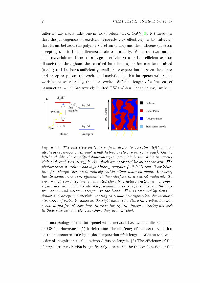
fullerene C60 was a milestone in the development of OSCs [3]. It turned out
that the photogenerated excitons dissociate very eectively at the interface
that forms between the polymer (electron donor) and the fullerene (electron
acceptor) due to their dierence in electron anity. When the two immis-
cible materials are blended, a large interfacial area and an ecient exciton
dissociation throughout the so-called bulk heterojunction can be obtained
(see gure 1.1). For a suciently small phase separation between the donor
and acceptor phase, the exciton dissociation in this interpenetrating net-
work is not restricted by the short exciton diusion length of a few tens of
nanometres, which has severely limited OSCs with a planar heterojunction.
hω
Donor
fasttransfer
e−
exciton
E
Acceptor
E1
2
E2
E1
E (D)
(D) (A)
(A)
Donor Phase
Cathode
Transparent Anode
Acceptor Phase100−
300n
m
Figure 1.1: The fast electron transfer from donor to acceptor (left) and anidealised cross-section through a bulk heterojunction solar cell (right). On theleft-hand side, the simplied donor-acceptor principle is shown for two mate-rials with each two energy levels, which are separated by an energy gap. Thephotogenerated exciton has high binding energies (>0.1eV) and dissociationinto free charge carriers is unlikely within either material alone. However,the dissociation is very ecient at the interface to a second material. Toensure that every exciton is generated close to a heterojunction a ne phaseseparation with a length scale of a few nanometres is required between the elec-tron donor and electron acceptor in the blend. This is obtained by blendingdonor and acceptor materials, leading to a bulk heterojunction the idealisedstructure, of which is shown on the right-hand side. Once the exciton has dis-sociated, the free charges have to move through the interpenetrating networkto their respective electrodes, where they are collected.
The morphology of this interpenetrating network has two signicant eects
on OSC performance. (1) It determines the eciency of exciton dissociation
on the nanometre scale by a phase separation with length scales on the same
order of magnitude as the exciton diusion length. (2) The eciency of the
charge carrier collection is signicantly determined by the combination of the
3
eect of the morphology on the charge carrier mobility and the formation of
a continuous path to the respective electrodes. Despite its importance for
the OSC performance, the morphology has not yet been fully determined.
Its dimensions require atomic force microscopy (AFM) and it is often not
possible to infer from the AFM surface the morphology in the bulk.
The major limiting factor for the materials used in OSCs at the moment is
the loss of nearly 1eV in energy during the dissociation of the exciton [4]. Ad-
ditionally, the large optical band gap of ≈2eV of the semiconductor materials
makes only a limited fraction of the solar spectrum available for harvesting.
Thus much research is focused on optimising the morphology of donor and
acceptor material and synthesising new materials with more appropriate en-
ergy levels and optical gaps. So far the highest power conversion eciency
reached at our laboratory is 3.5%. The highest certied η for an OSC is
3.0%, although values approaching 5% have been reported by other groups
in the literature [5].
Despite the progress of the previous years in qualitatively understanding
OSC behaviour, there are still many open questions regarding the funda-
mental physical understanding of the processes in an OSC as well as the
relation between the production parameters and their eects on OSC char-
acteristics. The experimental investigation of these issues is complicated by
the fact that generally an intentional variation of one single production pa-
rameter is dicult to realise. Due to the nature of the production process
there are generally other parameters with variations as well. These varia-
tions often aect the experimental results by the same order of magnitude
as the intended variation. Thus the characteristics observed in the measured
OSC data are dicult to attribute to a specic variation in the production
process. Although only a few steps are necessary to produce an OSC, these
steps have many degrees of freedom, which often exhibit a complex interde-
pendence. This complicates both the optimisation of the production steps
and the development of a statistically sound understanding of the physical
processes in an OSC.
Even when considering the same material combination of donor and accep-
tor, there are many parameters during production with a potential inuence
on the OSC performance and always several dier from one substrate to the
next. The eects of these variations have to be analysed simultaneously due
to the complexity and sensitivity of the OSCs. This makes the application of
4 CHAPTER 1. INTRODUCTION
multivariate methodology essential, because only partial information about
the OSC can be obtained when the eect of one parameter alone is consid-
ered. The creation of both an experimental infrastructure, which permits
a statistically sound analysis, and the use of principal component analysis
(PCA) as a multivariate statistical method is the primary new contribution
of this thesis to research on organic solar cells.
char
acte
risa
tion
met
hods
Aut
omat
ion
of th
e m
ain
OSC
tron
ic d
ata
man
agem
ent s
yste
mD
evel
opm
ent o
f an
effi
cien
t ele
c−
Stru
ctur
ing
and
stan
dard
isat
ion
of th
e O
SC p
rodu
ctio
n pr
oces
sStatistical analysis
production parameters and OSC propertiesof the interdependence between
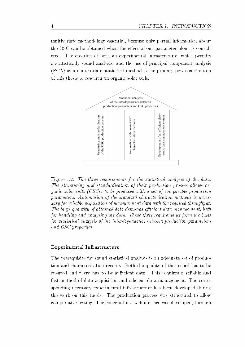
Figure 1.2: The three requirements for the statistical analysis of the data.The structuring and standardisation of their production process allows or-ganic solar cells (OSCs) to be produced with a set of comparable productionparameters. Automation of the standard characterisation methods is neces-sary for reliable acquisition of measurement data with the required throughput.The large quantity of obtained data demands ecient data management, bothfor handling and analysing the data. These three requirements form the basisfor statistical analysis of the interdependence between production parametersand OSC properties.
Experimental Infrastructure
The prerequisite for sound statistical analysis is an adequate set of produc-
tion and characterisation records. Both the quality of the record has to be
ensured and there has to be sucient data. This requires a reliable and
fast method of data acquisition and ecient data management. The corre-
sponding necessary experimental infrastructure has been developed during
the work on this thesis. The production process was structured to allow
comparative testing. The concept for a webinterface was developed, through
5
which the standardised logging of the production process is now carried out.
The main OSC characterisation methods current-voltage measurements,
spectral response measurements and absorption measurements were all in-
tegrated into one automated setup, which allows a reliable acquisition of
measurement data with the necessary high throughput. This is essential, at
the characterisation stage, to handle the many variations in production pa-
rameters both intentional and caused by usual uctuations which lead to
a large number of OSCs. The main hardware component of the automated
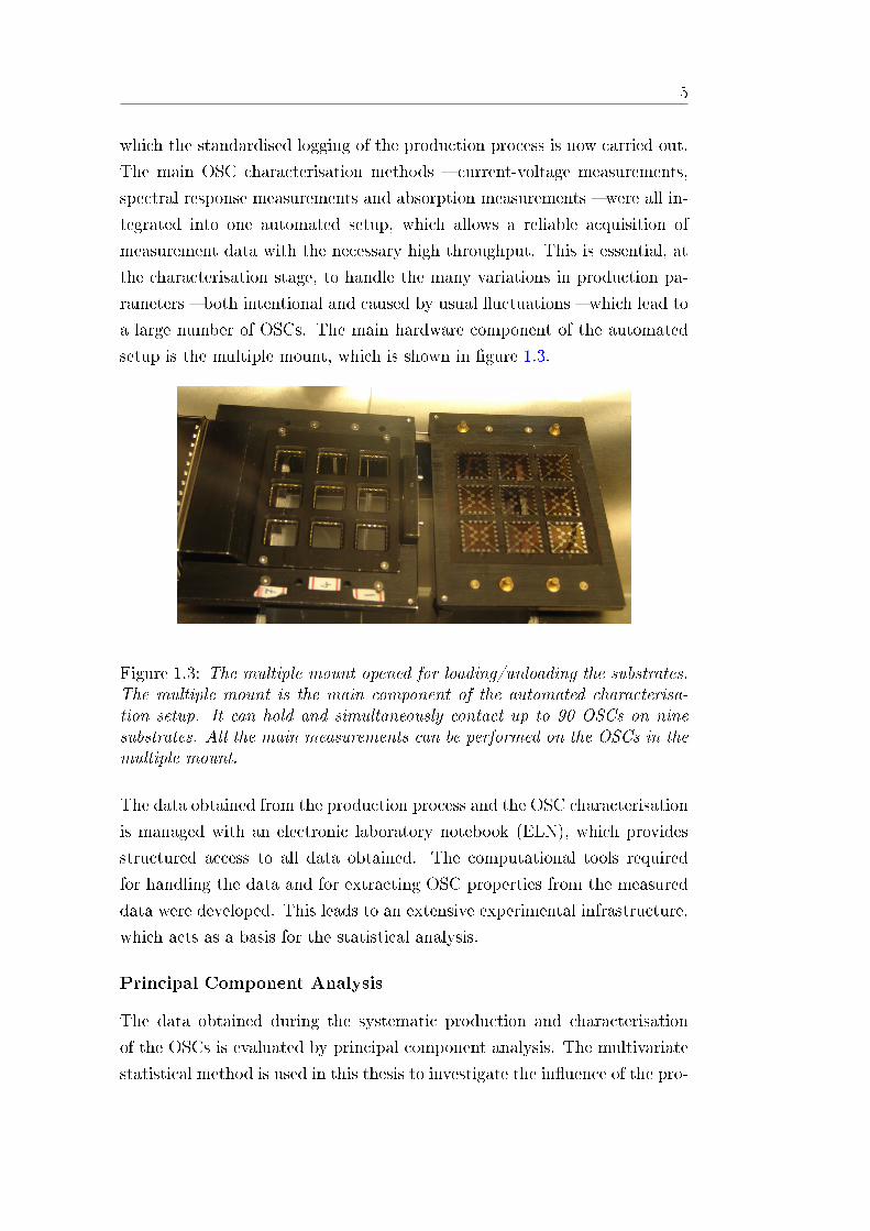
setup is the multiple mount, which is shown in gure 1.3.
Figure 1.3: The multiple mount opened for loading/unloading the substrates.The multiple mount is the main component of the automated characterisa-tion setup. It can hold and simultaneously contact up to 90 OSCs on ninesubstrates. All the main measurements can be performed on the OSCs in themultiple mount.
The data obtained from the production process and the OSC characterisation
is managed with an electronic laboratory notebook (ELN), which provides
structured access to all data obtained. The computational tools required
for handling the data and for extracting OSC properties from the measured
data were developed. This leads to an extensive experimental infrastructure,
which acts as a basis for the statistical analysis.
Principal Component Analysis
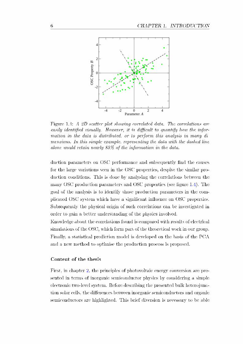
The data obtained during the systematic production and characterisation
of the OSCs is evaluated by principal component analysis. The multivariate
statistical method is used in this thesis to investigate the inuence of the pro-
6 CHAPTER 1. INTRODUCTION
-4 -2 0 2 4Parameter A
-4
-2
0
2
4
OSC
Pro
pert
y B
Tue Nov 28 13:21:39 2006
Figure 1.4: A 2D scatter plot showing correlated data. The correlations areeasily identied visually. However, it is dicult to quantify how the infor-mation in the data is distributed, or to perform this analysis in many di-mensions. In this simple example, representing the data with the dashed linealone would retain nearly 85% of the information in the data.
duction parameters on OSC performance and subsequently nd the causes
for the large variations seen in the OSC properties, despite the similar pro-
duction conditions. This is done by analysing the correlations between the
many OSC production parameters and OSC properties (see gure 1.4). The
goal of the analysis is to identify those production parameters in the com-
plicated OSC system which have a signicant inuence on OSC properties.
Subsequently the physical origin of such correlations can be investigated in
order to gain a better understanding of the physics involved.
Knowledge about the correlations found is compared with results of electrical
simulations of the OSC, which form part of the theoretical work in our group.
Finally, a statistical prediction model is developed on the basis of the PCA
and a new method to optimise the production process is proposed.
Content of the thesis
First, in chapter 2, the principles of photovoltaic energy conversion are pre-
sented in terms of inorganic semiconductor physics by considering a simple
electronic two-level system. Before describing the presented bulk heterojunc-
tion solar cells, the dierences between inorganic semiconductors and organic
semiconductors are highlighted. This brief diversion is necessary to be able
7
to present the physics of organic solar cells with their specic features. Two
approaches for modelling organic solar cells are presented.
Chapter 3 then introduces the investigated OSCs and focuses on their pro-
duction process. Each production step is described and the important pa-
rameters are presented. A detailed understanding of each step is necessary
in order to structure and standardise the recorded production parameters for
a comparable production process.
The characterisation methods used and the automation of these experiments
to allow a high and reliable throughput form the topic of chapter 4. The
principles of the standard characterisation methods are presented and mea-
surement uncertainties discussed. A reliable OSC characterisation system
with a high throughput is paramount for the ecient handling of many pa-
rameter variations during OSC production at the characterisation stage. This
requires automation of the main experiments, the components and perfor-
mance of which are presented.
The data analysis methods, which were used, and the computational tools
developed in order to eciently handle the large amount of data obtained
during production and characterisation, are the focus of chapter 5. The
methods used to analyse measurement data and the principal component
analysis (PCA) used to determine the interdependence between the produc-
tion process and the measured OSC properties are presented. The concept
of an electronic laboratory notebook (ELN) is introduced and the process of
the structured and standardised data acquisition, handling and processing is
described.
Chapters 3 to 5 describe the basis for reliable acquisition of measurement data
and thus sound data analysis, which is presented in chapter 6. A large run of
experiments with the smallest number of varying parameters allowed by the
production process was conducted. The main eects seen in the measured
data are described. Using PCA, the interdependence between production
parameters and measurement results is analysed and the results are discussed.
Finally, a statistical model based on the principal component analysis is
proposed to optimise the production process.

8 CHAPTER 1. INTRODUCTION
Chapter 2
Fundamentals
The important concepts for the physics of organic solar cells (OSC) will be
presented here. A simple and general electronic model for a solar cell is
used to describe the basic processes for the conversion of the energy of light
into electrical work. Then the discussion moves to the special properties of
organic semiconductors and solar cells made of these materials. The main
steps of the solar energy conversion in OSCs are described and the current
state of research is presented.
2.1 Solar Cell Model System
The key issue of all currently investigated solar cells is the optimal use of
semiconductor material. The special feature of semiconductors both from
inorganic and organic materials are two quasi-continua of charge carrier
transport levels, which are separated by an energy exceeding by far kBT at
moderate temperatures T (kBT at room temperatures ≈ 0.26meV). The en-
ergetically lower quasi-continuum is nearly completely lled with electrons,
whereas the upper one is nearly empty. They are called quasi-continua,
because the energetic distance between the discrete levels within a quasi-
continuum is much smaller than kBT . The region between the quasi-continua
is called forbidden region or energy gap EG, because it has no available elec-
tronic levels. The simple electronic model system of a semiconductor with
two levels is shown in gure 2.1. In inorganic semiconductors the lower level
is called the valence band and consists of occupied binding levels. These
electronic levels are delocalised over the whole semiconductor in the ideal
case due to perfect crystallinity. In organic semiconductors the basic enti-
ties are molecules and the delocalisation of the levels, which is responsible
9
10 CHAPTER 2. FUNDAMENTALS
ConductionBand
Valence
Band
HOMO
LUMO
Vacuum Level0
E
CE
EV
GE
Figure 2.1: A simple two-level model system as an example for the descriptionof the basic processes in a solar cell. In the case of organic semiconductors,the valence band (energy at edge EV ) corresponds to the Highest OccupiedMolecular Orbital (HOMO) and the conduction band (energy at edge EC)Lowest Unoccupied Molecular Orbital (LUMO). The two levels are separatedby a gap of width EG without any available electronic states.
for the semiconductor behaviour, is much less pronounced due to the weak
Van-der-Waals binding. Here the bands are formed by the occupied binding
orbitals of the single molecules, the so-called molecular orbitals (MO). The
HOMO (Highest Occupied Molecular Orbital) in molecular semiconductors
corresponds to the edge of the valence band in inorganic semiconductors.
However, for simplicity, the whole quasi-continuum of occupied binding lev-
els is often called HOMO. The energetically higher lying quasi-continuum is
nearly completely empty and is called conduction band. This corresponds
to the LUMO (Lowest Unoccupied Molecular Orbital) in the molecular pic-
ture. Although the physics derived for inorganic semiconductors can only
be applied to a certain extent to organic semiconductors, the basic solar cell
principles can be described with the help of the model two-level system shown
above following Würfel [6] and Sze [7].
2.1.1 Thermal Equilibrium in a Semiconductor
In thermal equilibrium in the dark, the probability of electron occupation
fF (E) of one-electron states with energy E is described by the Fermi-Dirac
2.1. SOLAR CELL MODEL SYSTEM 11
distribution:
fF (E) =1
exp(
E−EF
kBT
)+ 1
, (2.1)
where T denotes the temperature of the black body radiation. A state with
energy at the Fermi energy EF hence has an occupation probability of 1/2
as evident from equation 2.1. The occupation probability of electronic states
a few kBT below EF is nearly unity at moderate temperatures, whereas a
few kBT above EF it is nearly zero. In order to calculate the number n
of electrons per unit volume in the energy interval [E , E + dE ], the states'occupation probability fF (E) has to be multiplied by the density of states
De(E) in this energy interval. Hence the density of electrons between E and
E + dE is then given by:
dn(E) = De(E)fF (E)dE . (2.2)
Intrinsic (undoped) semiconductors used for solar energy conversion feature
a Fermi energy which lies within the gap many kBT away from the conduc-
tion and valence band edge. As the occupation probability is nearly zero
a few kBT above EF , the Fermi distribution fF (E) in equation 2.2 can be
approximated for EC − EF > 3/2kBT by the Boltzmann distribution
fB(E) = exp
(−E − EF
kBT
). (2.3)
Therefore the electron density in the conduction band is given by
n =
∞∫EC
De(E)fB(E)dE ≈ NC exp
(−EC − EF
kBT
). (2.4)
EC is the energy of the conduction band edge and NC , called the eective
density of states of the conduction band, contains the constant factors of
integration. This simplication of equation 2.2 is valid as long as n is small
compared to NC .
The occupation probability for energies E lying a few kBT below EF is ac-
cording to equation 2.1 nearly unity. Rather than describing single electrons
in the valence band, unoccupied one-electron states of the valence band can
be described as missing electrons or holes. Thus they have the same density
of states as the electrons. This way the number of particles which need to
12 CHAPTER 2. FUNDAMENTALS
be described, is reduced by several orders of magnitude and some symmetry
in the description is introduced. The density of holes in the valence band
is therefore, analogous to calculating the electron density in the conduction
band, given by
p =
EV∫−∞
De(E)(1− fF (E))dE ≈ NV exp
(−EF − EV
kBT
), (2.5)
where EV is the energy of the valence band edge and NV is the eective
density of states of the valence band.
An important relation can be obtained by combining equations 2.4 and 2.5
to
n2i = np = NCNV exp
(− EG
kBT
), (2.6)
where ni being the intrinsic charge carrier density, which is a constant prop-
erty of the material, and EG = EC − EV . The product np is independent
of the position of the Fermi level and hence cannot be altered by doping the
semiconductor. For an intrinsic semiconductor all electrons in the conduction
band originate from the valence band and hence p = n. Using this equality
and equations 2.4 and 2.5, the position of the Fermi energy EF relative to
valence and conduction band can be calculated as follows:
EF =1
2(EV + EC) +
1
2kBT ln
NV
NC
. (2.7)
At low temperature or at NV ≈ NC the Fermi level of a intrinsic semicon-
ductor is in the middle of the gap.
2.1.2 Semiconductor under Illumination
Illuminating the described model system with photons of energy higher than
EG creates additional charge carriers in the system. The system is then not in
equilibrium with the ambient, but with the light source. If the photons have
an energy ~ω > EG, electrons in the valence band can absorb photons and be
excited to the conduction band. This leaves a hole in the valence band and the
number of both electrons and holes grows by the same amount, as determined
by the charge carrier generation rate G. The relaxation between both bands
is relatively slow due to the large energy dierence and happens in the ideal
case only through radiative recombination of electrons and holes. However,
2.1. SOLAR CELL MODEL SYSTEM 13
within the bands the thermal relaxation is rapid, resulting in two dierent
Fermi distributions, one for electrons in the conduction band, another for
holes in the valence band. The corresponding charge carrier densities can be
derived analogous to equation 2.4 and 2.5, leading to
n = NC exp
(−EC − EF,C
kBT
), (2.8a)
p = NV exp
(−EF,V − EV
kBT
), (2.8b)
where EF,C is called electron quasi-Fermi level (n-QFL) and EF,V hole quasi-
Fermi Level (p-QFL) respectively. The product np now exceeds n2i (equa-
tion 2.6). The average energy, which can be extracted from an electron-hole
pair is equal to the dierence of the Fermi energies of valence and conduction
band, EF,V and EF,C respectively
EF,C − EF,V = EG + kBT lnnp
NCNV︸ ︷︷ ︸<0
. (2.9)
With increasing illumination, hence with increasing number of charge carri-
ers, the splitting of the QFL increases. However neither occupation proba-
bility can reach 1/2 in a semiconductor with only one gap. The splitting of
the Fermi energies remains always smaller than EG, because the excitation
competes with two eects: spontaneous emission and stimulated emission.
Both are getting more likely with increasing charge carrier densities. In the
two-level model system all three eects, i.e. absorption, spontaneous and
stimulated emission, are all connected via the Einstein coecients.
The simplest case of spontaneous decay processes is the radiative recombi-
nation of electrons and holes, leading to photoluminescence (PL). Without
external inuence, an electron decays directly from the conduction band to
the valence band and recombines with a hole emitting a photon of energy
~ω = EG. The recombination rate R per unit volume is given by
R = r(np− n2i ), (2.10)
with radiative recombination constant r. In equation 2.10 the number of
intrinsic charge carriers is subtracted, because only excess charge carriers
(with respect to the equilibrium case) lead to recombination.
14 CHAPTER 2. FUNDAMENTALS
The second eect is the stimulated emission. It describes the transfer of an
electron from the conduction band to the valence band due to the stimulation
of an atom by an incoming photon. When the excited state is perturbed
by the incoming photon, a second photon with the same wavefunction as
the stimulating photon can be emitted and the formerly excited state then
returns into its ground state. As before, this process is getting more likely
with increasing occupation of the conduction band and increasing photon
density with energies close to EG.
2.1.3 Charge Carrier Extraction at the Contacts
So far the model semiconductor has been considered without contacts and
the charges could not leave the system. Under illumination extra charges
are generated in the semiconductor and the energy of the absorbed light
is stored as chemical potential energy in the system. Suitable contacts are
required to extract these charges for converting the chemical potential energy
into electrical energy. Ideal contacts, i.e. contacts at which no charges and
no energy are lost during charge carrier extraction, have to satisfy following
requirements:
1. The contacts have to be semipermeable, i.e. only permeable for the
respective type of charge carriers. This guarantees that no current is
lost at the contacts.
2. The Fermi levels of the contacts have to match the QFL of their re-
spective charge carriers. This way no chemical potential energy is lost
during charge carrier extraction.
The second condition is however only valid if transport problems on the way
to the electrodes can be neglected, i.e. if no energy is lost on the way to the
contacts.
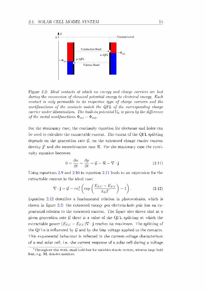
Contacts: The Ideal Case
The case of ideal contacts is shown in gure 2.2. Both contacts have semiper-
meable membranes and hence allow only the selective passage of the respec-
tive charge carriers. The workfunctions Φm, i.e. the Fermi levels of the
contacting metal, match the QFLs of the allowed charge carrier at the mem-
branes. Their dierence, Φm1 − Φm2, denes the built-in potential Vbi.
2.1. SOLAR CELL MODEL SYSTEM 15
m1Φ
Vacuum Level
n−QFL
p−QFL
0
E
Valence Band
Conduction Band
− Φm2
−
Figure 2.2: Ideal contacts at which no energy and charge carriers are lostduring the conversion of chemical potential energy to electrical energy. Eachcontact is only permeable to its respective type of charge carriers and theworkfunctions of the contacts match the QFL of the corresponding chargecarrier under illumination. The built-in potential Vbi is given by the dierenceof the metal workfunctions Φm1 − Φm2.
For the stationary case, the continuity equation for electrons and holes can
be used to calculate the extractable current. The extent of the QFL splitting
depends on the generation rate G, on the extracted charge carrier current
density j1 and the recombination rate R. For the stationary case the conti-
nuity equation becomes:
0 =∂n
∂t=
∂p
∂t= G −R−∇ · j (2.11)
Using equations 2.9 and 2.10 in equation 2.11 leads to an expression for the
extractable current in the ideal case:
∇ · j = G − rn2i
(exp
(EF,C − EF,V
kBT
)− 1
). (2.12)
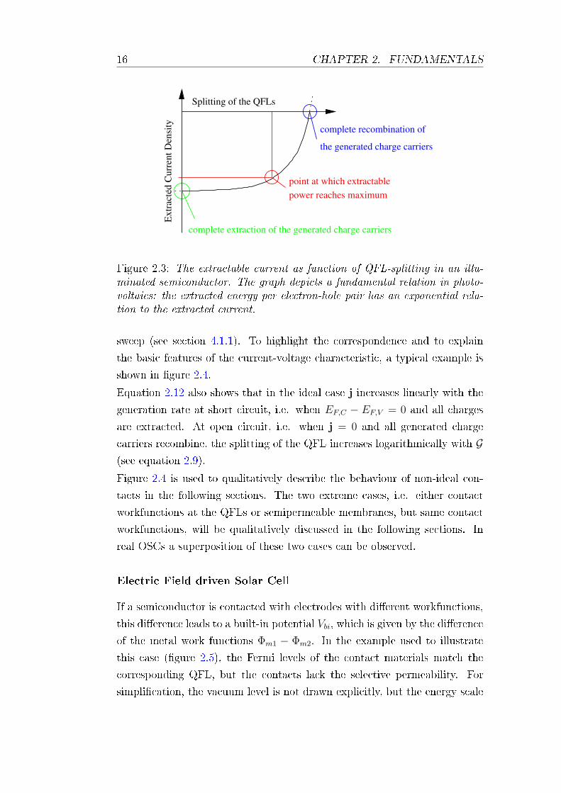
Equation 2.12 describes a fundamental relation in photovoltaics, which is
shown in gure 2.3: the extracted energy per electron-hole pair has an ex-
ponential relation to the extracted current. The gure also shows that at a
given generation rate G there is a value of the QFL splitting at which the
extractable power (EF,C − EF,V )∇ · j reaches its maximum. The splitting ofthe QFLs is inuenced by G and by the bias voltage applied to the contacts.
This exponential behaviour is reected in the current-voltage characteristic
of a real solar cell, i.e. the current response of a solar cell during a voltage1Throughout this work, small bold font for variables denote vectors, whereas large bold
font, e.g. M, denotes matrices.
16 CHAPTER 2. FUNDAMENTALS
point at which extractablepower reaches maximum
complete extraction of the generated charge carriers
the generated charge carriers
complete recombination of
Splitting of the QFLs
Ext
ract
ed C
urre
nt D
ensi
ty
Figure 2.3: The extractable current as function of QFL-splitting in an illu-minated semiconductor. The graph depicts a fundamental relation in photo-voltaics: the extracted energy per electron-hole pair has an exponential rela-tion to the extracted current.
sweep (see section 4.1.1). To highlight the correspondence and to explain
the basic features of the current-voltage characteristic, a typical example is
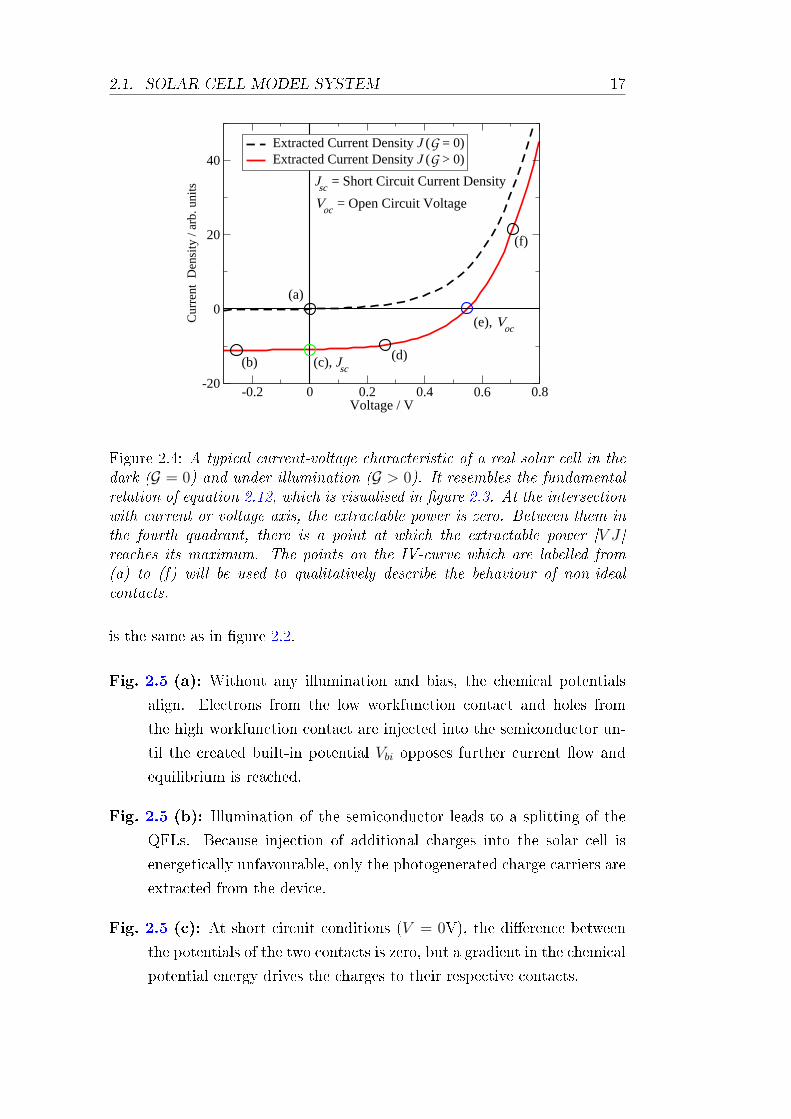
shown in gure 2.4.
Equation 2.12 also shows that in the ideal case j increases linearly with the
generation rate at short circuit, i.e. when EF,C − EF,V = 0 and all charges
are extracted. At open circuit, i.e. when j = 0 and all generated charge
carriers recombine, the splitting of the QFL increases logarithmically with G(see equation 2.9).
Figure 2.4 is used to qualitatively describe the behaviour of non-ideal con-
tacts in the following sections. The two extreme cases, i.e. either contact
workfunctions at the QFLs or semipermeable membranes, but same contact
workfunctions, will be qualitatively discussed in the following sections. In
real OSCs a superposition of these two cases can be observed.
Electric Field driven Solar Cell
If a semiconductor is contacted with electrodes with dierent workfunctions,
this dierence leads to a built-in potential Vbi, which is given by the dierence
of the metal work functions Φm1 − Φm2. In the example used to illustrate
this case (gure 2.5), the Fermi levels of the contact materials match the
corresponding QFL, but the contacts lack the selective permeability. For
simplication, the vacuum level is not drawn explicitly, but the energy scale
2.1. SOLAR CELL MODEL SYSTEM 17
-0.2 0 0.2 0.4 0.6 0.8Voltage / V
-20
0
20
40
Cur
rent
Den
sity
/ ar
b. u
nits
Extracted Current Density J (G = 0)Extracted Current Density J (G > 0)
(b) (c), Jsc(d)
(e), Voc
(f)
Voc = Open Circuit Voltage
Jsc = Short Circuit Current Density
(a)
Fri Nov 24 22:07:35 2006
Figure 2.4: A typical current-voltage characteristic of a real solar cell in thedark (G = 0) and under illumination (G > 0). It resembles the fundamentalrelation of equation 2.12, which is visualised in gure 2.3. At the intersectionwith current or voltage axis, the extractable power is zero. Between them inthe fourth quadrant, there is a point at which the extractable power |V J |reaches its maximum. The points on the IV-curve which are labelled from(a) to (f) will be used to qualitatively describe the behaviour of non-idealcontacts.
is the same as in gure 2.2.
Fig. 2.5 (a): Without any illumination and bias, the chemical potentials
align. Electrons from the low workfunction contact and holes from
the high workfunction contact are injected into the semiconductor un-
til the created built-in potential Vbi opposes further current ow and
equilibrium is reached.
Fig. 2.5 (b): Illumination of the semiconductor leads to a splitting of the
QFLs. Because injection of additional charges into the solar cell is
energetically unfavourable, only the photogenerated charge carriers are
extracted from the device.
Fig. 2.5 (c): At short circuit conditions (V = 0V), the dierence between
the potentials of the two contacts is zero, but a gradient in the chemical
potential energy drives the charges to their respective contacts.
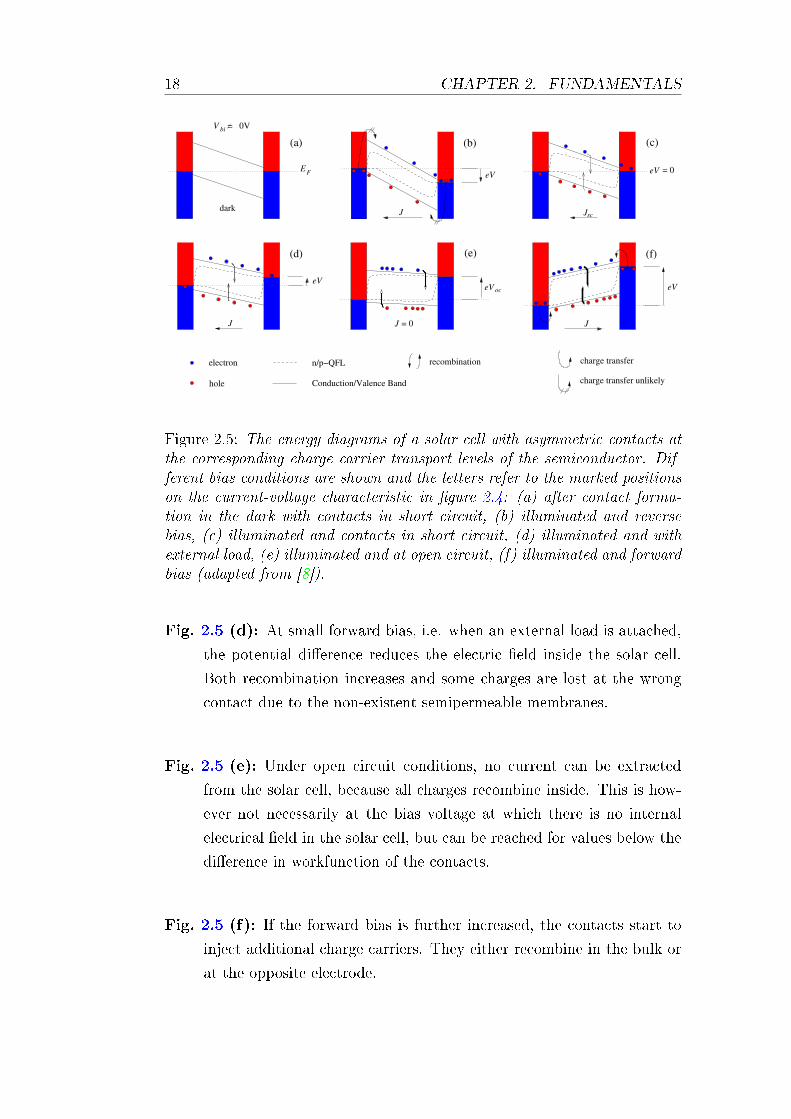
18 CHAPTER 2. FUNDAMENTALS
eV
J
J
eV
J
(a) (b)
(d)
eV
FeV
charge transfer unlikely
recombinationn/p−QFL
hole
electron charge transfer
(c)
(f)(e)
oc
Conduction/Valence Band
darkscJ
J
eV = 0
biV = 0V
E
= 0
Figure 2.5: The energy diagrams of a solar cell with asymmetric contacts atthe corresponding charge carrier transport levels of the semiconductor. Dif-ferent bias conditions are shown and the letters refer to the marked positionson the current-voltage characteristic in gure 2.4: (a) after contact forma-tion in the dark with contacts in short circuit, (b) illuminated and reversebias, (c) illuminated and contacts in short circuit, (d) illuminated and withexternal load, (e) illuminated and at open circuit, (f) illuminated and forwardbias (adapted from [8]).
Fig. 2.5 (d): At small forward bias, i.e. when an external load is attached,
the potential dierence reduces the electric eld inside the solar cell.
Both recombination increases and some charges are lost at the wrong
contact due to the non-existent semipermeable membranes.
Fig. 2.5 (e): Under open circuit conditions, no current can be extracted
from the solar cell, because all charges recombine inside. This is how-
ever not necessarily at the bias voltage at which there is no internal
electrical eld in the solar cell, but can be reached for values below the
dierence in workfunction of the contacts.
Fig. 2.5 (f): If the forward bias is further increased, the contacts start to
inject additional charge carriers. They either recombine in the bulk or
at the opposite electrode.
2.1. SOLAR CELL MODEL SYSTEM 19
Solar Cell with semipermeable Membranes
The opposite extreme case is given, if the contacts are semipermeable, but
have the same workfunction, which does not match either QFL in the semi-
conductor. The resulting built-in eld Vbi is zero. Assuming symmetric Fermi
levels of the contacting material located in the middle of the gap, the eects
can be illustrated with gure 2.6, which shows the band diagram of a semi-
conductor at dierent bias conditions. Again for simplicity the vacuum level
is not shown (see gure 2.2).
sc
eV
eV
eV
(a) (b)
(d) (e)
(c)
eV
EF
eV
charge transferrecombinationn/p−QFLelectron
membrane
oc
(f)
hole
J J
J J
Conduction/Valence Band
dark
= 0
J = 0
Vbi
= 0V
Figure 2.6: The energy diagrams of a solar cell with semipermeable mem-branes and symmetric contacts under dierent bias conditions. The letters re-fer to the marked positions on the current-voltage characteristic in gure 2.4:(a) after contact formation in the dark without bias, (b) illuminated and re-verse bias, (c) illuminated and contacts in short circuit, (d) illuminated andwith external load, (e) illuminated and at open circuit, (f) illuminated andforward bias (adapted from [8]).
Fig. 2.6 (a): Without any illumination and bias, the Fermi level is constant
throughout the semiconductor and equals the work functions of the
contacts. The resulting built-in potential Vbi = 0. The system is in
thermal equilibrium with the ambient at temperature T .
Fig. 2.6 (b): Illumination of the semiconductor leads to a splitting of the
QFLs due to the photogenerated charge carriers. Applying a reverse
20 CHAPTER 2. FUNDAMENTALS
bias under illumination leads to a quick extraction of nearly all photo-
generated charge carriers and recombination can largely be neglected.
Fig. 2.6 (c): At short circuit conditions, the internal electrical eld is zero,
but the concentration gradient, which builds up due to accumulation
of charges at their non-permeable contact, drives the charge carrier to
their respective contact. As the charge carrier concentration in the
device rises, recombination increases and not all charges are extracted.
Fig. 2.6 (d): At small forward bias, i.e. when a small external load is at-
tached, the electrical eld opposes the diusion. The diusion gradient
of the QFLs however still drives the charge carriers to their respective
electrode, but recombination rises further.
Fig. 2.6 (e): Under open circuit conditions, no current can be extracted
from the solar cell, because all charge carriers recombine in the bulk.
The open circuit voltage equals the dierence between the two QFLs
at the contacts.
Fig. 2.6 (f): If the forward bias is further increased, the contacts start to
inject charge carriers, which accumulate at the opposite electrode. The
charges cannot recombine at the surface of the membranes, but only in
the bulk.
2.2 Organic Semiconductors
Before describing the particular processes of the solar energy conversion in
OSCs, it is necessary to highlight the dierences between organic, i.e. carbon-
based, and inorganic semiconductors, e.g. silicon.
The conducting and semiconducting properties of polymers were discovered
when poly-acetylene (PA, see gure 2.7, left), a simple polymer, was acci-
dentally doped with iodine concentrations, which were three orders of mag-
nitude larger than intended [2]. It turned out that with high doping levels,
PA changed from being an insulator to being a good conductor, an eect,
which had not been observed in polymers before. This conducting and semi-
conducting behaviour was subsequently found in other polymers as well and
it was possible to create new materials with these properties. The common
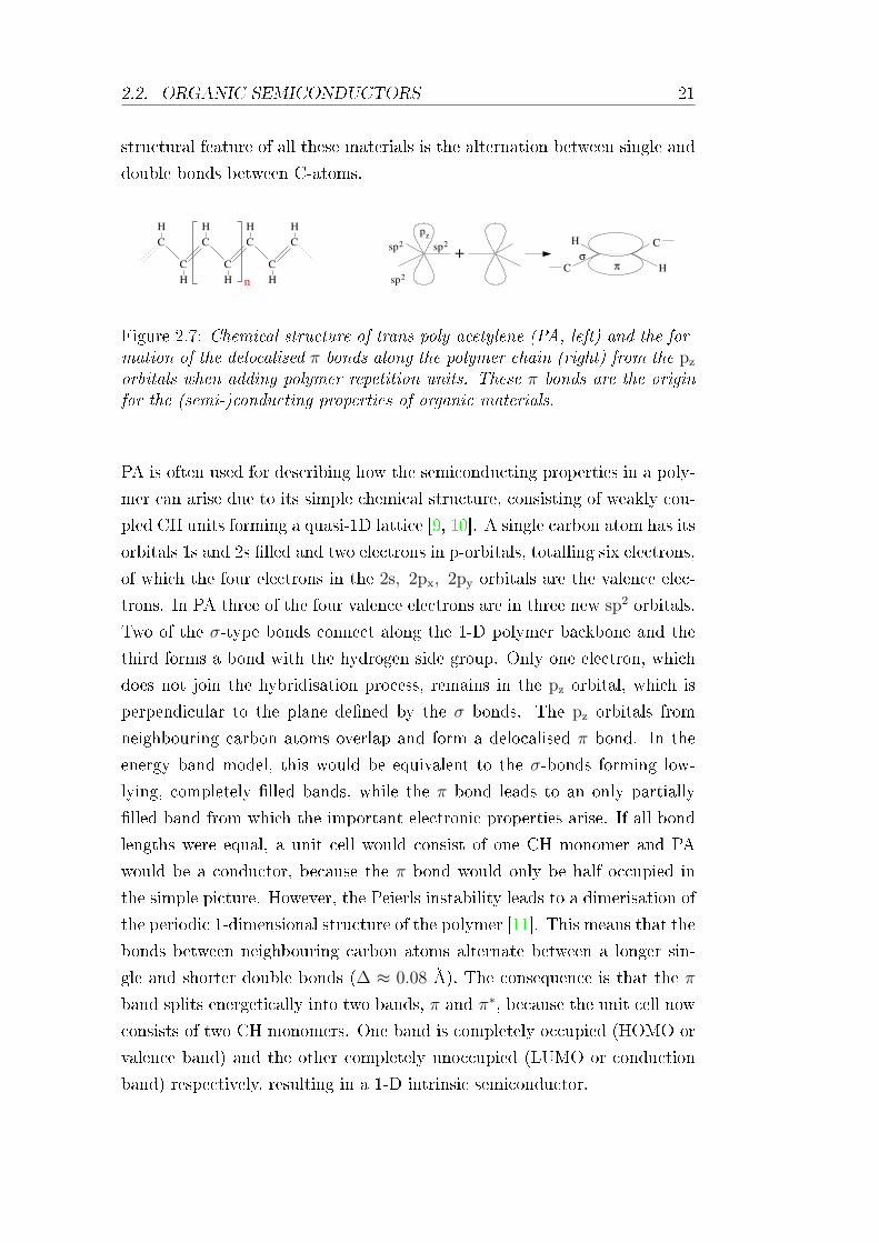
2.2. ORGANIC SEMICONDUCTORS 21
structural feature of all these materials is the alternation between single and
double bonds between C-atoms.
CC C
C CC
H
H
H H
H HC
H
nπ
σ
C
H C
Hsp2
sp2 sp2pz
+
Figure 2.7: Chemical structure of trans-poly-acetylene (PA, left) and the for-mation of the delocalised π bonds along the polymer chain (right) from the pz
orbitals when adding polymer repetition units. These π bonds are the originfor the (semi-)conducting properties of organic materials.
PA is often used for describing how the semiconducting properties in a poly-
mer can arise due to its simple chemical structure, consisting of weakly cou-
pled CH units forming a quasi-1D lattice [9, 10]. A single carbon atom has its
orbitals 1s and 2s lled and two electrons in p-orbitals, totalling six electrons,
of which the four electrons in the 2s, 2px, 2py orbitals are the valence elec-
trons. In PA three of the four valence electrons are in three new sp2 orbitals.
Two of the σ-type bonds connect along the 1-D polymer backbone and the
third forms a bond with the hydrogen side group. Only one electron, which
does not join the hybridisation process, remains in the pz orbital, which is
perpendicular to the plane dened by the σ bonds. The pz orbitals from
neighbouring carbon atoms overlap and form a delocalised π bond. In the
energy band model, this would be equivalent to the σ-bonds forming low-
lying, completely lled bands, while the π bond leads to an only partially
lled band from which the important electronic properties arise. If all bond
lengths were equal, a unit cell would consist of one CH monomer and PA
would be a conductor, because the π bond would only be half occupied in
the simple picture. However, the Peierls instability leads to a dimerisation of
the periodic 1-dimensional structure of the polymer [11]. This means that the
bonds between neighbouring carbon atoms alternate between a longer sin-
gle and shorter double bonds (∆ ≈ 0.08 Å). The consequence is that the π
band splits energetically into two bands, π and π∗, because the unit cell now
consists of two CH monomers. One band is completely occupied (HOMO or
valence band) and the other completely unoccupied (LUMO or conduction
band) respectively, resulting in a 1-D intrinsic semiconductor.
22 CHAPTER 2. FUNDAMENTALS
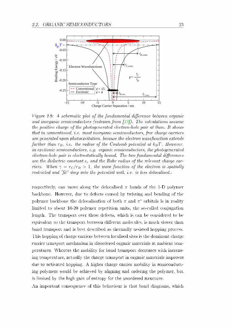
2.2.1 Excitations
Due to the low dielectric constant (εr ≈3-4) compared to most inorganic
semiconductors (>10) and the small overlap of the molecular orbitals, or-
ganic semiconductors are characterised by strongly bound excited states.
Excitons, as the excited states are best described as, thus have Coulombic
binding energies ranging from about 100meV to 1eV and are localised on
a few polymer repetition units or a molecule [12]. The exciton is electrical
neutral and thus to rst order unaected by external electric elds and thus
moves by diusion. For inorganic semiconductors typical binding energies of
photogenerated electron-hole pairs are typically far below kBT (ca. 26meV
at room temperatures) such that free charge carriers are generated upon
photoexcitation due to thermal dissociation. Figure 2.8 illustrates this fun-
damental dierence. The categorisation into conventional semiconductors,
i.e. most inorganic, and excitonic semiconductors, which includes organic
semiconductors, has been done by the ratio of the width rC of the Coulom-
bic potential well at kBT and the Bohr radius of the relevant charge carrier
rB [13]:
γ =
(rC
rB
)≈(
e2
4πε0kBr0me
)(meff
ε2rT
), (2.13)
where e is the electronic charge, ε0 the permittivity of free space, r0 the
rst Bohr radius of an electron of the hydrogen atom, me the mass of the
electron and meff the eective electron mass in the semiconductor. If γ > 1
an excitonic behaviour is observed.
An important consequence of the locally bound exciton is the strong inter-
action with the lattice. The promotion of an electron from valence state to
conduction state and the connement of the resulting anti-bonding wave-
function to a small number of carbon atoms leads to a large rearrangement
of the valence electrons. As result, the local bond lengths change, which
subsequently aects both optical and electronic properties.
2.2.2 Charge Carriers and Charge Carrier Transport
The free charge carriers in organic materials are also localised to within a
few polymer repetition units or a molecular unit and strongly couple to the
lattice, which locally changes both optical and electronic properties of the
material. These charges, i.e. electrons and holes in the π∗ and π orbitals
2.2. ORGANIC SEMICONDUCTORS 23
-15 -10 -5 0 5 10 15Charge Carrier Separation / nm
-0.25
-0.20
-0.15
-0.10
-0.05
0.00
Bin
ding
Ene
rgy
/ eV
ConventionalExcitonic
kBT
Electron Wavefunctions
rC ,exc.rB ,exc.
rB ,conv.
rC ,conv.
ε = 4ε = 15
Semiconductor Type
γ = rCrB
Tue Nov 28 12:57:13 2006
Figure 2.8: A schematic plot of the fundamental dierence between organicand inorganic semiconductors (redrawn from [13]). The calculations assumethe positive charge of the photogenerated electron-hole pair at 0nm. It showsthat in conventional, i.e. most inorganic semiconductors, free charge carriersare generated upon photoexcitation, because the electron wavefunction extendsfurther than rB, i.e. the radius of the Coulomb potential at kBT . However,in excitonic semiconductors, e.g. organic semiconductors, the photogeneratedelectron-hole pair is electrostatically bound. The two fundamental dierencesare the dielectric constant εr and the Bohr radius of the relevant charge car-riers. When γ = rC/rB > 1, the wave function of the electron is spatiallyrestricted and t deep into the potential well, i.e. is less delocalised..
respectively, can move along the delocalised π bands of the 1-D polymer
backbone. However, due to defects caused by twisting and bending of the
polymer backbone the delocalisation of both π and π∗ orbitals is in reality
limited to about 10-20 polymer repetition units, the so-called conjugation
length. The transport over these defects, which is can be considered to be
equivalent to the transport between dierent molecules, is much slower than
band transport and is best described as thermally assisted hopping process.
This hopping of charge carriers between localised sites is the dominant charge
carrier transport mechanism in disordered organic materials at ambient tem-
peratures. Whereas the mobility for band transport decreases with increas-
ing temperature, actually the charge transport in organic materials improves
due to activated hopping. A higher charge carrier mobility in semiconduct-
ing polymers would be achieved by aligning and ordering the polymer, but
is limited by the high gain of entropy for the unordered structure.
An important consequence of this behaviour is that band diagrams, which
24 CHAPTER 2. FUNDAMENTALS
are often used for representing semiconducting polymers, can only be a crude
approximation of the available energies. They do not imply that there is band
transport nor that the energy levels remain the same in presence of charge
carriers.
The experimental investigation of the charge carrier transport is dicult.
Both electrical and optical properties of the material can be highly anisotropic
through the 1-D nature of the electronic system and the measured mobilities
strongly depend on both the morphology of the material, i.e. the arrange-
ment of the molecules, and the method used [14].
There are currently two models describing the hopping transport between
two localised orbitals, i.e. over a defect on the polymer backbone, between
dierent molecules: the Miller-Abrahams model [15] and the diabatic model
based on the electron transfer theory of Marcus [16].
In the Miller-Abrahams model the transfer rate ωij from hopping site i to j
with energy Ei and Ej respectively are given by:
ωij = ω0|Vij|2
exp(−(Ej−Ei)
kBT) if Ej > Ei
1 otherwise(2.14)
If sites i and j have the same energy, the transfer rate is simply given by
the product of proportion ω0 and the square of the overlap integral of the
electronic wavefunctions |Vij|2. If the nal state is higher in energy than
the starting state, the transfer rate is reduced by the Boltzmann factor.
Since organic molecules are only bound by Van-der-Waals forces, the distance
dependence of the overlap integral can be approximated by
|Vij|2 ∝ exp(−2ζ|Rij|) (2.15)
where Rij is the distance between both electron orbital centres of site i and j
and ζ is proportional to the inverse of the localisation radius of the orbitals.
The diabatic model is a result of rst order perturbation theory [16]. The
hopping rate from site i to j is given by:
ωij = |Vij|2√
π
~kBTEλ
exp
(−(Ei − Ej − Eλ)
2
4kBTEλ
). (2.16)
The reorganisation energy, Eλ, is a parameter of the material, which is de-
termined by the vibrational modes of the molecules in the mixed phase.
Contrary to the Miller-Abrahams model hopping events between states with
2.2. ORGANIC SEMICONDUCTORS 25
lower energy and states of higher energy can be thermally activated and get
faster with increasing temperature.
Despite their dierences, both models satisfy the requirements for a detailed
balance, i.e. there are no sinks or sources in the charge carrier ow in both
models. Monte-Carlo simulations for systems with Gauss-distributed spatial
and energetic disorder have shown that the mobility µ increases signicantly
for high electric elds for both models, while being constant for small (in this
context) electric elds (up to ca. 0.3MV/cm) [17, 18]. The typical electric
elds in OSC are in the order of 0.1 MV/cm.
Organic Semiconductors for OSCs
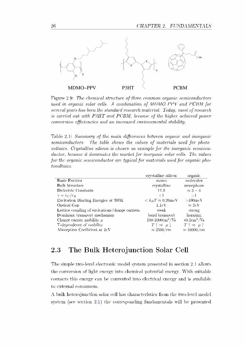
The structures of three common organic semiconductors used for organic
solar cells are shown in gure 2.9: poly(2-methoxy-5-(3,7-dimethyloctyloxy)-
1,4-phenylene vinylene) (MDMO-PPV), regioregular poly(3-hexylthiophene)
(RR-P3HT) and the fullerene derivative 1-(3-methoxycarbonyl)-propyl-1-1-
phenyl-(6,6)C61 (PCBM). The rst two are semiconducting polymers, like
PA. The last one belongs to the group of semiconducting molecules. The
structure of the materials is more complex than the one of PA, but they
share the same structural feature of alternating single and double carbon
bonds. The mechanism of charge transport is similar and dominated by
hopping.
Regioregular means that the alkyl side chains of the P3HT are aligned in a
periodic structure as opposed to the regiorandom case. PPV and Polythio-
phene are the actual conjugated polymer backbones, and the additions label
the side chains. The primary use of the side chains is to make the materials
soluble in organic solvents. Without side chains the polymer would hardly
or not at all be soluble and therefore very dicult to process from solution.
Additionally, the side chains can change the electro-optical properties of the
materials and thus be used to tune the materials. Finally, the morphology in
the solid is crucially inuenced by the regularity of the side chains [19]. The
fullerene derivative PCBM has so far shown the best OSC results in combi-
nation with polymers [20]. Again the functional side group is necessary to
make the material soluble.
26 CHAPTER 2. FUNDAMENTALS
n
MDMO−PPV P3HT PCBM
n
SS
O
O Me
Figure 2.9: The chemical structure of three common organic semiconductorsused in organic solar cells. A combination of MDMO-PPV and PCBM forseveral years has been the standard research material. Today, most of researchis carried out with P3HT and PCBM, because of the higher achieved powerconversion eciencies and an increased environmental stability.
Table 2.1: Summary of the main dierences between organic and inorganicsemiconductors. The table shows the values of materials used for photo-voltaics. Crystalline silicon is chosen as example for the inorganic semicon-ductor, because it dominates the market for inorganic solar cells. The valuesfor the organic semiconductor are typical for materials used for organic pho-tovoltaics.
crystalline silicon organicBasic Entities atoms moleculesBulk Structure crystalline amorphousDielectric Constants 11.9 ≈ 3− 4γ = rC/rB <1 >1Excitation Binding Energies at 300K < kBT ≈ 0.26meV >100meVOptical Gap 1.1eV ≈ 2eVLattice coupling of excitations/charge carriers weak strongDominant transport mechanism band transport hoppingCharge carrier mobility µ 100-1000cm2/Vs 0.1cm2/VsT-dependence of mobility T ↑ ⇒ µ ↓ T ↑ ⇒ µ ↑Absorption Coecient at 2eV ≈ 2500/cm ≈ 16000/cm
2.3 The Bulk Heterojunction Solar Cell
The simple two-level electronic model system presented in section 2.1 allows
the conversion of light energy into chemical potential energy. With suitable
contacts this energy can be converted into electrical energy and is available
to external consumers.
A bulk heterojunction solar cell has characteristics from the two-level model
system (see section 2.1) the corresponding fundamentals will be presented
2.3. THE BULK HETEROJUNCTION SOLAR CELL 27
in the following sections. Its core feature is the donor-acceptor system, an
intimate blend of an organic semiconducting electron donor material and
a corresponding electron acceptor material. Then the analogy to the two-
level model system from the previous sections is established. Charge carrier
transport, interfaces between organic semiconductors and contacts, as well
as recombination processes are still under intensive investigation and the
current state of the art is presented as far as necessary for this work.
2.3.1 Principles of the Donor-Acceptor System
Excitons in pure polymer layers decay within less than 1µs with emission
of a photon (photoluminescence, PL) and due to the strong exciton binding
energies a spontaneous separation into free charge carriers is highly unlikely
at room temperatures. In the case of solar cells this recombination is unde-
sired and avoided by introducing a second material with a dierent electron
anity. Consequently a heterojunction between the materials is formed. If
the energy gained by the electron in moving to the second material, i.e.
the electron acceptor, exceeds the Coulombic binding energy of the exciton,
charge separation will occur, leaving a hole on the donor material as shown
in gure 2.10.
In the kind of OSCs treated in this work a semiconducting polymer is used as
electron donor and the fullerene derivative PCBM as electron acceptor. In the
case of MDMO-PPV the transfer of the excited electron to the PCBM takes
place in less than 45fs [21], and for P3HT still faster than some picoseconds,
leading to a conversion of nearly 100% of the excitons into free charge carriers.
The achieved charge separation is meta-stable, i.e. the back reaction is much
slower with life times in the milliseconds [13]. Hence both materials are
often treated as one eective material with the HOMO of the donor and the
LUMO of the acceptors as lower and upper level. Therefore we are in some
respect dealing with a two-level system, the basic principles of which have
been described in section 2.1.
There is an analogous process for generation of excitons on the PCBM. Here
the electron of the exciton remains on the PCBM whereas the hole is trans-
ferred to the π-level of the polymer, which is equivalent to the transfer of
an electron from the polymer HOMO to the PCBM HOMO. However, due
to the higher band gap of PCBM, this process can be neglected in the solar
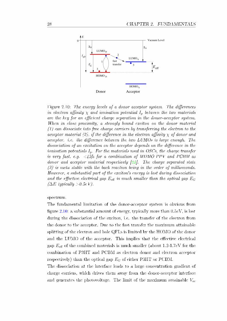
28 CHAPTER 2. FUNDAMENTALS
LUMOA
HOMO D
LUMO D
fast
transfer
HOMOA
χD χA
0
1
2
3
3
Donor
Vacuum Level
Acceptor
Eeff
EG
IpD
E
Figure 2.10: The energy levels of a donor-acceptor system. The dierencesin electron anity χ and ionisation potential Ip between the two materialsare the key for an ecient charge separation in the donor-acceptor system.When in close proximity, a strongly bound exciton on the donor material(1) can dissociate into free charge carriers by transferring the electron to theacceptor material (2), if the dierence in the electron anity χ of donor andacceptor. i.e. the dierence between the two LUMOs is large enough. Thedissociation of an excitation on the acceptor depends on the dierence in theionisation potentials Ip. For the materials used in OSCs, the charge transferis very fast, e.g. <45fs for a combination of MDMO-PPV and PCBM asdonor and acceptor material respectively [21]. The charge separated state(3) is meta stable with the back reaction being in the order of milliseconds.However, a substantial part of the exciton's energy is lost during dissociationand the eective electrical gap Eeff is much smaller than the optical gap EG
(∆E typically >0.5eV).
spectrum.
The fundamental limitation of the donor-acceptor system is obvious from
gure 2.10: a substantial amount of energy, typically more than 0.5eV, is lost
during the dissociation of the exciton, i.e. the transfer of the electron from
the donor to the acceptor. Due to the fast transfer the maximum attainable
splitting of the electron and hole QFLs is limited by the HOMO of the donor
and the LUMO of the acceptor. This implies that the eective electrical
gap Eeff of the combined materials is much smaller (about 1.2-1.7eV for the
combination of P3HT and PCBM as electron donor and electron acceptor
respectively) than the optical gap EG of either P3HT or PCBM.
The dissociation at the interface leads to a large concentration gradient of
charge carriers, which drives them away from the donor-acceptor interface
and generates the photovoltage. The limit of the maximum attainable Voc
2.3. THE BULK HETEROJUNCTION SOLAR CELL 29
is thus given by Eeff rather than by the dierence in workfunctions of the
contacts [13]. The Eeff can be changed by using an acceptor or donor with
dierent LUMO or HOMO respectively. Subsequently changes in Voc are
observed [20].
Using dierent donor-acceptor materials raises the question of how big the
energy dierence of the levels involved in the transfer has to be in order to
extract the maximum power [22]. This question has not been answered so
far, because the details of the charge transfer are not completely understood
yet and will strongly depend on the involved materials.
2.3.2 The Bulk Heterojunction
The rst OSCs were realised as bi-layer devices of donor and acceptor. They
reached a power conversion eciencies of around 1% [23]. Excitons are gener-
ated throughout the device, however, they typically diuse only about 10nm
(MDMO-PPV, [24]) before decaying. Hence only excitons created within this
distance of the planar interface between donor and acceptor material split
eectively into free charge carriers. This considerable limitation was solved
by blending donor and acceptor material which by virtue of the mesoscopic
morphology can create a large interfacial area between donor and acceptor
on length scales comparable to the exciton diusion length [25]. The result-
ing interpenetrating donor-acceptor network is called a bulk heterojunction,
because the heterojunction is distributed throughout the photovoltaic active
volume. It is an ongoing research challenge to realise the optimal morphol-
ogy in which the phase separation is small enough to have ecient charge
carrier separation while still to ensure that there are continuous pathways,
i.e. percolation paths, to the corresponding contact.
The OSC structure shown in gure 2.11 is currently the most widely inves-
tigated structure and will be used as model system for describing the key
features of organic bulk heterojunction solar cells.
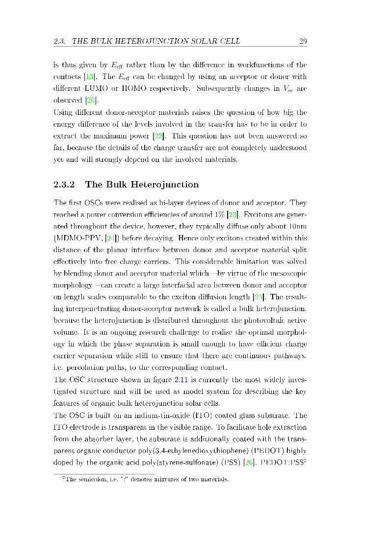
The OSC is built on an indium-tin-oxide (ITO) coated glass substrate. The
ITO electrode is transparent in the visible range. To facilitate hole extraction
from the absorber layer, the substrate is additionally coated with the trans-
parent organic conductor poly(3,4-ethylenedioxythiophene) (PEDOT) highly
doped by the organic acid poly(styrene-sulfonate) (PSS) [26]. PEDOT:PSS2
2The semicolon, i.e. : denotes mixtures of two materials.
30 CHAPTER 2. FUNDAMENTALS
indium−tin−oxide (transparent), approx. 120nm PEDOT:PSS (transparent), 40−60nmpolymer:PCBM absorber layer, 80−300nm
reflective aluminium electrode, 80−150nm
glass substrate, 1.1mm
Figure 2.11: The typical layer structure of a polymer-PCBM OSC. A glasscoated with indium-tin-oxide (ITO) serves as substrate. A thin PEDOT:PSSlayer on top of the ITO, acts as anode for the polymer:PCBM layer, whichwill be called absorber layer throughout this work. The cathode is realisedthrough an evaporated aluminium layer. Both PEDOT:PSS and absorberlayer are spin-coated from solution. The illumination is through the substrate.
serves as the hole contact and its chemical structure is shown in gure 2.16.
The photovoltaic active absorber layer, consisting of a polymer:PCBM blend
is applied from solution. Finally, the electron contact of the absorber layer is
realised by evaporating an 80-150nm thick, highly reecting aluminium (Al)
electrode onto the absorber. Sometimes a 0.6nm thick lithiumuoride (LiF)
layer is being evaporated between absorber layer and aluminium cathode,
because it is claimed that this improves the OSC performance [12, p. 217].
The whole OSC production process is described in detail in chapter 3.
The absorption of light takes primarily place in the absorber layer. Various
semiconducting polymers have been used, of which the more common ones are
PPV-derivatives and P3HT, being introduced in gure 2.9. However, with
the currently used organic materials the overlap between their absorption
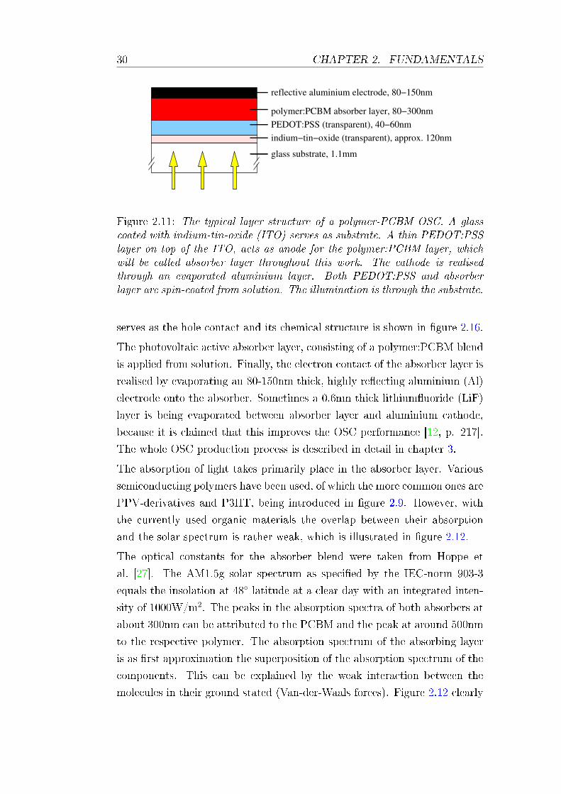
and the solar spectrum is rather weak, which is illustrated in gure 2.12.
The optical constants for the absorber blend were taken from Hoppe et
al. [27]. The AM1.5g solar spectrum as specied by the IEC-norm 903-3
equals the insolation at 48 latitude at a clear day with an integrated inten-
sity of 1000W/m2. The peaks in the absorption spectra of both absorbers at
about 300nm can be attributed to the PCBM and the peak at around 500nm
to the respective polymer. The absorption spectrum of the absorbing layer
is as rst approximation the superposition of the absorption spectrum of the
components. This can be explained by the weak interaction between the
molecules in their ground stated (Van-der-Waals forces). Figure 2.12 clearly
2.3. THE BULK HETEROJUNCTION SOLAR CELL 31
300 400 500 600 700 800 900 1000Wavelength / nm
0
0.5
1
1.5
2
Abs
orpt
ion
(mea
sure
d in
tran
smis
sion
) / a
rb. u
nits
0
0.5
1
1.5
2
djE/d
λ /
W/(
m2 n
m)
AM1.5gMDMO-PPV:PCBM 1:4P3HT:PCBM 1:2
Tue Aug 8 14:57:15 2006
Figure 2.12: The absorption spectrum for OSCs with a MDMO-PPV:PCBM(1:4 by weight) and P3HT:PCBM (1:2 by weight) as absorber layer as mea-sured in transmission (data taken from [27]). For comparison, the AM1.5gspectrum is shown on the right axis. Due to an additional absorption shoul-der in the red spectral region P3HT can harvest more of the sun light thanMDMO-PPV.
shows that the absorption of the photovoltaic active materials covers only a
small part of the solar spectrum. MDMO-PPV, the polymer being previously
at the focus of research, has been replaced by P3HT in the last two years,
because the latter absorbs further into the red of the solar spectrum. The
characteristic shoulder at 600nm in the P3HT absorption spectrum is caused
by an improved ordering of the P3HT chains [28].
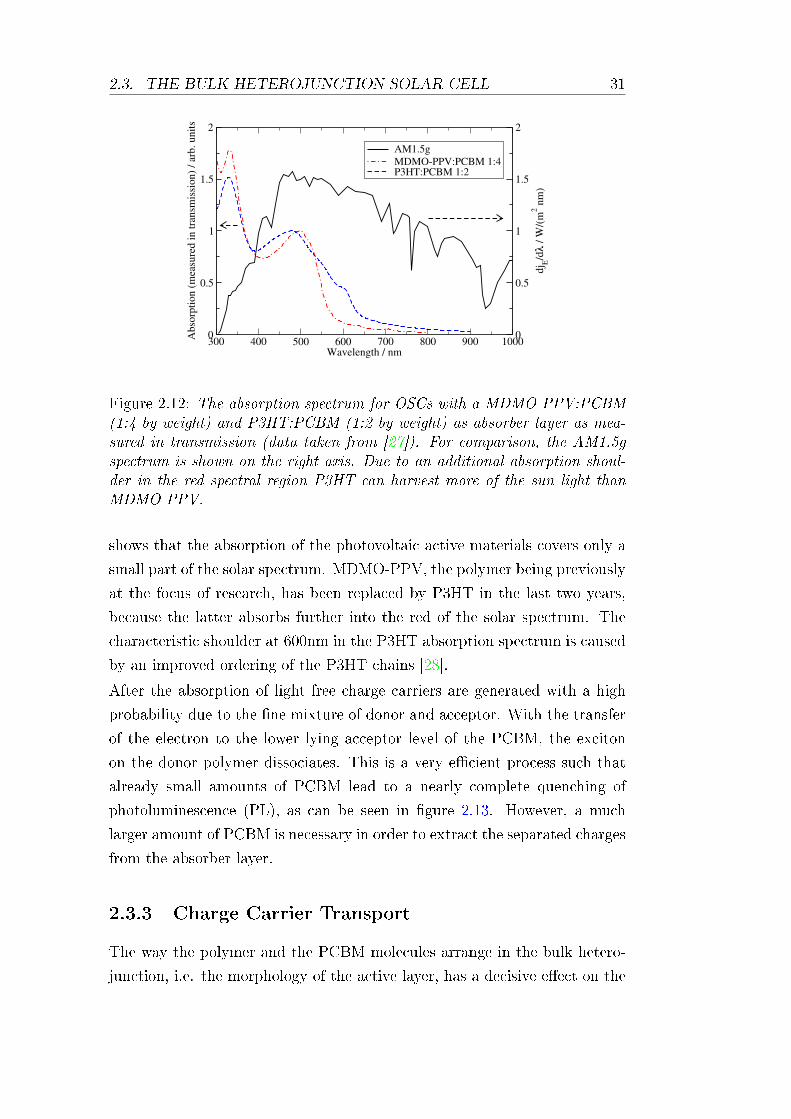
After the absorption of light free charge carriers are generated with a high
probability due to the ne mixture of donor and acceptor. With the transfer
of the electron to the lower lying acceptor level of the PCBM, the exciton
on the donor polymer dissociates. This is a very ecient process such that
already small amounts of PCBM lead to a nearly complete quenching of
photoluminescence (PL), as can be seen in gure 2.13. However, a much
larger amount of PCBM is necessary in order to extract the separated charges
from the absorber layer.
2.3.3 Charge Carrier Transport
The way the polymer and the PCBM molecules arrange in the bulk hetero-
junction, i.e. the morphology of the active layer, has a decisive eect on the
32 CHAPTER 2. FUNDAMENTALS
0.1 1 10 100Concentration of PCBM / mol %
0
0.2
0.4
0.6
0.8
1
Phot
olum
ines
cenc
e In
tens
ity /
arb.
uni
ts
0
0.2
0.4
0.6
0.8
1
I sc /
arb.
uni
ts
Short Circuit Current IscPhotoluminescence
Fri Nov 24 22:31:39 2006
Figure 2.13: Photoluminescence (PL) and short circuit current Isc are shownas function of the molar PCBM concentration in a polymer matrix of MDMO-PPV (redrawn after [12, p. 166]). Already at a PCBM concentration of1mol%, the PL is signicantly quenched. However, PCBM concentrations ofmore than 17mol% are necessary to observe the onset of Isc, which saturatesfor more than 30mol%PCBM.
charge carrier transport and thus on the OSC performance. The two com-
ponents are not mixable (but soluble in a common solvent) and the phase
separation has to be similar size as the exciton diusion length (about 10nm)
for ecient exciton dissociation. The low charge carrier mobilities also limit
the maximum device thickness.
When mixing MDMO-PPV and PCBM, nearly all excitons already dissociate
at 1mol% PCBM concentration, as can be inferred from the extinction of
the polymer's photoluminescence. However, as gure 2.13 shows, a much
higher PCBM concentration (about 20mol%) is necessary for sucient charge
transport to the electrode. For MDMO-PPV it has been shown that the
maximum eciency is reached for PCBM concentrations of up to 80mol%,
depending on the thickness of the absorber. Eciencies of around 3% are
reported in literature. However, it is apparently not the electron mobility,
which requires such a high PCBM concentration, but the hole mobility in
MDMO-PPV, which benets from the high PCBM concentration [29]. This
leads to two limitations of the MDMO-PPV:PCBM OSC: PCBM is hardly
absorbing the solar spectrum and the morphology is not thermodynamically
stable, i.e. the PCBM has the tendency to form clusters, which can exceed
the exciton diusion length [30].
P3HT:PCBM based OSCs require much less PCBM and an η approach-
2.3. THE BULK HETEROJUNCTION SOLAR CELL 33
ing 5% has been reported for concentrations between 1:0.6-0.8 polymer to
PCBM [31]. P3HT can be made to crystallise in the absorber layer, improv-
ing the hole mobilities by nearly three order of magnitude, reaching values
close to the ones obtained for pristine spin-coated lms (about 10−8Vs/cm2).
Still µh is at least one order of magnitude lower than the electron mobility
in the bulk [14]. Modication of the morphology on the nanometre scale
is achieved by a heat treatment of the OSC after production, often with
temperatures up to 150C. During the heat treatment, the structure of the
morphology, which has been frozen when the solvent evaporated during spin-
coating, can relax to a energetically more favourable conguration. P3HT
with a high regioregularity can form nano- or even micro-crystalline domains
in the absorber layer, which lead to the observed increase µh. Much re-
search is currently focussed on optimising the morphology and a thermal
post-treatment step has become a standard process for P3HT:PCBM based
OSCs.
An additional issue which has to be considered when describing the transport
in a bulk heterojunction are the percolation paths, i.e. whether there is a
continuous path of the same material to the respective electrode. Once the
exciton has dissociated the charge carriers the hole on the polymer and the
electron on the PCBM have to nd a way towards their respective electrode.
Depending on the phase separation, i.e. the degree of mixing of polymer and
PCBM, there are e.g. regions of the polymer which have direct contact to
no electrode or only the cathode. However, the phase separation itself is in
the most cases not directly accessible. Its dimensions require atomic force
microscopy (AFM) and it is often not possible to infer from the AFM surface
the morphology in the bulk.
2.3.4 Charge Carrier Extraction at the Contacts
As described in section 2.1.3, ideal contacts need to satisfy the following
two requirements: (1) they have to be semipermeable only to the respective
charge carriers and (2) have to contact the corresponding transport levels.
Then the chemical potential energy in the semiconductor can be converted
without loss into electrical energy in the external circuit. However, real
contacts in solar cells do generally not meet both requirements and the solar
cell performance therefore depends signicantly on the choice of electrodes.
34 CHAPTER 2. FUNDAMENTALS
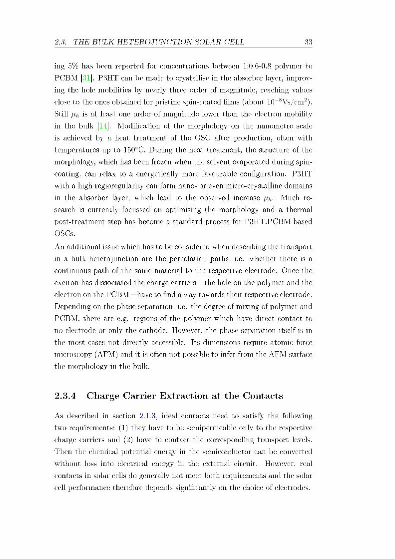
When the contact between a metal and a semiconductor is formed, charge
carriers are transferred across the interface until the Fermi level of the metal
and semiconductor align at the interface and throughout the combined sys-
tem. The simple picture in gure 2.14 shows a Schottky contact formation,
i.e. between a semiconductor, here p-type, and a metal. In this example,
electrons ow from the metal into the semiconductor charging it negatively.
The redistribution of charges due to equilibration of the Fermi levels creates
a potential dierence leading to a bending of the bands inside the semicon-
ductor, which eventually stops the transfer of further charges through the
interface once the Fermi levels are equal. The energy barrier for injecting
Depletion
Region
Φm2
Φm2
0E
Vacuum Level
−
−
EF
EV
EC
EC
EF
EV B
eVd
φ
Figure 2.14: The energy diagram of a p-type semiconductor and a metalprior to contact formation (left) and after contact formation (right). Uponcontact formation, charges are transferred across the interface until the Fermilevels of on both sides of the contact are equal. The electric eld caused bythe transferred charges leads to a bending of the electronic bands inside thesemiconductor, the region of which is called depletion region. The vacuumlevel is displaced by eVd and a barrier φB forms at the interface.
holes into the metal in this simple picture is then given as
φB = EV + Φm2 (2.17)
The region of band bending is called the depletion region. For organic
semiconductors the depletion region can extend, depending on the material,
through the whole absorber layer [32].
This simple picture neglects several important issues and there is much re-
search going on with regard to the properties of metal-organic interfaces. A
detailed description of the physical processes involved at the interfaces be-
tween metals and organic semiconductors is beyond the scope of this work.
2.3. THE BULK HETEROJUNCTION SOLAR CELL 35
A very important factor is the incommensurability of the crystal structures
(crystalline vs. amorphous) of the interfacing materials. Further factors in-
uencing the interface formation are, e.g. the wave function hybridisation,
charge transfer and chemical reactions. The interested reader is referred to
the reviews in references [33, 34]. Contact models for contacts between inor-
ganic semiconductors and metals have to be used carefully and be viewed in
the light of the fundamental dierences between organic and inorganic semi-
conductors (see table 2.1). In the following sections, only the main issues
are summarised. Furthermore, it is described how the performance of OSCs
depends on the choice of electrode materials.
The formation of the interfaces depends on:
• the energy levels, crystal structure, surface morphology, molecular struc-
ture and alignment at interface,
• the sequence in which the materials are deposited (organic-metal or
metal-organic),
• the method of deposition of the materials and its parameters (evapo-
ration or coating from solution),
• the workfunction of the two materials and possible dierence in vacuum
levels.
The contacted bulk heterojunction solar cell has three planar interfaces be-
tween dierent materials (gure 2.11), leading to the energy diagram shown
in gure 2.15. The properties of these interfaces will be discussed in the
following.
The Polymeric Anode
The most commonly used anode is the organic conductor PEDOT:PSS, sup-
ported by the metal oxide ITO, leading to two interfaces for the charge
carrier: ITO|PEDOT:PSS3 and PEDOT:PSS|Absorber.
ITO is used as transparent electrode in many applications, e.g. at panel
displays, where good electrical conductivity as well as high optical trans-
parency in the visible region and processability are paramount. ITO alone
could serve as anode in OSCs or OLEDs, but it has been shown that an
3The vertical dash, i.e. |, denotes the planar interface between two materials
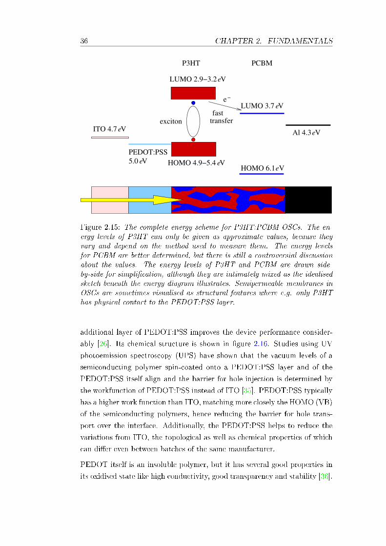
36 CHAPTER 2. FUNDAMENTALS
e−
transferexcitonfast
P3HT
PEDOT:PSS
PCBM
5.0 Ve
ITO 4.7 Ve
eLUMO 2.9−3.2 V
Al 4.3 Ve
HOMO 4.9−5.4 VeHOMO 6.1 Ve
LUMO 3.7 Ve
Figure 2.15: The complete energy scheme for P3HT:PCBM OSCs. The en-ergy levels of P3HT can only be given as approximate values, because theyvary and depend on the method used to measure them. The energy levelsfor PCBM are better determined, but there is still a controversial discussionabout the values. The energy levels of P3HT and PCBM are drawn side-by-side for simplication, although they are intimately mixed as the idealisedsketch beneath the energy diagram illustrates. Semipermeable membranes inOSCs are sometimes visualised as structural features where e.g. only P3HThas physical contact to the PEDOT:PSS layer.
additional layer of PEDOT:PSS improves the device performance consider-
ably [26]. Its chemical structure is shown in gure 2.16. Studies using UV
photoemission spectroscopy (UPS) have shown that the vacuum levels of a
semiconducting polymer spin-coated onto a PEDOT:PSS layer and of the
PEDOT:PSS itself align and the barrier for hole injection is determined by
the workfunction of PEDOT:PSS instead of ITO [35]. PEDOT:PSS typically
has a higher work function than ITO, matching more closely the HOMO (VB)
of the semiconducting polymers, hence reducing the barrier for hole trans-
port over the interface. Additionally, the PEDOT:PSS helps to reduce the
variations from ITO, the topological as well as chemical properties of which
can dier even between batches of the same manufacturer.
PEDOT itself is an insoluble polymer, but it has several good properties in
its oxidised state like high conductivity, good transparency and stability [36].
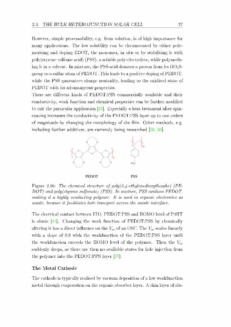
2.3. THE BULK HETEROJUNCTION SOLAR CELL 37
However, simple processability, e.g. from solution, is of high importance for
many applications. The low solubility can be circumvented by either poly-
merising and doping EDOT, the monomer, in situ or by stabilising it with
poly(styrene sulfonic acid) (PSS), a soluble poly-electrolyte, while polymeris-
ing it in a solvent. In mixture, the PSS-acid donates a proton from its HO3S-
group to a sulfur atom of PEDOT. This leads to a positive doping of PEDOT,
while the PSS guarantees charge neutrality, leading to the oxidised state of
PEDOT with its advantageous properties.
There are dierent kinds of PEDOT:PSS commercially available and their
conductivity, work function and chemical properties can be further modied
to suit the particular application [37]. Especially a heat treatment after spin-
coating increases the conductivity of the PEDOT:PSS layer up to two orders
of magnitude by changing the morphology of the lm. Other methods, e.g.
including further additives, are currently being researched [36, 38].
S
S
S
O O
O O
O O
n
HO3S
m
PEDOT PSS
Figure 2.16: The chemical structure of poly(3,4-ethylenedioxythiophe) (PE-DOT) and poly(styrene-sulfonate) (PSS). In mixture, PSS oxidises PEDOT,making it a highly conducting polymer. It is used in organic electronics asanode, because it facilitates hole transport across the anode interface.
The electrical contact between ITO, PEDOT:PSS and HOMO level of P3HT
is ohmic [14]. Changing the work function of PEDOT:PSS by chemically
altering it has a direct inuence on the Voc of an OSC. The Voc scales linearly
with a slope of 0.8 with the workfunction of the PEDOT:PSS layer until
the workfunction exceeds the HOMO level of the polymer. Then the Voc
suddenly drops, as there are then no available states for hole injection from
the polymer into the PEDOT:PPS layer [37].
The Metal Cathode
The cathode is typically realised by vacuum deposition of a low workfunction
metal through evaporation on the organic absorber layer. A thin layer of alu-
38 CHAPTER 2. FUNDAMENTALS
minium is the most common cathode, but other materials have been tested,
e.g. Ca|Ag. Still, the interface formation between the absorber layer and the
evaporated metal cathode has up to now not been accurately described.
For inorganic semiconductors, the contact formation to metals is well re-
searched. However, the contact between organic semiconductors and metals
has on the one hand strong bonds in the metal and weak van-der-Waals bonds
in the organic semiconductor. Additionally, their structures are incommen-
surate. In the metal there are very many charge carriers and the transport is
band-like. Organic semiconductor have very few charge carriers and a trans-
port mechanism which is dominated by thermally assisted hopping. These
dierences make direct transfer of contact models from the inorganic picture
to contact between metals and organic materials not possible. The details of
the ongoing debate on how the interface properties form are however beyond
the scope of this work.
The dependence of Voc on the metal workfunction has been investigated by
Brabec et al. for the MDMO-PPV:PCBM combination [20], who also deter-
mined for comparison the inuence of the acceptor strength of the electron
acceptor (fullerene). Whereas the Voc exhibited only a weak dependence
on the change in workfunction, is was directly proportional to the accep-
tor strength of the fullerene, suggesting that the dierence in energy levels
(HOMO donor to LUMO acceptor) is more relevant to Voc than the metal
workfunctions.
Mihailetchi at al. [39] showed for another PPV-derivative that depending on
the used metal for the cathode, an ohmic or non-ohmic contact is realised
at the interface to the organic semiconductor, and calculated the associated
barriers and voltage drops. They claim that in the case of non-ohmic contacts
the Voc is only determined by the workfunction dierence of the contacting
metal as expected from the metal-insulator-metal picture [7]. In the ohmic
case, however, the Voc is governed by the dierence in HOMO and LUMO
level of donor and acceptor respectively in agreement with the ndings of
Brabec et al.. Here, the workfunctions of the cathode is pinned close to the
LUMO of the acceptor and band bending leads to a voltage drop of typically
0.2V across the interface. The term pinning is used in OSCs in a dierent
context than for inorganic semiconductors.
2.3. THE BULK HETEROJUNCTION SOLAR CELL 39
2.3.5 Loss Mechanisms
Just like the charge transfer at the interfaces between organic and inorganic
materials is an active eld of research, so are charge recombination processes
both in the bulk of the absorber and at the interfaces. The assessment of the
optical losses is important in quantifying the number of absorbed photons in
the photovoltaic active absorber layer. With a charge separation of the exci-
ton faster than picoseconds in the bulk heterojunction, the direct radiative
recombination of the exciton is unlikely as evident from the quenching of the
photoluminescence [21]. Thus, it can be assumed that every photogenerated
exciton dissociates. However, the free charge carriers still can recombine be-
fore being extracted at the contacts and the current understanding of the
mechanisms is presented here.
Interface Recombination
Due to the dierent structure of metal (crystalline) and absorber (amor-
phous) and the continuous distribution of electronic states in the metal, the
presence of states in the energy gap of the semiconductor at the interface is
very likely. These states facilitate non-radiative charge recombination and
losses can be high, as known from silicon solar cells. There the contact
area is reduced as much as possible in order to avoid interface recombination
losses or a barrier for the opposite charge carrier is created by a local eld.
However, no quantitative studies on the eect of interface recombination in
organic semiconductors have been published to the best of my knowledge.
Bulk Recombination
The large interface area between donor and acceptor in the bulk heterojunc-
tion is necessary for a very ecient separation of photogenerated excitons.
However, the large interface area and the intimate mixing also suggest the
possibility of high recombination in the bulk, because donor and acceptor are
spatially not well separated.
Studies with transient absorption spectroscopy on MDMO-PPV:PCBM lay-
ers have shown two dierent decay regimes [40, 41] of the photogenerated
hole on MDMO-PPV, which are both associated with the recombination of
hole on the polymer and an electron on the PCBM. They detected a fast
regime with decay times <20ns, which depended strongly on the intensity of
40 CHAPTER 2. FUNDAMENTALS
the excitation pulse, and a slow regime with decay times between 300ns and
10ms, which quickly saturates with excitation density. The long-lived holes
are thought to be trapped in localised states above the transport edge of
the polymer HOMO. At pulse intensities comparable to solar irradiation, the
slow regime was found to be dominating. It decays with a power law and the
process is thermally activated. At high intensities, these localised trap levels
get saturated and further polarons are in states where transport is easier. It
is interesting to note that the decay between 300ns and 1ms is primarily as-
sociated with decay in bulk of the polymer and is independent of the PCBM
concentration apart from time scales >1ms. Their conclusion is that at solar
intensities, if mobility of untrapped holes is suciently high (>10−3cm2/Vs),
charge recombination is suciently slow and does not inuence the short
circuit current.
If the mobility is lower or other recombination mechanisms come into play,
the dependence of the photocurrent on the incident light intensity is not
linear any more. Thus intensity dependent measurements can be used to
assess recombination mechanisms in solar cells. In the ideal case, the photo-
generated current should scale linearly with the incident light intensity Pill.
However, in the real case, this behaviour often deviates from the linear rela-
tion. Assuming a power law relation between photogenerated current I the
relation can be written as
I(Pill) ∝ Pαill, (2.18)
where α is the scaling coecient, i.e. the slope of I versus Pill in a loglog plot.
The scaling coecient can give information on the dominant recombination
mechanism. If the recombination is bimolecular, i.e. depends on the densities
of free holes and electrons, α ≈ 0.5. For monomolecular, e.g. trap assisted
recombination processes, α is expected to be 1.
Optical Losses
Optical losses in the OSC set an upper limit on the number of charges, which
can be generated under illumination. Reections at the interfaces and ab-
sorption of photons in layers, which are not photovoltaic active, reduce the
number of photons available for absorption in the absorber layer (see g-
ure 2.11). The main reections occur at the air-glass interface and at the
metal electrode. The latter reection leads to the creation of an optical
2.4. OSC MODELLING 41
interference pattern, because the thickness of the layer structures is in the
same order at the wavelength of the incident light. Thus interference ef-
fects have a crucial eect on the absorption and any optical treatment has
to be carried out coherently. The interesting region for the current materi-
als (P3HT:PCBM) is between 300nm and 800nm. Optical simulations have
shown that below 350nm most of the light is absorbed in the glass [42]. How-
ever, the AM1.5g photon ux is very small in this interval. Up to 550nm
most photons are absorbed in the photovoltaic layer. At higher wavelengths,
the absorption of the photovoltaic active materials decreases (see gure 2.12)
and more photons are absorbed in PEDOT:PSS layer and the cathode.
2.4 OSC Modelling
Several attempts in modelling the current-voltage behaviour of OSCs have
been made. There are two main approaches: microscopic models starting
from transport, continuity and Poisson equations and equivalent circuit mod-
els built on basic electrical units like resistors and diodes. Both approaches
will briey be presented here.
2.4.1 Microscopic Models
The microscopic models proposed for OSCs are all based on the metal-
insulator-metal picture [43, 44, 45, 46]. The interpenetrating network of
donor and acceptor in the absorber layer is here replaced by one virtual semi-
conductor, which combines properties of both materials. Table 2.2 briey
summarises its typical properties. One justication for this approach is that
the dissociation of the photogenerated excitons is a femtosecond reaction and
the free charge carriers end up on dierent materials [25]. This virtual semi-
conductor is contacted with cathode and anode at the respective energy. For
this system, the standard equations for describing the transport through a
semiconductor are solved self consistently. Usually only the direction normal
to the absorber layer, i.e. only one spatial dimension, is considered, because
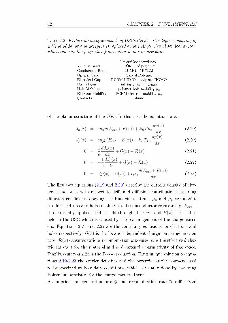
42 CHAPTER 2. FUNDAMENTALS
Table 2.2: In the microscopic models of OSCs the absorber layer consisting ofa blend of donor and acceptor is replaced by one single virtual semiconductor,which inherits the properties from either donor or acceptor.
Virtual SemiconductorValence Band HOMO of polymerConduction Band LUMO of PCBMOptical Gap Gap of PolymerElectrical Gap PCBM LUMO - polymer HOMOFermi Level intrinsic, i.e. mid-gapHole Mobility polymer hole mobility µp
Electron Mobility PCBM electron mobility µn
Contacts ohmic
of the planar structure of the OSC. In this case the equations are:
Jn(x) = eµnn(Eext + E(x)) + kBTµndn(x)
dx(2.19)
Jp(x) = eµpp(Eext + E(x))− kBTµpdp(x)
dx(2.20)
0 =1
e
dJn(x)
dx+ G(x)−R(x) (2.21)
0 = −1
e
dJp(x)
dx+ G(x)−R(x) (2.22)
0 = e(p(x)− n(x)) + εrεod(Eext + E(x))
dx(2.23)
The rst two equations (2.19 and 2.20) describe the current density of elec-
trons and holes with respect to drift and diusion contributions assuming
diusion coecients obeying the Einstein relation. µn and µp are mobili-
ties for electrons and holes in the virtual semiconductor respectively. Eext is
the externally applied electric eld through the OSC and E(x) the electric
eld in the OSC which is caused by the rearrangement of the charge carri-
ers. Equations 2.21 and 2.22 are the continuity equations for electrons and
holes respectively. G(x) is the location dependent charge carrier generation
rate. R(x) captures various recombination processes, εr is the eective dielec-
tric constant for the material and ε0 denotes the permittivity of free space.
Finally, equation 2.23 is the Poisson equation. For a unique solution to equa-
tions 2.19-2.23 the carrier densities and the potential at the contacts need
to be specied as boundary conditions, which is usually done by assuming
Boltzmann statistics for the charge carriers there.
Assumptions on generation rate G and recombination rate R dier from
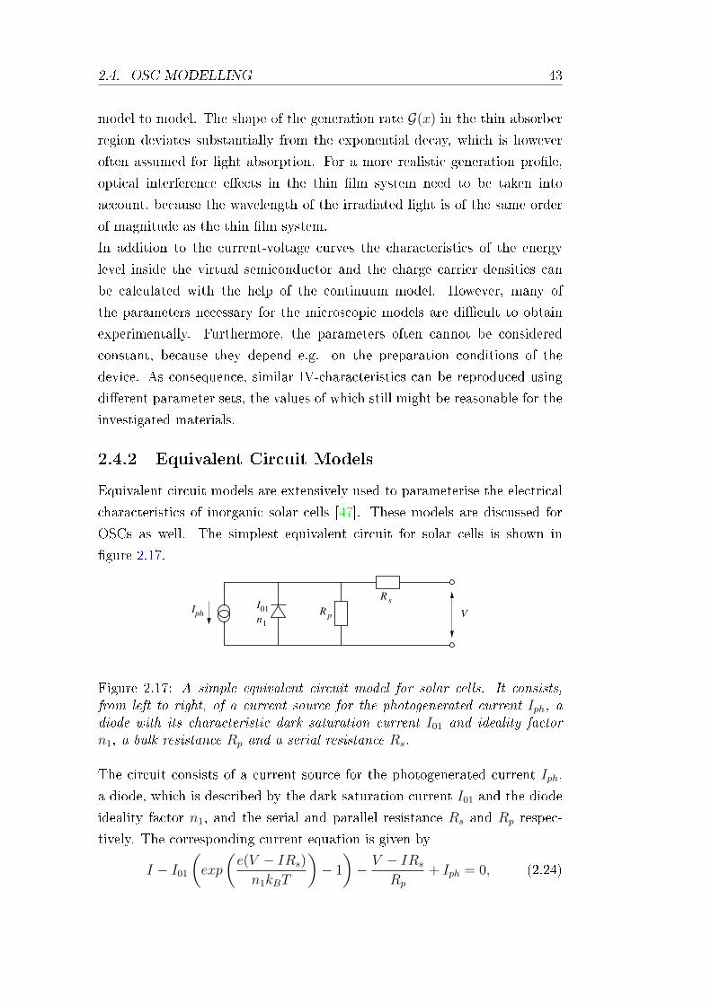
2.4. OSC MODELLING 43
model to model. The shape of the generation rate G(x) in the thin absorber
region deviates substantially from the exponential decay, which is however
often assumed for light absorption. For a more realistic generation prole,
optical interference eects in the thin lm system need to be taken into
account, because the wavelength of the irradiated light is of the same order
of magnitude as the thin lm system.
In addition to the current-voltage curves the characteristics of the energy
level inside the virtual semiconductor and the charge carrier densities can
be calculated with the help of the continuum model. However, many of
the parameters necessary for the microscopic models are dicult to obtain
experimentally. Furthermore, the parameters often cannot be considered
constant, because they depend e.g. on the preparation conditions of the
device. As consequence, similar IV-characteristics can be reproduced using
dierent parameter sets, the values of which still might be reasonable for the
investigated materials.
2.4.2 Equivalent Circuit Models
Equivalent circuit models are extensively used to parameterise the electrical
characteristics of inorganic solar cells [47]. These models are discussed for
OSCs as well. The simplest equivalent circuit for solar cells is shown in
gure 2.17.
VIph
01I
1nR
p
Rs
Figure 2.17: A simple equivalent circuit model for solar cells. It consists,from left to right, of a current source for the photogenerated current Iph, adiode with its characteristic dark saturation current I01 and ideality factorn1, a bulk resistance Rp and a serial resistance Rs.
The circuit consists of a current source for the photogenerated current Iph,
a diode, which is described by the dark saturation current I01 and the diode
ideality factor n1, and the serial and parallel resistance Rs and Rp respec-
tively. The corresponding current equation is given by
I − I01
(exp
(e(V − IRs)
n1kBT
)− 1
)− V − IRs
Rp
+ Iph = 0, (2.24)
44 CHAPTER 2. FUNDAMENTALS
where kB is the Boltzmann constant, T the temperature of the device, V the
externally applied bias voltage.
Rp takes the leakage current through the solar cell into account. Rs has
contributions from the bulk and the interface, which can be distinguished by
carefully varying the absorber layer thickness [48]. In the ideal case, Rs = 0,
Rp = ∞ and equation 2.24 can easily be solved. In this simple picture,
the illuminated IV-curve equals the dark IV-curve just being shifted by the
photogenerated current. If Rs 6= 0, the equation has to be solved numerically.
Using a set of sensible parameters I01, n1, T , Rs, Rp, Iph leads to typical
IV-characteristics.
Equivalent circuit models have been applied to OSCs and attempts have been
made to extend the simple model above in order to account for the deviations
seen in OSCs. The extension of the simple model is said to be necessary to
account for the bias dependence of the photocurrent Iph, the illumination de-
pendent dark saturation current I01 and the illumination dependent parallel
resistance Rp.
Schilinsky et al. proposed a modication to the simple diode model to take
the bias dependence of the photocurrent and the illumination dependence of
Rp in a P3HT:PCBM bulk heterojunction solar cell into account [49]. With
the assumption that the photogenerated charges are only driven by the elec-
tric eld, the photocurrent changes sign when the external eld compensates
the built-in eld. Their modication is similar to what is used in models for
amorphous silicon [50, 51]. The illumination dependence of Rp is in their
model explained by separating Rp into Rp(dark), the parallel resistance in
the dark, and Rp(ill), an intensity dependent term. Rp(ill) is often called
photo-shunt, because of its intensity dependence. Its physical origin and
meaning is not clear yet.
Yoo et al. try to included the seen deviation from the single diode model
by adding a second, intensity dependent diode parallel to the rst one [52].
They also added a light intensity dependent second Rp, which is analogous
to the model proposed by Schilinsky. With the help of this model, they
successfully determined the intensity dependence of the model parameters,
but do not discuss the physical origin and meaning of these parameters. In
addition to produce adequate ts, this is currently the main problem of the
equivalent circuit models, i.e. establishing a link between the t parameters
and a physical explanation.
Chapter 3
OSC Production
This chapter introduces the organic solar cells (OSCs) used in this work and
describes their production process at a laboratory scale. Each production
step is presented with its main parameters, which are recorded for the data
analysis. As far as there are standard procedures, these will be summarised.
The description is detailed, because the analysis of the interdependence be-
tween OSC production and OSC properties obtained during characterisation
are at the focus of chapter 6.
3.1 Standard OSC Layer Structure
The many dierent types of organic solar cells described in literature result
from the large variety of available organic semiconductors and production
technologies. They range from the evaporation of organic layers from very
pure oligomers onto suitable substrates [53, 54] to coating of substrates with
organic semiconductors from solution [25, 55, 56]. The OSCs investigated
here are of the latter type and this section introduces what will be the stan-
dard OSC used in this work.
The layer structure of the standard OSC is shown in gure 3.1. It has already
been used as example when describing the OSC fundamentals in chapter 2.
Its main features are quickly summarised here again, specifying the materials
used in this work.
The OSC is built on an indium-tin-oxide (ITO)-coated glass substrate. The
ITO supports the conductivity of a thin, transparent layer of poly(3,4-ethylene-
dioxythiophene) (PEDOT), which is doped with poly(styrene-sulfonate) (PSS)
and spin-coated on top of the ITO. The PEDOT:PSS layer has proven to fa-
cilitate the contact to the absorber layer and the hole transport across this
45
46 CHAPTER 3. OSC PRODUCTION
indium−tin−oxide (transparent), approx. 120nm PEDOT:PSS (transparent), 40−60nmpolymer:PCBM absorber layer, 80−300nm
reflective aluminium electrode, 80−150nm
glass substrate, 1.1mm
Figure 3.1: The layer structure of the standard OSC used in this work. It isbased on an ITO-coated glass substrate, on which the other layers are sub-sequently added during the production process. The polymer:PCBM absorberlayer is the photovoltaic active region. The illumination is through the glasssubstrate and transparent ITO|PEDOT:PSS anode, i.e. here from below.
interface [26]. The photovoltaic active absorber layer consists of a blend of
an electron donating polymer and the electron accepting fullerene deriva-
tive, which is applied by spin-coating as well. The materials used here
are the polymer P3HT (poly(3-hexylthiophene)) and the electron acceptor
PCBM (1-(3-methoxycarbonyl)-propyl-1-1-phenyl-(6,6)C61). Typical ratios
of P3HT:PCBM are between 1:0.5 and 1:2 by weight. The thickness of the
absorber layer is with 100-300nm sucient for ecient light absorption in
their absorbing regime due to the high absorption coecients of the used
materials. The cathode is realised through an evaporated aluminium elec-
trode. The illumination of the OSC is from the substrate side through the
ITO and PEDOT:PSS layer.
3.2 OSC Production Process
The production process investigated in this work can be described as sequence
of dierent process groups, which consist generally of several process steps.
An overview is shown in gure 3.2. The process groups are shown in boxes
and the name of the outcome of each group is shown in hexagons. The mea-
surements (yellow ellipse) are shown for completeness and their correspond-
ing details are described in chapter 4. An illustrative way of representing the
production process of the standard OSC is shown on the left in gure 3.2,
where the formation of the layer structure of the substrates after each process
group is depicted. One important point of the production process is that for
spin-coating steps, the substrates can only be handled sequentially, whereas
3.2. OSC PRODUCTION PROCESS 47
Table 3.1: The general parameters recorded for every production step in ad-dition to the process specic parameters. They are all mandatory, apart fromthe comment, which can be used to note details otherwise dicult to record.
Parameter Symbol StandardSubstrate e.g. S 123Timestamp YYYY-MM-DD HH:MMLocation process dependentResearcher login name(optional: Comment)
all other allow the processing of more than one substrate at a time (batch).
This is depicted on the right in gure 3.2 and leads to dierent time inter-
vals between steps for the substrates within one batch when moving from a
sequential to a batch process step.
A detailed structuring and understanding of the OSC production process is
necessary to allow its standardisation and adequate mapping to an electronic
protocol (see section 5.2.2). This includes the denition of a well dened set
of production parameters, which needs to be recorded for every OSC made
in order to allow comparative OSC production and subsequent testing.
Using these process groups the production process is described in more de-
tail in the following sections, beginning with the two separate preparation
processes for substrates and for solutions. At the end of the description of
each process group, a table lists all parameters recorded for the data anal-
ysis, their corresponding symbols used later as abbreviations, and standard
values, if there are any. The parameters in table 3.1 are mandatory for each
step and not explicitly repeated while describing the steps in the following
sections.
3.2.1 Substrate Preparation and Cleaning
The starting material for the standard OSCs is bought as large ITO-coated
oat glass plates (40×35cm2, Merck). The ITO has a sheet resistance of
20Ω/ and is structured by laser ablation to obtain a pattern dening the
anode area and the necessary interconnects of the OSCs on each substrate.
For our substrates, this will lead to six or ten OSCs per substrate after evap-
oration of the cathode, the overlap of which with the ITO denes the pho-
tovoltaic active area (see section 4.2.1). After structuring of the ITO, these
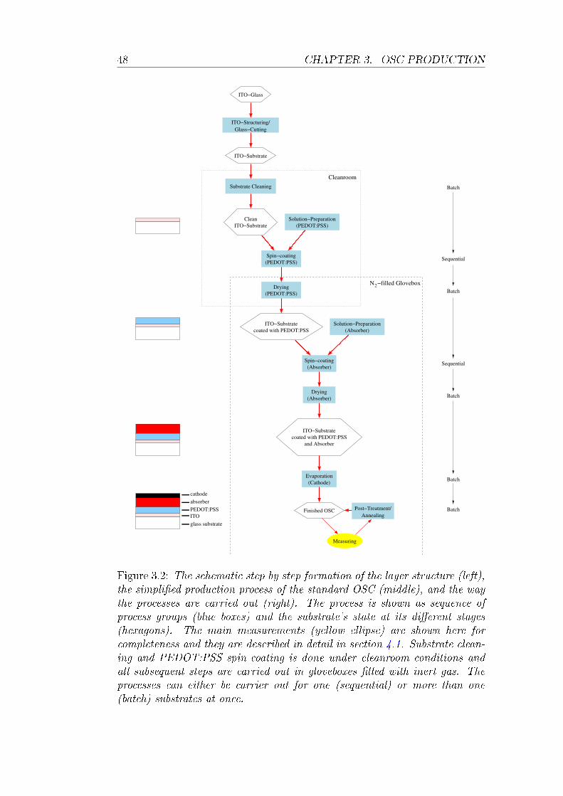
48 CHAPTER 3. OSC PRODUCTION
2N −filled Glovebox
Cleanroom
absorber
PEDOT:PSS
ITO
glass substrate
Sequential
Batch
Batch
Batch
Sequential
Batch
Batch
cathode
Finished OSC
Measuring
ITO−Structuring/
Glass−Cutting
ITO−Glass
ITO−Substrate
Clean
ITO−Substrate
Spin−coating
(PEDOT:PSS)
ITO−Substrate
coated with PEDOT:PSS
Spin−coating
(Absorber)
ITO−Substrate
coated with PEDOT:PSS
and Absorber
(Cathode)
(PEDOT:PSS)
Drying
(PEDOT:PSS)
Solution−Preparation
(Absorber)
Drying
(Absorber)
Evaporation
Post−Treatment/
Annealing
Solution−Preparation
Substrate Cleaning
Figure 3.2: The schematic step by step formation of the layer structure (left),the simplied production process of the standard OSC (middle), and the waythe processes are carried out (right). The process is shown as sequence ofprocess groups (blue boxes) and the substrate's state at its dierent stages(hexagons). The main measurements (yellow ellipse) are shown here forcompleteness and they are described in detail in section 4.1. Substrate clean-ing and PEDOT:PSS spin-coating is done under cleanroom conditions andall subsequent steps are carried out in gloveboxes lled with inert gas. Theprocesses can either be carrier out for one (sequential) or more than one(batch) substrates at once.
3.2. OSC PRODUCTION PROCESS 49
plates are cut to so-called ITO-substrates of 25×25mm2 and subsequently
each substrate is engraved with an unique identier (ID). This ID is used to
continuously track the substrates during production and characterisation.
The cut and engraved substrates are then thoroughly cleaned, starting by
manually wiping them using glass detergent in order to remove dust from
structuring, cutting and storing. This treatment is followed by two acetone
and two isopropanol treatments and a nal bath in deionised (DI) water (all
600s), all with sonication. If necessary the substrates are stored in a separate
beaker lled with DI water until the production continues after cleaning. The
wet cleaning is usually carried out in batches of 24 substrates. When needed,
the substrates are taken out of the DI water and immediately blow dried
with nitrogen. Subsequently their ITO-side is exposed to ozone in a UV-
photoreactor (1200s) to remove any organic residue. Additionally it has been
shown that the UV-ozone treatment modies the surface's wetting properties,
reduces the surface roughness and increases the work function of ITO [57].
The clean ITO-substrate is then ready for the next process step. Clean
substrates, or in general, clean surfaces, are essential for OSCs, because the
layers of an OSC are much thinner (< 300nm) than an average dust particle
(several µm diameter). Any contamination would have a negative eect on
the OSC by introducing unwanted inhomogeneities in the thin layers. Hence
the last two cleaning steps, i.e. the cleaning in DI-water and the UV-ozone
treatment, are carried out directly before the next process group, in the case
of the standard OSCs the spin-coating with PEDOT:PSS. The parameters
recorded during substrate cleaning are shown in table 3.2.
3.2.2 Solution Preparation
The second main preparation step is the preparation of the solutions to be
used for spin-coating. Two dierent kinds of solutions are the basis for the
organic layers of an OSC: the PEDOT:PSS solution1 for the polymeric an-
ode and a solution, consisting of a mixture of polymer and PCBM, for the
photovoltaic active blend layer.
1Technically, PEDOT:PSS is a colloidal suspension, but the term solution will be usedas in coating solution.
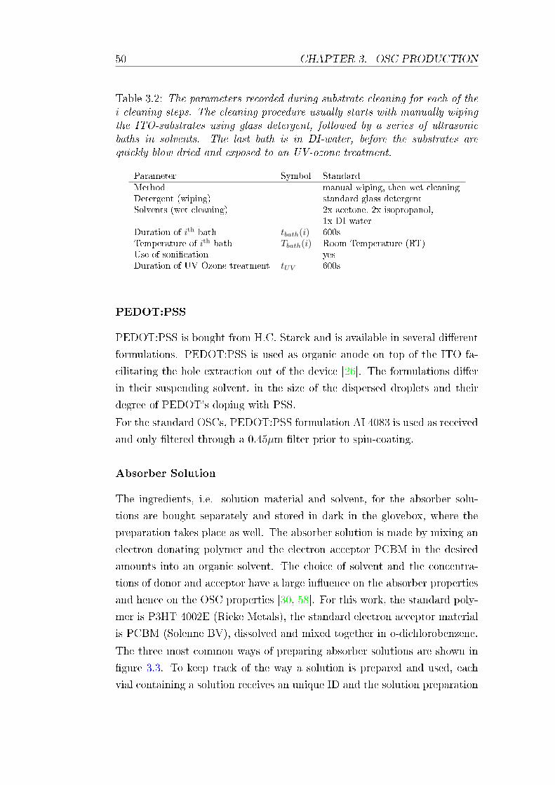
50 CHAPTER 3. OSC PRODUCTION
Table 3.2: The parameters recorded during substrate cleaning for each of thei cleaning steps. The cleaning procedure usually starts with manually wipingthe ITO-substrates using glass detergent, followed by a series of ultrasonicbaths in solvents. The last bath is in DI-water, before the substrates arequickly blow dried and exposed to an UV-ozone treatment.
Parameter Symbol StandardMethod manual wiping, then wet cleaningDetergent (wiping) standard glass detergentSolvents (wet cleaning) 2x acetone, 2x isopropanol,
1x DI waterDuration of ith bath tbath(i) 600sTemperature of ith bath Tbath(i) Room Temperature (RT)Use of sonication yesDuration of UV-Ozone treatment tUV 600s
PEDOT:PSS
PEDOT:PSS is bought from H.C. Starck and is available in several dierent
formulations. PEDOT:PSS is used as organic anode on top of the ITO fa-
cilitating the hole extraction out of the device [26]. The formulations dier
in their suspending solvent, in the size of the dispersed droplets and their
degree of PEDOT's doping with PSS.
For the standard OSCs, PEDOT:PSS formulation AI 4083 is used as received
and only ltered through a 0.45µm lter prior to spin-coating.
Absorber Solution
The ingredients, i.e. solution material and solvent, for the absorber solu-
tions are bought separately and stored in dark in the glovebox, where the
preparation takes place as well. The absorber solution is made by mixing an
electron donating polymer and the electron acceptor PCBM in the desired
amounts into an organic solvent. The choice of solvent and the concentra-
tions of donor and acceptor have a large inuence on the absorber properties
and hence on the OSC properties [30, 58]. For this work, the standard poly-
mer is P3HT 4002E (Rieke Metals), the standard electron acceptor material
is PCBM (Solenne BV), dissolved and mixed together in o-dichlorobenzene.
The three most common ways of preparing absorber solutions are shown in
gure 3.3. To keep track of the way a solution is prepared and used, each
vial containing a solution receives an unique ID and the solution preparation
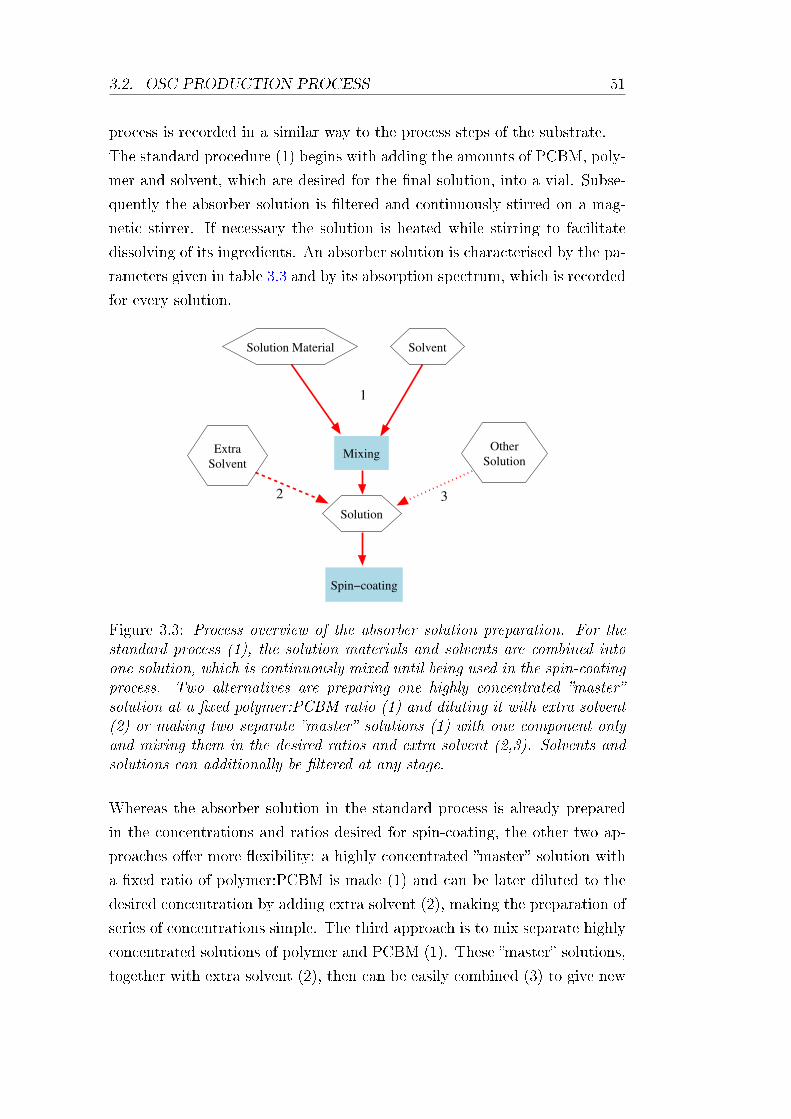
3.2. OSC PRODUCTION PROCESS 51
process is recorded in a similar way to the process steps of the substrate.
The standard procedure (1) begins with adding the amounts of PCBM, poly-
mer and solvent, which are desired for the nal solution, into a vial. Subse-
quently the absorber solution is ltered and continuously stirred on a mag-
netic stirrer. If necessary the solution is heated while stirring to facilitate
dissolving of its ingredients. An absorber solution is characterised by the pa-
rameters given in table 3.3 and by its absorption spectrum, which is recorded
for every solution.
2 3
1
Solution Material
Mixing
Solution
Solvent
Extra
Solvent
Other
Solution
Spin−coating
Figure 3.3: Process overview of the absorber solution preparation. For thestandard process (1), the solution materials and solvents are combined intoone solution, which is continuously mixed until being used in the spin-coatingprocess. Two alternatives are preparing one highly concentrated mastersolution at a xed polymer:PCBM ratio (1) and diluting it with extra solvent(2) or making two separate master solutions (1) with one component onlyand mixing them in the desired ratios and extra solvent (2,3). Solvents andsolutions can additionally be ltered at any stage.
Whereas the absorber solution in the standard process is already prepared
in the concentrations and ratios desired for spin-coating, the other two ap-
proaches oer more exibility: a highly concentrated master solution with
a xed ratio of polymer:PCBM is made (1) and can be later diluted to the
desired concentration by adding extra solvent (2), making the preparation of
series of concentrations simple. The third approach is to mix separate highly
concentrated solutions of polymer and PCBM (1). These master solutions,
together with extra solvent (2), then can be easily combined (3) to give new
52 CHAPTER 3. OSC PRODUCTION
Table 3.3: The parameters characterising an absorber solution. An absorbersolution usually consists of two components: an electron donor and an elec-tron acceptor. The standard materials are P3HT (4002E, Rieke Metals) andPCBM (Solenne BV) respectively.
Parameter Symbol StandardMixing method Magnetic StirrerMixing temperature Tmix ambientElectron donor P3HT (4002E, Rieke Metals)Electron acceptor PCBM (Solenne BV)Concentration of donor cD 10-30mg per mlConcentration of acceptor cA 10-30mg per mlSolvent o-dichlorobenzene (DCB)Solution lter 0.45µm PTFE Membrane
solutions at the desired concentration and ratios. The latter method is the
most exible, yet requires the most preparation steps. These three ways are
not mutually exclusive, but simply oer dierent degrees of exibility.
Filtering the solution after preparation is a necessary step to reduce the impu-
rities contained in the solution, which would otherwise create inhomogeneities
in the absorber lm during spin-coating (see section 3.2.3). However, when
a solution is ltered, a certain amount of the polymer and the PCBM are re-
tained in the lter. Thus the concentration of the solution after ltering will
have changed slightly, making the comparison between absorber solutions,
which were ltered separately, dicult.
3.2.3 Spin-coating and Drying of the organic Layers
Spin-coating is a common method of application of thin lms to substrates.
The concept is shown in gure 3.4 (left). The substrate is held xed on a
vacuum chuck, the solution dispensed on the substrate and the substrate then
spun at high speeds. During spinning a thin wet lm forms on the substrate.
The solvent evaporates both during and after spin-coating [59]. Although
only one substrate can be coated at once, this method is simple and for
laboratory purpose sucient. However, the sequential processing introduces
dierent time intervals the substrates have to wait before and after spin-
coating due to the change from and to a batch process respectively. The
main drawbacks of this method are the high loss of solution (>90%) and
the limitations to substrate size. However, for investigating the physics of
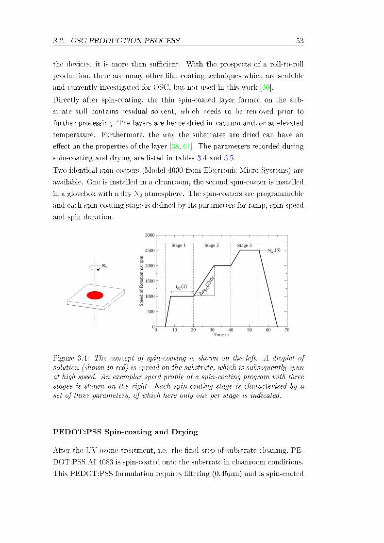
3.2. OSC PRODUCTION PROCESS 53
the devices, it is more than sucient. With the prospects of a roll-to-roll
production, there are many other lm coating techniques which are scalable
and currently investigated for OSC, but not used in this work [60].
Directly after spin-coating, the thin spin-coated layer formed on the sub-
strate still contains residual solvent, which needs to be removed prior to
further processing. The layers are hence dried in vacuum and/or at elevated
temperature. Furthermore, the way the substrates are dried can have an
eect on the properties of the layer [38, 61]. The parameters recorded during
spin-coating and drying are listed in tables 3.4 and 3.5.
Two identical spin-coaters (Model 4000 from Electronic Micro Systems) are
available. One is installed in a cleanroom, the second spin-coater is installed
in a glovebox with a dry N2 atmosphere. The spin-coaters are programmable
and each spin-coating stage is dened by its parameters for ramp, spin speed
and spin duration.
ωsc
0 10 20 30 40 50 60 70Time / s
0
500
1000
1500
2000
2500
3000
Spee
d of
Rot
atio
n ω
/ rp
m
Stage 1 Stage 2 Stage 3
tSC(1)
ωSC(3)
∆ωSC
(2)/∆
t
Figure 3.4: The concept of spin-coating is shown on the left. A droplet ofsolution (shown in red) is spread on the substrate, which is subsequently spunat high speed. An exemplar speed prole of a spin-coating program with threestages is shown on the right. Each spin-coating stage is characterised by aset of three parameters, of which here only one per stage is indicated.
PEDOT:PSS Spin-coating and Drying
After the UV-ozone treatment, i.e. the nal step of substrate cleaning, PE-
DOT:PSS AI 4083 is spin-coated onto the substrate in cleanroom conditions.
This PEDOT:PSS formulation requires ltering (0.45µm) and is spin-coated
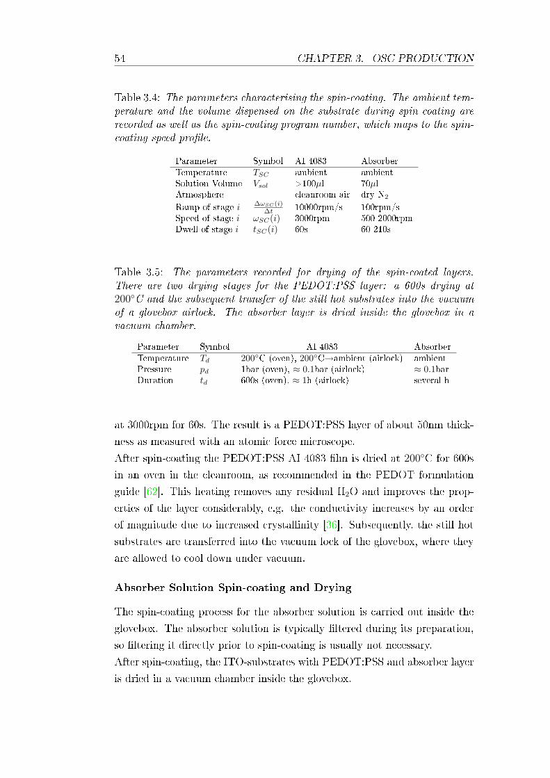
54 CHAPTER 3. OSC PRODUCTION
Table 3.4: The parameters characterising the spin-coating. The ambient tem-perature and the volume dispensed on the substrate during spin-coating arerecorded as well as the spin-coating program number, which maps to the spin-coating speed prole.
Parameter Symbol AI 4083 AbsorberTemperature TSC ambient ambientSolution Volume Vsol >100µl 70µlAtmosphere cleanroom air dry N2
Ramp of stage i ∆ωSC(i)∆t 10000rpm/s 100rpm/s
Speed of stage i ωSC(i) 3000rpm 500-2000rpmDwell of stage i tSC(i) 60s 60-210s
Table 3.5: The parameters recorded for drying of the spin-coated layers.There are two drying stages for the PEDOT:PSS layer: a 600s drying at200C and the subsequent transfer of the still hot substrates into the vacuumof a glovebox airlock. The absorber layer is dried inside the glovebox in avacuum chamber.
Parameter Symbol AI 4083 AbsorberTemperature Td 200C (oven), 200C→ambient (airlock) ambientPressure pd 1bar (oven), ≈ 0.1bar (airlock) ≈ 0.1barDuration td 600s (oven), ≈ 1h (airlock) several h
at 3000rpm for 60s. The result is a PEDOT:PSS layer of about 50nm thick-
ness as measured with an atomic force microscope.
After spin-coating the PEDOT:PSS AI 4083 lm is dried at 200C for 600s
in an oven in the cleanroom, as recommended in the PEDOT formulation
guide [62]. This heating removes any residual H2O and improves the prop-
erties of the layer considerably, e.g. the conductivity increases by an order
of magnitude due to increased crystallinity [36]. Subsequently, the still hot
substrates are transferred into the vacuum lock of the glovebox, where they
are allowed to cool down under vacuum.
Absorber Solution Spin-coating and Drying
The spin-coating process for the absorber solution is carried out inside the
glovebox. The absorber solution is typically ltered during its preparation,
so ltering it directly prior to spin-coating is usually not necessary.
After spin-coating, the ITO-substrates with PEDOT:PSS and absorber layer
is dried in a vacuum chamber inside the glovebox.
3.2. OSC PRODUCTION PROCESS 55
3.2.4 Evaporation of the Cathode
The cathode is realised by evaporating aluminium through a shadow mask
onto the substrates. The active area of the OSC is dened by the overlap of
the shadow mask pattern and the structured ITO electrode.
The evaporation chamber (BOC-Edwards) is equipped with two tungsten
boats for thermal evaporation and one device for electron beam evaporation,
permitting the evaporation of a large variety of metals and dielectrica. De-
pending on the shadow mask, up to nine substrates can be loaded at once into
the evaporation chamber. The chamber is then evacuated. The shadow mask
is attached to a motor inside the evaporation chamber, enabling a continuous
rotation of the mask during evaporation for a homogeneous layer. When a
sucient vacuum is reached (< 5·10−6mbar), the evaporation is started. The
current through the tungsten boats or from the lament of the e-beam source
is manually controlled during the evaporation process. This leads to varia-
tions between dierent batches and repeating exactly the same evaporation
conditions is not possible. The layer thickness is monitored by an oscillating
crystal. The standard cathode consists of about 100nm aluminium, which is
thermally evaporated. The parameters are shown in table 3.6.
The thin lithiumuoride (LiF) layer between absorber and Al-cathode, which
is often seen in literature, is omitted, because it has been reported that the
LiF-Al interface degrades at the temperatures (>140C) the substrates are
exposed to during post-treatment [14].
3.2.5 OSC Post-Treatment/Annealing
For OSCs made from P3HT:PCBM based absorber solutions, a post-treat-
ment (PT, also called annealing) of the OSC after evaporation is a critical
step for its performance. Especially for solutions with fast evaporating sol-
vents, e.g. chlorobenzene, exposing the OSC to a thermal treatment and/or a
prolonged voltage bias can, within certain limits, improve the OSC eciency
considerably. Two major eects are observed. First, small defects in the
absorber layer, which cause shunts and worsen the diode characteristics, are
literally burned out during PT. Second, the short circuit current density Jsc
can substantially be increased due to a combination of increased absorption,
a better mobility of the charge carriers and an improvement of the contacts.
The open circuit voltage Voc and the ll factor FF benet as well, but usually
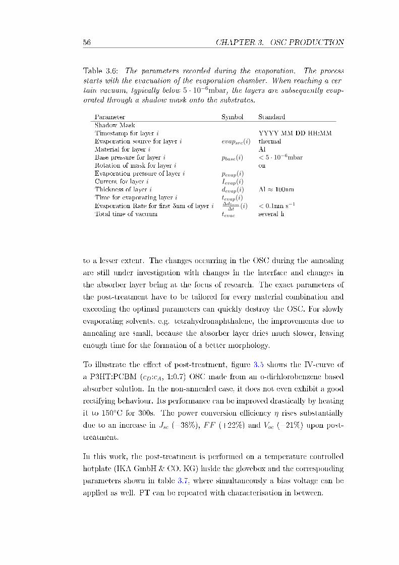
56 CHAPTER 3. OSC PRODUCTION
Table 3.6: The parameters recorded during the evaporation. The processstarts with the evacuation of the evaporation chamber. When reaching a cer-tain vacuum, typically below 5 · 10−6mbar, the layers are subsequently evap-orated through a shadow mask onto the substrates.
Parameter Symbol StandardShadow MaskTimestamp for layer i YYYY-MM-DD HH:MMEvaporation source for layer i evapsrc(i) thermalMaterial for layer i AlBase pressure for layer i pbase(i) < 5 · 10−6mbarRotation of mask for layer i onEvaporation pressure of layer i pevap(i)Current for layer i Ievap(i)Thickness of layer i devap(i) Al ≈ 100nmTime for evaporating layer i tevap(i)Evaporation Rate for rst 5nm of layer i ∆d5nm
∆t (i) < 0.1nm s−1
Total time of vacuum tevac several h
to a lesser extent. The changes occurring in the OSC during the annealing
are still under investigation with changes in the interface and changes in
the absorber layer being at the focus of research. The exact parameters of
the post-treatment have to be tailored for every material combination and
exceeding the optimal parameters can quickly destroy the OSC. For slowly
evaporating solvents, e.g. tetrahydronaphthalene, the improvements due to
annealing are small, because the absorber layer dries much slower, leaving
enough time for the formation of a better morphology.
To illustrate the eect of post-treatment, gure 3.5 shows the IV-curve of
a P3HT:PCBM (cD:cA, 1:0.7) OSC made from an o-dichlorobenzene based
absorber solution. In the non-annealed case, it does not even exhibit a good
rectifying behaviour. Its performance can be improved drastically by heating
it to 150C for 300s. The power conversion eciency η rises substantially
due to an increase in Jsc (+38%), FF (+22%) and Voc (+21%) upon post-
treatment.
In this work, the post-treatment is performed on a temperature controlled
hotplate (IKA GmbH & CO. KG) inside the glovebox and the corresponding
parameters shown in table 3.7, where simultaneously a bias voltage can be
applied as well. PT can be repeated with characterisation in between.
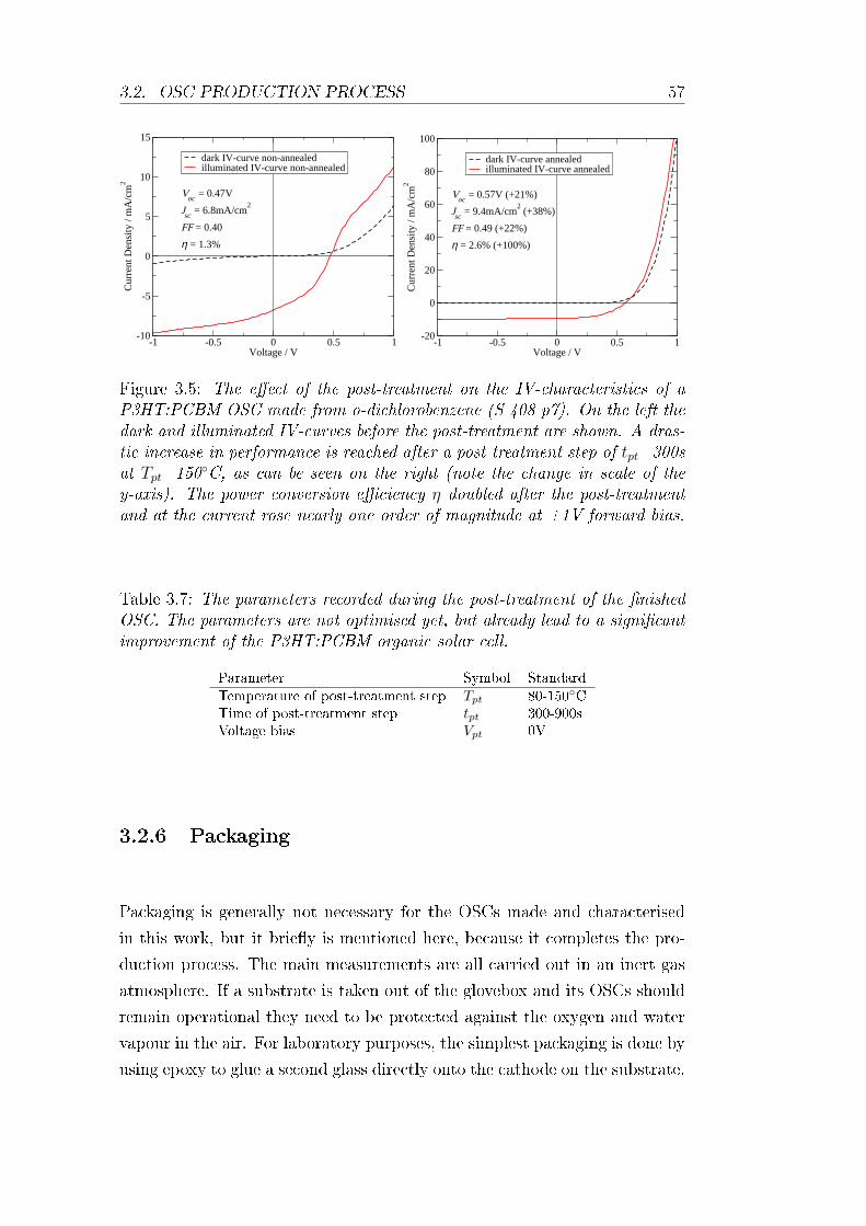
3.2. OSC PRODUCTION PROCESS 57
-1 -0.5 0 0.5 1Voltage / V
-10
-5
0
5
10
15C
urre
nt D
ensi
ty /
mA
/cm
2
dark IV-curve non-annealedilluminated IV-curve non-annealed
Voc = 0.47V
Jsc = 6.8mA/cm2
FF = 0.40
η = 1.3%
Tue Nov 28 13:13:59 2006
-1 -0.5 0 0.5 1Voltage / V
-20
0
20
40
60
80
100
Cur
rent
Den
sity
/ m
A/c
m2
dark IV-curve annealedilluminated IV-curve annealed
Voc = 0.57V (+21%)
FF = 0.49 (+22%)
η = 2.6% (+100%)
Jsc = 9.4mA/cm2 (+38%)
Tue Nov 28 13:13:25 2006
Figure 3.5: The eect of the post-treatment on the IV-characteristics of aP3HT:PCBM OSC made from o-dichlorobenzene (S 408 p7). On the left thedark and illuminated IV-curves before the post-treatment are shown. A dras-tic increase in performance is reached after a post-treatment step of tpt=300sat Tpt=150
C, as can be seen on the right (note the change in scale of they-axis). The power conversion eciency η doubled after the post-treatmentand at the current rose nearly one order of magnitude at +1V forward bias.
Table 3.7: The parameters recorded during the post-treatment of the nishedOSC. The parameters are not optimised yet, but already lead to a signicantimprovement of the P3HT:PCBM organic solar cell.
Parameter Symbol StandardTemperature of post-treatment step Tpt 80-150CTime of post-treatment step tpt 300-900sVoltage bias Vpt 0V
3.2.6 Packaging
Packaging is generally not necessary for the OSCs made and characterised
in this work, but it briey is mentioned here, because it completes the pro-
duction process. The main measurements are all carried out in an inert gas
atmosphere. If a substrate is taken out of the glovebox and its OSCs should
remain operational they need to be protected against the oxygen and water
vapour in the air. For laboratory purposes, the simplest packaging is done by
using epoxy to glue a second glass directly onto the cathode on the substrate.
58 CHAPTER 3. OSC PRODUCTION
3.3 Summary
• The OSC production process was structured and analysed for the pa-
rameters necessary to describe a standardised production process on
a laboratory scale. Despite the simple production, more than 40 pro-
duction parameters were found, which are now routinely recorded for
every substrate.
• The production process consists of a sequence of process steps, of which
most can be carried out for several substrates at once, e.g. the sub-
strate cleaning, and a few only for one substrate at a time, e.g. the
PEDOT:PSS spin-coating. One batch typically consists of eight sub-
strates.
• Most of the production parameters can be controlled very well, e.g. the
spin-coating speed for the PEDOT:PSS or the absorber layer. These
parameters can be made identical for any desired number of substrates.
• The time intervals before and after spin-coating dier always for the
substrates within one batch due the sequential nature of the process.
However, they had not been considered at all before during the analysis
of the measured data.
• A few parameters cannot be fully controlled with the present equip-
ment. E.g. two evaporation processes cannot be made identical due to
the manual control of the evaporation process.
Chapter 4
Measurement Methods and
Automation
In this chapter the measurement methods and their automation are de-
scribed. The measurement concepts and their basic setups are shown and
sources of measurement errors are discussed in the rst part of this chap-
ter. The second part focuses on the automation of these methods, which is
paramount for a reliable and fast characterisation of the organic solar cells
(OSCs).
4.1 Measurement Methods
Three main measurement methods for OSCs are presented in this section.
They are current-voltage measurements, spectral response measurements and
absorption measurements, all of which are performed inside gloveboxes in
a nitrogen atmosphere. These methods are supplemented by atomic force
microscopy (AFM) and impedance measurements.
4.1.1 Current-Voltage Measurement
The current-voltage measurement, short IV-measurement, is the standard
measurement for characterising solar cells. A linear voltage sweep, in our
case usually between ±1V, is applied to the OSC and the resulting current
I in the circuit is measured. In order to allow comparison between dierent
solar cells the current is usually scaled to J , the current density being an
intensive property. The measurement is carried out both without and with
illumination. In the dark, the IV-curve shows a diodic behaviour; under
illumination, extra charge carriers are generated in the solar cell and the
59
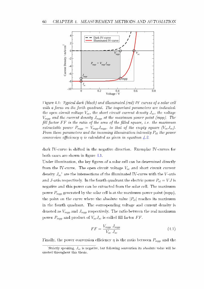
60 CHAPTER 4. MEASUREMENT METHODS AND AUTOMATION
0 0.2 0.4 0.6 0.8Voltage / V
-10
-8
-6
-4
-2
0
2
4
Cur
rent
Den
sity
/ m
A/c
m2
Dark IV-curveIlluminated IV-curve
Voc
Jsc
Vmpp
Jmpp
Pmpp = VmppJmpp
mpp
Figure 4.1: Typical dark (black) and illuminated (red) IV-curves of a solar cellwith a focus on the forth quadrant. The important parameters are indicated:the open circuit voltage Voc, the short circuit current density Jsc, the voltageVmpp and the current density Jmpp at the maximum power point (mpp). Thell factor FF is the ratio of the area of the lled square, i.e. the maximumextractable power Pmpp = VmppJmpp, to that of the empty square (VocJsc).From these parameters and the incoming illumination intensity Pill the powerconversion eciency η is calculated as given in equation 4.2.
dark IV-curve is shifted in the negative direction. Exemplar IV-curves for
both cases are shown in gure 4.1.
Under illumination, the key gures of a solar cell can be determined directly
from the IV-curve. The open circuit voltage Voc and short circuit current
density Jsc1 are the intersections of the illuminated IV-curve with the V -axis
and J-axis respectively. In the fourth quadrant the electric power Pel = V J is
negative and this power can be extracted from the solar cell. The maximum
power Pmpp generated by the solar cell is at the maximum power point (mpp),
the point on the curve where the absolute value |Pel| reaches its maximumin the fourth quadrant. The corresponding voltage and current density is
denoted as Vmpp and Jmpp respectively. The ratio between the real maximum
power Pmpp and product of VocJsc is called ll factor FF .
FF =Vmpp Jmpp
Voc Jsc
(4.1)
Finally, the power conversion eciency η is the ratio between Pmpp and the
1Strictly speaking, Jsc is negative, but following convention its absolute value will bequoted throughout this thesis.
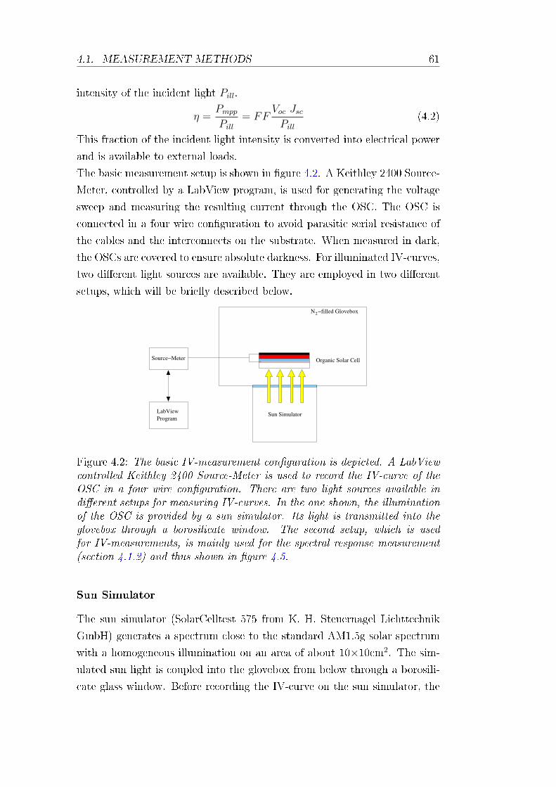
4.1. MEASUREMENT METHODS 61
intensity of the incident light Pill.
η =Pmpp
Pill
= FFVoc Jsc
Pill
(4.2)
This fraction of the incident light intensity is converted into electrical power
and is available to external loads.
The basic measurement setup is shown in gure 4.2. A Keithley 2400 Source-
Meter, controlled by a LabView program, is used for generating the voltage
sweep and measuring the resulting current through the OSC. The OSC is
connected in a four wire conguration to avoid parasitic serial resistance of
the cables and the interconnects on the substrate. When measured in dark,
the OSCs are covered to ensure absolute darkness. For illuminated IV-curves,
two dierent light sources are available. They are employed in two dierent
setups, which will be briey described below.
LabViewProgram
Source−Meter
N −filled Glovebox2
Sun Simulator
Organic Solar Cell
Figure 4.2: The basic IV-measurement conguration is depicted. A LabViewcontrolled Keithley 2400 Source-Meter is used to record the IV-curve of theOSC in a four wire conguration. There are two light sources available indierent setups for measuring IV-curves. In the one shown, the illuminationof the OSC is provided by a sun simulator. Its light is transmitted into theglovebox through a borosilicate window. The second setup, which is usedfor IV-measurements, is mainly used for the spectral response measurement(section 4.1.2) and thus shown in gure 4.5.
Sun Simulator
The sun simulator (SolarCelltest 575 from K. H. Steuernagel Lichttechnik
GmbH) generates a spectrum close to the standard AM1.5g solar spectrum
with a homogeneous illumination on an area of about 10×10cm2. The sim-
ulated sun light is coupled into the glovebox from below through a borosili-
cate glass window. Before recording the IV-curve on the sun simulator, the
62 CHAPTER 4. MEASUREMENT METHODS AND AUTOMATION
illumination intensity is measured with a calibrated solar cell (LOTSDSC5,
Fraunhofer ISE Callab) and corrected for the spectral mismatch (see sec-
tion 4.1.2) such that the OSC generates the Jsc which it would have when
exposed to an intensity of 1000W/m2 with the spectrum of the sun. While
on the sun simulator, all OSCs are cooled by a fan. The temperature for the
OSCs has been measured with a thermocouple and stabilised below 35 C
after ve minutes. IV-measurements were then started after the substrate
temperatures had equilibrated. Although this is not according to the stan-
dard reporting conditions (SRC2), it allows reliable and comparable testing.
Xenon Lamp
In the second setup the illumination is provided by a 1000W Xenon-lamp
with a stabilised power supply (both by company Müller GmbH). This setup
has a dual use. It can be used for IV-curves at dierent illumination in-
tensities and the spectral response, which will be described in section 4.1.2,
can be measured there. The light of the Xe-lamp is coupled into the glove-
box through an optical quartz glass bre cable (custom made by Schölly
Fiberoptic GmbH), with a high transmission into the UV range. The light
beam is homogenised before being focused onto one OSC at a time. The
area of the light spot is approximately 1×1cm2, which is still larger than the
used photovoltaic active area. Variations in the illumination intensity are
achieved by inserting neutral density lters into the light beam in front of
the measured solar cell, allowing intensities between about 2 and 0.001 suns.
Lower intensities are in principle possible, but then the setup requires a bet-
ter shielding against stray light. The lamp intensity is measured in parallel
with a monitor diode to compensate for any lamp drift. The intensity at
the OSC is then calculated using the transmission of the lter and both the
intensity and spectrum of the lamp. This setup is described in more detail in
the section on spectral response measurements (see gure 4.5), because most
components are only necessary there. For IV-measurements all components
of the setup are set such that the white light of the Xe-lamp is transmitted
directly and not being modulated.
2The standard reporting conditions state an illumination of 1000W/m2 with the stan-dard spectrum AM1.5g and the solar cell at 25C.
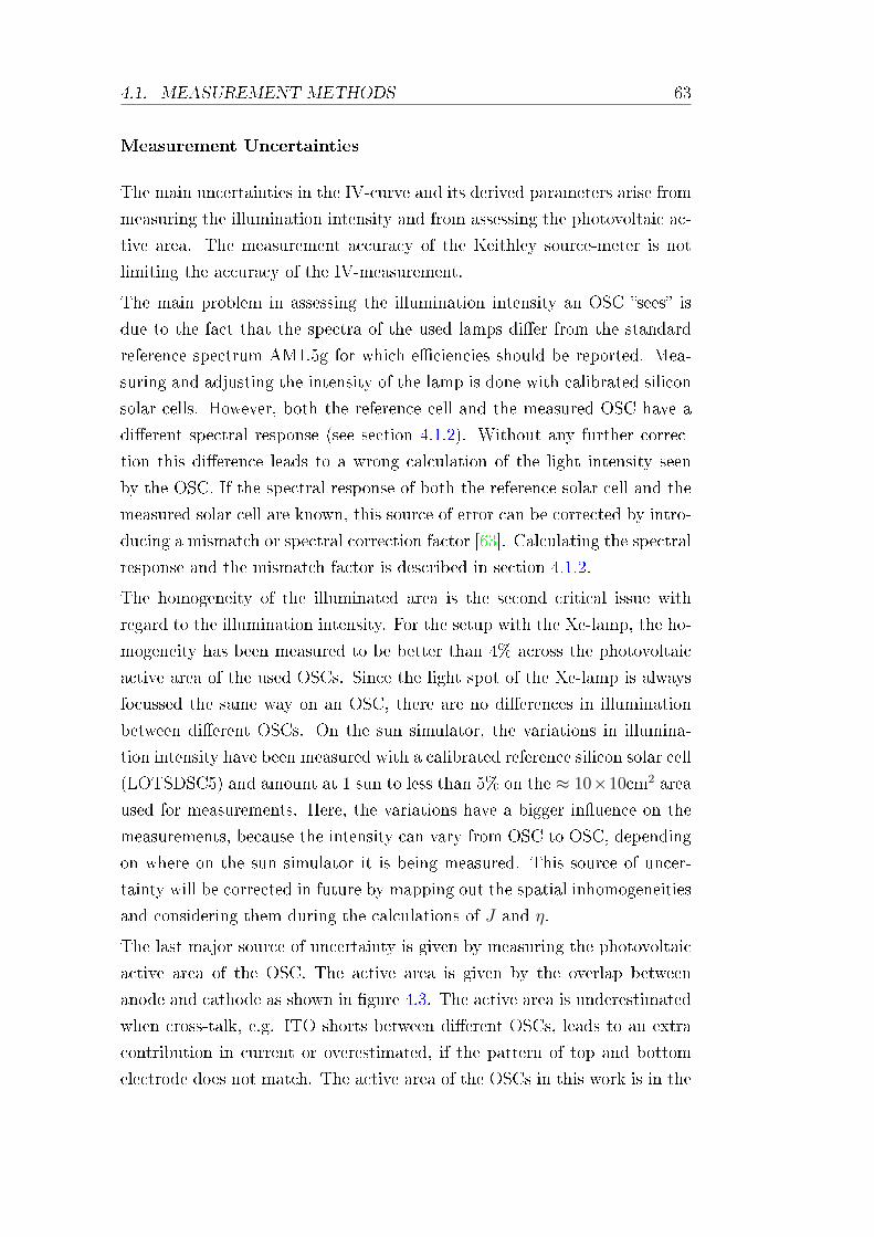
4.1. MEASUREMENT METHODS 63
Measurement Uncertainties
The main uncertainties in the IV-curve and its derived parameters arise from
measuring the illumination intensity and from assessing the photovoltaic ac-
tive area. The measurement accuracy of the Keithley source-meter is not
limiting the accuracy of the IV-measurement.
The main problem in assessing the illumination intensity an OSC sees is
due to the fact that the spectra of the used lamps dier from the standard
reference spectrum AM1.5g for which eciencies should be reported. Mea-
suring and adjusting the intensity of the lamp is done with calibrated silicon
solar cells. However, both the reference cell and the measured OSC have a
dierent spectral response (see section 4.1.2). Without any further correc-
tion this dierence leads to a wrong calculation of the light intensity seen
by the OSC. If the spectral response of both the reference solar cell and the
measured solar cell are known, this source of error can be corrected by intro-
ducing a mismatch or spectral correction factor [63]. Calculating the spectral
response and the mismatch factor is described in section 4.1.2.
The homogeneity of the illuminated area is the second critical issue with
regard to the illumination intensity. For the setup with the Xe-lamp, the ho-
mogeneity has been measured to be better than 4% across the photovoltaic
active area of the used OSCs. Since the light spot of the Xe-lamp is always
focussed the same way on an OSC, there are no dierences in illumination
between dierent OSCs. On the sun simulator, the variations in illumina-
tion intensity have been measured with a calibrated reference silicon solar cell
(LOTSDSC5) and amount at 1 sun to less than 5% on the ≈ 10×10cm2 area
used for measurements. Here, the variations have a bigger inuence on the
measurements, because the intensity can vary from OSC to OSC, depending
on where on the sun simulator it is being measured. This source of uncer-
tainty will be corrected in future by mapping out the spatial inhomogeneities
and considering them during the calculations of J and η.
The last major source of uncertainty is given by measuring the photovoltaic
active area of the OSC. The active area is given by the overlap between
anode and cathode as shown in gure 4.3. The active area is underestimated
when cross-talk, e.g. ITO shorts between dierent OSCs, leads to an extra
contribution in current or overestimated, if the pattern of top and bottom
electrode does not match. The active area of the OSCs in this work is in the
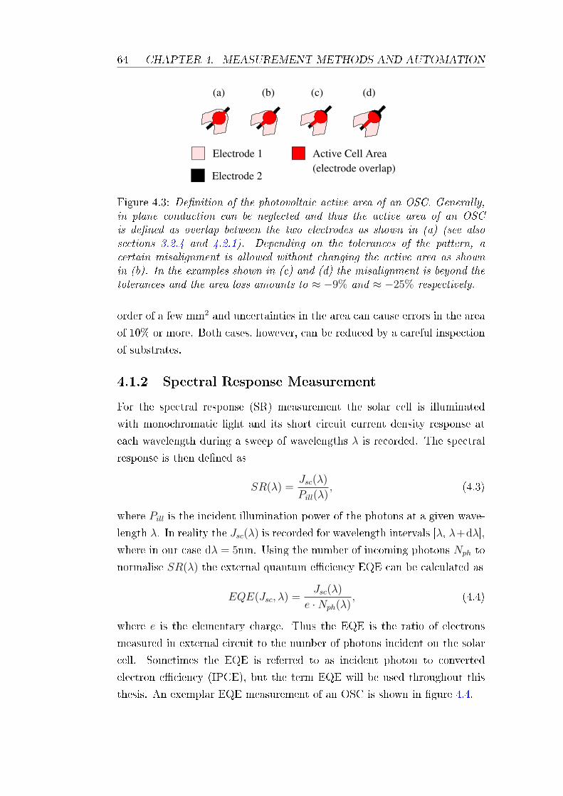
64 CHAPTER 4. MEASUREMENT METHODS AND AUTOMATION
(c)(a) (b) (d)
Electrode 1
Electrode 2
Active Cell Area(electrode overlap)
Figure 4.3: Denition of the photovoltaic active area of an OSC. Generally,in plane conduction can be neglected and thus the active area of an OSCis dened as overlap between the two electrodes as shown in (a) (see alsosections 3.2.4 and 4.2.1). Depending on the tolerances of the pattern, acertain misalignment is allowed without changing the active area as shownin (b). In the examples shown in (c) and (d) the misalignment is beyond thetolerances and the area loss amounts to ≈ −9% and ≈ −25% respectively.
order of a few mm2 and uncertainties in the area can cause errors in the area
of 10% or more. Both cases, however, can be reduced by a careful inspection
of substrates.
4.1.2 Spectral Response Measurement
For the spectral response (SR) measurement the solar cell is illuminated
with monochromatic light and its short circuit current density response at
each wavelength during a sweep of wavelengths λ is recorded. The spectral
response is then dened as
SR(λ) =Jsc(λ)
Pill(λ), (4.3)
where Pill is the incident illumination power of the photons at a given wave-
length λ. In reality the Jsc(λ) is recorded for wavelength intervals [λ, λ+dλ],
where in our case dλ = 5nm. Using the number of incoming photons Nph to
normalise SR(λ) the external quantum eciency EQE can be calculated as
EQE(Jsc, λ) =Jsc(λ)
e ·Nph(λ), (4.4)
where e is the elementary charge. Thus the EQE is the ratio of electrons
measured in external circuit to the number of photons incident on the solar
cell. Sometimes the EQE is referred to as incident photon to converted
electron eciency (IPCE), but the term EQE will be used throughout this
thesis. An exemplar EQE measurement of an OSC is shown in gure 4.4.
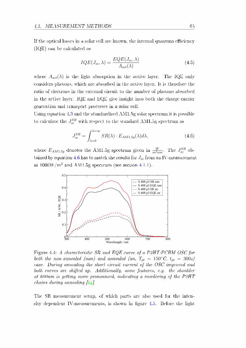
4.1. MEASUREMENT METHODS 65
If the optical losses in a solar cell are known, the internal quantum eciency
(IQE) can be calculated as
IQE(Jsc, λ) =EQE(Jsc, λ)
Aact(λ)(4.5)
where Aact(λ) is the light absorption in the active layer. The IQE only
considers photons, which are absorbed in the active layer. It is therefore the
ratio of electrons in the external circuit to the number of photons absorbed
in the active layer. IQE and EQE give insight into both the charge carrier
generation and transport processes in a solar cell.
Using equation 4.3 and the standardised AM1.5g solar spectrum it is possible
to calculate the JSRsc with respect to the standard AM1.5g spectrum as
JSRsc =
∫ λ=∞
λ=0
SR(λ) · EAM1.5g(λ)dλ, (4.6)
where EAM1.5g denotes the AM1.5g spectrum given in Wm2nm
. The JSRsc ob-
tained by equation 4.6 has to match the results for Jsc from an IV-measurement
at 1000W/m2 and AM1.5g spectrum (see section 4.1.1).
300 400 500 600 700 800Wavelength / nm
0
0.1
0.2
0.3
0.4
0.5
SR /
A/W
, E
QE
S 408 p3 SR nanS 408 p3 EQE nanS 408 p3 SR anS 408 p3 EQE an
Sat Nov 25 10:31:27 2006
Figure 4.4: A characteristic SR and EQE curve of a P3HT:PCBM OSC forboth the non-annealed (nan) and annealed (an, Tpt = 150C, tpt = 300s)case. During annealing the short circuit current of the OSC improved andboth curves are shifted up. Additionally, some features, e.g. the shoulderat 600nm is getting more pronounced, indicating a reordering of the P3HTchains during annealing [64].
The SR measurement setup, of which parts are also used for the inten-
sity dependent IV-measurements, is shown in gure 4.5. Before the light
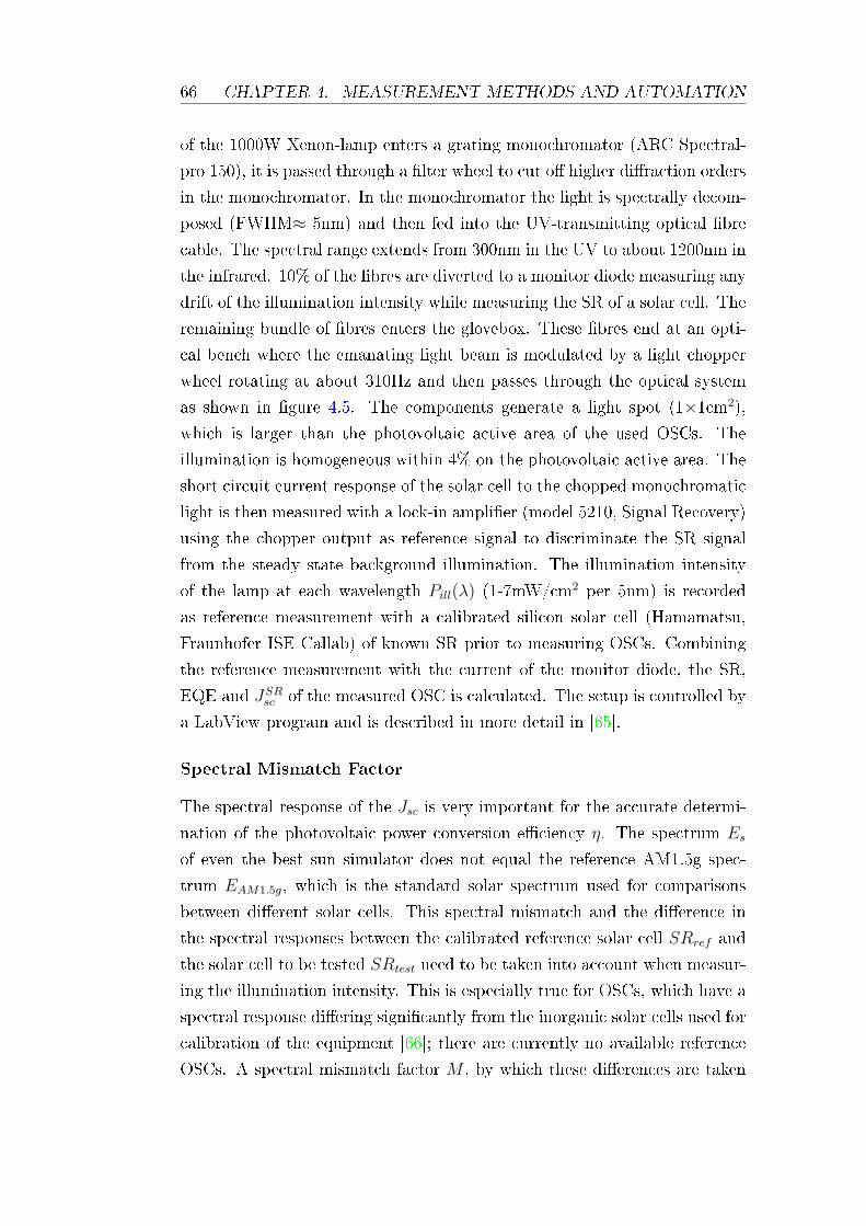
66 CHAPTER 4. MEASUREMENT METHODS AND AUTOMATION
of the 1000W Xenon-lamp enters a grating monochromator (ARC Spectral-
pro 150), it is passed through a lter wheel to cut o higher diraction orders
in the monochromator. In the monochromator the light is spectrally decom-
posed (FWHM≈ 5nm) and then fed into the UV-transmitting optical bre
cable. The spectral range extends from 300nm in the UV to about 1200nm in
the infrared. 10% of the bres are diverted to a monitor diode measuring any
drift of the illumination intensity while measuring the SR of a solar cell. The
remaining bundle of bres enters the glovebox. These bres end at an opti-
cal bench where the emanating light beam is modulated by a light chopper
wheel rotating at about 310Hz and then passes through the optical system
as shown in gure 4.5. The components generate a light spot (1×1cm2),
which is larger than the photovoltaic active area of the used OSCs. The
illumination is homogeneous within 4% on the photovoltaic active area. The
short circuit current response of the solar cell to the chopped monochromatic
light is then measured with a lock-in amplier (model 5210, Signal Recovery)
using the chopper output as reference signal to discriminate the SR signal
from the steady state background illumination. The illumination intensity
of the lamp at each wavelength Pill(λ) (1-7mW/cm2 per 5nm) is recorded
as reference measurement with a calibrated silicon solar cell (Hamamatsu,
Fraunhofer ISE Callab) of known SR prior to measuring OSCs. Combining
the reference measurement with the current of the monitor diode, the SR,
EQE and JSRsc of the measured OSC is calculated. The setup is controlled by
a LabView program and is described in more detail in [65].
Spectral Mismatch Factor
The spectral response of the Jsc is very important for the accurate determi-
nation of the photovoltaic power conversion eciency η. The spectrum Es
of even the best sun simulator does not equal the reference AM1.5g spec-
trum EAM1.5g, which is the standard solar spectrum used for comparisons
between dierent solar cells. This spectral mismatch and the dierence in
the spectral responses between the calibrated reference solar cell SRref and
the solar cell to be tested SRtest need to be taken into account when measur-
ing the illumination intensity. This is especially true for OSCs, which have a
spectral response diering signicantly from the inorganic solar cells used for
calibration of the equipment [66]; there are currently no available reference
OSCs. A spectral mismatch factor M , by which these dierences are taken
4.1. MEASUREMENT METHODS 67
LabViewProgram
2N −filled Glovebox
Filter Wheel
dependent IV−meas.)
(neutral density filter;
only used for int−
Monitor Diode
Chopper Wheel
Iris
Lens
Lens
LensHomogenisor
Signal
Multimeter
Filter Wheel
(Cut−off Filter)
Optical Fibre
Organic Solar Cell
Xe−Lamp
Reference
MonochromatorGrating
Lock−in Amplifier
Figure 4.5: The basic measurement setup for measuring the SR. The light ofa Xe-lamp is spectrally decomposed in a grating monochromator and fed intothe glovebox through an optical bre. The light is modulated by a chopperwheel and passed through a set of optical elements to achieve a homogeneousillumination on the whole solar cell area. A monitor diode measures in par-allel the intensity of the Xe-lamp. The Jsc(λ) is measured via a voltage drop∆V across a resistor by a lock-in amplier receiving the chopper signal asreference. The whole setup is controlled by a LabView program.
into account, is dened as
M =
∫∞0
EAM1.5g(λ)SRref (λ)dλ∫∞
0Es(λ)SRtest(λ)dλ∫∞
0Es(λ)SRref (λ)dλ
∫∞0
EAM1.5g(λ)SRtest(λ)dλ, (4.7)
where Es (in Wm2nm
) has to be known and the SR of reference cell and test cell
can be measured as described above. M is then used to adjust the intensity
of the solar simulator such that the short circuit current Isc of the reference
cell is I0/M , where I0 is its calibration value at SRC. The used reference
cell is a calibrated silicon solar cell (LOTSDSC5), which is equipped with
a colour lter to modify its spectral response such that is closer to SR of
organic solar cells. M is in this case 1.09 on the sun simulator and always
included when stating IV-data.
68 CHAPTER 4. MEASUREMENT METHODS AND AUTOMATION
4.1.3 Absorption Measurement
In the absorption measurement the reection of the light by the OSC is
monitored. For the used OSCs it can be carried out in normal reection
geometry. The highly reective back electrode acts as mirror to the white
incident light shone normal onto the OSC. The reected signal Rsample is then
spectrally decomposed in a spectrometer. In order to calculate the reectivity
R, this spectrum is compared to two reference spectra, which have been
recorded before. The dark reference spectrum Rdark is taken without any
sample (thus no reected signal) to compensate for the background signal
of the bres due to internal reections in the setup. The white reference
spectrum Rwhite is measured with a glass substrate having only a reecting
electrode. The absorption A then can be calculated via the reectivity R as
A = 1−R =Rsample −Rdark
Rwhite −Rdark
. (4.8)
Optical interference eects play an important role for all optical OSC inves-
tigations, because the thickness of the active layer in an OSC is of the same
order of magnitude as the wavelength of the sun or probing light. Small
changes in the layer thickness can have a signicant eect on the absorption
due to interference phenomena. Thus all optical treatment has to be carried
out coherently. In addition to assessing the absorption of an OSC, this mea-
surement is used in conjunction with optical simulations of the layer system
to deduce e.g. estimates for the thickness of the absorber layer.
An Avantes AvaSpec-2048 spectrometer is used in our setup, which is shown
schematically in gure 4.6. It has a CCD with 2048 pixels, leading to a
measurable range of wavelengths from about 280nm to 1000nm (resolution
≈ 0.6nm). The light source consists of two lamps: a deuterium lamp (range
200-400nm) and a halogen lamp (range 400-2000nm). The two lamps and the
spectrometer are each connected to an optical bre cable, which is again led
into the glovebox. Inside the glovebox, the two cables unite in a Y-connection
into one cable, ending in an adjustable lens in front of the measurement sam-
ple. The light, which is coming from the lamps, is reected at the aluminium
interface of the sample and collected by the bre going to the spectrometer.
The spectrometer is controlled by a LabView Program.
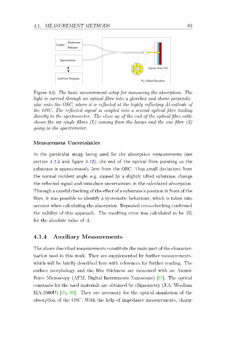
4.1. MEASUREMENT METHODS 69
Deuterium
HalogenLamps:
Spectrometer
LabView ProgramN −filled Glovebox2
Organic Solar Cell
LLL
LL
LS
Figure 4.6: The basic measurement setup for measuring the absorption. Thelight is carried through an optical bre into a glovebox and shone perpendic-ular onto the OSC, where it is reected at the highly reecting Al-cathode ofthe OSC. The reected signal is coupled into a second optical bre leadingdirectly to the spectrometer. The close up of the end of the optical bre cableshows the six single bres (L) coming from the lamps and the one bre (S)going to the spectrometer.
Measurement Uncertainties
In the particular setup being used for the absorption measurements (see
section 4.2.3 and gure 4.12), the end of the optical bre pointing to the
substrate is approximately 5cm from the OSC. Thus small deviations from
the normal incident angle, e.g. caused by a slightly tilted substrate, change
the reected signal and introduce uncertainties in the calculated absorption.
Through a careful checking of the eect of a substrate's position in front of the
bre, it was possible to identify a systematic behaviour, which is taken into
account when calculating the absorption. Repeated cross-checking conrmed
the validity of this approach. The resulting error was calculated to be 5%
for the absolute value of A.
4.1.4 Auxiliary Measurements
The above described measurements constitute the main part of the character-
isation used in this work. They are supplemented by further measurements,
which will be briey described here with references for further reading. The
surface morphology and the lm thickness are measured with an Atomic
Force Microscopy (AFM, Digital Instruments Nanoscope) [67]. The optical
constants for the used materials are obtained by ellipsometry (J.A. Woollam
MA-2000U) [65, 68]. They are necessary for the optical simulation of the
absorption of the OSC. With the help of impedance measurements, charge
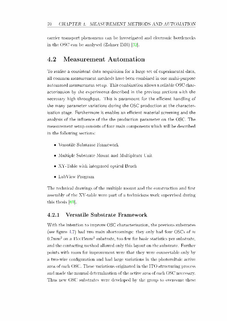
70 CHAPTER 4. MEASUREMENT METHODS AND AUTOMATION
carrier transport phenomena can be investigated and electronic bottlenecks
in the OSC can be analysed (Zahner IM6) [32].
4.2 Measurement Automation
To realise a consistent data acquisition for a large set of experimental data,
all common measurement methods have been combined in one multi-purpose
automated measurement setup. This combination allows a reliable OSC char-
acterisation by the experiments described in the previous sections with the
necessary high throughput. This is paramount for the ecient handling of
the many parameter variations during the OSC production at the character-
isation stage. Furthermore it enables an ecient material screening and the
analysis of the inuence of the the production parameter on the OSC. The
measurement setup consists of four main components which will be described
in the following sections:
• Versatile Substrate Framework
• Multiple Substrate Mount and Multiplexer Unit
• XY-Table with integrated optical Bench
• LabView Program
The technical drawings of the multiple mount and the construction and rst
assembly of the XY-table were part of a technicians work supervised during
this thesis [69].
4.2.1 Versatile Substrate Framework
With the intention to improve OSC characterisation, the previous substrates
(see gure 4.7) had two main shortcomings: they only had four OSCs of ≈0.7mm2 on a 15×15mm2 substrate, too few for basic statistics per substrate,
and the contacting method allowed only this layout on the substrate. Further
points with room for improvement were that they were connectable only by
a two-wire conguration and had large variations in the photovoltaic active
area of each OSC. These variations originated in the ITO structuring process
and made the manual determination of the active area of each OSC necessary.
Thus new OSC substrates were developed by the group to overcome these
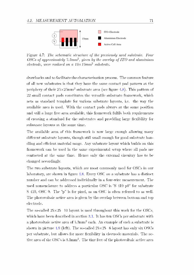
4.2. MEASUREMENT AUTOMATION 71
ITO−Electrode
Aluminium Electrode
Active Cell Area
15mmV
I
Figure 4.7: The schematic structure of the previously used substrate. FourOSCs of approximately 7.5mm2, given by the overlap of ITO and aluminiumelectrode, were realised on a 15×15mm2 substrate.
drawbacks and to facilitate the characterisation process. The common feature
of all new substrates is that they have the same contact pad pattern at the
periphery of their 25×25mm2 substrate area (see gure 4.8). This pattern of
22 small contact pads constitutes the versatile substrate framework, which
acts as standard template for various substrate layouts, i.e. the way the
available area is used. With the contact pads always at the same position
and still a large free area available, this framework fulls both requirements
of creating a standard for the substrates and providing large exibility for
substrate layouts at the same time.
The available area of this framework is now large enough allowing many
dierent substrate layouts, though still small enough for good substrate han-
dling and ecient material usage. Any substrate layout which builds on this
framework can be used in the same experimental setup where all pads are
contacted at the same time. Hence only the external circuitry has to be
changed accordingly.
The two substrate layouts, which are most commonly used for OSCs in our
laboratory, are shown in gure 4.8. Every OSC on a substrate has a distinct
number and can be addressed individually in a four-wire measurement. The
used nomenclature to address a particular OSC is S 419 p9 for substrate
S 419, OSC 9. The p is for pixel, as an OSC is often referred to as well.
The photovoltaic active area is given by the overlap between bottom and top
electrode.
The so-called 25×25_10 layout is used throughout this work for the OSCs,
which have been described in section 3.1. It has ten OSCs per substrate with
a photovoltaic active area of 5.3mm2 each. An example of such a substrate is
shown in picture 4.9 (left). The so-called 25×25_6 layout has only six OSCsper substrate, but allows for more exibility in electrode materials. The ac-
tive area of the OSCs is 8.1mm2. The tiny feet of the photovoltaic active area
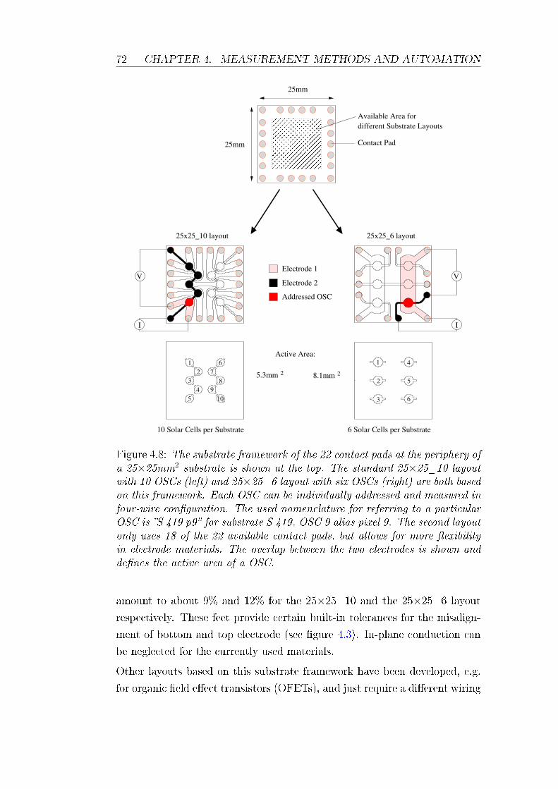
72 CHAPTER 4. MEASUREMENT METHODS AND AUTOMATION
25.3mm 28.1mm
Electrode 2
Electrode 1
Addressed OSC
25mm
Contact Pad
10 Solar Cells per Substrate 6 Solar Cells per Substrate
25mm
25x25_10 layout
Active Area:1
23
45
67
89
10
1
3
4
6
2 5
25x25_6 layout
Available Area fordifferent Substrate Layouts
I
V
I
V
Figure 4.8: The substrate framework of the 22 contact pads at the periphery ofa 25×25mm2 substrate is shown at the top. The standard 25×25_10 layoutwith 10 OSCs (left) and 25×25_6 layout with six OSCs (right) are both basedon this framework. Each OSC can be individually addressed and measured infour-wire conguration. The used nomenclature for referring to a particularOSC is S 419 p9 for substrate S 419, OSC 9 alias pixel 9. The second layoutonly uses 18 of the 22 available contact pads, but allows for more exibilityin electrode materials. The overlap between the two electrodes is shown anddenes the active area of a OSC.
amount to about 9% and 12% for the 25×25_10 and the 25×25_6 layout
respectively. These feet provide certain built-in tolerances for the misalign-
ment of bottom and top electrode (see gure 4.3). In-plane conduction can
be neglected for the currently used materials.
Other layouts based on this substrate framework have been developed, e.g.
for organic eld eect transistors (OFETs), and just require a dierent wiring
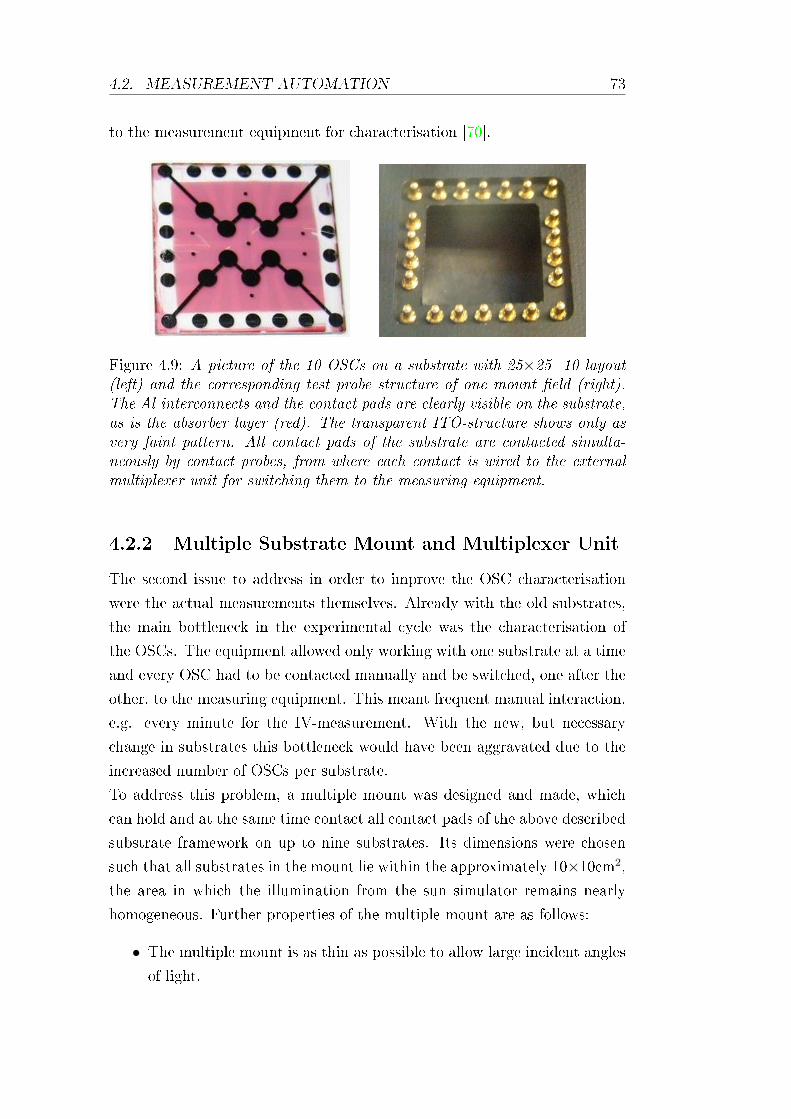
4.2. MEASUREMENT AUTOMATION 73
to the measurement equipment for characterisation [70].
Figure 4.9: A picture of the 10 OSCs on a substrate with 25×25_10 layout(left) and the corresponding test probe structure of one mount eld (right).The Al-interconnects and the contact pads are clearly visible on the substrate,as is the absorber layer (red). The transparent ITO-structure shows only asvery faint pattern. All contact pads of the substrate are contacted simulta-neously by contact probes, from where each contact is wired to the externalmultiplexer unit for switching them to the measuring equipment.
4.2.2 Multiple Substrate Mount and Multiplexer Unit
The second issue to address in order to improve the OSC characterisation
were the actual measurements themselves. Already with the old substrates,
the main bottleneck in the experimental cycle was the characterisation of
the OSCs. The equipment allowed only working with one substrate at a time
and every OSC had to be contacted manually and be switched, one after the
other, to the measuring equipment. This meant frequent manual interaction,
e.g. every minute for the IV-measurement. With the new, but necessary
change in substrates this bottleneck would have been aggravated due to the
increased number of OSCs per substrate.
To address this problem, a multiple mount was designed and made, which
can hold and at the same time contact all contact pads of the above described
substrate framework on up to nine substrates. Its dimensions were chosen
such that all substrates in the mount lie within the approximately 10×10cm2,
the area in which the illumination from the sun simulator remains nearly
homogeneous. Further properties of the multiple mount are as follows:
• The multiple mount is as thin as possible to allow large incident angles
of light.
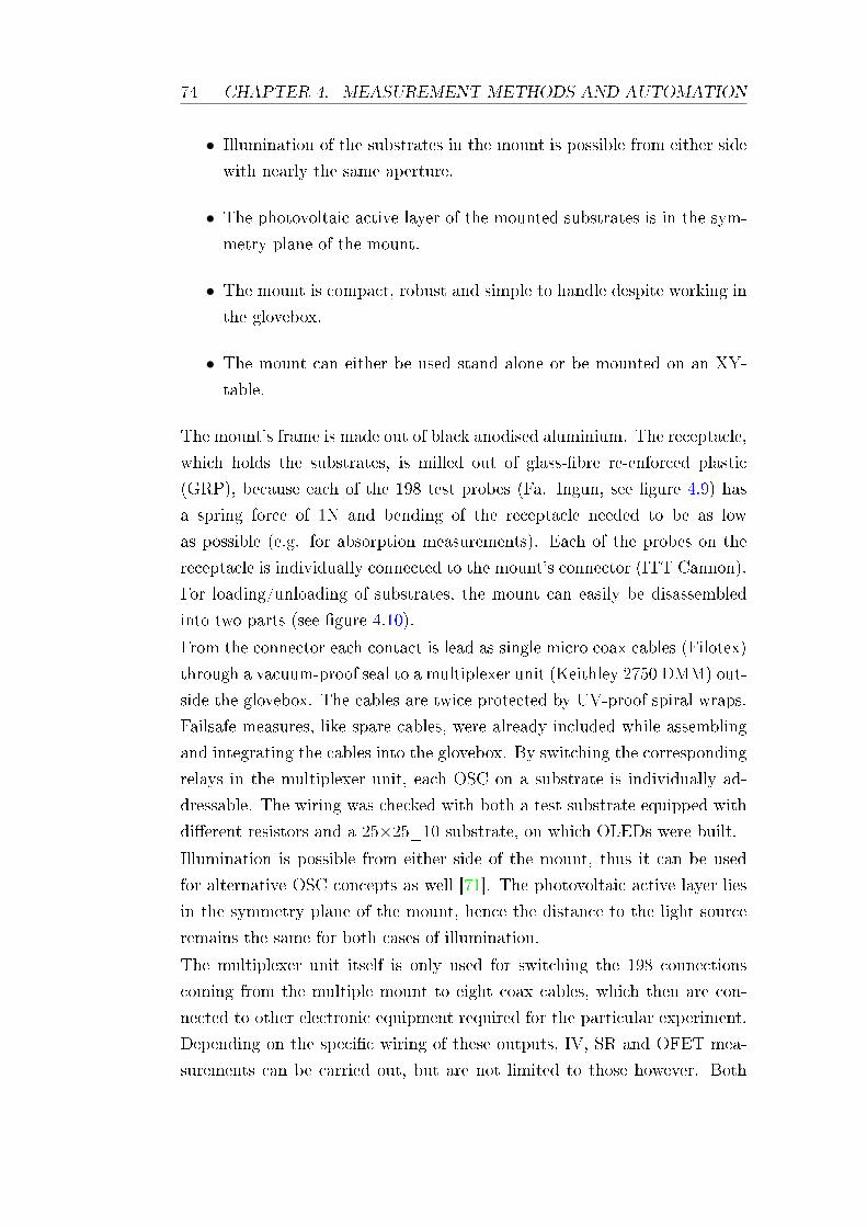
74 CHAPTER 4. MEASUREMENT METHODS AND AUTOMATION
• Illumination of the substrates in the mount is possible from either side
with nearly the same aperture.
• The photovoltaic active layer of the mounted substrates is in the sym-
metry plane of the mount.
• The mount is compact, robust and simple to handle despite working in
the glovebox.
• The mount can either be used stand alone or be mounted on an XY-
table.
The mount's frame is made out of black anodised aluminium. The receptacle,
which holds the substrates, is milled out of glass-bre re-enforced plastic
(GRP), because each of the 198 test probes (Fa. Ingun, see gure 4.9) has
a spring force of 1N and bending of the receptacle needed to be as low
as possible (e.g. for absorption measurements). Each of the probes on the
receptacle is individually connected to the mount's connector (ITT Cannon).
For loading/unloading of substrates, the mount can easily be disassembled
into two parts (see gure 4.10).
From the connector each contact is lead as single micro coax cables (Filotex)
through a vacuum-proof seal to a multiplexer unit (Keithley 2750 DMM) out-
side the glovebox. The cables are twice protected by UV-proof spiral wraps.
Failsafe measures, like spare cables, were already included while assembling
and integrating the cables into the glovebox. By switching the corresponding
relays in the multiplexer unit, each OSC on a substrate is individually ad-
dressable. The wiring was checked with both a test substrate equipped with
dierent resistors and a 25×25_10 substrate, on which OLEDs were built.
Illumination is possible from either side of the mount, thus it can be used
for alternative OSC concepts as well [71]. The photovoltaic active layer lies
in the symmetry plane of the mount, hence the distance to the light source
remains the same for both cases of illumination.
The multiplexer unit itself is only used for switching the 198 connections
coming from the multiple mount to eight coax cables, which then are con-
nected to other electronic equipment required for the particular experiment.
Depending on the specic wiring of these outputs, IV, SR and OFET mea-
surements can be carried out, but are not limited to those however. Both
4.2. MEASUREMENT AUTOMATION 75
switching of the relays and controlling the measurement equipment is done
by the central LabView program.
Finally, the mount is designed such that it can be used standalone for mea-
suring OSCs on the sun simulator, where all mounted substrates can be
illuminated at the same time, or be mounted on its corresponding XY-table,
where OSCs selectively can be illuminated by moving them into the light
beam.
Figure 4.10: The fully loaded mount with nine substrates ready to be measuredis shown on the top. The image at the bottom shows the opened mount whichallows an easy loading/unloading of the substrates onto/from the receptacleon the right.
4.2.3 XY-Table with integrated optical Bench
The versatility of the automated measurement setup is further enhanced by
the option of attaching the multiple mount onto the sled of a computer con-
trolled XY-table. The XY-table had been built such that it easily tted the
76 CHAPTER 4. MEASUREMENT METHODS AND AUTOMATION
existing optical bench, which had already been used for SR measurements.
The sled can move the multiple mount such that each point on the mount
can be positioned accurately in the spot of the light beams coming from the
optical bench and guide pins on the sled ensure that the multiple mount is
always normal to the incident light. The components on the optical bench
are currently congured such that SR, IV-curves (incl. light intensity depen-
dent) and absorption measurements can be carried out on every OSC in the
mount. The sled of the XY-table has a traverse path of about 150×150mm2
and covers enough area such that the setup can be extended by further ex-
periments. The whole construction was kept as compact as possible for the
use inside a glovebox. A picture of the XY-table, optical bench and multiple
mount is shown in gure 4.11. A close-up of the sled is shown in gure 4.12.
The frame of the XY-table is made out of standard aluminium proles and
the sled moves with four double bearing units on rails (all ITEM) for each
x-axis and y-axis. Two stepper motors (Mineba) are connected via Oldham
couplings to miniature ballscrew assemblies (Bosch Rexroth) and drive the
sled. The motors are controlled by the central LabView program addressing
a stepper driver module (310 Trinamic). The double bearing units on the
two rails of the Y-axis are synced by a cam belt. The mount can be xed
on the sled in either the standard or the inverted way such that proper
illumination is provided as desired. Additionally, having not one central
y-axis, but two rails at the frame, leaves the central part of the XY-table
accessible from both sides for further extensions. Great care was devoted
to the positioning accuracy and the repeatability of the sled's moves to less
than 100µm. The table has two high precision reference switches (Euchner),
used to determining the table's reference position before every measurement.
The exact position of the mount in front of the light beam was determined
using a reference diode covered with a mask of small aperture.
4.2.4 LabView Program
The multiple mount, the multiplexer unit, the XY-table and all other mea-
surement components are controlled and tied together by an advanced Lab-
View program. The concept was developed during the course of this thesis
and the programming was carried out by Martin Meier.
The LabView program has a very modular design such that it can easily
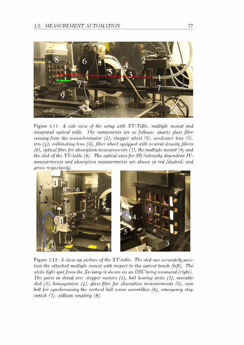
4.2. MEASUREMENT AUTOMATION 77
Figure 4.11: A side view of the setup with XY-Table, multiple mount andintegrated optical table. The components are as follows: quartz glass brecoming from the monochromator (1), chopper wheel (2), condenser lens (3),iris (4), collimating lens (5), lter wheel equipped with neutral density lters(6), optical bre for absorption measurements (7), the multiple mount (8) andthe sled of the XY-table (9). The optical axes for SR/intensity dependent IV-measurements and absorption measurements are shown in red (dashed) andgreen respectively.
Figure 4.12: A close up picture of the XY-table. The sled can accurately posi-tion the attached multiple mount with respect to the optical bench (left). Thewhite light spot from the Xe-lamp is shown on an OSC being measured (right).The parts in detail are: stepper motors (1), ball bearing units (2), movablesled (3), homogeniser (4), glass bre for absorption measurements (5), cambelt for synchronising the vertical ball screw assemblies (6), emergency stopswitch (7), oldham coupling (8).
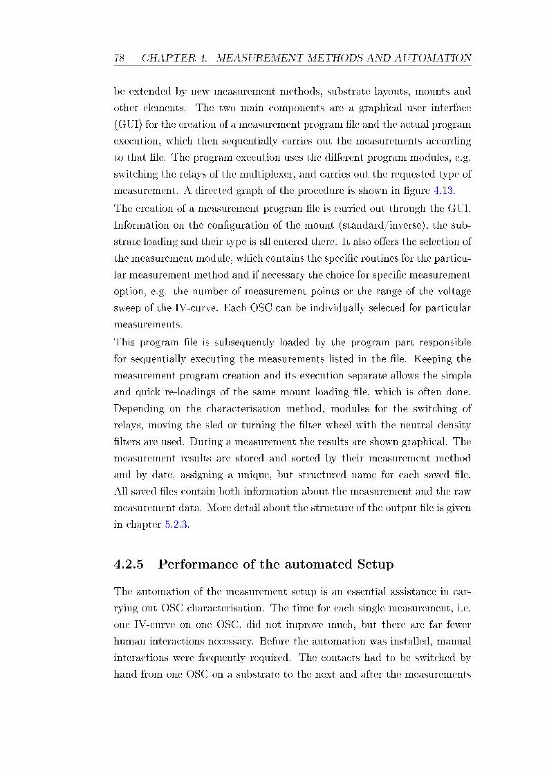
78 CHAPTER 4. MEASUREMENT METHODS AND AUTOMATION
be extended by new measurement methods, substrate layouts, mounts and
other elements. The two main components are a graphical user interface
(GUI) for the creation of a measurement program le and the actual program
execution, which then sequentially carries out the measurements according
to that le. The program execution uses the dierent program modules, e.g.
switching the relays of the multiplexer, and carries out the requested type of
measurement. A directed graph of the procedure is shown in gure 4.13.
The creation of a measurement program le is carried out through the GUI.
Information on the conguration of the mount (standard/inverse), the sub-
strate loading and their type is all entered there. It also oers the selection of
the measurement module, which contains the specic routines for the particu-
lar measurement method and if necessary the choice for specic measurement
option, e.g. the number of measurement points or the range of the voltage
sweep of the IV-curve. Each OSC can be individually selected for particular
measurements.
This program le is subsequently loaded by the program part responsible
for sequentially executing the measurements listed in the le. Keeping the
measurement program creation and its execution separate allows the simple
and quick re-loadings of the same mount loading le, which is often done.
Depending on the characterisation method, modules for the switching of
relays, moving the sled or turning the lter wheel with the neutral density
lters are used. During a measurement the results are shown graphical. The
measurement results are stored and sorted by their measurement method
and by date, assigning a unique, but structured name for each saved le.
All saved les contain both information about the measurement and the raw
measurement data. More detail about the structure of the output le is given
in chapter 5.2.3.
4.2.5 Performance of the automated Setup
The automation of the measurement setup is an essential assistance in car-
rying out OSC characterisation. The time for each single measurement, i.e.
one IV-curve on one OSC, did not improve much, but there are far fewer
human interactions necessary. Before the automation was installed, manual
interactions were frequently required. The contacts had to be switched by
hand from one OSC on a substrate to the next and after the measurements
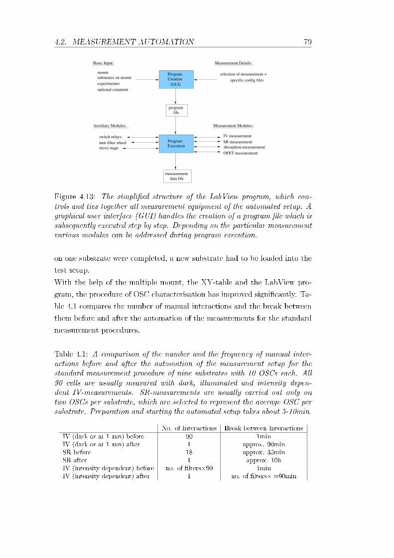
4.2. MEASUREMENT AUTOMATION 79
Auxiliary Modules:
mount
experimentersubstrates on mount
optional comment
switch relaysturn filter wheelmove stage
SR measurementabsorption measurementOFET measurement
IV measurement
Basic Input: Measurement Details:
selection of measurement +specific config files
Measurement Modules:
ProgramExecution
ProgramCreation
(GUI)
measurementdata file
fileprogram
Figure 4.13: The simplied structure of the LabView program, which con-trols and ties together all measurement equipment of the automated setup. Agraphical user interface (GUI) handles the creation of a program le which issubsequently executed step by step. Depending on the particular measurementvarious modules can be addressed during program execution.
on one substrate were completed, a new substrate had to be loaded into the
test setup.
With the help of the multiple mount, the XY-table and the LabView pro-
gram, the procedure of OSC characterisation has improved signicantly. Ta-
ble 4.1 compares the number of manual interactions and the break between
them before and after the automation of the measurements for the standard
measurement procedures.
Table 4.1: A comparison of the number and the frequency of manual inter-actions before and after the automation of the measurement setup for thestandard measurement procedure of nine substrates with 10 OSCs each. All90 cells are usually measured with dark, illuminated and intensity depen-dent IV-measurements. SR-measurements are usually carried out only ontwo OSCs per substrate, which are selected to represent the average OSC persubstrate. Preparation and starting the automated setup takes about 5-10min.
No. of Interactions Break between InteractionsIV (dark or at 1 sun) before 90 1minIV (dark or at 1 sun) after 1 approx. 90minSR before 18 approx. 35minSR after 1 approx. 10hIV (intensity dependent) before no. of lters×90 1minIV (intensity dependent) after 1 no. of lters× ≈90min
80 CHAPTER 4. MEASUREMENT METHODS AND AUTOMATION
For SR-measurements, every 35min the contacts had to be switched manually
to the next OSC and the measurement program had to be restarted, but for
the IV-measurement, the manual interactions were every minute prior to the
automation.
It now takes about 5 to 10 minutes to load the multiple mount and cre-
ate a new measurement program. Once that is done, no further manual
interaction is necessary until the measurement program has nished. For
a fully loaded multiple mount with 10 OSCs per substrate, i.e. 90 OSCs,
the IV-measurement takes about 90min per illumination intensity, whereas
the SR-measurement of two OSCs per substrate takes about 10h. Measur-
ing the SR for every OSC on all nine substrate is possible as well (≈52h),but the extra information gained does not justify the time required during
the standard characterisation cycle. The OSCs for SR measurements are
generally selected such that the represent average OSC on that substrate.
For intensity dependent measurements, each OSC is measured several times
with a dierent neutral density lter, and the length of time for a complete
measurement depends on the numbers of lters used. Typically ve dier-
ent lters are used and for the lowest intensities, the measurement is carried
out twice with dierent ranges of the voltage sweep to get a better resolu-
tion. Hence the measurement runs for about 10h. Both SR and intensity
dependent IV-measurements are well suited for running over night.
Figure 4.14 shows the development in the number of IV and SR measure-
ments along a time line starting with the rst version of the LabView pro-
gram. The dierent components came into use one after the other and the
setup has grown continuously more elaborated. The capabilities of the setup
were extended by the absorption measurement in January 2006, which could
directly be integrated into the automated setup. This proves the simplicity
of extending the capabilities of the measurement setup. Measuring the ab-
sorption of a fully loaded multiple mount with 10 OSCs per substrate takes
about 15min.
The series of exemplar measurements in gure 4.15 shows the range of mea-
surements which can currently be conducted with the automated setup. With
the help of this setup, the characterisation of the OSCs is no bottleneck any-
more.
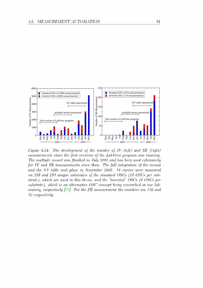
4.2. MEASUREMENT AUTOMATION 81
Mar
Apr
May Jun
Jul
Aug Sep
Oct
Nov
Dec Jan
Feb
Mar
Apr
May
0
1000
2000
3000
4000
5000
6000
Num
ber
of I
V-M
easu
rem
ents
Standard OSCs (12609 measurements)Inverted OSCs (4500 measurements)
2005 2006
multiple mount operational
first version of LabView program
XY-table operational
Sat Nov 25 10:41:30 2006
Mar
Apr
May Jun
Jul
Aug Sep
Oct
Nov
Dec Jan
Feb
Mar
Apr
May
0
50
100
150
200
250
Num
ber
of S
R-M
easu
rem
ents
Standard OSCs (474 measurements)Inverted OSCs (174 measurements)
2005 2006
multiple mount operational
first version of LabView program
XY-table operational
Sat Nov 25 10:41:54 2006
Figure 4.14: The development of the number of IV (left) and SR (right)measurements since the rst versions of the LabView program was running.The multiple mount was nished in July 2005 and has been used extensivelyfor IV and SR measurements since then. The full integration of the mountand the XY-table took place in November 2005. IV-curves were measuredon 259 and 193 unique substrates of the standard OSCs (10 OSCs per sub-strate), which are used in this thesis, and the inverted OSCs (6 OSCs persubstrate), which is an alternative OSC concept being researched in our lab-oratory, respectively [71]. For the SR measurement the numbers are 116 and72 respectively.
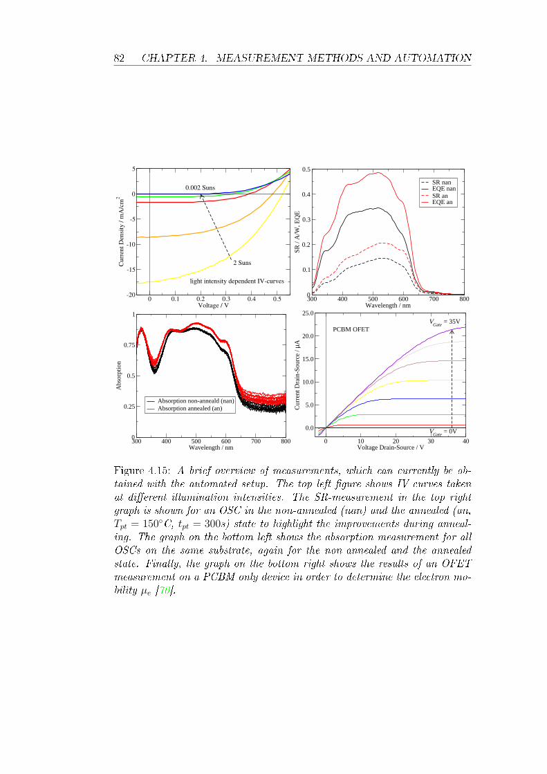
82 CHAPTER 4. MEASUREMENT METHODS AND AUTOMATION
0 0.1 0.2 0.3 0.4 0.5Voltage / V
-20
-15
-10
-5
0
5
Cur
rent
Den
sity
/ m
A/c
m2
2 Suns
0.002 Suns
light intensity dependent IV-curves
Tue Jul 25 23:21:32 2006
300 400 500 600 700 800Wavelength / nm
0
0.1
0.2
0.3
0.4
0.5
SR /
A/W
, EQ
E
SR nanEQE nanSR anEQE an
Sat Nov 25 10:45:50 2006
300 400 500 600 700 800Wavelength / nm
0
0.25
0.5
0.75
1
Abs
orpt
ion
Absorption non-anneald (nan)Absorption annealed (an)
Sat Nov 25 10:44:56 2006
0 10 20 30 40Voltage Drain-Source / V
0.0
5.0
10.0
15.0
20.0
25.0
Cur
rent
Dra
in-S
ourc
e / µ
A
PCBM OFET
VGate = 0V
VGate = 35V
Sat Nov 25 10:47:22 2006
Figure 4.15: A brief overview of measurements, which can currently be ob-tained with the automated setup. The top left gure shows IV-curves takenat dierent illumination intensities. The SR-measurement in the top rightgraph is shown for an OSC in the non-annealed (nan) and the annealed (an,Tpt = 150C, tpt = 300s) state to highlight the improvements during anneal-ing. The graph on the bottom left shows the absorption measurement for allOSCs on the same substrate, again for the non-annealed and the annealedstate. Finally, the graph on the bottom right shows the results of an OFETmeasurement on a PCBM only device in order to determine the electron mo-bility µe [70].
4.3. SUMMARY 83
4.3 Summary
• The standard OSC characterisation methods used are the current-
voltage characteristics (dark/illuminated/intensity dependent), spec-
tral response measurements and absorption measurements.
• To achieve a reliable and ecient characterisation process, the stan-
dard measurements were all integrated into an automated measurement
setup, which consists of a versatile substrate framework, a multiple
mount, an XY-table and a LabView program.
• Due to a versatile and exible substrate framework, dierent substrate
layouts, e.g. substrates with dierent number and types of OSCs or
even with OFETs, have all the same standardised contact structure for
test probes and can be measured in the same experimental setup.
• The multiple mount can hold and contact up to 90 OSCs on nine sub-
strates simultaneously. Via a multiplexer unit, each OSC can individ-
ually be electrically addressed and measured. The multiple mount can
be used directly on the sun simulator or on the XY-table.
• The XY-table can accurately (<0.1mm) position each OSC in the mul-
tiple mount in front of an optical bench, which is equipped with two
optical axes. One axis is used for spectral response measurements and
light intensity dependent current-voltage characteristics, the other for
absorption measurements.
• The central LabView program controls all measurement equipment
which is involved in the automated setup and handles the standard-
ised storage of the measured data.
• The assistance of the automated setup has greatly simplied the char-
acterisation process and freed manpower for other tasks, e.g. the pro-
duction of OSCs.

84 CHAPTER 4. MEASUREMENT METHODS AND AUTOMATION
Chapter 5
Data Analysis Methods and
Environment
In this chapter the methods for the data analysis and the fundamental data
handling and organisation is described. First, the theory of the methods used
for condensing measurement results into useful parameters and for analysing
the data is presented. Then the computational environment, in which the
data analysis is carried out, is specied. At its centre is an electronic lab-
oratory notebook (ELN), which contains all production parameters, mea-
surement data and deduced parameters for every organic solar cell (OSC).
This data then has to be prepared to be of use for the data analysis and the
necessary steps of data preparation are described. The chapter closes with a
brief overview of the computational tools used and the precautions taken to
ensure data and code integrity.
5.1 Data Analysis Methods
The methods used to extract information from measurements and the OSC
preparation process are presented in this chapter. Spline functions are used
for approximating noisy measured data or the Levenberg-Marquardt Algo-
rithm (LMA) for tting models to such data. With the help of the pre-
sented methods, parameters are extracted from the measured data. These
parameters, together with the production parameters, form the data which
is subsequently analysed using the principal component analysis (PCA) in
the search for patterns and trends with physical origin.
85
86 CHAPTER 5. DATA ANALYSIS METHODS AND ENVIRONMENT
5.1.1 Fitting of Functions to Data
Most measurements in this work yield two-dimensional curves, which are
described by a set of data yi taken at discrete points xi (i = 1, . . . , N).
Whereas the values xi of the controlling variable are usually assumed to
be exact, the data yi is generally subject to certain errors, i.e.
yi = f(xi) + εi, (5.1)
where εi is the error in the measurement, which may originate for example
from a normal distribution with standard deviation σi. In order to extract
parameters from the data, e.g. the intersection of the curve with axes or
features like derivatives, often values in between xi and xi+1 or the curve
derivatives at some x are of interest for the analysis. Hence it would be useful
to nd a function f , which adequately approximates the data continuously
while taking the measurement errors into account. Fitting with a polynomial
would be one possibility if there is no prior knowledge about the function to
t. However, using a polynomial, which is globally dened for data with many
data points, might quickly become unfeasible due to the high polynomial
order required for approximation.
A common and ecient method is to describe such data by a function f ,
which is composed of piecewise dened low order polynomials that are smooth-
ly connected. The resulting function is called a spline. Splines are often used
for representing curves, because of their simple construction and easy han-
dling even in more than two dimensions.
Splines are of degree k, if they are composed of polynomials of degree k.
Cubic splines, i.e. k = 3, are the most common type and they are used
in this work to extract OSC properties from measurement data if no model
function is known (see section 5.3.2). Their basics are briey described here
following references [72, 73].
A spline f has to satisfy two main conditions:
1. it has to be as smooth as possible while
2. still approximating the data adequately.
Suppose that set xi is ordered such that x1 < x2 < ... < xN . A measure
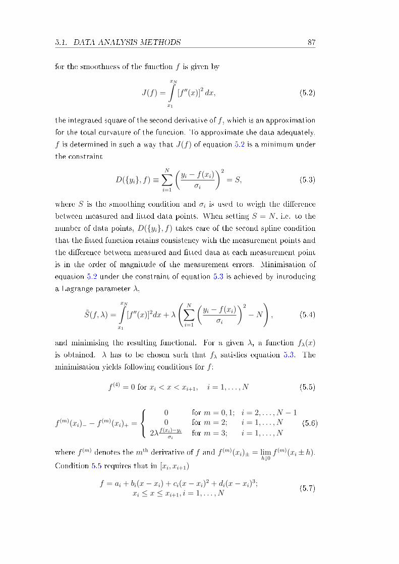
5.1. DATA ANALYSIS METHODS 87
for the smoothness of the function f is given by
J(f) =
xN∫x1
[f ′′(x)]2dx, (5.2)
the integrated square of the second derivative of f , which is an approximation
for the total curvature of the function. To approximate the data adequately,
f is determined in such a way that J(f) of equation 5.2 is a minimum under
the constraint
D(yi, f) ≡N∑
i=1
(yi − f(xi)
σi
)2
= S, (5.3)
where S is the smoothing condition and σi is used to weigh the dierence
between measured and tted data points. When setting S = N , i.e. to the
number of data points, D(yi, f) takes care of the second spline condition
that the tted function retains consistency with the measurement points and
the dierence between measured and tted data at each measurement point
is in the order of magnitude of the measurement errors. Minimisation of
equation 5.2 under the constraint of equation 5.3 is achieved by introducing
a Lagrange parameter λ,
S(f, λ) =
xN∫x1
[f ′′(x)]2dx + λ
(N∑
i=1
(yi − f(xi)
σi
)2
−N
), (5.4)
and minimising the resulting functional. For a given λ, a function fλ(x)
is obtained. λ has to be chosen such that fλ satises equation 5.3. The
minimisation yields following conditions for f :
f (4) = 0 for xi < x < xi+1, i = 1, . . . , N (5.5)
f (m)(xi)− − f (m)(xi)+ =
0 for m = 0, 1; i = 2, . . . , N − 10 for m = 2; i = 1, . . . , N
2λf(xi)−yi
σifor m = 3; i = 1, . . . , N
,(5.6)
where f (m) denotes the mth derivative of f and f (m)(xi)± = limh↓0
f (m)(xi± h).
Condition 5.5 requires that in [xi, xi+1)
f = ai + bi(x− xi) + ci(x− xi)2 + di(x− xi)
3;xi ≤ x ≤ xi+1, i = 1, . . . , N
(5.7)
88 CHAPTER 5. DATA ANALYSIS METHODS AND ENVIRONMENT
with parameters ai, bi, ci, di to be determined. The conditions in equa-
tion 5.6 demand that f is twice continuously dierentiable at all xi, but the
third derivative is discontinuous an amount to be determined. Thus f(x) is
composed of cubic polynomials, which are continuously dierentiable up to
f ′′. The parameters ai, bi, ci, di can be determined from 5.6 and many fast
computational algorithms are available for that purpose.
Splines can be used both for interpolation and smoothing data in two or more
dimensions. The smoothing condition S for curves weighted by σi is usually
chosen in the range of N ±√
2N . Interpolating splines constitute a subset
of the more general smoothing splines. Here S = 0 and the resulting spline
goes through every original data point yi, independent of their weighting.
5.1.2 Fitting of Models to Data
If one can assume that there is a globally dened model function f = f(x,p),
which adequately describes the measurement data xi, yi, σi (i = 1, . . . , N)
(see equation 5.1) with some adjustable t parameters pT = (p1, . . . , pm)1,
(m < N), these parameters have to be chosen such that the t of the model
to the data is as good as possible while taking the measurement errors σi into
account. Fitting the model function to the data allows further to test the
model assumptions. If the model structure adequately describes the mea-
surement data, then the curve can be parameterised and the data necessary
to reproduce the curve can be reduced to the t parameters. For an ade-
quate physical model, the parameters can be attributed to certain physical
properties of the investigated system and used to explain its behaviour.
Fitting of models to data is usually done by least square curve tting. The
challenge consists in nding the parameters p, for which S(p), the sum of
the squares of some residuals ri (i = 1, . . . , N), is minimised. The residuals
ri in the most common case are dened as the vertical dierence between the
model function f at xi and the actual measurement data yi weighted with
σi,
S(p) =N∑
i=1
ri(p)2 =N∑
i=1
(yi − f(xi,p)
σi
)2
. (5.8)
Three common numerical algorithms specialised for this kind of least squares
problem, which arises from curve tting, are the method of gradient descent,1pT denotes the transpose of the column vector p.
5.1. DATA ANALYSIS METHODS 89
the Gauss-Newton Algorithm (GNA) and the Levenberg-Marquardt Algo-
rithm (LMA) [74]. Starting from an initial guess for the parameters p0, an
algorithm's reliability and speed of convergence towards a solution crucially
depends on how the parameters are updated from one to the next iteration.
In this work, the LMA is used. Its procedure and advantages over the method
of gradient descent and the GNA will be briey explained [75, 76, 77]. The
algorithm is presented here in terms of S(p) as a sum of some general resid-
uals ri(p) because, depending on the function to t, often other denitions
of the residuals than those shown in equation 5.8 are more appropriate. For
ease of notation, the ri(p) are written as residual vector r(p) and
S(p) = r(p)T r(p). (5.9)
Whereas the method of gradient descent only uses gradient information at
a parameter point p0 for calculating the next step 4p = p − p0 towards a
possible minimum, both GNA and LMA improve this by additionally using
curvature information of S at p0 obtained from the second derivative of S.
The GNA's approach is to Taylor expand the gradient ∇S(p) at p0, resulting
in
∇S(p) = ∇S(p0) + (p− p0)TH(p0) +O(3), (5.10)
where H(p0) = ∇2S(p0) is the Hessian matrix of S at p0. Assuming that S
has quadratic behaviour around p0, terms of order (p− p0)3 and higher are
neglected. Solving equation 5.10 for ∇S(p) = 0 leads to
H(p0)(p− p0) = −∇S(p0), (5.11)
which is the parameter update rule for the GNA.
If the Hessian matrix H and its inverse H−1 can be found, then equation 5.11
can be solved for p. With S(p) being a sum of residuals, the gradient vector
and the Hessian matrix of S at p are then dened as follows:
∇S(p) = 2n∑
i=1
ri(p)∇ri(p) = 2J(p)T r(p), (5.12)
H(p) = ∇2S(p) = 2J(p)TJ(p) + 2n∑
i=1
ri(p)∇2ri(p), (5.13)
where J(p) is the Jacobian matrix of r at p with elements Jij = ∂rj/∂pi.
90 CHAPTER 5. DATA ANALYSIS METHODS AND ENVIRONMENT
Solving equation 5.11 essentially reduces to a set of linear equations, if r(p)
is linear in the parameters p, but for non-linear cases the Hessian matrix
itself is often dicult or impossible to compute.
However, for the least square problem, one can often approximate the Hessian
matrix using the Jacobian with the following reasoning: if it is possible to
approximate the elements ri by linear functions (∇2ri(p) is small) or the
elements ri are small, the Hessian simply becomes 2J(p)TJ(p), just like in
the linear case. The Jacobian matrix and its inverse are usually much easier
to calculate than the Hessian matrix. Both GNA and LMA use this feature
of the least square problem.
Using the approximation of 5.13 in equation 5.11 leads to
J(p)TJ(p)(p− p0) = −J(p)T r(p0) (5.14)
This parameter update rule is used by the GNA and leads to quick conversion.
However, the rate of conversion is sensitive to the initial guess p0. The
key feature in which the LMA improves compared to the GNA, is to add a
damping factor ξ to equation 5.14 such that
(J(p)TJ(p) + ξI)(p− p0) = −J(p)T r(p0), (5.15)
where I is the identity matrix. The size of the non-negative damping factor
ξ is adjusted at each iteration, depending on the changes in S, and aids
the convergence of the algorithm. A smaller ξ is used, if the reduction of
S is rapid, resembling more the behaviour of the GNA. ξ is increased if
an iteration step gives insucient reduction in the residual, thus damping
the inuence of the curvature and tending towards the method of gradient
descent. Basically, the LMA interpolates between GNA and the method of
gradient descent. The convergence of the LMA is more robust than that of
the GNA, but might be a bit slower for well-behaved functions and good
starting guesses for p0.
The iteration stops when the improvements in minimising S by changing p0
to p = p0 + 4p are below a certain dened threshold or as safeguard
mechanism if a given number of iterations is reached.
5.1.3 Datamining
The collection of parameters from the OSC preparation (chapter 3.2), the
automation of the main characterisation methods (section 4.2) and the OSC
5.1. DATA ANALYSIS METHODS 91
properties deduced from measured data with the help of splines (section 5.1.1)
or least-square tting (section 5.1.2) lead to a very large amount of data. This
data is both too large to be searched manually for patterns and already for
small data sets exhibit a very complex interdependence. Yet one would like
to answer the following two main questions:
• If the preparation parameters are kept the same, how large are the
eects of statistical variations on the measured data?
• If some preparation parameters are intentionally varied, is the eect
seen in the measured data (if there is any) due to the intentional vari-
ations or due to statistical eects?
The process of searching answers and discovering patterns in data, generally
with the help of computers and database software, is called datamining.
The selection of the statistical method for datamining is critical for being
able to nd patterns, which help to explain the correlation between OSC
preparation parameters and trends in measured data. These patterns are
sometimes called structural patterns, because they show a structure, which
helps to understand properties of the data. The goal is with their help to
identify latent, i.e. hidden factors, in the data which are determining the
data's properties. As the dependencies between several variables have to be
examined, there is a vital need for multivariate methods, because analysing
the eect of only one variable in the presence of other variables only reveals
partial information. This is of particular importance for the complex OSC
system. The data has to be analysed for the eect of intentional as well
as unintentional variations of preparation parameters on the experimental
results.
The principal component analysis (PCA) is one of the best known multivari-
ate methods. It has shown to be a suitable method for the analysis of the
data and was chosen also considering the development of a statistical model
(section 6.3). With its help, it is possible to determine variables, which have
the largest inuence on the properties of the data, nd out the correlations
between the variables and thus detect pattern in the data.
Principal Component Analysis
One suitable method to analyse the correlations and interdependencies be-
tween not two, but between more variables is the principal component anal-
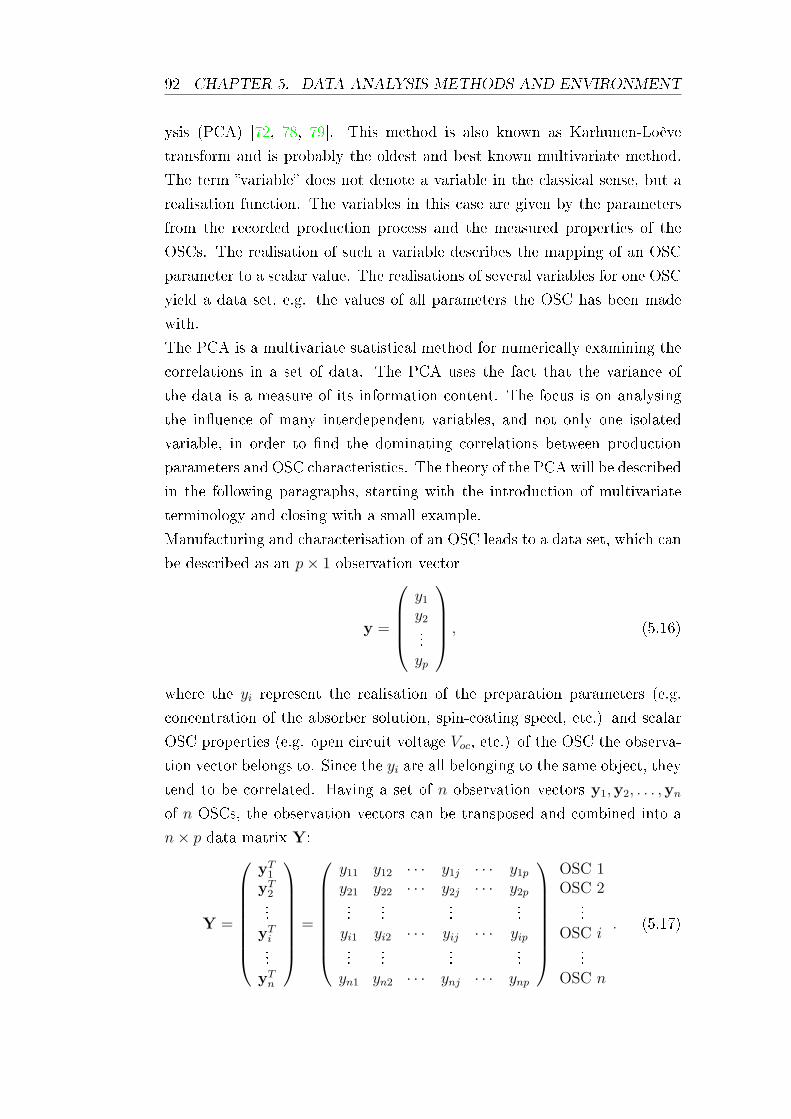
92 CHAPTER 5. DATA ANALYSIS METHODS AND ENVIRONMENT
ysis (PCA) [72, 78, 79]. This method is also known as Karhunen-Loève
transform and is probably the oldest and best known multivariate method.
The term variable does not denote a variable in the classical sense, but a
realisation function. The variables in this case are given by the parameters
from the recorded production process and the measured properties of the
OSCs. The realisation of such a variable describes the mapping of an OSC
parameter to a scalar value. The realisations of several variables for one OSC
yield a data set, e.g. the values of all parameters the OSC has been made
with.
The PCA is a multivariate statistical method for numerically examining the
correlations in a set of data. The PCA uses the fact that the variance of
the data is a measure of its information content. The focus is on analysing
the inuence of many interdependent variables, and not only one isolated
variable, in order to nd the dominating correlations between production
parameters and OSC characteristics. The theory of the PCA will be described
in the following paragraphs, starting with the introduction of multivariate
terminology and closing with a small example.
Manufacturing and characterisation of an OSC leads to a data set, which can
be described as an p× 1 observation vector
y =
y1
y2...yp
, (5.16)
where the yi represent the realisation of the preparation parameters (e.g.
concentration of the absorber solution, spin-coating speed, etc.) and scalar
OSC properties (e.g. open circuit voltage Voc, etc.) of the OSC the observa-
tion vector belongs to. Since the yi are all belonging to the same object, they
tend to be correlated. Having a set of n observation vectors y1,y2, . . . ,yn
of n OSCs, the observation vectors can be transposed and combined into a
n× p data matrix Y:
Y =
yT1
yT2...
yTi...
yTn
=
y11 y12 · · · y1j · · · y1p
y21 y22 · · · y2j · · · y2p...
......
...yi1 yi2 · · · yij · · · yip...
......
...yn1 yn2 · · · ynj · · · ynp
OSC 1OSC 2
...OSC i
...OSC n
. (5.17)
5.1. DATA ANALYSIS METHODS 93
The rst subscript represents a particular OSC, whereas the second subscript
corresponds to a particular variable. Thus one row contains the observed
values of all variables for the same OSC, whereas a column lists the values
of one variable for all OSCs. An alternative way of writing Y is using the
columns:
Y = (y(1),y(2), . . . ,y(p)), (5.18)
where e.g. y(2) is the n× 1 vector containing the observations of the second
variable on all n OSCs. This notation is useful when considering the realisa-
tion of one variable for all OSCs, e.g. for the calculation of mean or standard
deviation of a variable.
Plotting the data matrix results in a scatter plot with n data points in a
Cartesian coordinate system spanned by the p axes of the variables. The
approach of the PCA is to nd a new set of axes for the data such that the
rst new axis in the scatter plot is lying in such a way that the variance
of the data set (a measure of information content) is maximised along this
axis. The second axis is chosen to capture the second highest variance while
being orthogonal to the rst axis and so forth. All new axes are a linear
combination of the axes given by the original variables. The transformation
of the axis can be obtained as follows:
Let one data set be described by a n×p-dimensional data matrix Y as dened
in 5.17. The p× p - dimensional covariance matrix S has elements
sjk =1
n− 1
n∑i=1
(yij − y(j))(yik − y(k)) = Cov(y(j),y(k)), (5.19)
where y(j) denotes the average value of y(j), i.e. average of the jth variable.
A diagonal element sjj of S equals the variance of the jth variable.
S is symmetric and positive denite. Hence it is possible to diagonalise it
through an orthogonal transformation such that
Λ = ΓTSΓ, (5.20)
with Λ being diagonal and having the positive eigenvalues λα (α = 1, . . . , p)
of S chosen in decreasing order as diagonal entries. Since S is positive denite,
its eigenvalues are non-negative. The matrix Γ for the transformation has
the corresponding normalised eigenvectors eα as columns. The eigenvectors
are called principal component vectors (PCV), because they span the new
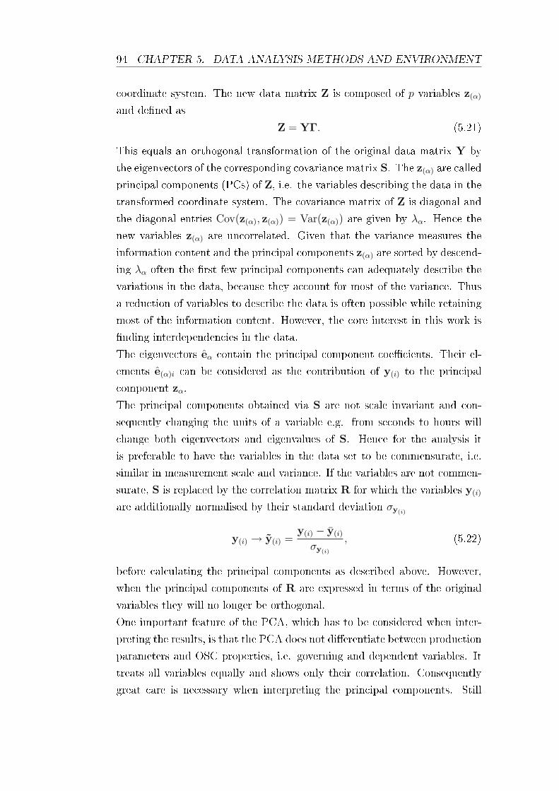
94 CHAPTER 5. DATA ANALYSIS METHODS AND ENVIRONMENT
coordinate system. The new data matrix Z is composed of p variables z(α)
and dened as
Z = YΓ. (5.21)
This equals an orthogonal transformation of the original data matrix Y by
the eigenvectors of the corresponding covariance matrix S. The z(α) are called
principal components (PCs) of Z, i.e. the variables describing the data in the
transformed coordinate system. The covariance matrix of Z is diagonal and
the diagonal entries Cov(z(α), z(α)) = Var(z(α)) are given by λα. Hence the
new variables z(α) are uncorrelated. Given that the variance measures the
information content and the principal components z(α) are sorted by descend-
ing λα often the rst few principal components can adequately describe the
variations in the data, because they account for most of the variance. Thus
a reduction of variables to describe the data is often possible while retaining
most of the information content. However, the core interest in this work is
nding interdependencies in the data.
The eigenvectors eα contain the principal component coecients. Their el-
ements e(α)i can be considered as the contribution of y(i) to the principal
component zα.
The principal components obtained via S are not scale invariant and con-
sequently changing the units of a variable e.g. from seconds to hours will
change both eigenvectors and eigenvalues of S. Hence for the analysis it
is preferable to have the variables in the data set to be commensurate, i.e.
similar in measurement scale and variance. If the variables are not commen-
surate, S is replaced by the correlation matrix R for which the variables y(i)
are additionally normalised by their standard deviation σy(i)
y(i) → y(i) =y(i) − y(i)
σy(i)
, (5.22)
before calculating the principal components as described above. However,
when the principal components of R are expressed in terms of the original
variables they will no longer be orthogonal.
One important feature of the PCA, which has to be considered when inter-
preting the results, is that the PCA does not dierentiate between production
parameters and OSC properties, i.e. governing and dependent variables. It
treats all variables equally and shows only their correlation. Consequently
great care is necessary when interpreting the principal components. Still
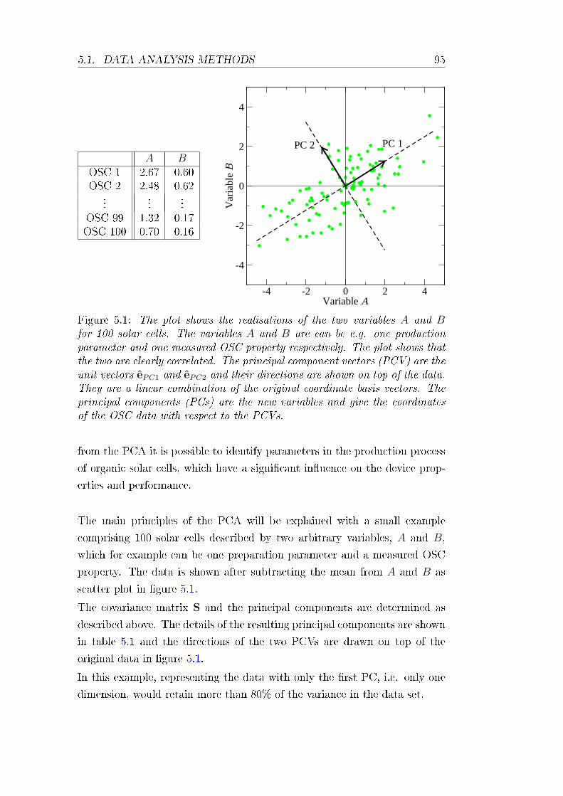
5.1. DATA ANALYSIS METHODS 95
A BOSC 1 2.67 0.60OSC 2 2.48 0.62
......
...OSC 99 1.32 -0.17OSC 100 0.70 0.16
-4 -2 0 2 4Variable A
-4
-2
0
2
4
Var
iabl
e B
PC 2 PC 1
Tue Nov 28 13:21:12 2006
Figure 5.1: The plot shows the realisations of the two variables A and Bfor 100 solar cells. The variables A and B are can be e.g. one productionparameter and one measured OSC property respectively. The plot shows thatthe two are clearly correlated. The principal component vectors (PCV) are theunit vectors ePC1 and ePC2 and their directions are shown on top of the data.They are a linear combination of the original coordinate basis vectors. Theprincipal components (PCs) are the new variables and give the coordinatesof the OSC data with respect to the PCVs.
from the PCA it is possible to identify parameters in the production process
of organic solar cells, which have a signicant inuence on the device prop-
erties and performance.
The main principles of the PCA will be explained with a small example
comprising 100 solar cells described by two arbitrary variables, A and B,
which for example can be one preparation parameter and a measured OSC
property. The data is shown after subtracting the mean from A and B as
scatter plot in gure 5.1.
The covariance matrix S and the principal components are determined as
described above. The details of the resulting principal components are shown
in table 5.1 and the directions of the two PCVs are drawn on top of the
original data in gure 5.1.
In this example, representing the data with only the rst PC, i.e. only one
dimension, would retain more than 80% of the variance in the data set.
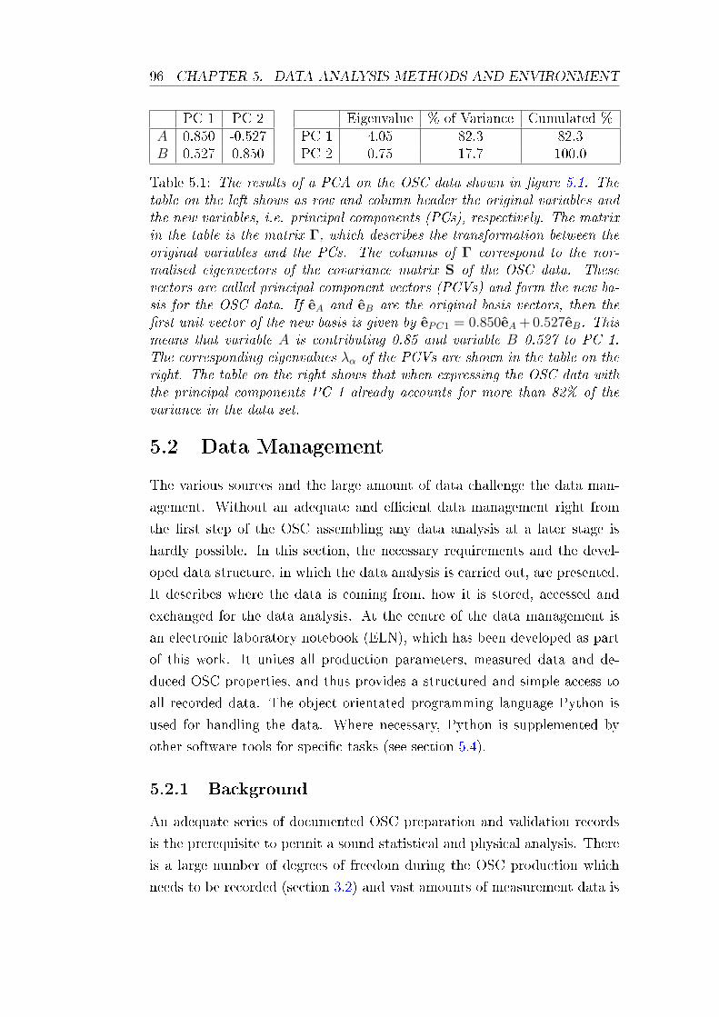
96 CHAPTER 5. DATA ANALYSIS METHODS AND ENVIRONMENT
PC 1 PC 2A 0.850 -0.527B 0.527 0.850
Eigenvalue % of Variance Cumulated %PC 1 4.05 82.3 82.3PC 2 0.75 17.7 100.0
Table 5.1: The results of a PCA on the OSC data shown in gure 5.1. Thetable on the left shows as row and column header the original variables andthe new variables, i.e. principal components (PCs), respectively. The matrixin the table is the matrix Γ, which describes the transformation between theoriginal variables and the PCs. The columns of Γ correspond to the nor-malised eigenvectors of the covariance matrix S of the OSC data. Thesevectors are called principal component vectors (PCVs) and form the new ba-sis for the OSC data. If eA and eB are the original basis vectors, then therst unit vector of the new basis is given by ePC1 = 0.850eA + 0.527eB. Thismeans that variable A is contributing 0.85 and variable B 0.527 to PC 1.The corresponding eigenvalues λα of the PCVs are shown in the table on theright. The table on the right shows that when expressing the OSC data withthe principal components PC 1 already accounts for more than 82% of thevariance in the data set.
5.2 Data Management
The various sources and the large amount of data challenge the data man-
agement. Without an adequate and ecient data management right from
the rst step of the OSC assembling any data analysis at a later stage is
hardly possible. In this section, the necessary requirements and the devel-
oped data structure, in which the data analysis is carried out, are presented.
It describes where the data is coming from, how it is stored, accessed and
exchanged for the data analysis. At the centre of the data management is
an electronic laboratory notebook (ELN), which has been developed as part
of this work. It unites all production parameters, measured data and de-
duced OSC properties, and thus provides a structured and simple access to
all recorded data. The object orientated programming language Python is
used for handling the data. Where necessary, Python is supplemented by
other software tools for specic tasks (see section 5.4).
5.2.1 Background
An adequate series of documented OSC preparation and validation records
is the prerequisite to permit a sound statistical and physical analysis. There
is a large number of degrees of freedom during the OSC production which
needs to be recorded (section 3.2) and vast amounts of measurement data is
5.2. DATA MANAGEMENT 97
obtained through the automation of the main OSC characterisation methods
(chapter 4). As the eects of parameter variations on the properties of an
OSC are usually not attributable to one particular variation, the complete
history of an OSC has to be considered when interpreting the results of the
characterisation. Furthermore, the data has to be managed in a way, which
allows easy and reliable handling.
So far, the details of preparation steps had been recorded in each group
member's paper-based laboratory book. The entries were written in individ-
ual styles and a general access to this information was dicult. Similarly,
measured data was generated in dierent experimental setups with dierent
conventions of storing the data, in many cases even without information on
what the raw data represented in a data le. However, an easy and reliable
access to both kinds of information is a key component for a systematic anal-
ysis. For this reason, a central repository was created, where all data, from
production processes up to the deduced OSC properties, is stored in detail
in a structured and standardised way. This central data repository is called
electronic laboratory notebook (ELN). It constitutes the data base on which
the data analysis is built.
5.2.2 Data Acquisition and Data Flow
The data for the analysis is coming from two main sources:
• Parameters from the OSC production process
• Data from the OSC characterisation
Additionally there is auxiliary data with e.g. important material constants
or device settings, which complement OSC preparation parameters and mea-
surement data. Various types of data have to be managed and despite their
dierent sources, all data is gathered and integrated into one central struc-
ture, the ELN.
Manufacturing Data
During the OSC production process, the recording of the various dierent
process steps and their parameters (see section 3.2) is necessary. Starting
with paper-based route cards to standardise the OSC preparation parame-
ters, the whole recording of the production was moved directly to an elec-
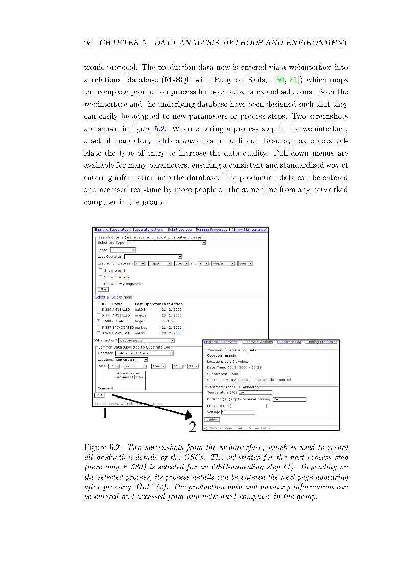
98 CHAPTER 5. DATA ANALYSIS METHODS AND ENVIRONMENT
tronic protocol. The production data now is entered via a webinterface into
a relational database (MySQL with Ruby on Rails, [80, 81]) which maps
the complete production process for both substrates and solutions. Both the
webinterface and the underlying database have been designed such that they
can easily be adapted to new parameters or process steps. Two screenshots
are shown in gure 5.2. When entering a process step in the webinterface,
a set of mandatory elds always has to be lled. Basic syntax checks val-
idate the type of entry to increase the data quality. Pull-down menus are
available for many parameters, ensuring a consistent and standardised way of
entering information into the database. The production data can be entered
and accessed real-time by more people at the same time from any networked
computer in the group.
Figure 5.2: Two screenshots from the webinterface, which is used to recordall production details of the OSCs. The substrates for the next process step(here only F 580) is selected for an OSC-annealing step (1). Depending onthe selected process, its process details can be entered the next page appearingafter pressing Go! (2). The production data and auxiliary information canbe entered and accessed from any networked computer in the group.
5.2. DATA MANAGEMENT 99
The MySQL-database also handles all auxiliary information necessary dur-
ing production. This includes details e.g. on the materials available for the
absorber solutions and for evaporation, as well as the settings of the equip-
ment, e.g. speed proles of the spin-coating programs. All this can also be
accessed and maintained through the same webinterface.
The measurement data from the characterisation is not included in the
MySQL-database. When handling experimental data of various kinds, a re-
lational database has several shortcomings, e.g. information on the measured
data has to be stored separately from the raw data and the queries for retriev-
ing data can become very complex. However, for recording the production
parameters through an user-friendly webinterface, the MySQL-database with
Ruby on Rails was the quickest realisable and most pragmatic solution for
moving from a paper based to an electronic protocol. The relational database
now replaces paper based notes in the laboratory for the standard processes
making instead all information available in electronic form, accessible from
any computer in the group.
Because the measured data would be separate from the production data, the
MySQL-database therefore is only an intermediate step on the way to com-
bining all necessary data. The subsequent data transfer from the MySQL-
database to the ELN is done via the extended markup language (XML, [82]).
XML is a platform independent general purpose markup language, which
makes XML very exible and powerful for data exchange between dierent
systems.
Measurement Data
The second major source of data is the measurement data. Prior to the au-
tomation of the main characterisation methods (section 4.2), measured data
had been stored dierently for every measurement method. The output les
then generally only contained raw data without extra information, making
the attribution of a data le to a particular measurement and OSC often
dicult.
The standard measurements are now all controlled by one central LabView
program described in section 4.2.4, which stores the measured data in a
standardised way independent of the actual measurement method. However,
the used LabView version (7.0) so far lacks sucient support for writing its
output les directly as XML les [82], which would have been the best way to
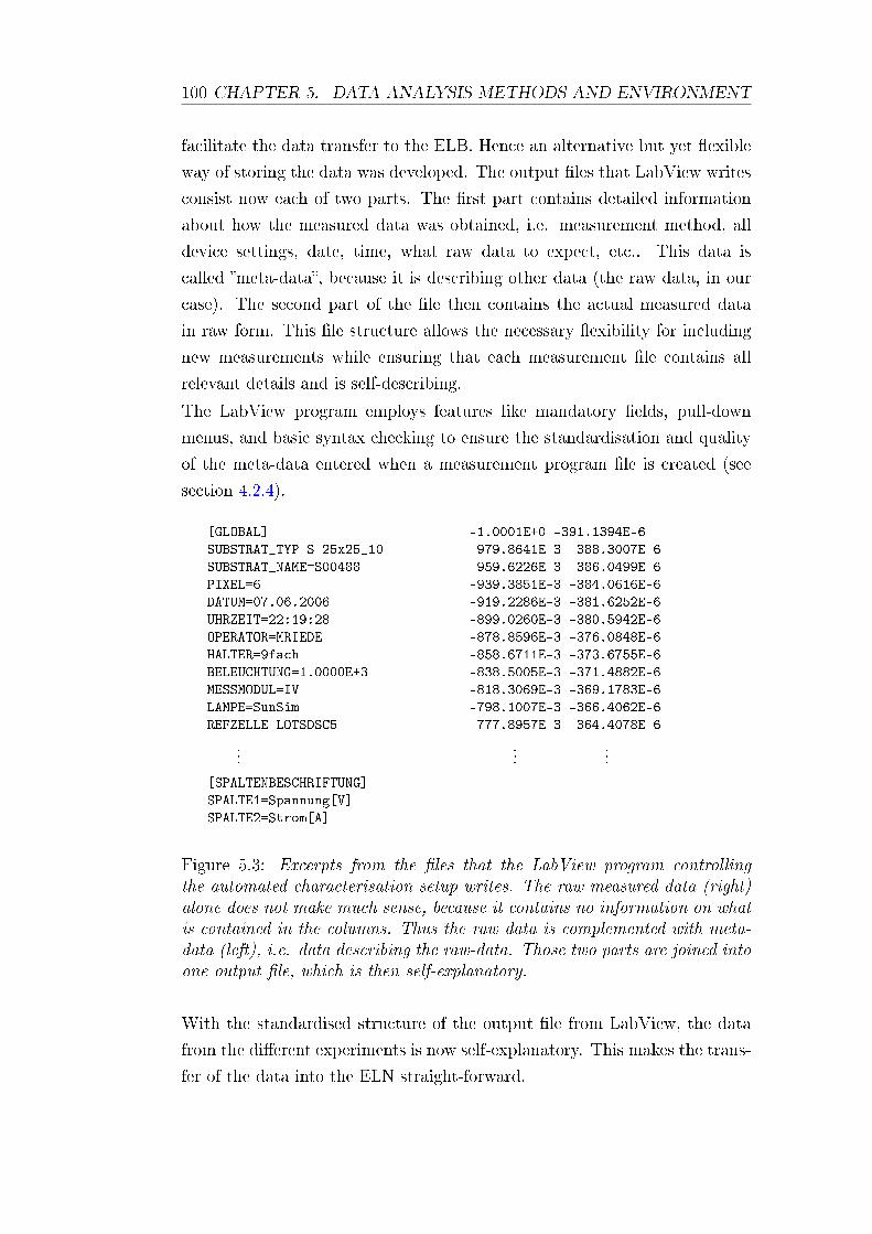
100 CHAPTER 5. DATA ANALYSIS METHODS AND ENVIRONMENT
facilitate the data transfer to the ELB. Hence an alternative but yet exible
way of storing the data was developed. The output les that LabView writes
consist now each of two parts. The rst part contains detailed information
about how the measured data was obtained, i.e. measurement method, all
device settings, date, time, what raw data to expect, etc.. This data is
called meta-data, because it is describing other data (the raw data, in our
case). The second part of the le then contains the actual measured data
in raw form. This le structure allows the necessary exibility for including
new measurements while ensuring that each measurement le contains all
relevant details and is self-describing.
The LabView program employs features like mandatory elds, pull-down
menus, and basic syntax checking to ensure the standardisation and quality
of the meta-data entered when a measurement program le is created (see
section 4.2.4).
[GLOBAL]
SUBSTRAT_TYP=S-25x25_10
SUBSTRAT_NAME=S00488
PIXEL=6
DATUM=07.06.2006
UHRZEIT=22:19:28
OPERATOR=MRIEDE
HALTER=9fach
BELEUCHTUNG=1.0000E+3
MESSMODUL=IV
LAMPE=SunSim
REFZELLE=LOTSDSC5
...
[SPALTENBESCHRIFTUNG]
SPALTE1=Spannung[V]
SPALTE2=Strom[A]
-1.0001E+0 -391.1394E-6
-979.8641E-3 -388.3007E-6
-959.6226E-3 -386.0499E-6
-939.3851E-3 -384.0616E-6
-919.2286E-3 -381.6252E-6
-899.0260E-3 -380.5942E-6
-878.8596E-3 -376.0848E-6
-858.6711E-3 -373.6755E-6
-838.5005E-3 -371.4882E-6
-818.3069E-3 -369.1783E-6
-798.1007E-3 -366.4062E-6
-777.8957E-3 -364.4078E-6
......
Figure 5.3: Excerpts from the les that the LabView program controllingthe automated characterisation setup writes. The raw measured data (right)alone does not make much sense, because it contains no information on whatis contained in the columns. Thus the raw data is complemented with meta-data (left), i.e. data describing the raw-data. Those two parts are joined intoone output le, which is then self-explanatory.
With the standardised structure of the output le from LabView, the data
from the dierent experiments is now self-explanatory. This makes the trans-
fer of the data into the ELN straight-forward.
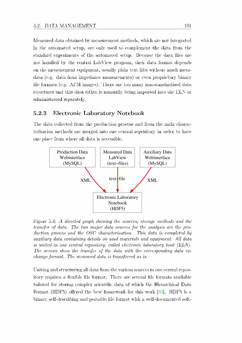
5.2. DATA MANAGEMENT 101
Measured data obtained by measurement methods, which are not integrated
in the automated setup, are only used to complement the data from the
standard experiments of the automated setup. Because the data les are
not handled by the central LabView program, their data format depends
on the measurement equipment, usually plain text les without much meta-
data (e.g. data from impedance measurements) or even proprietary binary
le formats (e.g. AFM images). There are too many non-standardised data
structures and this data either is manually being imported into the ELN or
administrated separately.
5.2.3 Electronic Laboratory Notebook
The data collected from the production process and from the main charac-
terisation methods are merged into one central repository in order to have
one place from where all data is accessible.
Webinterface
(MySQL)
Electronic Laboratory
Notebook
LabView
(text−files)
Auxiliary Data
(MySQL)
XMLXML
Measured Data
(HDF5)
text−file
Production Data
Webinterface
Figure 5.4: A directed graph showing the sources, storage methods and thetransfer of data. The two major data sources for the analysis are the pro-duction process and the OSC characterisation. This data is completed byauxiliary data containing details on used materials and equipment. All datais united in one central repository, called electronic laboratory book (ELN).The arrows show the transfer of the data with the corresponding data ex-change format. The measured data is transferred as is.
Uniting and structuring all data from the various sources in one central repos-
itory requires a exible le format. There are several le formats available
tailored for storing complex scientic data of which the Hierarchical Data
Format (HDF5) oered the best framework for this work [83]. HDF5 is a
binary, self-describing and portable le format with a well-documented soft-
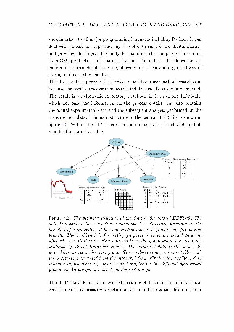
102 CHAPTER 5. DATA ANALYSIS METHODS AND ENVIRONMENT
ware interface to all major programming languages including Python. It can
deal with almost any type and any size of data suitable for digital storage
and provides the largest exibility for handling the complex data coming
from OSC production and characterisation. The data in the le can be or-
ganised in a hierarchical structure, allowing for a clear and organised way of
storing and accessing the data.
This data-centric approach for the electronic laboratory notebook was chosen,
because changes in processes and associated data can be easily implemented.
The result is an electronic laboratory notebook in form of one HDF5-le,
which not only has information on the process details, but also contains
the actual experimental data and the subsequent analysis performed on the
measurement data. The main structure of the central HDF5 le is shown in
gure 5.5. Within the ELN, there is a continuous track of each OSC and all
modications are traceable.
2−D Arrays
300 400 500 600 700 800Wavelength / nm
0
0.25
0.5
0.75
1
Ab
sorp
tio
n
Absorption non-anneald (nan)
Absorption annealed (an)
Sat Nov 25 10:44:56 2006
Tables, e.g Spin−coating Programs.:
Tables, e.g Substrate Log.: Tables, e.g. IV−Analysis:
’/’ (root)
Measued Data
Workbench
ELB Analysis
Auxiliary Data
Figure 5.5: The primary structure of the data in the central HDF5-le Thedata is organised in a structure comparable to a directory structure on theharddisk of a computer. It has one central root node from where ve groupsbranch. The workbench is for testing purposes to leave the actual data un-aected. The ELB is the electronic log base, the group where the electronicprotocols of all substrates are stored. The measured data is stored in self-describing arrays in the data group. The analysis group contains tables withthe parameters extracted from the measured data. Finally, the auxiliary dataprovides information e.g. on the speed proles for the dierent spin-coaterprograms. All groups are linked via the root group.
The HDF5 data denition allows a structuring of its content in a hierarchical
way, similar to a directory structure on a computer, starting from one root
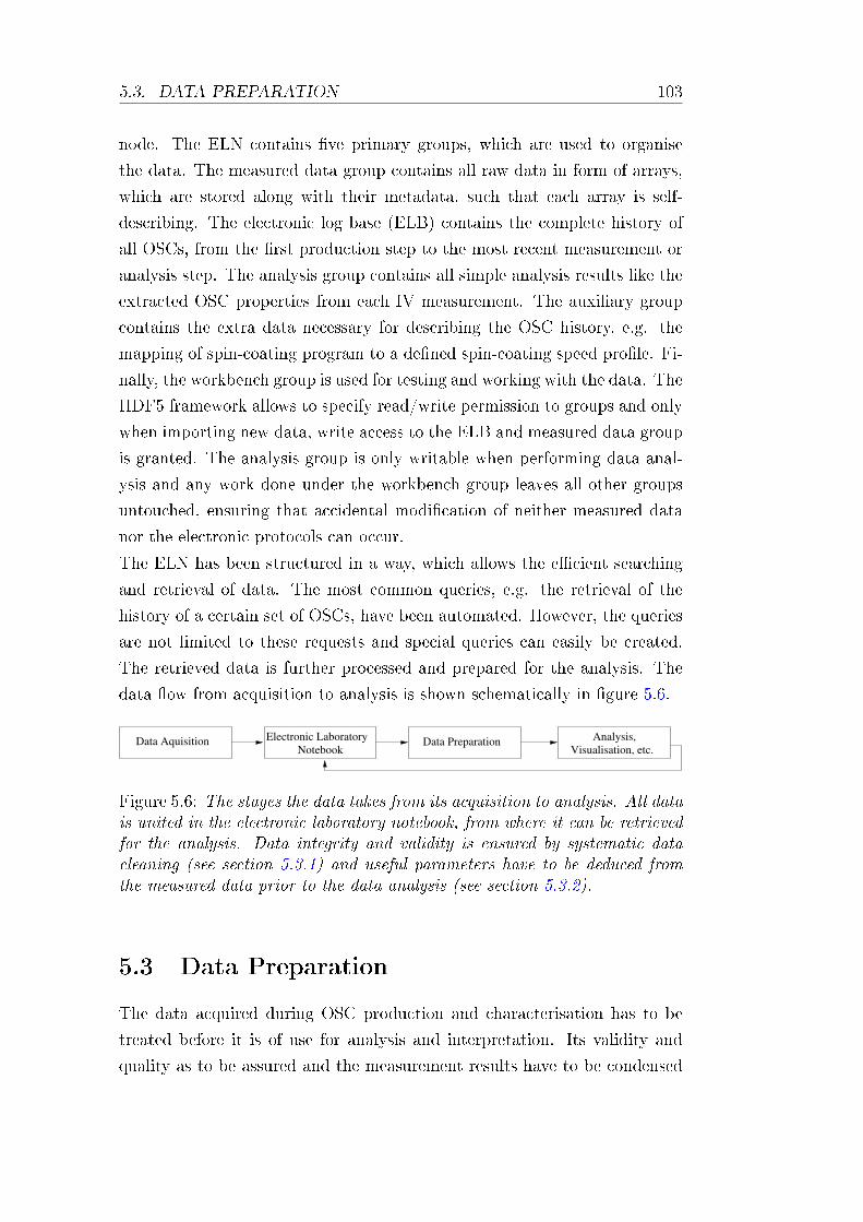
5.3. DATA PREPARATION 103
node. The ELN contains ve primary groups, which are used to organise
the data. The measured data group contains all raw data in form of arrays,
which are stored along with their metadata, such that each array is self-
describing. The electronic log base (ELB) contains the complete history of
all OSCs, from the rst production step to the most recent measurement or
analysis step. The analysis group contains all simple analysis results like the
extracted OSC properties from each IV measurement. The auxiliary group
contains the extra data necessary for describing the OSC history, e.g. the
mapping of spin-coating program to a dened spin-coating speed prole. Fi-
nally, the workbench group is used for testing and working with the data. The
HDF5 framework allows to specify read/write permission to groups and only
when importing new data, write access to the ELB and measured data group
is granted. The analysis group is only writable when performing data anal-
ysis and any work done under the workbench group leaves all other groups
untouched, ensuring that accidental modication of neither measured data
nor the electronic protocols can occur.
The ELN has been structured in a way, which allows the ecient searching
and retrieval of data. The most common queries, e.g. the retrieval of the
history of a certain set of OSCs, have been automated. However, the queries
are not limited to these requests and special queries can easily be created.
The retrieved data is further processed and prepared for the analysis. The
data ow from acquisition to analysis is shown schematically in gure 5.6.
Analysis,Visualisation, etc.
Electronic LaboratoryNotebook
Data Aquisition Data Preparation
Figure 5.6: The stages the data takes from its acquisition to analysis. All datais united in the electronic laboratory notebook, from where it can be retrievedfor the analysis. Data integrity and validity is ensured by systematic datacleaning (see section 5.3.1) and useful parameters have to be deduced fromthe measured data prior to the data analysis (see section 5.3.2).
5.3 Data Preparation
The data acquired during OSC production and characterisation has to be
treated before it is of use for analysis and interpretation. Its validity and
quality as to be assured and the measurement results have to be condensed
104 CHAPTER 5. DATA ANALYSIS METHODS AND ENVIRONMENT
into a format useful for the further analysis. These steps are described in the
following sections.
5.3.1 Data Cleaning
Checking the quality of the data and the associated correction and pruning is
usually called data cleaning. The data in this work consists of two main com-
ponents: the production parameters and the measurement results. Whereas
for the production parameters human errors, i.e. wrong entries in the ELN,
need to be corrected, the measured data has additionally to be checked for
artefacts from the measurements. Data cleaning is an essential cornerstone
for a reliable data analysis and this section is intended to describe how the
data cleaning is carried out in order to obtain a consistent and reliable base
of data for the analysis.
Manufacturing Data
The webinterface, through which the details of production for each substrate
are entered, already provides important measures for assuring data consis-
tency, completeness and quality. The use of mandatory elds and syntax
checking ensures that e.g. if a temperature is required, it has to entered nu-
merically. Similarly, pull-down menus limit the options to sensible choices for
certain parameters, e.g. oering only valid spin-coating programs. However,
these mechanisms cannot safeguard against all mistakes and these errors need
to be found and corrected before the data is used for the analysis. If a param-
eter in question is found, e.g. unreasonable long or negative time intervals
between production steps, one must resolve the issue with the person who
entered the data. If in doubt, the parameter is either set to a value indicating
unknown or the whole corresponding data set for the substrate is exempt
from the analysis requiring the parameter.
Measured Data
To ensure the quality of the OSCs, all are already visually inspected for dam-
ages and defects in the photovoltaic active region during production. Often a
particular behaviour in the measured data is not caused by variations in the
production process, but by such defects. This measurement data, together
with measurement data, which is obviously awed due other reasons, has to
5.3. DATA PREPARATION 105
be treated separately in order to obtain a useful set of data for the analysis.
To describe and quantify the cases, in which an OSC is not considered for
the analysis, they have been categorised as follows:
• OSCs with only partial coverage of absorber layer
• Defects due to bubbles during spin-coating of the absorber layer
• Scratches in the absorber layer and Al-cathode caused by handling
• Particles in the absorber layer from dust or agglomerates
• Contact Problems
• Unspecied
Figure 5.7 shows the eect of these defects on the illuminated IV-curves
and absorption measurement as well as corresponding pictures. The degree
to which they aect the measurements varies and generally depends on the
extent of the defect. The primary causes of the above mentioned defects are
briey discussed here.
The PEDOT:PSS layer is very homogeneous and covers the whole substrate
area. Hence, if the area of an OSC is only partially covered during the sub-
sequent spin-coating with the absorber layer, the aluminium cathode has
direct contact to the PEDOT:PSS layer. The extent of the S-shaped IV-
curve depends on the overlap area of the PEDOT:PSS|aluminium contact.
The PEDOT:PSS|aluminium is creating a Schottky-like contact, while the
area covered with absorber layer (if any) still generates photocurrent (see
gure 5.7 A). An only partially covered OSC also aects the absorption mea-
surement. In the region without absorber layer most of the light is reected,
leading to a dierent spectrum due to a missing layer (see gure 5.7 B).
Whereas bubbles have never been observed in the PEDOT:PSS layer, bubbles
in the absorber layer can occasionally be created during the spin-coating of
the absorber solution. While spinning the substrate, the bubble distorts
the otherwise smooth lm and can lead to a very inhomogeneous absorber
layer. This inhomogeneity in thickness often aects more than one OSC per
substrate, because of the comparably large size of bubbles. Bubbles cause
S-shaped IV-curves as shown in gure 5.7 A and appear in the absorption
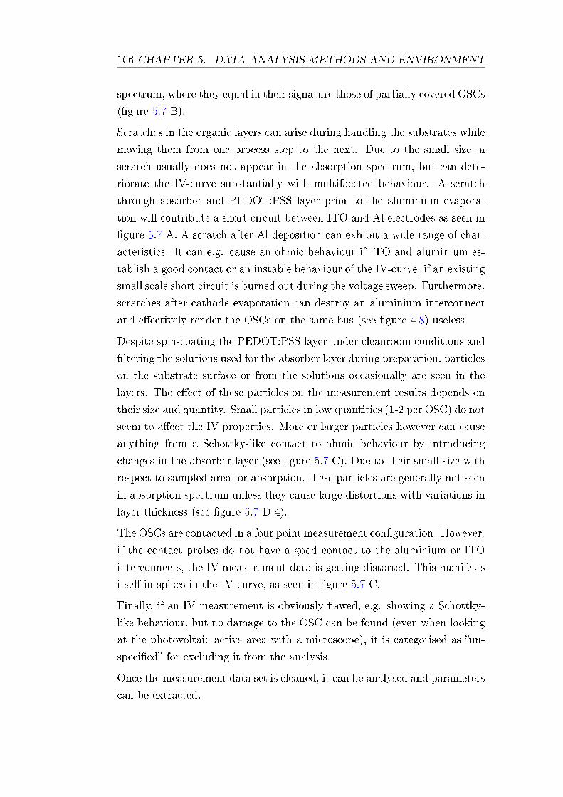
106 CHAPTER 5. DATA ANALYSIS METHODS AND ENVIRONMENT
spectrum, where they equal in their signature those of partially covered OSCs
(gure 5.7 B).
Scratches in the organic layers can arise during handling the substrates while
moving them from one process step to the next. Due to the small size, a
scratch usually does not appear in the absorption spectrum, but can dete-
riorate the IV-curve substantially with multifaceted behaviour. A scratch
through absorber and PEDOT:PSS layer prior to the aluminium evapora-
tion will contribute a short circuit between ITO and Al electrodes as seen in
gure 5.7 A. A scratch after Al-deposition can exhibit a wide range of char-
acteristics. It can e.g. cause an ohmic behaviour if ITO and aluminium es-
tablish a good contact or an instable behaviour of the IV-curve, if an existing
small scale short circuit is burned out during the voltage sweep. Furthermore,
scratches after cathode evaporation can destroy an aluminium interconnect
and eectively render the OSCs on the same bus (see gure 4.8) useless.
Despite spin-coating the PEDOT:PSS layer under cleanroom conditions and
ltering the solutions used for the absorber layer during preparation, particles
on the substrate surface or from the solutions occasionally are seen in the
layers. The eect of these particles on the measurement results depends on
their size and quantity. Small particles in low quantities (1-2 per OSC) do not
seem to aect the IV properties. More or larger particles however can cause
anything from a Schottky-like contact to ohmic behaviour by introducing
changes in the absorber layer (see gure 5.7 C). Due to their small size with
respect to sampled area for absorption, these particles are generally not seen
in absorption spectrum unless they cause large distortions with variations in
layer thickness (see gure 5.7 D 4).
The OSCs are contacted in a four point measurement conguration. However,
if the contact probes do not have a good contact to the aluminium or ITO
interconnects, the IV measurement data is getting distorted. This manifests
itself in spikes in the IV-curve, as seen in gure 5.7 C.
Finally, if an IV measurement is obviously awed, e.g. showing a Schottky-
like behaviour, but no damage to the OSC can be found (even when looking
at the photovoltaic active area with a microscope), it is categorised as un-
specied for excluding it from the analysis.
Once the measurement data set is cleaned, it can be analysed and parameters
can be extracted.
5.3. DATA PREPARATION 107
-1 -0.5 0 0.5 1Voltage / V
-1000
0
1000C
urre
nt D
ensi
ty /
mA
/cm
2
S 421 p3 (normal)S 413 p6 (not covered)S 423 p8 (scratch)S 452 p1 (with bubble)
A
illuminated IV-curves
Tue Jul 25 20:07:14 2006
300 400 500 600 700 800Wavelength / nm
0.0
0.2
0.4
0.6
0.8
1.0
Abs
orpt
ion
S 413 p6 (only partially covered)S 413 all without p9
B
Absorption Measurement
-1 -0.5 0 0.5 1Voltage / V
0
50
100
Cur
rent
Den
sity
/ m
A/c
m2
S 423 p6 (normal)S 451 p1 (with particles)S 419 p10 (contact problems)
C
illuminated IV-curves
Figure 5.7: The categorisation of measurement data upon pruning prior to thedata analysis. (A) shows the eects on IV-curves when the OSC is not com-pletely covered with the absorber layer, a bubble during spin-coating causesstrong inhomogeneities in the absorber layer or a scratch creates a short cir-cuit. Signatures in the absorption spectrum of a bubble and a partially coveredOSC are similar and the example of a non-covered OSC is shown in (B). (C)shows an S-shaped IV-curve causes by several particles in the photovoltaicactive region and contacting problems. In (D) pictures of the four cases il-lustrated above are shown: no coverage with absorber (1), scratches in thecathode (2), inhomogeneities caused by a bubble during spin-coating (3) anda large particle (4).
5.3.2 Extraction of OSC Properties fromMeasured Data
Most measurements used in this work yield two-dimensional curves. The
information contained in these curves has to be extracted by condensing
the measured data into a set of meaningful scalar OSC properties. Some
properties can be directly read from a measured curve, others have to be de-
termined by tting functions or suitable models to the curve. The following
sections describe how the data of the main measurements was treated and
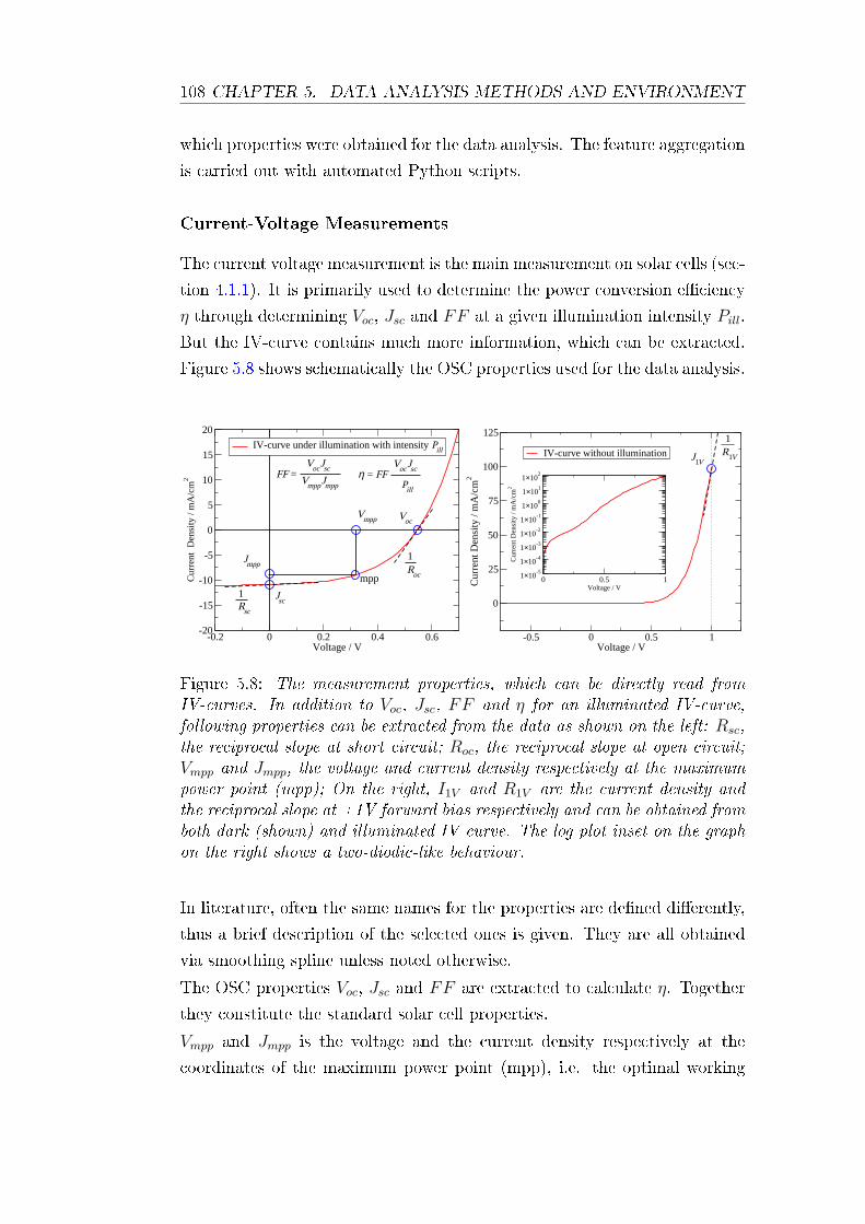
108 CHAPTER 5. DATA ANALYSIS METHODS AND ENVIRONMENT
which properties were obtained for the data analysis. The feature aggregation
is carried out with automated Python scripts.
Current-Voltage Measurements
The current voltage measurement is the main measurement on solar cells (sec-
tion 4.1.1). It is primarily used to determine the power conversion eciency
η through determining Voc, Jsc and FF at a given illumination intensity Pill.
But the IV-curve contains much more information, which can be extracted.
Figure 5.8 shows schematically the OSC properties used for the data analysis.
-0.2 0 0.2 0.4 0.6Voltage / V
-20
-15
-10
-5
0
5
10
15
20
Cur
rent
Den
sity
/ m
A/c
m2
IV-curve under illumination with intensity Pill
Voc
Jsc
Jmpp
Vmpp
Roc
Rsc
1
1
η = FFVocJsc
Pill
mpp
FF = VocJsc
VmppJmpp
Tue Nov 28 13:32:59 2006
-0.5 0 0.5 1Voltage / V
0
25
50
75
100
125
Cur
rent
Den
sity
/ m
A/c
m2
IV-curve without illumination
0 0.5 1Voltage / V
1×10⁻⁵
1×10⁻⁴
1×10⁻³
1×10⁻²
1×10⁻¹
1×100
1×101
1×10²
Cur
rent
Den
sity
/ m
A/c
m2
1R
1VJ1V
Sat Nov 25 10:59:13 2006
Figure 5.8: The measurement properties, which can be directly read fromIV-curves. In addition to Voc, Jsc, FF and η for an illuminated IV-curve,following properties can be extracted from the data as shown on the left: Rsc,the reciprocal slope at short circuit; Roc, the reciprocal slope at open circuit;Vmpp and Jmpp, the voltage and current density respectively at the maximumpower point (mpp); On the right, I1V and R1V are the current density andthe reciprocal slope at +1V forward bias respectively and can be obtained fromboth dark (shown) and illuminated IV-curve. The log-plot inset on the graphon the right shows a two-diodic-like behaviour.
In literature, often the same names for the properties are dened dierently,
thus a brief description of the selected ones is given. They are all obtained
via smoothing spline unless noted otherwise.
The OSC properties Voc, Jsc and FF are extracted to calculate η. Together
they constitute the standard solar cell properties.
Vmpp and Jmpp is the voltage and the current density respectively at the
coordinates of the maximum power point (mpp), i.e. the optimal working
5.3. DATA PREPARATION 109
point for a solar cell. Its value is obtained during the same procedure as Voc,
Jsc and FF .
In addition to these properties, there are further properties, which are of
interest when analysing the behaviour of organic solar cells. Rsc is the recip-
rocal slope at short circuit, i.e. ∂V∂J
∣∣V =0V
. It might be related to the series
resistance Rs. In amorphous silicon solar cells, Rsc is sometimes used to de-
termine further properties of the solar cell, e.g. the built-in potential Vbi [50].
Roc, the reciprocal slope at open circuit, i.e. ∂V∂J
∣∣V =Voc
. It might be related
to the parallel resistance Rp.
R1V is the reciprocal slope at 1V forward bias, i.e. ∂V∂J
∣∣V =1V
. It should be
a measure of how good the interfaces can inject charges into the bulk of
the OSC. R1V is obtained via linear regression, because splines can under
certain circumstances start to oscillate at the boundaries. In literature R1V
is sometimes called Rs, which however can really only be obtained by tting
a suitable model to the curve. Finally, J1V , the current at 1V forward bias
may be a measure of Rs.
The log-plot of a dark IV-curve as shown as inset in gure 5.8 on the right-
hand side is currently investigated. Fitting numerically a two-diode model
does not yield an adequate t. The log-plots of dierent OSCs show a distinct
dierent behaviour and the origins are subject to ongoing research.
Further properties can be deduced from the IV-curve by tting a model func-
tion to the data. The simple diode equation 5.23 (repeated from section 2.4.2)
is tted with the Levenberg-Marquardt Algorithm (LMA, section 5.1.2) to
the data. For good OSCs, good ts can be achieved with this model function
(see gure 5.9 left). However, it is not possible with this model to reproduce,
e.g. the kink of the IV-curve in the fourth quadrant (see gure 5.9 right),
which is often observed.
I − I01
(exp
(e(V − IRs)
n1kBT
)− 1
)− V − IRs
Rp
+ Iph = 0, (5.23)
where I01 is the dark saturation current, n1 the diode ideality factor, Iph the
photogenerated current and Rs and Rp the serial and parallel resistances.
The equivalent circuit model was shown in section 2.4.2.
Absorption Measurements
The results from the absorption measurements (section 4.1.3) are used for
both assessing the quality of the spin-coated layers and calculating the ab-
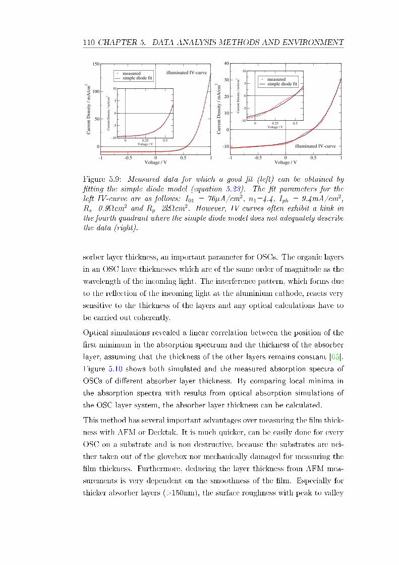
110 CHAPTER 5. DATA ANALYSIS METHODS AND ENVIRONMENT
-1 -0.5 0 0.5 1Voltage / V
0
50
100
150
Cur
rent
Den
sity
/ m
A/c
m2
measuredsimple diode fit
0 0.25 0.5Voltage / V
-10
-5
0
5
10
Cur
rent
Den
sity
/ m
A/c
m2
illuminated IV-curve
Thu Jul 27 21:53:43 2006
-1 -0.5 0 0.5 1Voltage / V
-10
0
10
20
30
40
Cur
rent
Den
sity
/ m
A/c
m2
0 0.25 0.5Voltage / V
-10
-5
0
5
10
Cur
rent
Den
sity
/ m
A/c
m2 measured
simple diode fit
illuminated IV-curve
Thu Jul 27 22:11:21 2006
Figure 5.9: Measured data for which a good t (left) can be obtained bytting the simple diode model (equation 5.23). The t parameters for theleft IV-curve are as follows: I01 = 76µA/cm2, n1=4.4, Iph = 9.4mA/cm2,Rs=0.9Ωcm
2 and Rp=2kΩcm2. However, IV-curves often exhibit a kink in
the fourth quadrant where the simple diode model does not adequately describethe data (right).
sorber layer thickness, an important parameter for OSCs. The organic layers
in an OSC have thicknesses which are of the same order of magnitude as the
wavelength of the incoming light. The interference pattern, which forms due
to the reection of the incoming light at the aluminium cathode, reacts very
sensitive to the thickness of the layers and any optical calculations have to
be carried out coherently.
Optical simulations revealed a linear correlation between the position of the
rst minimum in the absorption spectrum and the thickness of the absorber
layer, assuming that the thickness of the other layers remains constant [65].
Figure 5.10 shows both simulated and the measured absorption spectra of
OSCs of dierent absorber layer thickness. By comparing local minima in
the absorption spectra with results from optical absorption simulations of
the OSC layer system, the absorber layer thickness can be calculated.
This method has several important advantages over measuring the lm thick-
ness with AFM or Decktak. It is much quicker, can be easily done for every
OSC on a substrate and is non destructive, because the substrates are nei-
ther taken out of the glovebox nor mechanically damaged for measuring the
lm thickness. Furthermore, deducing the layer thickness from AFM mea-
surements is very dependent on the smoothness of the lm. Especially for
thicker absorber layers (>150nm), the surface roughness with peak to valley
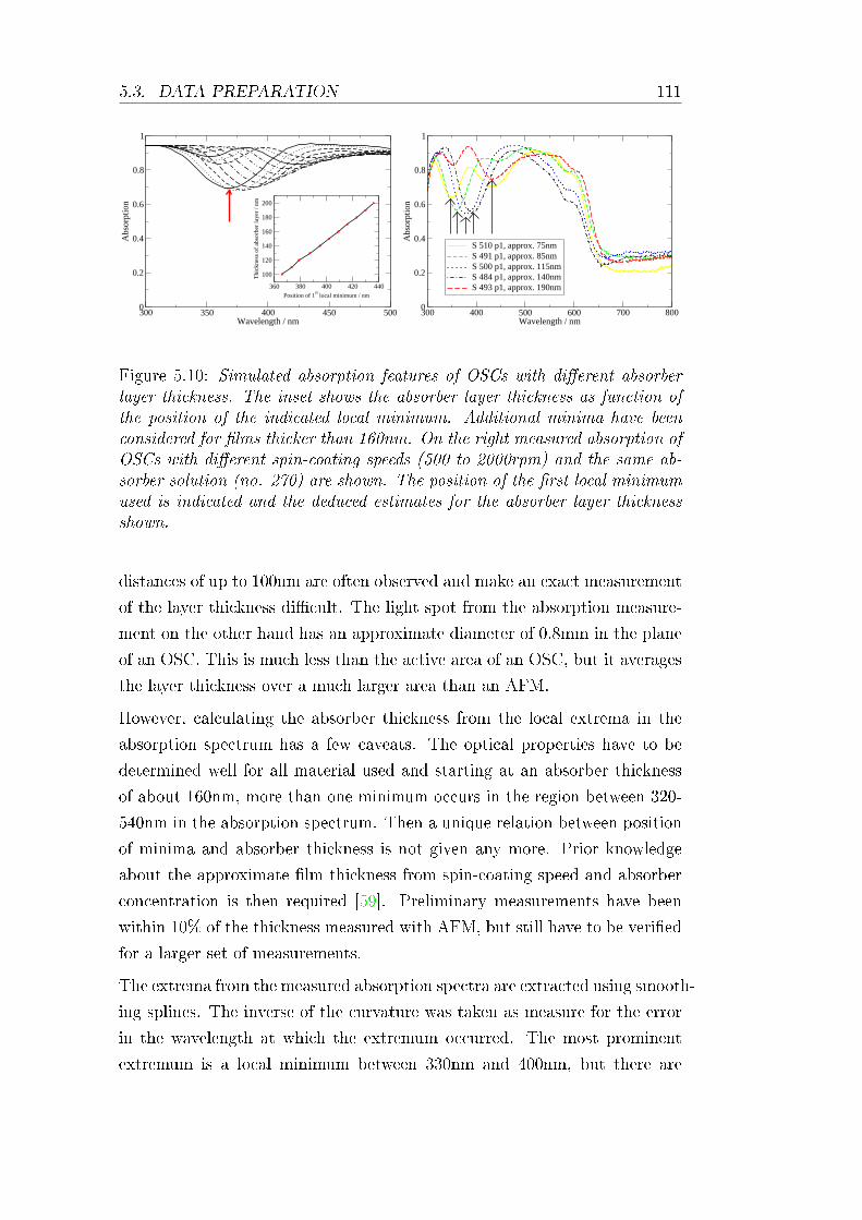
5.3. DATA PREPARATION 111
300 350 400 450 500Wavelength / nm
0
0.2
0.4
0.6
0.8
1
Abs
orpt
ion
360 380 400 420 440Position of 1
st local minimum / nm
100
120
140
160
180
200
Thi
ckne
ss o
f ab
sorb
er la
yer
/ nm
Sat Nov 25 11:01:23 2006
300 400 500 600 700 800Wavelength / nm
0
0.2
0.4
0.6
0.8
1
Abs
orpt
ion
S 510 p1, approx. 75nmS 491 p1, approx. 85nmS 500 p1, approx. 115nmS 484 p1, approx. 140nmS 493 p1, approx. 190nm
Sat Nov 25 11:02:11 2006
Figure 5.10: Simulated absorption features of OSCs with dierent absorberlayer thickness. The inset shows the absorber layer thickness as function ofthe position of the indicated local minimum. Additional minima have beenconsidered for lms thicker than 160nm. On the right measured absorption ofOSCs with dierent spin-coating speeds (500 to 2000rpm) and the same ab-sorber solution (no. 270) are shown. The position of the rst local minimumused is indicated and the deduced estimates for the absorber layer thicknessshown.
distances of up to 100nm are often observed and make an exact measurement
of the layer thickness dicult. The light spot from the absorption measure-
ment on the other hand has an approximate diameter of 0.8mm in the plane
of an OSC. This is much less than the active area of an OSC, but it averages
the layer thickness over a much larger area than an AFM.
However, calculating the absorber thickness from the local extrema in the
absorption spectrum has a few caveats. The optical properties have to be
determined well for all material used and starting at an absorber thickness
of about 160nm, more than one minimum occurs in the region between 320-
540nm in the absorption spectrum. Then a unique relation between position
of minima and absorber thickness is not given any more. Prior knowledge
about the approximate lm thickness from spin-coating speed and absorber
concentration is then required [59]. Preliminary measurements have been
within 10% of the thickness measured with AFM, but still have to be veried
for a larger set of measurements.
The extrema from the measured absorption spectra are extracted using smooth-
ing splines. The inverse of the curvature was taken as measure for the error
in the wavelength at which the extremum occurred. The most prominent
extremum is a local minimum between 330nm and 400nm, but there are
112 CHAPTER 5. DATA ANALYSIS METHODS AND ENVIRONMENT
typically more extrema, which can be used for calculating and conrming
the absorber layer thickness. The rst four prominent extrema are usually
extracted.
Spectral Response Measurements
The EQE and SR curves obtained from the spectral response measurement
can currently only be used qualitatively. For the last few months, during
which the experiments were carried out, it was not possible to reconcile the
results of the JSRsc calculated from the SR (section 4.1.2) and the Jsc from
the IV-measurements (section 4.1.1). There is an oset with the JSRsc being
about 30% lower than Jsc. Despite careful checking of the setup and the
calculations, the source for the systematic deviations has not been found yet.
The search continues and the reference cells used to measure the spectrum of
the Xe-lamp are at the time of writing being recalibrated at the Fraunhofer
ISE Callab.
The EQE contains information on both absorption properties and charge
carrier transport. Although only the shape of the EQE and SR curves are
available for the analysis, the data can be used to make qualitative deductions
and relative comparisons:
• Comparison of the shapes of EQE and absorption spectra,
• Extent of the shoulder at 600nm,
• Relative height of peaks at 400nm and 550nm,
• Relative changes of the shape due to annealing.
Considering these points can aid the interpretation of IV-curves and absorp-
tion measurements.
If the systematic error is found and resolved, the following additional prop-
erties are of interest for the analysis:
• IQE, calculated from EQE and the absorption measurements,
• Comparison of IQE and EQE.
The data of all conducted SR measurements has been recorded in such way
that once the current issues are resolved, it should be in principle possible to
correct the data and to carry out quantitative studies with the SR data as
well.
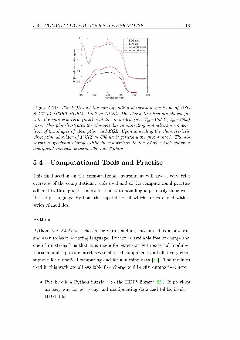
5.4. COMPUTATIONAL TOOLS AND PRACTISE 113
300 400 500 600 700 800Wavelength / nm
0
0.2
0.4
0.6
0.8
1
EQ
E /
arb.
uni
ts, A
bsor
ptio
n
EQE nanEQE anAbsorption nanAbsorption an
Figure 5.11: The EQE and the corresponding absorption spectrum of OSCS 421 p1 (P3HT:PCBM, 1:0.7 in DCB). The characteristics are shown forboth the non-annealed (nan) and the annealed (an, Tpt=150
C, tpt=300s)case. This plot illustrates the changes due to annealing and allows a compar-ison of the shapes of absorption and EQE. Upon annealing the characteristicabsorption shoulder of P3HT at 600nm is getting more pronounced. The ab-sorption spectrum changes little in comparison to the EQE, which shows asignicant increase between 320 and 630nm.
5.4 Computational Tools and Practise
This nal section on the computational environment will give a very brief
overview of the computational tools used and of the computational practise
adhered to throughout this work. The data handling is primarily done with
the script language Python, the capabilities of which are extended with a
series of modules.
Python
Python (ver 2.4.2) was chosen for data handling, because it is a powerful
and easy to learn scripting language. Python is available free of charge and
one of its strength is that it is made for extension with external modules.
These modules provide interfaces to all used components and oer very good
support for numerical computing and for analysing data [84]. The modules
used in this work are all available free charge and briey summarised here.
• Pytables is a Python interface to the HDF5 library [85]. It provides
an easy way for accessing and manipulating data and tables inside a
HDF5 le.
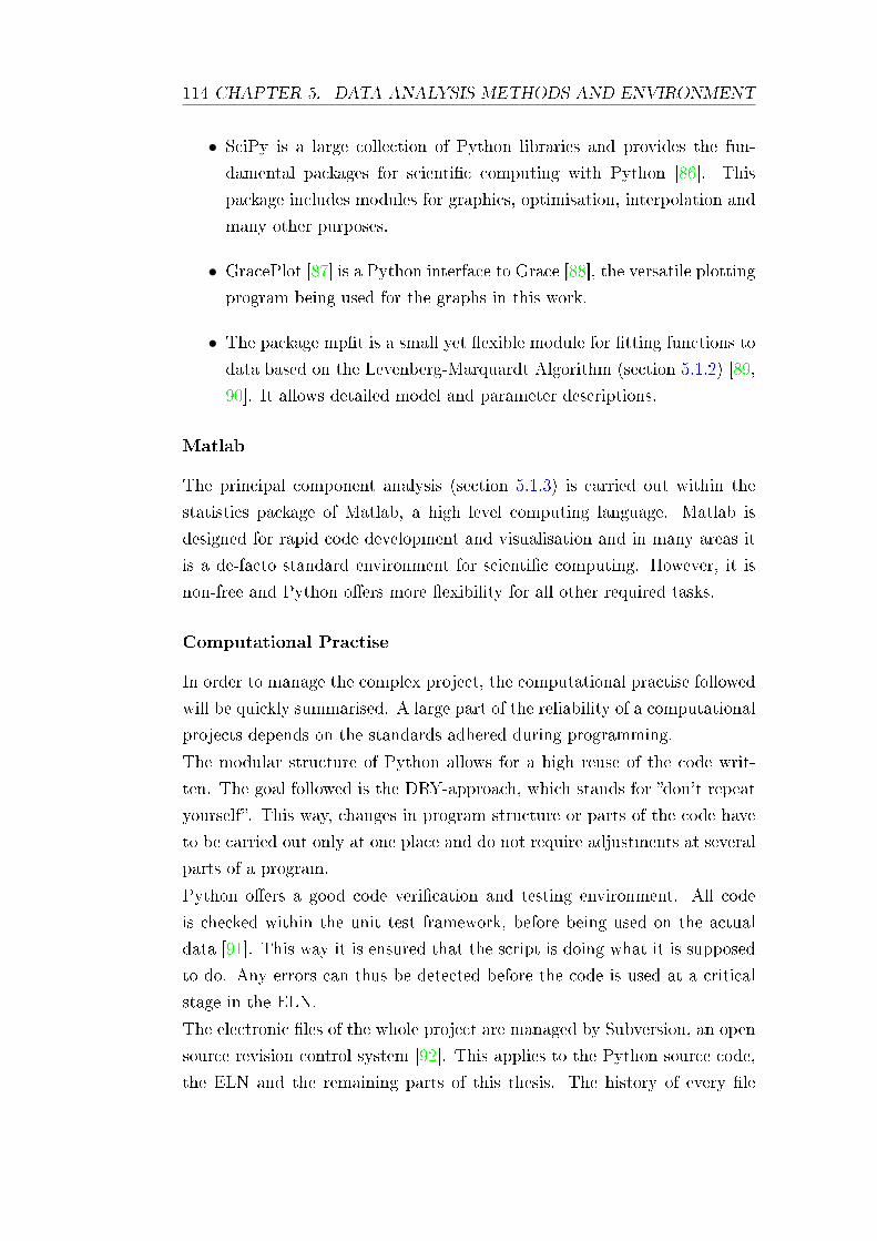
114 CHAPTER 5. DATA ANALYSIS METHODS AND ENVIRONMENT
• SciPy is a large collection of Python libraries and provides the fun-
damental packages for scientic computing with Python [86]. This
package includes modules for graphics, optimisation, interpolation and
many other purposes.
• GracePlot [87] is a Python interface to Grace [88], the versatile plotting
program being used for the graphs in this work.
• The package mpt is a small yet exible module for tting functions to
data based on the Levenberg-Marquardt Algorithm (section 5.1.2) [89,
90]. It allows detailed model and parameter descriptions.
Matlab
The principal component analysis (section 5.1.3) is carried out within the
statistics package of Matlab, a high level computing language. Matlab is
designed for rapid code development and visualisation and in many areas it
is a de-facto standard environment for scientic computing. However, it is
non-free and Python oers more exibility for all other required tasks.
Computational Practise
In order to manage the complex project, the computational practise followed
will be quickly summarised. A large part of the reliability of a computational
projects depends on the standards adhered during programming.
The modular structure of Python allows for a high reuse of the code writ-
ten. The goal followed is the DRY-approach, which stands for don't repeat
yourself. This way, changes in program structure or parts of the code have
to be carried out only at one place and do not require adjustments at several
parts of a program.
Python oers a good code verication and testing environment. All code
is checked within the unit test framework, before being used on the actual
data [91]. This way it is ensured that the script is doing what it is supposed
to do. Any errors can thus be detected before the code is used at a critical
stage in the ELN.
The electronic les of the whole project are managed by Subversion, an open
source revision control system [92]. This applies to the Python source code,
the ELN and the remaining parts of this thesis. The history of every le
5.5. SUMMARY 115
is documented and each le can be restored in a previous revision. While
modifying the HDF5 le, the script revision is recorded and modications
can be traced back to the program, which carried out the changes.
5.5 Summary
• In order to manage the large base of data, both with respect to quality
and size, the tools for an ecient data management were developed.
• An electronic laboratory notebook (ELN) unites data, which is coming
from two main sources: (1) from the production process, which is logged
through an user-friendly webinterface, and (2) from the automated OSC
characterisation, the data of which is made available in a standardised
format.
• The data in the ELN is hierarchically structured to allow an ecient
access. Data integrity is ensured by using the unit testing framework,
specifying read/write permissions to parts of the ELN and tracking any
change and associated scripts.
• The most common queries of the ELN have been automated, yet special
queries can be easily implemented.
• OSC properties are extracted from the measured data using cubic
splines and by tting model functions to the measured data using the
Levenberg-Marquardt Algorithm.
• Principal component analysis (PCA) has been chosen as multivariate
method to search for correlations between the production data and
OSC properties.
• Prior to analysis, the data is carefully checked and if necessary pruned.
The OSC preparation protocols are checked for missing or unreasonable
parameters. The measurement data is cleaned of OSCs, the observed
measurement characteristics of which can be explained by obvious de-
fects in the OSC.

116 CHAPTER 5. DATA ANALYSIS METHODS AND ENVIRONMENT
Chapter 6
Experiments and Analysis
In this chapter the inuence of the production process on the performance
of organic solar cells is investigated. First of all a large run of experiments
with a limited set of variations of the production parameters is described.
The resulting variations in OSC properties are examined both with respect
to the variations between the OSCs on one substrate and their variations
between dierent substrates. The range of observed OSC characteristics are
described with the example of three representative substrates covering the
range of obtained power conversion eciencies η. In order to determine the
causes of the observed spread in OSC properties, the data of the experiments
is searched for correlation between production parameters and measurement
results by means of principal component analysis (PCA). The correlations are
analysed for their physical origin and a model for optimising the production
process is proposed.
6.1 Inuence of the Production Process
During the production of the OSCs more than 40 parameters are recorded for
each substrate (section 3.2). The parameters were divided into three groups:
(1) parameters, which can be controlled well, e.g. the spin-coating speed used
for coating the substrates, and can be made identical for each substrate; (2)
the time intervals before and after a spin-coating step intrinsically vary from
substrate to substrate within one batch due to its sequential nature (see
gure 6.1); (3) there are parameters, which vary due to the human factor in
the production process, e.g. the manual control of the evaporation process,
or due to outside inuences, e.g. the temperature during spin-coating.
The variations of the parameters in groups (2) and (3) will be called unin-
117
118 CHAPTER 6. EXPERIMENTS AND ANALYSIS
.
.
.
.
.
.
.
.
.
.
.
.
.
.
.
Timestamp
Substrate 2:
Substrate 1:
14:15
14:15
Begin of Process
14:00
14:00 14:04
14:08
...
End of Process
∆ t1
∆ t1
= 4min
= 8min
∆ t2
∆ t2
= 11min
= 7min
Drying
(PEDOT:PSS)Cleaning Step
Last Substrate
Sequential Process Batch ProcessBatch Process
Spin−coating
(PEDOT:PSS)
Figure 6.1: The dierence in time intervals caused by the sequential natureof the spin-coating process. The example of the PEDOT:PSS spin-coatingillustrates the dierence in time intervals which arises from the sequence ofbatch processes and the spin-coating, i.e. a sequential process, where onlyone substrate at a time can be processed. A batch usually consists of eightsubstrates. The time intervals are obtained from the dierence in the times-tamps of the consecutive process steps in the electronic laboratory notebook(ELN).
tentional parameter variations in this chapter with the following reasoning:
they all vary and their variations are not or only very dicult to control.
The work is conducted with other researchers in the laboratory leading to
certain variations in the production process, e.g. when the evaporation cham-
ber is only available at a certain time. These variations due to the human
factor in the production and outside inuences like the temperature during
spin-coating introduce scatter in the production parameters. Thus there is
a minimal set of parameters, which unintentionally varies between every
OSC made in our laboratory. Unintentionally does not imply that these
variations are not useful. Quite the contrary, because this scatter leads to
variations in the OSC properties, which will be used in section 6.2 to analyse
the inuence of the involved production parameters.
Summarising, there exists a smallest set of parameters, which unintention-
ally varies between every made OSC. Prior to any intentional variation of
parameters in the production process, it essential to investigate the varia-
tions, which can be caused by this minimal set of such unintentional pa-
rameter variations. Without this knowledge it is at a later stage dicult
to assess, whether the variations observed in OSC properties are caused by
the unintentional variations or due to the intentional variation of additional
parameters. The question is: How much do the OSC properties vary due
to the unintentional variations? Thus during this run of experiments, all
parameters, which could be kept the same, were intentionally kept xed, and
a standardised production pattern was followed.
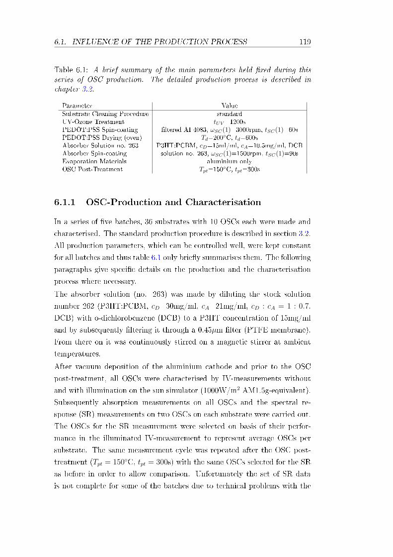
6.1. INFLUENCE OF THE PRODUCTION PROCESS 119
Table 6.1: A brief summary of the main parameters held xed during thisseries of OSC production. The detailed production process is described inchapter 3.2.
Parameter ValueSubstrate Cleaning Procedure standardUV-Ozone Treatment tUV =1200sPEDOT:PSS Spin-coating ltered AI 4083, ωSC(1)=3000rpm, tSC(1)=60sPEDOT:PSS Drying (oven) Td=200
C, td=600sAbsorber Solution no. 263 P3HT:PCBM, cD=15ml/ml, cA=10.5mg/ml, DCBAbsorber Spin-coating solution no. 263, ωSC(1)=1500rpm, tSC(1)=90sEvaporation Materials aluminium onlyOSC Post-Treatment Tpt=150
C, tpt=300s
6.1.1 OSC-Production and Characterisation
In a series of ve batches, 36 substrates with 10 OSCs each were made and
characterised. The standard production procedure is described in section 3.2.
All production parameters, which can be controlled well, were kept constant
for all batches and thus table 6.1 only briey summarises them. The following
paragraphs give specic details on the production and the characterisation
process where necessary.
The absorber solution (no. 263) was made by diluting the stock solution
number 262 (P3HT:PCBM, cD=30mg/ml, cA=21mg/ml, cD : cA = 1 : 0.7,
DCB) with o-dichlorobenzene (DCB) to a P3HT concentration of 15mg/ml
and by subsequently ltering it through a 0.45µm lter (PTFE membrane).
From there on it was continuously stirred on a magnetic stirrer at ambient
temperatures.
After vacuum deposition of the aluminium cathode and prior to the OSC
post-treatment, all OSCs were characterised by IV-measurements without
and with illumination on the sun simulator (1000W/m2 AM1.5g-equivalent).
Subsequently absorption measurements on all OSCs and the spectral re-
sponse (SR) measurements on two OSCs on each substrate were carried out.
The OSCs for the SR measurement were selected on basis of their perfor-
mance in the illuminated IV-measurement to represent average OSCs per
substrate. The same measurement cycle was repeated after the OSC post-
treatment (Tpt = 150C, tpt = 300s) with the same OSCs selected for the SR
as before in order to allow comparison. Unfortunately the set of SR data
is not complete for some of the batches due to technical problems with the
120 CHAPTER 6. EXPERIMENTS AND ANALYSIS
setup. Hence it is only used to supplement the conclusions.
Of the more than 40 recorded production parameters, it was found that 15
parameters varied during the production. These variations are called un-
intentional variations due to reasons described in 6.1 and all had not been
investigated systematically before. The following list explains all 15 produc-
tion parameters, with the variables and the short names used in the tables
with the PCA results (section 6.2). For ease of notation, the time intervals
before and after the spin-coating processes are labelled ∆t1 to ∆t4. For the
same reason, the layer index i for the evaporation is dropped, because there
is only the aluminium cathode layer:
• ∆t1=∆t[UV→PEDOT-SC]: The time interval between the UV-Ozone
treatment and the spin-coating (SC) of PEDOT:PSS in the cleanroom.
• ∆t2=∆t[PEDOT-SC→Oven]: The time interval between PEDOT:PSS
spin-coating and putting the substrates into an oven for PEDOT:PSS
drying.
• OP=Order of PEDOT-SC: In the attempt to keep the time interval be-
tween the UV-Ozone treatment and the PEDOT-SC short, the batch of
eight substrates was split into 2×4 substrates for cleaning and PEDOT-SC. Each group was prepared consecutively with a delay of approxi-
mately 20min (see gure 6.2).
• td(P )=Duration of PEDOT Drying: The duration of transferring the
substrates with the fresh PEDOT:PSS layer into the glovebox. During
this time the substrates are kept under vacuum in the airlock of a
glovebox.
• ∆t3=∆t[Airlock→Absorber-SC]: The time interval between taking the
substrates out of the airlock into the glovebox and spin-coating the
absorber layer.
• TSC=Temperature during Absorber-SC: The temperature inside the
glovebox during spin-coating the absorber layer.
• tsol=Age of Absorber-Solution: The time since the preparation of the
absorber solution no. 263.
6.1. INFLUENCE OF THE PRODUCTION PROCESS 121
• ∆t4=∆t[Absorber-SC→Vacuum]: The time interval between spin-coating
the absorber layer and putting the substrates into vacuum for drying.
• td(abs)=Duration of Absorber Drying: The duration of drying the ab-
sorber layer under vacuum prior to the evaporation step.
• tevac=Duration of Evaporation Vacuum: The period the substrates
spent in the high vacuum (<10−5mbar) of the evaporation chamber
before the Al-cathode is deposited.
• pbase=Evaporation Base Pressure: The base pressure in the evaporation
chamber for the deposition of the aluminium cathode.
• pevap=Evaporation Pressure: The average pressure during the deposi-
tion of the Al-cathode.
• ∆d5nm
∆t=Aluminium Rate <5nm: The evaporation rate of the rst 5nm
aluminium on the absorber layer, i.e. when the hot metal atoms get in
direct contact with the absorber layer.
• devap=Al-Layer Thickness: The nal layer thickness of the Al-cathode.
• tevap=Duration of Evaporation: The time the deposition of the Al-layer
took.
These variations constitute the least number of parameters varying during
OSC production and their range of variations is shown in table 6.2. Due
to a temporary limitation of being able to evaporate only four substrates
at a time, the rst two batches were split into two sequential evaporation
processes. The second evaporation process of batch 2 (4 substrates) was
excluded from the analysis, because its production diered from the above
described procedure in more than the selected parameters, leaving batch 2
with only four substrates. For the same reason, the complete batch 4 (8
substrates) had to be exempt from the analysis. Thus ve batches lead to a
total number of 36 substrates.
The parameter OP , i.e. the order of spin-coating of PEDOT:PSS, was in-
cluded in the analysis, because a univariate visualisation of the power conver-
sion eciency η versus the duration of PEDOT:PSS drying (td(P )) revealed
the only clear correlation in the whole data, which was obvious when looking
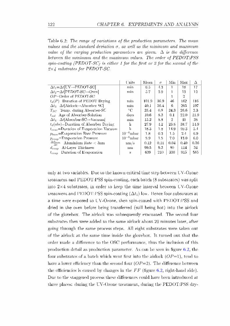
122 CHAPTER 6. EXPERIMENTS AND ANALYSIS
Table 6.2: The range of variations of the production parameters. The meanvalues and the standard deviation σ, as well as the minimum and maximumvalue of the varying production parameters are given. ∆ is the dierencebetween the minimum and the maximum values. The order of PEDOT:PSSspin-coating (PEDOT-SC) is either 1 for the rst or 2 for the second of the2×4 substrates for PEDOT-SC.
Units Mean σ Min Max ∆∆t1=∆t[UV→PEDOT-SC] min 6.5 4.3 1 18 17∆t2=∆t[PEDOT-SC→Oven] min 5.7 2.9 1 13 12OP=Order of PEDOT-SC 1 2td(P )=Duration of PEDOT Drying min 101.9 36.9 46 162 116∆t3=∆t[Airlock→Absorber-SC] min 40.1 56.4 6 203 197TSC=Temp. during Absorber-SC
C 25.4 0.8 24.3 26.6 2.3tsol=Age of Absorber-Solution days 10.6 8.3 0.1 22.0 21.9∆t4=∆t[Absorber-SC→Vacuum] min 15.2 8.8 2 40 38td(abs)=Duration of Absorber Drying h 27.9 4.2 23.8 38.7 14.9tevac=Duration of Evaporation Vacuum h 18.3 1.8 14.9 20.3 5.4pbase=Evaporation Base Pressure 10−6mbar 1.8 0.3 1.5 2.4 0.9pevap=Evaporation Pressure 10−6mbar 8.9 1.8 7.0 13.0 6.0∆d5nm
∆t =Aluminium Rate < 5nm nm/s 0.12 0.11 0.04 0.40 0.36devap=Al-Layer Thickness nm 99.5 9.3 80 114 34tevap=Duration of Evaporation s 639 210 330 915 585
only at two variables. Due to the known critical time step between UV-Ozone
treatment and PEDOT:PSS spin-coating, each batch (8 substrates) was split
into 2×4 substrates, in order to keep the time interval between UV-Ozone
treatment and PEDOT:PSS spin-coating (∆t1) low. Hence four substrates at
a time were exposed to UV-Ozone, then spin-coated with PEDOT:PSS and
dried in the oven before being transferred (still being hot) into the airlock
of the glovebox. The airlock was subsequently evacuated. The second four
substrates then were added to the same airlock about 20 minutes later, after
going through the same process steps. All eight substrates were taken out
of the airlock at the same time inside the glovebox. It turned out that the
order made a dierence to the OSC performance, thus the inclusion of this
production detail as production parameter. As can be seen in gure 6.2, the
four substrates of a batch which went rst into the airlock (OP=1), tend to
have a lower eciency than the second four (OP=2). The dierence between
the eciencies is caused by changes in the FF (gure 6.2, right-hand side).
Due to the staggered process these dierences could have been introduced at
three places: during the UV-Ozone treatment, during the PEDOT:PSS dry-
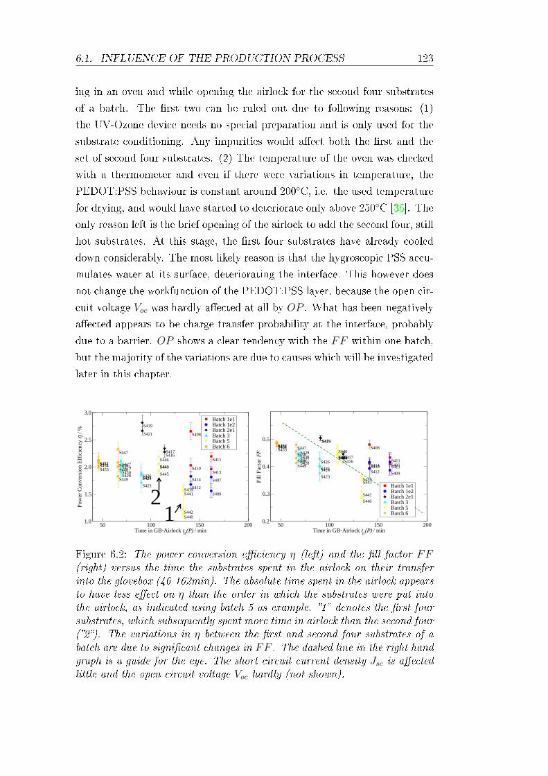
6.1. INFLUENCE OF THE PRODUCTION PROCESS 123
ing in an oven and while opening the airlock for the second four substrates
of a batch. The rst two can be ruled out due to following reasons: (1)
the UV-Ozone device needs no special preparation and is only used for the
substrate conditioning. Any impurities would aect both the rst and the
set of second four substrates. (2) The temperature of the oven was checked
with a thermometer and even if there were variations in temperature, the
PEDOT:PSS behaviour is constant around 200C, i.e. the used temperature
for drying, and would have started to deteriorate only above 250C [36]. The
only reason left is the brief opening of the airlock to add the second four, still
hot substrates. At this stage, the rst four substrates have already cooled
down considerably. The most likely reason is that the hygroscopic PSS accu-
mulates water at its surface, deteriorating the interface. This however does
not change the workfunction of the PEDOT:PSS layer, because the open cir-
cuit voltage Voc was hardly aected at all by OP . What has been negatively
aected appears to be charge transfer probability at the interface, probably
due to a barrier. OP shows a clear tendency with the FF within one batch,
but the majority of the variations are due to causes which will be investigated
later in this chapter.
S408
S410
S411
S413
S407
S409
S412
S414
S416S417
S419
S421
S423
S424S425S426
S427
S428
S429S430
S439
S440
S441
S442
S443S444
S445
S446
S447
S448
S449
S450S451S452S453S454
50 100 150 200Time in GB-Airlock td(P) / min
1.0
1.5
2.0
2.5
3.0
Pow
er C
onve
rsio
n E
ffic
ienc
y η
/ %
Batch 1e1Batch 1e2Batch 2e1Batch 3Batch 5Batch 6
12
Sat Nov 25 11:17:35 2006
S410S411S413
S408
S409S412
S414 S407
S417
S419S421
S416
S423
S424S425
S426S427S428
S429S430
S439
S440
S441
S442
S443S444S445S446
S447
S448S449
S450
S451S452S453S454
50 100 150 200Time in GB-Airlock td(P) / min
0.2
0.3
0.4
0.5
Fill
Fact
or F
F
Batch 1e1Batch 1e2Batch 2e1Batch 3Batch 5Batch 6
Sat Nov 25 11:17:55 2006
Figure 6.2: The power conversion eciency η (left) and the ll factor FF(right) versus the time the substrates spent in the airlock on their transferinto the glovebox (46-162min). The absolute time spent in the airlock appearsto have less eect on η than the order in which the substrates were put intothe airlock, as indicated using batch 5 as example. 1 denotes the rst foursubstrates, which subsequently spent more time in airlock than the second four(2). The variations in η between the rst and second four substrates of abatch are due to signicant changes in FF . The dashed line in the right handgraph is a guide for the eye. The short circuit current density Jsc is aectedlittle and the open circuit voltage Voc hardly (not shown).
124 CHAPTER 6. EXPERIMENTS AND ANALYSIS
Any inuence during the production process, which is dicult to quantify or
to incorporate into the data analysis was carefully considered and reduced as
much as possible. Each manual step was assigned to a specic experienced
experimenter such that the manual steps remained as consistent as possible.
All substrates were taken from the same ITO-glass batch and structured in
the same batch. During data cleaning all production parameters in questions
were resolved and no data of any substrate had to be excluded due to un-
known or obviously wrong entries. The data cleaning procedure is described
in section 5.3.1.
Summary
• 360 OSCs on 36 substrates were made in ve batches (4×8 and 1×4substrates). It has been found that the smallest set of variations during
production consists of 15 parameters out of the more than 40 recorded
ones and are subject to unintentional variations.
• For 14 of the 15 considered production parameters the unintentional
variations cannot be avoided due to the nature of the production pro-
cess or the human factor. The set of parameters consists e.g. of the
time intervals between production steps involving spin-coating, which
vary due the combination of batch and sequential processing, the tem-
perature during spin-coating of the absorber and the parameters of the
manually controlled evaporation of the aluminium cathode.
• The splitting of one batch (8 substrates) into 2×4 substrates for the
spin-coating of the PEDOT:PSS layer, additionally made an extra pa-
rameter (OP ) for their order necessary, because it aected the OSC
properties. The rst four substrates had a reduced FF , which is most
likely due to their exposure to ambient conditions after they had cooled
down. This parameter can and will be avoided in future by using a
second airlock for transferring the substrates into the glovebox after
spin-coating of the PEDOT:PSS layer.
• Variations in OP cannot explain all variations in η, because even when
removing the substrates, which are negatively aected by OP , the
range of variations in the power conversion η would only reduce from
1.1%↔2.8% to 1.7%↔2.8%.
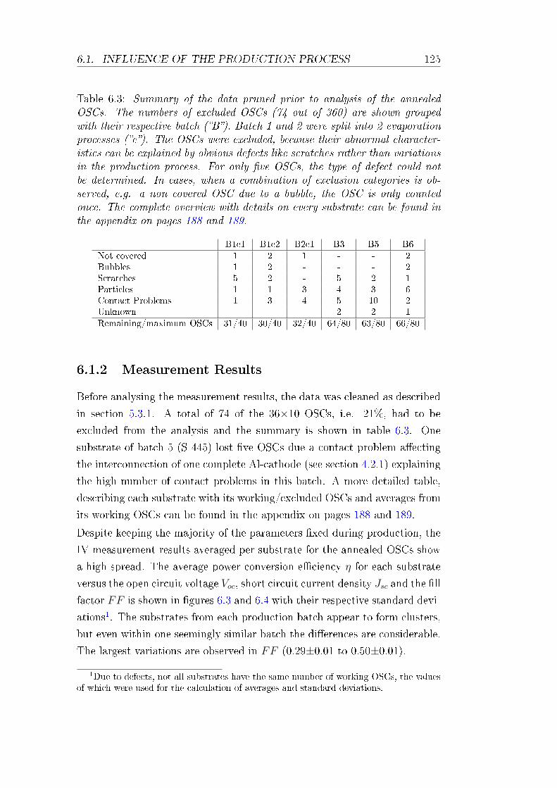
6.1. INFLUENCE OF THE PRODUCTION PROCESS 125
Table 6.3: Summary of the data pruned prior to analysis of the annealedOSCs. The numbers of excluded OSCs (74 out of 360) are shown groupedwith their respective batch (B). Batch 1 and 2 were split into 2 evaporationprocesses (e). The OSCs were excluded, because their abnormal character-istics can be explained by obvious defects like scratches rather than variationsin the production process. For only ve OSCs, the type of defect could notbe determined. In cases, when a combination of exclusion categories is ob-served, e.g. a non covered OSC due to a bubble, the OSC is only countedonce. The complete overview with details on every substrate can be found inthe appendix on pages 188 and 189.
B1e1 B1e2 B2e1 B3 B5 B6Not covered 1 2 1 - - 2Bubbles 1 2 - - - 2Scratches 5 2 - 5 2 1Particles 1 1 3 4 3 6Contact Problems 1 3 4 5 10 2Unknown - - - 2 2 1Remaining/maximum OSCs 31/40 30/40 32/40 64/80 63/80 66/80
6.1.2 Measurement Results
Before analysing the measurement results, the data was cleaned as described
in section 5.3.1. A total of 74 of the 36×10 OSCs, i.e. 21%, had to be
excluded from the analysis and the summary is shown in table 6.3. One
substrate of batch 5 (S 445) lost ve OSCs due a contact problem aecting
the interconnection of one complete Al-cathode (see section 4.2.1) explaining
the high number of contact problems in this batch. A more detailed table,
describing each substrate with its working/excluded OSCs and averages from
its working OSCs can be found in the appendix on pages 188 and 189.
Despite keeping the majority of the parameters xed during production, the
IV measurement results averaged per substrate for the annealed OSCs show
a high spread. The average power conversion eciency η for each substrate
versus the open circuit voltage Voc, short circuit current density Jsc and the ll
factor FF is shown in gures 6.3 and 6.4 with their respective standard devi-
ations1. The substrates from each production batch appear to form clusters,
but even within one seemingly similar batch the dierences are considerable.
The largest variations are observed in FF (0.29±0.01 to 0.50±0.01).
1Due to defects, not all substrates have the same number of working OSCs, the valuesof which were used for the calculation of averages and standard deviations.
126 CHAPTER 6. EXPERIMENTS AND ANALYSIS
Batches 1e1 and 1e2 were split at the evaporation process and form two
dierent clusters in the scatter plots. However, at this point it is not possible
to attribute the dierence solely to the evaporation process, because 1e1
and 1e2 diered in absorber drying times (td(abs)) as well. Furthermore,
from the scatter plots it is evident that there have to be more parameters
with an inuence on the shown OSC IV properties, than the parameters
of the evaporation process. Even substrates, which were evaporated in the
same evaporation process, exhibit a signicant spread. The dependence of
production parameters and OSC properties will be discussed in section 6.2
using a principal component analysis.
The histogram in gure 6.4 is based on the eciencies of all 286 OSCs used
in the analysis. The average η using all 286 OSCs is 2.0±0.4%. The long tailin the histogram indicates that apparently no fundamental upper limit of η
has been reached and there is much room for improvement. The range of
the obtained results is summarised in table 6.4. The physical aspects of the
dierences, both between substrates and between the OSCs on one substrate,
will be discussed in the following sections.
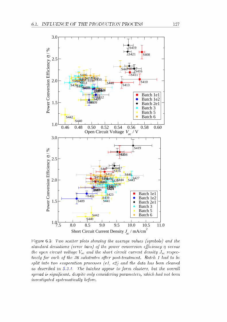
6.1. INFLUENCE OF THE PRODUCTION PROCESS 127
S408
S410
S411
S413
S407
S409
S412
S414
S416S417
S419
S421
S423
S424S425S426
S427
S428
S429S430
S439
S440
S441
S442
S443 S444
S445
S446
S447
S448
S449
S450S451S452S453S454
0.46 0.48 0.50 0.52 0.54 0.56 0.58 0.60Open Circuit Voltage Voc / V
1.0
1.5
2.0
2.5
3.0
Pow
er C
onve
rsio
n E
ffic
ienc
y η
/ %
Batch 1e1Batch 1e2Batch 2e1Batch 3Batch 5Batch 6
Sat Nov 25 11:17:00 2006
S408
S410
S411
S413
S407
S409
S412
S414
S416S417
S419
S421
S423
S424S425S426
S427
S428
S429S430
S439
S440
S441
S442
S443S444
S445
S446
S447
S448
S449
S450S451S452S453
S454
7.5 8.0 8.5 9.0 9.5 10.0 10.5 11.0
Short Circuit Current Density Jsc / mA/cm2
1.0
1.5
2.0
2.5
3.0
Pow
er C
onve
rsio
n E
ffic
ienc
y η
/ %
Batch 1e1Batch 1e2Batch 2e1Batch 3Batch 5Batch 6
Sat Nov 25 11:16:31 2006
Figure 6.3: Two scatter plots showing the average values (symbols) and thestandard deviations (error bars) of the power conversion eciency η versusthe open circuit voltage Voc and the short circuit current density Jsc respec-tively for each of the 36 substrates after post-treatment. Batch 1 had to besplit into two evaporation processes (e1, e2) and the data has been cleanedas described in 5.3.1. The batches appear to form clusters, but the overallspread is signicant, despite only considering parameters, which had not beeninvestigated systematically before.
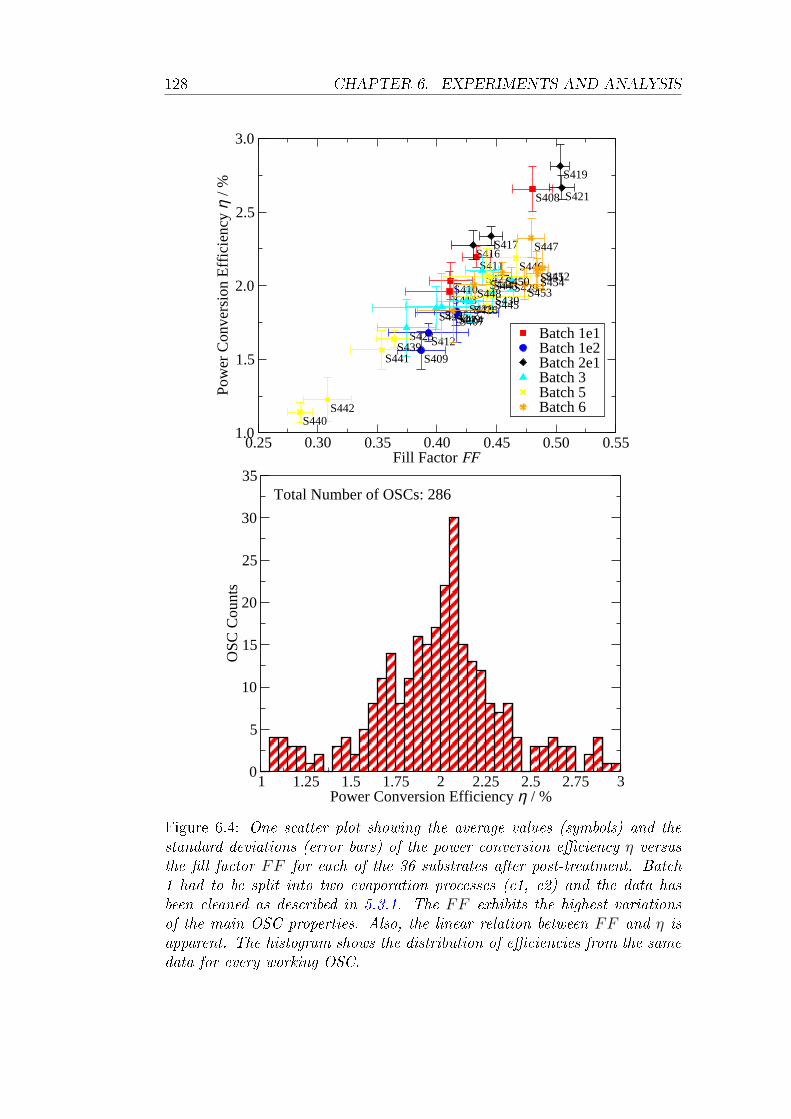
128 CHAPTER 6. EXPERIMENTS AND ANALYSIS
S408
S410
S411
S413
S407
S409
S412
S414
S416S417
S419
S421
S423
S424S425 S426
S427
S428
S429S430
S439
S440
S441
S442
S443S444
S445
S446
S447
S448
S449
S450 S451S452S453
S454
0.25 0.30 0.35 0.40 0.45 0.50 0.55Fill Factor FF
1.0
1.5
2.0
2.5
3.0
Pow
er C
onve
rsio
n E
ffic
ienc
y η
/ %
Batch 1e1Batch 1e2Batch 2e1Batch 3Batch 5Batch 6
Sat Nov 25 11:15:56 2006
1 1.25 1.5 1.75 2 2.25 2.5 2.75 3Power Conversion Efficiency η / %
0
5
10
15
20
25
30
35
OSC
Cou
nts
Total Number of OSCs: 286
Sat Nov 25 11:15:27 2006
Figure 6.4: One scatter plot showing the average values (symbols) and thestandard deviations (error bars) of the power conversion eciency η versusthe ll factor FF for each of the 36 substrates after post-treatment. Batch1 had to be split into two evaporation processes (e1, e2) and the data hasbeen cleaned as described in 5.3.1. The FF exhibits the highest variationsof the main OSC properties. Also, the linear relation between FF and η isapparent. The histogram shows the distribution of eciencies from the samedata for every working OSC.
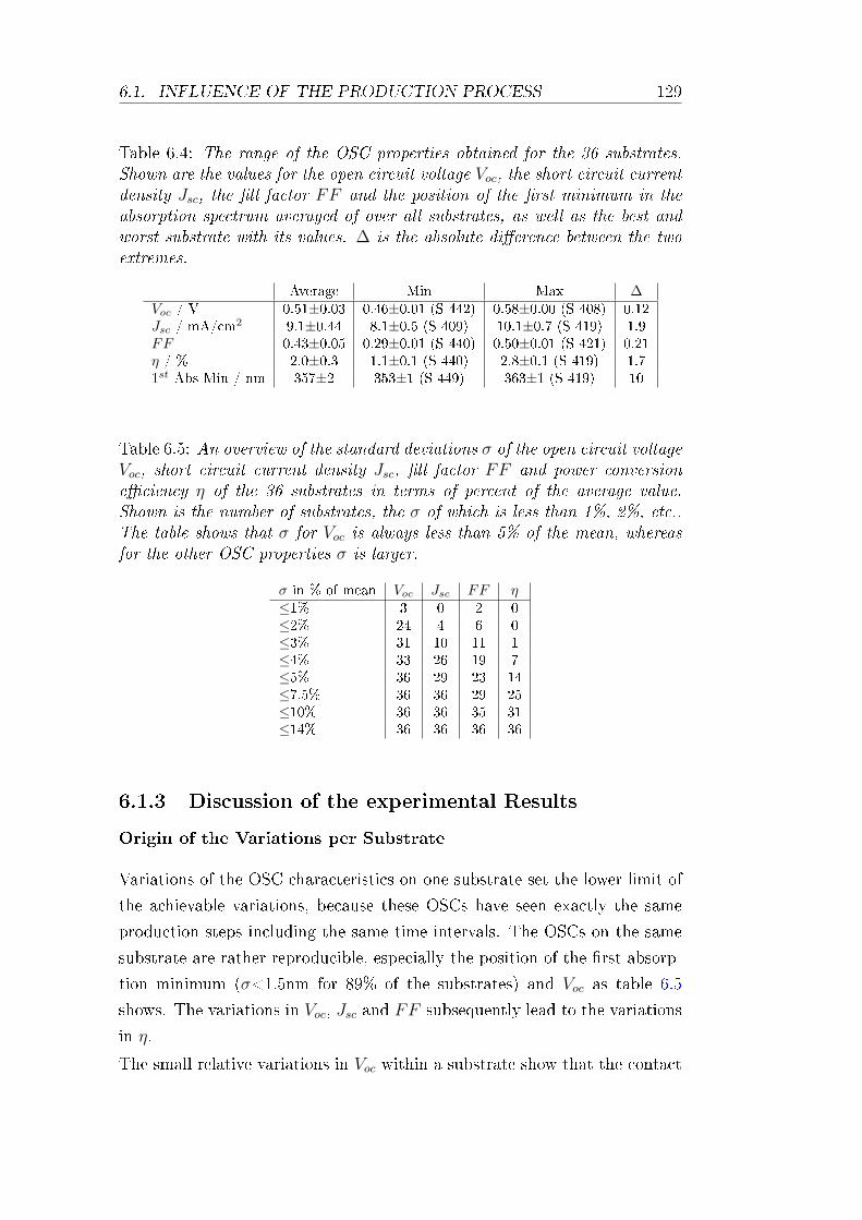
6.1. INFLUENCE OF THE PRODUCTION PROCESS 129
Table 6.4: The range of the OSC properties obtained for the 36 substrates.Shown are the values for the open circuit voltage Voc, the short circuit currentdensity Jsc, the ll factor FF and the position of the rst minimum in theabsorption spectrum averaged of over all substrates, as well as the best andworst substrate with its values. ∆ is the absolute dierence between the twoextremes.
Average Min Max ∆Voc / V 0.51±0.03 0.46±0.01 (S 442) 0.58±0.00 (S 408) 0.12Jsc / mA/cm
2 9.1±0.44 8.1±0.5 (S 409) 10.1±0.7 (S 419) 1.9FF 0.43±0.05 0.29±0.01 (S 440) 0.50±0.01 (S 421) 0.21η / % 2.0±0.3 1.1±0.1 (S 440) 2.8±0.1 (S 419) 1.71st Abs Min / nm 357±2 353±1 (S 449) 363±1 (S 419) 10
Table 6.5: An overview of the standard deviations σ of the open circuit voltageVoc, short circuit current density Jsc, ll factor FF and power conversioneciency η of the 36 substrates in terms of percent of the average value.Shown is the number of substrates, the σ of which is less than 1%, 2%, etc..The table shows that σ for Voc is always less than 5% of the mean, whereasfor the other OSC properties σ is larger.
σ in % of mean Voc Jsc FF η≤1% 3 0 2 0≤2% 24 4 6 0≤3% 31 10 11 1≤4% 33 26 19 7≤5% 36 29 23 14≤7.5% 36 36 29 25≤10% 36 36 35 31≤14% 36 36 36 36
6.1.3 Discussion of the experimental Results
Origin of the Variations per Substrate
Variations of the OSC characteristics on one substrate set the lower limit of
the achievable variations, because these OSCs have seen exactly the same
production steps including the same time intervals. The OSCs on the same
substrate are rather reproducible, especially the position of the rst absorp-
tion minimum (σ<1.5nm for 89% of the substrates) and Voc as table 6.5
shows. The variations in Voc, Jsc and FF subsequently lead to the variations
in η.
The small relative variations in Voc within a substrate show that the contact
130 CHAPTER 6. EXPERIMENTS AND ANALYSIS
properties do not change much per substrate. Thus the interfaces on either
side of the absorber layer, i.e. PEDOT:PSS anode and aluminium cathode,
can be considered rather uniform on the same substrate. Dierences in the
PEDOT:PSS workfunction across the substrates would immediately be re-
ected in the Voc, whereas changes in the workfunction of Al at the interface
can not be ruled out, because Voc is only very weakly dependent on the
metal workfunction [20]. Dierent contact barriers for charge injection and
extraction would only be seen in Voc in the extreme cases.
Variations in Jsc substrate-wise are slightly larger (see table 6.5). The short
circuit current density Jsc reacts very sensitively and in a non-linear way
to variations in the thickness of the absorber layer due to the optical inter-
ference pattern formed by reections o the aluminium cathode [65]. The
average standard deviation σ for the position of the rst absorber minimum,
a measure for the thickness of the absorber layer, per substrate is 1.0nm
(σmin=0.3nm, σmax= 2.2nm). However, a clear relation between absorption
minimum and Jsc within substrates is not observed. Other factors like mor-
phological dierences or particles in the photovoltaic active area might play
a more important role, but are dicult to quantify and give rise to several
uncertainties. The current density was computed under the assumption that
the photovoltaic active areas of all OSCs is 5.3mm2 and that area is given by
the overlap between the ITO bottom electrode and the Al top electrode. It
is however possible that during production the pattern of the two electrodes
does not match as shown in gure 4.8 on page 72. This can happen because
the ITO is structured on plates containing 36 substrates, which have to be
cut manually into 25×25mm2 pieces. Cutting the glass at an angle or not
along the right line shifts the ITO pattern with respect to the evaporated
aluminium pattern. The 25×25_10 layout (see gure 4.8) can only correct
for a certain amount of oset. However, this could only explain some of the
variations, because typically all OSCs on a substrate would be aected by
a reduction of the photovoltaic active area if the pattern of top and bottom
electrode does not align.
The FF exhibits the highest variations per substrate. By comparing the
variations in Jsc with those of FF no correlation is seen and the variations
in FF appear to be of dierent origin than the variations in Jsc. However,
even though Voc varies much less per substrates, the variations between FF
and Voc weakly correlate. This suggests that some variations have the same
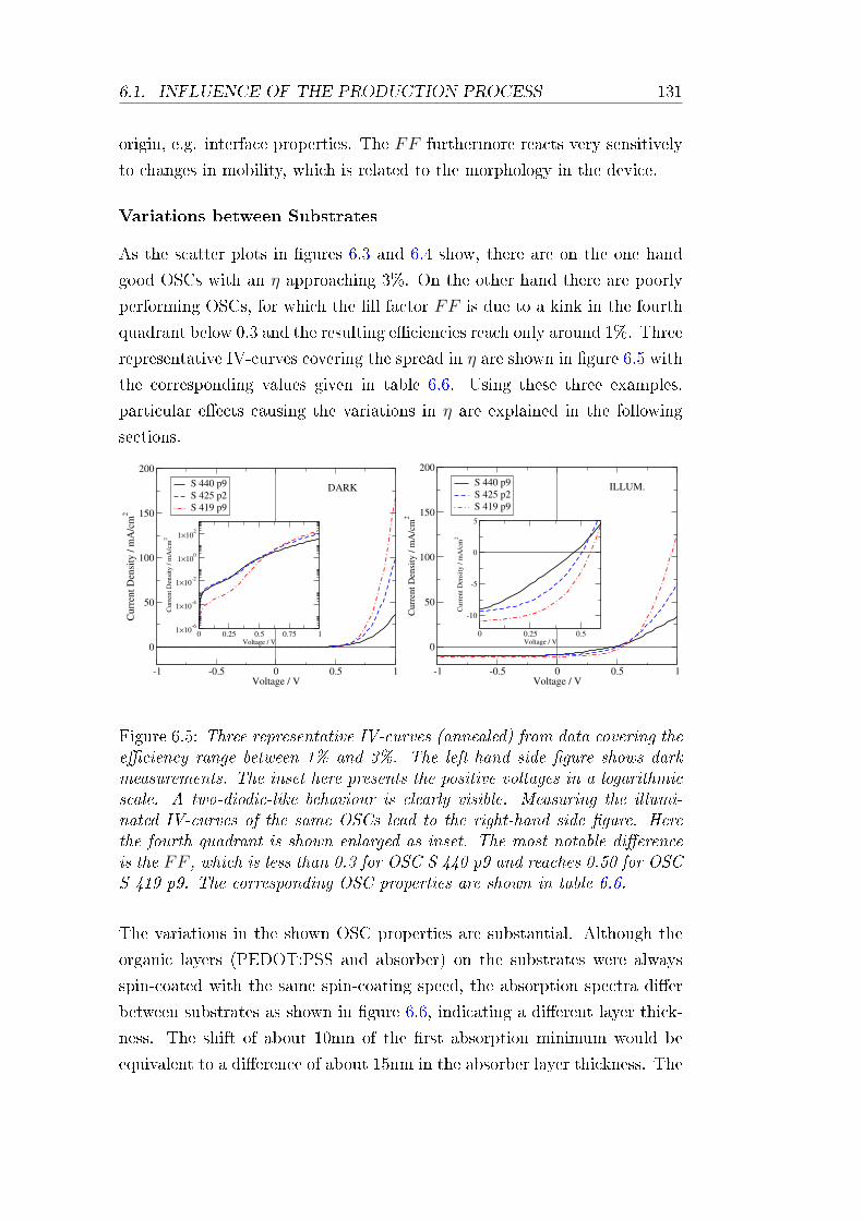
6.1. INFLUENCE OF THE PRODUCTION PROCESS 131
origin, e.g. interface properties. The FF furthermore reacts very sensitively
to changes in mobility, which is related to the morphology in the device.
Variations between Substrates
As the scatter plots in gures 6.3 and 6.4 show, there are on the one hand
good OSCs with an η approaching 3%. On the other hand there are poorly
performing OSCs, for which the ll factor FF is due to a kink in the fourth
quadrant below 0.3 and the resulting eciencies reach only around 1%. Three
representative IV-curves covering the spread in η are shown in gure 6.5 with
the corresponding values given in table 6.6. Using these three examples,
particular eects causing the variations in η are explained in the following
sections.
-1 -0.5 0 0.5 1Voltage / V
0
50
100
150
200
Cur
rent
Den
sity
/ m
A/c
m2
S 440 p9S 425 p2S 419 p9
0 0.25 0.5 0.75 1Voltage / V
1×10⁻⁶
1×10⁻⁴
1×10⁻²
1×100
1×10²
Cur
rent
Den
sity
/ m
A/c
m2
DARK
Tue Jul 11 16:26:32 2006-1 -0.5 0 0.5 1
Voltage / V
0
50
100
150
200
Cur
rent
Den
sity
/ m
A/c
m2
S 440 p9S 425 p2S 419 p9
0 0.25 0.5Voltage / V
-10
-5
0
5
Cur
rent
Den
sity
/ m
A/c
m2
ILLUM.
Tue Jul 11 16:28:50 2006
Figure 6.5: Three representative IV-curves (annealed) from data covering theeciency range between 1% and 3%. The left-hand side gure shows darkmeasurements. The inset here presents the positive voltages in a logarithmicscale. A two-diodic-like behaviour is clearly visible. Measuring the illumi-nated IV-curves of the same OSCs lead to the right-hand side gure. Herethe fourth quadrant is shown enlarged as inset. The most notable dierenceis the FF , which is less than 0.3 for OSC S 440 p9 and reaches 0.50 for OSCS 419 p9. The corresponding OSC properties are shown in table 6.6.
The variations in the shown OSC properties are substantial. Although the
organic layers (PEDOT:PSS and absorber) on the substrates were always
spin-coated with the same spin-coating speed, the absorption spectra dier
between substrates as shown in gure 6.6, indicating a dierent layer thick-
ness. The shift of about 10nm of the rst absorption minimum would be
equivalent to a dierence of about 15nm in the absorber layer thickness. The
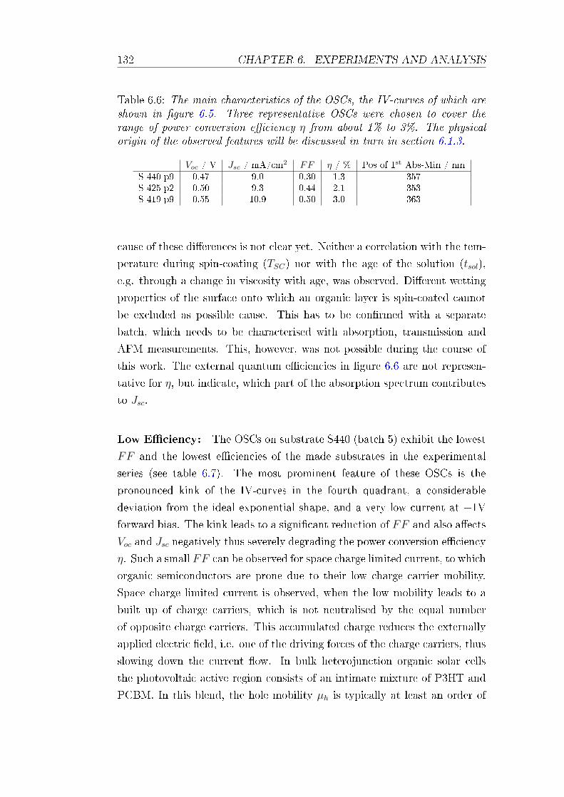
132 CHAPTER 6. EXPERIMENTS AND ANALYSIS
Table 6.6: The main characteristics of the OSCs, the IV-curves of which areshown in gure 6.5. Three representative OSCs were chosen to cover therange of power conversion eciency η from about 1% to 3%. The physicalorigin of the observed features will be discussed in turn in section 6.1.3.
Voc / V Jsc / mA/cm2 FF η / % Pos of 1st Abs-Min / nm
S 440 p9 0.47 9.0 0.30 1.3 357S 425 p2 0.50 9.3 0.44 2.1 353S 419 p9 0.55 10.9 0.50 3.0 363
cause of these dierences is not clear yet. Neither a correlation with the tem-
perature during spin-coating (TSC) nor with the age of the solution (tsol),
e.g. through a change in viscosity with age, was observed. Dierent wetting
properties of the surface onto which an organic layer is spin-coated cannot
be excluded as possible cause. This has to be conrmed with a separate
batch, which needs to be characterised with absorption, transmission and
AFM measurements. This, however, was not possible during the course of
this work. The external quantum eciencies in gure 6.6 are not represen-
tative for η, but indicate, which part of the absorption spectrum contributes
to Jsc.
Low Eciency: The OSCs on substrate S440 (batch 5) exhibit the lowest
FF and the lowest eciencies of the made substrates in the experimental
series (see table 6.7). The most prominent feature of these OSCs is the
pronounced kink of the IV-curves in the fourth quadrant, a considerable
deviation from the ideal exponential shape, and a very low current at +1V
forward bias. The kink leads to a signicant reduction of FF and also aects
Voc and Jsc negatively thus severely degrading the power conversion eciency
η. Such a small FF can be observed for space charge limited current, to which
organic semiconductors are prone due to their low charge carrier mobility.
Space charge limited current is observed, when the low mobility leads to a
built up of charge carriers, which is not neutralised by the equal number
of opposite charge carriers. This accumulated charge reduces the externally
applied electric eld, i.e. one of the driving forces of the charge carriers, thus
slowing down the current ow. In bulk heterojunction organic solar cells
the photovoltaic active region consists of an intimate mixture of P3HT and
PCBM. In this blend, the hole mobility µh is typically at least an order of
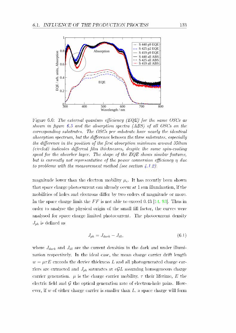
6.1. INFLUENCE OF THE PRODUCTION PROCESS 133
300 400 500 600 700 800Wavelength / nm
0
0.2
0.4
0.6
0.8
1
EQ
E /
arb.
uni
ts, A
bsor
ptio
n
S 440 p9 EQES 425 p2 EQES 419 p9 EQES 440 all ABSS 425 all ABSS 419 all ABS
EQE
Absorption
Figure 6.6: The external quantum eciency (EQE) for the same OSCs asshown in gure 6.5 and the absorption spectra (ABS) of all OSCs on thecorresponding substrates. The OSCs per substrate have nearly the identicalabsorption spectrum, but the dierence between the three substrates, especiallythe dierence in the position of the rst absorption minimum around 350nm(circled) indicates dierent lm thicknesses, despite the same spin-coatingspeed for the absorber layer. The shape of the EQE shows similar features,but is currently not representative of the power conversion eciency η dueto problems with the measurement method (see section 4.1.2).
magnitude lower than the electron mobility µe. It has recently been shown
that space charge photocurrent can already occur at 1 sun illumination, if the
mobilities of holes and electrons dier by two orders of magnitude or more.
In the space charge limit the FF is not able to exceed 0.43 [14, 93]. Thus in
order to analyse the physical origin of the small ll factor, the curves were
analysed for space charge limited photocurrent. The photocurrent density
Jph is dened as
Jph = Jdark − Jill, (6.1)
where Jdark and Jill are the current densities in the dark and under illumi-
nation respectively. In the ideal case, the mean charge carrier drift length
w = µτE exceeds the device thickness L and all photogenerated charge car-
riers are extracted and Jph saturates at eGL assuming homogeneous charge
carrier generation. µ is the charge carrier mobility, τ their lifetime, E the
electric eld and G the optical generation rate of electron-hole pairs. How-
ever, if w of either charge carrier is smaller than L, a space charge will form
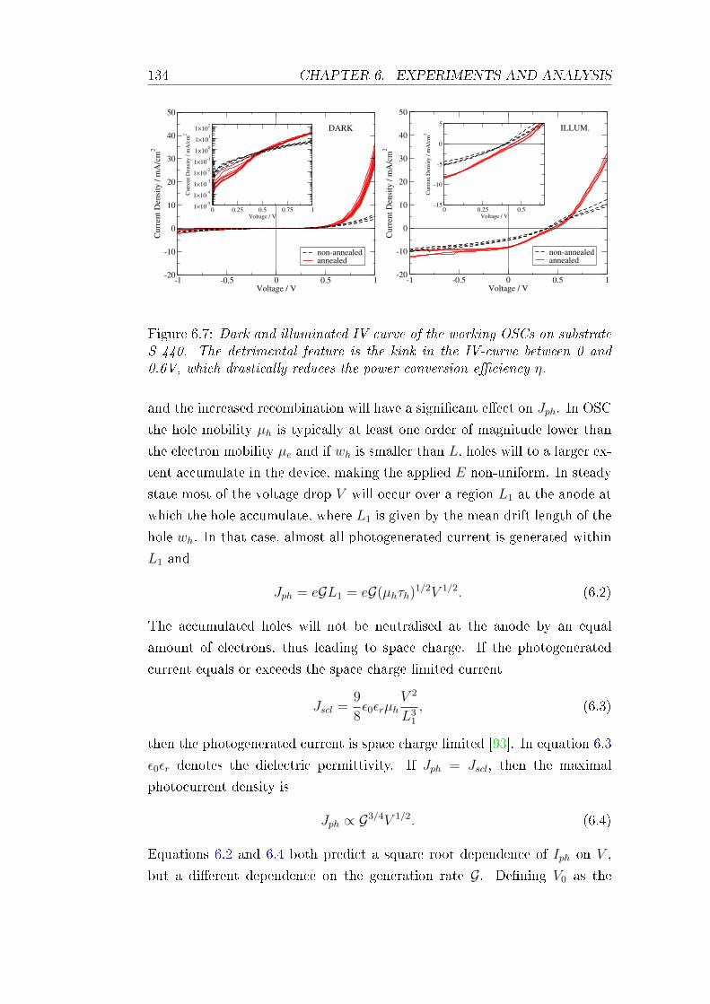
134 CHAPTER 6. EXPERIMENTS AND ANALYSIS
-1 -0.5 0 0.5 1Voltage / V
-20
-10
0
10
20
30
40
50
Cur
rent
Den
sity
/ m
A/c
m2
non-annealedannealed
0 0.25 0.5 0.75 1Voltage / V
1×10⁻⁵
1×10⁻⁴
1×10⁻³
1×10⁻²
1×10⁻¹
1×100
1×101
1×10²
Cur
rent
Den
sity
/ m
A/c
m2
DARK
Mon Jul 17 23:08:11 2006
-1 -0.5 0 0.5 1Voltage / V
-20
-10
0
10
20
30
40
50
Cur
rent
Den
sity
/ m
A/c
m2
non-annealedannealed
0 0.25 0.5Voltage / V
-15
-10
-5
0
5
Cur
rent
Den
sity
/ m
A/c
m2
ILLUM.
Mon Jul 17 23:09:42 2006
Figure 6.7: Dark and illuminated IV curve of the working OSCs on substrateS 440. The detrimental feature is the kink in the IV-curve between 0 and0.6V, which drastically reduces the power conversion eciency η.
and the increased recombination will have a signicant eect on Jph. In OSC
the hole mobility µh is typically at least one order of magnitude lower than
the electron mobility µe and if wh is smaller than L, holes will to a larger ex-
tent accumulate in the device, making the applied E non-uniform. In steady
state most of the voltage drop V will occur over a region L1 at the anode at
which the hole accumulate, where L1 is given by the mean drift length of the
hole wh. In that case, almost all photogenerated current is generated within
L1 and
Jph = eGL1 = eG(µhτh)1/2V 1/2. (6.2)
The accumulated holes will not be neutralised at the anode by an equal
amount of electrons, thus leading to space charge. If the photogenerated
current equals or exceeds the space charge limited current
Jscl =9
8ε0εrµh
V 2
L31
, (6.3)
then the photogenerated current is space charge limited [93]. In equation 6.3
ε0εr denotes the dielectric permittivity. If Jph = Jscl, then the maximal
photocurrent density is
Jph ∝ G3/4V 1/2. (6.4)
Equations 6.2 and 6.4 both predict a square root dependence of Iph on V ,
but a dierent dependence on the generation rate G. Dening V0 as the
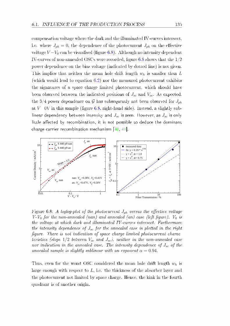
6.1. INFLUENCE OF THE PRODUCTION PROCESS 135
compensation voltage where the dark and the illuminated IV-curves intersect,
i.e. where Jph = 0, the dependence of the photocurrent Jph on the eective
voltage V −V0 can be visualised (gure 6.8). Although no intensity dependent
IV-curves of non-annealed OSCs were recorded, gure 6.8 shows that the 1/2
power dependence on the bias voltage (indicated by dotted line) is not given.
This implies that neither the mean hole drift length wh is smaller than L
(which would lead to equation 6.2) nor the measured photocurrent exhibits
the signatures of a space charge limited photocurrent, which should have
been observed between the indicated positions of Jsc and Voc. As expected,
the 3/4 power dependence on G has subsequently not been observed for Jph
at V=0V in this sample (gure 6.8, right-hand side). Instead, a slightly sub-
linear dependency between intensity and Jsc is seen. However, as Jsc is only
little aected by recombination, it is not possible to deduce the dominant
charge carrier recombination mechanism [40, 41].
0.01 0.1 1V - V
0 / V
0
1
10
Cur
rent
Den
sity
/ m
A/c
m2
Jph S 440 p9 nan
Jph S 440 p9 an
nan: Voc=0.38V, V0=0.41V
an: Voc=0.47V, V0=0.50V
Slope = 1/2
Voc an
Voc nan
Jsc an
Jsc nan
Sat Nov 25 11:23:47 20060.1 1 10 100
Filter Transmission / %
0.1
1
10
J ph =
J sc a
t V=
0V /
mA
/cm
2
measured datafit: y = 0.19 * x
0.94
y = xα, α = 1.0
y = xα, α= 0.75
Sat Nov 25 11:24:48 2006
Figure 6.8: A loglog-plot of the photocurrent Jph versus the eective voltageV-V0 for the non-annealed (nan) and annealed (an) case (left gure). V0 isthe voltage at which dark and illuminated IV-curves intersect. Furthermorethe intensity dependence of Jsc for the annealed case is plotted in the rightgure. There is not indication of space charge limited photocurrent charac-teristics (slope 1/2 between Voc and Jsc), neither in the non-annealed casenor indication in the annealed case. The intensity dependence of Jsc of theannealed sample is slightly sublinear with an exponent α = 0.94.
Thus, even for the worst OSC considered the mean hole drift length wh is
large enough with respect to L, i.e. the thickness of the absorber layer and
the photocurrent not limited by space charge. Hence, the kink in the fourth
quadrant is of another origin.
136 CHAPTER 6. EXPERIMENTS AND ANALYSIS
Table 6.7: The main OSC properties of substrate S 440. The table showsthe non-annealed and annealed averages for the number of working OSCs onthe substrate. ∆ gives the percentage change with respect to the non-annealedvalues.
S 440 non-annealed S 440 annealed ∆ / %No of working cells 6 8Voc / V 0.38±0.02 0.47±0.01 +24Jsc / mA/cm
2 4.8±0.3 8.4±0.3 +75FF 0.31±0.02 0.29±0.01 -6η / % 0.6±0.1 1.1±0.1 +83
In reference [14] the authors do not state the solvent of the absorber solution.
However, from the increase in photocurrent and absorption they observe, the
solvent was most likely a fast evaporating, i.e. low boiling point, solvent,
leading to disadvantageous morphology in the non-annealed state. Their
measured hole mobility was below 10−7cm2(Vs)−1, whereas the electron mo-
bility was three orders of magnitude higher. The absorber solution 263, with
which substrate S 440 was prepared, however uses DCB as solvent, which has
a high boiling point (180C). Thus the morphology in the non-annealed case
is already more advantageous and the hole mobility µh is already suciently
high as not to lead to space charge limited photocurrent.
The slope of Jph between the indicated Jsc and Voc is nearly 1 in the annealed
case, indicating that in this region Jph is approximately proportional to V . In
reverse bias, all photogenerated charge carriers are extracted and Jph as well
as J saturates, excluding a shunt resistance a possible cause. At forward bias
Jph has a linear relationship with V − V0 until the electrode start to inject
charges. Substrate S 440 belongs to the four substrates of batch 5, which were
spin-coated with PEDOT:PSS rst, i.e. OP=1. Figure 6.2 clearly shows a
correlation between OP and the FF . Substrates with OP=1 were exposed to
ambient conditions after they have cooled down from the PEDOT:PSS drying
temperature, which apparently has a detrimental eect on the FF . This
suggests that the PEDOT:PSS interface might have degraded. Subsequent
impedance spectroscopy measurements additionally indicate an barrier at the
Al-interface which aects charge extraction [94]. Simulations have indeed
shown that the kink in the IV-curve can be reproduced by lowering the
transfer probability of electrons into the cathode. Whereas at Jsc the built-
in potential is still large enough to drive the electrons across the Al interface,
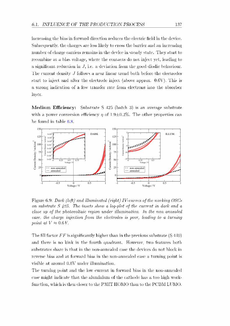
6.1. INFLUENCE OF THE PRODUCTION PROCESS 137
increasing the bias in forward direction reduces the electric eld in the device.
Subsequently, the charges are less likely to cross the barrier and an increasing
number of charge carriers remains in the device in steady state. They start to
recombine at a bias voltage, where the contacts do not inject yet, leading to
a signicant reduction in J , i.e. a deviation from the good diodic behaviour.
The current density J follows a near linear trend both before the electrodes
start to inject and after the electrode inject (above approx. 0.6V). This is
a strong indication of a low transfer rate from electrons into the absorber
layer.
Medium Eciency: Substrate S 425 (batch 3) is an average substrate
with a power conversion eciency η of 1.9±0.2%. The other properties canbe found in table 6.8.
-1 -0.5 0 0.5 1Voltage / V
0
25
50
75
100
125
150
Cur
rent
Den
sity
/ m
A/c
m2
non-annealedannealed
0 0.25 0.5 0.75 1Voltage / V
1×10⁻⁵
1×10⁻⁴
1×10⁻³
1×10⁻²
1×10⁻¹
1×100
1×101
1×10²
Cur
rent
Den
sity
/ m
A/c
m2
DARK
Mon Jul 17 23:06:33 2006
-1 -0.5 0 0.5 1Voltage / V
0
25
50
75
100
125
150
Cur
rent
Den
sity
/ m
A/c
m2
non-annealedannealed
0 0.25 0.5Voltage / V
-15
-10
-5
0
5
Cur
rent
Den
sity
/ m
A/c
m2
ILLUM.
Mon Jul 17 23:06:51 2006
Figure 6.9: Dark (left) and illuminated (right) IV-curves of the working OSCson substrate S 425. The insets show a log-plot of the current in dark and aclose-up of the photovoltaic region under illumination. In the non-annealedcase, the charge injection from the electrodes is poor, leading to a turningpoint at V ≈ 0.6V.
The ll factor FF is signicantly higher than in the previous substrate (S 440)
and there is no kink in the fourth quadrant. However, two features both
substrates share is that in the non-annealed case the devices do not block in
reverse bias and at forward bias in the non-annealed case a turning point is
visible at around 0.6V under illumination.
The turning point and the low current in forward bias in the non-annealed
case might indicate that the aluminium of the cathode has a too high work-
function, which is then closer to the P3HT HOMO than to the PCBM LUMO.
138 CHAPTER 6. EXPERIMENTS AND ANALYSIS
Table 6.8: The main OSC properties of substrate S 425. The table showsthe non-annealed and annealed averages for the number of working OSCs onthe substrate. ∆ gives the percentage change with respect to the non-annealedvalues.
S 425 non-annealed S 425 annealed ∆ / %No of working cells 8 9Voc / V 0.42±0.02 0.50±0.01 +19Jsc / mA/cm
2 6.6±0.5 9.1±0.4 +38FF 0.33±0.03 0.40±0.03 +21η / % 0.9±0.2 1.9±0.2 +111
Thus charge injection is severely inhibited in forward bias, but current ex-
traction from the device is only little aected. The turning point around 0.6V
disappears during annealing and the current density increased by nearly an
order of magnitude at 1V forward bias. The barrier, which inhibited charge
injection in the non-annealed case, is apparently reduced signicantly and
consequently, the electrodes can supply more current at the same bias volt-
age.
The opening of the diode in reverse bias might be due to small defects in
the absorber layer, which enable charge carriers to pass through. This also
implies that parts of the electrode are failing, because charges are injected.
If the workfunction of the aluminium in the non-annealed case is too high,
the current could originate from hole injection from the Al-cathode via one-
electron states in the band gap caused by these eects.
The physical origin of the turning point at about 0.6V and the opening of
the diode in reverse bias is subject to current discussions and investigated by
electrical device simulations.
High Eciency: The OSCs on substrate S 419 (batch 2e1) already show
in the non-annealed state a good diodic behaviour with no apparent opening
of the diode in reverse bias as shown in gure 6.10 (left). The OSC properties
for the non-annealed and annealed case are given in table 6.9.
Something, which has been observed throughout batch 2e1, but for no other
batch, is the decrease of the Vov upon annealing. For substrate S 419, the Voc
dropped from 0.65V to 0.56V, i.e. nearly 100mV. In darkness, the interfaces
start to inject earlier in the annealed than in the non-annealed case when
going to forward bias. This is also visible for the illuminated case. The
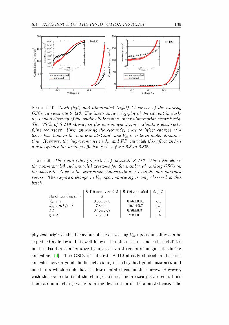
6.1. INFLUENCE OF THE PRODUCTION PROCESS 139
-1 -0.5 0 0.5 1Voltage / V
0
50
100
150
200C
urre
nt D
ensi
ty /
mA
/cm
2
non-annealedannealed
0 0.25 0.5 0.75 1Voltage / V
1×10⁻⁵
1×10⁻⁴
1×10⁻³
1×10⁻²
1×10⁻¹
1×100
1×101
1×10²
Cur
rent
Den
sity
/ m
A/c
m2
DARK
Mon Jul 17 23:03:00 2006
-1 -0.5 0 0.5 1Voltage / V
0
50
100
150
200
Cur
rent
Den
sity
/ m
A/c
m2
non-annealedannealed
0 0.25 0.5Voltage / V
-15
-10
-5
0
5
Cur
rent
Den
sity
/ m
A/c
m2
ILLUM.
Mon Jul 17 23:06:04 2006
Figure 6.10: Dark (left) and illuminated (right) IV-curves of the workingOSCs on substrate S 419. The insets show a log-plot of the current in dark-ness and a close-up of the photovoltaic region under illumination respectively.The OSCs of S 419 already in the non-annealed state exhibits a good recti-fying behaviour. Upon annealing the electrodes start to inject charges at alower bias than in the non-annealed state and Voc is reduced under illumina-tion. However, the improvements in Jsc and FF outweigh this eect and asa consequence the average eciency rises from 2.3 to 2.8%.
Table 6.9: The main OSC properties of substrate S 419. The table showsthe non-annealed and annealed averages for the number of working OSCs onthe substrate. ∆ gives the percentage change with respect to the non-annealedvalues. The negative change in Voc upon annealing is only observed in thisbatch.
S 419 non-annealed S 419 annealed ∆ / %No of working cells 5 6Voc / V 0.65±0.00 0.56±0.01 -14Jsc / mA/cm
2 7.8±0.4 10.1±0.7 +29FF 0.46±0.02 0.50±0.01 +9η / % 2.3±0.1 2.8±0.1 +22
physical origin of this behaviour of the decreasing Vov upon annealing can be
explained as follows. It is well known that the electron and hole mobilities
in the absorber can improve by up to several orders of magnitude during
annealing [14]. The OSCs of substrate S 419 already showed in the non-
annealed case a good diodic behaviour, i.e. they had good interfaces and
no shunts which would have a detrimental eect on the curves. However,
with the low mobility of the charge carriers, under steady state conditions
there are more charge carriers in the device than in the annealed case. The
140 CHAPTER 6. EXPERIMENTS AND ANALYSIS
increased charge carrier density leads to an increased splitting of the QFL
(see equation 2.9) and thus a higher Voc is possible in the non-annealed case.
After annealing, the mobility of the charge carriers is increased and they do
not remain as long in the device as before, thus reducing the charge carrier
density and the splitting of the QFL. Voc is reduced, but the overall eciency
still increases, due to an improvement in Jsc and FF .
It is yet not understood why the substrates from this batch had this be-
haviour. Their absorber layer dried very long in the vacuum and in the
evaporation chamber, but these time intervals for batch 6 were longer. Only
the duration of evaporation is the shortest (315s) for batch 2e1. Still, the
duration of evaporation for batch 1e1 was only 15s longer and did not show
a drop in Voc upon annealing. In literature both behaviours can be found,
e.g. for dropping Voc upon annealing see reference [95] and for an increasing
Voc see reference [96], but neither comment on the change in Voc.
OSCs, which do not exhibit a good diodic behaviour in the non-annealed
case, do not show this eect, because shunts have an adverse eect on the
Voc which dominates. During post-treatment, these shunts are burnt out and
the Voc rises, i.e. this improvement outweighs the decrease in Voc due to an
increased charge carrier mobility.
6.1.4 Conclusions
• Despite the variations of the least number of production parameters
possible, it was found that the spread in the OSC properties is much
larger than the expected. For a reproducible production process vari-
ations in the power conversion eciency η of ±10% around the mean,
i.e. here (2.0±0.2)%, would be reasonable, but a spread of nearly ±50%around the mean was obtained (1.1%≤ η ≤2.8%). The largest varia-
tions are seen in the ll factor FF , which varies between 0.29 and 0.50.
The variations in Voc and Jsc were 0.46-0.58V and 8.1-10.1mA/cm2
respectively.
• FF is the key parameter governing the power conversion eciency η in
the experiments. Improving the FF from the obtained values to 0.6,
which is often reported in literature, will lead to an η>3.5%.
• The production parameters, which unintentionally varied in this set
of experiments, are hardly mentioned in literature, but introduced a
6.1. INFLUENCE OF THE PRODUCTION PROCESS 141
signicant spread in the measured OSC properties. This puts the re-
sults published in literature into a new light, if only the results of a
few OSCs without shown signicance are presented, and stresses that
a high number of experiments has to be conducted to verify the eects
observed in OSCs.
• Voc appears to be the most reproducible property of the OSCs on the
same substrate.
• The variations in Jsc per substrate are likely due to a combination
of morphological eects and particles in the absorber layer, although
variations resulting from errors in the active area cannot be excluded.
• The FF of the OSCs on the same substrate varies most. It is aected by
both the transfer rates at the contacts and the charge carrier transport
through the blend of P3HT and PCBM, which is highly dependent on
the morphology, i.e. the way P3HT and PCBM arrange during drying
and annealing of the absorber. This is consistent with the fact that the
morphology might change within a substrate.
• The lowest observed FF cannot be explained by space charge limited
current which is often observed in organic semiconductors. Rather,
limitations from the interfaces are thought to cause the found char-
acteristics, with contributions from both aluminium and PEDOT:PSS
interface. Subsequent impedance spectroscopy measurements seem to
conrm this assumption.
• Jsc scales slightly sublinear with light intensity even for the worst OSCs.
Thus recombination only plays a minor role at short circuit conditions
and no conclusions can be drawn on the dominant recombination mech-
anism.
• Voc increases upon annealing on average by 70mV. Then the behaviour
of non-annealed IV-curves is dominated by shunts, which are reduced
during annealing. If the non-annealed IV-curves show a good diodic
behaviour Voc can fall up to nearly 100mV due to the increase of the
mobility and the subsequently reduced splitting of the QFLs in the
device. In both cases Voc ends up in the same region for the annealed
devices.
142 CHAPTER 6. EXPERIMENTS AND ANALYSIS
6.2 Principal Component Analysis
The main observed phenomena in the measured OSCs and their underlying
physics presented in section 6.1 can qualitatively be explained, but it is di-
cult to identify a dependency between specic production steps and the OSC
properties. All substrates dier in not only one production parameter at a
time, but several. In order to analyse the correlations between the produc-
tion parameters and the OSC properties, the principal component analysis
(PCA, see section 5.1.3) is used. The aim is to nd out where the observed
variations in the OSC properties come from in the production process, and
to systematically determine the correlation between the OSC properties and
the production parameters.
During production, the majority of the production parameters could be kept
constant and only a limited set was subject to unintentional variations (see
section 6.1.1). As the data is not commensurate, i.e. diers in scale and
variances, the correlation matrix R (see section 5.1.3) is used for all PCAs
in this section and only the measurement data from annealed OSCs is used.
Through a diagonalisation of R one obtains the corresponding eigenvectors
eα and eigenvalues λα. The eigenvectors are called principal component
vectors (PCV) and form the basis of the new coordinate system, into which
the original data is transformed. The new variables describing the data
are called principal components (PCs) and are linear combinations of the
original variables. The PCs are sorted by descending eigenvalue λα, which is
a measure of the information content of a PC.
When interpreting the results of a PCA, the high dimensionality of the space
must be kept in mind. Considering the largest contributions of a PCV in
order to explain a trend can only be considered to be a 0th order approxi-
mation. To move parallel to one PC, all components have to be considered
simultaneously according to their weight.
Assuming that all important production parameters were included in the
analysis, it should be possible to trace the origin of the variations in OSC
properties back to the unintentional variations of a particular production
process (see section 6.1). Understanding these eects will eventually allow
an adjustment of those production parameters, such that they have a positive
eect on OSC performance. Furthermore, if additional intentional variations
of production parameters are introduced, it should be possible to separate
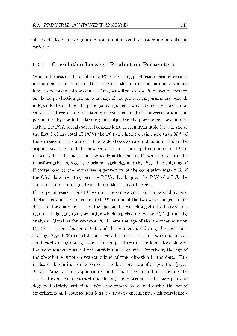
6.2. PRINCIPAL COMPONENT ANALYSIS 143
observed eects into originating from unintentional variations and intentional
variations.
6.2.1 Correlation between Production Parameters
When interpreting the results of a PCA including production parameters and
measurement result, correlations between the production parameters alone
have to be taken into account. Thus, as a rst step a PCA was performed
on the 15 production parameters only. If the production parameters were all
independent variables, the principal components would be nearly the original
variables. However, despite trying to avoid correlations between production
parameters by carefully planning and adjusting the parameters for compen-
sation, the PCA reveals several correlations, as seen from table 6.10. It shows
the rst 6 of the total 15 PCVs the PCs of which contain more than 89% of
the variance in the data set. The table shows as row and column header the
original variables and the new variables, i.e. principal components (PCs),
respectively. The matrix in the table is the matrix Γ, which describes the
transformation between the original variables and the PCs. The columns of
Γ correspond to the normalised eigenvectors of the correlation matrix R of
the OSC data, i.e. they are the PCVs. Looking at the PCV of a PC, the
contribution of an original variable to the PC can be seen.
If two parameters in one PC exhibit the same sign, their corresponding pro-
duction parameters are correlated. When one of the two was changed in one
direction for a substrate the other parameter was changed into the same di-
rection. This leads to a correlation which is picked up by the PCA during the
analysis. Consider for example PC 1, here the age of the absorber solution
(tsol) with a contribution of 0.43 and the temperature during absorber spin-
coating (TSC , 0.34) correlate positively because the set of experiments was
conducted during spring, when the temperatures in the laboratory showed
the same tendency as did the outside temperatures. Eectively, the age of
the absorber solutions gives some kind of time direction in the data. This
is also visible in its correlation with the base pressure of evaporation (pbase,
0.38). Parts of the evaporation chamber had been maintained before the
series of experiments started and during the experiments the base pressure
degraded slightly with time. With the experience gained during this set of
experiments and a subsequent longer series of experiments, such correlations
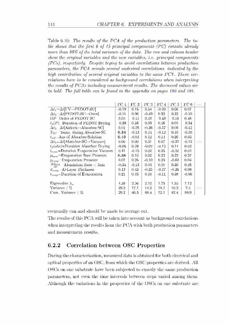
144 CHAPTER 6. EXPERIMENTS AND ANALYSIS
Table 6.10: The results of the PCA of the production parameters. The ta-ble shows that the rst 6 of 15 principal components (PC) contain alreadymore than 89% of the total variance of the data. The row and column headershow the original variables and the new variables, i.e. principal components(PCs), respectively. Despite trying to avoid correlations between productionparameters, the PCA reveals several undesired correlations, indicated by thehigh contribution of several original variables to the same PCV. These cor-relations have to be considered as background correlations when interpretingthe results of PCAs including measurement results. The discussed values arein bold. The full table can be found in the appendix on pages 190 and 191.
PC 1 PC 2 PC 3 PC 4 PC 5 PC 6 · · ·∆t1=∆t[UV→PEDOT-SC] -0.19 0.15 0.54 -0.09 0.06 0.07∆t2=∆t[PEDOT-SC→Oven] -0.11 0.06 -0.49 0.32 0.22 -0.10OP=Order of PEDOT-SC 0.05 -0.11 0.10 -0.43 -0.11 0.48td(P )=Duration of PEDOT Drying -0.39 0.16 0.09 0.16 0.05 -0.34∆t3=∆t[Airlock→Absorber-SC] 0.01 -0.25 -0.26 -0.57 0.09 -0.12TSC=Temp. during Absorber-SC 0.34 -0.13 0.14 -0.12 0.16 -0.50tsol=Age of Absorber-Solution 0.43 -0.01 0.12 0.14 0.26 0.03∆t4=∆t[Absorber-SC→Vacuum] 0.00 0.00 0.51 0.07 -0.22 -0.12 · · ·td(abs)=Duration Absorber Drying -0.06 0.59 -0.02 -0.15 0.14 0.02tevac=Duration Evaporation Vacuum 0.41 -0.15 0.02 0.25 -0.22 0.04pbase=Evaporation Base Pressure 0.38 0.10 0.02 0.22 0.23 0.37pevap=Evaporation Pressure 0.07 0.25 -0.10 0.23 -0.60 0.04∆d5nm
∆t =Aluminium Rate < 5nm -0.34 -0.13 0.03 0.20 0.30 0.45devap=Al-Layer Thickness 0.13 0.43 -0.25 -0.27 -0.26 0.09tevap=Duration of Evaporation 0.21 0.45 0.10 -0.11 0.38 -0.06
Eigenvalue λα 4.38 2.56 2.12 1.75 1.55 1.12Variance / % 29.2 17.1 14.2 11.7 10.3 7.5 · · ·Cum. Variance / % 29.2 46.3 60.4 72.1 82.4 89.9
eventually can and should be made to average out.
The results of this PCA will be taken into account as background correlations
when interpreting the results from the PCA with both production parameters
and measurement results.
6.2.2 Correlation between OSC Properties
During the characterisation, measured data is obtained for both electrical and
optical properties of an OSC, from which the OSC properties are derived. All
OSCs on one substrate have been subjected to exactly the same production
parameters, not even the time intervals between steps varied among them.
Although the variations in the properties of the OSCs on one substrate are
6.2. PRINCIPAL COMPONENT ANALYSIS 145
small (see section 6.1.3), the experimental series showed that the assumption
of all OSCs on one substrate being the same does not hold.
For example, one subtle dierence, which had not been considered before, is
the radial distance of the OSC on a substrate from the centre of the substrate
(see gure 4.8). This is motivated by the nature of the spin-coating process,
during which the lm of absorber solution dries from the centre on outwards,
possibly having an eect on both the optical and electrical properties of an
OSC. Transmission measurements with polarised light have shown a dierent
angle dependence of the transmission at the centre and at the periphery of
a substrate [65]. The eect on the corresponding electronic properties has
yet to be shown. The question is, what is due to statistical variations per
substrate and what can be explained by e.g. the dierence in radial position
of the OSCs?
Thus, a PCA taking only the measured properties of OSCs into account was
carried out and should reveal such correlations, if any. This analysis applies
the observations from all 286 OSCs, trying to nd explanations for the spread
per substrate. Table 6.11 shows the rst ten of 16 principal component
vectors. The meaning of the OSC properties, which were included in the
PCA are described in section 5.3.2. The power conversion eciency is not
included in the analysis, because it is a linear combination of Voc, Jsc and FF .
Fitting the simple diode model to the IV-characteristics (see section 5.3.2)
generally did not yield sensible parameters for the OSCs with a FF below
0.4. Since all OSCs were included in the PCA, the model parameters are
omitted.
PC 1
The rst principal component (46.7% of the variance) is dominated by the
electrical properties of the OSCs as shown with bold in the PC 1 column of
table 6.11. Neither the radial distance to the substrate centre nor the position
of the extrema in the absorption spectrum have a signicant contribution.
However, the correlation between the electronic properties is generally as
expected. The higher the current density at 1V forward bias (J1V ) the lower
the resistance there R1V , which holds both for the dark and the illuminated
case. Vmpp and Jmpp contribute in the same direction, which is expected
from the positive correlation with FF . The higher Rsc, the lower Roc is also
expected for the same reason. It is interesting to note that from the set of the
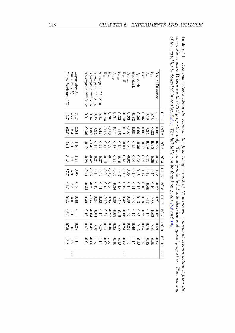
146 CHAPTER 6. EXPERIMENTS AND ANALYSIS
Table
6.11:This
tableshow
salon
gthe
columnsthe
rst
10of
atotal
of16
principal
compon
entvectors
obtained
fromthe
correlationmatrix
Rbetw
eenthe
OSCproperties
only.
The
analysis
inclu
dedboth
electricalandoptical
properties.The
mean
ing
ofthe
variablesisdescribed
insection
5.3.2.The
fulltable
canbe
foundon
pages192
and193.
PC1
PC2
PC3
PC4
PC5
PC6
PC7
PC8
PC9
PC10
···Radial
Distan
ce-0.04
0.060.35
-0.430.72
-0.270.27
-0.020.09
-0.05V
oc
0.18-0.32
0.40
-0.29-0.15
0.10-0.38
-0.02-0.06
-0.39J
sc
0.190.24
0.39
0.39-0.12
-0.46-0.17
0.150.16
-0.12F
F0.35
0.06-0.17
0.020.05
0.100.18
-0.220.05
0.02J
1Vdark
0.29
0.09-0.30
0.050.18
0.170.15
0.58-0.13
-0.43R
1Vdark
-0.33
0.000.23
0.06-0.10
0.21-0.02
0.140.46
0.15J
1Vill
0.33
-0.070.06
-0.020.05
0.180.00
0.540.24
0.34R
1Vill
-0.32
0.14-0.04
0.13-0.10
0.120.32
-0.060.23
-0.65···
Vm
pp
0.33
-0.160.13
-0.16-0.07
0.13-0.19
-0.15-0.09
-0.23J
mpp
0.31
0.170.17
0.25-0.05
-0.240.09
-0.050.25
-0.10R
sc
0.30
-0.130.09
-0.11-0.13
0.340.35
-0.270.46
0.05R
oc
-0.33
-0.130.17
-0.14-0.05
0.14-0.10
0.370.14
-0.07Absorp
tion1
stMin
0.020.42
0.22-0.37
-0.420.01
0.220.14
-0.290.10
Absorp
tion1
stMax
0.030.54
0.13-0.21
-0.130.19
0.04-0.04
-0.070.02
Absorp
tion2
ndMin
0.040.30
-0.46
-0.42-0.02
-0.21-0.47
-0.040.47
-0.08Absorp
tion2
ndMax
0.01-0.39
-0.17-0.28
-0.41-0.54
0.390.16
0.07-0.01
Eigen
value
λα
7.472.94
1.461.23
0.950.56
0.480.33
0.250.13
Varian
ce/%
46.718.4
9.17.7
5.93.5
3.02.1
1.60.8
···Cum.Varian
ce/%
46.765.0
74.181.8
87.791.3
94.396.3
97.998.8
6.2. PRINCIPAL COMPONENT ANALYSIS 147
main OSC parameters Voc, Jsc and FF , only FF has a considerable inuence
on PC 1, whereas both Voc and Jsc contribute less. This is not surprising,
because Voc and Jsc are not governed to the extent by, e.g. interface barriers,
as is FF .
PC 2
The largest contributions to PC 2 (18.4% of the variance) come from the
extrema of the absorption spectrum. Voc and Jsc, which had the least in-
uence of the electronic parameters on PC 1, are the electronic parameters
with the largest inuence on PC 2. Again the radial distance of the OSCs
to the substrate centre has only negligible inuence. The extrema of the
absorption show an interesting behaviour. Whereas the rst three extrema
being observed at small wavelengths exhibit the same trend, the forth ex-
tremum (second maximum) shows the opposite trend. The rst minimum is
associated with the lm thickness of the absorber layer, as shown by optical
simulations [65]. However, the shift of the other extrema has not yet been
analysed systematically. If indeed these extrema show the same trend in the
optical simulations, more than the rst absorption minimum could be used
for determining the layer thickness, increasing the quality of the thickness
estimations. Assuming that the rst absorption minimum is a measure of
the absorber layer thickness, the correlations with Voc and Jsc indicate that
the thicker the OSCs, the lower the Voc, but the higher Jsc. The absorber
thickness was in the range of 80nm, a region, where optical simulations show
that a further increase of Jsc is possible up to 90nm due to increased light
harvesting. This agrees with the discussed PCA. The Voc however decreases
with increasing absorber layer thickness in the range obtained. A reduction
of Voc with increasing thickness of the absorber layer is sometimes reported
in literature, but has not seen in the OSCs made by our group so far.
PC 3
PC 3 (9.1% of the variance) has four contributions with an absolute value
of more than 0.3: the radial distance of the OSC to the substrate centre
(0.35), Voc (0.40), Jsc (0.39) and the second absorption minimum (-0.46). PC
3 is the rst PC on which the radial distance has a signicant contribution.
It suggests that an increase of the distance to the centre of the substrate
correlates with an increase of the two electronic parameters (Voc and Jsc)
148 CHAPTER 6. EXPERIMENTS AND ANALYSIS
and a decrease in the position of the second absorption minimum. The fact
that only one of the absorption extrema contributes signicantly to PC 3
is surprising. The position of the second minimum varies between 435 and
459nm. However, the maximum observed dierence in polarised transmission
is in between 500 and 600nm [65]. Thus rather a dependence with the second
absorption maximum, which lies in this region, would be expected, if the
observed dierence in polarised transmission has an eect on the electrical
properties. This has to be further investigated with absorption, polarised
transmission and IV measurements on a new set of substrates.
Other Observations
PC 5 (5.9% of the variance) has three dominant contributions larger than
0.4: the radial distance (0.72), the position of the rst (-0.42) and second
absorption maximum (-0.41). At rst sight, this trend seems contradicted
by the corresponding values on PC 4. However, in 0th order approximation
the three mentioned parameters dominate PC 5, whereas there are other
parameters on PC 4 which need to be taken into account as well, e.g. an
lowering of the position of the 2nd absorption minimum. The analysis takes
place in a 16-dimensional space and all signicant contributions have to be
taken into account. Otherwise, the chosen direction based on only a few
dominant contributions to a PCV deviates too much from the actual PCV.
Furthermore it is likely that the PCs from PC 4 and onwards cover the noise
in the data, rather than real pattern by virtue of their small eigenvalue.
Conclusions
• The FF correlates strongly with the electrical properties (all with abso-
lute contributions above 0.29) on the rst principal component (46.7%
of the variance). However, there are two notable exceptions: the Voc
and the Jsc. This is as expected, because Voc and Jsc are less aected
by interface barriers, which have a stronger inuence on the other elec-
trical properties.
• Voc and Jsc correlate more with the optical properties, which are found
on the second PC, containing nearly 20% of the data variance. Since
the optical properties can be used as measure of the absorber lm
thickness, Voc and Jsc appear to depend on the device thickness, rather
6.2. PRINCIPAL COMPONENT ANALYSIS 149
than the interface barrier, which aects FF . The eect of dierent
absorber layer thickness has to be investigated further, but as rst
approximation it can be said that Jsc raises and Voc falls with increasing
absorber layer thickness. This behaviour is claimed by some groups,
but has not been observed in our group before.
• The radial distance has its rst signicant contribution to PC 3 (only
9.1% of the variance). The rst two PCs have little contribution of
the radial distance of the OSCs on a substrate, indicating that more
than 65% of the variance in the data can be explained by statistical
variations.
• Considering PC 3, the higher the radial distance, the higher Voc and
Jsc, but at the same time the second absorption minimum shifts to
shorter wavelength. The origin of this behaviour has not been found
yet. The shift of only the second absorption minimum might indicate
a changed absorption at 450nm, which in turn can aect Voc and Jsc.
This has to be investigated with optical simulations of the absorption
spectrum.
6.2.3 Correlations between Production Parameters andη
Although only few parameters were varied during the production of the
OSCs, as shown in section 6.1.2, the obtained OSC properties have a consid-
erable spread, e.g. FF varies between 0.29 and 0.50. The main phenomena
and their underlying physics in the measured OSCs were previously dis-
cussed, but the production parameters causing the spread, have yet to be
identied. In order to assess the inuence of the production parameters on
the OSC performance, a PCA was carried out with the above described set of
15 production parameters and the key solar cell property, namely the power
conversion eciency η. All OSCs on a substrate saw the same process param-
eters and therefore the analysis was done substrate-wise using the average η
per substrate. This furthermore gives every substrate the same weight in the
analysis, despite some substrates having dierent number of working OSCs
(due to defects described in section 5.3.1).
All production parameters, which were introduced in section 6.1.1, were in-
cluded into the analysis. The PCA is a linear method and in order to locally
150 CHAPTER 6. EXPERIMENTS AND ANALYSIS
approximate complex non-linear system it needs as many parameters as are
thought to be inuential. If any of the chosen parameters does not have a sig-
nicant inuence on η, they will appear in the PCA with little contribution
to the rst principal component vectors (PCVs).
The rst 10 of 16 PCVs are shown in table 6.12. The table also lists the
eigenvalue λα, the percentage of variance and the cumulated values for each
principal component near the end of the table. The last line in the table
shows the absolute value of the product of the contribution of the variable η
to the PC and the eigenvalue of the PC, i.e. |η λα|. The rst six PCs contain
together already nearly 90% of the variance of the data. Including the PCs
up to PC 10 can account for nearly 100% of the variance.
From a simple system one would expect that most properties are governed
by fewer PCs. However, this is not the case and at least seven of the 16 PCs
are necessary to capture more than 90% of the variance. There appears to be
no clear cut tendency and detective work and physical intuition is necessary
to make sensible inferences from the data.
PC 1
The rst principal component contains most of the variance in the data
(27.4%), but only a very weak contribution from η (-0.01). Comparing this
PCV to the rst principal component vector of the PCA on the production
parameters (table 6.10) shows that both are nearly equal. This and the
fact that η contributes little to PC 1, indicates that PC 1 contains only the
correlations between production parameters which do only little correlate
with the variable η. Therefore using only the eigenvalue λα is not an adequate
measure for assigning the relevance of a PC for the interdependence between
production parameters and η.
One approach for assigning a measure of relevance would be to consider the
absolute value of the product of a PC contribution to η and the PC eigenvalue
λα, i.e. |η λα|. Ranking according to this weighted λα would allow an ordering
of the PCs with respect to their inuence on η. The order of the three most
relevant PCs for η is then PC 2, PC 4 and PC 3 in descending order. These
PCs show both a large λα anf signicant contributions from the variable η.
PC 1 follows according to this ranking only on position 9.
The high correlation between the production parameters again stresses the
need to consider the background correlations, i.e. the results of the PCA
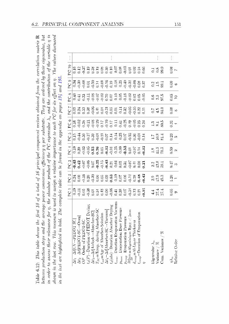
6.2. PRINCIPAL COMPONENT ANALYSIS 151
Table6.12:Thistableshow
stherst10
ofatotalof
16principalcomponentvectorsobtained
from
thecorrelationmatrix
Rbetweenproductionstepsandtheaveragepower
conversione
ciency
ηpersubstrate.
Theyareorderedby
theireigenvalue,but
inorderto
assess
theirrelevance
for
η,theabsolute
product
ofthePCeigenvalue
λαandthecontribution
ofthevariable
ηis
show
nin
thelastrow.Thismeasure
isusedto
assign
arelative
importance
toeach
PCforitseecton
η.The
values
discussed
inthetext
arehighlightedin
bold.The
completetablecanbe
foundin
theappendixon
pages194and195.
PC1
PC2
PC3
PC4
PC5
PC6
PC7
PC8
PC9
PC10
···
∆t 1=
∆t[UV→PEDOT-SC]
-0.19
0.24
-0.43
-0.19
0.15
0.16
0.03
-0.40
-0.34
0.16
∆t 2=
∆t[PEDOT-SC→Oven]
-0.11
0.00
0.42
0.20
-0.44
-0.02
0.24
0.41
-0.30
0.12
OP=Order
ofPEDOT-SC
0.05
-0.16
-0.07
-0.03
0.50
0.38
0.53
0.33
-0.08
-0.37
t d(P
)=Duration
ofPEDOTDrying
-0.38
0.20
-0.06
-0.05
-0.17
-0.21
0.38
-0.11
0.01
0.19
∆t 3=
∆t[Airlock→Absorber-SC]
0.01
-0.20
0.07
0.53
0.39
-0.08
-0.06
-0.08
-0.50
0.38
TS
C=Tem
p.duringAbsorber-SC
0.34
0.00
-0.25
0.26
-0.01
-0.29
0.41
-0.07
0.14
0.18
t sol=Age
ofAbsorber-Solution
0.43
0.05
-0.15
0.05
-0.21
0.17
0.04
-0.02
-0.01
0.08
∆t 4=
∆t[Absorber-SC→Vacuum]
0.00
0.09
-0.43
-0.32
0.07
-0.19
-0.21
0.70
-0.16
0.30
t d(a
bs)=
Duration
Absorber
Drying
-0.06
0.53
0.21
-0.01
0.14
0.17
0.05
0.07
0.19
0.10
···
t evac=Duration
EvaporationVacuum
0.41
-0.19
-0.01
-0.23
-0.14
-0.11
0.01
-0.10
-0.18
-0.07
pbase=EvaporationBasePressure
0.38
0.07
0.03
-0.09
-0.23
0.41
-0.11
-0.05
-0.25
0.08
pevap=EvaporationPressure
0.07
0.06
0.31
-0.53
0.07
-0.25
0.32
-0.16
-0.40
-0.03
∆d5
nm
∆t
=Aluminium
Rate<5nm
-0.34
-0.12
-0.07
0.01
-0.25
0.49
-0.05
-0.02
-0.22
0.01
devap=Al-Layer
Thickness
0.13
0.28
0.41
-0.07
0.36
-0.05
-0.35
0.02
-0.06
0.02
t evap=Duration
ofEvaporation
0.21
0.48
0.00
0.14
-0.01
0.23
0.22
0.05
0.08
0.24
η-0.01
-0.42
0.21
-0.32
0.14
0.24
0.11
-0.05
0.37
0.66
Eigenvalue
λα
4.4
2.9
2.2
1.8
1.7
1.3
0.7
0.6
0.2
0.1
Variance
/%
27.4
17.9
13.8
11.5
10.8
8.1
4.5
3.5
1.5
0.8
···
Cum.Variance
/%
27.4
45.3
59.1
70.5
81.4
89.5
94.0
97.5
99.1
99.9
|ηλ
α|
0.05
1.20
0.47
0.59
0.23
0.31
0.08
0.03
0.09
0.08
···
RelativeOrder
91
32
54
810
67
152 CHAPTER 6. EXPERIMENTS AND ANALYSIS
with only production parameters (table 6.10), when interpreting the results
of this PCA.
PC 2
td(abs) ↑ ∧ tevap ↑ ∧ η ↓
The three highest contributions to PC 2 (17.9% of the variance) are the
duration of absorber drying (td(abs), 0.53), the time it took to evaporate the
Al cathode (tevap, 0.48) and the power conversion eciency η (-0.42). As 0th
order approximation, i.e. when only considering the dominant contributions,
this suggests in that increasing both parameters, results in a decrease of η.
Notable changes compared to the background correlations (table 6.10) are
seen in the temperature during absorber spin-coating (TSC , -0.13→0.00), the
evaporation pressure (pevap, 0.25→0.06) and the Al-layer thickness of the
cathode (devap, 0.43→0.28).
The duration of the absorber drying in vacuum (td(abs)) and η appear to
correlate negatively. However, it has to be kept in mind that this contribu-
tion was slightly higher in the PCA with production parameters only (0.59),
making it most likely an artefact from the production process. The nega-
tive correlation is counter-intuitive, because one would assume that after a
longer drying time of the absorber, less solvent molecules are left. The sol-
vent used, o-dichlorobenzene (DCB), has a high boiling point of 180.5C and
it is expected that despite the very thin spin-coated layer (≈ 80nm), the lm
contains residual solvent. The absorber layer of all substrates were dried in
a vacuum lock for more than 23h at a pressure <0.1bar and subsequently
put into the high vacuum (<10−5mbar) of the evaporation chamber for more
than 14h. Measuring the change in weight of a substrate due to the evapo-
ration of the solvent is below the detection limit of the available equipment
(<0.01mg). There is no unanimous opinion on the importance of this pa-
rameter between the research groups working on OSCs. Whereas Li et al.
carefully state that a longer drying might be benecial due to the removal
of residual solvent, other research groups built good OSCs from the same
materials despite of drying less than 3h [97]. Most research publications on
OSC do not state the time of drying.
The second largest contribution to PC 2 is from the duration of the cathode
evaporation (tevap). During the evaporation process, the absorber layer is
6.2. PRINCIPAL COMPONENT ANALYSIS 153
exposed to the aluminium atoms evaporating from a resistively heated tung-
sten boat. The other parameters associated with the evaporation process
have much less inuence on PC 2. Even the deposition rate of the rst 5nm
aluminium (∆d5nm
∆t), i.e. the rate at which the rst hot Al-atoms are deposited
onto the absorber layer, has little inuence, although this is the only time
when the atoms directly impact on the absorber layer. After 5-10nm the
Al-layer is closed and furthermore begins to act as mirror to the IR-radiation
from the evaporation source. Still, it is known from experience that sub-
strates, which had been exposed to a long evaporation step, tend to have
a lower η, making thermal eects the most likely cause. The evaporation
chamber is not equipped with a thermometer, but estimations for the heat
transfer can be made. Under the assumption that the evaporation source
can be approximated as black body (emissivity=1), an order of magnitude
estimation of the total energy radiated per unit surface area in unit time jE
can be obtained via the Stefan-Boltzmann-law
jE = σsbT4, (6.5)
where σsb is the Stefan-Boltzmann constant and T the temperature of the
black body. At the evaporation base pressure of approximately 10−5mbar, the
boiling point of aluminium is about 1100K. The area of the glowing tungsten
boat is circa 1cm2, thus the radiated power into the half-sphere amounts
to roughly 10W. The perpendicular distance between radiating surface and
substrates is approximately 20cm, so that the received irradiance per cm2
is about 25mW, i.e. small. Most of this power is even reected by the
substrate as soon as Al-layer is closed. The second cause for an increase in
temperature of the substrate is the latent heat during condensation of the
Al (10.9 kJ/g) and the subsequent crystallisation (397 J/g). Assuming a
100nm thick Al layer, a rough estimate of the latent heat amounts to an
energy of about 0.3J per cm2, which is distributed during the 5 to 15min of
evaporation. This contribution is indeed very small as well. Why the long
evaporation has a negative inuence is not clear at the moment. The PCA
and general experience from the laboratory exhibit the same tendency, i.e. a
longer evaporation step is reducing η. To completely rule out thermal eects
an installation of a thermocouple inside the evaporation chamber is planned,
but could not be carried out within the time of this thesis.
It is interesting to note that the temperature during absorber spin-coating
154 CHAPTER 6. EXPERIMENTS AND ANALYSIS
(TSC) has no inuence on PC 2 when the PCA includes η, but contributed
0.12 to PC 2 of the background correlations. Also the contribution of the
pressure during cathode evaporation (pevap) drops from 0.25 to 0.06 and the
contribution of the thickness of the absorber layer (devap) is substantially
reduced. Although physical explanations can be found, one has to be careful
when deducing a causal dependence from the PCA by considering the changes
with respect to the background correlations, because all 16 dimensions, i.e.
variables have to be considered.
PC 3
∆t1 ↓ ∧ ∆t2 ↑ ∧ ∆t4 ↓ ∧ η ↑
Considering |η λα| PC 3 is on position 3 of relative importance (13.8% of
the variance). The three highest contributions on PC 3 are the time interval
between UV-Ozone treatment of the substrates and spin-coating of the PE-
DOT:PSS layer (∆t1, -0.43), the time interval to the subsequent drying of the
PEDOT:PSS layer in the oven (∆t2, 0.42) and the time interval between spin-
coating of the absorber layer and its drying in vacuum (∆t4, -0.43). η has a
contribution of 0.21. However, all three production parameters were higher in
the background correlations and their contribution was only slightly reduced
when including η in the analysis. Thus no rm deductions can be made, be-
cause these correlations appear to be artefacts from the production process.
The fourth highest contribution, the thickness of the aluminium layer (devap),
however exhibited a strong increase in is absolute value (-0.25→0.41).
An important fact on PC 3 is the change in sign of the dominating corre-
lations with respect to the background correlations. Furthermore a large
increase of the contributions of the duration of absorber drying (td(abs), -
0.02→0.21) and the evaporation pressure (pevap, -0.10→0.31) as compared
to the background correlations. The correlation of the evaporation pressure
with η has the same trend as to PC 4. The duration of absorber drying
suggests a longer time is benecial for η, apparently contradicting its con-
tribution on PC 2. However, it has to be kept in mind that the PCVs of
PC 2 and PC 3 are perpendicular and thus pointing into dierent directions.
If the proposed methodology of interpretation, i.e. taking into account the
changes with respect to the background correlations, proves to be valid, then
the inuence of the absorber drying to PC 3 would be considered stronger
6.2. PRINCIPAL COMPONENT ANALYSIS 155
on η than its contribution to PC 4, because in the latter case it only de-
creased slightly from a value which had been already high in the background
correlations.
PC 4
∆t3 ↑ ∧ ∆t4 ↓ ∧ pevap ↑ ∧ η ↓
PC 4 (11.5% of the variance) has the second largest value of |η λα| (0.59).
The inuential variables for PC 4 are the time interval between nishing
the drying of the PEDOT:PSS layer and spin-coating of the absorber layer
(∆t3, 0.53), the evaporation pressure (pevap, -0.53), the time between ab-
sorber spin-coating and absorber drying (∆t4, -0.32) and η (-0.32). One
distinct change with respect to the background correlation (table 6.10) is
again that the PC has changed sign for the most prominent contributions,
with some exceptions however: the time interval between UV-Ozone treat-
ment and PEDOT:PSS spin-coating (∆t1) and the subsequent time interval
between PEDOT:PSS spin-coating and its annealing in the oven at elevated
temperatures (∆t2). The contributions to PC 4 collapsed for the order of
PEDOT-SC (OP , -0.43→0.03) and the aluminium evaporation rate <5nm
(∆d5nm
∆t, 0.20→0.01).
The time interval between nishing the drying of the PEDOT:PSS layer
and the spin-coating of the absorber layer (∆t3) has a high contribution on
PC 4, albeit its absolute value is lower than for the background correlations
(0.57→0.53). Thus no sensible deduction can be made, because it appears
to be an artefact from the production process.
The contribution of the evaporation pressure (pevap, -0.53) to PC 4 has the
same sign as the contribution from η, i.e. the higher the pressure during
evaporation, the better η. Its absolute contribution to PC 4 more than
doubled with respect to the background correlations. Generally, the higher
the evaporation pressure, the quicker the evaporation. This is in line with
what has been observed on PC 2 for the duration of evaporation (tevap)
and this trend is known from experience. The two parameters, evaporation
pressure and evaporation duration, appear with a signicant contribution to
two dierent PCs, both essentially stressing that a quick evaporation process
is benecial for η. However, it is interesting to note that the aluminium
evaporation rate <5nm (∆d5nm
∆t), i.e. the rate in which the rst Al-atoms
condense on the absorber surface, has little inuence up to PC 5.
156 CHAPTER 6. EXPERIMENTS AND ANALYSIS
The third signicant inuence is observed for the time interval between spin-
coating of the absorber layer and drying of the substrates in vacuum (∆t4,
-0.32). The longer the delay, the higher the eciency. The substrates are
spin-coated for 90s at 1500rpm. This is longer than it takes for the wet
layer to dry as indicated by a prominent colour change from yellowish to
dark violet. However, for o-dichlorobenzene (DCB) the absorber layer still
contains some residual solvent, when taking the substrate o the spin-coater.
By putting the substrates into vacuum early, the residual solvent is more
rapidly removed, inhibiting further rearrangement of polymer chains and
PCBM molecules. This freezes the morphology in a non-relaxed way. Only
during OSC post-treatment, i.e. at elevated temperatures, the structure can
relax, but not to the extent as it could during the initial drying. Exactly this
has been demonstrated by Li et al. [61]. They spin-coated the absorber layer
from DCB, but stopped before the layer changed its colour. Subsequently,
they varied the speed of solvent evaporation, e.g. by keeping a substrate in a
saturated solvent atmosphere or rapidly removing the solvent by heating the
substrate on a hot plate. The best OSCs were produced on the substrates
on which the absorber layer was allowed to dry most slowly. However, new
experiments did not reproduce the reported behaviour, because all OSCs
exhibited a very rough absorber surface, which was most likely the cause for
the low eciencies.
Other Observations
The temperature during spin-coating of the absorber layer (TSC) shows on
both PC 3 and PC 4 a signicant increase of its contribution when compared
to the background correlations. On PC 3 it changed from 0.14 to -0.25 and
on PC 4 from -0.12 to 0.26. The correlations with η suggest in both cases
that the colder the temperature TSC , the higher η. A lower temperature
leads to a slower evaporation of the solvent, thus to a more advantageous
morphology. This is again in line what has been proposed by Li et al. [61].
The inuence of the time interval between UV-Ozone treatment and PE-
DOT:PSS spin-coating (∆t1) and η, mentioned at the beginning of sec-
tion 6.1, might show on PC 2. There the contribution of the parameter
has increased from 0.15 to 0.24, suggesting that a shorter time interval leads
to a higher eciency. However, this interpretation only includes one variable
and the other variables need to be considered as well.
6.2. PRINCIPAL COMPONENT ANALYSIS 157
As the order of PEDOT:PSS spin-coating was included in the analysis, this
eect should have been picked up by the PCA. Indeed, it can be found
for PC 5, where the absolute contribution increased from 0.11 to 0.50 with
respect to the background correlation, i.e. showing a signicant increase
in contribution upon including η in the analysis. This suggests, as also
seen in gure 6.2, that the second four substrates being spin-coated with
PEDOT:PSS have a higher eciency. However, here again the changes have
to be seen the light of the other parameters as well, and for a 0th order
approximation at least ∆t2, ∆t3 and devap need to be considered.
The highest contribution of η to any PC is observed on PC 10 (0.66). How-
ever, in the light of the small λα (0.1), it is most likely due to articial
correlations with the production parameters and statistical scatter.
The following parameters did not have a signicant contribution to the PCVs,
which were relevant for η as discussed above: the duration of PEDOT Drying
(td(P )) rst appears in PC 7 (4.5% of variance) with a contribution larger
than 0.3. A plot of this parameter with respect to η has been shown in g-
ure 6.2 on the left side. However, already making the deduction from this plot
that td(P ) has no inuence, would have been to early. It shows some scatter
and td(P ) has to be interpreted in the context of all other production param-
eters. The age of the absorber solution (tsol) has a signicant contribution to
PC 1 (0.43), which however only contains correlations between production
parameters. Thus both parameters have only little eect on the power con-
version eciency η within the ranges of values used for the presented PCA
(table 6.2). Their eect will still be monitored in future experiments, but the
present data suggests that little eort in optimising these two parameters in
necessary due to their negligible inuence.
Conclusions
• With 15 production parameters and only 1 OSC property (here η), the
correlations between the production parameters dominate the rst prin-
cipal component (PC 1) of the PCA. Generally, all correlations from
the production parameters have to be taken into account as background
correlations when interpreting the PCA results. It was subsequently
found that the eigenvalue λα of a principal component alone is not an
adequate measure for describing a PC's importance for η. Therefore
the proposed order is based on the product of the contribution of η and
158 CHAPTER 6. EXPERIMENTS AND ANALYSIS
λα to a PC, i.e. |η λα|.
• The contributions to PC 2, which was found to be the PC with the
highest relevance for η, suggest that if the drying time of the absorber
layer and the duration of the cathode evaporation increase, then η is
decreasing. There is no unanimous opinion about the drying time in
literature and a comparison with the background correlations suggests
that it is an artefact from the production process. The eect of a
long evaporation process however, has before been observed to have
an impact on the OSC performance and the PCA conrms this. One
possible origin is thought to be the thermal stress during evaporation,
although a rst estimate of the heat transfer has turned out to be very
low (<30mW/cm2). However, in order to rule out thermal stress as
cause for a decreasing η it is planned to install a thermocouple inside
the evaporation chamber.
• PC 3 is the third most relevant to η. However, the three most dominant
contributions (∆t1, ∆t2, ∆t4) appear to be artefacts from the produc-
tion process. Thus no rm conclusions can be drawn from PC 3.
• The second most relevant PC to η is PC 4. It suggests that a higher
evaporation pressure (pevap) and a longer time between absorber spin-
coating and drying of the absorber (∆t4) are benecial to η. As a higher
evaporation pressure typically implies a shorter evaporation duration,
PC 4 implies the same as PC 2. The second eect, i.e. the eect of ∆t4,
has been observed by another research group [61]. New experiments
could however not reproduce the results.
• Two parameters did not have any signicant contribution to the rst
seven PCs, which are considered most relevant to η: the duration of
PEDOT Drying (td(P )) and the age of absorber-solution (tsol). Both
have in the presented data little inuence on η and can receive less
attention in future experiments.
6.3 Development of a Statistical Model
Based on the principal component analysis (PCA) conducted on this set of
data, a model was developed for the optimisation of the production parame-
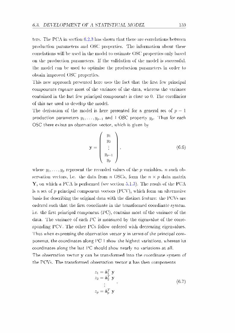
6.3. DEVELOPMENT OF A STATISTICAL MODEL 159
ters. The PCA in section 6.2.3 has shown that there are correlations between
production parameters and OSC properties. The information about these
correlations will be used in the model to estimate OSC properties only based
on the production parameters. If the validation of the model is successful,
the model can be used to optimise the production parameters in order to
obtain improved OSC properties.
This new approach presented here uses the fact that the rst few principal
components capture most of the variance of the data, whereas the variance
contained in the last few principal components is close to 0. The corollaries
of this are used to develop the model.
The derivation of the model is here presented for a general set of p − 1
production parameters y1, . . . , yp−1 and 1 OSC property yp. Thus for each
OSC there exists an observation vector, which is given by
y =
y1
y2...
yp−1
yp
, (6.6)
where y1, . . . , yp represent the recorded values of the p variables. n such ob-
servation vectors, i.e. the data from n OSCs, form the n × p data matrix
Y, on which a PCA is performed (see section 5.1.3). The result of the PCA
is a set of p principal component vectors (PCV), which form an alternative
basis for describing the original data with the distinct feature: the PCVs are
ordered such that the rst coordinate in the transformed coordinate system,
i.e. the rst principal component (PC), contains most of the variance of the
data. The variance of each PC is measured by the eigenvalue of the corre-
sponding PCV. The other PCs follow ordered with decreasing eigenvalues.
Thus when expressing the observation vector y in terms of the principal com-
ponents, the coordinates along PC 1 show the highest variations, whereas its
coordinates along the last PC should show nearly no variations at all.
The observation vector y can be transformed into the coordinate system of
the PCVs. The transformed observation vector z has then components
z1 = aT1 y
z2 = aT2 y
...zp = aT
p y
, (6.7)
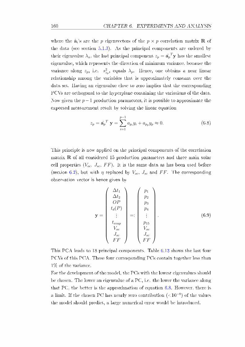
160 CHAPTER 6. EXPERIMENTS AND ANALYSIS
where the ai's are the p eigenvectors of the p × p correlation matrix R of
the data (see section 5.1.3). As the principal components are ordered by
their eigenvalue λα, the last principal component zp = apTy has the smallest
eigenvalue, which represents the direction of minimum variance, because the
variance along zp, i.e. s2zp, equals λp. Hence, one obtains a near linear
relationship among the variables that is approximately constant over the
data set. Having an eigenvalue close to zero implies that the corresponding
PCVs are orthogonal to the hyperplane containing the variations of the data.
Now given the p−1 production parameters, it is possible to approximate the
expected measurement result by solving the linear equation
zp = apT y =
p−1∑i=1
apiyi + appyp ≈ 0. (6.8)
This principle is now applied on the principal components of the correlation
matrix R of all considered 15 production parameters and three main solar
cell properties (Voc, Jsc, FF ). It is the same data as has been used before
(section 6.2), but with η replaced by Voc, Jsc and FF . The corresponding
observation vector is hence given by
y =
∆t1∆t2OP
td(P )...
tevap
Voc
Jsc
FF
=:
p1
p2
p3
p4...
p15
Voc
Jsc
FF
. (6.9)
This PCA leads to 18 principal components. Table 6.13 shows the last four
PCVs of this PCA. These four corresponding PCs contain together less than
1% of the variance.
For the development of the model, the PCs with the lowest eigenvalues should
be chosen. The lower an eigenvalue of a PC, i.e. the lower the variance along
that PC, the better is the approximation of equation 6.8. However, there is
a limit. If the chosen PC has nearly zero contribution (<10−8) of the values
the model should predict, a large numerical error would be introduced.
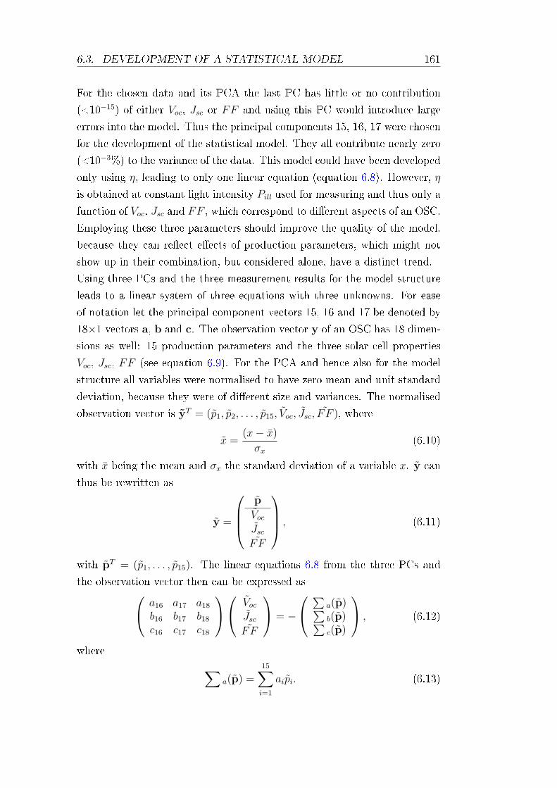
6.3. DEVELOPMENT OF A STATISTICAL MODEL 161
For the chosen data and its PCA the last PC has little or no contribution
(<10−15) of either Voc, Jsc or FF and using this PC would introduce large
errors into the model. Thus the principal components 15, 16, 17 were chosen
for the development of the statistical model. They all contribute nearly zero
(<10−3%) to the variance of the data. This model could have been developed
only using η, leading to only one linear equation (equation 6.8). However, η
is obtained at constant light intensity Pill used for measuring and thus only a
function of Voc, Jsc and FF , which correspond to dierent aspects of an OSC.
Employing these three parameters should improve the quality of the model,
because they can reect eects of production parameters, which might not
show up in their combination, but considered alone, have a distinct trend.
Using three PCs and the three measurement results for the model structure
leads to a linear system of three equations with three unknowns. For ease
of notation let the principal component vectors 15, 16 and 17 be denoted by
18×1 vectors a, b and c. The observation vector y of an OSC has 18 dimen-
sions as well: 15 production parameters and the three solar cell properties
Voc, Jsc, FF (see equation 6.9). For the PCA and hence also for the model
structure all variables were normalised to have zero mean and unit standard
deviation, because they were of dierent size and variances. The normalised
observation vector is yT = (p1, p2, . . . , p15, Voc, Jsc, FF ), where
x =(x− x)
σx
(6.10)
with x being the mean and σx the standard deviation of a variable x. y can
thus be rewritten as
y =
p
Voc
Jsc
FF
, (6.11)
with pT = (p1, . . . , p15). The linear equations 6.8 from the three PCs and
the observation vector then can be expressed as a16 a17 a18
b16 b17 b18
c16 c17 c18
Voc
Jsc
FF
= −
∑a(p)∑b(p)∑c(p)
, (6.12)
where ∑a(p) =
15∑i=1
aipi. (6.13)
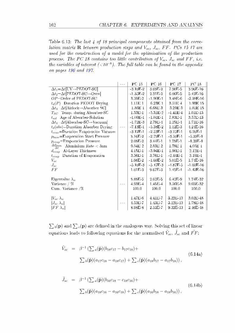
162 CHAPTER 6. EXPERIMENTS AND ANALYSIS
Table 6.13: The last 4 of 18 principal components obtained from the corre-lation matrix R between production steps and Voc, Jsc, FF . PCs 15-17 areused for the construction of a model for the optimisation of the productionprocess. The PC 18 contains too little contribution of Voc, Jsc and FF , i.e.the variables of interest (<10−8). The full table can be found in the appendixon pages 196 and 197.
· · · PC 15 PC 16 PC 17 PC 18∆t1=∆t[UV→PEDOT-SC] -3.10E-2 3.69E-2 7.90E-5 3.96E-16∆t2=∆t[PEDOT-SC→Oven] -1.35E-2 2.31E-2 6.06E-5 5.42E-16OP=Order of PEDOT-SC 3.59E-2 -1.90E-1 3.48E-6 -2.38E-16td(P )=Duration PEDOT Drying 1.11E-1 -6.23E-1 3.51E-4 -1.93E-15∆t3=∆t[Airlock→Absorber-SC] -1.86E-1 6.68E-3 -3.29E-3 -1.81E-15TSC=Temp. during Absorber-SC 1.33E-1 -5.31E-2 -1.41E-4 1.01E-15tsol=Age of Absorber-Solution -1.09E-1 -1.01E-1 7.83E-1 3.57E-13∆t4=∆t[Absorber-SC→Vacuum] -1.72E-3 2.79E-4 1.25E-4 1.71E-16td(abs)=Duration Absorber Drying · · · -7.13E-1 -5.38E-2 1.12E-3 4.24E-16tevac=Duration Evaporation Vacuum -3.12E-1 -2.53E-1 -3.25E-1 6.20E-1pbase=Evaporation Start Pressure 8.16E-2 -2.79E-1 -3.50E-1 -5.39E-1pevap=Evaporation Pressure 2.08E-2 3.44E-1 1.78E-1 -1.20E-1∆d5nm
∆t =Aluminium Rate < 5nm 9.54E-2 2.83E-2 1.78E-1 4.05E-1devap=Al-Layer Thickness 4.15E-1 -3.94E-1 1.90E-1 2.12E-1tevap=Duration of Evaporation 3.56E-1 3.76E-1 -2.44E-1 3.19E-1Voc 1.66E-2 -1.69E-2 5.01E-5 1.74E-16Jsc -5.10E-3 -5.47E-3 -4.87E-5 -1.02E-16FF 1.01E-3 9.67E-3 1.45E-4 -1.42E-16
Eigenvalue λα 8.88E-5 2.62E-5 6.42E-9 1.74E-32Variance / % · · · 4.93E-4 1.45E-4 3.56E-8 9.65E-32Cum. Variance /% 100.0 100.0 100.0 100.0
|Voc λα| 1.47E-6 4.41E-7 3.22E-13 3.02E-48|Jsc λα| · · · 4.53E-7 1.43E-7 3.12E-13 1.78E-48|FF λα| 8.98E-8 2.53E-7 9.32E-13 2.46E-48
∑b(p) and
∑c(p) are dened in the analogous way. Solving this set of linear
equations leads to following equations for the normalised Voc, Jsc and FF :
Voc = β−1 (∑
a(p)(b18c17 − b17c18)+∑b(p)(a17c18 − a18c17) +
∑c(p)(a18b17 − a17b18)) ,
(6.14a)
Jsc = β−1 (∑
a(p)(b16c18 − c18c16)+∑b(p)(a18c16 − a16c18) +
∑c(p)(a16b18 − a18b16)) ,
(6.14b)
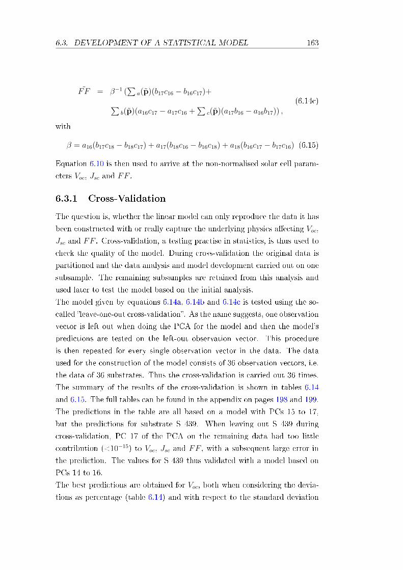
6.3. DEVELOPMENT OF A STATISTICAL MODEL 163
FF = β−1 (∑
a(p)(b17c16 − b16c17)+∑b(p)(a16c17 − a17c16 +
∑c(p)(a17b16 − a16b17)) ,
(6.14c)
with
β = a16(b17c18 − b18c17) + a17(b18c16 − b16c18) + a18(b16c17 − b17c16) (6.15)
Equation 6.10 is then used to arrive at the non-normalised solar cell param-
eters Voc, Jsc and FF .
6.3.1 Cross-Validation
The question is, whether the linear model can only reproduce the data it has
been constructed with or really capture the underlying physics aecting Voc,
Jsc and FF . Cross-validation, a testing practise in statistics, is thus used to
check the quality of the model. During cross-validation the original data is
partitioned and the data analysis and model development carried out on one
subsample. The remaining subsamples are retained from this analysis and
used later to test the model based on the initial analysis.
The model given by equations 6.14a, 6.14b and 6.14c is tested using the so-
called leave-one-out cross-validation. As the name suggests, one observation
vector is left out when doing the PCA for the model and then the model's
predictions are tested on the left-out observation vector. This procedure
is then repeated for every single observation vector in the data. The data
used for the construction of the model consists of 36 observation vectors, i.e.
the data of 36 substrates. Thus the cross-validation is carried out 36 times.
The summary of the results of the cross-validation is shown in tables 6.14
and 6.15. The full tables can be found in the appendix on pages 198 and 199.
The predictions in the table are all based on a model with PCs 15 to 17,
but the predictions for substrate S 439. When leaving out S 439 during
cross-validation, PC 17 of the PCA on the remaining data had too little
contribution (<10−15) to Voc, Jsc and FF , with a subsequent large error in
the prediction. The values for S 439 thus validated with a model based on
PCs 14 to 16.
The best predictions are obtained for Voc, both when considering the devia-
tions as percentage (table 6.14) and with respect to the standard deviation
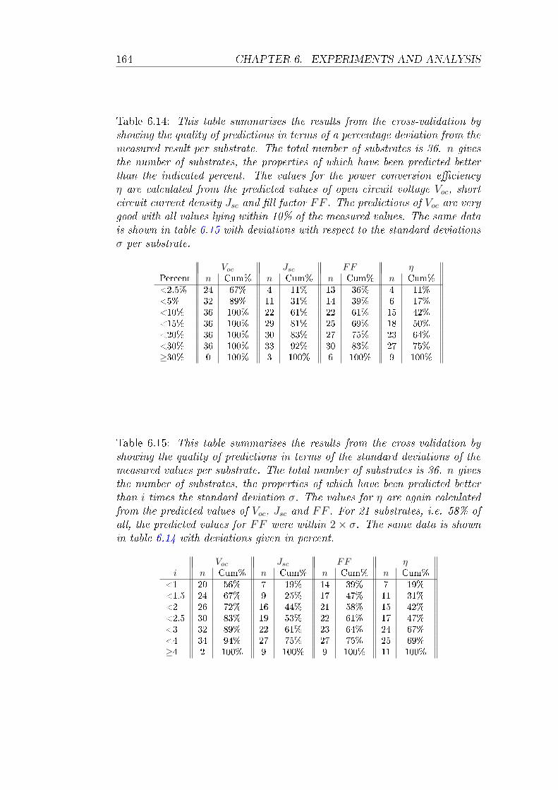
164 CHAPTER 6. EXPERIMENTS AND ANALYSIS
Table 6.14: This table summarises the results from the cross-validation byshowing the quality of predictions in terms of a percentage deviation from themeasured result per substrate. The total number of substrates is 36. n givesthe number of substrates, the properties of which have been predicted betterthan the indicated percent. The values for the power conversion eciencyη are calculated from the predicted values of open circuit voltage Voc, shortcircuit current density Jsc and ll factor FF . The predictions of Voc are verygood with all values lying within 10% of the measured values. The same datais shown in table 6.15 with deviations with respect to the standard deviationsσ per substrate.
Voc Jsc FF ηPercent n Cum% n Cum% n Cum% n Cum%<2.5% 24 67% 4 11% 13 36% 4 11%<5% 32 89% 11 31% 14 39% 6 17%<10% 36 100% 22 61% 22 61% 15 42%<15% 36 100% 29 81% 25 69% 18 50%<20% 36 100% 30 83% 27 75% 23 64%<30% 36 100% 33 92% 30 83% 27 75%≥30% 0 100% 3 100% 6 100% 9 100%
Table 6.15: This table summarises the results from the cross-validation byshowing the quality of predictions in terms of the standard deviations of themeasured values per substrate. The total number of substrates is 36. n givesthe number of substrates, the properties of which have been predicted betterthan i times the standard deviation σ. The values for η are again calculatedfrom the predicted values of Voc, Jsc and FF . For 21 substrates, i.e. 58% ofall, the predicted values for FF were within 2× σ. The same data is shownin table 6.14 with deviations given in percent.
Voc Jsc FF ηi n Cum% n Cum% n Cum% n Cum%
<1 20 56% 7 19% 14 39% 7 19%<1.5 24 67% 9 25% 17 47% 11 31%<2 26 72% 16 44% 21 58% 15 42%<2.5 30 83% 19 53% 22 61% 17 47%<3 32 89% 22 61% 23 64% 24 67%<4 34 94% 27 75% 27 75% 25 69%≥4 2 100% 9 100% 9 100% 11 100%
6.3. DEVELOPMENT OF A STATISTICAL MODEL 165
per substrate (table 6.15). All predicted values are within 10% of the mea-
sured values. However, because the standard deviations for the Voc is always
smaller than 5% (see table 6.5), the quality of predictions in terms of the
standard deviation is lower. Still, predictions of Voc, which are within 10%
of the measured value for all OSCs, and 56%<1σ are very good, given the
spread in the production data. This also indicates that the main parameters
responsible for the variations in Voc are included in the PCA.
The quality of the predictions for Jsc and FF is not as good as compared
to the Voc predictions when considering the percentage dierence between
predicted and measured value only. However, the standard deviations per
substrate are larger than they are for the Voc described by reasons in sec-
tion 6.1.3. Assuming that the model reects the underlying physics, there
are most likely parameters, which were not included in the analysis, but have
an eect on Jsc and FF . The necessity of including the parameter OP into
the analysis shows that the variations in humidity during PEDOT:PSS spin-
coating, which had not been monitored, might have an inuence. Another
parameter, which is known to have an inuence on Jsc is the morphology
of the absorber layer. It should largely depend on the production parame-
ters, but is dicult to be assessed directly for every OSC. It is also currently
not possible to parameterise the morphology, which would be necessary to
include it into the analysis.
Not surprisingly, the predictions for the power conversion eciency η which
are calculated from Voc, Jsc and FF , are deviating from the actual values,
because the dierences add up (see tables 6.14 and 6.15). Still the results
are encouraging, not only if one considers that the model is based on just 36
substrates. Although 36 substrates are a large number comparing to what
is typically published in literature, the experiments will need to continue to
create a large data base.
Summary
• A linear model for Voc, Jsc and FF was developed on basis of the
PCA. It uses the fact that the last principal components have near
zero variance, indicating a linear relationship between the variables.
• The cross-validation of the developed statistical model can reproduce
the OSC properties well, given the small data set. Especially the pre-
166 CHAPTER 6. EXPERIMENTS AND ANALYSIS
dicted values for Voc look promising as all are within 10% of the actual
values. This suggesting that the main production parameters with an
inuence on Voc are included in the model.
• The larger discrepancies between predicted and actual values for Jsc and
FF (21 of 36 substrates predicted <10% from actual values) suggest
that one or more underlying parameters, which leads to variations,
have not yet been included in the PCA. Possible candidates are the
humidity during PEDOT:PSS spin-coating, which will be monitored
in future, and the morphology the absorber layer, which is dicult to
parameterise and capture in the PCA.
• Removing substrates from the data base used for the model reduces the
quality of predictions, suggesting that the number of substrates (36) is
at the lower limit of substrates necessary to construct the statistical
model.
• The quality of the model has to be veried with new experiments, which
are currently being planned.
6.3.2 Outlook: Optimisation of the Production Process
Based on the model, a method for the optimisation of the production pro-
cess is proposed. The model structure developed in section 6.3 gives linear
equations for Voc, Jsc and FF (equations 6.14a to 6.14c and equation 6.10).
The power conversion eciency η, i.e. the value which should be optimised,
is given by
η = FFVoc Jsc
Pill
, (6.16)
where Pill is the intensity of the incident light. Equation 6.16 has to be
optimised subject to certain boundary conditions. The boundary conditions
should be chosen such that the parameters can only move within the limits,
in which the experiments were carried out (see table 6.2). Outside this range,
the model will most likely fail. Furthermore the order of the PEDOT:PSS
spin-coating should be xed, because the detrimental eect of separating a
batch into 2x4 substrates has been shown. Variations in this parameter can
be avoided by using a dierent airlock for the second four substrates.
6.3. DEVELOPMENT OF A STATISTICAL MODEL 167
Using equations 6.14a, 6.14b and 6.14c and keeping in mind that∑
a(p),∑b(p) and
∑c(p) are functions of pT = (p1, . . . , p15)
arg maxp
η(p) = FF (p)Voc(p) Jsc(p)
Pill
, (6.17)
has to be solved. This leads to a set of equations that has to be satised in
order to arrive at an extremum
∂η
∂pi
= 0; i = 1, . . . , 15. (6.18)
The equation 6.17, of which the maximum has to be found, describes a
surface in a 15-dimensional space. The optimisation of equation 6.17, i.e. the
search for a maximum, could be carried out with the Levenberg-Marquardt
Algorithm (section 5.1.2). The boundaries are given by the range of the
production parameters used during this experimental run, i.e. a solution is
searched within the used parameter range. The optimisation should yield a
set of production parameters, which will lead to an OSC with an optimised
power conversion eciency η.

168 CHAPTER 6. EXPERIMENTS AND ANALYSIS
Chapter 7
Outlook
During the course of this thesis the fundamental requirements for a sound
statistical analysis of organic solar cells (OSCs) were developed. Furthermore
the principal component analysis was presented as multivariate method to
search for pattern in the data, with a particular focus on the correlations
between production parameters and OSC properties.
Production Process
The structuring and standardisation of the OSC production process revealed
more than 40 dierent production parameters, which are now routinely re-
corded for every substrate. Obtaining a standardised set of production pa-
rameters made a comparative OSC production possible. However, the PCA
and the developed statistical model also showed that there are apparently
inuential parameters, which have not been monitored yet.
The PCA has identied the duration of the manual evaporation process as
inuential parameter, but the physical origin has yet to be determined. Al-
though a rst crude estimate of the heat transfer suggests little inuence of
the temperature, it should be at least monitored for some evaporation steps
to have a direct access to this parameter. It should be possible to mount a
small thermocouple inside the evaporation chamber at a similar distance to
the source as the substrates are. Attaching the thermocouple directly to the
substrates is as rst evaluation dicult, because the substrates continuously
rotate during evaporation. If however, the temperature is identied as im-
portant production parameter during a PCA, it would be advantageous to
measure the temperature at the substrates. The other related process pa-
rameters, e.g. the evaporation pressure, are already monitored more closely.
169
170 CHAPTER 7. OUTLOOK
However, in order to be eventually able to reproduce a good evaporation pro-
cess it is suggested to replace the human factor in the evaporation process
by an automated control of the evaporation process in the long run.
The second parameter, which might be responsible for some observed vari-
ations in OSC properties, especially in the ll factor FF , is the humidity
during the spin-coating outside the glovebox. It is thought to be the cause
of the detrimental eect seen in FF of the four substrates, which were spin-
coated with PEDOT:PSS rst and thus already had cooled down when they
were exposed to ambient air. Thus a hygrometer has already been installed
at the spin-coater used for the PEDOT:PSS spin-coating. The splitting of
a batch of eight substrates into 2×4 substrates for the PEDOT:PSS spin-
coating can be continued, but the exposure to ambient conditions of the
already cooled down substrates has to be avoided by using a dierent airlock
in future.
One issue, which has not received any attention during this thesis, but would
be paramount is making dierent P3HT:PCBM absorber solutions compa-
rable. The ltering of an absorber solution has become an integral part of
the solution preparation process, because it removes particles otherwise de-
teriorating the quality of the absorber layer. However, during ltering, an
unknown part of the P3HT and the PCBM is also held back by the lter, the
amount of which varies. Even though two solutions were prepared from the
same master solution, it was found that their absorption spectra diered in
peak heights for the absorption peaks of P3HT and PCBM. This indicates a
dierence in the ratio between P3HT and PCBM. Developing a measure to
account for these dierences would make the two solutions comparable and
thus the OSCs made from these solutions. This would to substantially in-
crease the number of OSCs for which comparable production parameters can
be recorded. Features of the absorption spectra, e.g. the relative peak height
of the peaks of P3HT and PCBM, could be used as preliminary parameters.
It received no attention in this thesis, because all OSCs which were presented
were made from exactly the same absorber solution, which had been ltered
once.
Automation of Measurement Methods
The automation of the measurement methods has been paramount for the
reliable characterisation of the OSCs. The automated setup has been planned
171
and designed versatile from the beginning such that there is room for further
extensions.
At the time of writing, the error in the spectral response (SR) measurement,
which made the measured data only useful for qualitative comparison, has
unfortunately not been found yet. Resolving this issue and reconciling the re-
sults for the short circuit density obtained from the SR measurement and the
current-voltage measurement should receive the highest priority. The data
of the SR measurement is very important, because it contains information
about both the absorption and the charge carrier transport. Together with
the absorption measurement and optical simulations, it would be possible to
calculate the internal quantum eciency (IQE), i.e. assessing eciency of
exciton dissociation and charge carrier transport.
The four-wire conguration ensures a high accuracy in the measured voltage
across an OSC. In order to achieve a similar accuracy in the measured current
densities, it is suggested to include an accurate checking of the photovoltaic
area of each OSC. A visual inspection of every OSC is currently done, but
it is not possible to quantify the loss in photovoltaic active area, if the mis-
alignment of bottom and top electrode happens to be outside the built-in
tolerances of the substrate layout. For an accurate measurement of the pho-
tovoltaic active area, it would be necessary to obtain a high resolution image
of each OSC. Using a microscope is not practical due to several reasons, e.g.
the substrate had to be removed from the glovebox and exposed to ambient
conditions leading to a degradation of the OSCs. The most practical solution
would be the integration of a small digital camera on the XY-table, which
can obtain high resolution pictures of each substrate. The XY-table provides
sucient room and including the imaging into the LabView program should
be straight forward due to the modular design of the program. With the help
of imaging software, which could use the optical markers already present on
the used substrates, it should be possible to obtain a very accurate value
for the photovoltaic active area of each OSC. This then can be used to scale
the measured current I to the current density J , an intensive OSC property.
Furthermore, obtaining a picture of all substrates would be of great help in
assessing the quality of the spin-coated layer and make data cleaning more
reliable through a better categorisation of damaged solar cells.
172 CHAPTER 7. OUTLOOK
Electronic Laboratory Notebook
The electronic laboratory notebook (ELN) unites production protocols and
measurement data of all OSCs made in our lab, making an ecient access
and linking of the data inside the ELN possible. The measured data is
currently analysed for about 15 OSC properties. However, there is clearly
more information in the measured data, the aggregation of which was not
possible during the course of this thesis.
The log-plots of the representative dark IV-curves were shown during the
analysis of the main physical phenomena observed during the analysis. Dis-
tinct changes can be observed going from non-annealed to annealed OSCs
on the same substrate and between OSCs on dierent substrates. However,
tting a two diode model to the measured data did not yield acceptable ts.
Thus until a suitable model is in place to describe the dark IV-curves, phe-
nomenological characteristics, e.g. the slope before and after the change in
slope around 0.3V, could be used. It would be especially interesting to in-
vestigate the behaviour of these characteristics upon annealing. Since there
are no optically generated charge carriers in the device, the IV-curve should
only be governed by the interfaces and the morphology of the absorber layer.
During the analysis of the dark IV-curves, it became obvious that the OSCs
all open in reverse bias in a way with can be tted well with a simple expo-
nential function with two parameters (p1, p2)
J = p1 (exp(p2V )− 1) for V < 0V. (7.1)
However, the physical meaning of the parameters, the eect on the forward
bias and their correlation with other OSC properties has yet to be deter-
mined. It is observed that IV-curves with a large opening in reverse bias
generally have a reduced performance. The size of the opening in reverse
changes upon annealing and J at -1V bias is typically reduced by about an
order of magnitude, but it does not disappear.
Optical simulations of the absorption spectrum strongly indicate a linear re-
lation between the position of the rst absorption minimum between 320 and
540nm and the thickness of the absorber layer. First comparisons with values
for the absorber layer thickness obtained by AFMmeasurements conrm this,
but it requires more direct measurements of the absorber layer thickness, e.g.
via AFM, to put the optical determination of the layer thickness on a solid
base. As indicated in the PCA with OSC properties only, the extrema in the
173
absorber spectrum between 320 and 540nm exhibit a particular trend, which
is apparently caused by changes in the absorber thickness. Using more than
just the rst absorption minimum for estimating the absorber layer thickness
should make the method more reliable. Especially for absorber layers exceed-
ing 160nm in thickness, an additional absorption minimum moves from below
into the analysed region.
Data Analysis
The focus of the PCAs performed in this thesis was on attributing the vari-
ations seen in OSC properties to variations during the production process.
During the rst run of experiments all parameters which can be held xed
for all substrates were held xed. This limited the variations to parameters,
which unintentionally varied, yet were monitored. The analysis then showed
the range of variations in OSC properties originating only from the uninten-
tional variations during production, i.e. parameters which varied due the
nature of the process.
It is suggested to conduct another experimental series with more OSC and
in which it should be sought to minimise correlations between production
parameters. Subsequently, the spin-coating speed of the absorber layer is
suggested as rst intentional variation in the production process. Variations
between ωSC=500 to 2000rpm in e.g. ve steps should lead be a sensible
coverage of the parameter range in order to assess the inuence of ωSC on
OSC performance and its reproducibility.
The PCA with 15 production parameters and just one OSC property showed
the large inuence of the correlations between only the production param-
eters. During the interpretation of the PCA result, these correlations were
taken into account as background correlations. However, often drawing rm
conclusions was dicult. Therefore three solutions are suggested, which
should be followed in parallel: (1) reducing the number of unintentional
variations as much as possible, e.g. using a computer-controlled evaporation
process, will lead to a reduction of possible correlations between unintentional
parameter variations, thus leading to big improvements. However there are
some variations, e.g. the time intervals between the production steps, which
will always vary between the substrates of one batch and correlations between
included parameters can still dominate the PCA. (2) Therefore as second
measure a continuous assessment of the correlation between the production
174 CHAPTER 7. OUTLOOK
parameters from batch to batch with the help of the PCA is suggested.
Intentional parameter variation and unintentional ones, as far as possible,
should be adjusted such that their correlations are reduced. (3) Finally, if
there are still substantial correlations between the production parameters,
it is necessary to develop a framework for the interpretation, which takes
the background correlations into account. This would be best done with
simulated data of known correlation. Then the changes in the principal com-
ponent vectors caused by adding an extra variable to variables on which a
PCA has already been carried out could be investigated.
The cross-validation of the model, which has been developed on the basis of
the PCA shows promising results. Especially the predictions for the open
circuit voltage Voc are good, making the presented model the rst model,
which links production parameters and the Voc. The predictions of the short
circuit current density Jsc and the ll factor FF indicate that there are ap-
parently parameters, which have not been included yet. Two parameters,
which should be recorded during production in future are the humidity dur-
ing PEDOT:PSS spin-coating and the temperature during evaporation. Still,
with the present data, the model can be used to nd optimised production
parameters. Using the prediction of Voc, Jsc and FF , the power conver-
sion eciency η can be obtained as function of the production parameters.
However, neither the maximisation of the calculated η nor the testing of the
proposed optimised production parameters could be carried out during the
course of this thesis (see 6.3.2).
One parameter, which is dicult to quantify, but should soon receive a qual-
itative treatment is the eect of the morphology of the absorber layer. Al-
though the morphology should be governed to a large extent by the produc-
tion parameters, it is necessary to quantify the changes in morphology of
the absorber layer in dependence of the production process. A ngerprint of
the morphology could be obtained from the AFM images using specialised
algorithms [98]. Interfaces to the ELN exist and thus these algorithms could
be easily linked to the ELN.
Chapter 8
Conclusions
One of the major goals of research on organic solar cells (OSCs) is the im-
provement of the power conversion eciency η. However, the large variety of
organic semiconductors available and the many production parameters make
a deterministic approach dicult. Statistical methods are required to ana-
lyse the performance of the materials and the reproducibility of OSCs made
with them.
The focus of this thesis is both the development of an experimental plat-
form to permit such a statistical analysis and to subsequently investigate
based on this platform the inuence of the production process on the OSC
performance and reproducibility using principal component analysis (PCA).
The model system used for the experiments is the currently most intensively
investigated OSC system, i.e. devices based on P3HT:PCBM.
The platform consists of a standardised production process, an automated
OSC characterisation setup and a exible, yet ecient, data management
infrastructure. This platform is necessary to acquire an adequate amount of
well-documented OSC production and measurement records, i.e. the prereq-
uisite for any statistical analysis.
Standardisation of the Production Process
To make the production of all OSCs comparable, the production process was
structured and standardised. A set of more than 40 production parameters
has been dened, which is now routinely recorded in a standardised way for
every OSC made in our laboratory. With this data, the complete production
history of an OSC can be traced.
The production parameters were divided into three groups: (1) parameters,
175
176 CHAPTER 8. CONCLUSIONS
which can be controlled well and repeated for any substrate, such as the
spin-coating speed for the organic layers; (2) time intervals, which vary from
substrate to substrate within one batch due to the sequential spin-coating
of each individual substrate; and (3) parameters, which vary due to human
involvement and outside inuences.
Previously only the six parameters of the cathode deposition process (2×pres-sure, layer thickness, rate and 2×duration) had been considered as causes forthe variations in OSC properties, although they had not been investigated
systematically. The remaining four parameters in (3), like the temperature
during spin-coating, were initially assumed to be negligible, but did not turn
out to be so at least for this parameter. The four time intervals of (2) had
not been considered before and were found to have a signicant inuence on
the OSC properties.
Automation of the OSC Characterisation
In addition to well-documented OSC production records, a corresponding
large and consistent pool of measurement data is necessary for the many
OSCs made. Therefore new substrates were developed and all common OSC
characterisation methods were combined into a single multi-purpose auto-
mated measurement setup.
The new substrates are all based on a standardised contact pad structure,
allowing the realisation of dierent layouts, e.g. for up to 10 OSCs, on the
25×25mm2 substrate area. All substrates can be used in the new multiple
mount, which can hold and contact up to nine substrates simultaneously.
Substrates in the multiple mount can be characterised with current-voltage,
spectral response and absorption measurements, which were all integrated
into one automated setup. This combination allows reliable and versatile
OSC characterisation with a high throughput. For example, the current-
voltage characterisation of 90 OSCs at one light intensity can now be carried
out within 90 minutes without any manual interaction, instead of requir-
ing attention every minute. The automated setup additionally provides the
exibility for further extension.
The automation made the measurements less prone to human error and led
to a standardised characterisation cycle. The successful automation of the
main characterisation methods resolved a signicant bottleneck in the exper-
imental cycle, which would otherwise have made the reliable acquisition of
177
the required amount of characterisation data impossible.
Electronic Laboratory Notebook
The logging of more than 40 production parameters and the acquisition of
large amounts of measurement data requires an ecient data management
infrastructure for which an electronic laboratory notebook (ELN) and the
corresponding computational tools were developed.
The ELN unites the data from two dierent sources the user-friendly we-
binterface for the production protocol and the standardised output les from
the automated characterisation and stores them all in a hierarchical struc-
ture. The ecient access and linking of all data within the ELN creates the
basis for the data analysis. The measurement data in the ELN is analysed
and OSC properties are deduced, which are also stored in the ELN.
Parameterisation of the OSC characteristics is necessary to obtain scalar
OSC properties, which can be used for the analysis. For the extraction of
the properties splines have been used for all OSC. No equivalent circuit model
could be found with parameters, which adequately tted the current-voltage
characteristics for ll factors FF below 0.4. This low FF is found in nearly
20% of the made OSCs and its physical origin currently subject to internal
discussion.
Data quality has very high priority, which is ensured by a set of graded
measures. The most important ones are syntax checks at the input stage,
unit testing for the code, which handles the data, and keeping a continuous
history tracking changes inside the ELN. As a result, none of the production
records had to be excluded due to erroneous entries. However, it turned
out that the nal step of data preparation, i.e. the manual pruning of the
measurement data for characteristics which can be explained by defects or
artefacts rather than variations in production parameters, took more than
60% of the time necessary for the data analysis. Of the 360 OSCs made, 21%
had to be sorted out. Automation or semi-automation of this process would
therefore lead to a considerable time saving.
Experimental Results
36 substrates with a total of 360 OSCs were made. During production only
the 15 parameter varied, which due to the nature of the production process
always vary but had yet not been investigated systematically. This was done
178 CHAPTER 8. CONCLUSIONS
to investigate the resulting variations in OSC properties, which need to be
considered when assigning a signicance to the eect of additional production
parameters when varied intentionally.
Despite the standardised production process and keeping the majority of
production parameters xed, the measured OSC properties showed a wider
spread than expected. For a reproducible production process, variations in η
of ±10% around the mean, i.e. here (2.0±0.2)%, would be reasonable, but a
spread of nearly ±50% around the mean was obtained (1.1%≤ η ≤2.8%). Itwas found that the spread in FF , which varied most between the substrates
(0.290.50) was determining η. Already a focus on improving the FF from
the obtained values to 0.6, which is often reported in literature, will lead to
η>3.5%.
The only dierence between the 360 OSCs was in production parameters,
which are hardly mentioned in literature. This places the literature on
P3HT:PCBM OSCs in a new light, where typically only the results of a few
OSCs are presented without showing their signicance. If our observations
hold for the OSC production in other groups as well, both the production
parameters have to be described in more detail and the signicance of the
results has to be shown in publications. Without this information the in-
terpretation of the published results is dicult for the reader. However,
assigning a signicance to eects observed in OSC properties generally re-
quires the investigation of a large number of OSCs. This proves the necessity
of a systematic and statistical approach, the experimental tools of which were
developed as part of the work on this thesis.
Principal Component Analysis
Principal component analysis (PCA) was used as a suitable method in the
search for the production parameter or combination of parameters, which
signicantly contributed to the variations in the observed OSC properties.
A PCA including the 15 production parameters, which varied, and η showed
that the correlation between the production parameters only governed the
behaviour of the largest principal component (PC). These correlations were
taken into account as background correlations during the interpretation of
the PCA results. Furthermore, it was found that the eigenvalue λα of a PC
is not an adequate measure for the importance of a PC for η. λα alone does
not reect the contribution of the variable η to a PC. Therefore |η λα|, i.e.
179
the weighting of λα with the contribution of the variable η to a PC, was
introduced as a new measure of signicance. This led to PC 2, PC 4 and
PC 3 for the three most relevant PCs for η in decreasing order. PC 1 follows
only ninth when ranked by |η λα|.
The results of the PCA1 suggest that within the observed range (300-
900s) an extended duration of the Al-cathode deposition has a negative
impact on η. This is indicated by a negative correlation between the duration
of the vacuum deposition and η (PC 2) and a positive correlation between
the pressure during evaporation (7-13·10−6mbar) and η (PC 3). The latter
parameter is typically higher for shorter deposition times. The results conrm
experience from the laboratory, but the physical origin has yet to be found.
A crude estimation of the heat transfer to the OSCs indicates that thermal
stress is unlikely to be the cause.
The PCA also indicates that it is important to allow the absorber layer to
dry slowly after spin-coating. A longer time interval between absorber spin-
coating and drying of the absorber layer under vacuum (PC 4), and also
a temperature during spin-coating (PC 3 and PC 4) at the lower end of
the range (24-27C), leave more time for the 2-phase system to relax to a
more favourable morphology. This is in line with what is reported in the
literature [61].
It was found that two parameters did not make any signicant contributions
to the rst 7 PCs when ordered according to |η λα|. The age of the absorber
solution (3h to 22 days) and the duration of the PEDOT:PSS drying during
the transfer into the glovebox (46-162min) both have negligible contributions
up to PC 10 (seventh by |η λα|). Hence they can receive less attention in
future.
Although the set of data, which was used for the PCA, was large in term of
what has previously been realised for OSCs in literature, it is at the lower
limit of what is useful for the PCA, because correlations between production
parameters still dominated the results. A new series of experiments should be
planned which will involve more OSCs and in which it is sought to minimise
correlations between production parameters.
On the basis of the PCA conducted, a statistical model was proposed and its
quality tested via cross-validation. The model is used to predict the values of
the open circuit voltage Voc, the short circuit current density Jsc and FF (and
1The corresponding tables with all 18 PCs can be found on pages 194 and 195.
180 CHAPTER 8. CONCLUSIONS
hence η), given the set of 15 production parameters which varied during the
production process. The rst results are promising, e.g. all values for Voc are
predicted within 10% of their measured values. However, the model cannot
account for some variations seen in Jsc and FF , indicating that there are still
parameters which have some inuence on the OSC properties but have not yet
been included in the analysis. Two additional parameters for the production
protocol are proposed: the substrate temperature at the substrate during
cathode deposition and the humidity during PEDOT:PSS spin-coating. The
rst is necessary to assess the thermal inuence directly in order to narrow
down the causes for the detrimental eect of an extended evaporation step.
The second had been found to aect the OSC performance negatively when
the cooled PEDOT:PSS layer was exposed to ambient conditions.
Numerical optimisation of the model, i.e. maximisation of the calculated η,
should yield improved production parameters, but could not be carried out
within time of this thesis.
To summarise, this work created a solid platform for the acquisition and
management of well-documented OSC preparation and measurement records,
the fundamental requirements for sound statistical analysis. PCA was es-
tablished and used to search the data obtained for P3HT:PCBM OSCs for
correlations, in order to explain the large observed spread in the measured
OSC properties. It was found that variations in the evaporation process of
the cathode have a signicant inuence on the OSC properties and it was
conrmed that slow drying of the absorber layer leads to an improved OSC
eciency. Further links between production parameters and OSC properties
were suggested and all necessary tools are in place to allow further investi-
gations of the observed correlations and future material screening and OSC
concept development. On the basis of the PCA, a statistical model was
proposed, which can predict the main OSC properties given the production
parameters. Thus, numerical optimisation of the predicted OSC properties
should lead to improved production parameters, resulting in more repro-
ducible OSCs with better performance.
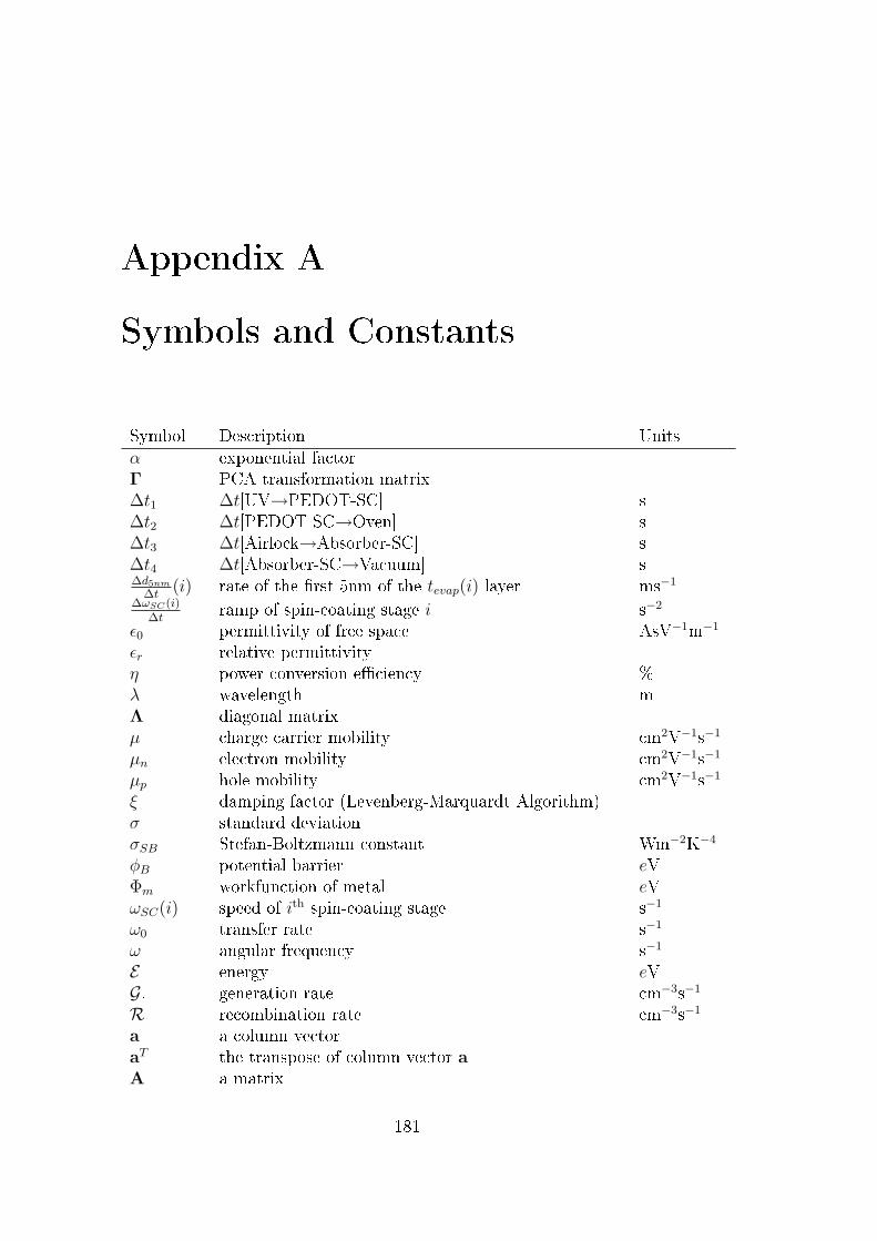
Appendix A
Symbols and Constants
Symbol Description Unitsα exponential factorΓ PCA transformation matrix∆t1 ∆t[UV→PEDOT-SC] s∆t2 ∆t[PEDOT-SC→Oven] s∆t3 ∆t[Airlock→Absorber-SC] s∆t4 ∆t[Absorber-SC→Vacuum] s∆d5nm
∆t(i) rate of the rst 5nm of the tevap(i) layer ms−1
∆ωSC(i)∆t
ramp of spin-coating stage i s−2
ε0 permittivity of free space AsV−1m−1
εr relative permittivityη power conversion eciency %λ wavelength mΛ diagonal matrixµ charge carrier mobility cm2V−1s−1
µn electron mobility cm2V−1s−1
µp hole mobility cm2V−1s−1
ξ damping factor (Levenberg-Marquardt Algorithm)σ standard deviationσSB Stefan-Boltzmann constant Wm−2K−4
φB potential barrier eVΦm workfunction of metal eVωSC(i) speed of ith spin-coating stage s−1
ω0 transfer rate s−1
ω angular frequency s−1
E energy eVG. generation rate cm−3s−1
R recombination rate cm−3s−1
a a column vectoraT the transpose of column vector aA a matrix
181
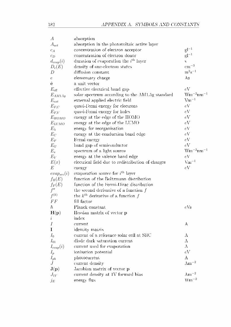
182 APPENDIX A. SYMBOLS AND CONSTANTS
A absorptionAact absorption in the photovoltaic active layercA concentration of electron acceptor gl−1
cD concentration of electron donor gl−1
devap(i) duration of evaporation the ith layer sDe(E) density of one-electron states cm−3
D diusion constant m2s−1
e elementary charge Ase a unit vectorEeff eective electrical band gap eVEAM1.5g solar spectrum according to the AM1.5g standard Wm−2nm−1
Eext external applied electric eld Vm−1
EF,C quasi-Fermi energy for electrons eVEF,V quasi-Fermi energy for holes eVEHOMO energy at the edge of the HOMO eVELUMO energy at the edge of the LUMO eVEλ energy for reorganisation eVEC energy at the conduction band edge eVEF Fermi energy eVEG band gap of semiconductor eVEs spectrum of a light source Wm−2nm−1
EV energy at the valence band edge eVE(x) electrical eld due to redistribution of charges Vm−1
E energy eVevapsrc(i) evaporation source for ith layerfB(E) function of the Boltzmann distributionfF (E) function of the Fermi-Dirac distributionf ′′ the second derivative of a function ff (k) the kth derivative of a function fFF ll factor~ Planck constant eVsH(p) Hessian matrix of vector pi indexI current AI identity matrixI0 current of a reference solar cell at SRC AI01 diode dark saturation current AIevap(i) current used for evaporation AIp ionisation potential eVIph photocurrent AJ current density Am−2
J(p) Jacobian matrix of vector pJ1V current density at 1V forward bias Am−2
jE energy ux Wm−2
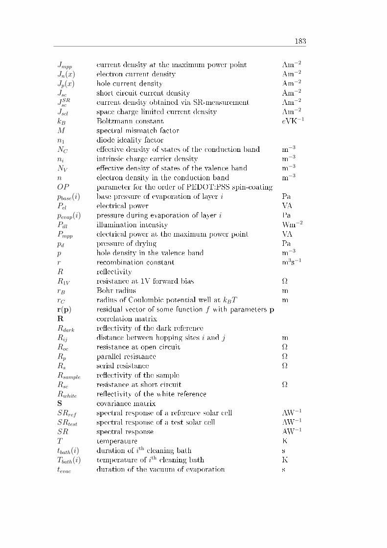
183
Jmpp current density at the maximum power point Am−2
Jn(x) electron current density Am−2
Jp(x) hole current density Am−2
Jsc short circuit current density Am−2
JSRsc current density obtained via SR-measurement Am−2
Jscl space charge limited current density Am−2
kB Boltzmann constant eVK−1
M spectral mismatch factorn1 diode ideality factorNC eective density of states of the conduction band m−3
ni intrinsic charge carrier density m−3
NV eective density of states of the valence band m−3
n electron density in the conduction band m−3
OP parameter for the order of PEDOT:PSS spin-coatingpbase(i) base pressure of evaporation of layer i PaPel electrical power VApevap(i) pressure during evaporation of layer i PaPill illumination intensity Wm−2
Pmpp electrical power at the maximum power point VApd pressure of drying Pap hole density in the valence band m−3
r recombination constant m3s−1
R reectivityR1V resistance at 1V forward bias ΩrB Bohr radius mrC radius of Coulombic potential well at kBT mr(p) residual vector of some function f with parameters pR correlation matrixRdark reectivity of the dark referenceRij distance between hopping sites i and j mRoc resistance at open circuit ΩRp parallel resistance ΩRs serial resistance ΩRsample reectivity of the sampleRsc resistance at short circuit ΩRwhite reectivity of the white referenceS covariance matrixSRref spectral response of a reference solar cell AW−1
SRtest spectral response of a test solar cell AW−1
SR spectral response AW−1
T temperature Ktbath(i) duration of ith cleaning bath sTbath(i) temperature of ith cleaning bath Ktevac duration of the vacuum of evaporation s
184 APPENDIX A. SYMBOLS AND CONSTANTS
Tmix temperature at which solution is mixed Ktpt duration of post-treatment sTpt temperature of post-treatment KtSC(i) dwell of spin-coating stage i sTSC temperature during the spin-coating process KtUV duration of UV-Ozone treatment std duration of drying PaTd temperature of drying Ktsol Age of Absorber-Solution sVbi built-in potential VVmpp voltage at the maximum power point VVoc open circuit voltage VVpt voltage bias during post-treatment VVsol volume of solution used for spin-coating lV0 compensation voltage, V at Jd − Jph = 0 VVd vacuum level oset eVV voltage Vwe mean drift length of electrons mwh mean drift length of holes my(i) observation vector of variable iyi observation vector of sample iy mean of vector yy normalised observation vector with ¯y=0 and σy=1Y observation matrix in terms of original variablesZ observation matrix in terms of principal components
Appendix B
List of Abbreviations
Abbreviation DescriptionA acceptorAFM atomic force microscopyAl aluminiumAM1.5g air mass 1.5 global, the solar standard spectruman annealed, i.e. with post-treatmentCB conduction bandCCD charged-coupled deviceD donorDCB o-dichlorobenzeneDI-water deionised waterDMM digital multi-meterDRY Don't repeat yourselfe electronELB electronic log baseELN electronic laboratory notebookEQE external quantum eciencyFMF Freiburg Materials Research CenterFraunhofer ISE Fraunhofer Institute for Solar Energy SystemsFWHM full width at half maximumGB gloveboxGRP glass-bre re-enforced plasticGUI graphical user interfaceh holeHDF5 Hierarchical Data Format, version 5HOMO highest occupied molecular orbitalID identierIPCE incident photon to converted electron eciencyIQE internal quantum eciencyITO indium-tin-oxideIV current-voltage
185
186 APPENDIX B. LIST OF ABBREVIATIONS
LF laminar owLiF lithiumuorideLMA Levenberg-Marquardt AlgorithmLOTSDSC5 a calibrated reference solar cellLCAO-MO linear combination of atomic orbitals molecular orbitalsLUMO lowest unoccupied molecular orbitalMDMO-PPV poly(2-methoxy-5-(3,7-dimethyloctyloxy)-
-1,4-phenylene vinylene)MO molecular orbitalmpp maximum power pointMySQL an open source database management systemn-QFL electron quasi Fermi levelnan non-annealed, i.e. without post-treatmentOFET organic eld eect transistorOLED organic light emitting diodeOSC organic solar cellp-QFL hole quasi Fermi levelP3HT poly(3-hexylthiophene)PA poly(acetylene)PC principal componentPCA principal component analysisPCV principal component vectorPCBM 1-(3-methoxycarbonyl)-propyl-1-1-phenyl-(6,6)C61
PEDOT poly(3,4-ethylenedioxythiophene)PL photoluminescencePSS poly(styrene-sulfonate)PT post-treatmentQFL quasi-Fermi levelrpm rounds per minuteRR regioregularityRT room temperatureS 419 p4 organic solar cell 9 on substrate S 419SC spin-coatingSR spectral responseSRC standard reporting conditionsUPS ultraviolet photoelectron spectroscopyUV ultravioletVB valence bandXe XenonXML extended markup language

Appendix C
Tables
The tables on the following pages and the corresponding data, on which
these tables are based, are available in electronic form from the Konstanzer
Online-Publikations-System (KOPS).
187
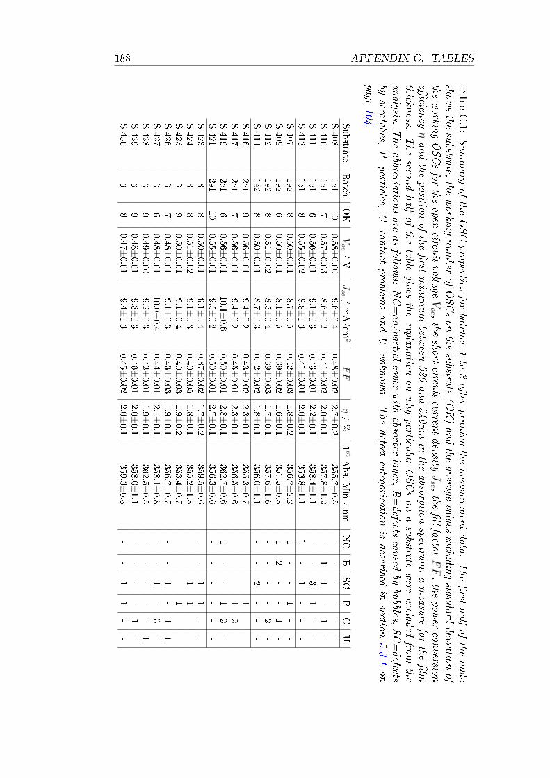
188 APPENDIX C. TABLES
Table
C.1:
Summary
ofthe
OSCproperties
forbatches
1to
3after
pruningthe
measu
rementdata.
The
rst
halfof
thetable
showsthe
substrate,
theworkin
gnumber
ofOSCson
thesubstrate
(OK)andthe
averagevalu
esinclu
dingstan
darddeviation
ofthe
workin
gOSCsfor
theopen
circuitvoltage
Voc ,the
shortcircu
itcurren
tden
sityJ
sc ,the
llfactor
FF,the
power
conversion
ecien
cyηandthe
positionof
therst
minim
um
between
320and540n
min
theabsorption
spectrum,ameasu
refor
thelm
thickness.
The
secondhalf
ofthe
tablegives
theexplan
ationon
why
particular
OSCson
asubstrate
were
excluded
fromthe
analysis.
The
abbreviationsare
asfollow
s:NC=no/partial
coverwith
absorberlayer,
B=defects
caused
bybubbles,
SC=defects
byscratches,
P=particles,
C=con
tactproblem
sandU=unknow
n.The
defectcategorisation
isdescribed
insection
5.3.1on
page104.S
ubstrate
Batch
OK
Voc/V
Jsc/mA/cm
2F
Fη/%
1stAbs.Min
/nm
NC
BSC
PC
US408
1e110
0.58±0.00
9.6±0.4
0.48±0.02
2.7±0.2
355.7±0.5
--
--
--
S410
1e17
0.57±0.03
8.6±0.2
0.41±0.02
2.0±0.1
357.8±1.2
-1
1-
1-
S411
1e16
0.56±0.01
9.1±0.3
0.43±0.01
2.2±0.1
358.4±1.1
--
31
--
S413
1e18
0.55±0.02
8.8±0.3
0.41±0.04
2.0±0.1
353.8±1.1
1-
1-
--
S407
1e28
0.50±0.01
8.7±0.5
0.42±0.03
1.8±0.2
356.7±2.2
1-
-1
--
S409
1e26
0.50±0.01
8.1±0.5
0.39±0.02
1.6±0.1
357.5±0.8
12
--
1-
S412
1e28
0.51±0.02
8.5±0.4
0.39±0.03
1.7±0.1
357.6±1.6
--
--
2-
S414
1e28
0.50±0.01
8.7±0.3
0.42±0.02
1.8±0.1
356.0±1.1
--
2-
--
S416
2e19
0.56±0.01
9.4±0.2
0.43±0.02
2.3±0.1
355.3±0.7
--
-1
--
S417
2e17
0.56±0.01
9.4±0.2
0.45±0.01
2.3±0.1
356.5±0.6
--
-1
2-
S419
2e16
0.56±0.01
10.1±0.6
0.50±0.01
2.8±0.1
362.7±0.6
1-
-1
2-
S421
2e110
0.55±0.01
9.5±0.2
0.50±0.01
2.7±0.1
356.3±0.6
--
--
--
S423
38
0.50±0.01
9.1±0.4
0.37±0.02
1.7±0.2
359.5±0.6
--
11
--
S424
38
0.51±0.02
9.1±0.3
0.40±0.05
1.8±0.1
355.2±1.8
--
11
--
S425
39
0.50±0.01
9.1±0.4
0.40±0.03
1.9±0.2
353.4±0.7
--
-1
--
S426
37
0.48±0.01
9.1±0.3
0.43±0.03
1.9±0.1
356.7±0.7
--
1-
11
S427
36
0.48±0.01
10.0±0.4
0.44±0.01
2.1±0.1
358.1±0.8
--
1-
3-
S428
39
0.49±0.00
9.2±0.3
0.42±0.01
1.9±0.1
362.5±0.5
--
--
-1
S429
39
0.48±0.01
9.3±0.3
0.46±0.01
2.0±0.1
358.0±1.1
--
--
1-
S430
38
0.47±0.01
9.4±0.3
0.45±0.02
2.0±0.1
359.3±0.8
--
11
--
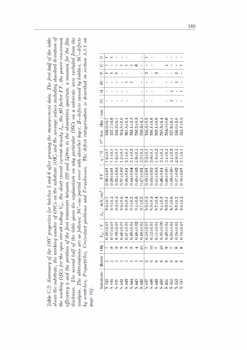
189
TableC.2:Summaryof
theOSCproperties
forbatches5and6afterpruningthemeasurementdata.The
rsthalfof
thetable
show
sthesubstrate,theworkingnumberof
OSCson
thesubstrate(O
K)andtheaveragevalues
includingstandard
deviationof
theworkingOSCsfortheopen
circuitvoltage
Voc,theshortcircuitcurrentdensity
Jsc,thellfactor
FF,thepower
conversion
eciency
ηandtheposition
oftherstminim
um
between320and540nm
intheabsorption
spectrum,ameasure
forthelm
thickness.
The
secondhalfof
thetablegivestheexplanationon
why
particularOSCson
asubstratewereexcludedfrom
the
analysis.The
abbreviationsareas
follow
s:NC=no/partialcoverwithabsorber
layer,B=defectscausedby
bubbles,SC=defects
byscratches,
P=particles,
C=contact
problemsandU=unknow
n.The
defect
categorisation
isdescribedin
section5.3.1on
page
104. Substrate
Batch
OK
Voc/V
Jsc/mA/cm
2F
Fη/%
1stAbs.Min
/nm
NC
BSC
PC
US439
57
0.50±0.01
9.0±
0.2
0.36±0.01
1.6±
0.1
356.0±
0.7
--
-1
11
S440
58
0.47±0.01
8.4±
0.3
0.29±0.01
1.1±
0.1
357.7±
0.9
--
-1
-1
S441
59
0.49±0.01
9.0±
0.3
0.35±0.03
1.6±
0.1
356.2±
0.7
--
-1
--
S442
59
0.46±0.01
8.6±
0.6
0.31±0.02
1.2±
0.1
354.8±
1.0
--
--
1-
S443
58
0.47±0.01
9.9±
0.4
0.45±0.01
2.1±
0.1
361.5±
1.4
--
1-
1-
S444
58
0.49±0.01
9.5±
0.2
0.44±0.04
2.1±
0.2
356.1±
1.2
--
1-
1-
S445
54
0.48±0.02
9.1±
0.6
0.45±0.03
1.9±
0.1
356.2±
0.3
--
--
6-
S446
510
0.48±0.01
9.7±
0.2
0.47±0.01
2.2±
0.1
359.3±
1.1
--
--
--
S447
67
0.54±0.01
8.9±
0.3
0.48±0.01
2.3±
0.1
356.3±
1.5
--
-2
-1
S448
610
0.52±0.01
8.9±
0.3
0.43±0.02
2.0±
0.1
356.1±
0.9
--
--
--
S449
67
0.51±0.01
8.7±
0.4
0.41±0.03
1.8±
0.2
353.1±
0.9
--
-3
--
S450
610
0.50±0.00
9.1±
0.3
0.46±0.01
2.1±
0.1
355.3±
1.4
--
--
--
S451
69
0.49±0.01
8.9±
0.5
0.48±0.00
2.1±
0.1
354.0±
0.6
--
--
1-
S452
67
0.50±0.01
8.7±
0.6
0.49±0.00
2.1±
0.2
357.6±
1.1
21
--
--
S453
68
0.48±0.01
8.8±
0.2
0.47±0.02
2.0±
0.1
356.0±
1.0
--
11
--
S454
68
0.48±0.01
9.0±
0.3
0.48±0.01
2.1±
0.1
355.1±
1.8
-1
--
1-
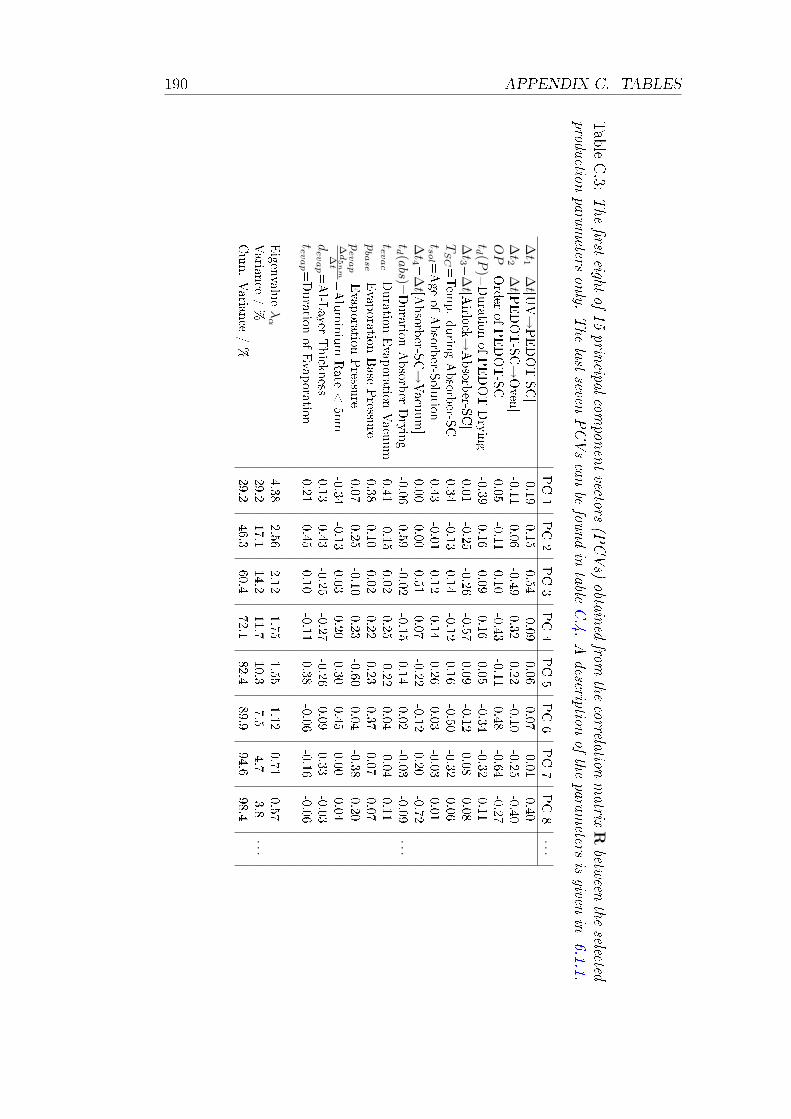
190 APPENDIX C. TABLES
Table
C.3:
The
rst
eightof
15prin
cipalcom
ponentvectors
(PCVs)
obtained
fromthe
correlationmatrix
Rbetw
eenthe
selectedprodu
ctionparam
etersonly.
The
lastseven
PCVscan
befou
ndin
tableC.4.
Adescription
ofthe
parameters
isgiven
in6.1.1.
PC1
PC2
PC3
PC4
PC5
PC6
PC7
PC8
···∆
t1 =
∆t[U
V→PEDOT-SC]
-0.190.15
0.54-0.09
0.060.07
-0.010.40
∆t2 =
∆t[P
EDOT-SC→Oven
]-0.11
0.06-0.49
0.320.22
-0.10-0.25
-0.40O
P=Order
ofPEDOT-SC
0.05-0.11
0.10-0.43
-0.110.48
-0.64-0.27
td (P
)=Duration
ofPEDOTDrying
-0.390.16
0.090.16
0.05-0.34
-0.320.11
∆t3 =
∆t[A
irlock→
Absorb
er-SC]
0.01-0.25
-0.26-0.57
0.09-0.12
0.080.08
TS
C=Tem
p.durin
gAbsorb
er-SC
0.34-0.13
0.14-0.12
0.16-0.50
-0.320.06
tsol =Age
ofAbsorb
er-Solu
tion0.43
-0.010.12
0.140.26
0.03-0.03
0.01∆
t4 =
∆t[A
bsorb
er-SC→Vacu
um]
0.000.00
0.510.07
-0.22-0.12
0.20-0.72
td (a
bs)=Duration
Absorb
erDrying
-0.060.59
-0.02-0.15
0.140.02
-0.03-0.09
···tevac =
Duration
Evap
orationVacu
um
0.41-0.15
0.020.25
-0.220.04
-0.040.11
pbase =
Evaporation
Base
Pressu
re0.38
0.100.02
0.220.23
0.370.07
0.07p
evap =
Evaporation
Pressu
re0.07
0.25-0.10
0.23-0.60
0.04-0.38
0.20∆
d5
nm
∆t
=Aluminium
Rate
<5nm
-0.34-0.13
0.030.20
0.300.45
0.000.04
devap =
Al-L
ayerThick
ness
0.130.43
-0.25-0.27
-0.260.09
0.33-0.03
tevap =
Duration
ofEvap
oration0.21
0.450.10
-0.110.38
-0.06-0.16
-0.06
Eigen
value
λα
4.382.56
2.121.75
1.551.12
0.710.57
Varian
ce/%
29.217.1
14.211.7
10.37.5
4.73.8
···Cum.Varian
ce/%
29.246.3
60.472.1
82.489.9
94.698.4
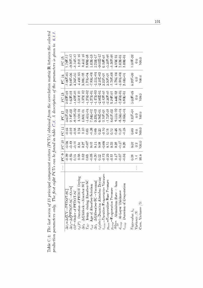
191
TableC.4:The
lastsevenof
15principalcomponentvectors(PCVs)
obtained
from
thecorrelationmatrixR
betweentheselected
productionparametersonly.The
rsteightPCVscanbe
foundin
tableC.3.Adescriptionof
theparametersisgivenin
6.1.1.
···
PC9
PC10
PC11
PC12
PC13
PC14
PC15
∆t 1=
∆t[UV→PEDOT-SC]
-0.39
-0.56
-0.03
3.65E-02
2.07E-02
-1.06E
-05
1.78E-17
∆t 2=
∆t[PEDOT-SC→Oven]
-0.35
-0.49
-0.02
2.14E-02
1.65E-02
9.04E-06
-9.20E
-17
OP=Order
ofPEDOT-SC
0.13
-0.11
-0.08
-9.12E
-02
-1.63E
-01
4.76E-05
-1.74E
-17
t d(P
)=Duration
ofPEDOTDrying
-0.08
0.31
-0.24
-3.10E
-01
-5.51E
-01
-4.43E
-05
-1.21E
-16
∆t 3=
∆t[Airlock→Absorber-SC]
-0.62
0.27
-0.10
1.80E-01
-5.37E
-02
3.09E-03
-8.41E
-16
TS
C=Tem
p.duringAbsorber-SC
0.03
-0.07
0.65
-1.41E
-01
-1.25E
-02
1.70E-04
8.68E-16
t sol=Age
ofAbsorber-Solution
-0.05
0.03
-0.26
7.34E-02
-1.27E
-01
-7.83E
-01
1.12E-13
∆t 4=
∆t[Absorber-SC→Vacuum]
-0.30
0.14
0.06
3.23E-03
-1.47E
-03
-1.21E
-04
2.21E-17
t d(a
bs)=
Duration
Absorber
Drying
···
0.12
0.08
0.25
6.56E-01
-2.86E
-01
-2.10E
-03
-9.03E
-17
t evac=Duration
EvaporationVacuum
-0.12
-0.06
-0.10
2.10E-01
-3.43E
-01
3.25E-01
6.20E-01
pbase=EvaporationBasePressure
-0.25
0.15
0.11
-1.73E
-01
-2.36E
-01
3.50E-01
-5.39E
-01
pevap=EvaporationPressure
-0.31
0.23
0.12
8.65E-02
3.28E-01
-1.78E
-01
-1.20E
-01
∆d5
nm
∆t
=Aluminium
Rate<5nm
-0.17
0.28
0.46
-9.11E
-02
5.44E-02
-1.78E
-01
4.05E-01
devap=Al-Layer
Thickness
-0.07
-0.17
0.18
-5.24E
-01
-2.35E
-01
-1.90E
-01
2.12E-01
t evap=Duration
ofEvaporation
-0.04
0.20
-0.28
-2.03E
-01
4.80E-01
2.44E-01
3.19E-01
Eigenvalue
λα
0.21
0.02
0.00
1.25E-04
5.62E-05
8.92E-09
1.01E-32
Variance
/%···
1.4
0.2
0.0
0.0
0.0
0.0
0.0
Cum.Variance
/%99.8
100.0
100.0
100.0
100.0
100.0
100.0
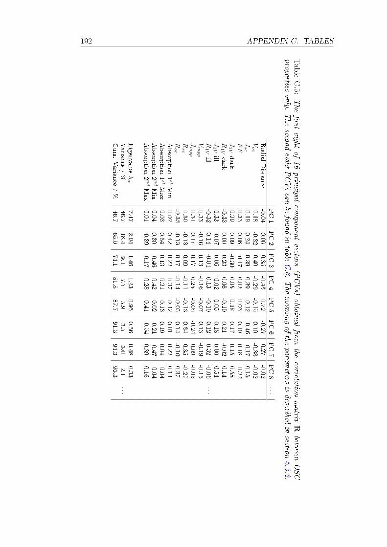
192 APPENDIX C. TABLES
Table
C.5:
The
rst
eightof
16prin
cipalcom
ponentvectors
(PCVs)
obtained
fromthe
correlationmatrix
Rbetw
eenOSC
propertiesonly.
The
secondeight
PCVscan
befou
ndin
tableC.6.
The
mean
ingof
theparam
etersisdescribed
insection
5.3.2.
PC1
PC2
PC3
PC4
PC5
PC6
PC7
PC8
···Radial
Distan
ce-0.04
0.060.35
-0.430.72
-0.270.27
-0.02V
oc
0.18-0.32
0.40-0.29
-0.150.10
-0.38-0.02
Jsc
0.190.24
0.390.39
-0.12-0.46
-0.170.15
FF
0.350.06
-0.170.02
0.050.10
0.18-0.22
J1Vdark
0.290.09
-0.300.05
0.180.17
0.150.58
R1Vdark
-0.330.00
0.230.06
-0.100.21
-0.020.14
J1Vill
0.33-0.07
0.06-0.02
0.050.18
0.000.54
R1Vill
-0.320.14
-0.040.13
-0.100.12
0.32-0.06
···V
mpp
0.33-0.16
0.13-0.16
-0.070.13
-0.19-0.15
Jm
pp
0.310.17
0.170.25
-0.05-0.24
0.09-0.05
Rsc
0.30-0.13
0.09-0.11
-0.130.34
0.35-0.27
Roc
-0.33-0.13
0.17-0.14
-0.050.14
-0.100.37
Absorp
tion1
stMin
0.020.42
0.22-0.37
-0.420.01
0.220.14
Absorp
tion1
stMax
0.030.54
0.13-0.21
-0.130.19
0.04-0.04
Absorp
tion2
ndMin
0.040.30
-0.46-0.42
-0.02-0.21
-0.47-0.04
Absorp
tion2
ndMax
0.01-0.39
-0.17-0.28
-0.41-0.54
0.390.16
Eigen
value
λα
7.472.94
1.461.23
0.950.56
0.480.33
Varian
ce/%
46.718.4
9.17.7
5.93.5
3.02.1
···Cum.Varian
ce/%
46.765.0
74.181.8
87.791.3
94.396.3
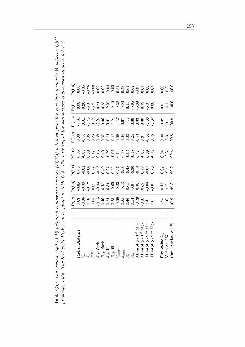
193
TableC.6:The
secondeightof
16principalcomponentvectors(PCVs)
obtained
from
thecorrelationmatrix
RbetweenOSC
properties
only.The
rsteightPCVscanbe
foundin
tableC.5.The
meaningof
theparametersisdescribedin
section5.3.2.
···
PC9
PC10
PC11
PC12
PC13
PC14
PC15
PC16
RadialDistance
0.09
-0.05
0.05
0.05
0.00
-0.04
0.00
0.00
Voc
-0.06
-0.39
-0.01
-0.05
-0.06
0.31
0.26
-0.35
Jsc
0.16
-0.12
-0.08
0.00
0.08
-0.45
-0.04
-0.26
FF
0.05
0.02
0.27
0.17
0.23
0.17
-0.47
-0.58
J1Vdark
-0.13
-0.43
-0.12
0.16
0.32
-0.04
0.24
0.02
R1Vdark
0.46
0.15
0.40
0.40
0.37
0.06
0.25
0.02
J1Vill
0.24
0.34
0.27
-0.20
-0.51
0.01
-0.07
-0.04
R1Vill
···
0.23
-0.65
0.22
-0.07
-0.43
-0.04
-0.10
-0.05
Vm
pp
-0.09
-0.23
0.37
0.14
0.09
-0.37
-0.32
0.54
Jm
pp
0.25
-0.10
-0.10
0.00
0.04
0.67
-0.09
0.43
Rsc
0.46
0.05
-0.48
-0.04
0.03
-0.27
0.15
0.01
Roc
0.14
-0.07
-0.36
-0.17
0.24
0.06
-0.65
0.02
Absorption
1stMin
-0.29
0.10
-0.14
0.47
-0.21
0.03
-0.08
-0.01
Absorption
1stMax
-0.07
0.02
0.22
-0.65
0.31
0.00
0.12
0.01
Absorption
2n
dMin
0.47
-0.08
-0.07
0.09
-0.08
-0.03
-0.01
0.00
Absorption
2n
dMax
0.07
-0.01
0.20
-0.18
0.18
-0.02
0.06
0.01
Eigenvalue
λα
0.25
0.13
0.07
0.04
0.04
0.02
0.01
0.00
Variance
/%
···
1.6
0.8
0.5
0.3
0.3
0.1
0.1
0.0
Cum.Variance
/%
97.9
98.8
99.2
99.5
99.8
99.9
100.0
100.0
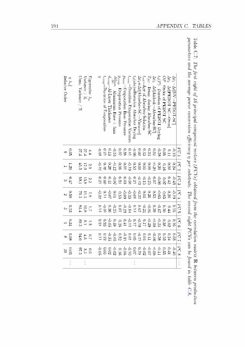
194 APPENDIX C. TABLES
Table
C.7:
The
rst
eightof
16prin
cipalcom
ponentvectors
(PCVs)
obtained
fromthe
correlationmatrix
Rbetw
eenprodu
ctionparam
etersandthe
averagepow
ercon
versione
ciency
ηper
substrate.
The
secondeight
PCVscan
befou
ndin
tableC.8.
PC1
PC2
PC3
PC4
PC5
PC6
PC7
PC8
···∆
t1 =
∆t[U
V→PEDOT-SC]
-0.190.24
-0.43-0.19
0.150.16
0.03-0.40
∆t2 =
∆t[P
EDOT-SC→Oven
]-0.11
0.000.42
0.20-0.44
-0.020.24
0.41O
P=Order
ofPEDOT-SC
0.05-0.16
-0.07-0.03
0.500.38
0.530.33
td (P
)=Duration
ofPEDOTDrying
-0.380.20
-0.06-0.05
-0.17-0.21
0.38-0.11
∆t3 =
∆t[A
irlock→
Absorb
er-SC]
0.01-0.20
0.070.53
0.39-0.08
-0.06-0.08
TS
C=Tem
p.durin
gAbsorb
er-SC
0.340.00
-0.250.26
-0.01-0.29
0.41-0.07
tsol =Age
ofAbsorb
er-Solu
tion0.43
0.05-0.15
0.05-0.21
0.170.04
-0.02∆
t4 =
∆t[A
bsorb
er-SC→Vacu
um]
0.000.09
-0.43-0.32
0.07-0.19
-0.210.70
td (a
bs)=Duration
Absorb
erDrying
-0.060.53
0.21-0.01
0.140.17
0.050.07
···tevac =
Duration
Evap
orationVacu
um
0.41-0.19
-0.01-0.23
-0.14-0.11
0.01-0.10
pbase =
Evaporation
Base
Pressu
re0.38
0.070.03
-0.09-0.23
0.41-0.11
-0.05p
evap =
Evaporation
Pressu
re0.07
0.060.31
-0.530.07
-0.250.32
-0.16∆
d5
nm
∆t
=Aluminium
Rate
<5nm
-0.34-0.12
-0.070.01
-0.250.49
-0.05-0.02
devap =
Al-L
ayerThick
ness
0.130.28
0.41-0.07
0.36-0.05
-0.350.02
tevap =
Duration
ofEvap
oration0.21
0.480.00
0.14-0.01
0.230.22
0.05η
-0.01-0.42
0.21-0.32
0.140.24
0.11-0.05
Eigen
value
λα
4.42.9
2.21.8
1.71.3
0.70.6
Varian
ce/%
27.417.9
13.811.5
10.88.1
4.53.5
···Cum.Varian
ce/%
27.445.3
59.170.5
81.489.5
94.097.5
|ηλ
α|
0.051.20
0.470.59
0.230.31
0.080.03
···Relative
Order
91
32
54
810
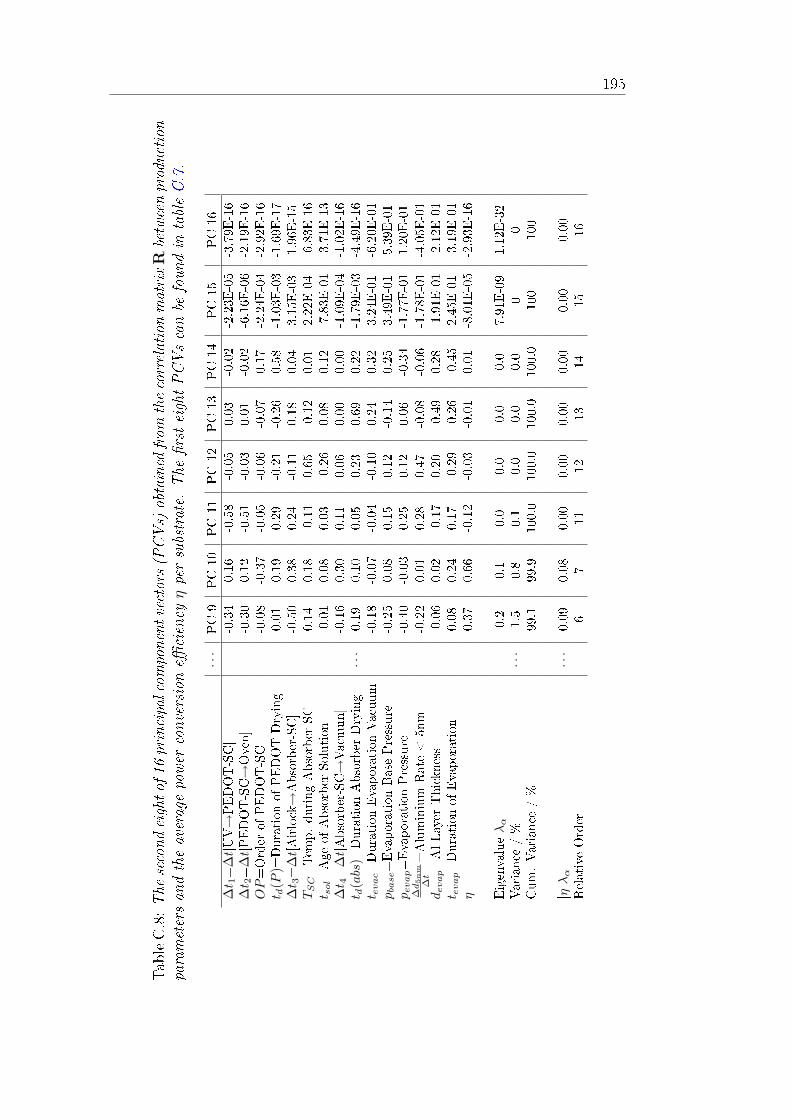
195
TableC.8:The
secondeightof16
principalcomponentvectors(PCVs)obtained
from
thecorrelationmatrixR
betweenproduction
parametersandtheaveragepower
conversione
ciency
ηpersubstrate.
The
rsteightPCVscanbe
foundin
tableC.7.
···
PC9
PC10
PC11
PC12
PC13
PC14
PC15
PC16
∆t 1=
∆t[UV→PEDOT-SC]
-0.34
0.16
-0.58
-0.05
0.03
-0.02
-2.23E
-05
-3.79E
-16
∆t 2=
∆t[PEDOT-SC→Oven]
-0.30
0.12
-0.51
-0.03
0.01
-0.02
-6.16E
-06
-2.19E
-16
OP=Order
ofPEDOT-SC
-0.08
-0.37
-0.05
-0.06
-0.07
0.17
-2.24E
-04
-2.92E
-16
t d(P
)=Duration
ofPEDOTDrying
0.01
0.19
0.29
-0.21
-0.26
0.58
-1.03E
-03
-1.69E
-17
∆t 3=
∆t[Airlock→Absorber-SC]
-0.50
0.38
0.24
-0.11
0.18
0.04
3.15E-03
1.96E-15
TS
C=Tem
p.duringAbsorber-SC
0.14
0.18
-0.11
0.65
-0.12
0.01
2.22E-04
-6.83E
-16
t sol=Age
ofAbsorber-Solution
-0.01
0.08
0.03
-0.26
0.08
0.12
-7.83E
-01
-3.71E
-13
∆t 4=
∆t[Absorber-SC→Vacuum]
-0.16
0.30
0.11
0.06
0.00
0.00
-1.09E
-04
-1.02E
-16
t d(a
bs)=
Duration
Absorber
Drying
···
0.19
0.10
0.05
0.23
0.69
0.22
-1.79E
-03
-4.49E
-16
t evac=Duration
EvaporationVacuum
-0.18
-0.07
-0.04
-0.10
0.24
0.32
3.24E-01
-6.20E
-01
pbase=EvaporationBasePressure
-0.25
0.08
0.15
0.12
-0.14
0.25
3.49E-01
5.39E-01
pevap=EvaporationPressure
-0.40
-0.03
0.25
0.12
0.06
-0.34
-1.77E
-01
1.20E-01
∆d5
nm
∆t
=Aluminium
Rate<5nm
-0.22
0.01
0.28
0.47
-0.08
-0.06
-1.78E
-01
-4.05E
-01
devap=Al-Layer
Thickness
-0.06
0.02
-0.17
0.20
-0.49
0.28
-1.91E
-01
-2.12E
-01
t evap=Duration
ofEvaporation
0.08
0.24
0.17
-0.29
-0.26
-0.45
2.45E-01
-3.19E
-01
η0.37
0.66
-0.12
-0.03
-0.01
0.01
-8.01E
-05
-2.93E
-16
Eigenvalue
λα
0.2
0.1
0.0
0.0
0.0
0.0
7.91E-09
1.12E-32
Variance
/%
···
1.5
0.8
0.1
0.0
0.0
0.0
00
Cum.Variance
/%
99.1
99.9
100.0
100.0
100.0
100.0
100
100
|ηλ
α|
···
0.09
0.08
0.00
0.00
0.00
0.00
0.00
0.00
RelativeOrder
67
1112
1314
1516
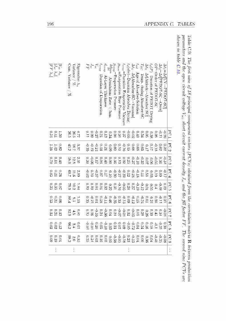
196 APPENDIX C. TABLES
Table
C.9:
The
rst
nineof
18prin
cipalcom
ponentvectors
(PCVs)
obtained
fromthe
correlationmatrix
Rbetw
eenprodu
ctionparam
etersandthe
opencircu
itvoltage
Voc ,short
circuitcurren
tden
sityJ
scandthe
llfactor
FF.The
secondninePCVsare
shownin
tableC.10.
PC1
PC2
PC3
PC4
PC5
PC6
PC7
PC8
PC9
···∆
t1 =
∆t[U
V→PEDOT-SC]
-0.200.22
-0.34-0.17
0.290.21
-0.040.38
-0.08∆
t2 =
∆t[P
EDOT-SC→Oven
]-0.11
0.020.36
0.09-0.48
-0.110.34
-0.31-0.25
OP=Order
ofPEDOT-SC
0.08-0.18
-0.050.19
0.40.38
0.45-0.1
-0.41td (P
)=Duration
ofPEDOTDrying
-0.380.17
-0.06-0.03
-0.05-0.21
0.390.18
0.04∆
t3 =
∆t[A
irlock→
Absorb
er-SC]
0.05-0.17
-0.070.58
-0.010.01
-0.260.16
-0.36T
SC=Tem
p.durin
gAbsorb
er-SC
0.340.03
-0.320.11
-0.12-0.21
0.280.24
0.00tsol =Age
ofAbsorb
er-Solu
tion0.40
0.08-0.10
-0.18-0.19
0.150.05
0.040.04
∆t4 =
∆t[A
bsorb
er-SC→Vacu
um]
-0.020.08
-0.37-0.28
0.27-0.12
-0.03-0.72
-0.13td (a
bs)=Duration
Absorb
erDrying
-0.050.45
0.250.12
0.200.09
0.12-0.05
0.23···
tevac =
Duration
Evap
orationVacu
um
0.37-0.16
0.02-0.32
-0.05-0.13
-0.040.09
-0.18p
base =
Evaporation
Base
Pressu
re0.34
0.100.13
-0.27-0.16
0.33-0.07
0.02-0.05
pevap =
Evaporation
Pressu
re0.04
0.000.36
-0.300.31
-0.350.24
0.23-0.38
∆d5
nm
∆t
=Aluminium
Rate
<5nm
-0.34-0.09
0.00-0.10
-0.220.46
0.04-0.03
-0.05d
evap =
Al-L
ayerThick
ness
0.130.21
0.400.17
0.33-0.11
-0.36-0.10
0.03tevap =
Duration
ofEvap
oration0.21
0.440.04
0.070.01
0.180.24
0.050.16
Voc
-0.27-0.24
0.17-0.37
0.040.04
-0.160.20
0.03J
sc
0.09-0.42
-0.060.10
0.19-0.21
0.26-0.04
0.54F
F0.11
-0.350.30
-0.020.19
0.350.15
-0.040.25
Eigen
value
λα
4.773.37
2.312.09
1.841.53
0.810.61
0.35Varian
ce/%
26.518.7
12.811.6
10.28.5
4.53.4
2.0···
Cum.Varian
ce/%
26.545.2
58.069.7
79.988.4
92.996.2
98.2
|Voc
λα|
1.300.82
0.400.76
0.070.06
0.130.12
0.01|J
sc
λα|
0.411.42
0.140.21
0.350.31
0.210.02
0.19···
|FF
λα|
0.541.16
0.700.05
0.350.53
0.120.02
0.09
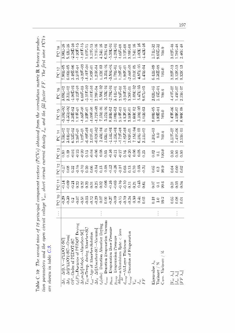
197
TableC.10:
The
secondnineof
18principalcomponentvectors(PCVs)
obtained
from
thecorrelationmatrix
Rbetweenproduc-
tion
parametersandtheopen
circuitvoltage
Voc,shortcircuitcurrentdensity
Jscandthellfactor
FF.The
rstninePCVs
areshow
nin
tableC.9.
···
PC10
PC11
PC12
PC13
PC14
PC15
PC16
PC17
PC18
∆t 1=
∆t[UV→PEDOT-SC]
-0.29
-0.14
-0.17
0.60
5.73E-02
-3.10E
-02
3.69E-02
7.90E-05
3.96E-16
∆t 2=
∆t[PEDOT-SC→Oven]
-0.30
-0.09
0.08
0.49
3.64E-02
-1.35E
-02
2.31E-02
6.06E-05
5.42E-16
OP=Order
ofPEDOT-SC
0.2
-0.21
0.32
-0.04
6.53E-02
3.59E-02
-1.90E
-01
3.48E-06
-2.38E
-16
t d(P
)=Duration
ofPEDOTDrying
-0.07
0.23
-0.18
-0.23
2.28E-01
1.11E-01
-6.23E
-01
3.51E-04
-1.93E
-15
∆t 3=
∆t[Airlock→Absorber-SC]
-0.51
0.22
-0.10
-0.20
1.02E-01
-1.86E
-01
6.68E-03
-3.29E
-03
-1.81E
-15
TS
C=Tem
p.duringAbsorber-SC
-0.03
0.29
0.20
0.13
-6.49E
-01
1.33E-01
-5.31E
-02
-1.41E
-04
1.01E-15
t sol=Age
ofAbsorber-Solution
-0.12
0.01
0.06
-0.04
2.61E-01
-1.09E
-01
-1.01E
-01
7.83E-01
3.57E-13
∆t 4=
∆t[Absorber-SC→Vacuum]
-0.29
0.25
-0.04
-0.06
-6.02E
-02
-1.72E
-03
2.79E-04
1.25E-04
1.71E-16
t d(a
bs)=
Duration
Absorber
Drying
···
-0.07
0.02
0.13
-0.08
-2.43E
-01
-7.13E
-01
-5.38E
-02
1.12E-03
4.24E-16
t evac=Duration
EvaporationVacuum
0.00
-0.06
-0.08
0.05
1.03E-01
-3.12E
-01
-2.53E
-01
-3.25E
-01
6.20E-01
pbase=EvaporationBasePressure
-0.27
-0.16
-0.12
-0.16
-1.14E
-01
8.16E-02
-2.79E
-01
-3.50E
-01
-5.39E
-01
pevap=EvaporationPressure
-0.09
-0.03
-0.26
-0.21
-1.23E
-01
2.08E-02
3.44E-01
1.78E-01
-1.20E
-01
∆d5
nm
∆t
=Aluminium
Rate<5nm
-0.15
-0.16
-0.24
-0.27
-4.72E
-01
9.54E-02
2.83E-02
1.78E-01
4.05E-01
devap=Al-Layer
Thickness
-0.10
-0.10
0.03
0.16
-1.85E
-01
4.15E-01
-3.94E
-01
1.90E-01
2.12E-01
t evap=Duration
ofEvaporation
-0.24
0.11
0.13
-0.20
2.83E-01
3.56E-01
3.76E-01
-2.44E
-01
3.19E-01
Voc
-0.30
0.21
0.70
-0.06
-7.15E
-04
1.66E-02
-1.69E
-02
5.01E-05
1.74E-16
Jsc
-0.41
-0.43
-0.05
-0.05
6.18E-03
-5.10E
-03
-5.47E
-03
-4.87E
-05
-1.02E
-16
FF
0.03
0.61
-0.31
0.25
2.11E-02
1.01E-03
9.67E-03
1.45E-04
-1.42E
-16
Eigenvalue
λα
0.18
0.07
0.05
0.02
1.20E-03
8.88E-05
2.62E-05
6.42E-09
1.74E-32
Variance
/%
···
1.0
0.4
0.3
0.1
0.0
4.93E-04
1.45E-04
3.56E-08
9.65E-32
Cum.Variance
/%
99.2
99.6
99.9
100.0
100.0
100.0
100.0
100.0
100.0
|Voc
λα|
0.05
0.01
0.04
0.00
8.57E-07
1.47E-06
4.41E-07
3.22E-13
3.02E-48
|Jsc
λα|
···
0.08
0.03
0.00
0.00
7.41E-06
4.53E-07
1.43E-07
3.12E-13
1.78E-48
|FF
λα|
0.01
0.04
0.02
0.00
2.53E-05
8.98E-08
2.53E-07
9.32E-13
2.46E-48
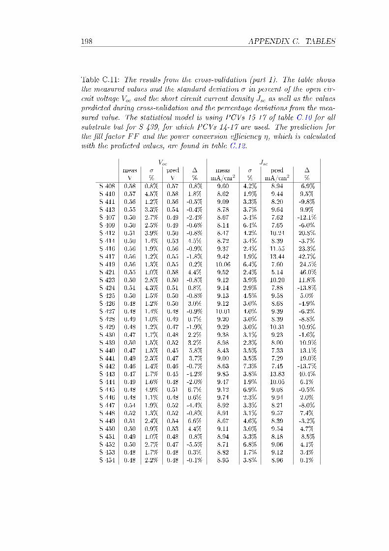
198 APPENDIX C. TABLES
Table C.11: The results from the cross-validation (part 1). The table showsthe measured values and the standard deviation σ in percent of the open cir-cuit voltage Voc and the short circuit current density Jsc as well as the valuespredicted during cross-validation and the percentage deviations from the mea-sured value. The statistical model is using PCVs 15-17 of table C.10 for allsubstrate but for S 439, for which PCVs 14-17 are used. The prediction forthe ll factor FF and the power conversion eciency η, which is calculatedwith the predicted values, are found in table C.12.
Voc Jsc
meas σ pred ∆ meas σ pred ∆V % V % mA/cm2 % mA/cm2 %
S 408 0.58 0.8% 0.57 -0.8% 9.60 4.2% 8.94 -6.9%S 410 0.57 4.5% 0.58 1.8% 8.62 1.9% 9.44 9.5%S 411 0.56 1.2% 0.56 -0.5% 9.09 3.3% 8.20 -9.8%S 413 0.55 3.3% 0.54 -0.4% 8.78 3.7% 9.64 9.9%S 407 0.50 2.7% 0.49 -2.4% 8.67 5.4% 7.62 -12.1%S 409 0.50 2.5% 0.49 -0.6% 8.14 6.4% 7.65 -6.0%S 412 0.51 3.9% 0.50 -0.8% 8.47 4.2% 10.24 20.8%S 414 0.50 1.4% 0.53 4.5% 8.72 3.4% 8.39 -3.7%S 416 0.56 1.9% 0.56 -0.9% 9.37 2.4% 11.55 23.3%S 417 0.56 1.2% 0.55 -1.8% 9.42 1.9% 13.44 42.7%S 419 0.56 1.3% 0.55 -0.2% 10.06 6.4% 7.60 -24.5%S 421 0.55 1.0% 0.58 4.4% 9.52 2.4% 5.14 -46.0%S 423 0.50 2.8% 0.50 -0.8% 9.12 3.9% 10.20 11.8%S 424 0.51 4.3% 0.51 0.8% 9.14 2.9% 7.88 -13.8%S 425 0.50 1.5% 0.50 -0.8% 9.13 4.5% 9.58 5.0%S 426 0.48 1.2% 0.50 3.0% 9.12 3.0% 8.68 -4.9%S 427 0.48 1.4% 0.48 -0.9% 10.01 4.0% 9.39 -6.2%S 428 0.49 1.0% 0.49 0.7% 9.20 3.0% 8.39 -8.8%S 429 0.48 1.2% 0.47 -1.9% 9.29 3.0% 10.31 10.9%S 430 0.47 1.7% 0.48 2.2% 9.38 3.1% 9.23 -1.6%S 439 0.50 1.5% 0.52 3.2% 8.98 2.3% 8.00 -10.9%S 440 0.47 1.5% 0.45 -5.8% 8.43 3.5% 7.33 -13.1%S 441 0.49 2.3% 0.47 -3.7% 9.00 3.5% 7.29 -19.0%S 442 0.46 1.4% 0.46 -0.7% 8.63 7.3% 7.45 -13.7%S 443 0.47 1.7% 0.45 -4.2% 9.85 3.8% 13.83 40.4%S 444 0.49 1.6% 0.48 -2.0% 9.47 1.9% 10.05 6.1%S 445 0.48 4.9% 0.51 6.7% 9.12 6.9% 9.08 -0.5%S 446 0.48 1.1% 0.48 0.6% 9.74 2.3% 9.94 2.0%S 447 0.54 1.9% 0.52 -4.4% 8.92 3.3% 8.21 -8.0%S 448 0.52 1.3% 0.52 -0.8% 8.91 3.1% 9.57 7.4%S 449 0.51 2.4% 0.54 6.6% 8.67 4.6% 8.39 -3.2%S 450 0.50 0.9% 0.53 4.4% 9.11 3.0% 9.54 4.7%S 451 0.49 1.0% 0.48 -0.8% 8.94 5.3% 8.18 -8.5%S 452 0.50 2.7% 0.47 -5.5% 8.71 6.8% 9.06 4.1%S 453 0.48 1.7% 0.48 0.3% 8.82 1.7% 9.12 3.4%S 454 0.48 2.2% 0.48 -0.1% 8.95 3.8% 8.96 0.1%
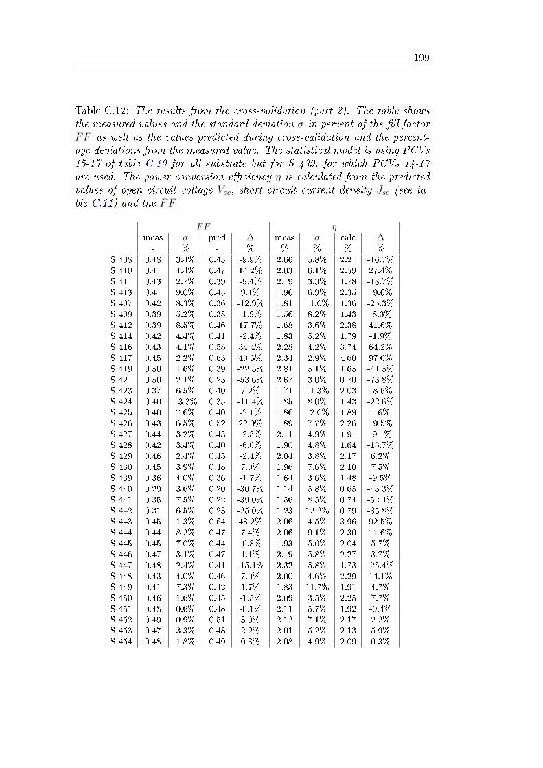
199
Table C.12: The results from the cross-validation (part 2). The table showsthe measured values and the standard deviation σ in percent of the ll factorFF as well as the values predicted during cross-validation and the percent-age deviations from the measured value. The statistical model is using PCVs15-17 of table C.10 for all substrate but for S 439, for which PCVs 14-17are used. The power conversion eciency η is calculated from the predictedvalues of open circuit voltage Voc, short circuit current density Jsc (see ta-ble C.11) and the FF .
FF ηmeas σ pred ∆ meas σ calc ∆- % - % % % % %
S 408 0.48 3.4% 0.43 -9.9% 2.66 5.8% 2.21 -16.7%S 410 0.41 4.4% 0.47 14.2% 2.03 6.1% 2.59 27.4%S 411 0.43 2.7% 0.39 -9.4% 2.19 3.3% 1.78 -18.7%S 413 0.41 9.0% 0.45 9.1% 1.96 6.9% 2.35 19.6%S 407 0.42 8.3% 0.36 -12.9% 1.81 11.0% 1.36 -25.3%S 409 0.39 5.2% 0.38 -1.9% 1.56 8.2% 1.43 -8.3%S 412 0.39 8.5% 0.46 17.7% 1.68 3.6% 2.38 41.6%S 414 0.42 4.4% 0.41 -2.4% 1.83 5.2% 1.79 -1.9%S 416 0.43 4.1% 0.58 34.4% 2.28 4.2% 3.74 64.2%S 417 0.45 2.2% 0.63 40.6% 2.34 2.9% 4.60 97.0%S 419 0.50 1.6% 0.39 -22.5% 2.81 5.1% 1.65 -41.5%S 421 0.50 2.1% 0.23 -53.6% 2.67 3.0% 0.70 -73.8%S 423 0.37 6.5% 0.40 7.2% 1.71 11.3% 2.03 18.5%S 424 0.40 13.3% 0.35 -11.4% 1.85 8.0% 1.43 -22.6%S 425 0.40 7.6% 0.40 -2.1% 1.86 12.0% 1.89 1.6%S 426 0.43 6.5% 0.52 22.0% 1.89 7.7% 2.26 19.5%S 427 0.44 3.2% 0.43 -2.3% 2.11 4.9% 1.91 -9.1%S 428 0.42 3.4% 0.40 -6.0% 1.90 4.8% 1.64 -13.7%S 429 0.46 2.4% 0.45 -2.4% 2.04 3.8% 2.17 6.2%S 430 0.45 3.9% 0.48 7.0% 1.96 7.6% 2.10 7.5%S 439 0.36 4.0% 0.36 -1.7% 1.64 3.6% 1.48 -9.5%S 440 0.29 3.6% 0.20 -30.7% 1.14 5.8% 0.65 -43.3%S 441 0.35 7.5% 0.22 -39.0% 1.56 8.5% 0.74 -52.4%S 442 0.31 6.5% 0.23 -25.0% 1.23 12.2% 0.79 -35.8%S 443 0.45 1.3% 0.64 43.2% 2.06 4.5% 3.96 92.5%S 444 0.44 8.2% 0.47 7.4% 2.06 9.1% 2.30 11.6%S 445 0.45 7.0% 0.44 -0.8% 1.93 5.0% 2.04 5.7%S 446 0.47 3.1% 0.47 1.1% 2.19 5.8% 2.27 3.7%S 447 0.48 2.4% 0.41 -15.1% 2.32 5.8% 1.73 -25.4%S 448 0.43 4.0% 0.46 7.0% 2.00 4.6% 2.29 14.1%S 449 0.41 7.3% 0.42 1.7% 1.83 11.7% 1.91 4.7%S 450 0.46 1.6% 0.45 -1.5% 2.09 3.5% 2.25 7.7%S 451 0.48 0.6% 0.48 -0.1% 2.11 5.7% 1.92 -9.4%S 452 0.49 0.9% 0.51 3.9% 2.12 7.1% 2.17 2.2%S 453 0.47 3.3% 0.48 2.2% 2.01 5.2% 2.13 5.9%S 454 0.48 1.8% 0.49 0.3% 2.08 4.9% 2.09 0.3%

200 APPENDIX C. TABLES
Appendix D
Publications
Papers
M. Glatthaar, M. Niggemann, B. Zimmermann, P. Lewer, M. Riede, A.
Hinsch, J. Luther. Organic solar cells using inverted layer sequence.
Thin Solid Films, 491 (1-2), 298300, 2005
B. Zimmermann, M. Glatthaar, M. Niggemann, M. Riede, A. Hinsch. Elec-
troabsorption studies of organic bulk-heterojunction solar cells. Thin
Solid Films, 493 (1-2), 170174, 2005
M. Glatthaar, M. Riede, N. Keegan, K. Sylvester-Hvid, B. Zimmermann, M.
Niggemann, A. Hinsch, A. Gombert. Eciency limiting factors of or-
ganic bulk hetero-junction solar cells identied by electrical impedance
spectroscopy. Accepted in Solar Energy Materials and Solar Cells.
June 2006
B. Zimmermann, M. Glatthaar, M. Niggemann, M. K. Riede, A. Hinsch, A.
Gombert. ITO-free anode wrap through organic solar cells a module
concept for cost ecient reel to reel production. Accepted in Solar
Energy Materials and Solar Cells. June 2006
Presentations and Conference Proceedings
M. Riede, M. Glatthaar, M. Niggemann, B. Zimmermann, A. Hinsch, J.
Luther. Untersuchung von photovoltaisch aktiven Grenzächen zwis-
chen organischen und anorganischen Leitern. 12. FMF-Kolloquium,
Titisee-Neustadt, Germany, 10.10.11.10.2003
201
202 APPENDIX D. PUBLICATIONS
M. Riede, M. Glatthaar, M. Niggemann, B. Zimmermann, A. Hinsch. Inter-
face Studies in Organic Solar Cells. EuroSun 2004, Freiburg, Germany,
20.6.23.6.2004
M. Riede, A.W. Liehr, R. Kern, M. Glatthaar, M. Niggemann, B. van
der Wiel, T. Ziegler, B. Zimmermann, G. Willeke, A. Gombert, J.
Luther. Analyse der Schlüsselparameter in Organischen Solarzellen
mittels Datamining. 14. FMF-Kolloquium, Titisee-Neustadt, Ger-
many, 6.10.7.10.2005
M. Riede, A.W. Liehr, M. Glatthaar, M. Niggemann, B. Zimmermann,
T.Ziegler, A.Gombert, G. Willeke. Datamining and analysis of the key
parameters in organic solar cells. SPIE Photonics Europe, Strasbourg,
France, 3.4.6.4.2006
Appendix E
Zusammenfassung
Die Forschung auf dem Gebiet der organischen Halbleiter hat in den ver-
gangenen Jahren viel Interesse angezogen. Organische Halbleiter, d.h. auf
Kohlensto basierende Materialien mit Halbleiter-Eigenschaften, haben beson-
dere Eigenschaften, welche sowohl für die Grundlagenforschung als auch be-
reits für industriell gefertigte Produkte interessant sind.
Der wissenschaftliche Fokus richtet sich auf die speziellen elektronischen Ei-
genschaften organischer Halbleiter, welche neuartige Phänomene zeigen und
ein spannendes System für die Grundlagenforschung darstellen. Das Poten-
tial einer kostengünstigen Verarbeitung, z.B. aus Lösungen, und die mögliche
mechanische Flexibilität von Geräten mit organischen Halbleitern machen
diese Materialien attraktiv für die Industrie.
Während Geräte (z.B. Mobiltelefone) mit organischen Leuchtdioden (OLEDs)
bereits auf dem Markt erhältlich sind, gibt es organische Solarzellen (OSZ)
noch nicht zu kaufen. Neben niedrigen Herstellungskosten (<e 1/Wp) und
einer hohen Lebensdauer (>5 Jahre) ist die Ezienz >5% eine der wichtig-
sten Voraussetzungen für die Kommerzialisierung von OSZ [1]. Jedoch wer-
den diese Voraussetzungen von den bisher untersuchten Materialien und OSZ-
Konzepten noch nicht alle gleichzeitig erfüllt. Dafür sind weitere grundle-
gende Forschungsarbeiten auf dem Gebiet der OSZ notwendig.
Bei der Suche nach neuen Materialien und der Optimierung von OSZ er-
weist sich ein deterministischer Ansatz als nur schwer durchführbar: bereits
ohne extra Materialvariationen gibt es während der Herstellung eine groÿe
Anzahl von freien Parametern mit einem möglichen Einuss auf die OSZ
Eigenschaften und es variieren immer mehrere Parameter gleichzeitig zwi-
schen den hergestellten OSZ. Die Variationen mehrerer Parameter und ihre
203
204 APPENDIX E. ZUSAMMENFASSUNG
Auswirkungen müssen gleichzeitig untersucht werden, da das OSZ-System ein
komplexes und empndliches Verhalten zeigt. Es bedarf daher statistischer
Methoden, um den Einuss der Herstellungsparameter, bzw. die Kombi-
nationen von Herstellungsparametern zu untersuchen, das Potential neuer
Materialien abzuschätzen und die OSZ zu optimieren.
Gegenstand dieser Doktorarbeit ist sowohl die Entwicklung einer experi-
mentellen Infrastruktur, auf deren Basis eine stichhaltige statistische Ana-
lyse der Eigenschaften von OSZ durchgeführt werden kann, als auch die
Einführung der Hauptkomponentenanalyse (englisch: principal component
analysis, PCA) für die statistische Analyse der Daten.
Als Modell-System diente das derzeit am meisten untersuchte OSZ-System,
in welchem die photovoltaisch aktive Schicht aus einer Mischung von P3HT
und PCBM besteht.
Eine statistische Analyse erfordert eine solide Datenbasis. Die Grundvoraus-
setzungen für die Schaung einer solchen Datenbasis gliedern sich in dieser
Arbeit folgendermaÿen: (1.) ein strukturierter und vergleichbarer OSZ-Her-
stellungsprozess, (2.) die Automatisierung der wichtigsten Charakterisierungs-
methoden und (3.) das entsprechende Datenmanagement in Form eines elek-
tronischen Laborbuchs (englisch: electronic laboratory notebook, ELN).
Strukturierung des Herstellungsprozesses
Die untersuchten OSZ sind auf einem mit transparentem Indium-Zinn-Oxid
(ITO) beschichteten Glas-Substrat aufgebaut. Auf diesem Substrat werden
nacheinander eine transparente Schicht von PEDOT:PSS und die photo-
voltaisch aktive Absorberschicht (eine Mischung aus P3HT und PCBM) aus
Lösung aufgeschleudert. Abschlieÿend wird die Kathode per thermischen
Verdampfens von Aluminium auf die Absorberschicht abgeschieden.
Der Herstellungsprozess der OSZ wurde für den Labormaÿstab untersucht
und strukturiert, um eine vergleichbare Herstellung zu ermöglichen. Dabei
wurden über 40 Herstellungsparameter deniert, die seitdem routinemäÿig
über ein dazu entwickeltes Webinterface in standardisierter Form protokol-
liert werden. Mit diesen Daten kann die komplette Herstellungsgeschichte
für jede OSZ nachvollzogen werden.
Die Herstellungsparameter wurden in drei Kategorien eingeteilt: (1) Herstel-
lungsparameter, die sehr gut kontrollierbar sind und für jedes hergestellte
Substrat gleich eingestellt werden können, wie z.B. die Spin-Coating-Ge-
205
schwindigkeit für die organischen Schichten. (2) Zeitintervalle, die von Sub-
strat zu Substrat innerhalb einer Charge auf Grund des Spin-Coating-Prozesses,
bei dem die Substrate nur einzeln bearbeitet werden können, variieren. (3) Pa-
rameter, die durch manuelle Vorgänge und äuÿere Einüsse schwanken.
Bisher wurden nur sechs Parameter des Aufdampfprozesses (2×Druck, Schicht-dicke, Rate und 2×Dauer) als Ursachen für die Variationen der OSZ-Eigen-
schaften berücksichtigt. Jedoch wurden sie nicht systematisch untersucht.
Der Einuss der weiteren vier Parameter aus Kategorie (3), wie z.B. die
Temperatur während des Spin-Coatings, wurde bisher als vernachlässigbar
eingeschätzt. Es zeigte sich zumindest bei diesem Parameter, dass er einen
Einuss auf die OSZ-Eigenschaften hat. Parameter der Kategorie (2) wurden
bisher nicht berücksichtigt, es stellte sich aber heraus, dass sie Variationen
in den OSZ-Eigenschaften erklären können.
Automatisierung der Charakterisierungsmethoden
Für einen aussagekräftigen Datensatz werden zusätzlich zu einer gut doku-
mentierten Herstellungsgeschichte ein entsprechend groÿer und konsistenter
Datensatz an Messdaten benötigt. Um dieses zu ermöglichen wurden alle
wichtigen Charakterisierungsmethoden (Strom-Spannungs-Kennlinie, Spek-
trale Empndlichkeit und Absorptionsmessung) in einen vielseitigen automa-
tisierten Aufbau kombiniert.
Die Komponenten dieses Aufbaus sind eine standardisierte Kontaktstruktur
für die Substrate, ein Vielfach-Substrathalter, ein XY-Tisch mit integrier-
tem optischen Tisch und ein LabView Programm, welches alle Hardware-
Komponenten steuert. Um die Flexibilität des Aufbaus in Bezug auf neue
Messobjekte und Messmethoden trotz einer Standardisierung nicht einzu-
schränken, wurden die Komponenten möglichst vielseitig ausgelegt. Die
Standardisierung der Substrate gibt nur eine Kontaktstruktur am Rande
einer 25×25mm2 groÿen Substrat-Fläche vor, auf dieser dann verschiedene
Layouts, z.B. für bis zu 10 OSZ pro Substrat, realisiert werden können.
Auf Grund der standardisierten Kontaktstruktur lassen sich alle Substrate in
einem Vielfachhalter, der gleichzeitig bis zu neun Substrate aufnehmen und
kontaktieren kann, mit den Standardmethoden vermessen. Diese Kombina-
tion erlaubt eine zuverlässige OSZ Charakterisierung mit hohem Durchsatz.
Beispielsweise kann nun die Strom-Spannungs-Messung an 90 OSZ innerhalb
von 90 Minuten und ohne manuellen Eingri durchgeführt werden, der vorher
206 APPENDIX E. ZUSAMMENFASSUNG
jedoch minütig notwendig war. Der automatisierte Aufbau bietet zudem noch
die Möglichkeiten für die Integration weiterer Messmethoden.
Die Automatisierung macht die Messungen weniger anfällig für menschliche
Fehler und führte zu einem standardisierten Charakterisierung-Zyklus. Ohne
die Automatisierung der wichtigsten Charakterisierungmethoden wäre die
zuverlässige Erfassung der benötigten Messdaten unmöglich gewesen.
Elektronisches Laborbuch
Die Protokollierung von mehr als 40 Herstellungsparametern und die Er-
fassung einer groÿen Menge an Messdaten erfordert ein ezientes Daten-
management, für welches ein elektronisches Laborbuch (ELN) und die dafür
notwendigen Programme entwickelt wurden.
Das ELN bündelt die Daten der zwei wichtigsten Quellen einem benutzer-
freundlichen Webinterface für die Herstellungsprotokolle und den standar-
disierten Ausgabedateien des automatisierten Messaufbaus und speichert
sie in einer hierarchischen Struktur. Der eziente Zugri und die Verknüp-
fung der Daten in dem ELN schaen die Basis für die Datenanalyse. Die
Messdaten werden sowohl in dem ELN analysiert, als auch die ermittelten
OSZ-Eigenschaften im ELN gespeichert.
Eine Parametrisierung der OSZ-Messdaten ist notwendig um skalare OSZ-
Eigenschaften zu erhalten, welche für die Datenanalyse verwendet werden
können. Für die Extraktion der Eigenschaften wurden Splines für alle OSZ
verwendet. Ein Ersatzschaltbild, mit dem sich die Strom-Spannungskennlinien,
welche einen Füll Faktor (FF ) von unter 0.4 hatten, anpassen lieÿen, wurde
nicht gefunden. Dieser niedrige FF tauchte in fast 20% der hergestellten
OSZ auf und sein Ursprung ist Thema interner Diskussionen.
Die Qualität der Daten spielt eine sehr groÿe Rolle und wird durch eine Reihe
von Maÿnahmen sichergestellt. Die wichtigsten Maÿnahmen sind Syntax-
Checks bei der Eingabe der Daten, Unit-Tests für die Programme, mit welchen
die Daten verwaltet werden, und eine Änderungsverfolgung im ELN. Dadurch
wurde erreicht, dass kein Datensatz aus der Herstellung wegen falschen An-
gaben, z.B. inkonsistenten Zeiten, von der Analyse ausgeschlossen werden
musste. Jedoch stellte sich heraus, dass die manuelle Aussortierung von
Messdaten, deren ungewöhnliche Charakteristika durch Defekte oder Mess-
Artefakte und nicht durch Variationen im Herstellungsprozess erklärt werden
können, mehr als 60% der Zeit für die Datenanalyse in Anspruch nahm. Von
207
den 360 hergestellten OSZ mussten 21% aussortiert werden. Eine Automa-
tisierung oder Halb-Automatisierung dieses Prozesses würde daher zu einer
erheblichen Zeitersparnis führen.
Ergebnisse der Experimente
36 Substrate mit insgesamt 360 OSZ wurden hergestellt. Während der Her-
stellung variierten nur die 15 Parameter, die auf Grund der Beschaenheit
unseres Herstellungsprozesses immer variieren, aber bisher nicht systema-
tisch untersucht worden waren. Deshalb wurden diese Parameter auf ihre
Auswirkungen auf die OSZ-Eigenschaften untersucht. Diese Variationen
müssen berücksichtigt werden, um Eekten, die durch zusätzliche gezielte
Variation verursacht werden, eine Signikanz zuweisen zu können.
Trotz des standardisierten Herstellungsprozesses und der Fixierung der Mehr-
zahl der Herstellungsparameter, zeigten die OSZ-Eigenschaften eine breitere
Streuung als erwartet. Für einen reproduzierbaren Herstellungsprozess wären
Variationen im Wirkungsgrad η von ±10% um den Mittelwert erwartet wor-
den, d.h. für die hergestellten OSZ η = (2.0±0.2)%. Jedoch lag die Streuung
bei fast ±50% um den Mittelwert von 2.0% (1.1%≤ η ≤2.8%). Dabei stelltesich heraus, dass der FF , welcher am meisten zwischen den hergestellten Sub-
straten streute (0.290.50), η bestimmt. Bereits die Fokussierung auf eine
Verbesserung des FF von den erhaltenen auf die in der Literatur erwähnten
Werte (0.6) wird zu η>3.5% führen.
Der einzige Unterschied zwischen den 360 OSZ waren Herstellungsparame-
ter, welche kaum in der Literatur erwähnt werden. Diese Tatsache stellt
die Literatur zu P3HT:PCBM basierten OSZ, in denen gewöhnlich nur die
Ergebnisse einiger weniger OSZ gezeigt werden, in ein neues Licht. Falls
sich unsere Ergebnisse auf den OSZ Herstellungsprozess anderer Gruppen
übertragen lassen, müssen sowohl die Herstellungsparameter in den Veröf-
fentlichungen genauer beschrieben werden, als auch eine Signikanz für die
Ergebnisse ausgewiesen werden. Ohne diese Angaben ist eine Interpretation
für den Leser nur schwer möglich. Um jedoch einem Ergebnis eine Signikanz
zuweisen zu können bedarf es im Allgemeinen der Untersuchung einer groÿen
Anzahl von OSZ. Dieses beweist die Notwendigkeit eines systematischen und
statistischen Ansatzes, für den die experimentellen Voraussetzungen im Rah-
men dieser Arbeit entwickelt wurden.
208 APPENDIX E. ZUSAMMENFASSUNG
Hauptkomponentenanalyse
Die Hauptkomponentenanalyse eignet sich für die Suche nach den Herstel-
lungsparametern, welche maÿgeblich zu den beobachteten Variationen in den
OSZ-Eigenschaften beitragen. Die PCA zeigt Korrelationen in den verwen-
deten Datensätzen auf. Ziel ist es, anhand dieser Korrelationen in dem
komplizierten OSZ-System die Parameter zu identizieren, welche einen sig-
nikanten Einuss auf die OSZ-Eigenschaften haben. Dabei kann nicht nur
der Einuss einzelner Parameter, sondern auch die Auswirkungen mehrerer
Parameter gleichzeitig erfasst werden. Anschlieÿend ist es möglich die physi-
kalischen Ursachen für die gefundenen Korrelationen genauer zu untersuchen.
Die PCA1 mit den 15 oben erwähnten Herstellungsparametern und η zeigte,
dass die Korrelationen zwischen den Herstellungsparametern das Verhalten
der ersten Hauptkomponente (englisch: principal component, PC) dominiert.
Die Korrelationen, welche alleine durch die Herstellungsparameter verursacht
wurden, wurden bei der Interpretation der PCA Ergebnisse berücksichtigt.
Auÿerdem stellte sich heraus, dass der Eigenwert λα, der einer PC zugeordnet
wird, kein angemessener Maÿstab für die Relevanz einer PC hinsichtlich der
Variablen η ist. λα alleine berücksichtigt nicht den Beitrag der Variablen η zu
einer PC. Daher wurde |η λα|, d.h. die Gewichtung von λα mit dem Beitrag
von η zu einer PC, als neuer Maÿstab für die Relevanz einer PC eingeführt.
Daraus ergab sich die Reihenfolge von PC 2, PC 4 und PC 3 als die drei für
η wichtigsten PCs. PC 1 folgt nach diesem Kriterium erst auf Platz 9.
Die Ergebnisse der PCA legen nahe, dass im beobachteten Intervall (300-
900s) ein langer Prozess zum Abscheiden der Aluminium-Kathode einen
negativen Einuss auf η hat. Dies zeigte sich durch eine negative Korre-
lation zwischen der Dauer des Aufdampfprozesses und η (PC 2) und einer
positiven Korrelation zwischen dem Druck während des Aufdampfprozesses
(7-13·10−6mbar) und η (PC 3). Der zweite Parameter ist üblicherweise höher
für einen kürzeren Abscheidungsprozess. Diese Ergebnisse bestätigen die Er-
fahrung aus dem Labor, wobei der physikalische Ursprung noch nicht geklärt
ist. Eine erste Abschätzung des Wärmeübertrags auf die OSZ deutet an,
dass eine thermische Belastung als Ursache unwahrscheinlich ist.
Die PCA deutet weiterhin an, dass es wichtig ist, die Absorberschicht nach
dem Spin-Coating langsam trocknen zu lassen. Ein längeres Zeitintervall zwi-
1Die Tabellen mit allen 16 Hauptkomponenten benden sich auf Seite 194 und 195.
209
schen dem Absorber Spin-Coating und dem Trocknen der Schicht im Vakuum
(PC 4) und auch eine Temperatur während des Spin-Coating am unteren
Ende der beobachteten Skala (24-27C) gibt dem 2-Phasen-Gemisch von
P3HT und PCBM mehr Zeit, um in eine günstigere Morphologie zu relax-
ieren. Dies ist im Einklang mit Ergebnissen aus der Literatur [61].
Weiterhin stellte sich heraus, dass zwei Herstellungsparameter keinen sig-
nikanten Einuss auf die ersten sieben PCs (nach |η λα| sortiert) haben. Das
Alter der Absorberlösung (3h bis 22 Tage) und die Dauer des PEDOT:PSS
Trockenprozesses während des Transfers der Substrate in die Glovebox (46-
162min), haben auf diesen PCs beide einen vernachlässigbaren Einuss. Die-
sen Parametern kann in Zukunft weniger Beachtung geschenkt werden.
Die für die PCA verwendete Datenbasis ist groÿ im Vergleich zu den bisher
in der Literatur realisierten Experimenten. Jedoch ist sie am unteren Limit
von dem, was notwendig für die PCA ist, denn die Korrelationen zwischen
den Herstellungsparametern dominieren immer noch die Ergebnisse. Es wäre
sinnvoll, eine neue Serie von Experimenten zu planen, welche mehr OSZ
beinhalten sollte und während der versucht werden sollte, die Korrelationen
zwischen den Herstellungsparametern zu minimieren.
Auf Basis der durchgeführten PCA wurde ein statistisches Modell vorgeschla-
gen und dessen Qualität per Kreuz-Validierung überprüft. Das Modell kann
anhand der 15 Herstellungsparametern, die während den Experimenten vari-
ierten, die Werte für die oene Klemmspannung Voc, den Kurzschluss-Strom
Jsc und den FF (und damit auch η) vorhersagen. Die ersten Ergebnisse
sind vielversprechend, z.B. werden alle Werte für Voc mit weniger als 10%
Abweichung vom tatsächlichen Wert vorhergesagt. Jedoch kann das Modell
einige Variationen, die in Jsc und FF beobachtet werden, nicht erklären.
Diese Tatsache deutet darauf hin, dass nicht alle Herstellungsparameter,
die einen Einuss auf die OSZ-Eigenschaften haben, für die PCA erfasst
wurden. Zwei zusätzliche Parameter werden für das Herstellungsprotokoll
vorgeschlagen: die Substrat-Temperatur während des Aufdampfprozesses
und die Feuchtigkeit während des PEDOT:PSS Spin-Coating. Mit dem er-
sten Parameter lieÿe sich die thermische Belastung der OSZ direkt erfassen,
um die Ursachen für den negativen Eekt eines langandauernden Aufdampf-
prozesses eingrenzen zu können. Der zweite Parameter ist wahrscheinlich
ausschlaggebend für die negativen Auswirkungen auf η, die beobachtet wur-
den, wenn eine bereits abgekühlte PEDOT:PSS Schicht der Umgebungsluft
210 APPENDIX E. ZUSAMMENFASSUNG
ausgesetzt wurde.
Eine numerische Optimierung des Modells, d.h. eine Maximierung des berech-
neten η, sollte verbesserte Herstellungsparameter ergeben, konnte aber im
Zeitrahmen dieser Arbeit nicht mehr ausgeführt werden.
Zusammenfassend kann gesagt werden, dass diese Arbeit eine solide Basis für
die Erfassung und Verwaltung von gut dokumentierten OSZ Herstellungs-
und Charakterisierungs-Datensätzen geschaen hat, welche die Grundvo-
raussetzung für eine stichhaltige statistische Analyse sind. Als statistische
Methode wurde die PCA eingeführt und dazu verwendet, die Daten von
P3HT:PCBM basierten OSZ nach Korrelationen zu untersuchen um die groÿe
beobachtete Streuung in den OSZ-Eigenschaften zu erklären. Dabei stellte
sich heraus, dass Variationen im Aufdampfprozess der Kathode einen sig-
nikanten Einuss auf die OSZ-Eigenschaften haben, und es bestätigte sich,
dass ein langsameres Trocknen der Absorberschicht zu einem verbesserten
Wirkungsgrad führt. Weitere Zusammenhänge zwischen Herstellungspara-
metern und OSZ-Eigenschaften wurden vorgeschlagen. Die notwendige Infra-
struktur für weitere Untersuchungen dieser Zusammenhänge ist nun vorhan-
den und erlaubt es, in Zukunft auch neue Materialien und OSZ-Konzepte zu
testen. Auf Grundlage der PCA wurde ein statistisches Modell vorgeschla-
gen, welches ausgehend von den Herstellungsparametern, die Hauptcharak-
teristika einer OSZ vorhersagen kann. Eine numerische Optimierung dieser
vorhergesagten OSZ-Eigenschaften sollte daher zu verbesserten Herstellungs-
parametern führen und somit zu reproduzierbareren und leistungsfähigeren
OSZ.
Bibliography
[1] C. J. Brabec. Organic photovoltaics: technology and market. Solar
Energy Materials and Solar Cells, 83(2-3):273292, 2004.
[2] A. J. Heeger. Semiconducting and metallic polymers: The fourth
generation of polymeric materials. Journal of Physical Chemistry B,
105(36):84758491, 2001.
[3] N. S. Sariciftci, L. Smilowitz, A. J. Heeger, and F. Wudl. Photoinduced
electron-transfer from a conducting polymer to buckminsterfullerene.
Science, 258(5087):14741476, 1992.
[4] M. C. Scharber, D. Mühlbacher, M. Koppe, P. Denk, C. Waldauf, A. J.
Heeger, and C. J. Brabec. Design rules for donors in bulk-heterojunction
solar cells towards 10% energy-conversion eciency. Advanced Mate-
rials, 18:789794, 2006.
[5] M. A. Green, K. Emery, D. L. King, Y. Hisikawa, and W. Warta. Solar
cell eciency tables (version 28). Progress in Photovoltaics, 14:455461,
2006.
[6] P. Würfel. Physik der Solarzellen. Spektrum Akad. Verl., Heidelberg,
2000.
[7] S. M. Sze. Physics of semiconductor devices. Wiley, New York, N.Y.,
1981.
[8] B. Zimmermann. Aufbau eines Elektroabsorptionsspektroskopie-
Messplatzes. Diplomarbeit, Universität Hamburg, Fakultät für Physik,
2004.
[9] A. J. Heeger, S. Kivelson, J. R. Schrieer, and W. P. Su. Solitons in
conducting polymers. Reviews of Modern Physics, 60(3):781850, 1988.
211
212 BIBLIOGRAPHY
[10] G. Hadziioannou and P. F. van Hutten. Opto-electronic properties of
polymers. Lecture Notes, University Louis Pasteur, Strasbourg, 2003.
[11] R. E. Peierls. Quantum Theory of Solids. Clarendon, Oxford, UK, 1955.
[12] C. J. Brabec, V. Dyakonov, J. Parisi, and N. S. Sariciftci. Organic
Photovoltaics. Concepts and Realization. Springer, Berlin, 1 edition,
2003.
[13] S. E. Gledhill, B. Scott, and B. A. Gregg. Organic and nano-structured
composite photovoltaics: An overview. Journal of Materials Research,
20(12):31673179, 2005.
[14] V. D. Mihailetchi, H. X. Xie, B. de Boer, L. J. A. Koster, and P. W. M.
Blom. Charge transport and photocurrent generation in poly (3-
hexylthiophene): Methanofullerene bulk-heterojunction solar cells. Ad-
vanced Functional Materials, 16(5):699708, 2006.
[15] A. Miller and E. Abrahams. Impurity conduction at low concentrations.
Physical Review, 120(3):745755, 1960.
[16] R. A. Marcus. Nonadiabatic processes involving quantum-like and
classical- like coordinates with applications to nonadiabatic electron
transfers. Journal of Chemical Physics, 81(10):44944500, 1984.
[17] J. Stephan, S. Schrader, and L. Brehmer. Monte carlo simulations of
charge transport in molecular solids: a modied Miller Abrahams type
jump rate approach. Synthetic Metals, 111:353357, 2000.
[18] U. Wolf, V. I. Arkhipov, and H. Bassler. Current injection from a metal
to a disordered hopping system. I. Monte Carlo simulation. Physical
Review B, 59(11):75077513, 1999.
[19] Y. Kim, S. Cook, S. M. Tuladhar, S. A. Choulis, J. Nelson, J. R. Durrant,
D. D. C. Bradley, M. Giles, I. Mcculloch, C. S. Ha, and M. Ree. A strong
regioregularity eect in self-organizing conjugated polymer lms and
high-eciency polythiophene: fullerene solar cells. Nature Materials,
5(3):197203, 2006.
BIBLIOGRAPHY 213
[20] C. J. Brabec, A. Cravino, D. Meissner, N. S. Sariciftci, M. T. Rispens,
L. Sanchez, J. C. Hummelen, and T. Fromherz. The inuence of materi-
als work function on the open circuit voltage of plastic solar cells. Thin
Solid Films, 403:368372, 2002.
[21] G. Zerza, C. J. Brabec, G. Cerullo, S. De Silvestri, and N. S. Sariciftci.
Ultrafast charge transfer in conjugated polymer-fullerene composites.
Synthetic Metals, 119(1-3):637638, 2001.
[22] S. S. Sun. Optimal energy osets for organic solar cells containing a
donor/acceptor pair. Solar Energy Materials and Solar Cells, 85(2):261
267, 2005.
[23] C. W. Tang. 2-layer organic photovoltaic cell. Applied Physics Letters,
48(2):183185, 1986.
[24] J. Rostalski and D. Meissner. Photocurrent spectroscopy for the inves-
tigation of charge carrier generation and transport mechanisms in or-
ganic p/n- junction solar cells. Solar Energy Materials and Solar Cells,
63(1):3747, 2000.
[25] C. J. Brabec, N. S. Sariciftci, and J. C. Hummelen. Plastic solar cells.
Advanced Functional Materials, 11(1):1526, 2001.
[26] Y. Cao, G. Yu, C. Zhang, R. Menon, and A. J. Heeger. Polymer light-
emitting diodes with polyethylene dioxythiophene-polystyrene sulfonate
as the transparent anode. Synthetic Metals, 87:171174, 1997.
[27] H. Hoppe, N. S. Sariciftci, and D. Meissner. Optical constants of con-
jugated polymer/fullerene based bulk-heterojunction organic solar cells.
Molecular Crystals and Liquid Crystals, 385:233239, 2002.
[28] P. J. Brown, D. S. Thomas, A. Köhler, J. S. Wilson, J. S. Kim, C. M.
Ramsdale, H. Sirringhaus, and R. H. Friend. Eect of interchain in-
teractions on the absorption and emission of poly(3-hexylthiophene).
Physical Review B, 67(6):064203106420316, 2003.
[29] V. D. Mihailetchi, L. J. A. Koster, P. W. M. Blom, C. Melzer, and
B. de Boer. Compositional dependence of the performance of poly(p-
phenylene vinylene):methanofullerene bulk-heterojunction solar cells.
Advanced Functional Materials, 15(5):795801, 2005.
214 BIBLIOGRAPHY
[30] H. Hoppe, M. Niggemann, C. Winder, J. Kraut, R. Hiesgen, A. Hinsch,
D. Meissner, and N. S. Sariciftci. Nanoscale morphology of conjugated
polymer/fullerene-based bulk-heterojunction solar cells. Advanced Func-
tional Materials, 14(10):10051011, 2004.
[31] W. L. Ma, C. Y. Yang, X. Gong, K. Lee, and A. J. Heeger. Ther-
mally stable, ecient polymer solar cells with nanoscale control of the
interpenetrating network morphology. Advanced Functional Materials,
15(10):16171622, 2005.
[32] M. Glatthaar, N. Mingirulli, B. Zimmermann, T. Ziegler, R. Kern,
M. Niggemann, A. Hinsch, and A. Gombert. Impedance spectroscopy
on organic bulk-heterojunction solar cells. Physica Status Solidi A-
Applications and Materials Science, 202(11):R125R127, 2005.
[33] W. Fahlman and W. R. Salaneck. Surfaces and interfaces in polymer-
based electronics. Surface Science, 500(1-3):904922, 2002.
[34] H. Ishii, K. Sugiyama, E. Ito, and K. Seki. Energy level alignment and
interfacial electronic structures at organic/metal and organic/organic
interfaces. Advanced Materials, 11(12):972972, 1999.
[35] T. Kugler, W. R. Salaneck, H. Rost, and A. B. Holmes. Polymer band
alignment at the interface with indium tin oxide: consequences for light
emitting devices. Chemical Physics Letters, 310(5-6):391396, 1999.
[36] J. S. Huang, P. F. Miller, J. S. Wilson, A. J. de Mello, J. C. de Mello,
and D. D. C. Bradley. Investigation of the eects of doping and post-
deposition treatments on the conductivity, morphology, and work func-
tion of poly (3,4-ethylenedioxythiophene)/poly (styrene sulfonate) lms.
Advanced Functional Materials, 15(2):290296, 2005.
[37] H. Frohne, S. E. Shaheen, C. J. Brabec, D. C. Müller, N. S. Sariciftci,
and K. Meerholz. Inuence of the anodic work function on the perfor-
mance of organic solar cells. Chemphyschem, 3(9):795799, 2002.
[38] J. Huang, P. F. Miller, J. C. de Mello, A. J. de Mello, and D. D. C.
Bradley. Inuence of thermal treatment on the conductivity and mor-
phology of PEDOT/PSS lms. Synthetic Metals, 139(3):569572, 2003.
BIBLIOGRAPHY 215
[39] V. D. Mihailetchi, P. W. M. Blom, J. C. Hummelen, and M. T. Rispens.
Cathode dependence of the open-circuit voltage of polymer : fullerene
bulk heterojunction solar cells. Journal of Applied Physics, 94(10):6849
6854, 2003.
[40] J. Nelson. Diusion-limited recombination in polymer-fullerene blends
and its inuence on photocurrent collection. Physical Review B,
67(15):155209115520910, 2003.
[41] A. F. Nogueira, I. Montanari, J. Nelson, J. R. Durrant, C. Winder, and
N. S. Sariciftci. Charge recombination in conjugated polymer/fullerene
blended lms studied by transient absorption spectroscopy. Journal of
Physical Chemistry B, 107(7):15671573, 2003.
[42] M. Niggemann. Fundamental Investigations on Periodic Nano- and
Microstructured Organic Solar Cells. Dissertation, Albert-Ludwigs-
Universität, Freiburg im Breisgau, Fakultät für Angewandte Wis-
senschaften, 2005.
[43] M. Glatthaar. Experimentelle Untersuchung und Modellierung organis-
cher Solarzellen auf der Basis interpenetrierender Donator/Akzeptor-
Netzwerke. Diplomarbeit, Eberhardt-Karls-Universität Tübingen,
Fakultät für Mathematik und Physik, 2003.
[44] L. J. A. Koster, E. C. P. Smits, V. D. Mihailetchi, and P. W. M. Blom.
Device model for the operation of polymer/fullerene bulk heterojunction
solar cells. Physical Review B, 72(8):08520510852059, 2005.
[45] L. J. A. Koster, V. D. Mihailetchi, R. Ramaker, and P. W. M. Blom.
Light intensity dependence of open-circuit voltage of polymer : fullerene
solar cells. Applied Physics Letters, 86(12), 2005.
[46] C. Waldau, P. Schilinsky, J. Hauch, and C. J. Brabec. Material and de-
vice concepts for organic photovoltaics: towards competitive eciencies.
Thin Solid Films, 451-52:503507, 2004.
[47] M. A. Green. Solar Cells: Operating Principles, Technology, and System
Applications. Prentice Hall, 1 edition, 1981.
216 BIBLIOGRAPHY
[48] T. Aernouts, W. Geens, J. Poortmans, P. Heremans, S. Borghs, and
R. Mertens. Extraction of bulk and contact components of the series
resistance in organic bulk donor-acceptor-heterojunctions. Thin Solid
Films, 403:297301, 2002.
[49] P. Schilinsky, C. Waldauf, J. Hauch, and C. J. Brabec. Simulation of
light intensity dependent current characteristics of polymer solar cells.
Journal of Applied Physics, 95(5):28162819, 2004.
[50] J. Merten, J. M. Asensi, C. Voz, A. V. Shah, R. Platz, and J. Andreu.
Improved equivalent circuit and analytical model for amorphous sili-
con solar cells and modules. IEEE Transactions on Electron Devices,
45(2):423429, 1998.
[51] S. S. Hegedus. Current-Voltage Analysis of a-Si and a-SiGe Solar Cells
Including voltage-dependent Photocurrent Collection. Progress in Pho-
tovoltaics, 5(3):151168, 1997.
[52] S. Yoo, B. Domercq, and B. Kippelen. Intensity-dependent equivalent
circuit parameters of organic solar cells based on pentacene and C60.
Journal of Applied Physics, 97:10370611037069, 2005.
[53] J. G. Xue, S. Uchida, B. P. Rand, and S. R. Forrest. 4.2% ecient
organic photovoltaic cells with low series resistances. Applied Physics
Letters, 84(16):30133015, 2004.
[54] B. Maennig, J. Drechsel, D. Gebeyehu, P. Simon, F. Kozlowski,
A. Werner, F. Li, S. Grundmann, S. Sonntag, M. Koch, K. Leo, M. Pfeif-
fer, H. Hoppe, D. Meissner, N. S. Sariciftci, I. Riedel, V. Dyakonov, and
J. Parisi. Organic p-i-n solar cells. Applied Physics A-Materials Science
& Processing, 79(1):114, 2004.
[55] M. Granström, K. Petritsch, A. C. Arias, A. Lux, M. R. Andersson, and
R. H. Friend. Laminated fabrication of polymeric photovoltaic diodes.
Nature, 395(6699):257260, 1998.
[56] H. J. Snaith, A. C. Arias, A. C. Morteani, C. Silva, and R. H.
Friend. Charge generation kinetics and transport mechanisms in blended
polyuorene photovoltaic devices. Nano Letters, 2(12):13531357, 2002.
BIBLIOGRAPHY 217
[57] J. S. Kim, M. Granström, R. H. Friend, N. Johansson, W. R. Salaneck,
R. Daik, W. J. Feast, and F. Cacialli. Indium-tin oxide treatments for
single- and double-layer polymeric light-emitting diodes: The relation
between the anode physical, chemical, and morphological properties and
the device performance. Journal of Applied Physics, 84(12):68596870,
1998.
[58] M. Al Ibrahim, O. Ambacher, S. Sensfuss, and G. Gobsch. Eects of
solvent and annealing on the improved performance of solar cells based
on poly(3-hexylthiophene): Fullerene. Applied Physics Letters, 86(20),
2005.
[59] D. Meyerhofer. Characteristics of resist lms produced by spinning.
Journal of Applied Physics, 49(7):39933997, 1978.
[60] S. E. Shaheen, R. Radspinner, N. Peyghambarian, and G. E. Jabbour.
Fabrication of bulk heterojunction plastic solar cells by screen printing.
Applied Physics Letters, 79(18):29962998, 2001.
[61] G. Li, V. Shrotriya, J. S. Huang, Y. Yao, T. Moriarty, K. Emery, and
Y. Yang. High-eciency solution processable polymer photovoltaic cells
by self-organization of polymer blends. Nature Materials, 4(11):864868,
2005.
[62] H.C. Starck Homepage. http://www.baytron.com. [Online; accessed
15-July-2006].
[63] C. H. Seaman. Calibration of solar cells by the reference cell method -
the spectral mismatch problem. Solar Energy, 29(4):291298, 1982.
[64] P. J. Brown, D. S. Thomas, A. Köhler, J. S. Wilson, J. S. Kim, C. M.
Ramsdale, H. Sirringhaus, and R. H. Friend. Eect of interchain in-
teractions on the absorption and emission of poly(3-hexylthiophene).
Physical Review B, 67(6):064203106420316, 2003.
[65] T. Ziegler. Optische Spektroskopie an organischen Solarzellen. Diplo-
marbeit, Albert-Ludwigs-Universität, Freiburg im Breisgau, Fakultät
für Mathematik und Physik, 2006.
218 BIBLIOGRAPHY
[66] J. Rostalski and D. Meissner. Monochromatic versus solar eciencies of
organic solar cells. Solar Energy Materials and Solar Cells, 61(1):8795,
2000.
[67] Wikipedia. Atomic force microscope wikipedia, the free encyclo-
pedia. http://en.wikipedia.org/wiki/Atomic_force_microscope,
2006. [Online; accessed 15-July-2006].
[68] Wikipedia. Ellipsometry wikipedia, the free encyclopedia. http:
//en.wikipedia.org/wiki/Ellipsometry, 2006. [Online; accessed 15-
July-2006].
[69] F. Jäger. Automatisierung der spektralen Kennlinienmessung
an organischen Solarzellen. Technikerarbeit, Richard-Fehrenbach
Gewerbeschule, Freiburg im Breisgau, 2004.
[70] F. Clement. Untersuchung des Transportmechanismus in organis-
chen Solarzellen mittels Messungen an organischen Feldeekttransis-
toren (OFETs). Diplomarbeit, Albert-Ludwigs-Universität, Freiburg im
Breisgau, Fakultät für Mathematik und Physik, 2005.
[71] M. Glatthaar, M. Niggemann, B. Zimmermann, P. Lewer, M. Riede,
A. Hinsch, and J. Luther. Organic solar cells using inverted layer se-
quence. Thin Solid Films, 491(1-2):298300, 2005.
[72] J. Honerkamp. Stochastic Dynamical Systems. Jon Wiley & Sons, New
York, 1 edition, 1993.
[73] M. Unser. Splines - a perfect t for signal and image processing. IEEE
Signal Processing Magazine, 16(6):2238, 1999.
[74] W. H. Press, S. A. Teukolsky, W. V. Vetterling, and B. P. Flannery.
Numerical Recipes in C/C++. Cambridge University Press, Cambridge,
UK, 1 edition, 2001.
[75] K. Levenberg. A method for the solution of certain non-linear problems
in least squares. Quarterly Applied Mathematics, 2:164168, 1944.
[76] D. W. Marquardt. An algorithm for least-squares estimation of non-
linear parameters. Journal of the Society for Industrial and Applied
Mathematics, 11(2):431441, 1963.
BIBLIOGRAPHY 219
[77] A. Ranganathan. The Levenberg-Marquardt Algorithm. http://
citeseer.ist.psu.edu/638988.html, 2004. [Online; accessed 15-July-
2006].
[78] K. Pearson. On lines and planes of closest ts to systems to points in
space. Philosophical Magazine, 2(6):559572, 1901.
[79] A. C. Rencher. Multivariate Statistical Inference and Applications. John
Wiley & Sons, New York, 1998.
[80] R. Dyer. MySQL in a Nutshell. O'Reilly, 1 edition, 2005.
[81] B. A. Tate and C Hibbs. Ruby on Rails: Up and Running. O'Reilly, 1
edition, 2006.
[82] E. R. Harold and W. S. Means. XML in a Nutshell. O'Reilly, 3 edition,
2004.
[83] The National Center for Supercomputing Applications (NCSA). HDF5.
http://hdf.ncsa.uiuc.edu/HDF5/. [Online; accessed 15-July-2006].
[84] H. P. Langtangen. Python Scripting for Computational Science. Texts
in Computational Science and Engineering. Springer, Berlin Heidelberg
New York, 2 edition, 2005.
[85] F. Altet. Pytables. http://www.pytables.org. [Online; accessed 15-
July-2006].
[86] T. E. Oliphant. Scipy.org. http://www.scipy.org. [Online; accessed
15-July-2006].
[87] J. Kitchin. Graceplot. http://graceplot.sourceforge.net. [Online;
accessed 15-July-2006].
[88] E. Stambulchik. Grace. http://plasma-gate.weizmann.ac.il/
Grace/. [Online; accessed 15-July-2006].
[89] M. Rivers. mpt. http://cars9.uchicago.edu/software/python/
mpfit.html. [Online; accessed 15-July-2006].
[90] S. Schmerler. mpt. http://aspn.activestate.com/ASPN/Mail/
Message/2723412. [Online; accessed 15-July-2006].
220 BIBLIOGRAPHY
[91] Wikipedia. Unit test wikipedia, the free encyclopedia. http://
en.wikipedia.org/wiki/Unit_test, 2006. [Online; accessed 15-July-
2006].
[92] CollabNet. Subversion. http://subversion.tigris.org. [Online; ac-
cessed 15-July-2006].
[93] V. D. Mihailetchi, J. Wildeman, and P. W. M. Blom. Space-charge
limited photocurrent. Physical Review Letters, 94(12), 2005.
[94] M. Glatthaar, M. Riede, N. Keegan, K. Sylvester-Hvid, B. Zimmermann,
M. Niggemann, A. Hinsch, and A. Gombert. Eciency limiting factors of
organic bulk hetero-junction solar cells identied by electrical impedance
spectroscopy. Submitted to Solar Energy Materials and Solar Cells, 6
2006.
[95] G. Li, V. Shrotriya, Y. Yao, and Y. Yang. Investigation of annealing
eects and lm thickness dependence of polymer solar cells based on
poly(3-hexylthiophene). Journal of Applied Physics, 98(4):0437041
0437045, 2005.
[96] T. Yamanari, T Taima, K Hara, and K Saito. Investigation of optimum
conditions for high-eciency organic thin-lm solar cells based on poly-
mer blends. Journal of Photochemistry and Photobiology A-Chemistry,
In Press, Corrected Proof, 2006.
[97] M. Glatthaar. Personal Communication after a visit to another research
group, 5 2006.
[98] K. Zimmermann, L. Quack, and A. W. Liehr. Pyphant - a python frame-
work for modelling reusable data processing tasks. http://tinyurl.
com/r4rdz, 2006. [Online; accessed 15-July-2006].


![TETRACHLOROETHYLENE (PCE) · Tetrachloroethylene (PCE) ... bKd = [(Koc) × (fraction organic matter)], a site and soil zone specific parameter eestimated parameter value iii](https://img.pdfslide.us/doc/110x75/5ae720597f8b9acc268e36af/tetrachloroethylene-pce-pce-bkd-koc-fraction-organic-matter-a-site.jpg)