Embed Size (px)
Citation preview

NAVAL POSTGRADUATE SCHOOL Monterey, California
THESIS
TEMPERATURE DEPENDENCE OF DARK CURRENT IN QUANTUM WELL INFRARED DETECTORS
by
Thomas R. Hickey
June 2002
Thesis Advisor: Gamani Karunasiri Second Reader: James Luscombe
Approved for public release; distribution is unlimited.

THIS PAGE INTENTIONALLY LEFT BLANK

REPORT DOCUMENTATION PAGE Form Approved OMB No. 0704-0188 Public reporting burden for this collection of information is estimated to average 1 hour per response, including the time for reviewing instruction, searching existing data sources, gathering and maintaining the data needed, and completing and reviewing the collection of information. Send comments regarding this burden estimate or any other aspect of this collection of information, including suggestions for reducing this burden, to Washington headquarters Services, Directorate for Information Operations and Reports, 1215 Jefferson Davis Highway, Suite 1204, Arlington, VA 22202-4302, and to the Office of Management and Budget, Paperwork Reduction Project (0704-0188) Washington DC 20503. 1. AGENCY USE ONLY (Leave blank)
2. REPORT DATE June 2002
3. REPORT TYPE AND DATES COVERED Master’s Thesis
4. TITLE AND SUBTITLE: Temperature Dependence of Dark Current in Quantum Well Infrared Detectors 6. AUTHOR Thomas R. Hickey
5. FUNDING NUMBERS
7. PERFORMING ORGANIZATION NAME(S) AND ADDRESS(ES) Naval Postgraduate School Monterey, CA 93943-5000
8. PERFORMING ORGANIZATION REPORT NUMBER
9. SPONSORING /MONITORING AGENCY NAME(S) AND ADDRESS(ES) N/A
10. SPONSORING/MONITORING AGENCY REPORT NUMBER
11. SUPPLEMENTARY NOTES The views expressed in this thesis are those of the author and do not reflect the official policy or position of the Department of Defense or the U.S. Government. 12a. DISTRIBUTION / AVAILABILITY STATEMENT Approved for public release; distribution is unlimited.
12b. DISTRIBUTION CODE
13. ABSTRACT (maximum 200 words) The I-V characteristics of a bound-to-continuum QWIP device with Al0.37Ga0.63As barriers of 23 nm, In0.1Ga0.9As wells of 3.6 nm, and a doping density (nd) of 1018 cm-3 were gathered and analyzed for various temperatures. The device was cooled with a closed cycle refrigerator, and the data were acquired using the Agilent 4155B Semiconductor Parameter Analyzer. Dark current in the device was qualitatively explained, then further examined with a thermionic emission model. Using this model and an iterative Matlab program we were able to establish the energy levels within the well. In addition, the dark current limited detectivity (D*) of the device was determined as a function of the temperature in the 10 – 170 K range. It was found that the D* degrades at temperatures above 80 K due to excess thermionic emission from the quantum well. The details of the laboratory setup and test system and process are included with the intent to provide future students with simple and comprehensive procedural insight.
15. NUMBER OF PAGES
69
14. SUBJECT TERMS
Quantum well infrared photodetector, temperature dependence, dark current, thermionic emission, detectivity. 16. PRICE CODE
17. SECURITY CLASSIFICATION OF REPORT
Unclassified
18. SECURITY CLASSIFICATION OF THIS PAGE
Unclassified
19. SECURITY CLASSIFICATION OF ABSTRACT
Unclassified
20. LIMITATION OF ABSTRACT
UL
NSN 7540-01-280-5500 Standard Form 298 (Rev. 2-89) Prescribed by ANSI Std. 239-18
i

THIS PAGE INTENTIONALLY LEFT BLANK
ii
Approved for public release; distribution is unlimited.
TEMPERATURE DEPENDENCE OF DARK CURRENT IN QUANTUM WELL INFRARED DETECTORS
Thomas R. Hickey
Ensign, United States Navy B.A., College of the Holy Cross, 2001
Submitted in partial fulfillment of the requirements for the degree of
MASTER OF SCIENCE IN APPLIED PHYSICS
from the
NAVAL POSTGRADUATE SCHOOL June 2002
Author: Thomas R. Hickey
Approved by: Gamani Karunasiri
Thesis Advisor
James Luscombe Second Reader
William B. Maier II Chairman, Department of Physics
iii

THIS PAGE INTENTIONALLY LEFT BLANK
iv

ABSTRACT
The I-V characteristics of a bound-to-continuum QWIP device with
Al0.37Ga0.63As barriers of 23 nm, In0.1Ga0.9As wells of 3.6 nm, and a doping density (nd)
of 1018 cm-3 were gathered and analyzed for various temperatures. The device was
cooled with a closed cycle refrigerator and the data were acquired using the Agilent
4155B Semiconductor Parameter Analyzer. Dark current in the device was qualitatively
explained, then further examined with a thermionic emission model. Using this model
and an iterative Matlab program we were able to establish the energy levels within the
well. In addition, the dark current limited detectivity (D*) of the device was determined
as a function of the temperature in the 10 – 170 K range. It was found that the D*
degrades at temperatures above 80 K due to excess thermionic emission from the
quantum well.
The details of the laboratory setup and test system and process are included with
the intent to provide future students with simple and comprehensive procedural insight.
v

THIS PAGE INTENTIONALLY LEFT BLANK
vi

TABLE OF CONTENTS
I. INTRODUCTION....................................................................................................... 1 A. INTRODUCTION........................................................................................... 1 B. STRUCTURAL CONSIDERATIONS.......................................................... 3 C. PRESENT STATUS OF QWIPS................................................................... 9 D. MILITARY RELEVANCE.......................................................................... 10
II. EXPERIMENTAL .................................................................................................... 13 A. TEST SETUP................................................................................................. 13 B. EXPERIMENT.............................................................................................. 18 C. I-V AS A FUNCTION OF TEMPERATURE ............................................ 20
III. ANALYSIS................................................................................................................. 25 A. DARK CURRENT ........................................................................................ 25 B. THERMIONIC EMISSION......................................................................... 28 C. THERMALLY GENERATED DARK CURRENT................................... 33 D. DETECTIVITY (D*) AS A FUNCTION OF TEMPERATURE ............. 38
IV. CONCLUSIONS........................................................................................................ 43
LIST OF REFERENCES ..................................................................................................... 45
APPENDIX. [PROGRAM NOTES].................................................................................... 47
INITIAL DISTRIBUTION LIST ........................................................................................ 51
vii

THIS PAGE INTENTIONALLY LEFT BLANK
viii
LIST OF FIGURES
Figure 1.1 The electromagnetic spectrum with the visible spectrum shown in detail........ 1 Figure 1.2 Schematic band structure of quantum-well with intersubband transitions of
electrons and holes shown................................................................................. 4 Figure 1.3 MBE system in which beams of molecules or atoms are used to deposit
material on a heated substrate at an ultra high vacuum condition of less than 10-10 torr base pressure. ............................................................................. 5
Figure 1.4 Single quantum well (a) physical structure and (b) simplified band structure............................................................................................................. 5
Figure 1.5 Infinite quantum well. ....................................................................................... 6 Figure 1.6 Band diagram of bound-to-continuum quantum well structure showing the
excitation of electrons to the continuum band. ................................................. 7 Figure 1.7 Band diagram of bound-to-bound quantum well structure showing the
excitation of electrons and their subsequent tunneling through the barrier. ..... 8 Figure 1.8 Thermal image with 640x486 pixels taken by a low-noise QWIP camera. .... 10 Figure 1.9 QWIP camera system. ..................................................................................... 11 Figure 2.1 Schematic diagram of the low temperature I-V characterization system. ....... 13 Figure 2.2 Lab set up. Clockwise from “bus” (located just above the one dollar bill
included for scale): temperature controller, cold head, PicoDry pump, test fixture, 4155B analyzer. .................................................................................. 14
Figure 2.3 Schematic diagram of the Janis Model 22 cryostat (Janis operation manual)............................................................................................................ 15
Figure 2.4 Close in digital photograph of the cold head and Model 22 Refrigerator. Helium lines are visible at the top and run to the compressor; the wider, woven tube at the right runs to the turbopump; the “bus” with one dollar bill included for scale is in the foreground...................................................... 16
Figure 2.5 8200 Compressor is shown to the right of the digital photo, while the Turbopump is visible to the left. ..................................................................... 17
Figure 2.6 Schematic of test fixture wiring highlighting the Axial Lead socket module............................................................................................................. 18
Figure 2.7 Channel configuration for a basic “two-pronged” device. .............................. 19 Figure 2.8 Measured I-V characteristics using Agilent 4155B parameter analyzer for
a 62 kΩ resistor. .............................................................................................. 20 Figure 2.9 Measured I-V characteristic curve over temperature range of 10 to 170K.
The symmetry of the I-V characteristics is due to the unipolar nature of the QWIP structure (n-i-n). ................................................................................... 21
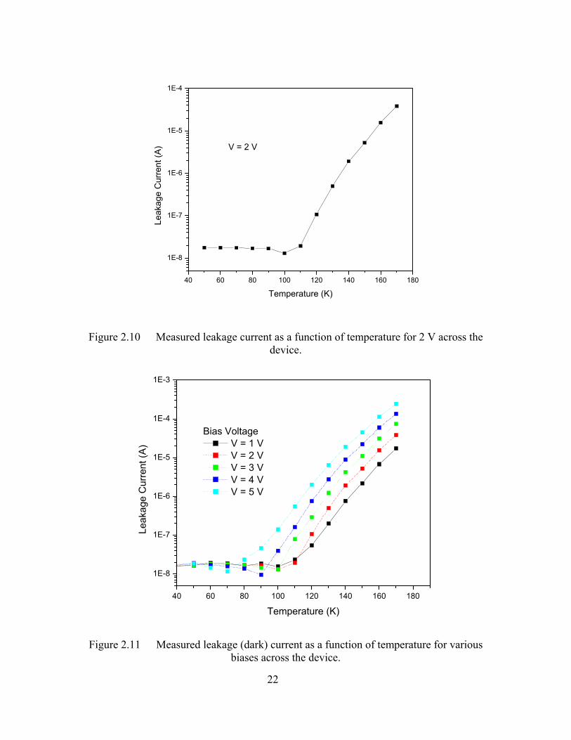
Figure 2.10 Measured leakage current as a function of temperature for 2 V across the device. ............................................................................................................. 22
Figure 2.11 Measured leakage (dark) current as a function of temperature for various biases across the device................................................................................... 22
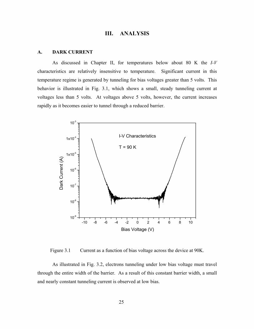
Figure 3.1 Current as a function of bias voltage across the device at 90K....................... 25
ix

Figure 3.2 Sequential tunneling under low bias voltage................................................... 26 Figure 3.3 Triangular tunneling under high bias voltage. ................................................ 26 Figure 3.4 Current as a function of bias voltage across the device at 50K, 100K, and
150K. ............................................................................................................... 27 Figure 3.5 Schematic diagram of the quantum well under an external bias showing
both tunneling and thermionic processes. ....................................................... 27 Figure 3.6 Physical dimensions and orientation of the QWIP device where L
represents its lateral dimensions. The layers are grown along the z-direction........................................................................................................... 29
Figure 3.7 Schematic diagram of the two-dimensional density of states. ........................ 30 Figure 3.8 Arrhenius plot of the leakage current. The straight line indicates the
thermionic nature of the current in the high temperature region..................... 34 Figure 3.9 Linear fit of the activation energies over a range of voltages. ........................ 35 Figure 3.10 Conceptual diagram of the conduction band offset, ............................ 37
maxCE∆Figure 3.11 Estimated ground state energy and conduction band offset using the
thermionic emission analysis. ......................................................................... 38 Figure 3.12 Photoresponse of detector at various wavelengths.......................................... 39 Figure 3.13 Detectivity at 5 µm versus temperature for set of bias voltages. .................... 41 Figure A.1 Energy state and wavefunction in finite potential well. The finite well is
extensively utilized in the design of semiconductor devices, particularly in quantum well based devices............................................................................ 47
x

LIST OF TABLES
Table 3.1 Bias voltages and corresponding activation energies V ........................ 35 B E− F
Table 3.2 Formulas for the energy bandgaps of AlGaAs and InGaAs compounds. ....... 37 Table 3.3 Device information provided by the optical experiments done by Zhou........ 39
xi

THIS PAGE INTENTIONALLY LEFT BLANK
xii

LIST OF SYMBOLS A area of device D* detectivity e electron charge
CE∆ conduction band offset maxCE∆ maximum conduction band offset
EF Fermi energy Eg band gap E0 ground state energy
max0E maximum ground state energy
F(E) Fermi function f∆ bandwidth
G optical gain g(E) density of states ħ reduced Planck’s constant Id dark current iN noise current Ip photocurrent I-V current-voltage I(T) temperature dependent dark current k Boltzmann’s constant k(x,y,z) wave vector (in x, y, and z direction) L(w,z) well width
wm∗ electron effective mass in well nD three-dimensional density of carriers in the well NEP noise equivalent power n(T) number of thermally generated charge carriers N2D two-dimensional density of carriers in the well QWIP quantum well infrared photodetector R responsivity T temperature T0 characteristic temperature VB barrier height
PΦ incident power ψ wave function
xiii

THIS PAGE INTENTIONALLY LEFT BLANK
xiv
ACKNOWLEDGMENTS
I am pleased to thank Professor Gamani Karunasiri, whose intelligence might only be surpassed by his kindness and generosity, for the guidance he provided me time and time again. Thanks are also due to Professor James Luscombe for his insights; to Mr. Kevin Lantz for his generous help, especially in the use of Matlab; and to Mr. Sam Barone for his electronic expertise and good humor. As always, my family deserves my utmost appreciation in many more ways than they could imagine.
xv

THIS PAGE INTENTIONALLY LEFT BLANK
xvi
I. INTRODUCTION
A. INTRODUCTION
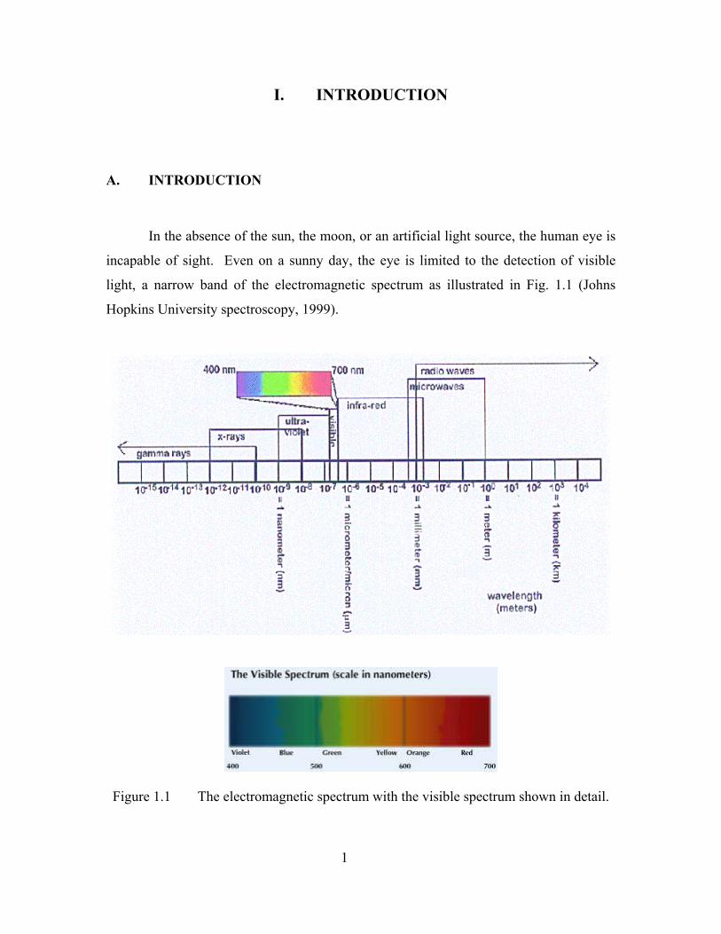
In the absence of the sun, the moon, or an artificial light source, the human eye is
incapable of sight. Even on a sunny day, the eye is limited to the detection of visible
light, a narrow band of the electromagnetic spectrum as illustrated in Fig. 1.1 (Johns
Hopkins University spectroscopy, 1999).
Figure 1.1 The electromagnetic spectrum with the visible spectrum shown in detail.
1

We detect visible light scattered from our surroundings as well as light from
objects hot enough to radiate in the visible, yet anyone who has walked on a dark night
knows how scarce the latter source can be. Were we able to shift our focus down the
spectrum to the infrared band, however, we would observe all terrestrial objects of finite
temperature with no dependence on visible light reflection. “Seeing” in the infrared is
what all infrared imaging systems seek to do, and applications of this technology range
from the military to the medical to the astronomical.
Infrared imaging systems operate by converting incident radiation into detectable
electric signals. There are two main detection mechanisms: the thermal and the photon.
Incident radiation changes the electrical properties in both types. For example, when
subject to infrared radiation, thermal detectors undergo a measurable change in their
electrical resistance. In addition, pyroelectric and thermoelectric effects can also be used.
On the other hand, a photon detector generates electron-hole pairs, yielding a measurable
photocurrent proportional to the incident radiation power. However, photon detectors
must be cooled significantly to reduce the dark current associated with the thermal
excitation of carriers. Despite this requirement, at low operating temperatures (less than
80 K) such devices have a responsivity and detectivity superior to that of thermal
detectors (Ting, 1999, pp. 2).
Although thermal detectors are advantageous in their ability to operate near room
temperature, in terms of speed and sensitivity their cooled photon detector counterparts
generally prove to be the better imaging systems. The desired wavelength detection
range includes important bands suffering a minimum of atmospheric absorption (3-5 and
8-12 µm). Furthermore, near 300 K ambient temperature blackbody radiation is brightest
in the 8-12 µm range. The 3-5 µm detection is usually achieved by indium antimonide
(InSb) and the 8-12 µm band is covered using mercury cadmium telluride (HgCdTe,
known commonly as “MCT”) detectors. The Quantum Well Infrared Photodetector
(QWIP) has evolved as a useful detector in the 2-35 µm range (Gunapala et al., 2002)
due to the possibility of having excellent uniformity in large area arrays. In this project,
the operation parameters of a 3-5 µm QWIP will be experimentally investigated in order
to optimize its performance.
2
B. STRUCTURAL CONSIDERATIONS
As previously mentioned, the important wavelength bands for infrared detection
are 3-5 µm and 8-12 µm. The primary mechanism of the infrared photon detector is
based on the photoexcitation of charge carriers across a band gap, Eg. The longer the
detection wavelength, the narrower a band gap is required. From our extensive
experience with visible light (roughly 400-800 nm) we know that silicon (Si, Eg = 1.1 eV)
has shown to be an ideal detector of it. However, the difficulty of making adequate
detectors for the desirable infrared wavelengths results from the lack of materials having
band gaps in the 0.1 – 0.4 eV range.
Though materials such as InSb (Eg = 0.2 eV) and mercury cadmium telluride
(HgCdTe, Eg = 0.1 eV) have sufficiently small band gaps, they ordinarily present
difficulties in their material stability, uniformity, and reproducibility, particularly in
comparison with larger-band-gap devices such as Si and gallium arsenide (GaAs). This
difficulty prompted the use of heterostructures made of large gap semiconductors in the
fabrication of infrared detectors (Levine, 1993, pp. R3). An AlGaAs/GaAs
heterostructure and the resulting well structure are illustrated schematically in Fig. 1.2.
3

AlxGa1-xAs AlxGa1-xAsGaAsEn
ergy
Eg(AlGaAs) (BARRIER)
EC(AlGaAs)
EV(AlGaAs)
EC(GaAs)
EV(GaAs)
Eg(GaAs) (WELL)
EC
EV
• • • • • • •E0
E1
H0H1
Figure 1.2 Schematic band structure of quantum-well with intersubband transitions of
electrons and holes shown.
A typical QWIP is composed of alternating layers of two different
semiconductors. A thin layer of a smaller bandgap semiconductor (i.e. GaAs) is placed
between two layers of a larger bandgap material (i.e. AlxGa1-xAs), thus creating a
quantum well. Such a structure can be obtained by growing the layers alternately using
Molecular Beam Epitaxy (MBE) or Metal Organic Vapor Deposition (MOCVD). The
growth of thin layers using MBE is schematically depicted in Fig. 1.3.
4

Figure 1.3 MBE system in which beams of molecules or atoms are used to deposit material on a heated substrate at an ultra high vacuum condition of less than 10-10 torr
base pressure.
The question still remains: How can large band gap materials such as Si and GaAs
be used to detect the relatively long infrared wavelengths? In a quantum well, absorption
results in transitions between the quantized energy states within the same band
(intersubband) rather than the more familiar transition between the valence and
conduction bands (interband). That is, the QWIP detects infrared radiation by exciting
bound electrons within the quantum wells created in the heterostructure. Both the
physical situation and the intersubband transition are shown in Fig. 1.4.
EV EC
AlxGa1-xAs
AlxGa1-xAs
GaAs
GaAs substrate
E1
E0
EC
•
••
Figure 1.4 Single quantum well (a) physical structure and (b) simplified band structure. 5
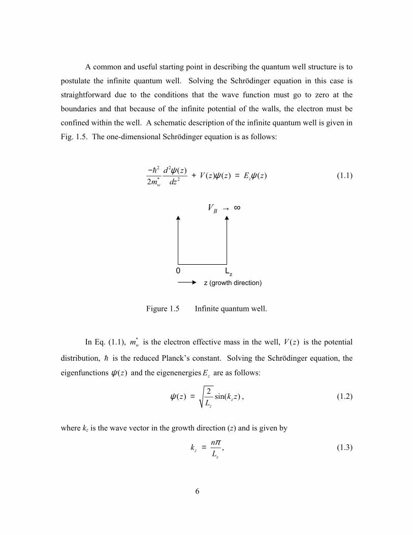
A common and useful starting point in describing the quantum well structure is to
postulate the infinite quantum well. Solving the Schrödinger equation in this case is
straightforward due to the conditions that the wave function must go to zero at the
boundaries and that because of the infinite potential of the walls, the electron must be
confined within the well. A schematic description of the infinite quantum well is given in
Fig. 1.5. The one-dimensional Schrödinger equation is as follows:
2 2
* 2
( ) ( ) ( ) ( )2 z
w
d z V z z E zm dz
ψ ψ ψ− + = (1.1)
z (growth direction)
0 Lz
BV → ∞
Figure 1.5 Infinite quantum well.
In Eq. (1.1), is the electron effective mass in the well, V z is the potential
distribution, is the reduced Planck’s constant. Solving the Schrödinger equation, the
eigenfunctions
*wm
)
( )
(zψ and the eigenenergies are as follows: zE
2( ) sin( )zz
zL
ψ = k z , (1.2)
where kz is the wave vector in the growth direction (z) and is given by
zz
nkLπ= , (1.3)
6

and
2 2
*2z
zw
kEm
= . (1.4)
It can be seen that the eigenenergy between the first and second energy level is
dependent on . Thereby the well width becomes an important design parameter used to
select the wavelength a given QWIP “sees”. In addition, the width of the well also
determines the location of the excited state relative to the barrier height in the case of a
finite potential. There are two principle types of QWIP, each determined by the location
of the excited state: bound-to-bound and bound-to-continuum. The QWIP studied in this
thesis is a bound-to-continuum type.
zL
In a bound-to-continuum QWIP, the required detector wavelength is obtained by
adjusting the well width such that the first energy level occurs in the well and the
subsequent states form a continuum band just above the well as illustrated in Fig. 1.6.
••
••
••
Figure 1.6 Band diagram of bound-to-continuum quantum well structure showing the
excitation of electrons to the continuum band.
Thus, when a photon is incident with energy at least equal to the energy difference
between the first bound state and the continuum state, it will be absorbed by an electron
in the well that will undergo a transition to the continuum band. If a bias is placed across
the device, the excited electron drifts under the field, forming a photocurrent proportional
to the initial incident infrared radiation intensity.
7

•
•
•
•
••
Figure 1.7 Band diagram of bound-to-bound quantum well structure showing the excitation of electrons and their subsequent tunneling through the barrier.
In a bound-to-bound quantum well structure, shown schematically in Fig. 1.7,
electrons are excited from the first bound state to the second bound state, then tunnel out
through the barrier under an applied electric field and form a photocurrent. The well
parameters are designed such that the barriers are thick enough to reduce the tunneling
current through the ground levels (i.e., up to 500 Å). The excited electrons then tunnel
through the triangular barrier formed due to the external bias (see Fig. 1.7). Furthermore,
the position of the excited state is based on several considerations: the transport of
photoelectrons, the absorption strength, and the dark current. The main limitation of
QWIP devices is the presence of this dark current, which limits the detectors’ sensitivities
at higher operating temperatures.
Generally, the intrinsic electron concentration in the well is too low for the
generation of sufficient photocurrent. Hence, the wells are typically doped with silicon to
provide adequate charge carriers. At room temperature these carriers easily “boil off”
due to thermal excitation, forming a large dark current even in the absence of incident
radiation. It is because of this thermionic emission and the consequent dark current that
we must cool the QWIP to a low temperature for it to be an effective detector.
Countless combinations of factors ranging from the material properties of the
semiconductors to the consideration of operational temperature underlie the difficult task
of establishing the optimal structural and operating parameters for a specific QWIP
application. Researchers have been working on these matters for nearly thirty years
(Levine, 1993, pp. R3).
8

C. PRESENT STATUS OF QWIPS
Before the availability of modern growth techniques, Esaki et al. proposed
research on the quantum effects of semiconductor heterostructures in 1969. The use of
larger-band-gap heterostructures as an alternative to the inadequate InSb and HgCdTe
type devices was first proposed by Esaki and Sakaki in 1977. A number of experimental
(Smith et al. and Chiu et al., both 1983) and theoretical (Coon, Karunasiri, and Liu, 1984
and 1985) investigations followed, leading up to the first observation of strong
intersubband absorption in GaAs/AlGaAs quantum wells by West et al. in 1985.
The earliest working QWIP was designed soon after by Levine et al. (1987).
Again, it was a GaAs/AlGaAs device and was based on bound-to-bound transitions. The
photoelectrons in this first device had to tunnel through relatively large barriers, a
limitation that yielded an extremely low responsivity. Bound-to-bound shortcomings led
to the use of bound-to-continuum transitions, which were first proposed by Coon and
Karunasiri in 1984. The first bound-to-continuum QWIP was demonstrated to have a
much higher responsivity (Hasnain et al., 1989), but also a small peak absorbance due to
the weak oscillator strength above the well.
Further advances in QWIP design have led to structures that are based on bound-
to-quasi-continuum transitions (Levine et al., 1991), bound-to-miniband transitions (Yu
et al., 1991) and bound-to-quasi-bound transitions (Gunapala et al., 1996). These more
recent configurations have shown good detector performance due to the fact that in all of
these cases the ground state electrons do not flow in response to an external bias while
the photoelectrons can create a photocurrent with the use of a relatively small bias.
Multiple structural optimizations have also been made that improve QWIP performance.
Increasing the barrier width has reduced the tunneling current by many orders of
magnitude (Levine et al., 1991) while lowering the excited state from the continuum into
the quasi-bound region has been shown to reduce the dark current from thermionic
emission by a factor of roughly 12 at 70K (Gunapala et al., 1996). It has also been found
that adding a grating on top of the device and thereby increasing the electric field
9
polarization normal to the quantum wells substantially increases absorption strength
(Gunapala et al., 1996).
D. MILITARY RELEVANCE
The QWIP is of particular relevance in today’s military because of its capabilities
as both an infrared imager and as a laser spot tracker for use in laser-guided weapons
delivery. Quantum well structures can be designed capable of detecting wavelengths as
low as 1 µm, and as such they can be tuned to detect standard NATO/U.S. combat laser
designation wavelengths. In addition to this powerful capability, quantum wells can be
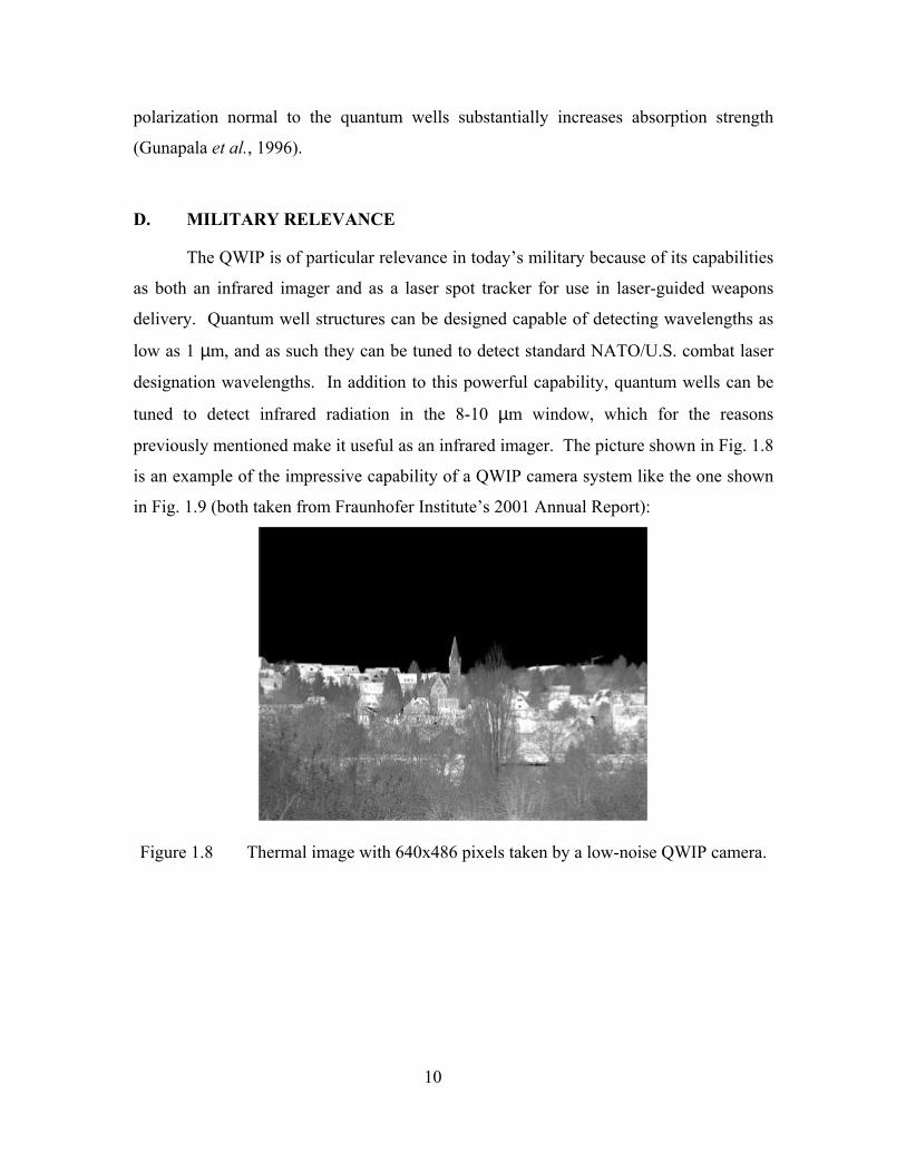
tuned to detect infrared radiation in the 8-10 µm window, which for the reasons
previously mentioned make it useful as an infrared imager. The picture shown in Fig. 1.8
is an example of the impressive capability of a QWIP camera system like the one shown
in Fig. 1.9 (both taken from Fraunhofer Institute’s 2001 Annual Report):
Figure 1.8 Thermal image with 640x486 pixels taken by a low-noise QWIP camera.
10
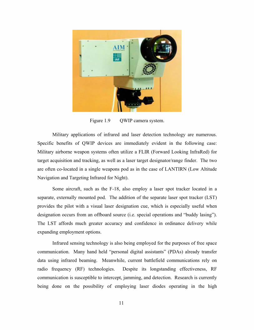
Figure 1.9 QWIP camera system.
Military applications of infrared and laser detection technology are numerous.
Specific benefits of QWIP devices are immediately evident in the following case:
Military airborne weapon systems often utilize a FLIR (Forward Looking InfraRed) for
target acquisition and tracking, as well as a laser target designator/range finder. The two
are often co-located in a single weapons pod as in the case of LANTIRN (Low Altitude
Navigation and Targeting Infrared for Night).
Some aircraft, such as the F-18, also employ a laser spot tracker located in a
separate, externally mounted pod. The addition of the separate laser spot tracker (LST)
provides the pilot with a visual laser designation cue, which is especially useful when
designation occurs from an offboard source (i.e. special operations and “buddy lasing”).
The LST affords much greater accuracy and confidence in ordinance delivery while
expanding employment options.
Infrared sensing technology is also being employed for the purposes of free space
communication. Many hand held “personal digital assistants” (PDAs) already transfer
data using infrared beaming. Meanwhile, current battlefield communications rely on
radio frequency (RF) technologies. Despite its longstanding effectiveness, RF
communication is susceptible to intercept, jamming, and detection. Research is currently
being done on the possibility of employing laser diodes operating in the high
11
transmission mid-wave infrared (MWIR) 3 – 5 µm range to provide very high bandwidth
free space optical communication.
The medical market for QWIP technology is also of obvious interest to the
military. Breast cancer detection is only one example of QWIP medical applicability. In
this case, slight changes of the skin temperature in the vicinity of a tumor can be detected.
Fraunhofer IAF reports that to achieve this end, thermal deviations with a modulation
frequency of 0.1 – 2 Hz must be detected. Clearly infrared and laser technology is at the
heart of many critical military applications. As this promises to be the case well into the
future, QWIP applications will continue to be of significant interest to the military.
12

II. EXPERIMENTAL
A. TEST SETUP
The title of this thesis disguises one of the main purposes of my work, which was
to set up a low temperature current-voltage (I-V) measurement system. The task of
supply gathering and setup proved considerably more difficult than finally running the
experiment. Consequently, this section is tantamount to an operational manual
describing that portion of the lab pertaining to my research. It is my hope that it will be
useful to future students.
The experimental setup for the measurement of I-V characteristics under varying
temperature is given schematically in Fig. 2.1 and the various components are described
in detail below.
Turbo-Pump
Compressor
4155B SemiconductorParameter Analyzer
Keyboard
"Bus"Test
Fixture
TemperatureController
He Lines
PressureGauge
Ref
riger
ator
Experimental Setup
Cold Head
Water CoolingLines
Figure 2.1 Schematic diagram of the low temperature I-V characterization system.
13
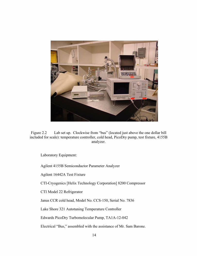
Figure 2.2 Lab set up. Clockwise from “bus” (located just above the one dollar bill included for scale): temperature controller, cold head, PicoDry pump, test fixture, 4155B
analyzer.
Laboratory Equipment:
Agilent 4155B Semiconductor Parameter Analyzer
Agilent 16442A Test Fixture
CTI-Cryogenics [Helix Technology Corporation] 8200 Compressor
CTI Model 22 Refrigerator
Janus CCR cold head, Model No. CCS-150, Serial No. 7836
Lake Shore 321 Autotuning Temperature Controller
Edwards PicoDry Turbomolecular Pump, TA1A-12-042
Electrical “Bus,” assembled with the assistance of Mr. Sam Barone.
14
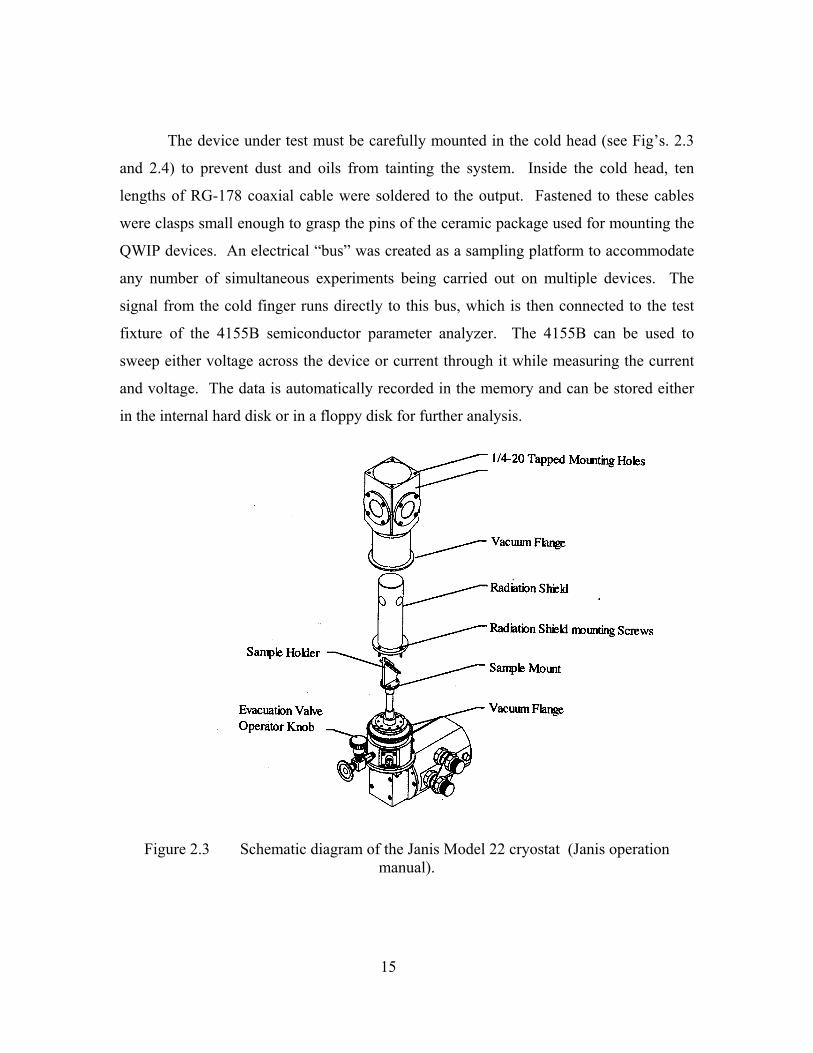
The device under test must be carefully mounted in the cold head (see Fig’s. 2.3
and 2.4) to prevent dust and oils from tainting the system. Inside the cold head, ten
lengths of RG-178 coaxial cable were soldered to the output. Fastened to these cables
were clasps small enough to grasp the pins of the ceramic package used for mounting the
QWIP devices. An electrical “bus” was created as a sampling platform to accommodate
any number of simultaneous experiments being carried out on multiple devices. The
signal from the cold finger runs directly to this bus, which is then connected to the test
fixture of the 4155B semiconductor parameter analyzer. The 4155B can be used to
sweep either voltage across the device or current through it while measuring the current
and voltage. The data is automatically recorded in the memory and can be stored either
in the internal hard disk or in a floppy disk for further analysis.
Figure 2.3 Schematic diagram of the Janis Model 22 cryostat (Janis operation manual).
15
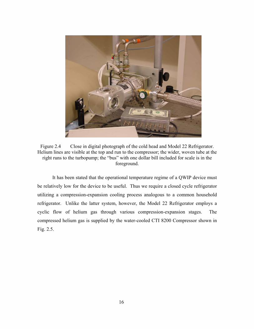
Figure 2.4 Close in digital photograph of the cold head and Model 22 Refrigerator.
Helium lines are visible at the top and run to the compressor; the wider, woven tube at the right runs to the turbopump; the “bus” with one dollar bill included for scale is in the
foreground.
It has been stated that the operational temperature regime of a QWIP device must
be relatively low for the device to be useful. Thus we require a closed cycle refrigerator
utilizing a compression-expansion cooling process analogous to a common household
refrigerator. Unlike the latter system, however, the Model 22 Refrigerator employs a
cyclic flow of helium gas through various compression-expansion stages. The
compressed helium gas is supplied by the water-cooled CTI 8200 Compressor shown in
Fig. 2.5.
16
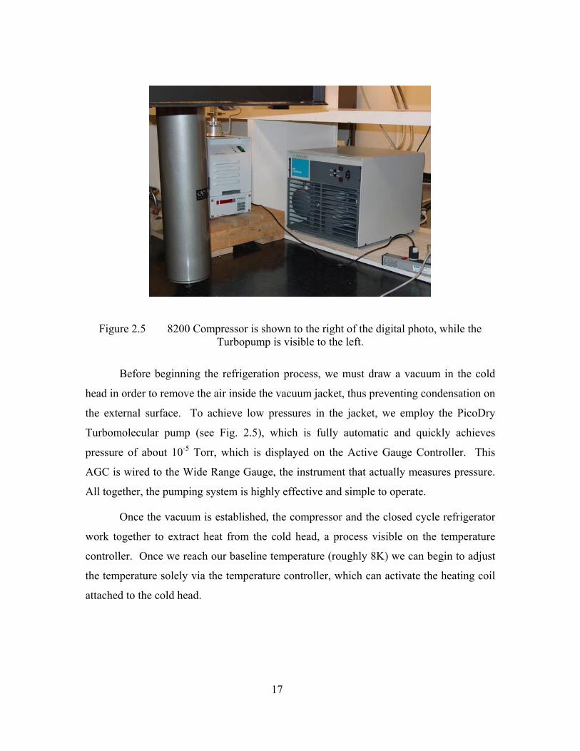
Figure 2.5 8200 Compressor is shown to the right of the digital photo, while the Turbopump is visible to the left.
Before beginning the refrigeration process, we must draw a vacuum in the cold
head in order to remove the air inside the vacuum jacket, thus preventing condensation on
the external surface. To achieve low pressures in the jacket, we employ the PicoDry
Turbomolecular pump (see Fig. 2.5), which is fully automatic and quickly achieves
pressure of about 10-5 Torr, which is displayed on the Active Gauge Controller. This
AGC is wired to the Wide Range Gauge, the instrument that actually measures pressure.
All together, the pumping system is highly effective and simple to operate.
Once the vacuum is established, the compressor and the closed cycle refrigerator
work together to extract heat from the cold head, a process visible on the temperature
controller. Once we reach our baseline temperature (roughly 8K) we can begin to adjust
the temperature solely via the temperature controller, which can activate the heating coil
attached to the cold head.
17
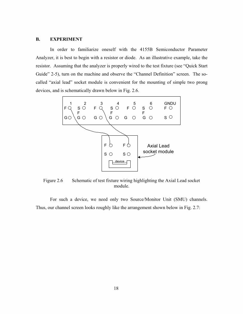
B. EXPERIMENT
In order to familiarize oneself with the 4155B Semiconductor Parameter
Analyzer, it is best to begin with a resistor or diode. As an illustrative example, take the
resistor. Assuming that the analyzer is properly wired to the test fixture (see “Quick Start
Guide” 2-5), turn on the machine and observe the “Channel Definition” screen. The so-
called “axial lead” socket module is convenient for the mounting of simple two prong
devices, and is schematically drawn below in Fig. 2.6.
1 2 3 4 5 6 GNDUF S F S F S F F F FG G G G G G S
F F
S S
device
Axial Leadsocket module
Figure 2.6 Schematic of test fixture wiring highlighting the Axial Lead socket module.
For such a device, we need only two Source/Monitor Unit (SMU) channels.
Thus, our channel screen looks roughly like the arrangement shown below in Fig. 2.7:
18

CHANNELS: CHANNEL DEFINITION
*MEASUREMENT MODE
*CHANNELS
MEASURE
UNIT VNAME INAME MODEMODE FCTNSTBY
SMU1:MPSMU2:MPSMU3:MPSMU4:MPSMU5:MPSMU6:MPVSU1VSU2VMU1VMU2PGU1PGU2GNDU
VF
V
IF
I
V
COMMON
VAR1
CONST
SAMPLING
Figure 2.7 Channel configuration for a basic “two-pronged” device.
This same configuration can also be arrived at by simply pushing the “MEM4 /
DIODE / VF-IF” memory softkey. Continue by pushing the “next page” softkey, which
calls up first the “USER FUNCTION DEFINITION,” then the “SWEEP SETUP,” and
finally the “DISPLAY SETUP” pages, on which we can define names, units, etc.; change
the increments of the sweep; and alter graph range and domain, respectively. For the
simple purpose of successfully viewing the I-V characteristics of the resistor, we can
simply bypass these screens. On the “GRAPH” page, press the “SINGLE” button in the
upper right-hand side of the panel to test the device. The cursor should move across the
screen leaving a yellow line. To adjust the scaling, simply press the “SCALING” and
19

then the “AUTO SCALING” softkeys. This should yield the linear lineshape we expect
from a resistor as illustrated in Fig. 2.8.
0.0 0.5 1.0 1.5 2.00
5
10
15
20
25
30
35C
urre
nt (m
icro
A)
Voltage (V)
I-V characteristics for 62 kilo ohm resistor
Figure 2.8 Measured I-V characteristics using Agilent 4155B parameter analyzer for
a 62 kΩ resistor.
For a QWIP, the process is remarkably similar, with an identical channel
arrangement except that the signals come from the external bus rather than from the
socket module within the test fixture.
C. I-V AS A FUNCTION OF TEMPERATURE
The purpose of this project is to carry out a detailed study of the dark condition I-
V characteristics of an AlGaAs/InGaAs, 3-5 µm QWIP as a function of temperature in
order to determine the quantized energy levels and performance parameters. The QWIP
structure used in this study consists of 25 periods of 23 nm thick Al0.37Ga0.63As barrier
and 3.6 nm well. The entire quantum well structure is sandwiched between 1 µm GaAs
buffers and 0.5 µm GaAs cap layers, which are doped to 1018 cm-3. The I-V measurement 20

was carried out over a temperature range of 10 to 170 K using 200 by 200 µm2 mesa
diodes.
Measured I-V characteristics of the QWIP sample between 10 and 170 K are
shown in Fig. 2.9. During the measurement, the device was covered using a cold shield
to eliminate the photocurrent generated by background thermal radiation. The I-V
characteristics shown in Fig. 2.9 are relatively insensitive to temperature below 80 K,
while in the high temperature regime they show strong temperature dependence. The
dramatic reduction of the dark current at low temperatures is largely due to the decrease
of thermionic emission.
-10 -8 -6 -4 -2 0 2 4 6 8 10
1E-8
1E-7
1E-6
1E-5
1E-4
1E-3
Dar
k C
urre
nt (A
)
Bias Voltage (V)
I10K I50K I60K I70K I80K I90K I100K I110K I120K I130K I140K I150K I160K I170K
Figure 2.9 Measured I-V characteristic curve over temperature range of 10 to 170K. The symmetry of the I-V characteristics is due to the unipolar nature of the QWIP
structure (n-i-n).
21
40 60 80 100 120 140 160 180
1E-8
1E-7
1E-6
1E-5
1E-4
Leak
age
Cur
rent
(A)
Temperature (K)
V = 2 V
Figure 2.10 Measured leakage current as a function of temperature for 2 V across the device.
40 60 80 100 120 140 160 180
1E-8
1E-7
1E-6
1E-5
1E-4
1E-3
Leak
age
Cur
rent
(A)
Temperature (K)
Bias Voltage V = 1 V V = 2 V V = 3 V V = 4 V V = 5 V
Figure 2.11 Measured leakage (dark) current as a function of temperature for various
biases across the device.
22
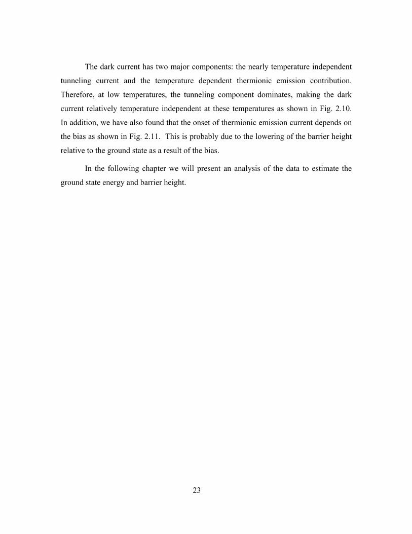
The dark current has two major components: the nearly temperature independent
tunneling current and the temperature dependent thermionic emission contribution.
Therefore, at low temperatures, the tunneling component dominates, making the dark
current relatively temperature independent at these temperatures as shown in Fig. 2.10.
In addition, we have also found that the onset of thermionic emission current depends on
the bias as shown in Fig. 2.11. This is probably due to the lowering of the barrier height
relative to the ground state as a result of the bias.
In the following chapter we will present an analysis of the data to estimate the
ground state energy and barrier height.
23

THIS PAGE INTENTIONALLY LEFT BLANK
24
III. ANALYSIS
A. DARK CURRENT
As discussed in Chapter II, for temperatures below about 80 K the I-V
characteristics are relatively insensitive to temperature. Significant current in this
temperature regime is generated by tunneling for bias voltages greater than 5 volts. This
behavior is illustrated in Fig. 3.1, which shows a small, steady tunneling current at
voltages less than 5 volts. At voltages above 5 volts, however, the current increases
rapidly as it becomes easier to tunnel through a reduced barrier.
-10 -8 -6 -4 -2 0 2 4 6 8 1010-9
10-8
10-7
10-6
1x10⁻⁵
1x10⁻⁴
10-3
Dar
k C
urre
nt (A
)
Bias Voltage (V)
I-V Characteristics T = 90 K
Figure 3.1 Current as a function of bias voltage across the device at 90K.
As illustrated in Fig. 3.2, electrons tunneling under low bias voltage must travel
through the entire width of the barrier. As a result of this constant barrier width, a small
and nearly constant tunneling current is observed at low bias.
25

• ••• ••
• ••
Figure 3.2 Sequential tunneling under low bias voltage.
In the simplified sketch of the bias effect shown in Fig. 3.3, the relative ease of
“triangular” tunneling at high bias as compared to low bias voltage is evident. In this
case, the effective barrier width is shortened by the high bias effect and consequently a
greater tunneling current is observed.
•
• •
••
•
• ••
Figure 3.3 Triangular tunneling under high bias voltage.
As seen in Fig. 3.4, as the temperature of our device rises, tunneling current can
quickly cease to be the primary contribution to the dark current. Although tunneling
current still takes place and continues to be influential at high bias voltages, thermionic
emission accounts for the rapid rise in dark current between 100 K to 150 K. Though it is
true that tunneling is relatively temperature insensitive, thermally assisted tunneling does
take place, accounting for the sharp rise at 4 V of the 100 K (compared to 6 V at 50 K)
26

curve in Fig. 3.4. Both the tunneling and the thermionic emission contributions to dark
current are schematically illustrated in Fig. 3.5.
-10 -8 -6 -4 -2 0 2 4 6 8 1010-9
10-8
10-7
10-6
1x10⁻⁵
1x10⁻⁴
10-3
T = 150 K
T = 100 K
T = 50 KDar
k C
urre
nt (I
)
Bias Voltage (V)
Figure 3.4 Current as a function of bias voltage across the device at 50K, 100K, and 150K.
CE∆EFE0
VB
LW LB
Tunneling
Thermionic Emission•
•
Figure 3.5 Schematic diagram of the quantum well under an external bias showing both tunneling and thermionic processes.
27

As mentioned, the I-V characteristics show strong temperature dependence in the
high temperature region (above 100 K) as thermionic emission rises with increasing
temperature, thereby dominating the relatively temperature-insensitive tunneling current.
At low temperatures, however, thermionic emission is greatly reduced and tunneling
current is most prominent. For these reasons, a thermionic emission model was chosen to
analyze the high temperature region I-V data.
B. THERMIONIC EMISSION
Thermionic emission can provide significant information, including an estimation
of the conduction band offset and the ground state energy, provided the quasi-Fermi level
EF (as shown above in Fig. 3.5) of the carriers in the well is known. For low
temperatures ( kT < EF ), EF is given by (Karunasiri, 1996)
2
*
ћD wF
w
n LEm
π= (3.1)
where Dn is the density of the carriers in the well, is the reduced Planck’s constant,
is the effective mass of an electron in the well, and is the width of the well.
ћ
L
*wm
w
To arrive at EF, we must first find the two-dimensional density of states, g(E),
which is defined such that g(E)dE is the number of states in the energy interval E to (E +
dE) per unit area of the sample due to free motion of electrons parallel to the layers of the
quantum well, as illustrated in Fig. 3.6.
28
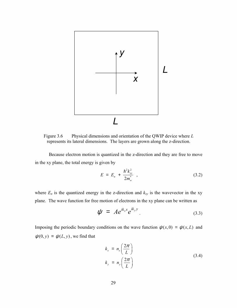
L
L
x
y
Figure 3.6 Physical dimensions and orientation of the QWIP device where L represents its lateral dimensions. The layers are grown along the z-direction.
Because electron motion is quantized in the z-direction and they are free to move
in the xy plane, the total energy is given by
2 2
*2xy
nw
kE E
m= + , (3.2)
where En is the quantized energy in the z-direction and kxy is the wavevector in the xy
plane. The wave function for free motion of electrons in the xy plane can be written as
yx ik yik xAe eψ = . (3.3)
Imposing the periodic boundary conditions on the wave function ( ,0) ( , )x x Lψ ψ= and
(0, ) ( , )y L yψ ψ= , we find that
2
2
x x
y y
k nL
k nL
π
π
= =
(3.4)
29
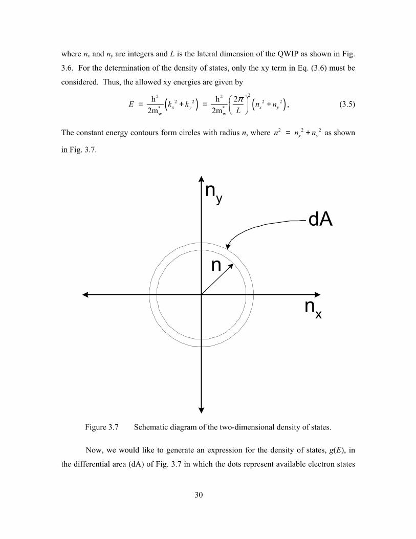
where nx and ny are integers and L is the lateral dimension of the QWIP as shown in Fig.
3.6. For the determination of the density of states, only the xy term in Eq. (3.6) must be
considered. Thus, the allowed xy energies are given by
( ) (22 2
2 2 2 2* *w w
ћ ћ 22m 2mx y x yE k k n
Lπ = + = +
)n
2y
, (3.5)
The constant energy contours form circles with radius n, where as shown
in Fig. 3.7.
2 2xn n n= +
ny
nx
dA
n
Figure 3.7 Schematic diagram of the two-dimensional density of states.
Now, we would like to generate an expression for the density of states, g(E), in
the differential area (dA) of Fig. 3.7 in which the dots represent available electron states
30

between E and E + dE. Because each energy state occupies unity space in the n-space,
the total number of states between E and E + dE is given by
, (3.6) ( ) 2 2G E dE ndnπ= ×
where the leading factor of two accounts for the spin degeneracy. Using Eq. (3.5) we can
rewrite Eq. (3.6) in terms of energy as
* 2 *
22( ) 4
4 ћ ћwm L mG E dE dE L dEπ
π π= = 2
w . (3.7)
Dividing by area (given by ) we arrive at the following expression for the density of
states (i.e., the number of states per unit area over energy):
2L
*
2( )ћwmg E
π= . (3.8)
To find the quasi-Fermi energy level, , we must know two-dimensional
electron density, N
FE
2D, in the well. This can be easily obtained using the three-
dimensional density, Dn , using the relation
2D D wN n= L . (3.9)
It is often the case that both Dn (~1018 cm-3) and the well width, , are known, so that
we can find
wL
2DN directly by plugging into Eq. (3.9). The quasi-Fermi Energy can be
found by first integrating the density of available states, , multiplied by the
probability of occupation at a given energy, , and equating it to
( )g E
( )F E 2DN as follows:
(3.10) 2 0( ) ( )DN F E g E
∞= ∫ dE
In the above integral, the energy is measured from the ground state of the
quantum well and the occupation probability is given by the Fermi-Dirac distribution
function, F(E):
1( )( )1 exp F
F EE E
kT
=− +
, (3.11)
31

where k is Boltzmann’s constant and T is the temperature. Using the Fermi function, the
above integral can be written as
( )* *
2 ( ) ( )2 20 0
1
1 1
F
F F
E EkT
w wD E E E E
kT kT
m m eN dEe e
π π
− −
∞ ∞
− − −
= =
+ + ∫ ∫ dE . (3.12)
Carrying out the integral and substituting the limits, we find that
*
2 2 ln(1 )FE
w kTD
mN kT eπ
= +
. (3.13)
Solving for the Fermi energy, we obtain the following:
22*
ln 1D
w
NkTm
FE kT eπ
= −
. (3.14)
It can easily be seen that when
2
20*
D
w
NTkm
π< T= , (3.15)
the Fermi energy is independent of temperature and is given by
2
2*Fw
Emπ= DN . (3.16)
In our experiment, the detector structure was designed having In0.1Ga0.9As wells with
doping density (nd) of 1018 cm-3. Using Vegard’s Law we can interpolate the effective
mass of an electron in the InxGa1-xAs layer as (Singh, 1993, pp. 185)
1
1 (
x xIn Ga As InAs GaAs
1 )x xm m m
−
∗ ∗
−= + ∗ (3.17)
32
where and m are the effective masses of electrons in
InAs and in GaAs, respectively. This gives a value for the effective mass in the
In
InAs em = 0.028m ∗GaAs e0.067 m∗ =
0.1Ga0.9As well of 0.059me. Using the well width Lw = 3.6 nm we calculate the value of
2DN to be 3.6 cm1110× -2, while the characteristic temperature (T0) with a constant Fermi
energy is found to be about 170 K. Thus, for the temperature range over which the
experiment was carried out, the quasi-Fermi energy is independent of temperature.
In order to estimate the dark current it is necessary to estimate the number of
thermally excited electrons, n(T), above the barrier. This can be obtained from Eq. (3.14)
as
. (3.18) ( ) ( ) ( )BV
n T F E g E dE∞
= ∫
For these electrons, >> kT and the Fermi function can be approximated by the
Boltzmann distribution:
FE E−
(( ) exp FE EF EkT−≈ −
) . (3.19)
Thus, the above integral reduces to
*
2
(( ) expћw B F
w
m kT V En TL kTπ
−= −
) (3.20)
where VB is the barrier height measured relative to the ground level.
C. THERMALLY GENERATED DARK CURRENT
As previously mentioned, our purpose here is to estimate the dark current, I(T),
generated by the thermal excitation of electrons from the well. The current density is
proportional to the number of thermally excited carriers. Thus, the dark current can be
estimated from the number of electrons having energies larger than the barrier height and
is given by
(( ) exp B FV EI TT k
− ∝ −
)T
. (3.21)
33

From this last expression we can find the activation energy V by plotting B E− F
( )ln I TT
versus 1/T. Fig. 3.8 shows the Arrhenius plot for measured current at 2 V bias
for temperatures in the 110 – 170 K range.
5.5 6.0 6.5 7.0 7.5 8.0 8.5 9.0 9.5
-23
-22
-21
-20
-19
-18
-17
-16
-15
ln I(
T)/T
(A/
K)
1000/T (1/K)
V = 2 V
Linear Fit
VB - EF = 192 meV
Figure 3.8 Arrhenius plot of the leakage current. The straight line indicates the thermionic nature of the current in the high temperature region.
The excellent linear fit to the data indicates the validity of Eq. (3.21) for describing the
dark current. The slope of the line ( )
1000B FV E
k
−
can be used for the estimation of the
activation energy V . For the determination of the ground state energy it is
necessary to find the barrier height, V
FB E−
B, at zero bias, as well as the Fermi energy.
The condition that allows us to estimate the Fermi energy using Eq.
(3.1). We find that
FkT < E
34
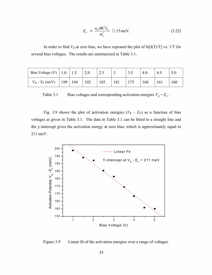
2
*
ћ 15D wF
w
n LEmπ= ≅ meV. (3.22)
In order to find VB at zero bias, we have repeated the plot of ln[I(T)/T] vs. 1/T for
several bias voltages. The results are summarized in Table 3.1.
Bias Voltage (V) 1.0 1.5 2.0 2.5 3 3.5 4.0 4.5 5.0
VB – EF (meV) 199 194 192 185 181 175 168 161 160
Table 3.1 Bias voltages and corresponding activation energies V E . B F−
Fig. 3.9 shows the plot of activation energies (VB – EF) as a function of bias
voltages as given in Table 3.1. The data in Table 3.1 can be fitted to a straight line and
the y-intercept gives the activation energy at zero bias, which is approximately equal to
211 meV.
1 2 3 4 5155
160
165
170
175
180
185
190
195
200
Activ
atio
n Po
tent
ial:
V B - E F (m
eV)
B ias Voltage (V)
Linear Fit
Y-intercept at VB - EF = 211 meV
Figure 3.9 Linear fit of the activation energies over a range of voltages.
35

Given that our zero bias activation energy is 211 meV, VB corresponding to the
zero bias condition is approximately 226 meV. However, this is as far as we can go
experimentally: the problem remains of how to estimate the conduction band offset. For
this calculation must be known, but paradoxically it seems that cannot be
estimated without the offset. In order to overcome this obstacle, we make use of the fact
that the maximum energy of the ground state, , occurs when the barrier height is
infinite. In this case, E
0E 0E
max0E
0 is given by
22
max0 *
w w
ћ2m
ELπ
=
. (3.23)
Using the given values of well width and effective mass, we find to be
approximately 490 meV. Because V is the height relative to the ground state, the upper
bound of the conduction band offset, , must be given by
max0E
B
∆ maxCE
22
max*w w
ћ 4902mC B BE V V
Lπ
∆ = + = +
meV. (3.24)
The physical situation is given schematically in Fig. 3.10.
VB
maxCE∆
EF
max0E
36

Figure 3.10 Conceptual diagram of the conduction band offset, . maxCE∆
Using this relation, in which we know VB experimentally and begin with the infinite
approximation of , we can numerically calculate the ground state energy
corresponding to the band offset of ∆ . Then, a new value for the conduction band
offset can be calculated by adding the V
max0E
maxCE
B to the ground state energy calculated using the
. This iterative procedure (Karunasiri, G., 1996) is continued until convergence is
obtained, providing both the band offset and ground state energy for a given V
maxCE∆
B . As
previously discussed, VB can be determined using the measured I-V data while the Fermi
energy, EF, can be estimated using device parameters. The method was carried out using
a Matlab program that is described in detail in the Appendix.
Using the iterative approach just described, the conduction band offset and
the ground state energy E
CE∆
0 are found to be 362 meV and 136 meV, respectively. To
check the validity of this data we can make use of the generally accepted approximation
of the conduction band offset between AlGaAs and InGaAs:
(3.25) (0.6 AlGaAS InGaAsC g gE E E∆ = − )
To find these values of Eg we use the following formulas (Casey and Panish, 1978),
which correspond to energy gap compositional dependence at 300 K:
Compound Eg (eV) AlxGa1-xAs 1.424 1.247x+ GaxIn1-xAs 0.36 1.064x+
Table 3.2 Formulas for the energy bandgaps of AlGaAs and InGaAs compounds.
In this way we find the Eg (AlxGa1-xAs) to be 1.885 eV while the Eg (GaxIn1-xAs)
is 1.32 eV. Using equation (3.25), we find that the empirical offset is about 340 meV.
This estimation is found to be well within 5% of our experimental value of roughly 360
meV. The following schematic in Fig. 3.11 displays the various energy values within the
quantum well structure derived from our experiment:
37

VB = 226 meV
E0 = 136 meV
maxCE∆
EF = 15 meV
= 362 meV
Figure 3.11 Estimated ground state energy and conduction band offset using the thermionic emission analysis.
D. DETECTIVITY (D*) AS A FUNCTION OF TEMPERATURE
There are two important parameters used for the quantification of the performance
of photodetectors: responsivity and detectivity. The responsivity is the output current
produced per watt of radiant optical power input,
[ / ]P
P
IR A W=Φ
, (3.26)
where Ip is the photocurrent and PΦ is the incident power on the device. As our
experiment is carried out in the dark condition, we utilize previously measured values for
the responsivity, R, for the same QWIP (Zhou, 2002). Fig. 3.12 displays the
photoresponse of the device as a function of wavelength. The peak of the responsivity
appears at 5 µm. Table 3.3 is also included, and contains additional device data found by
Zhou et al.
38

4.0 4.2 4.4 4.6 4.8 5.0 5.2 5.4 5.60.0
0.2
0.4
0.6
0.8
1.0
Device Photoresponse
Nor
mal
ized
Pho
to R
espo
nse
Wavelength (µm)
Figure 3.12 Photoresponse of detector at various wavelengths.
Transition Type
Peak Absorbance
Dark Current at 1.5 V, 20 k
Window Current at
1.5 V, 20 K
Peak Width of Photoresponse
Curve
Integrated Responsivity
At 2 V
B-C 1510 cm-1 2 × 10⁻¹⁰ A 2 × 10⁻⁹ A 26 meV 20 mA/W
Table 3.3 Device information provided by the optical experiments done by Zhou.
We estimate the sensitivity of the detector by estimating its detectivity. The
detectivity of a device is a measure of the smallest photon flux that can be measured, and
it is therefore dependent on detector noise. Detectivity is defined as
* [ /A f
D cmNEP
∆= ]Hz W , (3.27)
where the NEP (noise equivalent power) is the root-mean-square (rms) incident radiant
power that gives a photosignal equal to the noise (or signal-to-noise ratio of one), A is the
area of the detector, and f is the bandwidth of the amplifier used. Since a QWIP is
effectively a photoconductor, the predominant noise comes from the generation-
∆
39
recombination of carriers. The generation-recombination noise current (iN) can be
estimated using the measured dark current as
4Ni eGI= d f∆ , (3.28)
where e is the electron charge, G is the optical gain, and Id is the temperature dependent
dark current (Levine, 1993, pp. R25). Using Eq. (3.26), with Φ = , the noise
equivalent power can be obtained using the measured responsivity as
P NEP
NiNEPR
= . (3.29)
After incorporating these values for iN and the NEP into Eq. (3.27), we find that
*
4 d
ADeGI
= R . (3.30)
With a 1.5 volt bias across the device, R at 5 µm is found to be 0.030 A/W. The
area of the device is 200 mµ by 200 mµ , and as such A equals 200 mµ . The
commonly accepted value for gain in a QWIP device is 0.1 (Levine, 1993, pp. R26).
With these details in mind, the plot of the detectivity versus temperature was created and
is shown in Fig. 3.13. The variable in D* is the temperature dependent dark current at
different bias voltages.
40

0 20 40 60 80 100 120 140 160 180108
109
1010D
* (c
m*H
z1/2 /W
)
Temperature (K)
V = 1 V V = 2 V V = 3 V V = 4 V V = 5 V
Figure 3.13 Detectivity at 5 µm versus temperature for set of bias voltages.
It can be seen from Fig. 3.13 that the detectivity remains constant up to 100 K for
low bias voltages (less than 3 V). However, for bias voltages greater than 3 V the
detectivity degrades beyond 80 K due to excessive thermionic assisted tunneling. In
addition, at high temperatures (greater than 100 K) the detectivity drops rapidly due to
the exponential increase of the thermionic emission current. This measurement indicates
that the present device is not suitable for high quality imagery if the operating
temperature is beyond 80 K.
41

THIS PAGE INTENTIONALLY LEFT BLANK
42

IV. CONCLUSIONS
The I-V characteristics of a bound-to-continuum QWIP device with Al0.37Ga0.63As
barriers of 23 nm, In0.1Ga0.9As wells of 3.6 nm, and a doping density (nd) of 1018 cm-3
were gathered and analyzed for various temperatures. The device was cooled using a
closed cycle refrigerator and the data were analyzed using the Agilent 4155B
Semiconductor Parameter Analyzer. At low temperatures the leakage (dark) current is
dominated by sequential tunneling through the ground states, while at high temperatures
we employ a thermionic emission model with which we can estimate the barrier height of
the wells. With this value for the barrier height we employed an iterative Matlab
program to establish the energy levels within the well. The estimated conduction band
offset of 360 meV is in good agreement with the empirical value of 340 meV assuming
60% of the total band offset appears in the conduction band. Two useful figures of merit
were discussed: responsivity and detectivity. An expression for the detectivity of the
device was derived as a function of dark current. Using the measured dark current, the
detectivity was estimated as a function of the temperature. This allowed us to determine
the suitable operating temperature range of the device to be between 0 and 80 K.
The details of the laboratory setup and test system and process are included with
the intent to provide future students with simple and comprehensive procedural insight.
43

THIS PAGE INTENTIONALLY LEFT BLANK
44

LIST OF REFERENCES
1. Blair, Dr. Bill, “Johns Hopkins University spectroscopy.” [http://violet.pha.jhu.edu/~wpb/spectroscopy/em_spec.html]. March, 1999.
2. Casey, H. C., Jr., and M. B. Panish, Heterostructure Lasers, Part A, Fundamental
Principles, Part B, Materials and Operating Characteristics, Academic Press, New York, 1978.
3. Chiu, L. C., J. S. Smith, S. Margalit, A. Yariv, and A. Y. Cho, Infrared Phys. 23, pp. 93, 1983.
4. Coon, D. D. and R.P.G. Karunasiri, “New Mode of IR detection using quantum wells,” App. Phys. Lett., 45, pp. 649 ~ 651, 1984.
5. Coon, D. D., R. P. G. Karunasiri, and L. Z. Liu, “Narrow band infrared detection in multiquantum well structures,” App. Phys. Lett., 47, pp. 289 ~ 291, 1985.
6. Esaki, L. and R. Tsu, IBM Research Note, RC - 2418, 1969.
7. Esaki, L. and H. Sasaki, IBM Tech. Disc. Bull., 20, pp. 2456, 1977.
8. Fraunhofer Institute for Applied Solid-State Physics (IAF) website, 2001.
9. Gunapala, S. D., J. K. Liu, M. Sundaram, S. V. Bandara, C. A. Shott, T. Hoelter, P. D. Maker, and R. E. Muller, “Long Wavelength Quantum Well Infrared Photodetector (QWIP) Research at Jet Propulsion Laboratory,” Proc. SPIE, 2744, pp. 722 ~ 730, 1996.
10. Gunapala, SD, Choi, KK, Bandara, SV, Liu, WK, and Fastenau, JM, “Detection
wavelength of InGaAs/AlGaAs quantum wells and superlattices,” J. Appl. Phys., 91, pp. 551-564, 2002.
11. Hasnain, G., B. F. Levine, S. Gunapala, and N. Chand, “Large photoconductive
gain in quantum well infrared detectors,” Appl. Phys. Lett., 57, pp. 608 ~ 610, 1990.
12. Karunasiri, R. P. G., J. S. Park, J. Chen, R. Shih, J. F. Scheihing, and M. A. Dodd, “Normal incident InGaAs/GaAs multiple quantum well infrared detection using electron intersubband transitions,” Appl. Phys. Lett., 67, pp. 2600 ~ 2602, 1995.
13. Karunasiri, G., “Thermionic emission and tunneling in InGaAs/GaAs quantum well infrared detectors,” J. Appl. Phys., 79, pp.8121 ~ 8123, 1996.
45
14. Kasap, S. O., Principles of Electronic Materials and Devices, 2nd Ed., pp. 262, McGraw-Hill, c 2002.
15. Kinch, M. A. and A. Yariv, “Performance limitations of GaAs/AlGaAs infrared superlattices,” App. Phys. Lett., 55, pp. 2093 ~ 2095, 1989.
16. Levine, B. F., K. K. Choi, C. G. Bethea, J. Walker, and R. J. Malik, “New 10µm infrared detector using intersubband absorption in resonant tunneling GaAlAs superlattices,” App. Phys. Lett., 50, pp. 1092 ~ 1094, 1987.
17. Levine, B. F., A. Zussman, S. D. Gunapala, M. T. Asom, J. M. Kuo, and W. S. Hobson, “Photoexcited escape probability, optical gain, and noise in quantum well infrared photodetectors,” J. Appl. Phys., 72, pp. 4429 ~ 4443, 1991.
18. Levine, B. F., “Quantum-well infrared photodetectors,” J. Appl. Phys., 74, pp. R1-R81, 1993.
19. Singh, J., Physics of Semiconductors and their Heterostructures, pp. 285, McGraw-Hill, c 1993.
20. Smith, J. S., L. C. Chiu, S. Margalit, A. Yariv, and A. Y. Cho, “A new infrared
detector using electronic emission from multiple quantum wells,” J. Vac. Sci. Technol. B 1, pp. 376 - 378, 1983.
21. West, L. C. and S. J. Eglash, “First observation of an extremely large-dipole infrared transition within the conduction band of a GaAs quantum well,” App. Phys. Lett., 46, pp. 1156 ~ 1158, 1985.
22. Yu, L. S. and S. S. Li, “A metal grating coupled bound-to-miniband and transition GaAs multiquantum well/superlattice infrared detector,” Appl. Phys. Lett., 59, pp. 1332 ~ 1334, 1991.
23. Zhou, L, “Fabrication of quantum well detector array for thermal imaging,” M.Eng. thesis, Natuional University of Singapore, 2002
46
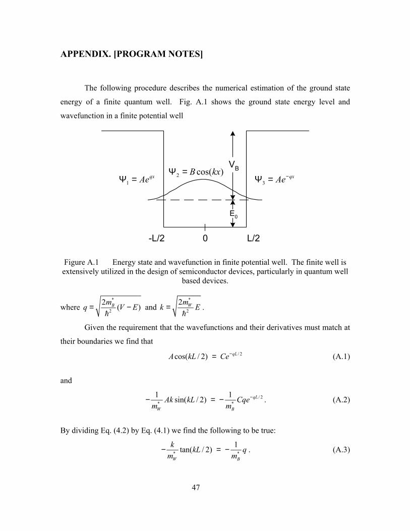
APPENDIX. [PROGRAM NOTES]
The following procedure describes the numerical estimation of the ground state
energy of a finite quantum well. Fig. A.1 shows the ground state energy level and
wavefunction in a finite potential well
0-L/2 L/2
E0
VB
1qxAeΨ = 2 cos( )B kxΨ =
3qxAe−Ψ =
Figure A.1 Energy state and wavefunction in finite potential well. The finite well is extensively utilized in the design of semiconductor devices, particularly in quantum well
based devices.
where *
2
2 (Bmq V= − )E and *
2
2 Wmk E= .
Given the requirement that the wavefunctions and their derivatives must match at
their boundaries we find that
(A.1) / 2cos( / 2) qLA kL Ce−=
and
/ 2*
1 1sin( / 2) qL
W B
Ak kL Cqem m
−− = − * . (A.2)
By dividing Eq. (4.2) by Eq. (4.1) we find the following to be true:
*
1tan( / 2)W B
k kL qm m
− = *− . (A.3)
47

After substitution (for k and q in terms of energy) and simplification we find that the
ground state energy must satisfy
* 2
* 2
(tan2W
W B
m LE Em m
−= *
)V E (A.4)
Since the value of V is unknown, we begin with the maximum possible value (as
discussed in the text) and cyclically narrow down the value of the offset until it converges
on the actual value. We have created the following program in Matlab to calculate the
conduction band offset and ground state energy for a given VB. Parameters for any
rectangular quantum well can be used as inputs for the calculation of the offset.
clc clear all Vb = 0.2254; %[eV] m_e = 9.11e-31; %[kg] hbar = 1.055e-34; %[J*s] Eapprox(1) = 0.492; %[eV] L = 3.6e-9; %[m] J = L/2; %[m] q = 1.602e-19; %[C] m_effw = 0.059*m_e; %[kg] m_effb = 0.084*m_e; %[kg] Vapprox(1) = Eapprox(1) + Vb; for n = 2:1:10000 a = 1; y = 0; for E = 0.001:0.001:Vapprox(n-1); AA = sqrt((E*q)/m_effw); AB = sqrt((2*m_effw*E*q*(J^2))/(hbar^2)); AC = sqrt(((Vapprox(n-1) - E)*q)/m_effb); P = AA*tan(AB) - AC; z = y; y = P; if z.*y < 0 Eout(a) = E; a = a+1; end end Eapprox(n) = Eout(1); Vapprox(n) = Eapprox(n) + Vb; if Vapprox(n) == Vapprox(n-1) disp(Vapprox(n))
48

break end
end
49

THIS PAGE INTENTIONALLY LEFT BLANK
50

INITIAL DISTRIBUTION LIST
1. Defense Technical Information Center Ft. Belvoir, Virginia
2. Dudley Knox Library Naval Postgraduate School Monterey, California
3. Chairman (Code PH) Department of Physics
Naval Postgraduate School Monterey, California
4. Gamani Karunasiri Naval Postgraduate School Monterey, California
5. James Luscombe Naval Postgraduate School Monterey, California
6. Ensign Thomas R. Hickey United States Navy 73 Greenbush Street Cortland, New York
51


![SIGNATURE SERIES Operational Amplifiers · 2019. 3. 1. · 25℃ 27 - - 27 28 - + V Vcc =30[V],RL=10[kΩ] 99 Full range 27 28 - 27 - - Vcc+=30[V],RL=10[kΩ] Low Level](https://img.pdfslide.us/doc/110x75/610890e11c5c5355b33d8b3e/signature-series-operational-2019-3-1-25af-27-i-i-27-28-i-v-vcc-30vrl10k.jpg)


![UK BS 7671 16 VDE 0100 EN-60601/60335/60950/61010 VDE …download.flukecal.com/pub/literature/Fluke... · 2 [1] 50 kΩ 60 kΩ 100 kΩ / 20 V 500,000 8 10 kΩ 10 GΩ 4.5 CE Low Voltage](https://img.pdfslide.us/doc/110x75/5e7807e35be0b42eba4126eb/uk-bs-7671-16-vde-0100-en-60601603356095061010-vde-2-1-50-k-60-k-100-k.jpg)