Embed Size (px)
Citation preview

Thermionic Emission and Negative dI/dVin Photoactive Graphene Heterostructures
The MIT Faculty has made this article openly available. Please share how this access benefits you. Your story matters.
Citation Rodriguez-Nieva, Joaquin F., Mildred S. Dresselhaus, and Leonid S.Levitov. “Thermionic Emission and Negative D I /D V in PhotoactiveGraphene Heterostructures.” Nano Letters 15.3 (2015): 1451–1456.
As Published http://dx.doi.org/10.1021/nl502522q
Publisher American Chemical Society (ACS)
Version Author's final manuscript
Citable link http://hdl.handle.net/1721.1/110518
Terms of Use Article is made available in accordance with the publisher'spolicy and may be subject to US copyright law. Please refer to thepublisher's site for terms of use.

Thermionic Emission and Negative dI/dV in Photoactive Graphene Heterostructures
J. F. Rodriguez-Nieva1, M. S. Dresselhaus1,2, L. S. Levitov1
1Department of Physics, Massachusetts Institute of Technology, Cambridge, MA 02139, USA and2Department of Electrical Engineering and Computer Science,
Massachusetts Institute of Technology, Cambridge, MA 02139, USA(Dated: April 15, 2015)
Transport in photoactive graphene heterostructures, originating from the dynamics of photogen-erated hot carriers, is governed by the processes of thermionic emission, electron-lattice thermalimbalance and cooling. These processes give rise to interesting photoresponse effects, in particu-lar negative differential resistance (NDR) arising in the hot-carrier regime. The NDR effect stemsfrom a strong dependence of electron-lattice cooling on the carrier density, which results in thecarrier temperature dropping precipitously upon increasing bias. The ON-OFF switching betweenthe NDR regime and the conventional cold emission regime, as well as the gate-controlled closed-circuit current that is present at zero bias voltage, can serve as signatures of hot-carrier dominatedtransport.
Graphene, because of its unique characteristics, is ofkeen interest for optoelectronics research in areas such asphotodetection, solar cells and light-emitting devices [1–4]. Recently it was emphasized that graphene features anunusual kind of photoresponse mediated by photogener-ated hot carriers. The hot-carrier regime originates fromthe quenching of electron-lattice cooling when the systemis close to charge-neutrality [5, 6]. The hot carriers areexceptionally long-lived in graphene and can proliferateacross the entire system [7–9]. This behavior, which setsgraphene apart from other photoactive materials, leadsto a dramatic enhancement in photo-response.
The 2D character of electronic states, which are fullyexposed in materials such as graphene, can enable newdevice architectures. One system of high current in-terest is stacked graphene-dielectric-graphene structures[see Fig.1(a)]. Fabricated with atomic precision, such sys-tems can behave as field-effect transistors [10, 11], reso-nant tunnel diodes [12, 13], photodetectors [14, 15]; theyalso provide a platform to explore the Coulomb Drag ef-fect [16] and the metal-insulator transition [17]. In thehot-carrier regime, proliferation of photoexcited electron-hole pairs can result in an enhanced thermionic emissionof hot carriers over the barrier. Vertical carrier extractionin such structures is facilitated by short interlayer trans-port lengths in the nanometer range, ultra-fast responsetimes, and large active areas. Variability in properties ofdifferent 2D barrier materials (hBN, MoS2, WSe2, etc.)allows to tailor the photo-response characteristics to thedifferent optoelectronic applications.
Here we predict that interlayer transport in grapheneheterostructures operating in the hot-carrier regime leadsto an unusual type of photoresponse, namely, a neg-ative differential resistance (NDR). The mechanism ofthis NDR response relies on the interplay of two effects.First, the phase space available for phonon scatteringrapidly increases with doping, enhancing the electron-lattice cooling and thereby altering the number of hotcarriers in the system. Second, the large capacitance of
the atomically thin device renders the carrier density ingraphene layers sensitive to the interlayer potential dif-ference. These two effects combined together result in areduction of the electronic temperature and a suppres-sion of thermionic current upon an increase of the biaspotential Vb. The NDR effect arises when this suppres-sion overwhelms the increase in the field-effect transportunder bias. Such an NDR mechanism manifests itselfas an enhanced photo-current peaked at a bias potentialwell below the onset of the conventional field-emissionregime, eVb ∆, where ∆ is the barrier height, as shownin Fig.1(c).
We note that the photoactive NDR architectures are aclass of their own, and are well suited for optoelectronicapplications. In particular, the fast response and in-situtunability of graphene devices makes them ideal as photo-active switches or light-detectors with high gain. TheNDR effect in photo-active devices, analyzed below, isdistinct from the one in traditional NDR devices, suchas Gunn diodes [18] or resonant tunneling diodes [19,20] which rely on non-linearities under the application oflarge electric fields in the absence of light.
Turning to the technical discussion, we note that, whilein general both electrons and holes can contribute tothermionic transport, in practice transport is often dom-inated by a single carrier type. In the case of hBN, thebarrier heights are ∆el ∼ 3.5 eV for electron transportand ∆h ∼ 1.3 eV for hole transport [21]. We can thereforetreat the interlayer transport in an hBN-based system asdominated by a single carrier type (holes).
Below we focus on the behavior in wide-barrier struc-tures, where thermionic emission of thermally activatedcarriers dominates over direct tunneling. This is the casefor hBN thicknesses exceeding 4-5 monolayers (d ∼ 1 nm)[11] at sufficiently high temperatures. Thermionic cur-rents are described by a particularly simple model whenboth graphene layers are at neutrality at Vb = 0[22]:
J (Vb, T ) = (g0/eβ)e−β∆ sinh(βeVb/2), (1)
arX
iv:1
501.
0692
7v2
[co
nd-m
at.m
es-h
all]
14
Apr
201
5

2
FIG. 1. The Negative Differential Resistance (NDR) effectin a photoactive heterostructure operated in the thermionicemission regime. Shown here are (a) device schematics, (b)electronic band structure with the quantities discussed in thetext marked, and (c) the I − V dependence under opticalpumping obtained from Eqs. (4)–(7). The bias voltage Vb
controls the electron cooling through electrostatic doping ofgraphene layers. An enhancement in the cooling power uponincreased Vb triggers carrier temperature dropping [marked
T (1,2,3) in (c)]; see also simulation results in Fig.4(a). Theresulting suppression of thermionic current leads to negativedI/dV (in the grey region). For larger bias values, transport isdominated by field emission, yielding positive dI/dV outsidethe grey region. Shown here are results for both graphenelayers undoped at Vb = 0. Results for nonzero doping arepresented in Figs.2,3.
where J is the current density per unit area, β−1 = kBTand the g0 value is estimated in Eq.(8). This expressionfollows from a general microscopic model at not too highbias Vb, such that the effect of anti-symmetric dopinginduced by Vb 6= 0 is stronger than the correspondingchange in the barrier skewness [see derivation and dis-cussion in the paragraph before Eq.(11)]. For larger biasvalues, field corrections to the barrier potential becomeimportant and must be accounted for; this is done in amicroscopic model developed below. We also note thatthe electronic distribution is typically non-exponentialwhen relaxation is slow. Slow relaxation would make thedistribution tails more pronounced, ultimately enhancingthe thermionic effects.
The steep dependence of J on T and Vb in Eq.(1)
FIG. 2. The closed-circuit current Jcc induced by opticalpumping (P = 10µW/µm2) in the absence of voltage bias,Vb = 0. In the transport regime dominated by hot carriers,the value and polarity of Jcc are sensitive to the carrier den-sities n1, n2 in the graphene layers. Shown are experimentalschematics (a), and the dependence Jcc vs. n1 and n2 (b).The four-fold pattern with multiple changes of the currentpolarity arises due to the strong cooling power dependenceon carrier concentration (a non-linear color scale is used toamplify the features of interest).
leads to NDR by the following mechanism. For electronsin thermal equilibrium with the lattice, Eq. (1) predictsa monotonic I − V dependence. A very different be-havior, which is key for NDR, arises under pumping.As pictured schematically in Fig.1(c) for three valuesT (1) > T (2) > T (3), in the hot-carrier regime the elec-tron temperature T becomes highly sensitive to Vb. Thetemperature-bias coupling arises because of the large in-terlayer capacitance producing bias-dependent doping inthe graphene layers. An increase in carrier density leadsto a faster electron-lattice cooling, which reduces thermalimbalance ∆T = T−T0, with T0 the lattice temperature.The dependence in Eq.(1) then predicts suppression ofthermionic emission. If strong enough, this suppressioncan lead to negative dI/dV . The NDR effect takes placein the grey region marked in Fig.1(c).
The sensitivity of the electron-lattice cooling to car-rier concentration provides a smoking gun for the regimedominated by hot carriers, helping distinguish it from theconventional resonant tunneling NDR mechanisms, suchas those discussed in Refs. [12, 13]. In that regard, wemention that for the more general case of unequal car-rier densities (n1 6= n2 at Vb = 0), our analysis predictsthat the interlayer thermionic transport persists even atzero bias. As illustrated in Fig.2, this produces a closed-circuit current at Vb = 0 with a characteristic densitydependence: a four-fold pattern with multiple polaritychanges. Such a pattern provides a characteristic signa-ture of hot-carrier dominated transport.
The strength of the hot-carrier effects, reflected in theresponse of T to Vb [see Fig.4(a)], can be characterizedby the dimensionless quantity
α = −∆
T
dT
d(eVb). (2)

3
The value α depends mainly on the power P pumped intothe electronic system and on the thickness d of the barriervia the capacitance effect. As we will see, α governs theN-shaped I − V dependence: the condition for NDR canbe stated as α > 1/2. We will argue that values as largeas α ∼ 25 can be reached under realistic conditions.
We now proceed to introduce our transport model. Forthermionic transport over the barrier, as well as for tun-neling through it, we adopt a quasi-elastic but momen-tum non-conserving approximation. Indeed, a numberof momentum scattering mechanisms at the interface arepossible, such as scattering by defects, intrinsic phonons,substrate phonons, etc. Typical energy exchange in theseprocesses is small on the barrier height scale ∆. With thisin mind, we use the (quasi-elastic) WKB model for theinterlayer transition matrix element:
t(ε) = Γe−1h
∫ x∗0
p(x)dx,p2(x)
2m= ∆− eEbx− ε, (3)
for ε < ∆, and t(ε) = Γ for ε > ∆, where Γ is an energy-independent prefactor which depends on the barrier ma-terial properties. In Eq. (3), Eb is the electric field withinthe barrier due to interlayer bias, see Eq.(7), m is theelectron effective mass in the dielectric, and x∗ is theclassical turning point for the skewed barrier potential,x∗ = min[d, (∆ − ε)/eEb], see Fig. 1(b). Here, for thesake of simplicity, we ignore the effect of attraction to im-age charges, described by a −1/|x| − 1/|x− d| potential.For a large barrier width, this gives rise to the barrierheight Schottky dependence on the square root of Eb.The effect is less dramatic for the not-so-large barrierwidths analyzed below.
Assuming an elastic but momentum non-conservinginterlayer transport, the vertical current J (Vb) canbe expressed through barrier transmission and carrierdistribution[23]:
J (Vb) = e∑ε,ij
2π
h|tij(ε)|2D1(ε)D2(ε)[f1(ε)− f2(ε)], (4)
where, due to the built-in field between layers, the en-ergy for the quantities in layer 2 is offset by ε = ε+ eEbd[see Fig.1(b)]. Here J is the current per unit area,f1(ε) = [eβ1(ε−µ1) + 1]−1, f2(ε) = [eβ2(ε−µ2) + 1]−1 arethe Fermi distribution functions, the sum denotes inte-gration over ε and summation over spins and valleys.We use tij(ε) = δijt(ε) defined in Eq.(3), and the den-sity of states per spin/valley D1,2(ε) = |ε|/2π(hv)2 withv ≈ 106 m/s the carrier velocity. The temperatures es-tablished under pumping in unequally doped layers aregenerally distinct, β1 6= β2, reflecting the cooling ratesdensity dependence. Also, importantly, the electrostaticpotential between layers, Ebd, is distinct from the biasvoltage Vb. This is so because the quantum capacitanceeffects, prominent at small carrier densities,[24] make thequantites µ1 and µ2 bias-dependent. These effects will beinvestigated below.
A feature of our system which is key for NDR is thelarge mutual capacitance of graphene layers, which cou-ples Vb with the carrier density and makes the hot-carrierproperties of each layer tunable. This coupling acts as aknob producing big changes in the hot-carrier photore-sponse through modest changes of carrier concentrationon the order δn ∼ 1012 cm−2. Such bias-induced dopingchanges are routine in graphene/hBN systems [10].
The bias-induced changes in carrier densities ofgraphene layers, as well as the electric field Eb betweenthe layers, can be described by a simple electrostaticmodel. We consider a dual-gated device with fixed chargedensities nT, nB in the top and bottom gates, respec-tively. The neutrality condition relates the charge densi-ties in the different regions of the device as
nT + n1 + n2 + nB = 0, (5)
where n1, n2 are carrier densities on the graphene layers.The field Eb is related to these quantities through Gauss’law:
κEb = 2πe (nT + n1 − n2 − nB), (6)
where κ is the dielectric constant of the barrier. A biasvoltage Vb applied between the graphene layers results in
eVb = µ1 − µ2 + eEbd. (7)
With doping-dependent µ1,2, Eq.(7) accounts for thequantum capacitance effects. Here we will use the T = 0expression µi = sign(ni)hv
√π|ni|, which provides a good
model over most of the relevant carrier density range.The three unknown variables n1, n2 and Eb can now
be found by solving the three equations (5)-(7), once theexternal variables nT, nB and Vb are fixed. Through-out this work we focus on the symmetric case whennT = nB = −n0 with no interlayer bias applied (whichcorresponds to both graphene layers at neutrality whenthe gates are uncharged). In this case, Eqs. (5),(6) can berestated as n1 = n0+δn, n2 = n0−δn, and κEb = 4πeδn.Then, plugging these values into Eq. (7), the density im-balance δn can be obtained. The built-in field Eb mattersin two different ways: the electrostatic potential valueeEbd enters the WKB model, Eq. (3), as well as in theoffset between D1(ε) and D2(ε) in Eq. (4).
The I − V dependence for the case n0 = 0 in shownin Fig.1; for finite values nT = nB = −n0 it is shownin Fig.3. In our simulation, we first determine µ1,2 fromEqs.(5)-(7) as a function of Vb and n0. Using the µ1,2
values, the electronic temperatures T1,2 are determinedfrom energy balance considerations, see Eq.(9) below. Fi-nally, using the calculated values µ1,2, T1,2, and Eb, thecurrent is obtained from Eq.(4). We use hBN barrier pa-rameters for numerical estimates, with a (hole) barrierheight ∆ ∼ 1.3 eV [21], dielectric constant κ ∼ 5, thick-ness d = 6 nm (∼ 20 monolayers). Room temperature isassumed, T0 = 300 K, unless stated otherwise.
4
The prefactor value Γ in Eq.(3) can be related tothe measured conductance. Physically, Γ accounts forthe processes in which tunneling couples to phonons ordefects. The rates for these processes, which typicallyvary from interface to interface, can be estimated fromtransport measurements. Linearizing Eq.(4) in eVb forkBT ∆, and accounting for the thermionic contribu-tion due to ε ≈ ∆, the zero-bias conductance per unitarea is
G =g0
2e−β∆, g0 = 4πND1(∆)D2(∆)|Γ|2 e
2
h, (8)
where we take T1 = T2. Here N = 4 is the spin/valleydegeneracy, and g0 is a prefactor in Eq. (1). Theactivation T dependence is consistent with that mea-sured for dark current [25]. Comparison with valuesG ∼ 10−7 Ω−1µm−2 measured at room temperature, and∆ ∼ 0.4 eV [25], yields values g0 ∼ 1 Ω−1µm−2 andΓ ∼ 0.5 eVA.
Next we discuss how hot-carrier effects result in a cou-pling between the electronic temperature and the chem-ical potential for each graphene layer. In the contin-uous wave regime, the power P pumped into the elec-tronic system is distributed among the electron and lat-tice degrees of freedom. For simplicity, we will use a two-temperature model, describing electrons by a tempera-ture distinct from the lattice temperature, T > T0, validwhen the carrier-carrier scattering rate is faster than theelectron-lattice relaxation rate. Assuming spatially uni-form in-plane temperatures and chemical potentials, thetotal cooling power P obeys the energy balance condition
P = Pac(µi, Ti) + Popt(µi, Ti) + Pdis(µi, Ti), (9)
written separately for each layer i = 1, 2. Here we ignoredeffects such as direct interlayer energy transfer as wellas the heat drained through the contacts. Equation (9)accounts for three cooling pathways intrinsic to graphene,mediated by acoustic and optical phonons (Pac, Popt) [5,6], and the disorder-assisted acoustic phonon mechanism(Pdis) [26], see Supplement. The cooling rates in Eq.(9)also depend on the lattice temperature T0, however itsuffices to treat T0 as a fixed parameter, since the heatcapacity of the lattice greatly exceeds that of the electronsystem.
The intralayer Joule heating is small and thus neednot be included in Eq. (9). Indeed, typical vertical cur-rent values obtained in devices of active area∼ 1µm2 andunder a bias Vb ∼ 1 V do not exceed a few nA [10, 11, 25].This yields Joule heating sources which are at least threeorders of magnitude smaller than the powers pumped op-tically. The interlayer energy transfer as well as the heatdrained through contacts can be ignored in the energybalance in Eq. (9) for similar reasons.
The cooling power is a strong function of doping forthe acoustic-phonon contributions Pac and Pdis. This is
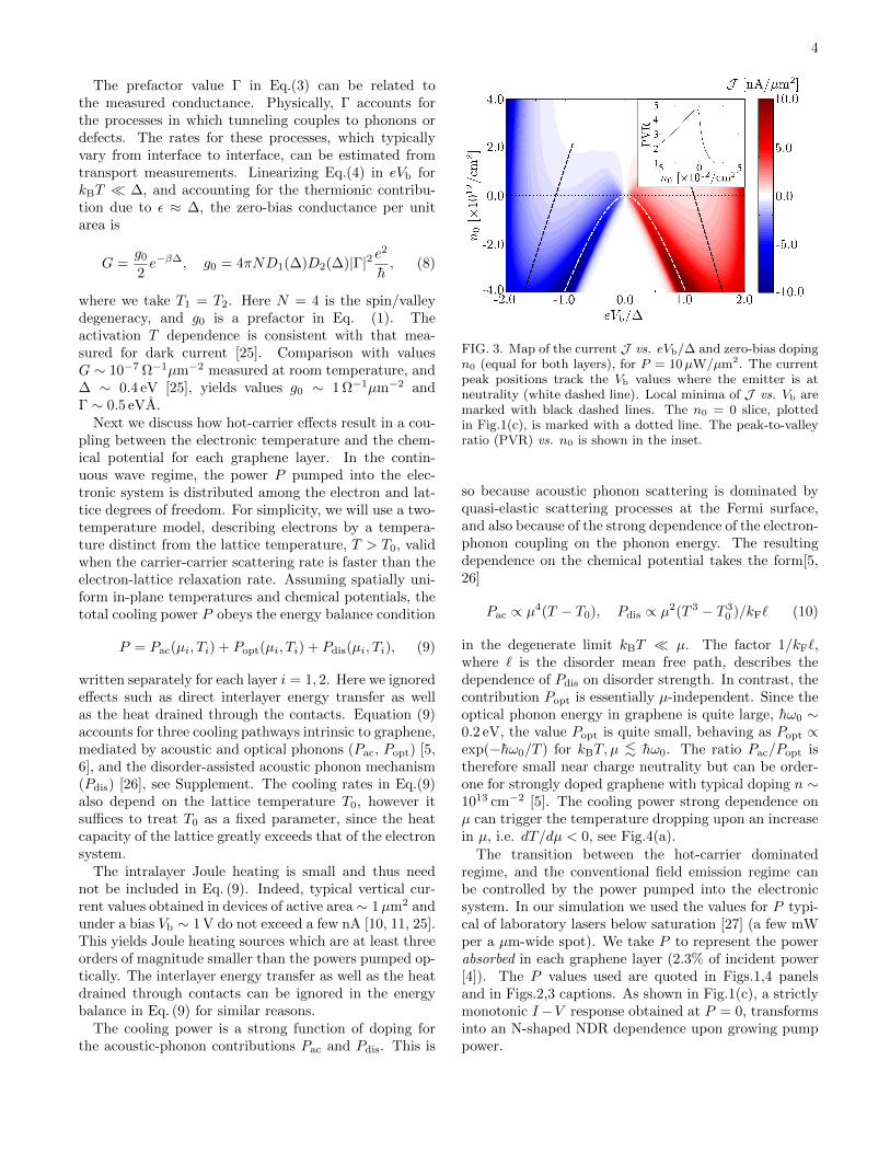
FIG. 3. Map of the current J vs. eVb/∆ and zero-bias dopingn0 (equal for both layers), for P = 10µW/µm2. The currentpeak positions track the Vb values where the emitter is atneutrality (white dashed line). Local minima of J vs. Vb aremarked with black dashed lines. The n0 = 0 slice, plottedin Fig.1(c), is marked with a dotted line. The peak-to-valleyratio (PVR) vs. n0 is shown in the inset.
so because acoustic phonon scattering is dominated byquasi-elastic scattering processes at the Fermi surface,and also because of the strong dependence of the electron-phonon coupling on the phonon energy. The resultingdependence on the chemical potential takes the form[5,26]
Pac ∝ µ4(T − T0), Pdis ∝ µ2(T 3 − T 30 )/kF` (10)
in the degenerate limit kBT µ. The factor 1/kF`,where ` is the disorder mean free path, describes thedependence of Pdis on disorder strength. In contrast, thecontribution Popt is essentially µ-independent. Since theoptical phonon energy in graphene is quite large, hω0 ∼0.2 eV, the value Popt is quite small, behaving as Popt ∝exp(−hω0/T ) for kBT, µ <∼ hω0. The ratio Pac/Popt istherefore small near charge neutrality but can be order-one for strongly doped graphene with typical doping n ∼1013 cm−2 [5]. The cooling power strong dependence onµ can trigger the temperature dropping upon an increasein µ, i.e. dT/dµ < 0, see Fig.4(a).
The transition between the hot-carrier dominatedregime, and the conventional field emission regime canbe controlled by the power pumped into the electronicsystem. In our simulation we used the values for P typi-cal of laboratory lasers below saturation [27] (a few mWper a µm-wide spot). We take P to represent the powerabsorbed in each graphene layer (2.3% of incident power[4]). The P values used are quoted in Figs.1,4 panelsand in Figs.2,3 captions. As shown in Fig.1(c), a strictlymonotonic I−V response obtained at P = 0, transformsinto an N-shaped NDR dependence upon growing pumppower.
5
The impact of doping n0 (taken to be equal for bothlayers at Vb = 0) on the I − V dependence is illustratedin Fig.3. The current peaks are shifted towards higherVb values upon n0 growing more negative [compare toFig.1(c) which shows the n0 = 0 slice]. The peaks trackthe Vb values at which the emitter layer is bias-dopedto charge neutrality. This is to be expected since theelectron-lattice imbalance is maximal at neutrality. Thepeak-to-valley ratio (PVR) as high as ∼ 5 can be ob-tained (see Fig. 3 inset). For n0 > 0, in contrast, theemitter layer is never at charge neutrality for any valueof Vb, resulting in the N-shaped dependence fading out.
The NDR effect is suppressed under a high bias poten-tial when field emission of carriers with energies belowthe barrier height overwhelms thermionic emission. Asshown in Fig.1, the high bias region eVb/∆ > 1 is charac-terized by J monotonically growing with increasing Vb.This behavior arises because lowering the barrier facili-tates tunneling and also because growing carrier densityresults in a faster cooling, thereby reducing the electron-lattice thermal imbalance [see Fig.1(c) inset].
Next, we proceed to derive a simple criterion for NDR.We will focus on the fully-neutral case n0 = 0 (bothgraphene layers undoped at Vb = 0) pictured in Fig.1.In this case, due to symmetry, we have T1 = T2 = Tand n1 = −n2 for any eVb. Further, assuming a smallbias and/or a not-too-wide barrier, we can approximatethe bias-induced chemical potentials as µ1,2 ≈ ±eVb/2.This simple relation is valid for eVb κ(hv)2/e2d, cor-responding to the last term in Eq.(7) much smaller thanµ1 − µ2. Lastly, accounting for the dominant role ofthermionic emission, we model transmission as a stepfunction, |t(ε)|2 ≈ Γ2θ(ε − ∆). We integrate in Eq. (4)over energies ε ≥ ∆ max[kBT, Vb], approximatingD1,2(ε) as a constant and the Fermi distribution tail ase−β(ε−µ). This yields Eq.(1) to leading order in Vb/∆and kBT/∆ with the prefactor g0 given in Eq.(8). Whilethe validity of Eq.(1) is limited to d which are not toosmall and also not too large, we find that it predicts NDRin the parameter range close to that found from the fullmicroscopic model used to produce Figs.1–4.
The criterion for NDR can be derived by taking thederivative dJ /dVb in Eq. (1) and setting it to zero, giving(
1 +1
β∆
)tanhx− x
β∆=
1
2α, x = βeVb/2, (11)
where α is the quantity −(∆/eT )dT/dVb introducedabove, describing the carrier temperature dependence vs.Vb. The α value controls the NDR effect. Maximizingthe left-hand side in x we find the value f(λ) = λ1/2 −(λ−1) tanh−1 λ−1/2 parameterized with λ = 1+(β∆)−1,which is attained at x∗ = sinh−1√β∆. It is straightfor-ward to check that f(λ) ≤ 1 for all λ ≥ 1. This gives theNDR condition α > 1/2. Below we use this condition,derived for n0 = 0, as an approximation for the moregeneral case of n0 6= 0.
To estimate α as a function of the model parameters,it is convenient to factorize α by applying the chain ruleas α = αT · αµ, giving
αT (P ) = −µT
dT
dµ, αµ(d) =
∆
eµ
dµ
dVb. (12)
Here αT depends only on the cooling pathways throughEq. (9), while αµ depends only on the barrier propertiesthrough the quantum capacitance effect of Eq. (7). Belowwe use Eq.(12) to estimate α and show that the NDRcondition α > 1/2 can be readily met.
To estimate αT we analyze the degenerate regime µkBT , where the doping-dependent contributions Pac andPdis dominate over the roughly doping-independent Popt
[see Fig.4(a) inset]. In this regime, the cooling powerbehaves as Pi = γiµ
a(T b − T b0 ), with a = 4, b = 1 foracoustic phonon cooling, and a = 2, b = 3 for disorder-assisted cooling (here γi are constants that depend onthe cooling pathways, see Supplement). We assume, forsimplicity, that a single cooling pathway dominates overother pathways. Then Eq. (9) yields
αT = (a/b)[1− (T0/T )b] (13)
This gives 0 < αT < a/b with the low and high val-ues corresponding to T ≈ T0 and T T0, respectively.The crossover between these values occurs at a thresholdpump power P∗ ∼ 0.5µW/µm2 that marks the onset ofthe hot-carrier regime under typical experimental condi-tions. We define P∗ as the value for P at typical carrierdensities n ∼ 1012 cm−2, T0 = 300 K, and kF` = 100 suchthat (T − T0)/T0 = 0.1. This yields the above P∗ value.Maximum αT values found from Eq.(13) are 0.6 and 4for the Pdis and Pac pathways, respectively.
Next, we estimate αµ as a function of the barrier width.From Eq. (7), specializing to the case n0 = 0, we find
αµ =∆/2µ
1 + (4e2/κhv)kFd∼ 6.5
1 + 0.3 d[nm]. (14)
where kF = µ/hv. Here we have used the hBN barriervalue ∆ ∼ 1.3 eV and µ ∼ 0.1 eV for typical bias-induceddoping. This gives limiting values αµ(d d∗) ≈ 6.5 andαµ(d d∗) = 0, with the crossover value d∗ ∼ 20 nm.From the above we see that the quantity α = αT ·αµ canreach values as high as α ∼ 25.
While the NDR criterion α > 1/2 is insensitive tothe cooling mechanism (so long as it is a strong func-tion of carrier density, as discussed above), the form ofthe I − V dependence may reflect the cooling mecha-nism specifics. This is illustrated in Fig.4(b) for thePdis mechanism. In particular, we consider the bias Vpk
where the current peaks. From Eq. (11) we estimateeVpk ≈ x∗kBT . When the Pdis mechanism dominates(kF` < 103) and T T0, a power-law relation is ob-
tained: Vpk ∝[kF` P/µ
2]1/3
. Similar arguments lead

6
FIG. 4. (a) Electronic temperature T vs. bias Vb for differentpump power values P . The inset shows the dominant cool-ing pathways for different chemical potential and pump powervalues [for T0 = 0 K, kF` = 100]. (b) Current J vs. Vb fordifferent kF` values, and P = 10µW/µm2. The bias poten-tial at which current peaks (Vpk) and the peak-to-valley ratio(PVR) are sensitive to the amounts of disorder (see inset).Results shown in this figure (except the inset of panel a) areobtained for the system undoped at Vb = 0, as in Fig.1.
to a disorder-controlled peak-to-valley ratio (PVR). Thisbehavior is illustrated in Fig.4(b) inset.
We note that the NDR features may be somewhatsmeared out by statistical fluctuations induced by disor-der or inhomogeneities. However, we do not expect theseeffects to destroy NDR. Indeed, optical heating occurs inµm-wide areas and a typical carrier density is 1012 cm−2.At the same time, charge inhomogeneity lengthscales ingraphene/hBN are a few tens of nm, whereas typical den-sity fluctuations are as low as ∼ 1011 cm−2 [28, 29].
Summing up, vertically-stacked graphene heterostruc-tures afford a platform to realize and explore a range ofinteresting optoelectronic phenomena due to photogen-erated hot carriers. One such phenomenon is the light-induced NDR effect discussed above, manifesting itselfthrough the I − V dependence, acquiring an N-shapedcharacter under optical pumping. Vertical heterostruc-tures use the full graphene area as a photoactive region,and possess a large degree of tunability. These proper-
ties make the NDR effect potentially useful for design-ing new types of optical switches and photodetectors.Our estimates show that the NDR regime, facilitated bygraphene’s unique optical and thermal properties, can bereadily accessed in wide-barrier heterostructures.
ACKNOWLEDGMENTS
We thank N. Gabor and J. C. W. Song for usefuldiscussions. This work was supported as part of theCenter for Excitonics, an Energy Frontier Research Cen-ter funded by the U.S. Department of Energy, Office ofScience, Basic Energy Sciences under Award No. de-sc0001088 (LL), and by the National Science FoundationGrant NSF/DMR1004147 (JFRN and MSD).
[1] Bonaccorso, F.; Sun, Z.; Hasan, T.; Ferrari, A. C. NatPhoton 2010, 4, 611
[2] Bao, Q.; Loh, K. P. ACS Nano 2012, 6, 3677–3694[3] Xia, F.; Mueller, T.; Lin, Y.-m.; Valdes-Garcia, A.;
Avouris, P. Nat Nano 2009, 4, 839–843[4] Nair, R. R.; Blake, P.; Grigorenko, A. N.;
Novoselov, K. S.; Booth, T. J.; Stauber, T.; Peres, N.M. R.; Geim, A. K. Science 2008, 320, 1308
[5] Bistritzer, R.; MacDonald, A. H. Phys. Rev. Lett. 2009,102, 206410
[6] Tse, W.-K.; Das Sarma, S. Phys. Rev. B 2009, 79,235406
[7] Xu, X.; Gabor, N. M.; Alden, J. S.; van der Zande, A. M.;McEuen, P. L. Nano Lett. 2010, 10, 562-566
[8] Lemme, M. C.; Koppens, F. H. L.; Falk, A. L.; Rud-ner, M. S.; Park, H.; Levitov, L. S.; Marcus, C. M., NanoLett. 2011, 11, 4134-4137
[9] Gabor, N. M.; Song, J. C. W.; Ma, Q.; Nair, N. L.;Taychatanapat, T.; Watanabe, K.; Taniguchi, T.; Levi-tov, L. S.; Jarillo-Herrero, P. Science 2011, 334, 648-652
[10] Britnell, L.; Gorbachev, R. V.; Jalil, R.; Belle, B. D.;Schedin, F.; Mishchenko, A.; Georgiou, T.; Katsnel-son, M. I.; Eaves, L.; Morozov, S. V.; Peres, N.M. R.; Leist, J.; Geim, A. K.; Novoselov, K. S.; Pono-marenko, L. A. Science 2012, 335, 947–950
[11] Britnell, L.; Gorbachev, R. V.; Jalil, R.; Belle, B. D.;Schedin, F.; Katsnelson, M. I.; Eaves, L.; Moro-zov, S. V.; Mayorov, A. S.; Peres, N. M. R.; Cas-tro Neto, A. H.; Leist, J.; Geim, A. K.; Pono-marenko, L. A.; Novoselov, K. S. Nano Letters 2012,12, 1707–1710
[12] Britnell, L.; Gorbachev, R. V.; Geim, A. K.; Pono-marenko, L. A.; Mishchenko, A.; Greenaway, M. T.;Fromhold, T. M.; Novoselov, K. S.; Eaves, L. Nat Com-mun 2013, 4,1794
[13] Mishchenko, A.; Tu, J. S.; Cao, Y.; Gorbachev, R. V.;Wallbank, J. R.; Greenaway, M. T.; Morozov, V. E.;Morozov, S. V.; Zhu, M. J.; Wong, S. L.; Withers, F.;Woods, C. R.; Kim, Y-J.; Watanabe, K.; Taniguchi, T.;Vdovin, E. E.; Makarovsky, O.; Fromhold, T. M.;

7
Fal’ko, V. I.; Geim, A. K.; Eaves, L.; Novoselov, K. S.;Nat Nano 2014, 9, 808
[14] Britnell, L.; Ribeiro, R. M.; Eckmann, A.; Jalil, R.;Belle, B. D.; Mishchenko, A.; Kim, Y.-J.; Gor-bachev, R. V.; Georgiou, T.; Morozov, S. V.; Grig-orenko, A. N.; Geim, A. K.; Casiraghi, C.; Neto, A. H. C.;Novoselov, K. S. Science 2013, 340, 1311–1314
[15] Yu, W. J.; Liu, Y.; Zhou, H.; Yin, A.; Li, Z.; Huang, Y.;Duan, X. Nat Nano 2013, 8, 952
[16] Gorbachev, R. V.; Geim, A. K.; Katsnelson, M. I.;Novoselov, K. S.; Tudorovskiy, T.; Grigorieva, I. V.;MacDonald, A. H.; Morozov, S. V.; Watanabe, K.;Taniguchi, T.; Ponomarenko, L. A. Nat Phys 2012, 8,896–901
[17] Ponomarenko, L. A.; Geim, A. K.; Zhukov, A. A.;Jalil, R.; Morozov, S. V.; Novoselov, K. S.; Grig-orieva, I. V.; Hill, E. H.; Cheianov, V. V.; Fal’ko, V. I.;Watanabe, K.; Taniguchi, T.; Gorbachev, R. V. Nat Phys2011, 7, 958
[18] Butcher, P. N. Reports on Progress in Physics 1967, 30,97
[19] Tsu, R.; Esaki, L. Applied Physics Letters 1973, 22, 562–564
[20] Sollner, T. C. L. G.; Goodhue, W. D.; Tannenwald, P. E.;Parker, C. D.; Peck, D. D. Applied Physics Letters 1983,43, 588–590
[21] Kharche, N.; Nayak, S. K. Nano Letters 2011, 11, 5274–5278
[22] Our expression for thermionic current density, Eq.(1),features a dependence on the external bias and a power-law temperature dependence distinct from that knownfor the 3D case, where Jth ∝ T 2e−∆/kBT . This reflectsthe difference in the transport processes at the interface.Conventional thermionic emission (3D) is described asthe flux of free particles with energies ε > ∆ in the di-rection normal to the surface. In contrast, in our casetransport depends on elastic scattering mechanisms atthe graphene/hBN interface generating an out-of-planecurrent, as described in the text.
[23] Wolf, E. L. Principles of electron tunneling spectroscopy,Second Edition; Oxford University Press: New York,2012.
[24] Luryi, S. Appl. Phys. Lett. 1988, 52, 501–503[25] Georgiou, T.; Jalil, R.; Belle, B. D.; Britnell, L.; Gor-
bachev, R. V.; Morozov, S. V.; Kim, Y.-J.; Gholinia, A.;Haigh, S. J.; Makarovsky, O.; Eaves, L.; Pono-marenko, L. A.; Geim, A. K.; Novoselov, K. S.;Mishchenko, A. Nat Nano 2013, 8, 100–103
[26] Song, J. C. W.; Reizer, M. Y.; Levitov, L. S. Phys. Rev.Lett. 2012, 109, 106602
[27] Sun, Z.; Hasan, T.; Torrisi, F.; Popa, D.; Privitera, G.;Wang, F.; Bonaccorso, F.; Basko, D. M.; Ferrari, A. C.ACS Nano 2010, 4, 803–810
[28] Zhang, Y.; Brar, V. W.; Girit, C.; Zettl, A.; Crom-mie, M. F. Nat Phys 2009, 5, 722-726
[29] Xue, J.; Sanchez-Yamagishi, J.; Bulmash, D.;Jacquod, P.; Deshpande, A.; Watanabe, K.;Taniguchi, T.; Jarillo-Herrero, P.; LeRoy, B. J. NatMater 2011, 10, 282-285
SUPPLEMENT: ELECTRONIC COOLINGPATHWAYS
Here we summarize the main results on electron-latticecooling in graphene, following Refs. [5, 6, 26]. Elec-tron cooling in graphene is usually assumed to be dom-inated by three main mechanisms: acoustic and opti-cal phonon emission [5, 6], and disorder-assisted acous-tic phonon emission (“supercollisions”)[26]. We use thetwo-temperature model describing the electron and lat-tice subsystems by two different temperatures, T and T0.This model is valid when the electronic system is ther-malized quickly due to fast carrier scattering, whereasthe electron-lattice cooling occurs on a longer time scale.
The contribution to cooling power due to acousticphonons, obtained for pristine graphene, is given by [5]
Pac = γac(T − T0)
∫ ∞0
dνν34 [f(ν) + 1− f(−ν)] , (15)
where f(ε) = [eβ(ε−µ) + 1]−1 and the quantity in the
prefactor γac = hD2kB
8πρ(hv)6 depends on the electron-phonon
coupling strength [5]. Here D is the deformation poten-tial, ρ is the mass density of the graphene monolayer.An explicit dependence on chemical potential µ can beobtained in the degenerate limit βµ 1. In this case,the integral in Eq. (15) yields
Pac = γacµ4(T − T0). (16)
This contribution to cooling, due to its strong depen-dence on µ, becomes very small near the Dirac point.
Disorder-assisted acoustic-phonon cooling originatesfrom electron-phonon scattering in the presence of dis-order, such that part of phonon momentum is absorbedby disorder. Evaluated for a short-range disorder model,this mechanism yields cooling power [26]
Pdis = γdisµ2(T 3 − T 3
0 ), γdis =2D2k3
B
ρs2h(hv)4kFl, (17)
where kFl is the dimensionless disorder mean free pathparameter, s is the speed of sound, and the degeneratelimit βµ 1 is assumed. The quadratic dependence ofPdis on µ means that this contribution can win over Pac
near the Dirac point.Using values of D ≈ 20 eV, s ≈ 2 · 104 m/s, ρ ≈
7.6·10−11 kg/cm2, we estimate γac ∼ 0.5µW/µm2K(eV)4
and γdis ∼ 5 · 10−4 µW/(eV)2K3µm2.Lastly, the cooling power for the optical phonon path-
way equals [5]
Popt =h(hω0)3
4πρa4(hv)2[Nel(ω0)−Nph(ω0)]F(T, µ), (18)
where a flat optical phonon dispersion with hω0 = 0.2 eVis assumed, and a = 1.42 A is the interatomic distance.
8
The quantities Nel(ω0) and Nph(ω0) represent the Bosedistribution [eβhω0 − 1]−1 evaluated at the electron andlattice temperature, T and T0, respectively. The quantityF(T, µ) is a dimensionless integral
F(T, µ) =
∫ ∞−∞
dx|x(x− 1)| [f(hω0(x− 1))− f(hω0x)] ,
(19)with f(ε) defined above directly after Eq.(15). For weakdoping, µ hω0, and kBT hω0, we can approximatef(ε) by a step function θ(−ε). Integration in Eq. (19)then yields F(T, µ) ≈ 1/6, giving
Popt = γopt [Nel(ω0)−Nph(ω0)] , γopt =h(hω0)3
24πρa4(hv)2.
(20)At temperatures T, T0 hω0 this gives a simple expo-nential dependence:
Popt = γopt
[e−βhω0 − e−β0hω0
]. (21)
The exponential temperature dependence in Popt makesthis contribution small at low temperatures. However,the value Popt grows rapidly with tempertaure, becoming
large at temperatures kBT >∼ 0.2hω0. In addition, evenat low temperatures, the effect of Popt can be importantnear the Dirac point, where other contributions are smallsince Pac ∝ µ4, Pdis ∝ µ2.
Using the above results we estimate the carrier densi-ties that mark the onset of the hot-carrier regime undertypical experimental conditions. Reaching these carrierdensities by adjusting by the gate potential and voltagebias triggers the NDR regime (see main text). Below weassume, for concreteness, that electron-lattice cooling isdominated by the disorder-assisted mechanism. Taking atypical pump power value P ∼ 10µW/µm2, equating itto Pdis, and using values kFl ∼ 100 and T = 2T0 ∼ 600 K,Eq. (17) yields typical carrier densities on the order ofn ∼ 1012cm−2. Similar values are obtained for the acous-tic phonon mechanism in the absence of disorder. Thehot-carrier transport regime is therefore realized whenthe carrier density is n <∼ 1012 cm−2, whereas field emis-sion dominates for n >∼ 1012 cm−2. Such doping valuesare routinely obtained in graphene systems through elec-trostatic doping, indicating that the densities requiredfor NDR are easily reachable under realistic experimen-tal conditions.


![THERMIONIC EMISSION FROM OXIDE-COATED - [email protected]](https://img.pdfslide.us/doc/110x75/62062d978c2f7b1730052693/thermionic-emission-from-oxide-coated-emailprotected.jpg)