Embed Size (px)
Citation preview

Thermal design of the Soft Gamma-ray Detectorfor the next X-ray astronomical satellite ASTRO-H
Hirofumi Noda
Department of Astronomy
Graduate School of Science
The University of Tokyo
January, 2011

Contents
1 INTRODUCTION 1
2 THERMAL DESIGN OF SATELLITE-BORNE INSTRUMENTS 2
2.1 General Thermal Terms . . . . . . . . . . . . . . . . . . . . . . . . . . . . . . . . . . 2
2.1.1 Conductive heat transfer . . . . . . . . . . . . . . . . . . . . . . . . . . . . . . 2
2.1.2 Radiative heat transfer . . . . . . . . . . . . . . . . . . . . . . . . . . . . . . . 4
2.1.3 Finite difference method . . . . . . . . . . . . . . . . . . . . . . . . . . . . . . 5
2.1.4 General heat transport equation . . . . . . . . . . . . . . . . . . . . . . . . . 7
2.2 Thermal Control Actuators . . . . . . . . . . . . . . . . . . . . . . . . . . . . . . . . 9
2.2.1 Passive control actuator . . . . . . . . . . . . . . . . . . . . . . . . . . . . . . 9
2.2.2 Active control actuator . . . . . . . . . . . . . . . . . . . . . . . . . . . . . . 9
2.3 Thermal Environment of the Satellite . . . . . . . . . . . . . . . . . . . . . . . . . . 10
2.3.1 Solar radiation . . . . . . . . . . . . . . . . . . . . . . . . . . . . . . . . . . . 10
2.3.2 Earth albedo . . . . . . . . . . . . . . . . . . . . . . . . . . . . . . . . . . . . 10
2.3.3 Earth infrared radiation . . . . . . . . . . . . . . . . . . . . . . . . . . . . . . 11
3 ASTRO-H AND THE SOFT GAMMA-RAY DETECTOR (SGD) 12
3.1 ASTRO-H . . . . . . . . . . . . . . . . . . . . . . . . . . . . . . . . . . . . . . . . . 12
3.1.1 Observational capability of ASTRO-H . . . . . . . . . . . . . . . . . . . . . . 12
3.1.2 Expected achievements of ASTRO-H . . . . . . . . . . . . . . . . . . . . . . 14
3.2 The Soft Gamma-ray Detector (SGD) . . . . . . . . . . . . . . . . . . . . . . . . . . 14
3.2.1 Compton Camera . . . . . . . . . . . . . . . . . . . . . . . . . . . . . . . . . 15
3.2.2 Active shields and fine collimators . . . . . . . . . . . . . . . . . . . . . . . . 16
3.2.3 Thermal environments and requirements of the SGD . . . . . . . . . . . . . . 17
4 THERMAL REQUIREMENTS AND RESEARCH PLAN 19
4.1 Thermal requirement for the Compton Camera . . . . . . . . . . . . . . . . . . . . . 19
4.2 Thermal problems in the Compton Camera . . . . . . . . . . . . . . . . . . . . . . . 19
4.3 Suggested Solutions . . . . . . . . . . . . . . . . . . . . . . . . . . . . . . . . . . . . 20
4.4 Research Plan . . . . . . . . . . . . . . . . . . . . . . . . . . . . . . . . . . . . . . . . 21
ii

5 THERMAL MATHEMATICAL MODEL OF THE COMPTON CAMARA 23
5.1 Thermal Desktop(TD) . . . . . . . . . . . . . . . . . . . . . . . . . . . . . . . . . . . 23
5.2 Mathematical Model Construction . . . . . . . . . . . . . . . . . . . . . . . . . . . . 23
5.2.1 Model components . . . . . . . . . . . . . . . . . . . . . . . . . . . . . . . . . 23
5.2.2 Node division . . . . . . . . . . . . . . . . . . . . . . . . . . . . . . . . . . . . 24
5.2.3 Node couplings . . . . . . . . . . . . . . . . . . . . . . . . . . . . . . . . . . . 25
5.2.4 Assumption on screw-contact conductances . . . . . . . . . . . . . . . . . . . 26
5.2.5 An equivalent thermal circuit . . . . . . . . . . . . . . . . . . . . . . . . . . . 26
5.3 Temperature Distribution Simulated By TD . . . . . . . . . . . . . . . . . . . . . . . 28
5.3.1 Graphite sheet connection to the copper pole . . . . . . . . . . . . . . . . . . 28
5.3.2 Case1 : only a copper pole . . . . . . . . . . . . . . . . . . . . . . . . . . . . 31
5.3.3 Case 2 : a copper pole and an aluminum shield plate . . . . . . . . . . . . . . 32
5.3.4 Case 3 : Inclusion of side CdTe detectors . . . . . . . . . . . . . . . . . . . . 34
6 VERIFICATION EXPERIMENTS 37
6.1 Setup of Thermal Experiments . . . . . . . . . . . . . . . . . . . . . . . . . . . . . . 37
6.1.1 Vacuum chamber . . . . . . . . . . . . . . . . . . . . . . . . . . . . . . . . . . 37
6.1.2 Heaters and thermometers . . . . . . . . . . . . . . . . . . . . . . . . . . . . . 38
6.1.3 Readout system . . . . . . . . . . . . . . . . . . . . . . . . . . . . . . . . . . . 39
6.2 Thermal Dummies . . . . . . . . . . . . . . . . . . . . . . . . . . . . . . . . . . . . . 40
6.3 Measurement of Conductance between Graphite Sheet and Copper Pole . . . . . . . 41
6.3.1 Purpose of the experiment . . . . . . . . . . . . . . . . . . . . . . . . . . . . . 41
6.3.2 Experimental setup . . . . . . . . . . . . . . . . . . . . . . . . . . . . . . . . . 41
6.3.3 Results . . . . . . . . . . . . . . . . . . . . . . . . . . . . . . . . . . . . . . . 43
6.3.4 Implications of the results . . . . . . . . . . . . . . . . . . . . . . . . . . . . . 45
6.4 Verification of Screw Contact Conductance . . . . . . . . . . . . . . . . . . . . . . . 46
6.4.1 Experimental setup . . . . . . . . . . . . . . . . . . . . . . . . . . . . . . . . . 46
6.4.2 A result of the experiment . . . . . . . . . . . . . . . . . . . . . . . . . . . . . 47
6.4.3 Implications of the results . . . . . . . . . . . . . . . . . . . . . . . . . . . . . 48
6.5 Calibration of TMM . . . . . . . . . . . . . . . . . . . . . . . . . . . . . . . . . . . . 49
7 CONCLUSION 52
iii

Abstract
Compton Camera is a main detector in the Soft Gamma-ray detector onboard ASTRO-H, and
consists of semi-conductor layers. Their resolutions strongly depend on their temperature, so we
must keep them to be below −15C. However, the Compton Camera generates total 4.3 W inside a
small volume of 124 mm × 124 mm × 120 mm. Therefore, a thermal design to realize an efficient
heat transport is necessary.
We suggested to use graphite sheets in lateral direction, and four copper poles in vertical
direction, as new effective heat paths. In addition, we considered that an electro-magnetic shield
wall and a bottom frame also can be utilized as heat paths.
To verify the effects of these new heat paths, we constructed a thermal mathematical model
(TMM), and calculated the temperature distributions in the Compton Camera. As a result, the
new thermal components were found to fulfill the thermal requirements. However, the TMM has
systematic errors arising from uncertainties in the assumed the thermal contact conductances.
We prepared two thermal dummies, and carried out experiments in a vacuum chamber. As a
result, the contact conductance between the graphite sheet and the copper pole, by double faced
tape, was confirmed to be almost the same as our assumption. Those between metals, by screws,
were estimated to be four times as large as our assumptions.
Using these the contact conductance values obtained in the experiments, we calibrated TMM,
and re-calculated the temperature distribution of the actual Compton Camera. As a result, we
succeeded in keeping the temperatures of the all layers between −16C and −20C. Therefore, our
thermal design of the Compton Camera fulfills the thermal requirements.

Chapter 1
INTRODUCTION
ASTRO-H is the 6th X-ray astronomical satellite in Japan to succeed Suzaku, and is scheduled for
launch 2014. The subject of this Thesis is thermal design of Soft Gamma-ray Detector (SGD), which
covers the highest energy band of 50–600 keV, 50−600 keV among instruments onboard ASTRO-H.
The SGD utilizes, as its main detectors, six Compton Camera, each consisting of densely stacked
40 layers of semi-conductor imaging devices. To read their signals. each Compton Camera utilizes
208 ASICs (Application Specific Integrated Circuit), with a total power of 4.4 W (or 0.021 W per
ASIC) in a small volume of 124×124×120. Although these Compton Cameras need to be operated
in a temperature range of −20C to −15C, the required thermal condition would not be realized
unless the heat can escape efficiently from each ASIC to a cold plate which is connected heat pipes
to a radiator. Therefore, the thermal design of SGD, in particular its Compton Camera, is of vital
importance.
To solve this issue, new heat paths made of metals are introduced to each Compton Camera.
Then, we construct a thermal mathematical model, and numerically calculate the temperature
distribution in Compton Camera to examine whether the required thermal condition is fulfilled.
However, in the thermal mathematical model, contact resistances at all contact points are subject to
large uncertainties. To reduce these uncertainties and calibrate the thermal mathematical model, we
prepare dummies which are thermally equivalent to the Compton Camera, and carry out calibration
experiments.
In this Thesis, general concept of a thermal design is described in Chapter 2, and ASTRO-H and
the SGD are in Chapter 3. Thermal requirements of the Compton Camera and our suggestions to
realize them are given in Chapter 4, together with the research plan. We construct thermal math-
ematical models and calculate the temperature distributions of the Compton Camera in Chapter
5, and the obtained results are verified and calibrated by thermal dummy experiments in Chapter
6. In Chapter 7, we conclude the present study.
1

Chapter 2
THERMAL DESIGN OF
SATELLITE-BORNE
INSTRUMENTS
In this Chapter, we show how the temperature of each part of an instrument onboard a near-Earth
satellite is determined, and review the basic concept in the thermal design of such an instrument.
In §2.1 and §2.2, we describe basics of heat transfer such as heat conduction and radiation, and
typical thermal environment of a near-Earth orbit, respectively. Section 2.3 explains how we control
thermal conditions of satellite-borne instruments.
2.1 General Thermal Terms
As well known, heat transfer takes place in three forms, namely, conduction, convection, and
radiation. Among them, convection is very efficient on ground, but it does not work in a satellite
environment due to the absence of atmosphere.
2.1.1 Conductive heat transfer
A thermal gradient between parts of an object drives heat transfer from high temperature parts to
low temperature parts. The heat flow Q which goes through a cross-sectional area A in the object
per unit time is proportional to the temperature gradient ∂T∂x , and can be written as
Q = −κA∂T
∂x. (2.1)
This relation is called Fourier law. Here, κ (W/m/K) is thermal conductivity, and represents
how easily the material under consideration can transfer heat. It is not necessarily constant, but
often varies largely, depending on the temperature of the object. In table 2.1, we list conductiv-
ity of typical materials, together with other physical properties of them at normal temperature.
Gas has the lowest conductivity, and liquid has the second, while metals have the highest values.
Differentiating partially both sides of eq.(2.1) with x, and employing the equation of continuity
2
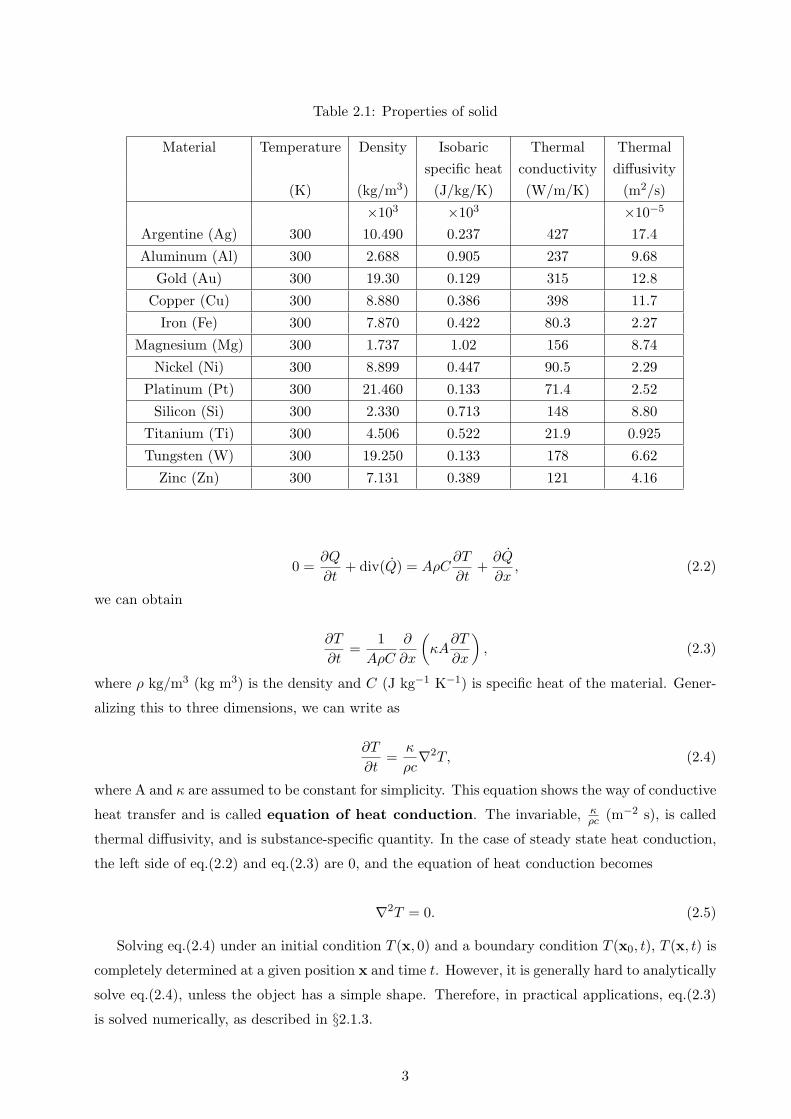
Table 2.1: Properties of solid
Material Temperature Density Isobaric Thermal Thermalspecific heat conductivity diffusivity
(K) (kg/m3) (J/kg/K) (W/m/K) (m2/s)
×103 ×103 ×10−5
Argentine (Ag) 300 10.490 0.237 427 17.4
Aluminum (Al) 300 2.688 0.905 237 9.68
Gold (Au) 300 19.30 0.129 315 12.8
Copper (Cu) 300 8.880 0.386 398 11.7
Iron (Fe) 300 7.870 0.422 80.3 2.27
Magnesium (Mg) 300 1.737 1.02 156 8.74
Nickel (Ni) 300 8.899 0.447 90.5 2.29
Platinum (Pt) 300 21.460 0.133 71.4 2.52
Silicon (Si) 300 2.330 0.713 148 8.80
Titanium (Ti) 300 4.506 0.522 21.9 0.925
Tungsten (W) 300 19.250 0.133 178 6.62
Zinc (Zn) 300 7.131 0.389 121 4.16
0 =∂Q
∂t+ div(Q) = AρC
∂T
∂t+
∂Q
∂x, (2.2)
we can obtain
∂T
∂t=
1AρC
∂
∂x
(κA
∂T
∂x
), (2.3)
where ρ kg/m3 (kg m3) is the density and C (J kg−1 K−1) is specific heat of the material. Gener-
alizing this to three dimensions, we can write as
∂T
∂t=
κ
ρc∇2T, (2.4)
where A and κ are assumed to be constant for simplicity. This equation shows the way of conductive
heat transfer and is called equation of heat conduction. The invariable, κρc (m−2 s), is called
thermal diffusivity, and is substance-specific quantity. In the case of steady state heat conduction,
the left side of eq.(2.2) and eq.(2.3) are 0, and the equation of heat conduction becomes
∇2T = 0. (2.5)
Solving eq.(2.4) under an initial condition T (x, 0) and a boundary condition T (x0, t), T (x, t) is
completely determined at a given position x and time t. However, it is generally hard to analytically
solve eq.(2.4), unless the object has a simple shape. Therefore, in practical applications, eq.(2.3)
is solved numerically, as described in §2.1.3.
3

In an object, the flow of heat between a position x1 at a temperature T1 and another position
x2 at a temperature T2 is expressed, from eq.(2.1), as
Q = K21(T2 − T1), (2.6)
where K21 (W/K) is called thermal conductance. Thus, Q is proportional to the temperature
difference ∆T between the two points. If we relate Q with electric current, ∆T with potential
difference, and K−121 with electric resistance, eq.(2.6) can be considered as analogous to the Ohm’s
law.
2.1.2 Radiative heat transfer
Every object consists of molecules and atoms, which are moving harder as the temperature gets
higher. Because of this motion, the object emits electromagnetic waves. The radiative energy
emitted per unit time and unit area from a surface of an object is called emissive power, and is
denoted here as E (W/m2). Thermal radiation from any object is emitted in various wavelengths,
and when the energy included in an wavelength interval λ ∼ λ + ∆λ is Eλdλ, E can be written as
E =∫ ∞
0Eλdλ. (2.7)
Here, Eλ is called spectral emissive power. When the object is a complete black body, the spectral
emissive power Ebλ follows a Planck distribution, and the emissive power Eb can be written as
Eb = σT 4, (2.8)
from Stephan-Boltzmann law. In this equation, σ = 5.67 × 10⁻⁸ (W/m2/K4) is the Stephan-
Boltzmann constant, and T is again the temperature of the object.
Thermal radiation of a general object is different from the black body radiation both in shape
and intensity. However, taking a black body radiation of the same temperature as a reference, E
and Eλ can be expressed in the ratio from as
E = εEb = εσT 4, (2.9)
Eλ = ελEbλ, (2.10)
where ε (0 < ε ≤ 1) is called emissivity, and ελ is monochromatic emissivity. Obviously, a black
body has ε = 1 and ελ = 1 at any λ.
Radiation energies incident upon a surface of an object are either absorbed, reflected, or going
through. The fraction of the absorbed energy is called absorptivity, and denoted as α. Like the case
of emissivity, we can also define monochromatic absorptivity, αλ. A black body is characterized as
α = αλ = 1, (2.11)
4

and general objects have 0 < α < 1 and αλ < 1.
Because thermal radiation of an object results from thermal motion of molecules constructing
the object, an object which strongly absorbs radiation at a particular wavelength also emits strongly
at the same wavelength. Therefore, we have
αν = εν , (2.12)
which is called Kilchihoff’s law.
Some caution is needed about absorption. The emissivity ε, the monochromatic emissivity ελ,
and the monochromatic absorptivity αλ are intrinsic properties of an object, but the absorptivity
α depends on the property of the incident radiation. Namely, when energy incident upon a surface
of an object in λ ∼ λ + δλ is Hλdλ, all energy is written as H =∫∞0 Hλdλ, so α is expressed as
α(T ) =∫∞0 αλHλdλ∫∞
0 Hλdλ. (2.13)
In particular, in the case of incident energy from a black body, Hλ(T ) = ε(Tb)Ebλ(Tb), and when
the temperature of the object is the same as that of a black body, Tb,
α(T ) = ε(T ) (T = Tb), (2.14)
from eq.(2.12).
2.1.3 Finite difference method
In numerically calculating a temperature distribution, we divide the object into n finite elements
and define flow of heat between every part of nodal points i and j, Qij .
Let the temperature T (x) be a continuous function of the position x. Using discrete values of
T , Ti−1, Ti, andTi+1 at discrete values of x, xi−1, and xi, xi+1, respectively, we approximate the
differential coefficient of T (x) at xi by differences as
∂T
∂x|xi =
Ti+1 − Ti
∆x+ O(∆x), (2.15)
∂T
∂x|xi =
Ti − Ti−1
∆x+ O(∆x), (2.16)
∂T
∂x|xi =
Ti+1 − Ti−1
2∆x+ O(∆x2), (2.17)
as shown in figure 2.1. These ways of expression are called finite difference; in particular, eq.(2.12) is
called forward difference expression, eq.(2.13) is called backward difference expression, and eq.(2.14)
is called central difference expression. O(∆x) and O(∆x2) shows truncation errors in the order of
∆x and ∆x2. Thus, the central difference is more accurate than the others.
In a similar way, the second-order difference coefficient is expressed as
5

Figure 2.1: Difference expression of the derivative of a continuum function (JSME text series Heattransfer figure 2.37).
∂2T
∂x2|xi =
Ti+1 − 2Ti + Ti−1
2∆x2+ O(∆x2). (2.18)
Adopting a two-dimensional case for simplicity, let us solve the thermal conduction equation,
eq.(2.3), through the difference method. If heat is not generated, and physicality values are constant
at any point in an object, eq.(2.3) is expressed as
∂T
∂t= α
(∂2T
∂x2+
∂2T
∂y2
), (2.19)
where α stands for κ/ρc. When the (x,y) plane is divided in directions x and y, step sizes of ∆x,
∆y, respectively, we can divide the object into internal elements and boundary elements. As shown
in figure 2.2, let us consider an internal element which is i-th in x-direction, and j-th in y-direction.
Denoting the temperature at t = n∆t as Tni,j , eq.(2.15) is expressed, from eq.(2.13) and eq.(2.16),
as
Tn+1i,j − Tn
i,j
∆t= α
(Tn
i−1,j − 2Tni,j + Tn
i+1,j
2∆x2+
Tni,j−1 − 2Tn
i,j + Tni,j+1
2∆y2
), (2.20)
where ∆t is a time step. In this equation, the temporal differentiation is expressed as forward
difference expression, and the space differentiation is expressed as sentral difference expression.
This includes a truncation error of O(∆x2,∆y2). When we set
6

Figure 2.2: A difference approximation of inner elements in an object (JSME text series Heattransfer figure 2.39).
rx = α∆t/∆x2, ry = α∆t/∆y2 (2.21)
the equation (2.17) becomes
Tn+1i,j = Tn
i,j + rx(Tni+1,j − 2Tn
i,j + Tni−1,j) + ry(Tn
i,j+1 − 2Tni,j + Tn
i,j−1). (2.22)
Eq. (2.21) is used in two representative context. One is initial value problems, wherein we
specify T 0i,j, and calculate evolutions of these temperatures by a step of ∆t. The other is boundary
condition problems, in which we fix the temperatures of certain nodes to specified volumes, and
repeat the iteration of eq.(2.21) until |Tn+1i,j − Tn
i,j | becomes sufficiently small. This corresponds to
a steady state condition (∂T/∂t = 0) in eq.(2.4), in either case, the heat flow Qij is easily obtained
from the solution Tni,j through eq.(2.6).
2.1.4 General heat transport equation
Generally, a variation of the temperature of an node i is written as
Ci∆Ti
∆t=∑j 6=i
Qji =∑j 6=i
Qji, (2.23)
where Ci is specific heat of node i. Here, by using eq. (2.6) and eq. (2.8), a heat transported from
node j to i in eq. (2.23) can be expressed as
QCji = KC
ji(Tj − Ti) (2.24)
Eji = KR(T 4j − T 4
i ). (2.25)
7

Eq.(2.23) can be utilized not only node connection in an individual object, but also that between
different materials.
Figure 2.3: A temperature drop by a contact resistance.(JSME text series Heat transfer figure2.13.)
as shown in figure 2.3, surfaces of different materials 1, 2 cannot be completely in contact to
each other. This is because they have concavities and convexities, so they are not parallel on
small scales. When the surfaces contact only partially, a significant resistance Rc is generated
there, which is called thermal contact resistance. Using temperatures of the two objects at the
contact points, T2A and T2B (figure 2.3), Rc is expressed as
Q =T2A − T2B
Rc. (2.26)
Because the heat flow Q in x-direction is the same at any point,
Q = κ1AT1 − T2A
L1=
T2A − T2B
Rc= κ2A
T2B − T3
L2, (2.27)
where κ1, κ2 are conductivities, while L1, L2 are lengths of the two objects (figure 2.3).
8
2.2 Thermal Control Actuators
Elements which control temperatures purposely (e.g., heating or cooling) is called thermal control
actuators. Elements which utilize active devices such as heaters and heat pipe are called active
control actuator, while those which do not utilize active devices are called passive control actuator.
The thermal control actuators related with the SGD are described in §3 in detail. Here, review
general concept of thermal control actuators.
2.2.1 Passive control actuator
Passive thermal control is realized by radiation control and conductivity control. The former
consists of absorptivity/emissivity (αs/ε) control, carried out by selecting surface properties of
materials so as to minimize or maximize the radiative heat transport, depending on the purpose.
As a typical example of the α/ε control, let us describe the technique of radiative cooling.
which is used to cool space-borne instruments including the SGD itself, as well as CCD cameras on
ASCA and Suzaku. For this purpose, we need to let let heat efficiently escape from the instrument
to the external space, and to reduce heat input from external space as much as possible. This
is Turn requires the thermal emissivity ε in infrared region should be high, and the absorptivity
αs to solar radiation and terrestrial albedo should be small, so sun face materials which have
αs/ε ∼ 0 is better. We obtain αs/ε ∼ 0.3/0.8 when we paint the surface white. However, a much
better performance is realized when aluminum which has a small αs is placed on the internal side
(satellite side), and a cover which has a high ε and optical transparency (e.g., a thin plastic film)
is placed on the external side (space side). Aluminized plastic films are typical materials with this
property. Alternatively, thin teflon films, backed up silver-evaporated layer, are utilized. In order
to intercept far-infrared radiation from other parts of the spacecraft which is usually kept at near
room temperatures, thermal blanket is utilized. A typical thermal blanket is Multilayer Insulation
(MLI), in which aluminum is interleaved by polyester-evaporated sheet and polyester net (to avoid
contacts between sheets).
Typical techniques used for conductivity control, include heat sink which moderates rapid tem-
perature variations, thermal thin filer which increases conductance at a contact point, thermal
insulation spacers which decrease thermal conductance are, and high-conductivity elements (alu-
minum, copper, graphite etc.) used to increase conductive heat flows.
2.2.2 Active control actuator
Controlling the temperature by only passive control actuators is often limited for those instruments
which generates a significant amount of heat, or those which have time-variable heat generation
(e.g., when it is put on and off), or those which is temperature critical, or those which experience
largely different thermal environments (e.g., planetary missions). Then, we utilize active control
actuators and control the temperature positively.
9

A typical active control actuator is thermal louver in which we can change αs/ε by opening or
closing shutter blade (either manually by commands, or automatically using bimetal switches/torgures).
When we would like to keep the temperature, we close the shutter and expose the surfaces with
high αs/ε, and when we would like to radiate heat out, we open it and make surface with low αs/ε
visible.
For active conductive control, heat pipes and fluid controls are often utilized. In particular,
heat pipes are good thermal conductor by utilizing latent heat of phase variation and capillary
action. Heat pipes have been utilized in the Suzaku HXD.
2.3 Thermal Environment of the Satellite
A satellite on its orbit receives heat inputs from the Sun and the Earth (albedo and far-infrared
emission), and at the same time, it radiates heat as determined by its temperature to space with
a temperature of 2.7 K . The temperature of the satellite is naturally determined by the balance
between these thermal input and output in its thermal environment.
2.3.1 Solar radiation
The Sun has a radius R = 6.96 × 10⁵ km. located D = 1.5 × 10⁸ km (≡ 1 AU) distant from
the Earth, and its radiation can be approximated by a black body with an effective temperature
T = 5780 K. Therefore, the solar radiation flux near the Earth is
S = 4πR2σT 4
/4πD2 = σT 4 = (1353 ± 21) × (1+0.034
−0.0325) ∼ 1353+46−44 W/m2, (2.28)
where the ±21 W of the right hand side reflects a range of the observation data. The second factor
represents the effect of the season variation, and it becomes maximum at the perihelion point (3rd
January), and minimum at the aphelion point (4th July).
2.3.2 Earth albedo
Of all the solar heat input to the Earth, some fraction goes back to space by atmospheric scattering
and reflection by clouds or the Earth’s surface (including sea). This is called Earth albedo. An
energy density of the albedo Sa is expressed as
Sa = aS, (2.29)
where a is an albedo coefficient. This albedo coefficient is affected strongly by conditions of the
scattering object, so it varies between 0.1 and 0.8, depends on the season, the position, and the
existence of clouds. Usually, its average is estimated as
a = 0.30+0.30−0.15. (2.30)
The wavelength distribution of the albedo is the same as that of the Sun.
10

2.3.3 Earth infrared radiation
The Earth has an equatorial radius RE = 6378 km. The temperature of the Earth is determined by
a heat budget between the thermal input from the Sun and and thermal output of itself, described
as
S(1 − a) × πR2E = εσT 4
E × 4πR2E , (2.31)
where ε refers to the infrared emissivity of the Earth. Approximating that the Earth is a block
body (ε = 1), this equation yields
TE = 254 K, (2.32)
and the radiation from the Earth is in an infrared wavelength region. In addition, the flux of the
infrared radiation can be expressed as
ϕE = εσT 4E = 237+28
−97 W/m2. (2.33)
However, considering the greenhouse effect, the temperature of the geosphere is high than (2.21).
11

Chapter 3
ASTRO-H AND THE SOFT
GAMMA-RAY DETECTOR (SGD)
3.1 ASTRO-H
The X-ray astronomy satellite, ASTRO-H, which is the successor to Suzaku, is scheduled for launch
in the fiscal year 2013. It carries onboard two types of telescopes; the Hard X-ray Telescope (HXT)
and the Soft X-ray Telescope (SXT), and four kinds of detectors; the Soft X-ray Imager (SXI), the
Soft X-ray Spectrometer (SXS), the Hard X-ray Imager (HXI), and the Soft Gamma-ray Detector
(SGD). The spacecraft will experience a typical near-Earth thermal environment (§2), because it
will be put into a near-circular orbit with a perigee of ∼ 550 km.
3.1.1 Observational capability of ASTRO-H
Outstanding capabilities of ASTRO-H include ;
• The first imaging spectroscopic observations in energies above ∼ 12 keV up to ∼ 80 keV, to
be realized by the HXT and the HXI.
• The first ultra high-resolution spectroscopic observation by the SXS, with an energy resolution
of 4.7 eV at 6 keV. This was ∼ 120 eV previously.
• An extremely broad energy band realized by a collaboration of these instruments. The softest
end (0.3 − 12 keV) is covered by the SXT + SXI and the SXS, the intermediate range
(5− 80 keV) by the HXT + HXI, and the hardest end (50− 600 keV) by the SGD. Although
the overall bandpass is nominally the same as that of Suzaku, the sensitivity at ≥ 10 keV is
significantly improved.
The basic parameters of all instruments onboard ASTRO-H are summarized in Table 3.1.
12

Hard X–ray Imaging System (HXT+HXI)
Focal Length 12 mEffective Area 300 cm2 (at 30 keV)Energy Range 5–80 keVAngular Resolution <1.7 arcmin (HPD)Effective FOV ∼9×9 arcmiin (12 m Focal Length)Energy Resolution <1.5 keV (FWHM, at 60 keV)Timing Resolution several 10 µsDetector Background <1–3×10⁻⁴ cts s−1 cm−2 keV−1
Operating Temperature ∼ –20C
Soft X–ray Spectrometer System (SXT–S+XCS)
Focal Length 5.6 mEffective Area 210 cm2 (at 6 keV)
160 cm2 (at 1 keV)Energy Range 0.3–12 keVAngular Resolution <1.7 arcmin (HPD)Effective FOV ∼3×3 arcmiinEnergy Resolution 7 eV (FWHM, at 6 keV)Timing Resolution 80 µsDetector Background <6×10⁻³ cts s−1 cm−2 keV−1
Operating Temperature 50 mK
Soft X–ray Imaging System (SXT–I+SXI)
Focal Length 5.6 mEffective Area 360 cm2 (at 6 keV)Energy Range 0.4–12 keVAngular Resolution <1.7 arcmin (HPD)Effective FOV ∼38×38 arcmiinEnergy Resolution <150 eV (FWHM, at 6 keV)Timing Resolution 4 secDetector Background <a few×10−3 cts s−1 cm−2 keV−1
Operating Temperature –120C
Soft Gamma–ray non–Imaging System (SGD)
Energy Range a few 10 keV–600 keVEnergy Resolution ∼2 keV (FWHM, at 40 keV)Geometrical Area 210 cm2
Effective Area ∼30 cm2 (Compton mode, at 100 keV)FOV 0.6×0.6 deg2 (<150 keV)Timing Resolution several 10 µsDetector Background <a few×10−6 cts s−1 cm−2 keV−1
(100–200 keV)Operating Temperature ∼ –20C
Table 3.1: Specification of instruments.
13

3.1.2 Expected achievements of ASTRO-H
As an example of a large number of research highlights to be expected with ASTRO-H, we select
one particular subject, Active Galactic Nuclei (AGN). Figure 3.1 shows the simulated broad band
spectra of the typical bright Type I Seyfert galaxy, Mrk 509, actually abserved with Suzaku and
simulated for ASTRO-H. The energy range is both 0.3 − 600 keV. We can see that the sensitivity
of ASTRO-H is much better than that of Suzaku, particularly in the hard X-ray band which are
covered by the HXI and the SGD. Because the HXD has a sensitivity of a few mCrab at around
50 − 200 keV, the expected high energy cutoff of AGNs may not be easily observed. However, by
using the SGD and the HXI, it is clearly observed as shown in figure 3.1. The wide energy band
with high sensitivity will reveal spectral components in the hard X-ray spectra of many types of
AGNs and identify their nature (e.g., Noda et al. 2011[7]).
In the soft X-ray band, the SXS can be utilized to resolve narrow Fe-K line or Fe-K edge. Using
these parameters, the intensity of secondary components scattered far from the central BH will be
accurately determined. Furthermore, ionized absorbers which are reported to exist in many AGNs
can be individually resolved, These observations will provide a key to clarifying will whether the
relativistically broadened Fe-K lines reported in Seyferts such as MCG–6-30-15 are real or not.
(a) (b)
Figure 3.1: Broad band spectra of the typical Type I Seyfert Mrk 509. Panel (a) shows actualSuzaku spectra, while (b) the simulated ASTRO-H spectra.
3.2 The Soft Gamma-ray Detector (SGD)
The Soft Gamma-ray Detector (SGD) covers an energy range of 60–600 keV, which is the highest
part among the detectors onboard ASTRO-H. The SGD consists of two units of detectors called
SGD-S, and an electronics called SGD-E. As shown in figure 3.2, each SGD-S consists of three
Compton Cameras, active BGO shields, front-end electronics, thermal harness, and structure. The
14

(a) (b)
Figure 3.2: One unit of SGD-S, comprising three Compton Camera, displayed by 3D CAD. (left)An overall view, including the radiator panel (purple). (right) An expanded view of the threeCompton Cameras, surrounded by active shields (green).
two SGD-S units are attached to outer face of the spacecraft side panels, so that they are exposed to
direct Sunshine, or to the 2.7 K space. Therefore, it requires very careful thermal design, although
the present thesis focus on thermal design of a single Compton Camera rather than the entire
SGD-S. The SGD is being developed by the Stanford University, Nagoya University, JAXA, The
University of Tokyo, Hiroshima University, and Saitama University.
3.2.1 Compton Camera
(a) (b) (c)
Figure 3.3: The concepts of the Compton reconstruction in the Compton Camera. (a) Comptonkinematics. (b) Algorithm of source detection. (c) A Compton Camera with a collimated field ofview.
The Compton Camera (identical 3×2 units in total) is the detection part of SGD-S, and works
as one of the world’s first detectors that utilize Compton kinematics. Each camera consists of 32
15

Si layers, 8 CdTe layers, and 8 side CdTe layers. All of them are solid-state detectors with fine
position resolutions, and are accommodated tightly in a small volume of 124 mm×124 mm×120 mm.
Basically, Compton-scatters an incident gamma-ray photon at one of the Si layers, and photo-
absorbs the scattered photon at CdTe layers. Let the position and energy recorded at the scattering
site ~r1 and E1, respectively, and those at the absorbing site ~r2 and E2. The scattering angle θ
between the incident direction and ~r1 − ~r2 is expressed as
cos θ = 1 +mec
2
E1 + E2− mec
2
E2(3.1)
from Compton kinematics. Solving this equation inversely for θ utilizing the two energy measure-
ments (E1,E2), and further using the two interaction points (~r1,~r2), the incident direction of the
photon is constrained to be a circle as shown in figure 3.3a. The source direction can be determined
as a point at which a large number of circles overlap, as shown in figure 3.3b. In addition to this
Compton kinematics, the field of view of each Compton Camera is both actively and passively
collimated to 9.7 × 9.7 and 34’ × 34’, respectively (figure 3.3b; also see below). By requiring
each valid event to arrive through this small aperture, we can make each Compton circle an arc,
and hence narrow down the source location. Using this Compton re-construction, we can also
reject events which have inconsistent arrival directions, such as events due to decays of radio-active
materials created in orbit, and neutron scattering signals, because they are basically isotropic. As a
result, we can decrease back ground in the Compton Camera. Even though its detection efficiency
is relatively low, 15% at ∼100 keV, a combined use of 3 × 2 cameras will provide an order of
magnitude higher sensitivity than with the Suzaku HXD.
3.2.2 Active shields and fine collimators
Any satellite-borne radiation detector needs some kind of radiation shield, because the radiation
background in space is considerably higher than that on ground. However, conventional passive
shields, such as lead blocks, are too heavy to utilize. Therefore, we use active shields of BGO
(Bi4Ge3O12) crystal scintillators. Thanks to time information of optical photons emitted by BGO,
we can remove events in the Compton Camera that have simultaneous hits in BGO. By this anti-
coincidence technique, we can remove such background components as; charged particles penetrat-
ing SGD-S; secondary photons produced by cosmic-ray interactions with the detector materials;
and background γ-rays that scatter in the shield and enter the Compton Camera. The active
shield also works to remove those signal photons which are scattered in the Compton Camera,
and escaped out. In addition, BGO can stop protons which have energies of less than 100 MeV,
and reduce activation of detector materials by such protons. Similarly, BGO absorbs photons (up
to ∼ 300 keV) that comes from outside the narrow shield opening (including cosmic background
photons and other celestial sources). That is, BGO can also behave as passive shields.
Like in the Suzaku HXD, the SGD active shields have a tightly collimated configuration, leaving
only a narrow opening (field of view) used to observe target object. However, it is difficult to make
16

this filed of view narrower by using BGO crystals. It is made of phosphor bronze, and has a
thickness of 100 µm, so it can stop photons of up to 150 keV energies. The field of view (FOV) is
34’ ×34’. After re-construction by the Compton kinematics in the Compton Camera, if directions
of incident photons are out of the FOV, we can judge that they are background events, particularly
decay of activated isotopes (figure 3.3c), and remove.
3.2.3 Thermal environments and requirements of the SGD
In the SGD, mainly, two components are temperature critical, One is the Compton Cameras
(§3.2.2), in which the temperatures of all semi-conductor layers must be below −15C. This is
the main theme of the present thesis, and the detailed thermal design is explained on in Chapter
4–6. The other is the active shield (§3.2.2), which must also be used preferably in temperature
below −15C. This has merits; one is that the APD leak current gets lower, at lower temperatures,
and hence the APD noise is reduced. Another is that we need a less bias voltage to obtain a
required APD gain. Finally, the BGO light output increases toward lower temperatures. In short,
both the Compton Cameras and the active shields need a low temperature at −15C to −20C.
Inside one SGD-S, the three Compton Cameras generate total 17.6 W heat, the four charge
sensitive amplifiers (APD-CSAs, figure 3.2 blue parts) total 5.2 W, the High Voltage box (HV)
1.0 W, and the Point of Load (POL) 3.0 W. Therefore, a total 25.8 W heat is generated inside. In
addition, because the SGD is fixed outside the satellite body (§3.2), the Solar radiation and the
Earth Albedo, the Earth far-infrared radiation (§2.6) are directly incoming. Furthermore, in the
worst case, the temperature of the Solar Array Paddles (SAP) reaches 100C, and it radiates heat
to the SGD as a black body (§2.2).
(a) (b)
Figure 3.4: Appearances of (a) radiator and heat pipes and (b) cold plate (light green).
To keep the temperature of the SGD low enough under such a tough environment, thermal
harnesses such including a radiator and two heat pipes are utilized (§2.5). They are illustrated
in figure 3.4a. The heat pipes transport the heat from SGD-S to the radiator panel, where it is
17
radiated (§2.2.2) to space. As shown in figure 3.4b, we use a “cold plate”, made of aluminum from
the Compton Cameras to lead the heat to the bottom plate.
18

Chapter 4
THERMAL REQUIREMENTS AND
RESEARCH PLAN
4.1 Thermal requirement for the Compton Camera
Performance of semi-conductor devices such as Si and CdTe depends on its temperature strongly.
Generally, thermal noise increases as the temperature gets higher. In the case of CdTe, in addition,
the detector gain decreases on a considerably shorter time scales at higher temperatures, due to
an enhanced trapping of carries in impurity level (Polarization). In any case, the energy resolution
of semi-conductor devices gets worse, as the temperature increases, so their temperatures must be
kept low enough. To realize the resolution of the Compton Camera of 2 keV (FWHM) at 40 keV,
its temperature must be below −15C from top to bottom.
The SGD team defines the temperature of the cold plate to be -20C, so we must design the
Compton Camera so that all its components must be kept in a temperature between −20C and
−15C.
4.2 Thermal problems in the Compton Camera
As illustrated in figure 4.1, each Compton Camera consists mainly of 20 swastika-shaped “trays”,
each carrying on its both sides pixellated (16 × 16) semiconductor devices; the top 16 trays have
Si-detectors, whereas the bottom 4 CdTe-devices. In each tray, the 512 (16 × 16 × two sides)
output signals are read by 4 ASICs, which are placed at the four corners of the tray. Their power
consumption is 0.021 W per ASIC, 0.16 W per tray, 0.82 W per corner, and 3.2 W in total. In
addition, ASICs for side CdTe detectors generate heat of 0.252 W per one corner, so total 1.01 W
in every surface. Then, to make the temperature gradient within the Compton Camera less than
5C (§4.1), we need to transport efficiently the heat at each corner vertically down to the cold plate
at the bottom.
Figure 4.1 shows how the 20 trays are stacked; thus, each tray (pink) touches the upper and
lower neighbors. Employing the simplest thermal design which utilizes only these contacts for a
19

Figure 4.1: The geometry of trays (pink), a bottom frame (purple), and a cold plate (green) in theCompton Camera. This is shown by 3DCAD.
heat path, let us quickly estimate by hand temperature distribution in the Compton Camera by.
Here, the contact area between the adjacent trays is assumed as 100 mm2 and the thickness of
tray is 7 mm. Even if the trays on which the semi-conductors and ASICs are placed are made of
aluminum, and ignoring contact resistances between the trays, the temperature of the top layer
tray was found to become −10C (That is, ∆T = 10C). However, aluminum cannot be utilized as
a tray material, and because aluminum photo-absorbs ∼10% of photons after Compton-scattering
at Si layers. Therefore, we must choose a nonconductor and low-Z material like a plastic which
are sufficiently transparent to the scattered signal photons. If we instead use, for example Poly
Benz Imidazol (PBI), which is one of plastic materials, the vertical temperature gradient would
amount to > 200C, in inverse proportion to the thermal conductivity between Al and PBI. Thus,
the thermal design of the Compton Camera encounters a serious problem.
4.3 Suggested Solutions
To solve the problem shown in §4.2, we need new efficient heat paths which enable heat of the ASICs
to flow toward the aluminum cold plate with a much smaller temperature difference. Such the heat
20

paths can be divided into vertical ones, which go through all trays and reach the aluminum cold
plate, and parallel ones, which run from individual ASICs to the vertical ones. The vertical paths
should be high-conductive poles because all heat of the trays (0.82 W each) gathers into them,
while the parallel ones should be thin enough to be laid under Front End Card (FEC). Therefore,
we have decided to use as our baseline design, metals for the vertical ones, and thin heat-conductive
sheets for the parallel ones.
For the vertical path, which metal is the most appropriate? Although silver is the most heat-
conductive material (conductivity κ = 427 W/m/K), it is much less suited machining than copper
which is the second heat-conductive one (κ = 398 W/m/K). Therefore, we employ copper as
the material of the vertical heat paths. For the parallel paths, thin sheets which have a high
heat conductance along their plane are appropriate. One candidate is power supply paths for the
ASICs, which are 100 µm thin copper layers set between glass epoxy boards in FEC. However, they
are connected by some thin through holes, so the temperature difference between an ASIC and a
copper pole becomes ∼ 3C if we rely only on this path. Therefore, have decided to significantly
strengthen this path by adding a 100 µm thick graphite sheet which have a high conductivity of
700 W/m/K along its plane.
As shown in figure 4.2, the Compton Camera has box-shaped side wells, made of aluminum plate
of 2 mm thickness. Because this shield can be considered as an additional vertical heat path, an
attractive design is thermally couple these side plates to the proposed copper poles, in an attempts
to increase the overall vertical thermal conductivity. The aluminum bottom frame (figure 4.2) can
be utilized as yet bottom heat path, which is particularly suited in extracting heat out of the side
CdTe detectors.
4.4 Research Plan
The principal objective of the present thesis is to solve the serious thermal issue of the SGD
Compton Camera (§4.2), by pursuing the suggested solutions described above (§4.3). Specifically,
we attempt to fix the baseline thermal design of the Compton Camera, which will be utilized to
fabricate an engineering model (EM) of SGD-S. The EM design, with a minimum modification,
will be then fed to the production of the flight model (FM) to be actually put in orbit.
Following the general procedure of thermal design of satellite-borne instruments, in §5 we first
construct a thermal mathematical model. Such a calculation is particularly effective in cases like
this, because we can ignore convective heat transfer, which is the most difficult to model numerically.
Thus, we construct a thermal mathematical model, and search the most appropriate thermal design
which fills the thermal requirements by changing parameters in that model. However, it has a
significant shortcoming, that contact conductances (contact resistances) at each contact point must
be assumed.
To measure the actual contact conductances, and to verify the overall validity of the design, we
21

Figure 4.2: The same as figure 4.2, but the aluminum side plates (green), the copper pole for heatconduction (purple), and the graphite sheets (blue) are added. This becomes our baseline thermaldesign.
perform in §6 a verification experiment. This utilizes thermal dummies which have the same main
heat paths as the thermal mathematical model.
These dummies have the same size as the actual Compton Camera, and fed with the same heat
input as from the ASICs. By measuring temperature distributions of the thermal dummy, we can
calibrate the thermal mathematical model, and estimate in particular the contact conductances.
Finally, we can use the calibrated thermal mathematical model to finalize our thermal design
of the Compton Camera. Furthermore, if any change in design of the Compton Camera because
of some of the electrical or mechanical requirements, we can easily predict the expected impact on
the thermal condition.
22

Chapter 5
THERMAL MATHEMATICAL
MODEL OF THE COMPTON
CAMARA
In this Chapter, a thermal mathematical model (TMM) of the Compton Camera is constructed,
and is used to calculate temperature distributions therein. First, we explain the software used
in simulation, Thermal Desktop (TD), and next, assume contact conductances at several contact
points. Then, we calculate temperature distributions of the Compton Camera in different cases
step by step, and fix its baseline thermal design which fulfills the thermal requirements.
5.1 Thermal Desktop(TD)
Thermal Desktop (TD) is a software to construct a numerical model of a thermal design, and to
calculate steady-state temperature distributions and heat flows, as well as their time variations in
dynamical (time-varying) applications. We can build up a geometry of an instrument in autoCAD,
and divide each part into some nodes as many as we would like to. Then, we can assign any heat
input at each node, and specify conductive and radiative couplings between any pair of nodes.
After constructing the geometry, a temperature distribution can be calculated by an analysis code
called SINDA/FLUINT, which utilizes finite difference method (§2.1.2). The result of calculation
can be displayed by color contours which specify the temperature.
5.2 Mathematical Model Construction
5.2.1 Model components
As shown in §4.2, the graphite sheets provide the main parallel heat paths in the Compton Cam-
era, and the copper poles are main vertical ones. In addition, the aluminum side shield and the
aluminum bottom frame are considered to provide additional heat paths. Therefore, we construct
models of these components as shown in figure 5.1 left. The figure also shows a semi-conductor
23

Figure 5.1: Left figure shows thermal parts of the one-side Compton Camera. A semi-conductor(blue), a ASIC (red), a graphite sheet (black), a copper pole (orange), a bottom frame(purple), and an aluminum electro-magnetic shield (grey) are placed at their position in the actualCompton Camera. Right shows a crude shape of the graphite sheet, in which a dashed line showsa fold line, and it is utilized by being folded at this line.
device as well as the input heat generated by ASICs. A piece of graphite sheet is folded at the
center as shown in figure 5.1 right, and put on the both surfaces of the tray. Our major task is how
we thermally connected these components together
The Compton Camera has a 90 rotational symmetry, and all the four sides are considered to
have same the temperature distributions; so we display only one side of the Compton Camera.
Furthermore, Although we model all the 40 trays in the same manner, for simplicity, we hereafter
display only the top layer, which has the highest temperature of all 40 layers.
5.2.2 Node division
Each component shown in figure 5.1 is divided into a certain number of nodes. The number of the
nodes in each component is decided, depending on how finely we would like to know a temperature
distribution therein. However, when the number increases, the calculation time also increases.
Therefore, the node division should be optimized by a balance between the model resolution and
the calculation time.
Figure 5.2 shows our node division of each component in the one-side Compton Camera. Each
24

semi-conductor device
Graphite sheet
Copper poleBottom frame
Shield plate
Figure 5.2: Our node division of each component in the one-side Compton Camera.
semi-conductor device is divided into 5 × 5 nodes, a graphite sheet into (2 × 3 + 3 × 5) × 2 nodes,
the copper pole into 4 × 50, the bottom frame actually its quarter into 8 × 8 + 8 × 5, and the side
shield panel into 13 × 50.
5.2.3 Node couplings
In a TMM, the divided nodes must be properly connected to one another. There are three forms
of node couplings; conductive coupling, radiative coupling, and contact coupling. Here, we limit
“conductive coupling” to mean heat conduction within the same material, and use the term “contact
coupling” to mean that between two materials across a certain interface (e.g., a simple contact,
glue, adhesive tapes, etc). This is because contact thermal resistance can be major obstacles of
heat transport under the absence of convection.
The conductive coupling between a pair of nodes is calculated as,
K =A
d× κ, (5.1)
where A is contact area, d is separation between them, and κ is conductivity of a material of the
component.
The wattage transferred by radiation form one node with a temperature T + ∆T to another
with a temperature T , is calculated as,
E = ε1ε2σA((T + ∆T )4 − T 4) × Ω/2π (5.2)
∼ 4εασAT 3∆T × Ω/2π, (5.3)
25

where A is area on a surface of radiating node, Ω is a solid angle viewing the surface, ε1, ε2 are
emissivities of the radiating node and receiving nodes. ∆T T is assumed, in the transformation
of this equation.
Between a pair of nodes which are in contact with each other, a contact resistance appears, and
becomes the dominant coupling between them; so in constructing a TMM, these contact resistances
must be assumed. The way of estimating them is explained in the next subsection.
5.2.4 Assumption on screw-contact conductances
The present TMM involves two types of contact conductances. One is between a graphite sheet
and a copper pole, and the other is between metals. These two types of contact conductances are
considered to be both related to sizes of screws which fix the two surfaces together.
Table 5.1 shows empirical contact conductances, from two literatures ([3],[4]), between two
aluminum plates with clean mill rolled surface finish, bolted together with a screw using stan-
dard torque for spacecrafts. It is assumed that heat flows from one plate to the other through a
compressed area around the screw, rather than through the screw itself.
The values in Table 5.1 are visualized in figure 5.3. Thus, the contact conductance increases
with the screw diameter, because a larger area is pressed together with larger force. We can also
see that thicker plates give higher conductances. However, the two literatures are inconsistent
with each other, one reporting rather linear dependences on the screw diameter, whereas the other
parabolic relations.
In constructing our TMM, we adopt a parabolic dependence as,
K = 0.05 × (0.4 × D)2 (W/K), (5.4)
where D is the diameter of screw in mm. This relation is utilized in thermal designs in industries,
and corresponds nearly to the worst case in figure 5.3. Table 5.2 shows the contact conductance
values as a function of D, calculated by eq.(5.4). We start constructing our TMM using tentatively
these values at every contact point, even though it is not clear if they are applicable to graphite
sheets.
5.2.5 An equivalent thermal circuit
Figure 5.4 shows a thermal equivalent circuit of the one-side Compton Camera. For simplicity, we
ignore low-conductive connections that are parallel to highly-conductive ones.
Let us show a few examples of conductive coupling calculations. Trays, which are made of
PBI, have 0.41 W/m/K conductivities, so the tray conductance from semi-conductor device to the
graphite sheet with A ∼7 mm×1 mm and d is ∼3 mm, is calculate from eq.(5.1) as
K =7 (mm) × 1 (mm)
3 (mm)× 0.00041 (W/mm/K) = 0.001 (W/K). (5.5)
26

Table 5.1: Contact conductances between two aluminum plates bolted together with a screw,measured for different plate thicknesses and bolt diameters (Spacecraft Thermal Control Handbook,P266, Table 8.6). TRW and LM specify reports employed.
Diam TRW Large LM Plate Thickness (mm) TRW Small(mm) Thin Surface 1.57 mm 3.18 mm 6.35 mm 9.53 mm Stiff Surfaces
2.8 0.13 0.08 - - - 0.213.5 0.18 0.15 0.45 - - 0.264.2 0.26 0.22 0.67 1.33 - 0.424.8 0.53 0.33 1.00 2.00 3.33 0.86.4 1.05 0.48 1.43 5.26 4.35 1.327.9 - 0.67 2.00 4.00 5.88 3.579.5 - - 2.5 5.26 7.69 -11.1 - - - 6.25 9.09 -12.7 - - - - 11.11 -
Table 5.2: Values of assumed contact conductanceScrew Diameter (mm) Contact conductance (W/K)
5 0.24 0.1283 0.0722 0.032
1.4 0.01568
On the other hand, conductance of the aluminum wire bondings (φ 50 µm × 64) is calculated as,
K =0.05 (mm) × 0.05 (mm) × π × 64
3 (mm)× 0.237 (W/mm/K) = 0.04 (W/K), (5.6)
which is 40 times larger than the conductances of trays. We therefore neglect the former.
Assuming ε1 ∼ ε2 ∼ 1 and T0 ∼ −15C. we obtain the E/∆T to the next layers from eq.(5.3)
as
E/∆T ∼ 4.0 × 5.7 × 10−14 × 600 × 2583 ∼ 0.0024 W/K, (5.7)
where A ∼ 600 mm2, and Ω ∼ 2π. The temperature difference between a pair of adjacent layers is
less than 0.5C, so the radiated heat is 0.0012, which is ∼5% of the heat generated by ASIC. For
these reasons, hereafter, we ignore the conductions of trays and the radiative coupling between a
pair of adjacent layers.
27

Figure 5.3: Relations between the screw diameter and the contact conductance per screw in variouscases ([3], [4]). The aluminum plate thickness is specified by colors. The purple line representseq.(5.4).
5.3 Temperature Distribution Simulated By TD
In Chapter 4, we suggested that copper poles and graphite sheets are needed to enhance the vertical
heat paths in the Compton Camera. In order to examine whether this concept is successful, we use
the TMM family constructed in §5.2 to calculate the temperature distribution within the Compton
Camera. After a brief evaluation of lateral heat transport in §5.3.2, we begin with the case of only
a copper pole (§5.3.2), the adding an aluminum shield plate (§5.3.3), and finally incorporating a
bottom aluminum frame. The results are shown as the color contour related with temperatures.
5.3.1 Graphite sheet connection to the copper pole
Between an ASIC and the proposed graphite sheet, there is a Front End Card (FEC) which four
electrode layers separated by three glass epoxy layers. The FEC has 35 (just under ASIC) + 80
through holes, made of copper, which directly connects the top and bottom electrode planes, also
made of copper. The 35 through holes just below the ASIC individually have a diameter of 0.2 mm,
a well thickness of 0.05 mm, and a length of 0.4 mm. We can calculate total heat conductance
KT.H. as
KT.H. = 35 × 0.2 (mm) × π × 0.05 (mm)0.4 (mm)
× 0.391 (W/mm/K) = 1.1 (W/K), (5.8)
from eq. (5.1). Compared to this, conduction through the bulk of FEC (glass epoxy with K =
0.08 W/K) is negligibly small. The thermal coupling between ASIC and the top electrode plane,
28

Figure 5.4: A thermal equivalent circuit of the Compton Camera. Red blocks show ASICs whichgenerate 0.021 W individually, Cyan blocks show semi-conductor devices, (Si or CdTe), and a blueblock shows the cold plate. Abbreviations; W.B. is wire bonding, T.H. is through hole, G.S. isgraphite sheet, and C.R. is contact resistance. Black lines show conduction or contact couplings,while orange arrows radiative couplings.
and between the bottom electrode plane and the graphite sheet, are both achieved by double-faced
tapes. The tape is assumed to have a conductivity 0.0002 W/mm/K. We assume the contact
area to be 50 mm2 between the ASIC and the top electrode plane, that to be 250 mm2 between
the bottom electrode plane and the graphite sheet, and the thickness of the tape to be 100 µm.
Combing these conductances (i.e., summing up the corresponding thermal resistance), the overall
conductance between ASIC and the graphite sheet is calculated to be 0.15 W/K. Beneath FEC,
graphite sheet, which has a conductance of 0.047 W/K, is laid.
Because the copper pole cannot be thicker than 4 × 20 mm2 (due to space limitation), we
tentatively connect the graphite sheet to the copper pole by M1.4 screws, the smallest ones that
are usually available. This means a contact conductance to be 0.016 W/K, according to table 5.2.
With these assumptions, we calculated, with TD, the temperature distribution from ASIC to the
connection point to the copper pole. In this calculation, as a boundary condition, the contact
point on the copper pole is fixed to be 0C. Figure 5.5 shows the result, and the color contours
represents ∆T from the copper pole. The semi-conductor device takes the same temperature as the
29

heat input points on the graphite sheets, because the semi-conductor is connected to nowhere else.
Thus, the temperature difference between the ASIC-side and the copper-pole-side on the graphite
sheet is 1.3C, showing that the graphite sheet is very effective. However, the temperature drops
drop across the contact point with the copper pole is 2.7C, which is significant when compared to
the total temperature difference between the Si semi-conductor device and the copper pole, 4C.
The contact conductance by a M 1.4 screw, between the graphite sheet and the copper pole, is too
small.
base temperatue 0
Figure 5.5: The temperature distribution in color scale in the Si semi-conductor device and thegraphite sheet. in the case of a M1.4 screw contact between a graphite sheet and the copper polenot shown. The 0.021 W heat from an ASIC is input to the Si semi-conductor device end of eachgraphite sheet. The base temperature is fixed at 0C, and only one layer of tray is considered.Since tray has a Si device and an ASIC on its either side, the model involves two graphite sheets,although only one of the two Si devices are shown for simplicity.
To make the lateral heat paths more efficient, let us consider an alternative case wherein
we use the a double-faced tape which has a conductivity of 0.2 W/m/K, and it has an area of
3 (mm)×10 (mm)=30 (mm2), and a thickness of 0.1 mm. Then, the contact conductance there is
calculated as
K =3 (mm) × 8 (mm)
0.1 (mm)× 0.0002 (W/mm/K) = 0.05 (W/K). (5.9)
from eq.(5.1) The result of this calculation is shown in fig 5.6. Because each of ASICs generate
0.042 W, the temperature difference becomes 0.8C at the contact point, between the graphite
30

sheet and the copper pole. Thanks to this new design, the temperature difference between the top
Si semi-conductor device and the copper pole is 2C, which is nearly half as large as before. From
here, the TMM utilizes the tapes to fix the graphite sheet,
base temperatue 0
Figure 5.6: The same as figure 5.5, but the graphite sheet is attached to the copper pole using adouble-faced tape with a high thermal conductivity.
5.3.2 Case1 : only a copper pole
In §5.3.1, we focused on the lateral thermal conduction. Hereafter, the vertical one is examined.
Here the temperature distribution was calculated in the case of using only a copper pole as the
vertical main heat path. First, only a M5 screw was utilized to connect the copper pole to the
aluminum cold plate. The result of a TD simulation, performed with this condition together with
the lateral path considered in §5.3.1, is shown in figure 5.7. The result is displayed with color
contours related to temperatures. Because the figure becomes hard to see if all layers are included,
we showed only the top layer, but included all heat which all layer generate. The temperature of
the top part of the copper pole became −13.4C, while that of the bottom part −15.8C. Their
temperature difference is thus 2.4C. Because the contact conductance between the copper pole and
the aluminum cold plate was assumed to be 0.2 W/K (Table 5.2), a large temperature difference
of 4.2C is needed to conduct the total 0.84 W heat. Due to this offset, the temperature of the Si
semi-conductor device becomes −11.2C, and the thermal requirement is not fulfilled.
Then, we added another M5 screw to the contact point between the copper pole and the
aluminum cold plate; there are now two M5 screws at that point, and the contact conductance
31

Figure 5.7: The temperature distribution in the top Si semi-conductor, the graphite sheet, and thecopper pole. The graphite sheet is connected to the copper pole by a double-faced tape, and thecopper pole is connected to the aluminum cold plate by a M5 screw. A 0.021 W of heat is to eachgraphite sheet of every layer. The base temperature which is the temperature of the aluminumcold plate is fixed at −20C. Although the model incorporates 20 trays, only the top one is shownfor clarity.
there is doubled to, 0.4 W/K. The simulation result of this case is shown in figure 5.8. Thus, the
temperature gradient along the copper pole is the same as before, namely 2.2C, the temperature
drop from the copper pole to the aluminum cold plate was halved, to became 2.2C. Therefore,
the temperature of the top Si device becomes −13.4C, which is 2.2C lower than the former case.
Hereafter, we call this design “Case 1”.
Although this design does not yet meet the thermal requirement, the number of screws between
the copper pole and the aluminum cold plate cannot be increased, because of the space limitation.
Therefore, we must improve the vertical bulk heat paths, for example, by increasing thickness of
the copper pole. Due to similar space limitation, it is not feasible to make the copper pole thicker
than this, either.
5.3.3 Case 2 : a copper pole and an aluminum shield plate
To enhance the vertical heat flow, let us consider using the aluminum electro-magnetic side shield
plate as an additional heat path. As shown in figure 4.2, each of the four side shield plates has a
thickness of 2 mm, a breadth of 120 mm, a length of 120 mm, and a conductivity of 138 W/m/K.
32

Figure 5.8: The same as figure 5.7, but a M5 screw is added between the copper pole and thealuminum cold plate.
Thanks to this large cross section and the high thermal conductivity of aluminum (A5052), one
shield plate has an almost same thermal conductance as that of a copper pole. However, in their
originated design, they were not connected thermally to the trays. We hence consider connecting
the copper pole to the shield plate tightly, using thirteen M2 screws, and connect the shield plate
to the aluminum cold plate using three M3 screws. The number of these screws are maximized
considering the space available for them.
We modified the TMM including these changes, and re-calculated the temperature distribution
of the Compton Camera. The result is shown in figure 5.9. Thus, the temperature gradient along the
copper pole has decreased to 1.2C, while that between the top and bottom part of the aluminum
shield is 0.4C. Since the former is nearly halved from the previous Case 1, the copper pole and
the aluminum shield plate are estimated to have comparable contributions to the vertical heat
flow, with the M2 screws working efficiently. Thanks to this additional heat path, the temperature
difference between the copper pole and the aluminum cold plate became 1.4C, about two thirds
of Case 1. The temperature of the top Si device becomes −15.0C, which is by 1.6C lower than
Case 1. This satisfies the thermal requirement of the Compton Camera, so including the aluminum
shield as a vertical bulk heat path is considered to be very efficient. Hereafter, we call this design
“Case 2”.
33

Figure 5.9: The same as figure 5.8, but the 2 mm-thick aluminum side plate is added.
5.3.4 Case 3 : Inclusion of side CdTe detectors
Although the TMM based on the above Case 2 design meets the thermal requirements, this is not
enough for the whole thermal design of the Compton Camera. This is because on each side, side
CdTe devices are placed, and 48 ASICs which generate total 1.08 W heat (or 0.252 W per side)
are placed there to read signals. Their heat must be included into our TMM.
The heat from ASICs for the side CdTe devices can be transported directly to the bottom
frame, which is placed under lowermost tray. For this purpose, we connect the aluminum bottom
frame to the cold plate by two M5 screws. Hereafter, this version of TMM is called Case 3.
Figure 5.10 shows the TMM results for Case 3, and figure 5.11 shows more detailed temperatures
at some points of the one-side Compton Camera. The temperature distribution has been somewhat
improved from Case 2. This is because the bottom frame has a large cross-section area, and it is
tightly connected to the cold plate by a M5 screw. Therefore, it can conduct not only the heat
from the side CdTe ASICs, but some fraction of the heat from the 40 trays.
Thus, we have achieved a thermal design which fulfills the thermal requirements. This design,
namely Case 3, incorporates a graphite sheet per tray, a copper pole per side, an aluminum electro-
magnetic shield plate per side, and an aluminum bottom frame. The temperatures of all layers
can be less than −15C. However, it must be kept in mind that the results obtained here depend
strongly on the assumed contact conductances among some nodes of the TMM. We summarize
these assumptions in figure 5.11 (b), as a help to Chapter 6 where verification experiments are
34

Figure 5.10: The same as figure 5.9, but the aluminum bottom frame is added. The 0.252 W heatwhich is generated by the side CdTe ASICs is input to this frame.
carried out.
35

Figure 5.11: Temperature (green boxes) at some points calculated by our TMM for Case 3.
36
Chapter 6
VERIFICATION EXPERIMENTS
The verification experiment is divided into two parts, which utilize different thermal dummies of the
Compton Camera. One is meant for measurements of the contact conductance between a graphite
sheet and a copper pole, using a simple thermal dummy. The other is for measurements of the
vertical heat conductance, using a more faithful one.
6.1 Setup of Thermal Experiments
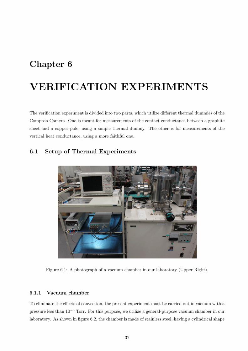
Figure 6.1: A photograph of a vacuum chamber in our laboratory (Upper Right).
6.1.1 Vacuum chamber
To eliminate the effects of convection, the present experiment must be carried out in vacuum with a
pressure less than 10−3 Torr. For this purpose, we utilize a general-purpose vacuum chamber in our
laboratory. As shown in figure 6.2, the chamber is made of stainless steel, having a cylindrical shape
37

Figure 6.2: A block diagram of the vacuum chamber.
of 240 mm (diameter) × 250 mm (height). As illustrated in figure 6.2, it is evacuated to 10−5 Torr
by a turbo-molecular pump (50 l/sec), backed up with a rotary pump (100 l/min). The chamber
pressure is measured with a Pirani gauge and an ionization vacuum gauge. The temperature of the
chamber is almost the same as that of our experiment room, ∼ 25C.
6.1.2 Heaters and thermometers
To supply heat input to a thermal dummy, 100 Ω flat-package resistors are used as heaters, because
they are easily attached to surfaces of the thermal dummy. A constant voltage of 8.9 V is applied
to each resistor to generate a heat of 0.8 W, which is the same value as the heat generated by all
the ASICs in the one-side Compton Camera. By monitoring the current, and examining whether
it is constant at 89 mA, we can confirm if the exact power is provided.
To measure temperatures at various points on the thermal dummy, Pt resistance thermometers
are used. Their resistances depend on the temperature as
RPt (Ω) = 100 + 0.38T, (6.1)
where T is the temperature in C. Therefore, the temperature is known from the resistance. To
measure the resistance of each thermometer, we form a bridge circuit shown in figure 6.3, apply a
constant voltage of 0.50 V (not to heat up the thermometer), and read the voltage difference of the
bridge using a differential amplifier with a voltage gain of 1.5 MΩ/10 kΩ = 150. The temperature
is expressed by the output voltage Vout of the amplifier as
38
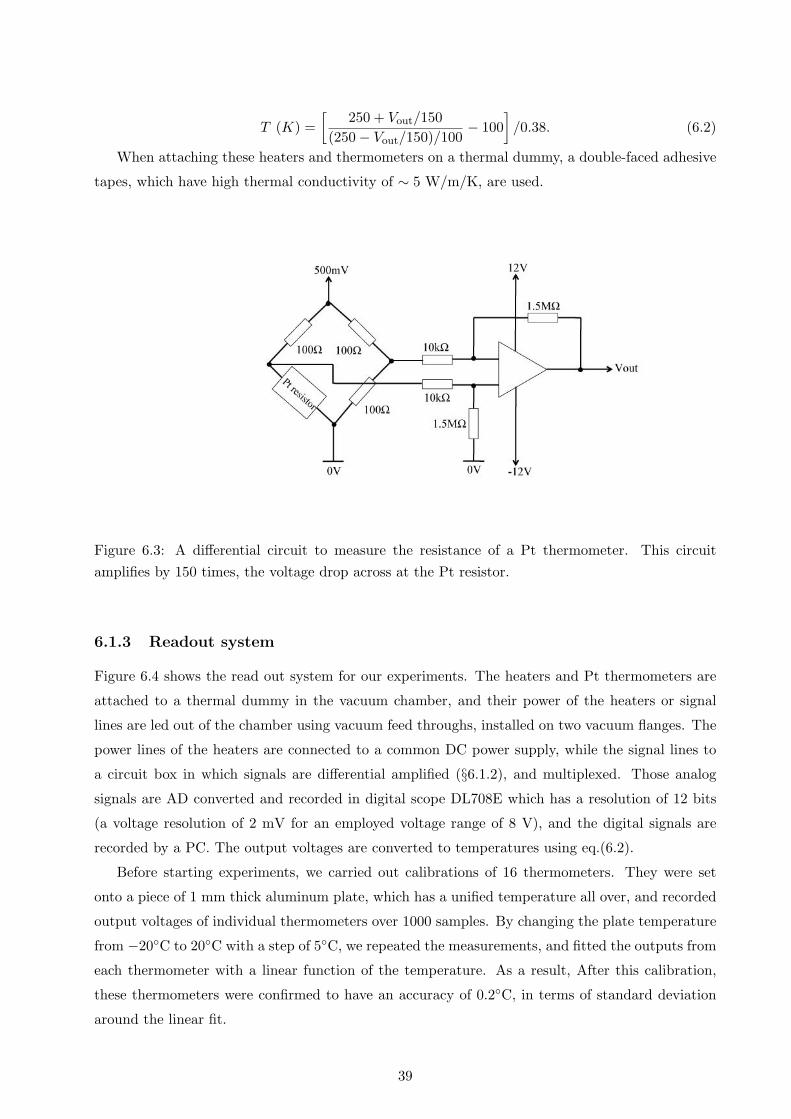
T (K) =[
250 + Vout/150(250 − Vout/150)/100
− 100]/0.38. (6.2)
When attaching these heaters and thermometers on a thermal dummy, a double-faced adhesive
tapes, which have high thermal conductivity of ∼ 5 W/m/K, are used.
Figure 6.3: A differential circuit to measure the resistance of a Pt thermometer. This circuitamplifies by 150 times, the voltage drop across at the Pt resistor.
6.1.3 Readout system
Figure 6.4 shows the read out system for our experiments. The heaters and Pt thermometers are
attached to a thermal dummy in the vacuum chamber, and their power of the heaters or signal
lines are led out of the chamber using vacuum feed throughs, installed on two vacuum flanges. The
power lines of the heaters are connected to a common DC power supply, while the signal lines to
a circuit box in which signals are differential amplified (§6.1.2), and multiplexed. Those analog
signals are AD converted and recorded in digital scope DL708E which has a resolution of 12 bits
(a voltage resolution of 2 mV for an employed voltage range of 8 V), and the digital signals are
recorded by a PC. The output voltages are converted to temperatures using eq.(6.2).
Before starting experiments, we carried out calibrations of 16 thermometers. They were set
onto a piece of 1 mm thick aluminum plate, which has a unified temperature all over, and recorded
output voltages of individual thermometers over 1000 samples. By changing the plate temperature
from −20C to 20C with a step of 5C, we repeated the measurements, and fitted the outputs from
each thermometer with a linear function of the temperature. As a result, After this calibration,
these thermometers were confirmed to have an accuracy of 0.2C, in terms of standard deviation
around the linear fit.
39

Figure 6.4: A readout system of our experiment. There are 16 channels of differential amplifiers.
6.2 Thermal Dummies
In our verification experiments, two thermal dummies are utilized. One of them is a simplified in-
house version, consisting of a piece of graphite sheet, a copper pole, and an aluminum heat sink. Its
photograph is shown in figure 6.5. The heat sink has a size of 120 mm×120 mm×50 mm, to which
the copper pole is connected by a M5 screw torqued at 29.4 kg·f·cm (a standard for satellite-borne
instruments). This simple thermal model is utilized for measurements of the contact conductance
between the graphite sheet and the copper pole.
The other, shown in figure 6.6, is a more faithful thermal dummy, which consists of four copper
poles, a 2 mm thick aluminum electro-magnetic shield box, an aluminum bottom frame, an alu-
minum cold plate, and an aluminum heat sink. The sizes of these components are given in caption
of figure 6.6. These parts are strictly the same in shape as the actual Compton Camera, except
that the legs of the cold plate are 50 mm shorter than those of the actual Compton Camera, due
to limited size of the vacuum chamber (§6.1.1). In order to emulate the Case 2 TMM (§5.3.3),
each copper pole is connected to a side of the aluminum shield wall by thirteen M2 screws, and
connected to the aluminum cold plate by two M5 screws. The bottom frame is connected to the
four sides of the aluminum shield well by four M3 screws (one screw per side), individually, and
connected to the cold plate by eight M5 screws altogether. The aluminum shield is connected to
the cold plate by three M3 screws per side. Finally, the cold plate is connected to the aluminum
heat sink at two sides by ten M5 screws each. These screw settings are visualized in figure 6.10.
This strict thermal model is utilized for verification of the contact conductances by screws.
40

Figure 6.5: A photograph of the simple thermal dummy, emulating the Compton Camera. Apiece of graphite sheet, which has a size of 20 mm×30 mm×0.1 mm, is connected to the copperpole by a double-faced tape with a size of 20 mm×10 mm×0.05 mm. The copper pole, 120 mmtall and 6 × 10 mm2 in cross section, is connected by a M5 screw to the aluminum heat sink(120 mm×120 mm×50 mm).
6.3 Measurement of Conductance between Graphite Sheet and
Copper Pole
6.3.1 Purpose of the experiment
In the TMM for the Compton Camera, the lateral conduction is realized by graphite sheets, which
are connected to the four copper poles. However, the contact conductance between these graphite
sheets and the copper poles is subject to large uncertainties (§5.3.1), and our assumptions employed
in constructing the TMM must be calibrated experimentally. In addition, graphite sheets generally
have highly anisotropic conductivity, which depends on how they are fabricated. Therefore, it is
also important to verify that the particular type of graphite sheet, employed here, can perform as
expected from their catalogued specifications.
6.3.2 Experimental setup
In this experiment, the simple thermal dummy (§6.2) is utilized, in a configuration shown in figure
6.7. The graphite sheet has a width of 20 mm, a length of 30 mm, a thickness of 100 µm, and a
41

Figure 6.6: Top-view (left) and side-view (right) photographs of the more faithful thermal modelof the Compton Camera, which has four copper poles, an aluminum electro-magnetic shield wall,an aluminum bottom frame, an aluminum cold plate, and an aluminum heat sink. The pole hasa size of ∼ 3 mm × 20 mm × 120 mm, the shield has a size of 2 mm×120 mm×120 mm per side,the bottom frame has almost the same size as the tray except for its thickness of 35 mm, the coldplate is 5mm-thick, and the heat sink is 120×240×50 mm3 in size.
conductivity of 700 W/m/K (catalog specification) along its plane. We attached a 100 Ω resistor
(heater) onto one end of the graphite sheet, fix its opposite end to the copper pole with a 50 µm
thick double-faced adhesive tape, with an area of 10 mm×20 mm, and set seven thermometers at
positions indicated in figure 6.7.
After setting the heater and the thermometers, the setup is put into the vacuum chamber, which
is evacuated to a pressure less than 10−3 torr. Then, the 8.9 V voltage is applied to the resistor, as
described in §6.1.3. As also described therein, we record the voltages every 4 sec with a resolution
of 2 mV.
Through this measurement, using eq.(2.6), the heat flow, which runs from the graphite sheet
to the copper pole, can be calculated as
Q = KCu × ∆TCu, (6.3)
where KCu = 0.23 W/K is the conductance of the copper pole, and ∆TCu is its vertical temperature
difference as read from thermometers 5 and 7. We can then calculate the contact conductance K
between the graphite sheet and the copper pole as
K =Q
∆T, (6.4)
where ∆T is the temperature difference between the graphite sheet and the copper pole.
42

Figure 6.7: A setup to measure the contact conductance between a graphite sheet and a copperpole, using the simple thermal dummy. The position of the heater is shown by a red circle, andthose of thermometers by numbers.
In the present experiment, radiative heat flow out of the graphite sheet may not be negligible.
In fact, assuming the graphite to be a perfect radiator (ε = 1) which couples to a black body heat
bath, and assuming a small temperature difference, its radiative conductance is estimated as
KR ∼ 4σT 30 A ∼ 0.006 (W/K) (6.5)
where A = 1000 mm2 is the unobscured graphite surface area (on both sides), and T0 ∼ 300 K is
the ambient temperature (eq. (5.3)). Although this value is not necessarily negligible compared to
KCu and K, eq.(6.3) and eq.(6.4) are considered to be still valid, because Q is the conductive heat
flow along the pole rather than the heater power it self, and because radiative loss from the copper
pole should be much lower because of its low emissivity.
6.3.3 Results
Figure 6.8 (left) shows variations of the temperatures, measured with the 7 thermometers (figure
6.7), while the right shows variations of the temperature differences with respect to the heat sink
(#8). The heater is turned on at 0 sec, and then all the temperatures increase steeply for about
∼ 200 seconds, which is consistent with the heat capacity of the copper pole of 27 J/K. Afterwards,
the temperatures start saturating, and the temperature differences among the 7 thermometers
43

Figure 6.8: (left) Time variations of the temperatures measured by the thermometers indicated infigure 6.7. Red plots (#1) shows the temperature of the heater point, and black shows that of thealuminum heat sink (#8). Green (#3), and blue (#4) are on the graphite sheet, while magenta(#5), cyan (#6), and yellow (#7) are on the copper pole. (right) variations of the temperature inthe form of differences from thatof the heat sink (#8).
Table 6.1: Temperature difference from the thermometer #8 in figure 6.8.Thermometer number ∆T (C) from #8
1 19.63 8.54 4.05 2.46 1.27 0.1
become approximately constant, as shown in figure 6.8 right.
We fitted the data of each thermometer with a straight line, fn(t) = ant + bn (n = 1, 3, · · · , 7 is
number of the thermometers), between 3500 sec and 4500 sec. As a result, an were all found to be
identical within 90% errors, so we employed fn(4500) as the temperature differences. In table 6.1,
we show the temperature differences between the heat sink and the others. The temperature drop
between the top and the bottom parts of the copper pole is 2.4C, so eq. (6.3), yields Q = 0.54 W.
This, together with the measured ∆T = 1.6C across the contact point between the graphite sheet
and the copper pole,
K = 0.34 (W/K). (6.6)
The temperature difference between the positions of thermometers #1 and #3 is 11.1C, so we can
calculate the conductance of the graphite sheet as
44

KG.S. = 0.050 (W/K), (6.7)
also by using eq.(6.4).
6.3.4 Implications of the results
In this experiment, the contact area between the graphite sheet and the copper pole was 200 mm2,
while that in the actual Compton Camera is 24 mm2. Therefore, the actual contact conductance
between the graphite sheet and the copper pole is calculated from eq.(6.6) as,
K =24 (mm2)200 (mm2)
× 0.34 (W/K) = 0.041 (W/K). (6.8)
This value is 80% of value, 0.05 W/K, which we estimated in §5.3.1.
The measured conductance of the graphite sheet is 30% lower than the specification value of
0.070 W/K. However, this is probably due to radiative heat loss from the graphite. In fact, the
heat flow along the pole, Q = 0.54 W, is lower by ∼30% from the applied heat input, 0.80 W.
The difference, ∼0.2 W, can be attributed to radiation, approximately because eq.(6.5) predicts
E ∼ 0.12 W for ∆T = 20C.
Figure 6.9: TD reproduction of the present experiment, including the effect of radiation. See textfor the condition of simulation.
To reproduce the measurement considering radiation from the surface of the dummy,we carried
out a TD calculation including radiation. The contact conductance between the graphite sheet and
45

the copper pole is 0.34 W/K, as obtained in §6.3.4. The boundary temperature at the bottom part
of the copper pole is set 22C, and that of the vacuum chamber 20C. The emissivity of copper pole
was assumed to be 0.05, while that of graphite sheet to be 1.0. Figure 6.9 shows the result. The
calculated temperature distribution well reproduces our experimental result, and the temperature
difference between the top and the bottom parts of the copper pole is 2.6C. The calculated heat
flow in the copper pole is 0.6 W, so rest 0.2 W (∼ 30% of all) is radiated.
6.4 Verification of Screw Contact Conductance
IIn order to measure contact conductances due to screws, we performed an experiment, which is
similar to that in §6.4, but using the faithful dummy.
6.4.1 Experimental setup
Figure 6.10: A 3D CAD picture of the more faithful thermal dummy of the Compton Camera. Thepositions of the heaters are shown by red circles, and those of the thermometers by numbers.
In the present experiment, the more faithful thermal model of the Compton Camera (§6.2) is
used, As shown in figure 6.10, four heaters were attached directly to the top of the four copper
poles, and 7 thermometers were arranged on one side of the dummy; #1 (heater point), #6, and
#7 are on the pole; #3, #4, #5 are on the aluminum shield wall; #8 on the cold plate. The rest
46

of the experiment is the same as performed in §6.3.
6.4.2 A result of the experiment
Figure 6.11: (left) Variations of the temperatures of the faithful dummy, measured by the ther-mometers indicated in figure 6.10. Red (#1) shows the temperature of the heater point, and black(#8) that of the cold plate. Green (#3), blue (#4) and purple (#5) are on the aluminum shieldwall, while cyan (#6) and yellow (#7) are on the copper pole. (right) Temperature differencesfrom the cold plate (#8).
Table 6.2: Temperature difference from thermometer #8 in figure 6.11.Thermometer number ∆T (C) from #8
1 1.9 − 2.4 (our best estimation 2.1)3 0.94 0.95 0.66 0.77 0.2
Figure 6.11 left shows variations of the 7 temperatures of figure 6.10. The temperatures behave
in a similar manner to figure 6.8, except that the gradual increase (after ∼500 sec) is steeper
because 4 heaters, instead of one, were used.
The temperature of the thermometer #7 (yellow) does not become parallel to the others until
∼ 4000 sec, because the cold plate touches the heat sink directly, and its temperature variation
is influenced by that of the heat sink which has a large heat capacity of ∼ 3800 J/K. Applying a
linear fit to these data traces over t = 5000− 6000 sec, just as we did in §6.3.3, we determined the
temperatures at t = 6000 sec. In table 6.2, we summarize the temperature differences between the
cold plate (#8) and the others.
The temperature of the thermometer #1 (red) increases in parallel to the others (except for
47

#7) until 2000 sec. However, between 2000 sec and 6000 sec, its slope became ∼10% smaller than
those of the others, and f1(6000)− f8(6000) = 1.9C is considered to be underestimated. Actually,
when we perform the fitting over 1000 − 2000 sec, the result became f1(6000) − f8(6000) = 2.4C,
which would be an overestimation. Therefore, we decided to use #3 as a relay point; fitting over
1000 − 2000 sec gives f1(2000) − f3(2000) = 1.2C. Adding it to the that between #3 and #8 in
a range of 5000 sec and 6000 sec, i.e., f3(6000) − f8(6000) = 0.9C (table 2), we obtain the more
reasonable value of 2.1C (the value in brackets in table 6.2). This value is utilized to estimate the
contact conductances in next subsection.
6.4.3 Implications of the results
we constructed another TMM which simulate the faithful dummy, and calculated the temperature
distributions as we change the screw-contact conductances. Comparing the experimental results
with the simulations, we can find the best estimates of the contact conductances.
Figure 6.12: A TD-calculated temperature distribution of the faithful dummy, when we put 0.8 Wheat into a top of the copper pole. This is based on a TMM meant to reproduce the faithful dummy(§6.4.2).
Figure 6.12 shows the temperature distribution simulated by our new TMM (§6.4.2), when
the contact conductances are the same as our assumption in §5.2. It shows that the temperature
difference between the top of the copper pole and the cold plate is 3.7C, and which is higher than
the experimental value, 2.1C. This means that we over-estimated the contact conductances.
48

Figure 6.13: The simulated relation between the contact conductances and the temperatures on themore faithful dummy. The unit of the horizontal axis is the screw contact conductance, expressedin its ratio to the value assumed in eq. (5.4).
We repeated the TD calculation by changing the contact conductances, and show in figure 6.13
the predicted temperatures as a function of the contact conductances. Comparing the experimental
results (table 6.2) with the results of the sensitivity analysis (figure 6.13), we fine that the actual
screw contact conductances should be ∼4 times larger than the worst case of eq.(5.4) which we
assumed in the TMM in §5.2.4. This factor 4 difference appears reasonable from figure 5.3, where
the other estimates are larger by a factor of 1.5 to 10 than eq.(5.4).
However, all of the experimental temperatures of aluminum shield well are smaller than esti-
mated ones by 0.2C. This is considered to be because the large area not pressed by screws are
contact to the cold plate, and heat is conducted there.
6.5 Calibration of TMM
In §6.4, the contact conductance between the graphite sheet and the copper pole is confirmed to
be 0.04 W/K, On the other hand, the actual contact conductances by screws are estimated to
be four times larger than our assumption, eq.(5.4). Including these actual measurement values
into the TMM, the temperature distribution in the actual Compton Camera was re-calculated.
Figure 6.14 shows the result of the calculation, using this “calibrated” TMM. We confirm that
the temperature of the top Si semi-conductor is −16.0C, which fulfills the thermal requirements.
Figure 6.15 summarizes the predictions of the calibrated TMM.
Although our experiment indicated a significantly better contact conductance for screws, the
49

result in table 6.2 is obviously subject to systematic errors. If, e.s., we take ∆T = 2.4C between
#1 and #8, the implied contact conductance is only twice larger than eq.(5.4). Therefore, we
represented the TMM calculation, and formed that the top semi-conductor becomes −15.5C.
Therefore, our conclusion remains unaffected by these systematic errors.
Figure 6.14: A temperature distribution calculated by the calibrated TMM. In this model, thecontact conductance between the graphite sheet and the copper pole is 0.05 W/K, and the contactconductances by screws are four times larger than our original assumption.
50

Figure 6.15: The same as figure 5.11, but using the calibrated TMM.
51

Chapter 7
CONCLUSION
In the present thesis, we developed, both numerically and experimentally, the thermal design of the
Compton Cameras, which work as the main detectors of the Soft Gamma-ray Detector onboard
ASTRO-H. Our main objective is how to reduce the anticipated vertical temperature gradient, and
hence to make the temperature of the Compton Camera lower than −15C from top to bottom.
We suggested to put graphite sheets under every ASIC to distance heat from semi-conductor
devices in lateral direction, and four copper poles which go through all layers and carry heat
generated at them to the cold plate in vertical direction. In addition, an electro-magnetic shield
wall and a bottom frame can also be utilized as effective heat paths.
To verify the effects of these new heat paths, we constructed a thermal mathematical model
(TMM), and calculated the temperature distributions in the Compton Camera. In this calculation,
we assumed the thermal contact conductances at all contact points, related with the sizes of screws
and a double faced tape which are utilized there. As a result, the new thermal components were
found to fulfill the thermal requirements. However, the TMM has systematic errors arising from
uncertainties in the assumed the thermal contact conductances.
We prepared two thermal dummies; one is to verify the thermal contact conductance between
the graphite sheet and the copper pole, by double faced tape, and the other is to verify those between
metals, by screws. Then, we carried out the verification experiments in a vacuum chamber. As a
result, the contact conductance by double faced tape, was confirmed to be almost the same as our
assumption. Those by screws, were estimated to be four times as large as our assumptions.
Utilizing these contact conductance values obtained in the experiments, we calibrated TMM,
and re-calculated the temperature distribution of the actual Compton Camera. As a result, we
succeeded in keeping the temperatures of the all layers between −16C and −20C. Therefore,
our thermal design of the Compton Camera including the new heat paths which we suggested are
verified to fulfill the thermal requirements.
52

Bibliography
[1] Aya Kubota Master’s Thesis, “Thermal Design and Verification of The Hard X-ray Detector
for ASTRO-E” (The University of Tokyo, 1998)
[2] Spacecraft Thermal Control Handbook, Volume I: Fundamental Technologies, David G. Gilmore
Editor
[3] Anon., “Thermal Environments” in TRW, Inc. Project MILSTAR Engineering Design Stan-
dards, Section 2.2, March 1984.
[4] George D. Rhoads, informal data transmittal, 1990.
[5] Tim Panzak,The Finite Element Method and Thermal Desktop, Cullimore and Ring Technolo-
gies
[6] JSME text series “Heat Transfer” (The Japan Society of Mechanical Engineers)
[7] H.Noda et al. (2011), PASJ, in press
53
Acknowledgement
I would like to express my thank all the people who have supported my graduate student life. Espe-
cially, I am grateful to the Professor Makishima to his supports and advices to my study. Without
his help, I could not complete this theses. Hereafter, I hope to learn more about astrophysics and
experimental physics from him.
I would like to thank Lecturer Nakazawa who taught me how the satellite-borne instruments
are made. Many discussions with him made me interested in designing such instruments.
I would like to give special thanks to my parents, my brothers, my colleagues, my friends, and
Ayaka Morita who strongly supported me any time in my graduate school life.
54