Embed Size (px)
Citation preview

Theory of Modern Electronic Semiconductor DevicesKevin F. Brennan and April S. Brown
Copyright c! 2002 John Wiley & Sons, Inc.ISBNs: 0-471-41541-3 (Hardback); 0-471-22461-8 (Electronic)
CHAPTER 1
Overview of Semiconductor Device Trends
The dawn of the third millennium coincides with what has often been referredto as the information age. The rapid exchange of information in its variousformats has become one of the most important activities of our modern world.Shannon’s early recognition that information in its most basic form can bereduced to a series of bits has lead to a vast infrastructure devoted to therapid and efficient transfer of information in bit form. The technical devel-opments that underlie this infrastructure result from a blending of computingand telecommunications. Basic to these industries is semiconductor hardware,which provides the essential tools for information processing, transfer, anddisplay.
1.1 MOORE’S LAW AND ITS IMPLICATIONS
The integrated circuit is the fundamental building block of modern digitalelectronics and computing. The rapid expansion of computing capability isderived mainly from successive improvements in device miniaturization andthe concomitant increase in device density and circuit complexity on a singlechip. Functionality per chip has grown in accordance with Moore’s law, anhistorical observation made by Intel executive Gordon Moore. Moore’s lawstates that functionality as measured by the number of transistors and bitsdoubles every 1.5 to 2 years. As can be seen from Figure 1.1.1, the numberof transistors on a silicon chip has followed an exponential dependence sincethe late 1960s. This in turn has led to dramatic improvements in computingcapability, leading the consumer to expect ever better products at reduced cost.
1

2 OVERVIEW OF SEMICONDUCTOR DEVICE TRENDS
FIGURE 1.1.1 Number of transistors per chip as a function of year, including thenames of the processors. The dashed line shows projections to 2010. The exponentialgrowth reflected by this graph is what is commonly referred to as Moore’s law. (Datafrom Birnbaum and Williams, 2000.)
One of the questions that this book addresses is: Is there a limit to Moore’slaw? Can integrated-circuit complexity continue to grow exponentially intothe twenty-first century, or are their insurmountable technical or economicchallenges that will derail this progress?
The two prominent technical drivers of the semiconductor industry are dy-namic random access memory (DRAM), and microprocessors. Historically,DRAM technology developed at a faster pace than microprocessor technol-ogy. However, from the late 1990s microprocessors have become at least anequal partner to DRAMs in driving semiconductor device refinement. In manyinstances, microprocessor units (MPUs), have become the major driver ofsemiconductor technology. There are different performance criteria for thesetwo major product families. The major concerns for DRAMs are cost andmemory capacity. The usual metric applied to DRAMs is half-pitch, which isdefined as essentially the separation between adjacent memory cells on thechip. Consequently, minimization of the area of each memory cell to pro-vide greater memory density is the primary development focus for DRAMs.Cost and performance also drive microprocessor development, but the key pa-rameters in this case are gate length and the number of interconnect layers.The maintainence of Moore’s law requires, then, aggressive reduction in gatelength as well as in DRAM cell area.
The semiconductor industry has tracked the technology trends of bothDRAM and microprocessor technology and established technology road mapsto project where the technology will be in subsequent years. Such road mapsprovide the industry with a rough guide to the technology trends expected.Below we discuss some of the implications of these trends and examine howthey affect Moore’s law.

MOORE’S LAW AND ITS IMPLICATIONS 3
FIGURE 1.1.2 Fabrication plant cost as a function of year. Notice the tremendouscost projected by the year 2010. (Data from Birnbaum and Williams, 2000.)
Let us first consider economic challenges to the continuation of Moore’slaw. There is a second law attributed to Moore, Moore’s second law, whichexamines the economic issues related to integrated-circuit chip manufacture.According to Moore’s second law, the cost of fabrication facilities needed tomanufacture each new generation of integrated circuits increases by a factorof 2 every three years. Extrapolating from fabrication plant costs of about $1billion in 1995, Figure 1.1.2 shows that the cost of a fabrication plant in 2010could reach about $50 billion. That a single company or even a consortiumof companies could bear such an enormous cost is highly doubtful. Even ifa worldwide consortium of semiconductor industries agreed to share such acost, continuing to do so for future generations would certainly not be feasi-ble. Therefore, it is likely that the economics of manufacturing will stronglyinfluence the growth of the integrated-circuit industry in the near future.
Aside from the economic issues faced by continued miniaturization, severaldaunting technical challenges threaten continued progress in miniaturizationof integrated circuits in accordance with Moore’s law. As discussed in detailin Chapter 7, several technical issues threaten continued exponential growthof integrated-circuit complexity. Generally, these concerns can be classified aseither physical or practical. By physical challenges we mean problems encoun-tered in the physical operation of a device under continued miniaturization.Practical challenges arise from the actual fabrication and manufacture of theseminiaturized devices. Among the practical challenges are lithography, gateoxide thickness reduction, and forming interconnects to each device. Physicaloperational problems encountered by continued miniaturization of devices in-clude threshold voltage shifts, random fluctuation in the dopants, short-channeleffects, and high-field effects. Any one or a combination of these effects couldthreaten continued progress of Moore’s law. We examine these effects in detailin Chapter 7.

4 OVERVIEW OF SEMICONDUCTOR DEVICE TRENDS
FIGURE 1.1.3 Number of chip components as a function of device feature size. Boththe historical trend and projected values according to the Semiconductor Institute ofAmerica (SIA) road map are shown. (Data from Birnbaum and Williams, 2000.)
Figure 1.1.3 shows how the number of chip components scales with theon-chip feature size. As can be seen, to maintain the historical trend in thenear future, device feature sizes will need to be scaled significantly below0:1 ¹m. However, doing so requires overcoming many of the challenges listedabove. At the time of this writing, strategies for overcoming the physical andpractical challenges to further miniaturization are not known.
In addition to the practical and physical challenges to continued miniatur-ization, there are other issues that may thwart further progress. Formidablechallenges arise in design, testing, and packaging integrated circuits contain-ing billions of transistors. For example, testing a chip containing billions oftransistors that operates at gigabit speeds is presently not possible. It is not suf-ficient that the chip contain billions of devices and operates at gigabit speeds.Just as important is the ability to extract signals from the transistors within thechip at gigahertz frequencies. Therefore, new packaging schemes will need tobe developed to ensure that chip output progresses along with the chip itself.
Although there are many practical and physical challenges that may thwartfurther reduction of integrated circuits, progress may still occur through ei-ther evolutionary or revolutionary advancements. By evolutionary, we meancontinued progress in device reduction through progressive refinements in themain integrated-circuit technology itself, complementary metal-oxide semi-conductor (CMOS), technology. In Chapter 7 we examine several evolutionarytechnologies that could potentially extend CMOS in accordance with Moore’slaw. Alternatively, revolutionary technologies that go well beyond conventionalCMOS may be required to continue progress in miniaturization. In Chapter8 we examine several leading candidate technologies that may form the ba-sis of computing hardware in the future. However, before anyone begins toinvest and develop these alternative technologies aggressively, it is first nec-
MOORE’S LAW AND ITS IMPLICATIONS 5
essary to examine just how much better computing hardware can be made tobe. It would be very unwise to pursue an expensive revolutionary technologyaggressively if only marginal performance improvements can be made.
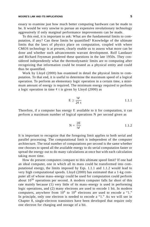
To this end, it is important to ask: What are the fundamental limits to com-putation, if any? Can these limits be quantified? Knowledge of the ultimatelimits that the laws of physics place on computation, coupled with whereCMOS technology is at present, clearly enable us to assess what more can bedone and whether such advancements warrant development. Rolf Landauerand Richard Feynman pondered these questions in the late 1950s. They con-sidered independently what the thermodynamic limits are to computing afterrecognizing that information could be treated as a physical entity and couldthus be quantified.
Work by Lloyd (2000) has examined in detail the physical limits to com-putation. To that end, it is useful to determine the maximum speed of a logicaloperation. To perform an elementary logic operation in a certain time, a mini-mum amount of energy is required. The minimum energy required to performa logic operation in time ¢t is given by Lloyd (2000) as
E " ¼¹2¢t
1.1.1
Therefore, if a computer has energy E available to it for computation, it canperform a maximum number of logical operations N per second given as
N =2E
¼¹1.1.2
It is important to recognize that the foregoing limit applies to both serial andparallel processing. The computational limit is independent of the computerarchitecture. The total number of computations per second is the same whetherone chooses to spend all the available energy to do serial computation faster orspread the energy out to do many calculations at once but with each calculationtaking more time.
How do present computers compare to this ultimate speed limit? If one hadan ideal computer, one in which all its mass could be transformed into com-putational energy, the limits imposed by Eqs. 1.1.1 and 1.1.2 would lead tovery high computational speeds. Lloyd (2000) has estimated that a 1-kg com-puter all of whose mass–energy could be used for computation could performabout 1050 operations per second. A modern computer falls far short of thisrate mainly because (1) very little of its mass–energy is used in performinglogic operations, and (2) many electrons are used to encode 1 bit. In moderncomputers, anywhere from 106 to 109 electrons are used to encode a “1.”In principle, only one electron is needed to encode a “1.” As we will see inChapter 8, single-electron transistors have been developed that require onlyone electron for charging and storage of a bit.

6 OVERVIEW OF SEMICONDUCTOR DEVICE TRENDS
In addition to the limit placed on the computational speed of a logicaloperation, thermodynamics limits the number of bits that can be processedusing a specific amount of energy in a given volume. The amount of availableenergy limits the computational rate, while the entropy limits the amount ofinformation that can be stored and manipulated. The classical entropy is relatedto the multiplicity of states as (Brennan, 1999, Sec. 5.3)
S = kB¾ = kB lng 1.1.3
where kB is Boltzmann’s constant, ¾ the entropy, S the conventional entropy,and g the multiplicity function. For a two-level system of m components,the multiplicity function g is equal to 2m. Such a system can store m bits ofinformation. Thus the number of bits m that can be stored in the system canbe related to the entropy as
m =S
kB ln21.1.4
Combining Eqs. 1.1.2 and 1.1.4, the maximum number of logical operationsper second per bit can be found as
operationsbit-second
=2E
¼¹kB ln2
S=
2EkB ln2¼¹S
1.1.5
Recognizing that the temperature T is given as (Brennan, 1999, Sec. 5.3)
1T
=dS
dE1.1.6
the maximum number of operations per bit per second can be approximatedas
operationsbit-second
# kBT
¹1.1.7
Thus the temperature limits the maximum number of operations per bit persecond. A very high temperature is needed to maximize the number of op-erations. High-temperature operation is undesirable in a practical computingsystem.
In summary, the thermodynamic limit of a nonreversible computer (one inwhich there exists dissipation of energy during computation) is many orders ofmagnitude higher than the estimated upper limit of CMOS circuitry. Based onthese results, it is clear that there remains the possibility of a huge improvementin computing capability with further miniaturization. Although different pathsmay need to be taken from the current one for CMOS, there remains the strongpossibility that dramatic improvement in computing hardware can be realizedwith increased miniaturization. Part of the focus of this book is to examinewhat technologies can be harnessed to provide further miniaturization.

SEMICONDUCTOR DEVICES FOR TELECOMMUNICATIONS 7
1.2 SEMICONDUCTOR DEVICES FOR TELECOMMUNICATIONS
Although the largest part of the semiconductor industry is devoted to sili-con integrated-circuit technology and CMOS in particular, the rapid growthof the telecommunications industry has stimulated significant growth in a dif-ferent part of the semiconductor industry: compound semiconductors. Thetotal worldwide semiconductor market has exceeded $200 billion in sales inthe year 2000. Only about $15 billion of this amount can be attributed tocompound semiconductor products. Nevertheless, compound semiconductorshave undergone a dramatic increase in sales over the past decade. From theearly to late 1990s, shipment of compound semiconductor device productshas increased over fourfold. Much of the rapid growth in compound semicon-ductor products has occurred in telecommunications, owing to expansion inboth wireless and wired fiber-optic systems. Projections indicate that due tothe rapid growth of the telecommunications industry, the sale of compoundsemiconductor products will grow more rapidly than that of silicon-basedsemiconductor products.
The most important compound semiconductor products used in fiber-opticnetworks are optoelectronic devices, particularly lasers and detectors. Semi-conductor lasers are made exclusively from compound semiconductors sincethese materials have direct bandgaps and can thus be made to lase. In con-trast, silicon is an indirect-gap semiconductor and currently cannot lase. Inaddition, direct-gap materials make more efficient photodetectors, at least forradiation with wavelengths near the bandgap. For these reasons, the opto-electronic component industry utilizes primarily compound semiconductors.Although the overall market for optoelectronic devices is small compared tothat for CMOS, it is still substantial. Revenue in 2000 for optical componentsexceeded $10 billion. Forecasts predict that the worldwide optical componentmarket will exceed $19 billion by 2003, just about doubling in three to fouryears. In this book we restrict our discussion to electronic devices and do notconsider optoelectronic devices. The interested reader is referred to the bookby Brennan (1999) for a discussion of optoelectronic devices.
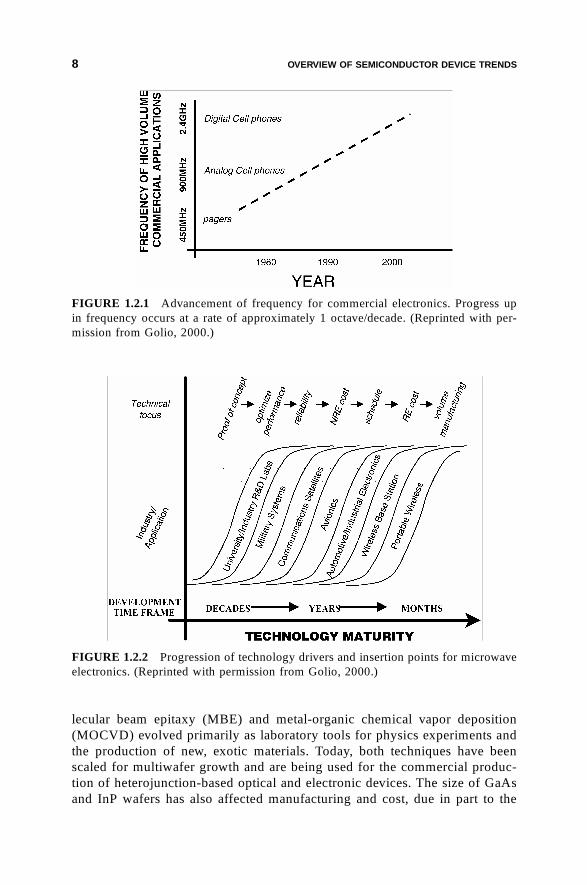
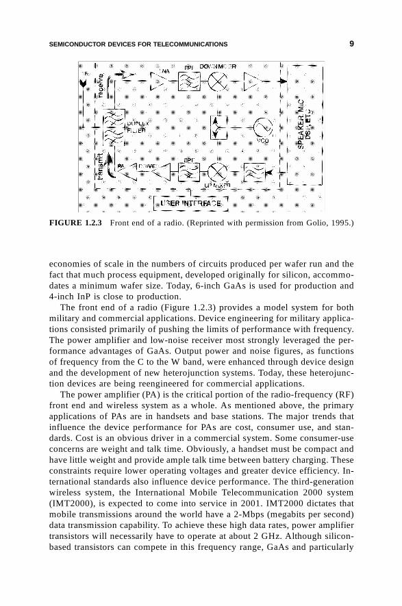
The compound semiconductor industry developed from military electron-ics needs for microwave and millimeter-wave systems. For these applications,including radar and satellite-based communications, cost was considered asecondary metric to performance. With the advent of microwave commer-cial electronics, the metrics have changed. Figure 1.2.1 shows the increasein frequency for commercial electronics over the past two decades. Figure1.2.2 shows the progression of technology drivers and insertion points for mi-crowave electronics. The movement toward commercial electronics has signifi-cantly reduced the cycle time, placed a much stronger emphasis on ruggednessor reliability, and broadened the scope of relevant and specific performancecriteria.
Advances in epitaxy, the process technique for producing atomically smoothheterojunctions, have, in part, enabled their use in commercial products. Mo-
8 OVERVIEW OF SEMICONDUCTOR DEVICE TRENDS
FIGURE 1.2.1 Advancement of frequency for commercial electronics. Progress upin frequency occurs at a rate of approximately 1 octave/decade. (Reprinted with per-mission from Golio, 2000.)
FIGURE 1.2.2 Progression of technology drivers and insertion points for microwaveelectronics. (Reprinted with permission from Golio, 2000.)
lecular beam epitaxy (MBE) and metal-organic chemical vapor deposition(MOCVD) evolved primarily as laboratory tools for physics experiments andthe production of new, exotic materials. Today, both techniques have beenscaled for multiwafer growth and are being used for the commercial produc-tion of heterojunction-based optical and electronic devices. The size of GaAsand InP wafers has also affected manufacturing and cost, due in part to the
SEMICONDUCTOR DEVICES FOR TELECOMMUNICATIONS 9
FIGURE 1.2.3 Front end of a radio. (Reprinted with permission from Golio, 1995.)
economies of scale in the numbers of circuits produced per wafer run and thefact that much process equipment, developed originally for silicon, accommo-dates a minimum wafer size. Today, 6-inch GaAs is used for production and4-inch InP is close to production.
The front end of a radio (Figure 1.2.3) provides a model system for bothmilitary and commercial applications. Device engineering for military applica-tions consisted primarily of pushing the limits of performance with frequency.The power amplifier and low-noise receiver most strongly leveraged the per-formance advantages of GaAs. Output power and noise figures, as functionsof frequency from the C to the W band, were enhanced through device designand the development of new heterojunction systems. Today, these heterojunc-tion devices are being reengineered for commercial applications.
The power amplifier (PA) is the critical portion of the radio-frequency (RF)front end and wireless system as a whole. As mentioned above, the primaryapplications of PAs are in handsets and base stations. The major trends thatinfluence the device performance for PAs are cost, consumer use, and stan-dards. Cost is an obvious driver in a commercial system. Some consumer-useconcerns are weight and talk time. Obviously, a handset must be compact andhave little weight and provide ample talk time between battery charging. Theseconstraints require lower operating voltages and greater device efficiency. In-ternational standards also influence device performance. The third-generationwireless system, the International Mobile Telecommunication 2000 system(IMT2000), is expected to come into service in 2001. IMT2000 dictates thatmobile transmissions around the world have a 2-Mbps (megabits per second)data transmission capability. To achieve these high data rates, power amplifiertransistors will necessarily have to operate at about 2 GHz. Although silicon-based transistors can compete in this frequency range, GaAs and particularly

10 OVERVIEW OF SEMICONDUCTOR DEVICE TRENDS
heterojunction-based electronics generally offer lower noise and improved lin-earity.
Heterojunction device engineering requires much stronger coupling to sys-tem requirements. An example is in the design for high linearity in poweramplifiers. As shown in Chapter 3, linear HFETs can be designed throughcontrol of the doping profile or by choosing an enhancement-mode device asopposed to a depletion-mode device. HBT collector thicknesses and dopingprofiles strongly affect linearity, as discussed in Chapter 4. Specific linearityrequirements, in turn, are determined by the specific standard and associatedmodulation format. Thus, the new device engineer must clearly understandthe context of the device in the system specification.
The major challenges that next-generation wireless systems face are prop-agation loss, shadowing, and multipath fading. Propagation loss arises fromreflection and scattering. The loss is proportional to the square of the fre-quency and the distance to the nth power, where n is 2 for free space, 4.35 forrural open space, and 3 to 4.3 for urban/suburban space. Objects such as autosor a building that temporarily block the base station and the receiver causeshadowing. Multipath fading arises when signals are received after havingtaken multiple routes. Multipath fading can cause distortion, which can leadto a significant increase in the bit-error rate. The most promising approachesto combating multipath fading are orthogonal frequency-division multiplexing(OFDM) and code-division multiple access (CDMA). OFDM employs mul-ticarriers for one channel in place of a single carrier. The original signal isdivided into many narrow bandwidths and sent by a different carrier with adifferent frequency. CDMA utilizes a spread spectrum to obtain frequency di-versity. One of the principal operating requirements of the power amplifiersused in these systems is linearity. Why is linearity of a power amplifier soimportant? Nonlinearity in a output of the power amplifier leads to powerleakage out of the signal channel into adjacent channels. Adjacent channelleakage is caused by third-order intermodulation distortion, which is inter-modulation distortion between the fundamental and second harmonic signals.
An additional system constraint results from the current packaging of in-tegrated circuits into modules for RF applications. A mixture of Si circuitsand GaAs circuits is common for front-end components. Clearly, a single ma-terial and circuit technology will lead to lighter and more compact circuitsand therefore systems. However, each specific material and device technologyoffers specific advantages and disadvantages. SiGe technology offers the ad-vantages of heterojunction design to Si technology but cannot address the RFlimitations of the conducting Si substrate. The conducting substrate introducessignificant signal loss, as the frequency is increased and therefore limits Si asa monolithic microwave integrated circuit (MMIC). Figure 1.2.4 shows theperformance of three technologies—Si BJT, HBT, and HEMT—as a functionof metrics. Each metric is relevant to performance in a different block of afront end. An ultimate solution to this problem is heterogeneous integration ofdissimilar materials and devices. Advanced materials and process technology

DIGITAL COMMUNICATIONS 11
FIGURE 1.2.4 Performance of three device technologies—Si BJT, HBT, and HEMT—as a function of performance metrics. (Reprinted with permission from Honjo, 1997.)
will offer this option. Figure 1.2.5 shows an integrated circuit comprised oftwo different device types, HEMTs and HBTs, integrated laterally by selec-tive area epitaxy. Other approaches include wafer bonding or device/circuitpick-and-place integration.
1.3 DIGITAL COMMUNICATIONS
The primary driver of the communications industry in the foreseeable future isthe ever-growing demand for the rapid, efficient, and accurate transfer of digi-tal information. The recognition that all information can ultimately be digitizedmakes it possible to convey it through telecommunications systems. Amongthe many formats of digital information are voice, audio (music, radio, etc.),visual (photos, television, movies, newspapers, etc.), and computer informa-tion. All of these formats are either presently being transmitted or planned fortransmission via the Internet, wireless, and fiber-optic telephone networks. Asa result, telecommunications and computing are blending together.
One of the major issues that confronts telecommunications/computing tech-nology is what conditions will be required of the hardware in fiber-optic andwireless systems that will ensure very high bandwidth communications at alow bit-error rate in the future. Feature size is one of the most important

12 OVERVIEW OF SEMICONDUCTOR DEVICE TRENDS
FIGURE 1.2.5 Integration of dissimilar device types: HEMTs and HBTs. (Reprintedwith permission from Dwight Streit, TRW.)
parameters that dictates high-speed device performance. In addition, the stor-age of massive amounts of data for rapid retrieval, transmission, and pro-cessing requires very small memory devices. Therefore, in both digital andanalog electronics, the major drive is for continued miniaturization, since itprovides faster device operation and denser integrated circuits for memoryand processing applications. Continued miniaturization will place device per-formance squarely within the quantum regime, wherein the device physics isgoverned primarily by quantum mechanical effects.
Quantum devices can be classified as structures with feature sizes compa-rable to or less than the electron de Broglie wavelength or devices in whichcharge quantization dominates the device physics. The de Broglie wavelengthin semiconductors is less than 100 nm. Devices with feature size dimensions(i.e., gate lengths, well widths, etc.) below about 100 nm, then, will generallyexhibit quantum effects. Inspection of Figure 1.1.3 shows that device sizeswill be below 100 nm and begin to exhibit quantum effects in the near futureif Moore’s law continues.
Highly dense memory chips will require very small half-pitch, whereinfew electrons will be used to store a bit. Single-electron transistors, devicesin which a single-electron represents a bit, have already been made. Memorychips comprised of single-electron transistors offer very high density randomaccess memory that can conceivably store vast amounts of digital information.
Quantum devices need not necessarily be made of semiconductors. Newelectronic devices have been made using molecules, leading to the new fieldof moletronics. The particular attraction of molecules for device developmentis that they are naturally three-dimensional, thus providing massive devicedensities. In addition, many molecules are self-replicating, leading to the in-teresting possibility that computers could be self-made. In this book we discuss
DIGITAL COMMUNICATIONS 13
the workings of various types of quantum devices and examine their possibleuse in future digital and analog electronics.
The book is organized as follows. In Chapters 2 to 4 we focus on conven-tional (defined as operating semiclassically), yet state-of-the-art devices basedon heterostructures, heterostructure field-effect transistors (HFETs), and het-erostructure bipolar transistors (HBTs). The physics of the transferred electroneffect, in both k and real space, along with their concomitant devices, is pre-sented in Chapter 5. In Chapter 6 we examine quantum mechanical devicesbased on resonant tunneling as well as the physics of resonant tunneling.The challenges to CMOS and both evolutionary and revolutionary alternativesto CMOS are examined in Chapters 7 and 8. The revolutionary alternativeswe examine include quantum dot cellular automata, single-electron transis-tors, moletronics, and defect-tolerant computing. The book concludes with adiscussion of magnetic field effects in semiconductors, including integer andfractional quantum Hall effects, which may affect futuristic devices.