Embed Size (px)
Citation preview

Journal of Instrumentation
OPEN ACCESS
``The Read-Out Driver ROD card for theInsertable B-layer (IBL) detector of the ATLASexperiment commissioning and upgrade studiesfor the Pixel Layers 1 and 2To cite this article G Balbi et al 2014 JINST 9 C01044
View the article online for updates and enhancements
You may also likePotential impacts of 15 degC and 2 degC globalwarming on rainfall onset cessation andlength of rainy season in West AfricaNaomi Kumi and Babatunde J Abiodun
-
A PCIe DAQ board prototype for PixelDetector in high energy physicsL Lama G Balbi D Falchieri et al
-
Modeling of cellular response after FLASHirradiation a quantitative analysis basedon the radiolytic oxygen depletionhypothesisHongyu Zhu Junli Li Xiaowu Deng et al
-
This content was downloaded from IP address 17657654 on 27022022 at 0650
2014 JINST 9 C01044
PUBLISHED BY IOP PUBLISHING FOR SISSA MEDIALAB
RECEIVED November 14 2013ACCEPTED December 17 2013
PUBLISHED January 23 2014
TOPICAL WORKSHOP ON ELECTRONICS FOR PARTICLE PHYSICS 201323ndash27 SEPTEMBER 2013PERUGIA ITALY
ldquoThe Read-Out Driverrdquo ROD card for the InsertableB-layer (IBL) detector of the ATLAS experimentcommissioning and upgrade studies for the PixelLayers 1 and 2
G Balbia M Bindia SP Chenb D Falchieric T Flickd A Gabriellic S Hauckb
SC Hsub M Kretze A Kugele L Lamac P Morettini f R Travaglinia1
and M Wensingd
aINFN mdash Sezione di Bolognavle B Pichat 62 Bologna Italy
bUniversity of Washington3910 15th Ave NE Seattle WA USA
cUniversity of Bologna amp INFN Bolognavle B Pichat 62 Bologna Italy
dFachbereich C Physik WuppertalGauss-str 20 Wuppertal Germany
eUniversity of HeidelbergZITIB6 26 Mannheim Germany
f INFN mdash Sezione di Genovavia Dodecaneso 33 Genova Italy
E-mail RiccardoTravagliniboinfnit
ABSTRACT The upgrade of the ATLAS experiment at LHC foresees the insertion of an innermostsilicon layer called the Insertable B-layer (IBL) The IBL read-out system will be equipped withnew electronics The Readout-Driver card (ROD) is a VME board devoted to data processingconfiguration and control A pre-production batch has been delivered for testing with instrumentedslices of the overall acquisition chain aiming to finalize strategies for system commissioning Inthis paper system setups and results will be described as well as preliminary studies on changesneeded to adopt the ROD for the ATLAS Pixel Layers 1 and 2
KEYWORDS Data acquisition circuits Detector control systems (detector and experiment moni-toring and slow-control systems architecture hardware algorithms databases) Digital electroniccircuits
1Corresponding author
ccopy CERN 2014 published under the terms of the Creative Commons Attribution 30License by IOP Publishing Ltd and Sissa Medialab srl Any further distribution of this
work must maintain attribution to the author(s) and the published articlersquos title journal citation and DOIdoi1010881748-0221901C01044
2014 JINST 9 C01044
Contents
1 Introduction 111 The ATLAS Pixel detector and the Insertable Barrel Layer (IBL) for the upgrade
phase-0 112 Overview of the IBL readout electronics 213 The Read-Out Driver (ROD) card 2
2 The ROD production and commissioning 321 Prototyping pre-production and commissioning strategies 322 ROD testing 4
221 Test example 1 BOC to ROD transmission 4222 Test example 2 SRAM controller for calibration histograms 5223 Test example 3 integration with the FE-I4 6
23 ROD production plans and validation procedures 7
3 Review on upgrade for read-out electronics of Layer 1 and Layer 2 8
1 Introduction
11 The ATLAS Pixel detector and the Insertable Barrel Layer (IBL) for the upgradephase-0
The ATLAS experiment [1] is a general-purpose detector for the LHC at CERN It consists ofseveral sub-detectors designed with different technologies The Pixel Detector [2] is the innermostone installed just around the beam interaction point and devoted to tracking and vertex reconstruc-tion The system is arranged in three concentric cylinders (the barrel) and three disks at each barrelextremity (the end-caps) The mean radius of the barrel layer closest to the beam pipe (B-layer) is5 cm The basic building block of the active part of the Pixel Detector is a module that is composedof silicon sensors and front-end electronics Each module is equipped with 16 front-end ASICscalled FE-I3 which are read out by a Module Control Chip (MCC) Each MCC is connected withthe off-detector electronics via two links the down-link is used to transmit clock trigger com-mands and configuration data to the front-end while one or two named up-links are used for eventreadout Each up-link can be configured to transmit at either 40 Mbs or 80 Mbs data rates
The off-detector basic readout unit is composed of two 9U-VME cards the Back-of-Crate(BOC) and the Read-Out Driver (ROD) implementing an optical IO interface and data processingrespectively They are paired back-to-back in the same VME slot Electrical-to-optical conversionof link transmission occurs in custom opto-boards on the detector side and in the optical-receiver(RX) and optical-transmitter (TX) plug-ins in the BOC Readout data is then transmitted to thepaired ROD (via the backplane) that processes the data and performs event building Each BOC-ROD pair can sustain an aggregate output bandwidth of up to 160 MBs which correspond to
ndash 1 ndash
2014 JINST 9 C01044
8 up-links transmitting at the maximum data rate The ROD output is sent via one S-Link1 tothe ATLAS data acquisition system Due to different bandwidth requirements of the layers adiversified read-out scheme is adopted one up-link at 40 Mbs is used for the Layer-2 modulesand one up-link at 80 Mbs is used for the Layer-1 while the B-layer uses two up-links to increasethe aggregate bandwidth to 160 Mbs The matching between the different readout schemes and theunique BOC-ROD architecture is mainly obtained by varying the number and the type of plug-insinto the BOC
During the current LHC shutdown (planned to continue through the end of 2014) the ATLASexperiment will upgrade the Pixel Detector with the insertion of an innermost silicon layer calledthe Insertable B-layer (IBL) [3] which will be interposed between a new beam pipe and the B-layerThe IBL has been designed to strengthen the tracking capability by increasing both redundancyand precision Moreover it will preserve the detector performance for effects due to the increasedluminosity expected after LHC upgrades (greater pile-up and radiation doses)
The new IBL detector will consist of 14 local supports (staves) located at a mean geometricradius of 334 mm each loaded with silicon sensors bump-bonded to the newly developed front-end integrated circuit FE-I4 [4] A module uses the FE-I4 IC and either planar or 3D sensors Theplanar sensors will be bump-bonded to 2 ICs while the 3D sensors will be bump-bonded to a singleFE-I4 Each stave will be instrumented with 32 FE-I4s
12 Overview of the IBL readout electronics
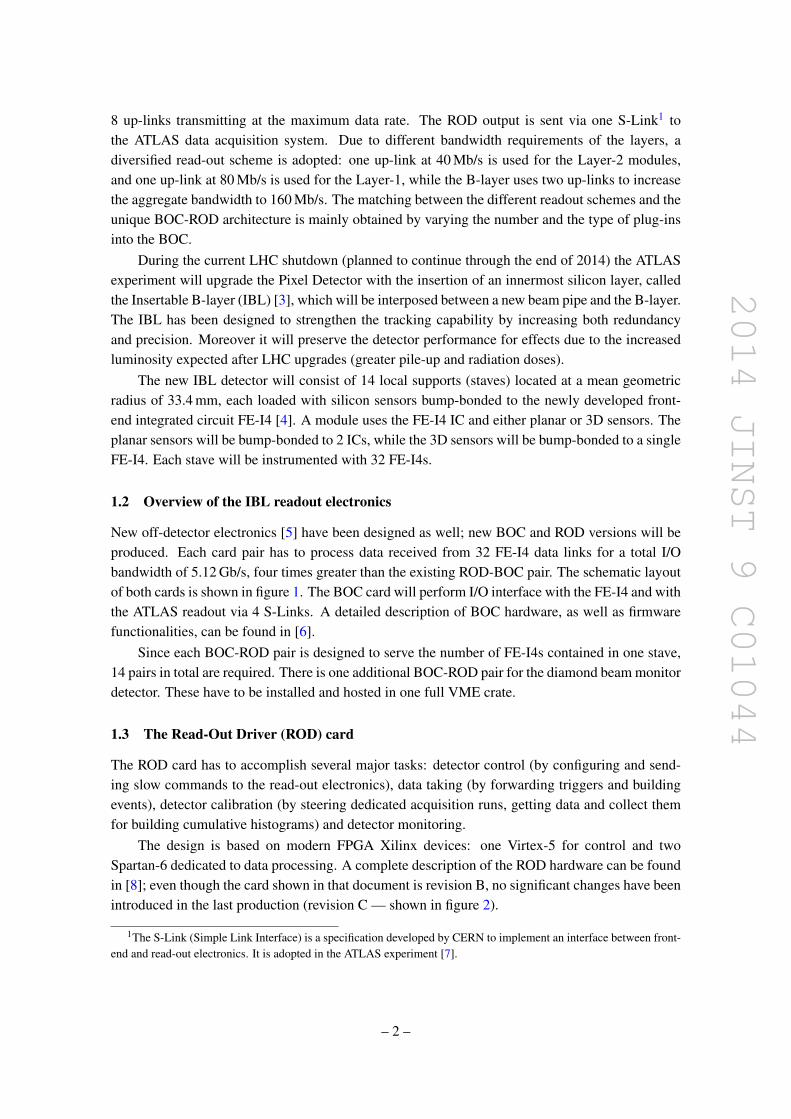
New off-detector electronics [5] have been designed as well new BOC and ROD versions will beproduced Each card pair has to process data received from 32 FE-I4 data links for a total IObandwidth of 512 Gbs four times greater than the existing ROD-BOC pair The schematic layoutof both cards is shown in figure 1 The BOC card will perform IO interface with the FE-I4 and withthe ATLAS readout via 4 S-Links A detailed description of BOC hardware as well as firmwarefunctionalities can be found in [6]
Since each BOC-ROD pair is designed to serve the number of FE-I4s contained in one stave14 pairs in total are required There is one additional BOC-ROD pair for the diamond beam monitordetector These have to be installed and hosted in one full VME crate
13 The Read-Out Driver (ROD) card
The ROD card has to accomplish several major tasks detector control (by configuring and send-ing slow commands to the read-out electronics) data taking (by forwarding triggers and buildingevents) detector calibration (by steering dedicated acquisition runs getting data and collect themfor building cumulative histograms) and detector monitoring
The design is based on modern FPGA Xilinx devices one Virtex-5 for control and twoSpartan-6 dedicated to data processing A complete description of the ROD hardware can be foundin [8] even though the card shown in that document is revision B no significant changes have beenintroduced in the last production (revision C mdash shown in figure 2)
1The S-Link (Simple Link Interface) is a specification developed by CERN to implement an interface between front-end and read-out electronics It is adopted in the ATLAS experiment [7]
ndash 2 ndash
2014 JINST 9 C01044
Figure 1 The layout of the IBL readout electronics
Figure 2 ROD revision C The Xilinx Virtex-5 is under the heat exchanger in the top right
2 The ROD production and commissioning
21 Prototyping pre-production and commissioning strategies
The first prototype batch (revision A) included 3 samples produced in September 2011 and wasmainly devoted to design and layout validation The second prototype batch of 5 cards (revision B)was delivered on February 2012 and included major bug fixes with respect to the previous versionSome samples of revision B were also distributed to collaborators to enlarge the community offirmware developers as well as to develop several test stands where different integration testscould be performed In February 2013 5 cards (revision C) were produced with minor changeswith respect to the previous iteration This batch is considered as a pre-production sample becauseit will be used to validate the overall board performance and design before starting to manufacturethe final boards They will also be used as spares for the final system Tests were performed inparallel in different laboratories with different set-ups Six test stands are available one at CERNtwo in Italy (Bologna and Genova) and three in Germany (Gottingen Mannheim and Wuppertal)
ndash 3 ndash
2014 JINST 9 C01044
22 ROD testing
As part of testing the prototype boards we have developed a comprehensive set of tests for boardbring-up and deployment The list of features that must be verified is the following
bull VME interface
bull FPGA firmware download both stand-alone and from VME
bull FPGA-embedded processors with software download from VME
bull TIM2 interface (VME module which connects with the ATLAS level-1 trigger system)
bull connectivity between FPGAs and memory components (DDR2 FLASH-based SynchronousStatic RAM)
bull three Gigabit Ethernet links
bull ROD bus (asynchronous bus to configure chips on both ROD and BOC)
bull buses to and from the BOC
Three specific tests will be discussed in the following as being particularly interesting In thefirst we will show how testing prototypes was decisive on finalizing some layout options in thesecond we will spotlight one typical case where complex approaches and custom solutions havebeen developed to face a quite difficult problem The last example will spotlight how integrationtests provided us reasonable confidence that the ROD required performance has been successfullyaccomplished
221 Test example 1 BOC to ROD transmission
The data received by the BOC from the FE-I4 after decoding is sent to the ROD via a 96-bit widebus with a single line signal rate of 80 Mbs The bus width and the signal rate have been dimen-sioned as a tradeoff between the bandwidth requirement between BOC and ROD (512 Gbs) andthe design modularity (12 bit is the width of the front-end data) The bus connects the Spartan-6FPGAs hosted on the different cards through the VME backplane connectors The communicationhas been implemented with the SSTL 3 standard [9] Transmission is double data rate synchro-nized with the 40 MHz clock common to both cards The bus has been designed to have minimalskew and to optimize the signal integrity in the PCB layout The decision whether to include busterminators external to the FPGA was postponed to a later stage terminations provide better signalintegrity but the increased routing congestion and the reduced space on the board have to be con-sidered Extensive tests have been performed with an ad-hoc firmware sending data continuouslyand measuring the bit error rate by varying the phase of the receiver clock The goal of this test wasto measure the width of the good sampling phase window A typical result for cards of revisions Aand B is shown in table 1
2The TIM (TTC Interface Module) is a VME board that distributes clock and trigger signals received from theTiming Trigger and Control (TTC) system to the cards hosted into the crate
ndash 4 ndash
2014 JINST 9 C01044
Table 1 Typical results for the BOC to ROD communication with revision B cards Different phases ofthe clock at the receiver side are tested Each value has been verified by sending data formatted as 12-bitfree-running counters continuously for 2 hours
Phase (degrees) Device Status Problems
0SP6A FAIL Multiple errors on every busSP6B FAIL Multiple errors on every bus
90SP6A FAIL Multiple errors on A busSP6B FAIL Multiple errors on B bus
180SP6A FAIL Sometimes read C8 instead of CC on A busSP6B OK
270SP6A OKSP6B OK
Table 2 Example of results for the BOC to ROD transmission with revision C cards The same patterns andduration as in table 1 have been used
Phase (degrees) Device Status Problems
0SP6A FAIL Multiple errors on every busSP6B FAIL Multiple errors on every bus
90SP6A FAIL One error in 2 hours of testSP6B OK
180SP6A OKSP6B OK
270SP6A OKSP6B OK
Due to unsatisfactory results we added compact package resistors onto the whole bus in re-vision C taking care to minimize changes on the current signal routing The result for one card isshown in table 2 The performance looked more satisfactory and we have seen good uniformitybetween cards
222 Test example 2 SRAM controller for calibration histograms
As it was previously mentioned (section 13) one of the tasks of the ROD card is to create his-tograms of the data for calibrating the detector Preliminary estimates show how scans whichrequired about 10 minutes with the existing electronics can be performed faster in the IBL RODSince the histograms are read-out via Gigabit Ethernet links acquisition runs with a comparableamount of data can be accomplished in about 10 seconds The most important speed limitation be-comes the maximum data rate of the Synchronous Static RAM (SSRAM) components Due to thecard design in order to manage histograms for all FE-I4s in parallel the selected SSRAM3 must beaccessed with a clock frequency of about 200 MHz Implementing such a 36-bit SSRAM controller
31Mx36 bit Synchronous Static RAM chips (Cypress CY7C1370D-250AXC-ND)
ndash 5 ndash
2014 JINST 9 C01044
running at 200 MHz in a Spartan-6 FPGA required adopting careful design techniques First theclock is forwarded to the SSRAM with matched PCB feedback paths Second the Spartan-6 PLLsare configured in ldquoZero delay bufferrdquo mode synchronizing both FPGA and SSRAM clocks Lastdistinct clock domains for the transmitter and receiver logic are implemented
Other issues have to be taken into account For IO pin driver properties carefully chosenvalues of both slew rate and current drive capability must be determined to get the fastest pad prop-agation delay without violating the maximum amount of simultaneous switching outputs allowedby the FPGAs
Finally effects due to bus contention have been evaluated This happens when two devicesare simultaneously driving a bi-directional line This is exacerbated by clock skew between thetransmitter and receiver elements Bus contention increases the power dissipation of the compo-nents Taking into account both the switching times of devices (from the datasheets) and relativeclock phases (from simulation) a temperature rise of less than 3C has been expected Even thoughit is a small effect we can reduce the effect further by grouping together several cycles with thesame access type (read or write) Tests have been performed at maximum achieved clock speed(200 MHz) measuring the increase of temperature (with a thermal camera) and showing that wesucceeded on limiting that effect
The interface with the SSRAM has been successfully tested at 200 MHz in stand-alone op-eration while a 140 MHz working version has been proven to work when integrated in the latestofficial release of the ROD firmware
223 Test example 3 integration with the FE-I4
Extensive tests have been performed connecting the FE-I4 to a BOC-ROD pair Their major aimis to validate the resources implemented on both cards (eg the amount of memory available in thechosen components) showing that hardware specifications have been met Moreover integrationtests have been performed to drive the firmware design and development with real use cases
The official version of the firmware is shown in figure 3 The design is highly modular Fourgroups of 8 FE-I4 (4 modules) are processed independently on the BOC and then transmitted to acollector block in the ROD (called the ldquogathererrdquo) Then an event builder (EFB) multiplexes databoth to an S-Link interface and to a dedicated component (called histogrammer) that accumulatesevents and fills summary histograms (occupancy time over threshold ToT per pixel ToT2 perpixel) The histogrammer stores temporary data in the SSRAMs At the end of the acquisition thehistograms are read by an embedded microcontroller (a Xilinx MicroBlaze IP core) via DMA andloaded into the DDR2 They are then sent to an external PC farm through Gigabit Ethernet linkThe PowerPC microcontroller embedded in the ROD Virtex-5 controls all the subsystems and actsas an interface to the software application that executes this test At the present time the test standis composed by two FE-I4s connected to the same datapath (see green lines in figure 3)
The results are satisfactory the basic implemented functionalities are adequate to successfullyperform data acquisition and calibration scans with FPGA resource utilization of less than 20This allows us to be confident that a more realistic version (with busy logic timeouts completeerror handling etc) will fit on the chip Moreover the whole mechanism of histogram filling andacquisition has been evaluated showing how all requirements will be met even when it will operate
ndash 6 ndash
2014 JINST 9 C01044
Figure 3 Schematic layout of the BOC-ROD firmware Only one Spartan-6 for both BOC and ROD areshown the others have an identical design The green lines represent the data paths currently under test Theorange lines indicate the ROD bus for configuring and monitoring the processing blocks
with the full set of FE-I4s connected Thus the choice of the specific components installed in theROD has been confirmed and the overall board design validated
23 ROD production plans and validation procedures
At the present time the ROD design has been successfully validated and readied for production forIBL The same firm that delivered all prototype batches will do the PCB manufacturing and assem-bly After production preliminary tests (similar to those of revision B and C) will be delegated tothe same company electrical examination after components supply and Xray inspection for largeBGA-packaged devices
We also defined a list of minimal procedures to validate the ROD cards after production
bull firmware-software upload from VME JTAG and Gigabit Ethernet ports
bull ROD to BOC (and BOC to ROD) dataflow over all IO lines
bull RW tests for Virtex-5 and Spartan-6 external memory modules
bull dataflow tests on the 3 Ethernet ports
bull TIM card connectivity test
ndash 7 ndash
2014 JINST 9 C01044
Figure 4 Synchronization errors in runs acquired last year The y-axis is the maximum number of modulesthat showed synchronization errors at a given event The ROD verifies the synchronization of the data linkby checking both encoded data format and the event counter The synchronization during data taking isautomatically restored by issuing an event counter reset every few seconds As an example a ldquoSynchroniza-tion ErrorEventrdquo of 50 means that an inefficiency of 50 out of 1700 (the number of modules in Layer 2)occurred for few seconds The excess shown by Layer 2 links with respect to the others are probably due tobandwidth limitation
These tests will be performed before the board installation on the experiment The firm hasbeen hired to produce 15 cards identical to revision C at the end of August 2013 fulfilling theproduction requirements for IBL Delivery is expected by mid October
3 Review on upgrade for read-out electronics of Layer 1 and Layer 2
With the restart of LHC (2014) we are expecting a higher luminosity which will increase evenmore in subsequent years As a consequence we foresee that the Pixel readout link of the actualdetector will suffer from bandwidth limitations The link bandwidth is proportional to the productof occupancy and trigger rate of the front-end devices The first is a function of the luminosity andcan be extrapolated using the experience gained from previous years of data acquisition Prelimi-nary measurements show that even with an average number of expected pile-up events 〈micro〉 asymp 50(a reasonable estimation for luminosity energy and bunch spacing expected by 2015) and triggerrate of 100 kHz the estimated average link occupancy for Layer 2 is about 90
With greater pile-up (when luminosity will be greater than 2 middot 1034 cmminus2 sminus1) even Layer 1will get into trouble Moreover in the last run Layer 2 already showed several synchronizationerrors probably due to bandwidth limitation even though the average link occupancy was about50 (figure 4)
The actions that could be taken are different in Layer 1 and Layer 2 Layer 2 is read-out withone link per module at 40 Mbs Increasing the bandwidth to 80 Mbs is a viable solution it wouldrequire producing more BOC opto-electrical plug-ins as well as more BOC-ROD pairs (to support
ndash 8 ndash
2014 JINST 9 C01044
double the bandwidth) and rearranging the link cabling Since IBL off-detector electronics alreadymanage BOC-ROD transmissions at 80 Mbs (section 4) it would be straightforward to adopt IBLcards Only two minor modifications would be needed a new firmware and new custom RX opto-electrical BOC plug-ins No change in connectivity and fiber routing is foreseen
Layer 1 is already able to manage read-out at 80 Mbs therefore installing a second link permodule can increase the bandwidth As in the previous case the adoption of IBL cards wouldrequire both new firmware and BOC plug-ins with minor modifications of the connections
The adoption of IBL ROD-BOC cards would bring also more benefits because of the stan-dardized design it will provide a uniform board for most of the Pixel read-out system and providecommon spares for all sub-detectors No modifications will be needed to the ROD design so pro-duction can start immediately and the board will be ready by the LHC restart 26 ROD will beneeded for Layer 2 and 38 for Layer 1 No official decisions on board deployment have been takenyet but discussions are ongoing
References
[1] ATLAS collaboration The ATLAS experiment at the CERN Large Hadron Collider2008 JINST 3 S08003
[2] G Aad et al ATLAS pixel detector electronics and sensors 2008 JINST 3 P07007
[3] ATLAS collaboration ATLAS Insertable B-Layer technical design report CERN-LHCC-2010-013
[4] ATLAS IBL collaboration Prototype ATLAS IBL modules using the FE-I4A front-end readout chip2012 JINST 7 P11010
[5] J Dopke et al The IBL readout system 2011 JINST 6 C01006
[6] M Wensing Testing and firmware development for the ATLAS IBL BOC prototype2012 JINST 7 C12027
[7] HC van der Bij et al S-LINK a prototype of the ATLAS read-out link in Proceedings of the FourthWorkshop on Electronics for LHC Experiments Rome Italy 21ndash25 Sep 1998
[8] G Balbi et al Implementation and tests of FPGA-embedded PowerPC in the control system of theATLAS IBL ROD card 2013 JINST 8 C01012
[9] JEDEC Solid State Technology Association Stub-series terminated logic for 33 volts (SSTL 3)JESD8-8 (1996)
ndash 9 ndash
2014 JINST 9 C01044
PUBLISHED BY IOP PUBLISHING FOR SISSA MEDIALAB
RECEIVED November 14 2013ACCEPTED December 17 2013
PUBLISHED January 23 2014
TOPICAL WORKSHOP ON ELECTRONICS FOR PARTICLE PHYSICS 201323ndash27 SEPTEMBER 2013PERUGIA ITALY
ldquoThe Read-Out Driverrdquo ROD card for the InsertableB-layer (IBL) detector of the ATLAS experimentcommissioning and upgrade studies for the PixelLayers 1 and 2
G Balbia M Bindia SP Chenb D Falchieric T Flickd A Gabriellic S Hauckb
SC Hsub M Kretze A Kugele L Lamac P Morettini f R Travaglinia1
and M Wensingd
aINFN mdash Sezione di Bolognavle B Pichat 62 Bologna Italy
bUniversity of Washington3910 15th Ave NE Seattle WA USA
cUniversity of Bologna amp INFN Bolognavle B Pichat 62 Bologna Italy
dFachbereich C Physik WuppertalGauss-str 20 Wuppertal Germany
eUniversity of HeidelbergZITIB6 26 Mannheim Germany
f INFN mdash Sezione di Genovavia Dodecaneso 33 Genova Italy
E-mail RiccardoTravagliniboinfnit
ABSTRACT The upgrade of the ATLAS experiment at LHC foresees the insertion of an innermostsilicon layer called the Insertable B-layer (IBL) The IBL read-out system will be equipped withnew electronics The Readout-Driver card (ROD) is a VME board devoted to data processingconfiguration and control A pre-production batch has been delivered for testing with instrumentedslices of the overall acquisition chain aiming to finalize strategies for system commissioning Inthis paper system setups and results will be described as well as preliminary studies on changesneeded to adopt the ROD for the ATLAS Pixel Layers 1 and 2
KEYWORDS Data acquisition circuits Detector control systems (detector and experiment moni-toring and slow-control systems architecture hardware algorithms databases) Digital electroniccircuits
1Corresponding author
ccopy CERN 2014 published under the terms of the Creative Commons Attribution 30License by IOP Publishing Ltd and Sissa Medialab srl Any further distribution of this
work must maintain attribution to the author(s) and the published articlersquos title journal citation and DOIdoi1010881748-0221901C01044
2014 JINST 9 C01044
Contents
1 Introduction 111 The ATLAS Pixel detector and the Insertable Barrel Layer (IBL) for the upgrade
phase-0 112 Overview of the IBL readout electronics 213 The Read-Out Driver (ROD) card 2
2 The ROD production and commissioning 321 Prototyping pre-production and commissioning strategies 322 ROD testing 4
221 Test example 1 BOC to ROD transmission 4222 Test example 2 SRAM controller for calibration histograms 5223 Test example 3 integration with the FE-I4 6
23 ROD production plans and validation procedures 7
3 Review on upgrade for read-out electronics of Layer 1 and Layer 2 8
1 Introduction
11 The ATLAS Pixel detector and the Insertable Barrel Layer (IBL) for the upgradephase-0
The ATLAS experiment [1] is a general-purpose detector for the LHC at CERN It consists ofseveral sub-detectors designed with different technologies The Pixel Detector [2] is the innermostone installed just around the beam interaction point and devoted to tracking and vertex reconstruc-tion The system is arranged in three concentric cylinders (the barrel) and three disks at each barrelextremity (the end-caps) The mean radius of the barrel layer closest to the beam pipe (B-layer) is5 cm The basic building block of the active part of the Pixel Detector is a module that is composedof silicon sensors and front-end electronics Each module is equipped with 16 front-end ASICscalled FE-I3 which are read out by a Module Control Chip (MCC) Each MCC is connected withthe off-detector electronics via two links the down-link is used to transmit clock trigger com-mands and configuration data to the front-end while one or two named up-links are used for eventreadout Each up-link can be configured to transmit at either 40 Mbs or 80 Mbs data rates
The off-detector basic readout unit is composed of two 9U-VME cards the Back-of-Crate(BOC) and the Read-Out Driver (ROD) implementing an optical IO interface and data processingrespectively They are paired back-to-back in the same VME slot Electrical-to-optical conversionof link transmission occurs in custom opto-boards on the detector side and in the optical-receiver(RX) and optical-transmitter (TX) plug-ins in the BOC Readout data is then transmitted to thepaired ROD (via the backplane) that processes the data and performs event building Each BOC-ROD pair can sustain an aggregate output bandwidth of up to 160 MBs which correspond to
ndash 1 ndash
2014 JINST 9 C01044
8 up-links transmitting at the maximum data rate The ROD output is sent via one S-Link1 tothe ATLAS data acquisition system Due to different bandwidth requirements of the layers adiversified read-out scheme is adopted one up-link at 40 Mbs is used for the Layer-2 modulesand one up-link at 80 Mbs is used for the Layer-1 while the B-layer uses two up-links to increasethe aggregate bandwidth to 160 Mbs The matching between the different readout schemes and theunique BOC-ROD architecture is mainly obtained by varying the number and the type of plug-insinto the BOC
During the current LHC shutdown (planned to continue through the end of 2014) the ATLASexperiment will upgrade the Pixel Detector with the insertion of an innermost silicon layer calledthe Insertable B-layer (IBL) [3] which will be interposed between a new beam pipe and the B-layerThe IBL has been designed to strengthen the tracking capability by increasing both redundancyand precision Moreover it will preserve the detector performance for effects due to the increasedluminosity expected after LHC upgrades (greater pile-up and radiation doses)
The new IBL detector will consist of 14 local supports (staves) located at a mean geometricradius of 334 mm each loaded with silicon sensors bump-bonded to the newly developed front-end integrated circuit FE-I4 [4] A module uses the FE-I4 IC and either planar or 3D sensors Theplanar sensors will be bump-bonded to 2 ICs while the 3D sensors will be bump-bonded to a singleFE-I4 Each stave will be instrumented with 32 FE-I4s
12 Overview of the IBL readout electronics
New off-detector electronics [5] have been designed as well new BOC and ROD versions will beproduced Each card pair has to process data received from 32 FE-I4 data links for a total IObandwidth of 512 Gbs four times greater than the existing ROD-BOC pair The schematic layoutof both cards is shown in figure 1 The BOC card will perform IO interface with the FE-I4 and withthe ATLAS readout via 4 S-Links A detailed description of BOC hardware as well as firmwarefunctionalities can be found in [6]
Since each BOC-ROD pair is designed to serve the number of FE-I4s contained in one stave14 pairs in total are required There is one additional BOC-ROD pair for the diamond beam monitordetector These have to be installed and hosted in one full VME crate
13 The Read-Out Driver (ROD) card
The ROD card has to accomplish several major tasks detector control (by configuring and send-ing slow commands to the read-out electronics) data taking (by forwarding triggers and buildingevents) detector calibration (by steering dedicated acquisition runs getting data and collect themfor building cumulative histograms) and detector monitoring
The design is based on modern FPGA Xilinx devices one Virtex-5 for control and twoSpartan-6 dedicated to data processing A complete description of the ROD hardware can be foundin [8] even though the card shown in that document is revision B no significant changes have beenintroduced in the last production (revision C mdash shown in figure 2)
1The S-Link (Simple Link Interface) is a specification developed by CERN to implement an interface between front-end and read-out electronics It is adopted in the ATLAS experiment [7]
ndash 2 ndash
2014 JINST 9 C01044
Figure 1 The layout of the IBL readout electronics
Figure 2 ROD revision C The Xilinx Virtex-5 is under the heat exchanger in the top right
2 The ROD production and commissioning
21 Prototyping pre-production and commissioning strategies
The first prototype batch (revision A) included 3 samples produced in September 2011 and wasmainly devoted to design and layout validation The second prototype batch of 5 cards (revision B)was delivered on February 2012 and included major bug fixes with respect to the previous versionSome samples of revision B were also distributed to collaborators to enlarge the community offirmware developers as well as to develop several test stands where different integration testscould be performed In February 2013 5 cards (revision C) were produced with minor changeswith respect to the previous iteration This batch is considered as a pre-production sample becauseit will be used to validate the overall board performance and design before starting to manufacturethe final boards They will also be used as spares for the final system Tests were performed inparallel in different laboratories with different set-ups Six test stands are available one at CERNtwo in Italy (Bologna and Genova) and three in Germany (Gottingen Mannheim and Wuppertal)
ndash 3 ndash
2014 JINST 9 C01044
22 ROD testing
As part of testing the prototype boards we have developed a comprehensive set of tests for boardbring-up and deployment The list of features that must be verified is the following
bull VME interface
bull FPGA firmware download both stand-alone and from VME
bull FPGA-embedded processors with software download from VME
bull TIM2 interface (VME module which connects with the ATLAS level-1 trigger system)
bull connectivity between FPGAs and memory components (DDR2 FLASH-based SynchronousStatic RAM)
bull three Gigabit Ethernet links
bull ROD bus (asynchronous bus to configure chips on both ROD and BOC)
bull buses to and from the BOC
Three specific tests will be discussed in the following as being particularly interesting In thefirst we will show how testing prototypes was decisive on finalizing some layout options in thesecond we will spotlight one typical case where complex approaches and custom solutions havebeen developed to face a quite difficult problem The last example will spotlight how integrationtests provided us reasonable confidence that the ROD required performance has been successfullyaccomplished
221 Test example 1 BOC to ROD transmission
The data received by the BOC from the FE-I4 after decoding is sent to the ROD via a 96-bit widebus with a single line signal rate of 80 Mbs The bus width and the signal rate have been dimen-sioned as a tradeoff between the bandwidth requirement between BOC and ROD (512 Gbs) andthe design modularity (12 bit is the width of the front-end data) The bus connects the Spartan-6FPGAs hosted on the different cards through the VME backplane connectors The communicationhas been implemented with the SSTL 3 standard [9] Transmission is double data rate synchro-nized with the 40 MHz clock common to both cards The bus has been designed to have minimalskew and to optimize the signal integrity in the PCB layout The decision whether to include busterminators external to the FPGA was postponed to a later stage terminations provide better signalintegrity but the increased routing congestion and the reduced space on the board have to be con-sidered Extensive tests have been performed with an ad-hoc firmware sending data continuouslyand measuring the bit error rate by varying the phase of the receiver clock The goal of this test wasto measure the width of the good sampling phase window A typical result for cards of revisions Aand B is shown in table 1
2The TIM (TTC Interface Module) is a VME board that distributes clock and trigger signals received from theTiming Trigger and Control (TTC) system to the cards hosted into the crate
ndash 4 ndash
2014 JINST 9 C01044
Table 1 Typical results for the BOC to ROD communication with revision B cards Different phases ofthe clock at the receiver side are tested Each value has been verified by sending data formatted as 12-bitfree-running counters continuously for 2 hours
Phase (degrees) Device Status Problems
0SP6A FAIL Multiple errors on every busSP6B FAIL Multiple errors on every bus
90SP6A FAIL Multiple errors on A busSP6B FAIL Multiple errors on B bus
180SP6A FAIL Sometimes read C8 instead of CC on A busSP6B OK
270SP6A OKSP6B OK
Table 2 Example of results for the BOC to ROD transmission with revision C cards The same patterns andduration as in table 1 have been used
Phase (degrees) Device Status Problems
0SP6A FAIL Multiple errors on every busSP6B FAIL Multiple errors on every bus
90SP6A FAIL One error in 2 hours of testSP6B OK
180SP6A OKSP6B OK
270SP6A OKSP6B OK
Due to unsatisfactory results we added compact package resistors onto the whole bus in re-vision C taking care to minimize changes on the current signal routing The result for one card isshown in table 2 The performance looked more satisfactory and we have seen good uniformitybetween cards
222 Test example 2 SRAM controller for calibration histograms
As it was previously mentioned (section 13) one of the tasks of the ROD card is to create his-tograms of the data for calibrating the detector Preliminary estimates show how scans whichrequired about 10 minutes with the existing electronics can be performed faster in the IBL RODSince the histograms are read-out via Gigabit Ethernet links acquisition runs with a comparableamount of data can be accomplished in about 10 seconds The most important speed limitation be-comes the maximum data rate of the Synchronous Static RAM (SSRAM) components Due to thecard design in order to manage histograms for all FE-I4s in parallel the selected SSRAM3 must beaccessed with a clock frequency of about 200 MHz Implementing such a 36-bit SSRAM controller
31Mx36 bit Synchronous Static RAM chips (Cypress CY7C1370D-250AXC-ND)
ndash 5 ndash
2014 JINST 9 C01044
running at 200 MHz in a Spartan-6 FPGA required adopting careful design techniques First theclock is forwarded to the SSRAM with matched PCB feedback paths Second the Spartan-6 PLLsare configured in ldquoZero delay bufferrdquo mode synchronizing both FPGA and SSRAM clocks Lastdistinct clock domains for the transmitter and receiver logic are implemented
Other issues have to be taken into account For IO pin driver properties carefully chosenvalues of both slew rate and current drive capability must be determined to get the fastest pad prop-agation delay without violating the maximum amount of simultaneous switching outputs allowedby the FPGAs
Finally effects due to bus contention have been evaluated This happens when two devicesare simultaneously driving a bi-directional line This is exacerbated by clock skew between thetransmitter and receiver elements Bus contention increases the power dissipation of the compo-nents Taking into account both the switching times of devices (from the datasheets) and relativeclock phases (from simulation) a temperature rise of less than 3C has been expected Even thoughit is a small effect we can reduce the effect further by grouping together several cycles with thesame access type (read or write) Tests have been performed at maximum achieved clock speed(200 MHz) measuring the increase of temperature (with a thermal camera) and showing that wesucceeded on limiting that effect
The interface with the SSRAM has been successfully tested at 200 MHz in stand-alone op-eration while a 140 MHz working version has been proven to work when integrated in the latestofficial release of the ROD firmware
223 Test example 3 integration with the FE-I4
Extensive tests have been performed connecting the FE-I4 to a BOC-ROD pair Their major aimis to validate the resources implemented on both cards (eg the amount of memory available in thechosen components) showing that hardware specifications have been met Moreover integrationtests have been performed to drive the firmware design and development with real use cases
The official version of the firmware is shown in figure 3 The design is highly modular Fourgroups of 8 FE-I4 (4 modules) are processed independently on the BOC and then transmitted to acollector block in the ROD (called the ldquogathererrdquo) Then an event builder (EFB) multiplexes databoth to an S-Link interface and to a dedicated component (called histogrammer) that accumulatesevents and fills summary histograms (occupancy time over threshold ToT per pixel ToT2 perpixel) The histogrammer stores temporary data in the SSRAMs At the end of the acquisition thehistograms are read by an embedded microcontroller (a Xilinx MicroBlaze IP core) via DMA andloaded into the DDR2 They are then sent to an external PC farm through Gigabit Ethernet linkThe PowerPC microcontroller embedded in the ROD Virtex-5 controls all the subsystems and actsas an interface to the software application that executes this test At the present time the test standis composed by two FE-I4s connected to the same datapath (see green lines in figure 3)
The results are satisfactory the basic implemented functionalities are adequate to successfullyperform data acquisition and calibration scans with FPGA resource utilization of less than 20This allows us to be confident that a more realistic version (with busy logic timeouts completeerror handling etc) will fit on the chip Moreover the whole mechanism of histogram filling andacquisition has been evaluated showing how all requirements will be met even when it will operate
ndash 6 ndash
2014 JINST 9 C01044
Figure 3 Schematic layout of the BOC-ROD firmware Only one Spartan-6 for both BOC and ROD areshown the others have an identical design The green lines represent the data paths currently under test Theorange lines indicate the ROD bus for configuring and monitoring the processing blocks
with the full set of FE-I4s connected Thus the choice of the specific components installed in theROD has been confirmed and the overall board design validated
23 ROD production plans and validation procedures
At the present time the ROD design has been successfully validated and readied for production forIBL The same firm that delivered all prototype batches will do the PCB manufacturing and assem-bly After production preliminary tests (similar to those of revision B and C) will be delegated tothe same company electrical examination after components supply and Xray inspection for largeBGA-packaged devices
We also defined a list of minimal procedures to validate the ROD cards after production
bull firmware-software upload from VME JTAG and Gigabit Ethernet ports
bull ROD to BOC (and BOC to ROD) dataflow over all IO lines
bull RW tests for Virtex-5 and Spartan-6 external memory modules
bull dataflow tests on the 3 Ethernet ports
bull TIM card connectivity test
ndash 7 ndash
2014 JINST 9 C01044
Figure 4 Synchronization errors in runs acquired last year The y-axis is the maximum number of modulesthat showed synchronization errors at a given event The ROD verifies the synchronization of the data linkby checking both encoded data format and the event counter The synchronization during data taking isautomatically restored by issuing an event counter reset every few seconds As an example a ldquoSynchroniza-tion ErrorEventrdquo of 50 means that an inefficiency of 50 out of 1700 (the number of modules in Layer 2)occurred for few seconds The excess shown by Layer 2 links with respect to the others are probably due tobandwidth limitation
These tests will be performed before the board installation on the experiment The firm hasbeen hired to produce 15 cards identical to revision C at the end of August 2013 fulfilling theproduction requirements for IBL Delivery is expected by mid October
3 Review on upgrade for read-out electronics of Layer 1 and Layer 2
With the restart of LHC (2014) we are expecting a higher luminosity which will increase evenmore in subsequent years As a consequence we foresee that the Pixel readout link of the actualdetector will suffer from bandwidth limitations The link bandwidth is proportional to the productof occupancy and trigger rate of the front-end devices The first is a function of the luminosity andcan be extrapolated using the experience gained from previous years of data acquisition Prelimi-nary measurements show that even with an average number of expected pile-up events 〈micro〉 asymp 50(a reasonable estimation for luminosity energy and bunch spacing expected by 2015) and triggerrate of 100 kHz the estimated average link occupancy for Layer 2 is about 90
With greater pile-up (when luminosity will be greater than 2 middot 1034 cmminus2 sminus1) even Layer 1will get into trouble Moreover in the last run Layer 2 already showed several synchronizationerrors probably due to bandwidth limitation even though the average link occupancy was about50 (figure 4)
The actions that could be taken are different in Layer 1 and Layer 2 Layer 2 is read-out withone link per module at 40 Mbs Increasing the bandwidth to 80 Mbs is a viable solution it wouldrequire producing more BOC opto-electrical plug-ins as well as more BOC-ROD pairs (to support
ndash 8 ndash
2014 JINST 9 C01044
double the bandwidth) and rearranging the link cabling Since IBL off-detector electronics alreadymanage BOC-ROD transmissions at 80 Mbs (section 4) it would be straightforward to adopt IBLcards Only two minor modifications would be needed a new firmware and new custom RX opto-electrical BOC plug-ins No change in connectivity and fiber routing is foreseen
Layer 1 is already able to manage read-out at 80 Mbs therefore installing a second link permodule can increase the bandwidth As in the previous case the adoption of IBL cards wouldrequire both new firmware and BOC plug-ins with minor modifications of the connections
The adoption of IBL ROD-BOC cards would bring also more benefits because of the stan-dardized design it will provide a uniform board for most of the Pixel read-out system and providecommon spares for all sub-detectors No modifications will be needed to the ROD design so pro-duction can start immediately and the board will be ready by the LHC restart 26 ROD will beneeded for Layer 2 and 38 for Layer 1 No official decisions on board deployment have been takenyet but discussions are ongoing
References
[1] ATLAS collaboration The ATLAS experiment at the CERN Large Hadron Collider2008 JINST 3 S08003
[2] G Aad et al ATLAS pixel detector electronics and sensors 2008 JINST 3 P07007
[3] ATLAS collaboration ATLAS Insertable B-Layer technical design report CERN-LHCC-2010-013
[4] ATLAS IBL collaboration Prototype ATLAS IBL modules using the FE-I4A front-end readout chip2012 JINST 7 P11010
[5] J Dopke et al The IBL readout system 2011 JINST 6 C01006
[6] M Wensing Testing and firmware development for the ATLAS IBL BOC prototype2012 JINST 7 C12027
[7] HC van der Bij et al S-LINK a prototype of the ATLAS read-out link in Proceedings of the FourthWorkshop on Electronics for LHC Experiments Rome Italy 21ndash25 Sep 1998
[8] G Balbi et al Implementation and tests of FPGA-embedded PowerPC in the control system of theATLAS IBL ROD card 2013 JINST 8 C01012
[9] JEDEC Solid State Technology Association Stub-series terminated logic for 33 volts (SSTL 3)JESD8-8 (1996)
ndash 9 ndash

2014 JINST 9 C01044
Contents
1 Introduction 111 The ATLAS Pixel detector and the Insertable Barrel Layer (IBL) for the upgrade
phase-0 112 Overview of the IBL readout electronics 213 The Read-Out Driver (ROD) card 2
2 The ROD production and commissioning 321 Prototyping pre-production and commissioning strategies 322 ROD testing 4
221 Test example 1 BOC to ROD transmission 4222 Test example 2 SRAM controller for calibration histograms 5223 Test example 3 integration with the FE-I4 6
23 ROD production plans and validation procedures 7
3 Review on upgrade for read-out electronics of Layer 1 and Layer 2 8
1 Introduction
11 The ATLAS Pixel detector and the Insertable Barrel Layer (IBL) for the upgradephase-0
The ATLAS experiment [1] is a general-purpose detector for the LHC at CERN It consists ofseveral sub-detectors designed with different technologies The Pixel Detector [2] is the innermostone installed just around the beam interaction point and devoted to tracking and vertex reconstruc-tion The system is arranged in three concentric cylinders (the barrel) and three disks at each barrelextremity (the end-caps) The mean radius of the barrel layer closest to the beam pipe (B-layer) is5 cm The basic building block of the active part of the Pixel Detector is a module that is composedof silicon sensors and front-end electronics Each module is equipped with 16 front-end ASICscalled FE-I3 which are read out by a Module Control Chip (MCC) Each MCC is connected withthe off-detector electronics via two links the down-link is used to transmit clock trigger com-mands and configuration data to the front-end while one or two named up-links are used for eventreadout Each up-link can be configured to transmit at either 40 Mbs or 80 Mbs data rates
The off-detector basic readout unit is composed of two 9U-VME cards the Back-of-Crate(BOC) and the Read-Out Driver (ROD) implementing an optical IO interface and data processingrespectively They are paired back-to-back in the same VME slot Electrical-to-optical conversionof link transmission occurs in custom opto-boards on the detector side and in the optical-receiver(RX) and optical-transmitter (TX) plug-ins in the BOC Readout data is then transmitted to thepaired ROD (via the backplane) that processes the data and performs event building Each BOC-ROD pair can sustain an aggregate output bandwidth of up to 160 MBs which correspond to
ndash 1 ndash
2014 JINST 9 C01044
8 up-links transmitting at the maximum data rate The ROD output is sent via one S-Link1 tothe ATLAS data acquisition system Due to different bandwidth requirements of the layers adiversified read-out scheme is adopted one up-link at 40 Mbs is used for the Layer-2 modulesand one up-link at 80 Mbs is used for the Layer-1 while the B-layer uses two up-links to increasethe aggregate bandwidth to 160 Mbs The matching between the different readout schemes and theunique BOC-ROD architecture is mainly obtained by varying the number and the type of plug-insinto the BOC
During the current LHC shutdown (planned to continue through the end of 2014) the ATLASexperiment will upgrade the Pixel Detector with the insertion of an innermost silicon layer calledthe Insertable B-layer (IBL) [3] which will be interposed between a new beam pipe and the B-layerThe IBL has been designed to strengthen the tracking capability by increasing both redundancyand precision Moreover it will preserve the detector performance for effects due to the increasedluminosity expected after LHC upgrades (greater pile-up and radiation doses)
The new IBL detector will consist of 14 local supports (staves) located at a mean geometricradius of 334 mm each loaded with silicon sensors bump-bonded to the newly developed front-end integrated circuit FE-I4 [4] A module uses the FE-I4 IC and either planar or 3D sensors Theplanar sensors will be bump-bonded to 2 ICs while the 3D sensors will be bump-bonded to a singleFE-I4 Each stave will be instrumented with 32 FE-I4s
12 Overview of the IBL readout electronics
New off-detector electronics [5] have been designed as well new BOC and ROD versions will beproduced Each card pair has to process data received from 32 FE-I4 data links for a total IObandwidth of 512 Gbs four times greater than the existing ROD-BOC pair The schematic layoutof both cards is shown in figure 1 The BOC card will perform IO interface with the FE-I4 and withthe ATLAS readout via 4 S-Links A detailed description of BOC hardware as well as firmwarefunctionalities can be found in [6]
Since each BOC-ROD pair is designed to serve the number of FE-I4s contained in one stave14 pairs in total are required There is one additional BOC-ROD pair for the diamond beam monitordetector These have to be installed and hosted in one full VME crate
13 The Read-Out Driver (ROD) card
The ROD card has to accomplish several major tasks detector control (by configuring and send-ing slow commands to the read-out electronics) data taking (by forwarding triggers and buildingevents) detector calibration (by steering dedicated acquisition runs getting data and collect themfor building cumulative histograms) and detector monitoring
The design is based on modern FPGA Xilinx devices one Virtex-5 for control and twoSpartan-6 dedicated to data processing A complete description of the ROD hardware can be foundin [8] even though the card shown in that document is revision B no significant changes have beenintroduced in the last production (revision C mdash shown in figure 2)
1The S-Link (Simple Link Interface) is a specification developed by CERN to implement an interface between front-end and read-out electronics It is adopted in the ATLAS experiment [7]
ndash 2 ndash
2014 JINST 9 C01044
Figure 1 The layout of the IBL readout electronics
Figure 2 ROD revision C The Xilinx Virtex-5 is under the heat exchanger in the top right
2 The ROD production and commissioning
21 Prototyping pre-production and commissioning strategies
The first prototype batch (revision A) included 3 samples produced in September 2011 and wasmainly devoted to design and layout validation The second prototype batch of 5 cards (revision B)was delivered on February 2012 and included major bug fixes with respect to the previous versionSome samples of revision B were also distributed to collaborators to enlarge the community offirmware developers as well as to develop several test stands where different integration testscould be performed In February 2013 5 cards (revision C) were produced with minor changeswith respect to the previous iteration This batch is considered as a pre-production sample becauseit will be used to validate the overall board performance and design before starting to manufacturethe final boards They will also be used as spares for the final system Tests were performed inparallel in different laboratories with different set-ups Six test stands are available one at CERNtwo in Italy (Bologna and Genova) and three in Germany (Gottingen Mannheim and Wuppertal)
ndash 3 ndash
2014 JINST 9 C01044
22 ROD testing
As part of testing the prototype boards we have developed a comprehensive set of tests for boardbring-up and deployment The list of features that must be verified is the following
bull VME interface
bull FPGA firmware download both stand-alone and from VME
bull FPGA-embedded processors with software download from VME
bull TIM2 interface (VME module which connects with the ATLAS level-1 trigger system)
bull connectivity between FPGAs and memory components (DDR2 FLASH-based SynchronousStatic RAM)
bull three Gigabit Ethernet links
bull ROD bus (asynchronous bus to configure chips on both ROD and BOC)
bull buses to and from the BOC
Three specific tests will be discussed in the following as being particularly interesting In thefirst we will show how testing prototypes was decisive on finalizing some layout options in thesecond we will spotlight one typical case where complex approaches and custom solutions havebeen developed to face a quite difficult problem The last example will spotlight how integrationtests provided us reasonable confidence that the ROD required performance has been successfullyaccomplished
221 Test example 1 BOC to ROD transmission
The data received by the BOC from the FE-I4 after decoding is sent to the ROD via a 96-bit widebus with a single line signal rate of 80 Mbs The bus width and the signal rate have been dimen-sioned as a tradeoff between the bandwidth requirement between BOC and ROD (512 Gbs) andthe design modularity (12 bit is the width of the front-end data) The bus connects the Spartan-6FPGAs hosted on the different cards through the VME backplane connectors The communicationhas been implemented with the SSTL 3 standard [9] Transmission is double data rate synchro-nized with the 40 MHz clock common to both cards The bus has been designed to have minimalskew and to optimize the signal integrity in the PCB layout The decision whether to include busterminators external to the FPGA was postponed to a later stage terminations provide better signalintegrity but the increased routing congestion and the reduced space on the board have to be con-sidered Extensive tests have been performed with an ad-hoc firmware sending data continuouslyand measuring the bit error rate by varying the phase of the receiver clock The goal of this test wasto measure the width of the good sampling phase window A typical result for cards of revisions Aand B is shown in table 1
2The TIM (TTC Interface Module) is a VME board that distributes clock and trigger signals received from theTiming Trigger and Control (TTC) system to the cards hosted into the crate
ndash 4 ndash
2014 JINST 9 C01044
Table 1 Typical results for the BOC to ROD communication with revision B cards Different phases ofthe clock at the receiver side are tested Each value has been verified by sending data formatted as 12-bitfree-running counters continuously for 2 hours
Phase (degrees) Device Status Problems
0SP6A FAIL Multiple errors on every busSP6B FAIL Multiple errors on every bus
90SP6A FAIL Multiple errors on A busSP6B FAIL Multiple errors on B bus
180SP6A FAIL Sometimes read C8 instead of CC on A busSP6B OK
270SP6A OKSP6B OK
Table 2 Example of results for the BOC to ROD transmission with revision C cards The same patterns andduration as in table 1 have been used
Phase (degrees) Device Status Problems
0SP6A FAIL Multiple errors on every busSP6B FAIL Multiple errors on every bus
90SP6A FAIL One error in 2 hours of testSP6B OK
180SP6A OKSP6B OK
270SP6A OKSP6B OK
Due to unsatisfactory results we added compact package resistors onto the whole bus in re-vision C taking care to minimize changes on the current signal routing The result for one card isshown in table 2 The performance looked more satisfactory and we have seen good uniformitybetween cards
222 Test example 2 SRAM controller for calibration histograms
As it was previously mentioned (section 13) one of the tasks of the ROD card is to create his-tograms of the data for calibrating the detector Preliminary estimates show how scans whichrequired about 10 minutes with the existing electronics can be performed faster in the IBL RODSince the histograms are read-out via Gigabit Ethernet links acquisition runs with a comparableamount of data can be accomplished in about 10 seconds The most important speed limitation be-comes the maximum data rate of the Synchronous Static RAM (SSRAM) components Due to thecard design in order to manage histograms for all FE-I4s in parallel the selected SSRAM3 must beaccessed with a clock frequency of about 200 MHz Implementing such a 36-bit SSRAM controller
31Mx36 bit Synchronous Static RAM chips (Cypress CY7C1370D-250AXC-ND)
ndash 5 ndash
2014 JINST 9 C01044
running at 200 MHz in a Spartan-6 FPGA required adopting careful design techniques First theclock is forwarded to the SSRAM with matched PCB feedback paths Second the Spartan-6 PLLsare configured in ldquoZero delay bufferrdquo mode synchronizing both FPGA and SSRAM clocks Lastdistinct clock domains for the transmitter and receiver logic are implemented
Other issues have to be taken into account For IO pin driver properties carefully chosenvalues of both slew rate and current drive capability must be determined to get the fastest pad prop-agation delay without violating the maximum amount of simultaneous switching outputs allowedby the FPGAs
Finally effects due to bus contention have been evaluated This happens when two devicesare simultaneously driving a bi-directional line This is exacerbated by clock skew between thetransmitter and receiver elements Bus contention increases the power dissipation of the compo-nents Taking into account both the switching times of devices (from the datasheets) and relativeclock phases (from simulation) a temperature rise of less than 3C has been expected Even thoughit is a small effect we can reduce the effect further by grouping together several cycles with thesame access type (read or write) Tests have been performed at maximum achieved clock speed(200 MHz) measuring the increase of temperature (with a thermal camera) and showing that wesucceeded on limiting that effect
The interface with the SSRAM has been successfully tested at 200 MHz in stand-alone op-eration while a 140 MHz working version has been proven to work when integrated in the latestofficial release of the ROD firmware
223 Test example 3 integration with the FE-I4
Extensive tests have been performed connecting the FE-I4 to a BOC-ROD pair Their major aimis to validate the resources implemented on both cards (eg the amount of memory available in thechosen components) showing that hardware specifications have been met Moreover integrationtests have been performed to drive the firmware design and development with real use cases
The official version of the firmware is shown in figure 3 The design is highly modular Fourgroups of 8 FE-I4 (4 modules) are processed independently on the BOC and then transmitted to acollector block in the ROD (called the ldquogathererrdquo) Then an event builder (EFB) multiplexes databoth to an S-Link interface and to a dedicated component (called histogrammer) that accumulatesevents and fills summary histograms (occupancy time over threshold ToT per pixel ToT2 perpixel) The histogrammer stores temporary data in the SSRAMs At the end of the acquisition thehistograms are read by an embedded microcontroller (a Xilinx MicroBlaze IP core) via DMA andloaded into the DDR2 They are then sent to an external PC farm through Gigabit Ethernet linkThe PowerPC microcontroller embedded in the ROD Virtex-5 controls all the subsystems and actsas an interface to the software application that executes this test At the present time the test standis composed by two FE-I4s connected to the same datapath (see green lines in figure 3)
The results are satisfactory the basic implemented functionalities are adequate to successfullyperform data acquisition and calibration scans with FPGA resource utilization of less than 20This allows us to be confident that a more realistic version (with busy logic timeouts completeerror handling etc) will fit on the chip Moreover the whole mechanism of histogram filling andacquisition has been evaluated showing how all requirements will be met even when it will operate
ndash 6 ndash
2014 JINST 9 C01044
Figure 3 Schematic layout of the BOC-ROD firmware Only one Spartan-6 for both BOC and ROD areshown the others have an identical design The green lines represent the data paths currently under test Theorange lines indicate the ROD bus for configuring and monitoring the processing blocks
with the full set of FE-I4s connected Thus the choice of the specific components installed in theROD has been confirmed and the overall board design validated
23 ROD production plans and validation procedures
At the present time the ROD design has been successfully validated and readied for production forIBL The same firm that delivered all prototype batches will do the PCB manufacturing and assem-bly After production preliminary tests (similar to those of revision B and C) will be delegated tothe same company electrical examination after components supply and Xray inspection for largeBGA-packaged devices
We also defined a list of minimal procedures to validate the ROD cards after production
bull firmware-software upload from VME JTAG and Gigabit Ethernet ports
bull ROD to BOC (and BOC to ROD) dataflow over all IO lines
bull RW tests for Virtex-5 and Spartan-6 external memory modules
bull dataflow tests on the 3 Ethernet ports
bull TIM card connectivity test
ndash 7 ndash
2014 JINST 9 C01044
Figure 4 Synchronization errors in runs acquired last year The y-axis is the maximum number of modulesthat showed synchronization errors at a given event The ROD verifies the synchronization of the data linkby checking both encoded data format and the event counter The synchronization during data taking isautomatically restored by issuing an event counter reset every few seconds As an example a ldquoSynchroniza-tion ErrorEventrdquo of 50 means that an inefficiency of 50 out of 1700 (the number of modules in Layer 2)occurred for few seconds The excess shown by Layer 2 links with respect to the others are probably due tobandwidth limitation
These tests will be performed before the board installation on the experiment The firm hasbeen hired to produce 15 cards identical to revision C at the end of August 2013 fulfilling theproduction requirements for IBL Delivery is expected by mid October
3 Review on upgrade for read-out electronics of Layer 1 and Layer 2
With the restart of LHC (2014) we are expecting a higher luminosity which will increase evenmore in subsequent years As a consequence we foresee that the Pixel readout link of the actualdetector will suffer from bandwidth limitations The link bandwidth is proportional to the productof occupancy and trigger rate of the front-end devices The first is a function of the luminosity andcan be extrapolated using the experience gained from previous years of data acquisition Prelimi-nary measurements show that even with an average number of expected pile-up events 〈micro〉 asymp 50(a reasonable estimation for luminosity energy and bunch spacing expected by 2015) and triggerrate of 100 kHz the estimated average link occupancy for Layer 2 is about 90
With greater pile-up (when luminosity will be greater than 2 middot 1034 cmminus2 sminus1) even Layer 1will get into trouble Moreover in the last run Layer 2 already showed several synchronizationerrors probably due to bandwidth limitation even though the average link occupancy was about50 (figure 4)
The actions that could be taken are different in Layer 1 and Layer 2 Layer 2 is read-out withone link per module at 40 Mbs Increasing the bandwidth to 80 Mbs is a viable solution it wouldrequire producing more BOC opto-electrical plug-ins as well as more BOC-ROD pairs (to support
ndash 8 ndash
2014 JINST 9 C01044
double the bandwidth) and rearranging the link cabling Since IBL off-detector electronics alreadymanage BOC-ROD transmissions at 80 Mbs (section 4) it would be straightforward to adopt IBLcards Only two minor modifications would be needed a new firmware and new custom RX opto-electrical BOC plug-ins No change in connectivity and fiber routing is foreseen
Layer 1 is already able to manage read-out at 80 Mbs therefore installing a second link permodule can increase the bandwidth As in the previous case the adoption of IBL cards wouldrequire both new firmware and BOC plug-ins with minor modifications of the connections
The adoption of IBL ROD-BOC cards would bring also more benefits because of the stan-dardized design it will provide a uniform board for most of the Pixel read-out system and providecommon spares for all sub-detectors No modifications will be needed to the ROD design so pro-duction can start immediately and the board will be ready by the LHC restart 26 ROD will beneeded for Layer 2 and 38 for Layer 1 No official decisions on board deployment have been takenyet but discussions are ongoing
References
[1] ATLAS collaboration The ATLAS experiment at the CERN Large Hadron Collider2008 JINST 3 S08003
[2] G Aad et al ATLAS pixel detector electronics and sensors 2008 JINST 3 P07007
[3] ATLAS collaboration ATLAS Insertable B-Layer technical design report CERN-LHCC-2010-013
[4] ATLAS IBL collaboration Prototype ATLAS IBL modules using the FE-I4A front-end readout chip2012 JINST 7 P11010
[5] J Dopke et al The IBL readout system 2011 JINST 6 C01006
[6] M Wensing Testing and firmware development for the ATLAS IBL BOC prototype2012 JINST 7 C12027
[7] HC van der Bij et al S-LINK a prototype of the ATLAS read-out link in Proceedings of the FourthWorkshop on Electronics for LHC Experiments Rome Italy 21ndash25 Sep 1998
[8] G Balbi et al Implementation and tests of FPGA-embedded PowerPC in the control system of theATLAS IBL ROD card 2013 JINST 8 C01012
[9] JEDEC Solid State Technology Association Stub-series terminated logic for 33 volts (SSTL 3)JESD8-8 (1996)
ndash 9 ndash
2014 JINST 9 C01044
8 up-links transmitting at the maximum data rate The ROD output is sent via one S-Link1 tothe ATLAS data acquisition system Due to different bandwidth requirements of the layers adiversified read-out scheme is adopted one up-link at 40 Mbs is used for the Layer-2 modulesand one up-link at 80 Mbs is used for the Layer-1 while the B-layer uses two up-links to increasethe aggregate bandwidth to 160 Mbs The matching between the different readout schemes and theunique BOC-ROD architecture is mainly obtained by varying the number and the type of plug-insinto the BOC
During the current LHC shutdown (planned to continue through the end of 2014) the ATLASexperiment will upgrade the Pixel Detector with the insertion of an innermost silicon layer calledthe Insertable B-layer (IBL) [3] which will be interposed between a new beam pipe and the B-layerThe IBL has been designed to strengthen the tracking capability by increasing both redundancyand precision Moreover it will preserve the detector performance for effects due to the increasedluminosity expected after LHC upgrades (greater pile-up and radiation doses)
The new IBL detector will consist of 14 local supports (staves) located at a mean geometricradius of 334 mm each loaded with silicon sensors bump-bonded to the newly developed front-end integrated circuit FE-I4 [4] A module uses the FE-I4 IC and either planar or 3D sensors Theplanar sensors will be bump-bonded to 2 ICs while the 3D sensors will be bump-bonded to a singleFE-I4 Each stave will be instrumented with 32 FE-I4s
12 Overview of the IBL readout electronics
New off-detector electronics [5] have been designed as well new BOC and ROD versions will beproduced Each card pair has to process data received from 32 FE-I4 data links for a total IObandwidth of 512 Gbs four times greater than the existing ROD-BOC pair The schematic layoutof both cards is shown in figure 1 The BOC card will perform IO interface with the FE-I4 and withthe ATLAS readout via 4 S-Links A detailed description of BOC hardware as well as firmwarefunctionalities can be found in [6]
Since each BOC-ROD pair is designed to serve the number of FE-I4s contained in one stave14 pairs in total are required There is one additional BOC-ROD pair for the diamond beam monitordetector These have to be installed and hosted in one full VME crate
13 The Read-Out Driver (ROD) card
The ROD card has to accomplish several major tasks detector control (by configuring and send-ing slow commands to the read-out electronics) data taking (by forwarding triggers and buildingevents) detector calibration (by steering dedicated acquisition runs getting data and collect themfor building cumulative histograms) and detector monitoring
The design is based on modern FPGA Xilinx devices one Virtex-5 for control and twoSpartan-6 dedicated to data processing A complete description of the ROD hardware can be foundin [8] even though the card shown in that document is revision B no significant changes have beenintroduced in the last production (revision C mdash shown in figure 2)
1The S-Link (Simple Link Interface) is a specification developed by CERN to implement an interface between front-end and read-out electronics It is adopted in the ATLAS experiment [7]
ndash 2 ndash
2014 JINST 9 C01044
Figure 1 The layout of the IBL readout electronics
Figure 2 ROD revision C The Xilinx Virtex-5 is under the heat exchanger in the top right
2 The ROD production and commissioning
21 Prototyping pre-production and commissioning strategies
The first prototype batch (revision A) included 3 samples produced in September 2011 and wasmainly devoted to design and layout validation The second prototype batch of 5 cards (revision B)was delivered on February 2012 and included major bug fixes with respect to the previous versionSome samples of revision B were also distributed to collaborators to enlarge the community offirmware developers as well as to develop several test stands where different integration testscould be performed In February 2013 5 cards (revision C) were produced with minor changeswith respect to the previous iteration This batch is considered as a pre-production sample becauseit will be used to validate the overall board performance and design before starting to manufacturethe final boards They will also be used as spares for the final system Tests were performed inparallel in different laboratories with different set-ups Six test stands are available one at CERNtwo in Italy (Bologna and Genova) and three in Germany (Gottingen Mannheim and Wuppertal)
ndash 3 ndash
2014 JINST 9 C01044
22 ROD testing
As part of testing the prototype boards we have developed a comprehensive set of tests for boardbring-up and deployment The list of features that must be verified is the following
bull VME interface
bull FPGA firmware download both stand-alone and from VME
bull FPGA-embedded processors with software download from VME
bull TIM2 interface (VME module which connects with the ATLAS level-1 trigger system)
bull connectivity between FPGAs and memory components (DDR2 FLASH-based SynchronousStatic RAM)
bull three Gigabit Ethernet links
bull ROD bus (asynchronous bus to configure chips on both ROD and BOC)
bull buses to and from the BOC
Three specific tests will be discussed in the following as being particularly interesting In thefirst we will show how testing prototypes was decisive on finalizing some layout options in thesecond we will spotlight one typical case where complex approaches and custom solutions havebeen developed to face a quite difficult problem The last example will spotlight how integrationtests provided us reasonable confidence that the ROD required performance has been successfullyaccomplished
221 Test example 1 BOC to ROD transmission
The data received by the BOC from the FE-I4 after decoding is sent to the ROD via a 96-bit widebus with a single line signal rate of 80 Mbs The bus width and the signal rate have been dimen-sioned as a tradeoff between the bandwidth requirement between BOC and ROD (512 Gbs) andthe design modularity (12 bit is the width of the front-end data) The bus connects the Spartan-6FPGAs hosted on the different cards through the VME backplane connectors The communicationhas been implemented with the SSTL 3 standard [9] Transmission is double data rate synchro-nized with the 40 MHz clock common to both cards The bus has been designed to have minimalskew and to optimize the signal integrity in the PCB layout The decision whether to include busterminators external to the FPGA was postponed to a later stage terminations provide better signalintegrity but the increased routing congestion and the reduced space on the board have to be con-sidered Extensive tests have been performed with an ad-hoc firmware sending data continuouslyand measuring the bit error rate by varying the phase of the receiver clock The goal of this test wasto measure the width of the good sampling phase window A typical result for cards of revisions Aand B is shown in table 1
2The TIM (TTC Interface Module) is a VME board that distributes clock and trigger signals received from theTiming Trigger and Control (TTC) system to the cards hosted into the crate
ndash 4 ndash
2014 JINST 9 C01044
Table 1 Typical results for the BOC to ROD communication with revision B cards Different phases ofthe clock at the receiver side are tested Each value has been verified by sending data formatted as 12-bitfree-running counters continuously for 2 hours
Phase (degrees) Device Status Problems
0SP6A FAIL Multiple errors on every busSP6B FAIL Multiple errors on every bus
90SP6A FAIL Multiple errors on A busSP6B FAIL Multiple errors on B bus
180SP6A FAIL Sometimes read C8 instead of CC on A busSP6B OK
270SP6A OKSP6B OK
Table 2 Example of results for the BOC to ROD transmission with revision C cards The same patterns andduration as in table 1 have been used
Phase (degrees) Device Status Problems
0SP6A FAIL Multiple errors on every busSP6B FAIL Multiple errors on every bus
90SP6A FAIL One error in 2 hours of testSP6B OK
180SP6A OKSP6B OK
270SP6A OKSP6B OK
Due to unsatisfactory results we added compact package resistors onto the whole bus in re-vision C taking care to minimize changes on the current signal routing The result for one card isshown in table 2 The performance looked more satisfactory and we have seen good uniformitybetween cards
222 Test example 2 SRAM controller for calibration histograms
As it was previously mentioned (section 13) one of the tasks of the ROD card is to create his-tograms of the data for calibrating the detector Preliminary estimates show how scans whichrequired about 10 minutes with the existing electronics can be performed faster in the IBL RODSince the histograms are read-out via Gigabit Ethernet links acquisition runs with a comparableamount of data can be accomplished in about 10 seconds The most important speed limitation be-comes the maximum data rate of the Synchronous Static RAM (SSRAM) components Due to thecard design in order to manage histograms for all FE-I4s in parallel the selected SSRAM3 must beaccessed with a clock frequency of about 200 MHz Implementing such a 36-bit SSRAM controller
31Mx36 bit Synchronous Static RAM chips (Cypress CY7C1370D-250AXC-ND)
ndash 5 ndash
2014 JINST 9 C01044
running at 200 MHz in a Spartan-6 FPGA required adopting careful design techniques First theclock is forwarded to the SSRAM with matched PCB feedback paths Second the Spartan-6 PLLsare configured in ldquoZero delay bufferrdquo mode synchronizing both FPGA and SSRAM clocks Lastdistinct clock domains for the transmitter and receiver logic are implemented
Other issues have to be taken into account For IO pin driver properties carefully chosenvalues of both slew rate and current drive capability must be determined to get the fastest pad prop-agation delay without violating the maximum amount of simultaneous switching outputs allowedby the FPGAs
Finally effects due to bus contention have been evaluated This happens when two devicesare simultaneously driving a bi-directional line This is exacerbated by clock skew between thetransmitter and receiver elements Bus contention increases the power dissipation of the compo-nents Taking into account both the switching times of devices (from the datasheets) and relativeclock phases (from simulation) a temperature rise of less than 3C has been expected Even thoughit is a small effect we can reduce the effect further by grouping together several cycles with thesame access type (read or write) Tests have been performed at maximum achieved clock speed(200 MHz) measuring the increase of temperature (with a thermal camera) and showing that wesucceeded on limiting that effect
The interface with the SSRAM has been successfully tested at 200 MHz in stand-alone op-eration while a 140 MHz working version has been proven to work when integrated in the latestofficial release of the ROD firmware
223 Test example 3 integration with the FE-I4
Extensive tests have been performed connecting the FE-I4 to a BOC-ROD pair Their major aimis to validate the resources implemented on both cards (eg the amount of memory available in thechosen components) showing that hardware specifications have been met Moreover integrationtests have been performed to drive the firmware design and development with real use cases
The official version of the firmware is shown in figure 3 The design is highly modular Fourgroups of 8 FE-I4 (4 modules) are processed independently on the BOC and then transmitted to acollector block in the ROD (called the ldquogathererrdquo) Then an event builder (EFB) multiplexes databoth to an S-Link interface and to a dedicated component (called histogrammer) that accumulatesevents and fills summary histograms (occupancy time over threshold ToT per pixel ToT2 perpixel) The histogrammer stores temporary data in the SSRAMs At the end of the acquisition thehistograms are read by an embedded microcontroller (a Xilinx MicroBlaze IP core) via DMA andloaded into the DDR2 They are then sent to an external PC farm through Gigabit Ethernet linkThe PowerPC microcontroller embedded in the ROD Virtex-5 controls all the subsystems and actsas an interface to the software application that executes this test At the present time the test standis composed by two FE-I4s connected to the same datapath (see green lines in figure 3)
The results are satisfactory the basic implemented functionalities are adequate to successfullyperform data acquisition and calibration scans with FPGA resource utilization of less than 20This allows us to be confident that a more realistic version (with busy logic timeouts completeerror handling etc) will fit on the chip Moreover the whole mechanism of histogram filling andacquisition has been evaluated showing how all requirements will be met even when it will operate
ndash 6 ndash
2014 JINST 9 C01044
Figure 3 Schematic layout of the BOC-ROD firmware Only one Spartan-6 for both BOC and ROD areshown the others have an identical design The green lines represent the data paths currently under test Theorange lines indicate the ROD bus for configuring and monitoring the processing blocks
with the full set of FE-I4s connected Thus the choice of the specific components installed in theROD has been confirmed and the overall board design validated
23 ROD production plans and validation procedures
At the present time the ROD design has been successfully validated and readied for production forIBL The same firm that delivered all prototype batches will do the PCB manufacturing and assem-bly After production preliminary tests (similar to those of revision B and C) will be delegated tothe same company electrical examination after components supply and Xray inspection for largeBGA-packaged devices
We also defined a list of minimal procedures to validate the ROD cards after production
bull firmware-software upload from VME JTAG and Gigabit Ethernet ports
bull ROD to BOC (and BOC to ROD) dataflow over all IO lines
bull RW tests for Virtex-5 and Spartan-6 external memory modules
bull dataflow tests on the 3 Ethernet ports
bull TIM card connectivity test
ndash 7 ndash
2014 JINST 9 C01044
Figure 4 Synchronization errors in runs acquired last year The y-axis is the maximum number of modulesthat showed synchronization errors at a given event The ROD verifies the synchronization of the data linkby checking both encoded data format and the event counter The synchronization during data taking isautomatically restored by issuing an event counter reset every few seconds As an example a ldquoSynchroniza-tion ErrorEventrdquo of 50 means that an inefficiency of 50 out of 1700 (the number of modules in Layer 2)occurred for few seconds The excess shown by Layer 2 links with respect to the others are probably due tobandwidth limitation
These tests will be performed before the board installation on the experiment The firm hasbeen hired to produce 15 cards identical to revision C at the end of August 2013 fulfilling theproduction requirements for IBL Delivery is expected by mid October
3 Review on upgrade for read-out electronics of Layer 1 and Layer 2
With the restart of LHC (2014) we are expecting a higher luminosity which will increase evenmore in subsequent years As a consequence we foresee that the Pixel readout link of the actualdetector will suffer from bandwidth limitations The link bandwidth is proportional to the productof occupancy and trigger rate of the front-end devices The first is a function of the luminosity andcan be extrapolated using the experience gained from previous years of data acquisition Prelimi-nary measurements show that even with an average number of expected pile-up events 〈micro〉 asymp 50(a reasonable estimation for luminosity energy and bunch spacing expected by 2015) and triggerrate of 100 kHz the estimated average link occupancy for Layer 2 is about 90
With greater pile-up (when luminosity will be greater than 2 middot 1034 cmminus2 sminus1) even Layer 1will get into trouble Moreover in the last run Layer 2 already showed several synchronizationerrors probably due to bandwidth limitation even though the average link occupancy was about50 (figure 4)
The actions that could be taken are different in Layer 1 and Layer 2 Layer 2 is read-out withone link per module at 40 Mbs Increasing the bandwidth to 80 Mbs is a viable solution it wouldrequire producing more BOC opto-electrical plug-ins as well as more BOC-ROD pairs (to support
ndash 8 ndash
2014 JINST 9 C01044
double the bandwidth) and rearranging the link cabling Since IBL off-detector electronics alreadymanage BOC-ROD transmissions at 80 Mbs (section 4) it would be straightforward to adopt IBLcards Only two minor modifications would be needed a new firmware and new custom RX opto-electrical BOC plug-ins No change in connectivity and fiber routing is foreseen
Layer 1 is already able to manage read-out at 80 Mbs therefore installing a second link permodule can increase the bandwidth As in the previous case the adoption of IBL cards wouldrequire both new firmware and BOC plug-ins with minor modifications of the connections
The adoption of IBL ROD-BOC cards would bring also more benefits because of the stan-dardized design it will provide a uniform board for most of the Pixel read-out system and providecommon spares for all sub-detectors No modifications will be needed to the ROD design so pro-duction can start immediately and the board will be ready by the LHC restart 26 ROD will beneeded for Layer 2 and 38 for Layer 1 No official decisions on board deployment have been takenyet but discussions are ongoing
References
[1] ATLAS collaboration The ATLAS experiment at the CERN Large Hadron Collider2008 JINST 3 S08003
[2] G Aad et al ATLAS pixel detector electronics and sensors 2008 JINST 3 P07007
[3] ATLAS collaboration ATLAS Insertable B-Layer technical design report CERN-LHCC-2010-013
[4] ATLAS IBL collaboration Prototype ATLAS IBL modules using the FE-I4A front-end readout chip2012 JINST 7 P11010
[5] J Dopke et al The IBL readout system 2011 JINST 6 C01006
[6] M Wensing Testing and firmware development for the ATLAS IBL BOC prototype2012 JINST 7 C12027
[7] HC van der Bij et al S-LINK a prototype of the ATLAS read-out link in Proceedings of the FourthWorkshop on Electronics for LHC Experiments Rome Italy 21ndash25 Sep 1998
[8] G Balbi et al Implementation and tests of FPGA-embedded PowerPC in the control system of theATLAS IBL ROD card 2013 JINST 8 C01012
[9] JEDEC Solid State Technology Association Stub-series terminated logic for 33 volts (SSTL 3)JESD8-8 (1996)
ndash 9 ndash
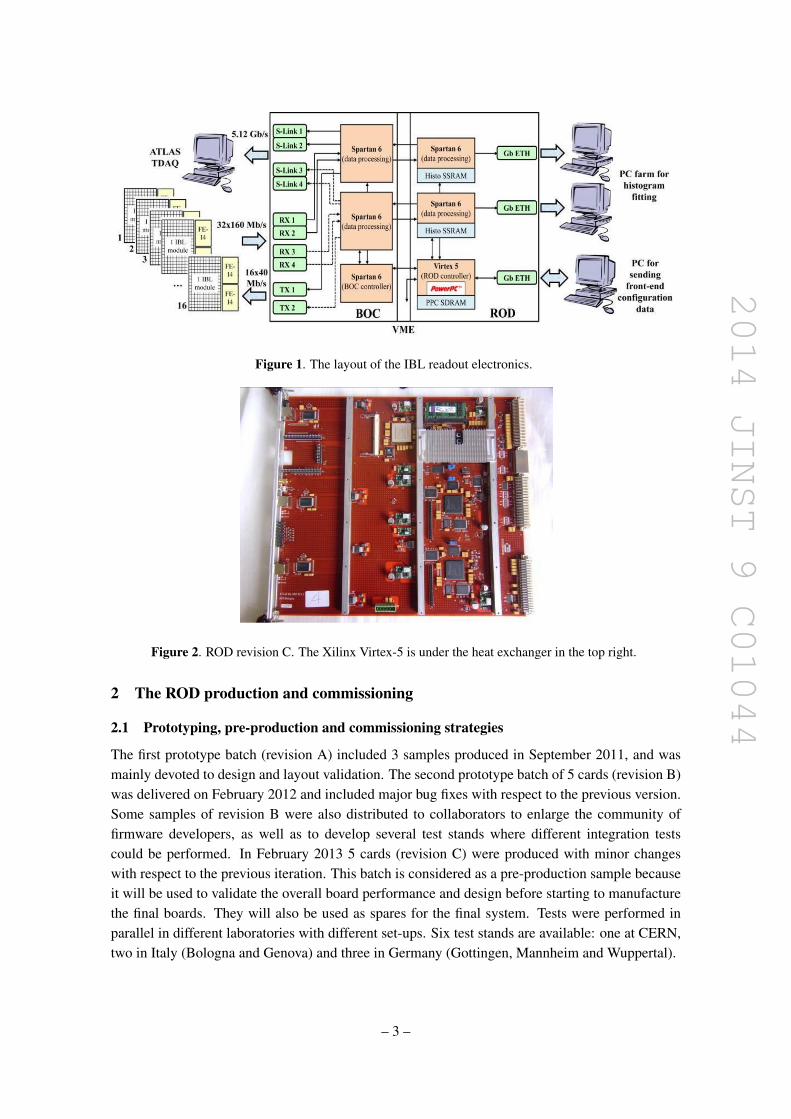
2014 JINST 9 C01044
22 ROD testing
As part of testing the prototype boards we have developed a comprehensive set of tests for boardbring-up and deployment The list of features that must be verified is the following
bull VME interface
bull FPGA firmware download both stand-alone and from VME
bull FPGA-embedded processors with software download from VME
bull TIM2 interface (VME module which connects with the ATLAS level-1 trigger system)
bull connectivity between FPGAs and memory components (DDR2 FLASH-based SynchronousStatic RAM)
bull three Gigabit Ethernet links
bull ROD bus (asynchronous bus to configure chips on both ROD and BOC)
bull buses to and from the BOC
Three specific tests will be discussed in the following as being particularly interesting In thefirst we will show how testing prototypes was decisive on finalizing some layout options in thesecond we will spotlight one typical case where complex approaches and custom solutions havebeen developed to face a quite difficult problem The last example will spotlight how integrationtests provided us reasonable confidence that the ROD required performance has been successfullyaccomplished
221 Test example 1 BOC to ROD transmission
The data received by the BOC from the FE-I4 after decoding is sent to the ROD via a 96-bit widebus with a single line signal rate of 80 Mbs The bus width and the signal rate have been dimen-sioned as a tradeoff between the bandwidth requirement between BOC and ROD (512 Gbs) andthe design modularity (12 bit is the width of the front-end data) The bus connects the Spartan-6FPGAs hosted on the different cards through the VME backplane connectors The communicationhas been implemented with the SSTL 3 standard [9] Transmission is double data rate synchro-nized with the 40 MHz clock common to both cards The bus has been designed to have minimalskew and to optimize the signal integrity in the PCB layout The decision whether to include busterminators external to the FPGA was postponed to a later stage terminations provide better signalintegrity but the increased routing congestion and the reduced space on the board have to be con-sidered Extensive tests have been performed with an ad-hoc firmware sending data continuouslyand measuring the bit error rate by varying the phase of the receiver clock The goal of this test wasto measure the width of the good sampling phase window A typical result for cards of revisions Aand B is shown in table 1
2The TIM (TTC Interface Module) is a VME board that distributes clock and trigger signals received from theTiming Trigger and Control (TTC) system to the cards hosted into the crate
ndash 4 ndash
2014 JINST 9 C01044
Table 1 Typical results for the BOC to ROD communication with revision B cards Different phases ofthe clock at the receiver side are tested Each value has been verified by sending data formatted as 12-bitfree-running counters continuously for 2 hours
Phase (degrees) Device Status Problems
0SP6A FAIL Multiple errors on every busSP6B FAIL Multiple errors on every bus
90SP6A FAIL Multiple errors on A busSP6B FAIL Multiple errors on B bus
180SP6A FAIL Sometimes read C8 instead of CC on A busSP6B OK
270SP6A OKSP6B OK
Table 2 Example of results for the BOC to ROD transmission with revision C cards The same patterns andduration as in table 1 have been used
Phase (degrees) Device Status Problems
0SP6A FAIL Multiple errors on every busSP6B FAIL Multiple errors on every bus
90SP6A FAIL One error in 2 hours of testSP6B OK
180SP6A OKSP6B OK
270SP6A OKSP6B OK
Due to unsatisfactory results we added compact package resistors onto the whole bus in re-vision C taking care to minimize changes on the current signal routing The result for one card isshown in table 2 The performance looked more satisfactory and we have seen good uniformitybetween cards
222 Test example 2 SRAM controller for calibration histograms
As it was previously mentioned (section 13) one of the tasks of the ROD card is to create his-tograms of the data for calibrating the detector Preliminary estimates show how scans whichrequired about 10 minutes with the existing electronics can be performed faster in the IBL RODSince the histograms are read-out via Gigabit Ethernet links acquisition runs with a comparableamount of data can be accomplished in about 10 seconds The most important speed limitation be-comes the maximum data rate of the Synchronous Static RAM (SSRAM) components Due to thecard design in order to manage histograms for all FE-I4s in parallel the selected SSRAM3 must beaccessed with a clock frequency of about 200 MHz Implementing such a 36-bit SSRAM controller
31Mx36 bit Synchronous Static RAM chips (Cypress CY7C1370D-250AXC-ND)
ndash 5 ndash
2014 JINST 9 C01044
running at 200 MHz in a Spartan-6 FPGA required adopting careful design techniques First theclock is forwarded to the SSRAM with matched PCB feedback paths Second the Spartan-6 PLLsare configured in ldquoZero delay bufferrdquo mode synchronizing both FPGA and SSRAM clocks Lastdistinct clock domains for the transmitter and receiver logic are implemented
Other issues have to be taken into account For IO pin driver properties carefully chosenvalues of both slew rate and current drive capability must be determined to get the fastest pad prop-agation delay without violating the maximum amount of simultaneous switching outputs allowedby the FPGAs
Finally effects due to bus contention have been evaluated This happens when two devicesare simultaneously driving a bi-directional line This is exacerbated by clock skew between thetransmitter and receiver elements Bus contention increases the power dissipation of the compo-nents Taking into account both the switching times of devices (from the datasheets) and relativeclock phases (from simulation) a temperature rise of less than 3C has been expected Even thoughit is a small effect we can reduce the effect further by grouping together several cycles with thesame access type (read or write) Tests have been performed at maximum achieved clock speed(200 MHz) measuring the increase of temperature (with a thermal camera) and showing that wesucceeded on limiting that effect
The interface with the SSRAM has been successfully tested at 200 MHz in stand-alone op-eration while a 140 MHz working version has been proven to work when integrated in the latestofficial release of the ROD firmware
223 Test example 3 integration with the FE-I4
Extensive tests have been performed connecting the FE-I4 to a BOC-ROD pair Their major aimis to validate the resources implemented on both cards (eg the amount of memory available in thechosen components) showing that hardware specifications have been met Moreover integrationtests have been performed to drive the firmware design and development with real use cases
The official version of the firmware is shown in figure 3 The design is highly modular Fourgroups of 8 FE-I4 (4 modules) are processed independently on the BOC and then transmitted to acollector block in the ROD (called the ldquogathererrdquo) Then an event builder (EFB) multiplexes databoth to an S-Link interface and to a dedicated component (called histogrammer) that accumulatesevents and fills summary histograms (occupancy time over threshold ToT per pixel ToT2 perpixel) The histogrammer stores temporary data in the SSRAMs At the end of the acquisition thehistograms are read by an embedded microcontroller (a Xilinx MicroBlaze IP core) via DMA andloaded into the DDR2 They are then sent to an external PC farm through Gigabit Ethernet linkThe PowerPC microcontroller embedded in the ROD Virtex-5 controls all the subsystems and actsas an interface to the software application that executes this test At the present time the test standis composed by two FE-I4s connected to the same datapath (see green lines in figure 3)
The results are satisfactory the basic implemented functionalities are adequate to successfullyperform data acquisition and calibration scans with FPGA resource utilization of less than 20This allows us to be confident that a more realistic version (with busy logic timeouts completeerror handling etc) will fit on the chip Moreover the whole mechanism of histogram filling andacquisition has been evaluated showing how all requirements will be met even when it will operate
ndash 6 ndash
2014 JINST 9 C01044
Figure 3 Schematic layout of the BOC-ROD firmware Only one Spartan-6 for both BOC and ROD areshown the others have an identical design The green lines represent the data paths currently under test Theorange lines indicate the ROD bus for configuring and monitoring the processing blocks
with the full set of FE-I4s connected Thus the choice of the specific components installed in theROD has been confirmed and the overall board design validated
23 ROD production plans and validation procedures
At the present time the ROD design has been successfully validated and readied for production forIBL The same firm that delivered all prototype batches will do the PCB manufacturing and assem-bly After production preliminary tests (similar to those of revision B and C) will be delegated tothe same company electrical examination after components supply and Xray inspection for largeBGA-packaged devices
We also defined a list of minimal procedures to validate the ROD cards after production
bull firmware-software upload from VME JTAG and Gigabit Ethernet ports
bull ROD to BOC (and BOC to ROD) dataflow over all IO lines
bull RW tests for Virtex-5 and Spartan-6 external memory modules
bull dataflow tests on the 3 Ethernet ports
bull TIM card connectivity test
ndash 7 ndash
2014 JINST 9 C01044
Figure 4 Synchronization errors in runs acquired last year The y-axis is the maximum number of modulesthat showed synchronization errors at a given event The ROD verifies the synchronization of the data linkby checking both encoded data format and the event counter The synchronization during data taking isautomatically restored by issuing an event counter reset every few seconds As an example a ldquoSynchroniza-tion ErrorEventrdquo of 50 means that an inefficiency of 50 out of 1700 (the number of modules in Layer 2)occurred for few seconds The excess shown by Layer 2 links with respect to the others are probably due tobandwidth limitation
These tests will be performed before the board installation on the experiment The firm hasbeen hired to produce 15 cards identical to revision C at the end of August 2013 fulfilling theproduction requirements for IBL Delivery is expected by mid October
3 Review on upgrade for read-out electronics of Layer 1 and Layer 2
With the restart of LHC (2014) we are expecting a higher luminosity which will increase evenmore in subsequent years As a consequence we foresee that the Pixel readout link of the actualdetector will suffer from bandwidth limitations The link bandwidth is proportional to the productof occupancy and trigger rate of the front-end devices The first is a function of the luminosity andcan be extrapolated using the experience gained from previous years of data acquisition Prelimi-nary measurements show that even with an average number of expected pile-up events 〈micro〉 asymp 50(a reasonable estimation for luminosity energy and bunch spacing expected by 2015) and triggerrate of 100 kHz the estimated average link occupancy for Layer 2 is about 90
With greater pile-up (when luminosity will be greater than 2 middot 1034 cmminus2 sminus1) even Layer 1will get into trouble Moreover in the last run Layer 2 already showed several synchronizationerrors probably due to bandwidth limitation even though the average link occupancy was about50 (figure 4)
The actions that could be taken are different in Layer 1 and Layer 2 Layer 2 is read-out withone link per module at 40 Mbs Increasing the bandwidth to 80 Mbs is a viable solution it wouldrequire producing more BOC opto-electrical plug-ins as well as more BOC-ROD pairs (to support
ndash 8 ndash
2014 JINST 9 C01044
double the bandwidth) and rearranging the link cabling Since IBL off-detector electronics alreadymanage BOC-ROD transmissions at 80 Mbs (section 4) it would be straightforward to adopt IBLcards Only two minor modifications would be needed a new firmware and new custom RX opto-electrical BOC plug-ins No change in connectivity and fiber routing is foreseen
Layer 1 is already able to manage read-out at 80 Mbs therefore installing a second link permodule can increase the bandwidth As in the previous case the adoption of IBL cards wouldrequire both new firmware and BOC plug-ins with minor modifications of the connections
The adoption of IBL ROD-BOC cards would bring also more benefits because of the stan-dardized design it will provide a uniform board for most of the Pixel read-out system and providecommon spares for all sub-detectors No modifications will be needed to the ROD design so pro-duction can start immediately and the board will be ready by the LHC restart 26 ROD will beneeded for Layer 2 and 38 for Layer 1 No official decisions on board deployment have been takenyet but discussions are ongoing
References
[1] ATLAS collaboration The ATLAS experiment at the CERN Large Hadron Collider2008 JINST 3 S08003
[2] G Aad et al ATLAS pixel detector electronics and sensors 2008 JINST 3 P07007
[3] ATLAS collaboration ATLAS Insertable B-Layer technical design report CERN-LHCC-2010-013
[4] ATLAS IBL collaboration Prototype ATLAS IBL modules using the FE-I4A front-end readout chip2012 JINST 7 P11010
[5] J Dopke et al The IBL readout system 2011 JINST 6 C01006
[6] M Wensing Testing and firmware development for the ATLAS IBL BOC prototype2012 JINST 7 C12027
[7] HC van der Bij et al S-LINK a prototype of the ATLAS read-out link in Proceedings of the FourthWorkshop on Electronics for LHC Experiments Rome Italy 21ndash25 Sep 1998
[8] G Balbi et al Implementation and tests of FPGA-embedded PowerPC in the control system of theATLAS IBL ROD card 2013 JINST 8 C01012
[9] JEDEC Solid State Technology Association Stub-series terminated logic for 33 volts (SSTL 3)JESD8-8 (1996)
ndash 9 ndash
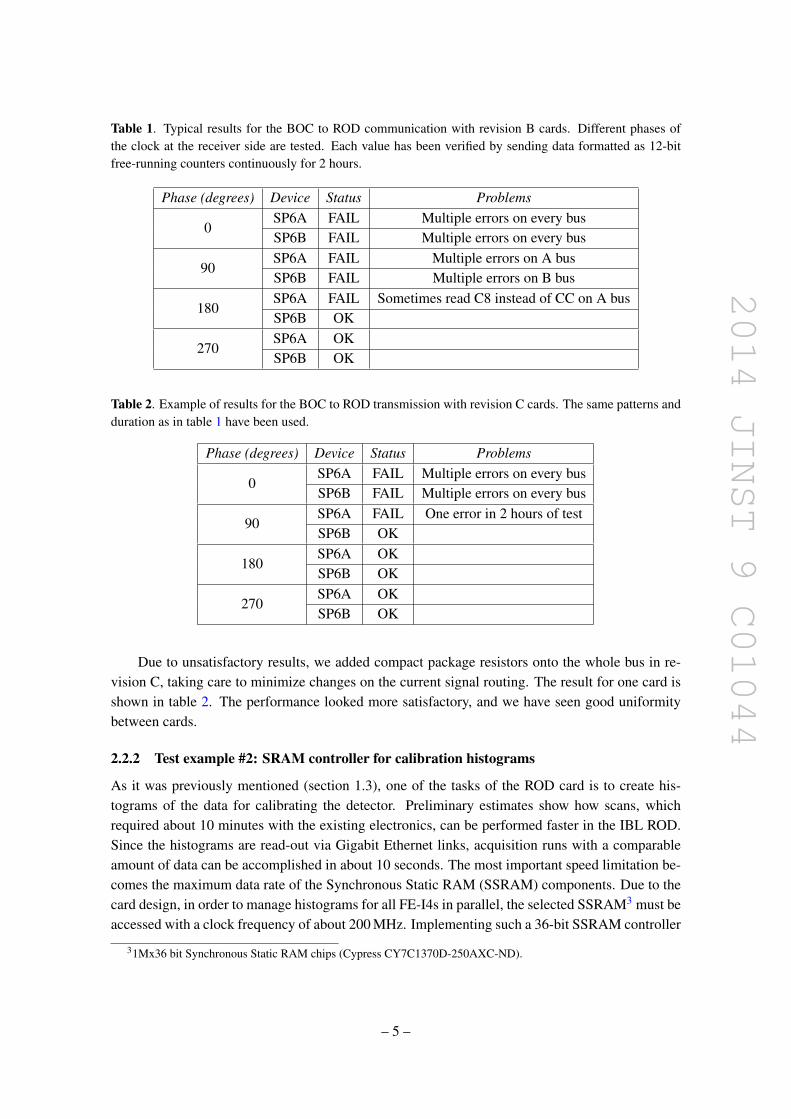
2014 JINST 9 C01044
Table 1 Typical results for the BOC to ROD communication with revision B cards Different phases ofthe clock at the receiver side are tested Each value has been verified by sending data formatted as 12-bitfree-running counters continuously for 2 hours
Phase (degrees) Device Status Problems
0SP6A FAIL Multiple errors on every busSP6B FAIL Multiple errors on every bus
90SP6A FAIL Multiple errors on A busSP6B FAIL Multiple errors on B bus
180SP6A FAIL Sometimes read C8 instead of CC on A busSP6B OK
270SP6A OKSP6B OK
Table 2 Example of results for the BOC to ROD transmission with revision C cards The same patterns andduration as in table 1 have been used
Phase (degrees) Device Status Problems
0SP6A FAIL Multiple errors on every busSP6B FAIL Multiple errors on every bus
90SP6A FAIL One error in 2 hours of testSP6B OK
180SP6A OKSP6B OK
270SP6A OKSP6B OK
Due to unsatisfactory results we added compact package resistors onto the whole bus in re-vision C taking care to minimize changes on the current signal routing The result for one card isshown in table 2 The performance looked more satisfactory and we have seen good uniformitybetween cards
222 Test example 2 SRAM controller for calibration histograms
As it was previously mentioned (section 13) one of the tasks of the ROD card is to create his-tograms of the data for calibrating the detector Preliminary estimates show how scans whichrequired about 10 minutes with the existing electronics can be performed faster in the IBL RODSince the histograms are read-out via Gigabit Ethernet links acquisition runs with a comparableamount of data can be accomplished in about 10 seconds The most important speed limitation be-comes the maximum data rate of the Synchronous Static RAM (SSRAM) components Due to thecard design in order to manage histograms for all FE-I4s in parallel the selected SSRAM3 must beaccessed with a clock frequency of about 200 MHz Implementing such a 36-bit SSRAM controller
31Mx36 bit Synchronous Static RAM chips (Cypress CY7C1370D-250AXC-ND)
ndash 5 ndash
2014 JINST 9 C01044
running at 200 MHz in a Spartan-6 FPGA required adopting careful design techniques First theclock is forwarded to the SSRAM with matched PCB feedback paths Second the Spartan-6 PLLsare configured in ldquoZero delay bufferrdquo mode synchronizing both FPGA and SSRAM clocks Lastdistinct clock domains for the transmitter and receiver logic are implemented
Other issues have to be taken into account For IO pin driver properties carefully chosenvalues of both slew rate and current drive capability must be determined to get the fastest pad prop-agation delay without violating the maximum amount of simultaneous switching outputs allowedby the FPGAs
Finally effects due to bus contention have been evaluated This happens when two devicesare simultaneously driving a bi-directional line This is exacerbated by clock skew between thetransmitter and receiver elements Bus contention increases the power dissipation of the compo-nents Taking into account both the switching times of devices (from the datasheets) and relativeclock phases (from simulation) a temperature rise of less than 3C has been expected Even thoughit is a small effect we can reduce the effect further by grouping together several cycles with thesame access type (read or write) Tests have been performed at maximum achieved clock speed(200 MHz) measuring the increase of temperature (with a thermal camera) and showing that wesucceeded on limiting that effect
The interface with the SSRAM has been successfully tested at 200 MHz in stand-alone op-eration while a 140 MHz working version has been proven to work when integrated in the latestofficial release of the ROD firmware
223 Test example 3 integration with the FE-I4
Extensive tests have been performed connecting the FE-I4 to a BOC-ROD pair Their major aimis to validate the resources implemented on both cards (eg the amount of memory available in thechosen components) showing that hardware specifications have been met Moreover integrationtests have been performed to drive the firmware design and development with real use cases
The official version of the firmware is shown in figure 3 The design is highly modular Fourgroups of 8 FE-I4 (4 modules) are processed independently on the BOC and then transmitted to acollector block in the ROD (called the ldquogathererrdquo) Then an event builder (EFB) multiplexes databoth to an S-Link interface and to a dedicated component (called histogrammer) that accumulatesevents and fills summary histograms (occupancy time over threshold ToT per pixel ToT2 perpixel) The histogrammer stores temporary data in the SSRAMs At the end of the acquisition thehistograms are read by an embedded microcontroller (a Xilinx MicroBlaze IP core) via DMA andloaded into the DDR2 They are then sent to an external PC farm through Gigabit Ethernet linkThe PowerPC microcontroller embedded in the ROD Virtex-5 controls all the subsystems and actsas an interface to the software application that executes this test At the present time the test standis composed by two FE-I4s connected to the same datapath (see green lines in figure 3)
The results are satisfactory the basic implemented functionalities are adequate to successfullyperform data acquisition and calibration scans with FPGA resource utilization of less than 20This allows us to be confident that a more realistic version (with busy logic timeouts completeerror handling etc) will fit on the chip Moreover the whole mechanism of histogram filling andacquisition has been evaluated showing how all requirements will be met even when it will operate
ndash 6 ndash
2014 JINST 9 C01044
Figure 3 Schematic layout of the BOC-ROD firmware Only one Spartan-6 for both BOC and ROD areshown the others have an identical design The green lines represent the data paths currently under test Theorange lines indicate the ROD bus for configuring and monitoring the processing blocks
with the full set of FE-I4s connected Thus the choice of the specific components installed in theROD has been confirmed and the overall board design validated
23 ROD production plans and validation procedures
At the present time the ROD design has been successfully validated and readied for production forIBL The same firm that delivered all prototype batches will do the PCB manufacturing and assem-bly After production preliminary tests (similar to those of revision B and C) will be delegated tothe same company electrical examination after components supply and Xray inspection for largeBGA-packaged devices
We also defined a list of minimal procedures to validate the ROD cards after production
bull firmware-software upload from VME JTAG and Gigabit Ethernet ports
bull ROD to BOC (and BOC to ROD) dataflow over all IO lines
bull RW tests for Virtex-5 and Spartan-6 external memory modules
bull dataflow tests on the 3 Ethernet ports
bull TIM card connectivity test
ndash 7 ndash
2014 JINST 9 C01044
Figure 4 Synchronization errors in runs acquired last year The y-axis is the maximum number of modulesthat showed synchronization errors at a given event The ROD verifies the synchronization of the data linkby checking both encoded data format and the event counter The synchronization during data taking isautomatically restored by issuing an event counter reset every few seconds As an example a ldquoSynchroniza-tion ErrorEventrdquo of 50 means that an inefficiency of 50 out of 1700 (the number of modules in Layer 2)occurred for few seconds The excess shown by Layer 2 links with respect to the others are probably due tobandwidth limitation
These tests will be performed before the board installation on the experiment The firm hasbeen hired to produce 15 cards identical to revision C at the end of August 2013 fulfilling theproduction requirements for IBL Delivery is expected by mid October
3 Review on upgrade for read-out electronics of Layer 1 and Layer 2
With the restart of LHC (2014) we are expecting a higher luminosity which will increase evenmore in subsequent years As a consequence we foresee that the Pixel readout link of the actualdetector will suffer from bandwidth limitations The link bandwidth is proportional to the productof occupancy and trigger rate of the front-end devices The first is a function of the luminosity andcan be extrapolated using the experience gained from previous years of data acquisition Prelimi-nary measurements show that even with an average number of expected pile-up events 〈micro〉 asymp 50(a reasonable estimation for luminosity energy and bunch spacing expected by 2015) and triggerrate of 100 kHz the estimated average link occupancy for Layer 2 is about 90
With greater pile-up (when luminosity will be greater than 2 middot 1034 cmminus2 sminus1) even Layer 1will get into trouble Moreover in the last run Layer 2 already showed several synchronizationerrors probably due to bandwidth limitation even though the average link occupancy was about50 (figure 4)
The actions that could be taken are different in Layer 1 and Layer 2 Layer 2 is read-out withone link per module at 40 Mbs Increasing the bandwidth to 80 Mbs is a viable solution it wouldrequire producing more BOC opto-electrical plug-ins as well as more BOC-ROD pairs (to support
ndash 8 ndash
2014 JINST 9 C01044
double the bandwidth) and rearranging the link cabling Since IBL off-detector electronics alreadymanage BOC-ROD transmissions at 80 Mbs (section 4) it would be straightforward to adopt IBLcards Only two minor modifications would be needed a new firmware and new custom RX opto-electrical BOC plug-ins No change in connectivity and fiber routing is foreseen
Layer 1 is already able to manage read-out at 80 Mbs therefore installing a second link permodule can increase the bandwidth As in the previous case the adoption of IBL cards wouldrequire both new firmware and BOC plug-ins with minor modifications of the connections
The adoption of IBL ROD-BOC cards would bring also more benefits because of the stan-dardized design it will provide a uniform board for most of the Pixel read-out system and providecommon spares for all sub-detectors No modifications will be needed to the ROD design so pro-duction can start immediately and the board will be ready by the LHC restart 26 ROD will beneeded for Layer 2 and 38 for Layer 1 No official decisions on board deployment have been takenyet but discussions are ongoing
References
[1] ATLAS collaboration The ATLAS experiment at the CERN Large Hadron Collider2008 JINST 3 S08003
[2] G Aad et al ATLAS pixel detector electronics and sensors 2008 JINST 3 P07007
[3] ATLAS collaboration ATLAS Insertable B-Layer technical design report CERN-LHCC-2010-013
[4] ATLAS IBL collaboration Prototype ATLAS IBL modules using the FE-I4A front-end readout chip2012 JINST 7 P11010
[5] J Dopke et al The IBL readout system 2011 JINST 6 C01006
[6] M Wensing Testing and firmware development for the ATLAS IBL BOC prototype2012 JINST 7 C12027
[7] HC van der Bij et al S-LINK a prototype of the ATLAS read-out link in Proceedings of the FourthWorkshop on Electronics for LHC Experiments Rome Italy 21ndash25 Sep 1998
[8] G Balbi et al Implementation and tests of FPGA-embedded PowerPC in the control system of theATLAS IBL ROD card 2013 JINST 8 C01012
[9] JEDEC Solid State Technology Association Stub-series terminated logic for 33 volts (SSTL 3)JESD8-8 (1996)
ndash 9 ndash
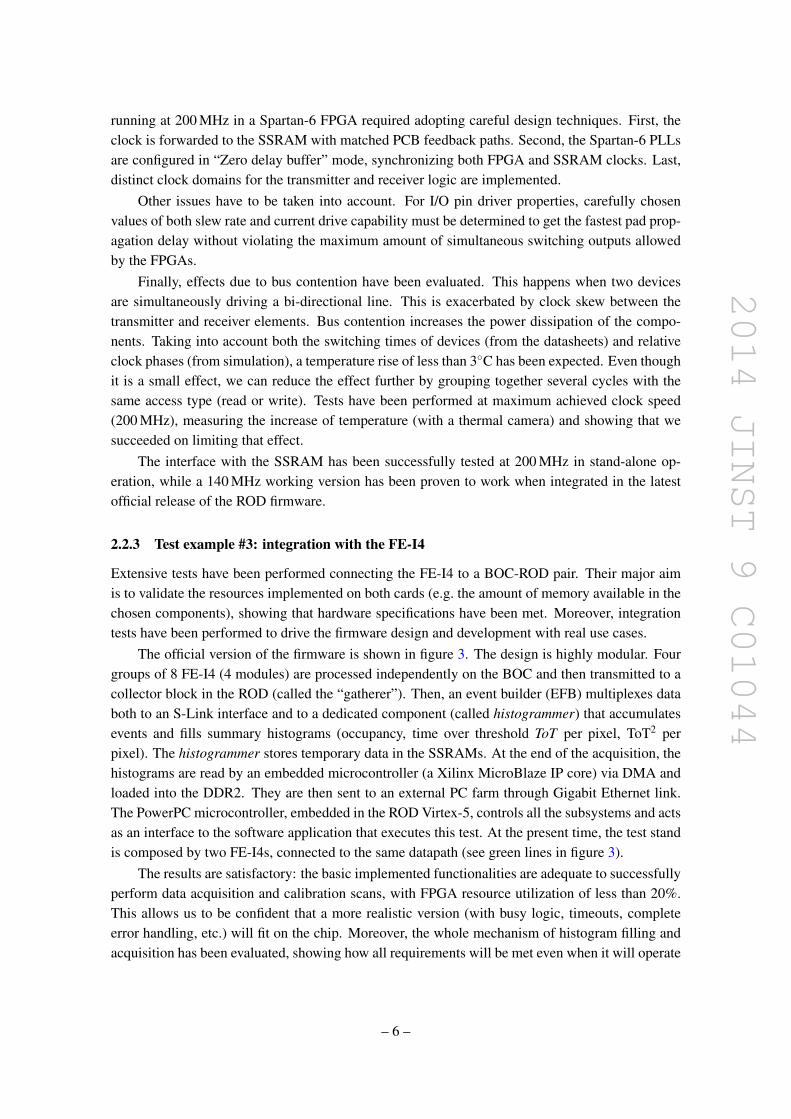
2014 JINST 9 C01044
running at 200 MHz in a Spartan-6 FPGA required adopting careful design techniques First theclock is forwarded to the SSRAM with matched PCB feedback paths Second the Spartan-6 PLLsare configured in ldquoZero delay bufferrdquo mode synchronizing both FPGA and SSRAM clocks Lastdistinct clock domains for the transmitter and receiver logic are implemented
Other issues have to be taken into account For IO pin driver properties carefully chosenvalues of both slew rate and current drive capability must be determined to get the fastest pad prop-agation delay without violating the maximum amount of simultaneous switching outputs allowedby the FPGAs
Finally effects due to bus contention have been evaluated This happens when two devicesare simultaneously driving a bi-directional line This is exacerbated by clock skew between thetransmitter and receiver elements Bus contention increases the power dissipation of the compo-nents Taking into account both the switching times of devices (from the datasheets) and relativeclock phases (from simulation) a temperature rise of less than 3C has been expected Even thoughit is a small effect we can reduce the effect further by grouping together several cycles with thesame access type (read or write) Tests have been performed at maximum achieved clock speed(200 MHz) measuring the increase of temperature (with a thermal camera) and showing that wesucceeded on limiting that effect
The interface with the SSRAM has been successfully tested at 200 MHz in stand-alone op-eration while a 140 MHz working version has been proven to work when integrated in the latestofficial release of the ROD firmware
223 Test example 3 integration with the FE-I4
Extensive tests have been performed connecting the FE-I4 to a BOC-ROD pair Their major aimis to validate the resources implemented on both cards (eg the amount of memory available in thechosen components) showing that hardware specifications have been met Moreover integrationtests have been performed to drive the firmware design and development with real use cases
The official version of the firmware is shown in figure 3 The design is highly modular Fourgroups of 8 FE-I4 (4 modules) are processed independently on the BOC and then transmitted to acollector block in the ROD (called the ldquogathererrdquo) Then an event builder (EFB) multiplexes databoth to an S-Link interface and to a dedicated component (called histogrammer) that accumulatesevents and fills summary histograms (occupancy time over threshold ToT per pixel ToT2 perpixel) The histogrammer stores temporary data in the SSRAMs At the end of the acquisition thehistograms are read by an embedded microcontroller (a Xilinx MicroBlaze IP core) via DMA andloaded into the DDR2 They are then sent to an external PC farm through Gigabit Ethernet linkThe PowerPC microcontroller embedded in the ROD Virtex-5 controls all the subsystems and actsas an interface to the software application that executes this test At the present time the test standis composed by two FE-I4s connected to the same datapath (see green lines in figure 3)
The results are satisfactory the basic implemented functionalities are adequate to successfullyperform data acquisition and calibration scans with FPGA resource utilization of less than 20This allows us to be confident that a more realistic version (with busy logic timeouts completeerror handling etc) will fit on the chip Moreover the whole mechanism of histogram filling andacquisition has been evaluated showing how all requirements will be met even when it will operate
ndash 6 ndash
2014 JINST 9 C01044
Figure 3 Schematic layout of the BOC-ROD firmware Only one Spartan-6 for both BOC and ROD areshown the others have an identical design The green lines represent the data paths currently under test Theorange lines indicate the ROD bus for configuring and monitoring the processing blocks
with the full set of FE-I4s connected Thus the choice of the specific components installed in theROD has been confirmed and the overall board design validated
23 ROD production plans and validation procedures
At the present time the ROD design has been successfully validated and readied for production forIBL The same firm that delivered all prototype batches will do the PCB manufacturing and assem-bly After production preliminary tests (similar to those of revision B and C) will be delegated tothe same company electrical examination after components supply and Xray inspection for largeBGA-packaged devices
We also defined a list of minimal procedures to validate the ROD cards after production
bull firmware-software upload from VME JTAG and Gigabit Ethernet ports
bull ROD to BOC (and BOC to ROD) dataflow over all IO lines
bull RW tests for Virtex-5 and Spartan-6 external memory modules
bull dataflow tests on the 3 Ethernet ports
bull TIM card connectivity test
ndash 7 ndash
2014 JINST 9 C01044
Figure 4 Synchronization errors in runs acquired last year The y-axis is the maximum number of modulesthat showed synchronization errors at a given event The ROD verifies the synchronization of the data linkby checking both encoded data format and the event counter The synchronization during data taking isautomatically restored by issuing an event counter reset every few seconds As an example a ldquoSynchroniza-tion ErrorEventrdquo of 50 means that an inefficiency of 50 out of 1700 (the number of modules in Layer 2)occurred for few seconds The excess shown by Layer 2 links with respect to the others are probably due tobandwidth limitation
These tests will be performed before the board installation on the experiment The firm hasbeen hired to produce 15 cards identical to revision C at the end of August 2013 fulfilling theproduction requirements for IBL Delivery is expected by mid October
3 Review on upgrade for read-out electronics of Layer 1 and Layer 2
With the restart of LHC (2014) we are expecting a higher luminosity which will increase evenmore in subsequent years As a consequence we foresee that the Pixel readout link of the actualdetector will suffer from bandwidth limitations The link bandwidth is proportional to the productof occupancy and trigger rate of the front-end devices The first is a function of the luminosity andcan be extrapolated using the experience gained from previous years of data acquisition Prelimi-nary measurements show that even with an average number of expected pile-up events 〈micro〉 asymp 50(a reasonable estimation for luminosity energy and bunch spacing expected by 2015) and triggerrate of 100 kHz the estimated average link occupancy for Layer 2 is about 90
With greater pile-up (when luminosity will be greater than 2 middot 1034 cmminus2 sminus1) even Layer 1will get into trouble Moreover in the last run Layer 2 already showed several synchronizationerrors probably due to bandwidth limitation even though the average link occupancy was about50 (figure 4)
The actions that could be taken are different in Layer 1 and Layer 2 Layer 2 is read-out withone link per module at 40 Mbs Increasing the bandwidth to 80 Mbs is a viable solution it wouldrequire producing more BOC opto-electrical plug-ins as well as more BOC-ROD pairs (to support
ndash 8 ndash
2014 JINST 9 C01044
double the bandwidth) and rearranging the link cabling Since IBL off-detector electronics alreadymanage BOC-ROD transmissions at 80 Mbs (section 4) it would be straightforward to adopt IBLcards Only two minor modifications would be needed a new firmware and new custom RX opto-electrical BOC plug-ins No change in connectivity and fiber routing is foreseen
Layer 1 is already able to manage read-out at 80 Mbs therefore installing a second link permodule can increase the bandwidth As in the previous case the adoption of IBL cards wouldrequire both new firmware and BOC plug-ins with minor modifications of the connections
The adoption of IBL ROD-BOC cards would bring also more benefits because of the stan-dardized design it will provide a uniform board for most of the Pixel read-out system and providecommon spares for all sub-detectors No modifications will be needed to the ROD design so pro-duction can start immediately and the board will be ready by the LHC restart 26 ROD will beneeded for Layer 2 and 38 for Layer 1 No official decisions on board deployment have been takenyet but discussions are ongoing
References
[1] ATLAS collaboration The ATLAS experiment at the CERN Large Hadron Collider2008 JINST 3 S08003
[2] G Aad et al ATLAS pixel detector electronics and sensors 2008 JINST 3 P07007
[3] ATLAS collaboration ATLAS Insertable B-Layer technical design report CERN-LHCC-2010-013
[4] ATLAS IBL collaboration Prototype ATLAS IBL modules using the FE-I4A front-end readout chip2012 JINST 7 P11010
[5] J Dopke et al The IBL readout system 2011 JINST 6 C01006
[6] M Wensing Testing and firmware development for the ATLAS IBL BOC prototype2012 JINST 7 C12027
[7] HC van der Bij et al S-LINK a prototype of the ATLAS read-out link in Proceedings of the FourthWorkshop on Electronics for LHC Experiments Rome Italy 21ndash25 Sep 1998
[8] G Balbi et al Implementation and tests of FPGA-embedded PowerPC in the control system of theATLAS IBL ROD card 2013 JINST 8 C01012
[9] JEDEC Solid State Technology Association Stub-series terminated logic for 33 volts (SSTL 3)JESD8-8 (1996)
ndash 9 ndash
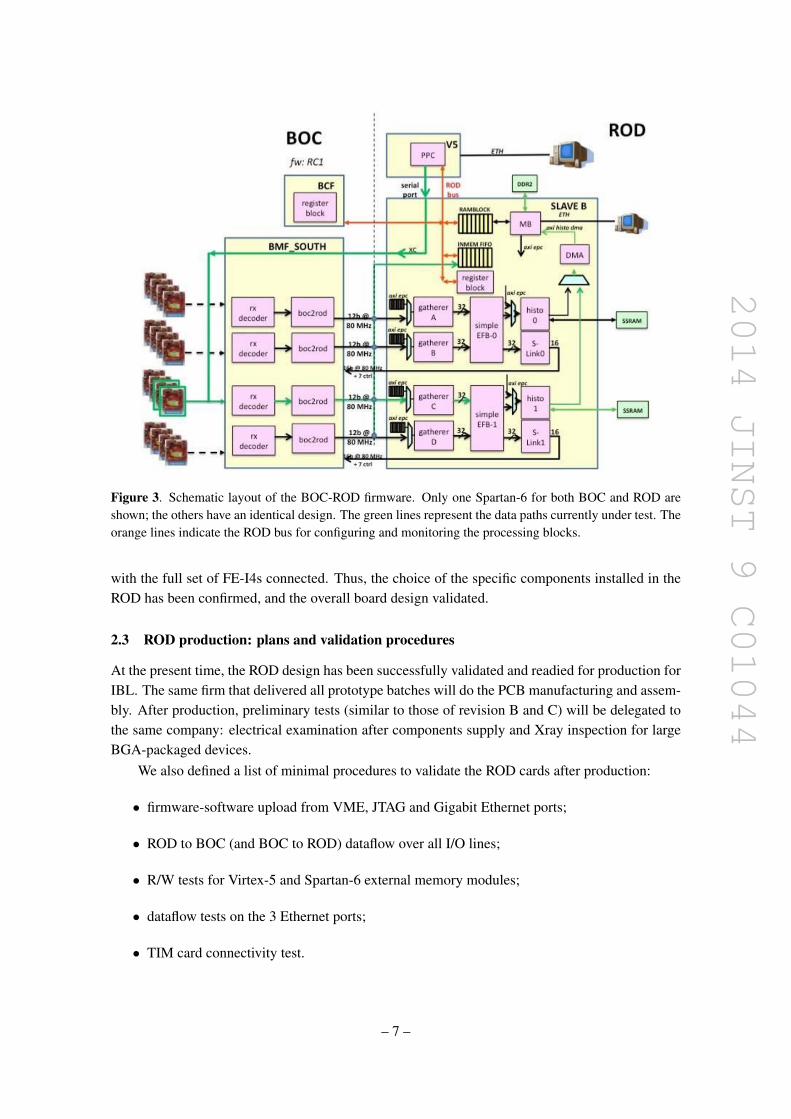
2014 JINST 9 C01044
Figure 3 Schematic layout of the BOC-ROD firmware Only one Spartan-6 for both BOC and ROD areshown the others have an identical design The green lines represent the data paths currently under test Theorange lines indicate the ROD bus for configuring and monitoring the processing blocks
with the full set of FE-I4s connected Thus the choice of the specific components installed in theROD has been confirmed and the overall board design validated
23 ROD production plans and validation procedures
At the present time the ROD design has been successfully validated and readied for production forIBL The same firm that delivered all prototype batches will do the PCB manufacturing and assem-bly After production preliminary tests (similar to those of revision B and C) will be delegated tothe same company electrical examination after components supply and Xray inspection for largeBGA-packaged devices
We also defined a list of minimal procedures to validate the ROD cards after production
bull firmware-software upload from VME JTAG and Gigabit Ethernet ports
bull ROD to BOC (and BOC to ROD) dataflow over all IO lines
bull RW tests for Virtex-5 and Spartan-6 external memory modules
bull dataflow tests on the 3 Ethernet ports
bull TIM card connectivity test
ndash 7 ndash
2014 JINST 9 C01044
Figure 4 Synchronization errors in runs acquired last year The y-axis is the maximum number of modulesthat showed synchronization errors at a given event The ROD verifies the synchronization of the data linkby checking both encoded data format and the event counter The synchronization during data taking isautomatically restored by issuing an event counter reset every few seconds As an example a ldquoSynchroniza-tion ErrorEventrdquo of 50 means that an inefficiency of 50 out of 1700 (the number of modules in Layer 2)occurred for few seconds The excess shown by Layer 2 links with respect to the others are probably due tobandwidth limitation
These tests will be performed before the board installation on the experiment The firm hasbeen hired to produce 15 cards identical to revision C at the end of August 2013 fulfilling theproduction requirements for IBL Delivery is expected by mid October
3 Review on upgrade for read-out electronics of Layer 1 and Layer 2
With the restart of LHC (2014) we are expecting a higher luminosity which will increase evenmore in subsequent years As a consequence we foresee that the Pixel readout link of the actualdetector will suffer from bandwidth limitations The link bandwidth is proportional to the productof occupancy and trigger rate of the front-end devices The first is a function of the luminosity andcan be extrapolated using the experience gained from previous years of data acquisition Prelimi-nary measurements show that even with an average number of expected pile-up events 〈micro〉 asymp 50(a reasonable estimation for luminosity energy and bunch spacing expected by 2015) and triggerrate of 100 kHz the estimated average link occupancy for Layer 2 is about 90
With greater pile-up (when luminosity will be greater than 2 middot 1034 cmminus2 sminus1) even Layer 1will get into trouble Moreover in the last run Layer 2 already showed several synchronizationerrors probably due to bandwidth limitation even though the average link occupancy was about50 (figure 4)
The actions that could be taken are different in Layer 1 and Layer 2 Layer 2 is read-out withone link per module at 40 Mbs Increasing the bandwidth to 80 Mbs is a viable solution it wouldrequire producing more BOC opto-electrical plug-ins as well as more BOC-ROD pairs (to support
ndash 8 ndash
2014 JINST 9 C01044
double the bandwidth) and rearranging the link cabling Since IBL off-detector electronics alreadymanage BOC-ROD transmissions at 80 Mbs (section 4) it would be straightforward to adopt IBLcards Only two minor modifications would be needed a new firmware and new custom RX opto-electrical BOC plug-ins No change in connectivity and fiber routing is foreseen
Layer 1 is already able to manage read-out at 80 Mbs therefore installing a second link permodule can increase the bandwidth As in the previous case the adoption of IBL cards wouldrequire both new firmware and BOC plug-ins with minor modifications of the connections
The adoption of IBL ROD-BOC cards would bring also more benefits because of the stan-dardized design it will provide a uniform board for most of the Pixel read-out system and providecommon spares for all sub-detectors No modifications will be needed to the ROD design so pro-duction can start immediately and the board will be ready by the LHC restart 26 ROD will beneeded for Layer 2 and 38 for Layer 1 No official decisions on board deployment have been takenyet but discussions are ongoing
References
[1] ATLAS collaboration The ATLAS experiment at the CERN Large Hadron Collider2008 JINST 3 S08003
[2] G Aad et al ATLAS pixel detector electronics and sensors 2008 JINST 3 P07007
[3] ATLAS collaboration ATLAS Insertable B-Layer technical design report CERN-LHCC-2010-013
[4] ATLAS IBL collaboration Prototype ATLAS IBL modules using the FE-I4A front-end readout chip2012 JINST 7 P11010
[5] J Dopke et al The IBL readout system 2011 JINST 6 C01006
[6] M Wensing Testing and firmware development for the ATLAS IBL BOC prototype2012 JINST 7 C12027
[7] HC van der Bij et al S-LINK a prototype of the ATLAS read-out link in Proceedings of the FourthWorkshop on Electronics for LHC Experiments Rome Italy 21ndash25 Sep 1998
[8] G Balbi et al Implementation and tests of FPGA-embedded PowerPC in the control system of theATLAS IBL ROD card 2013 JINST 8 C01012
[9] JEDEC Solid State Technology Association Stub-series terminated logic for 33 volts (SSTL 3)JESD8-8 (1996)
ndash 9 ndash
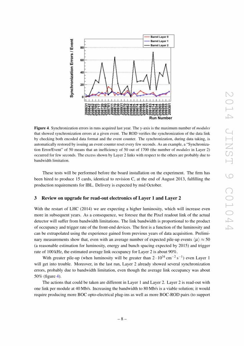
2014 JINST 9 C01044
Figure 4 Synchronization errors in runs acquired last year The y-axis is the maximum number of modulesthat showed synchronization errors at a given event The ROD verifies the synchronization of the data linkby checking both encoded data format and the event counter The synchronization during data taking isautomatically restored by issuing an event counter reset every few seconds As an example a ldquoSynchroniza-tion ErrorEventrdquo of 50 means that an inefficiency of 50 out of 1700 (the number of modules in Layer 2)occurred for few seconds The excess shown by Layer 2 links with respect to the others are probably due tobandwidth limitation
These tests will be performed before the board installation on the experiment The firm hasbeen hired to produce 15 cards identical to revision C at the end of August 2013 fulfilling theproduction requirements for IBL Delivery is expected by mid October
3 Review on upgrade for read-out electronics of Layer 1 and Layer 2
With the restart of LHC (2014) we are expecting a higher luminosity which will increase evenmore in subsequent years As a consequence we foresee that the Pixel readout link of the actualdetector will suffer from bandwidth limitations The link bandwidth is proportional to the productof occupancy and trigger rate of the front-end devices The first is a function of the luminosity andcan be extrapolated using the experience gained from previous years of data acquisition Prelimi-nary measurements show that even with an average number of expected pile-up events 〈micro〉 asymp 50(a reasonable estimation for luminosity energy and bunch spacing expected by 2015) and triggerrate of 100 kHz the estimated average link occupancy for Layer 2 is about 90
With greater pile-up (when luminosity will be greater than 2 middot 1034 cmminus2 sminus1) even Layer 1will get into trouble Moreover in the last run Layer 2 already showed several synchronizationerrors probably due to bandwidth limitation even though the average link occupancy was about50 (figure 4)
The actions that could be taken are different in Layer 1 and Layer 2 Layer 2 is read-out withone link per module at 40 Mbs Increasing the bandwidth to 80 Mbs is a viable solution it wouldrequire producing more BOC opto-electrical plug-ins as well as more BOC-ROD pairs (to support
ndash 8 ndash
2014 JINST 9 C01044
double the bandwidth) and rearranging the link cabling Since IBL off-detector electronics alreadymanage BOC-ROD transmissions at 80 Mbs (section 4) it would be straightforward to adopt IBLcards Only two minor modifications would be needed a new firmware and new custom RX opto-electrical BOC plug-ins No change in connectivity and fiber routing is foreseen
Layer 1 is already able to manage read-out at 80 Mbs therefore installing a second link permodule can increase the bandwidth As in the previous case the adoption of IBL cards wouldrequire both new firmware and BOC plug-ins with minor modifications of the connections
The adoption of IBL ROD-BOC cards would bring also more benefits because of the stan-dardized design it will provide a uniform board for most of the Pixel read-out system and providecommon spares for all sub-detectors No modifications will be needed to the ROD design so pro-duction can start immediately and the board will be ready by the LHC restart 26 ROD will beneeded for Layer 2 and 38 for Layer 1 No official decisions on board deployment have been takenyet but discussions are ongoing
References
[1] ATLAS collaboration The ATLAS experiment at the CERN Large Hadron Collider2008 JINST 3 S08003
[2] G Aad et al ATLAS pixel detector electronics and sensors 2008 JINST 3 P07007
[3] ATLAS collaboration ATLAS Insertable B-Layer technical design report CERN-LHCC-2010-013
[4] ATLAS IBL collaboration Prototype ATLAS IBL modules using the FE-I4A front-end readout chip2012 JINST 7 P11010
[5] J Dopke et al The IBL readout system 2011 JINST 6 C01006
[6] M Wensing Testing and firmware development for the ATLAS IBL BOC prototype2012 JINST 7 C12027
[7] HC van der Bij et al S-LINK a prototype of the ATLAS read-out link in Proceedings of the FourthWorkshop on Electronics for LHC Experiments Rome Italy 21ndash25 Sep 1998
[8] G Balbi et al Implementation and tests of FPGA-embedded PowerPC in the control system of theATLAS IBL ROD card 2013 JINST 8 C01012
[9] JEDEC Solid State Technology Association Stub-series terminated logic for 33 volts (SSTL 3)JESD8-8 (1996)
ndash 9 ndash