Embed Size (px)
Citation preview
The Pennsylvania State University
The Graduate School
Department of Material Science and Engineering
RESIDUAL FERROELECTRICITY, PIEZOELECTRICITY, AND
FLEXOELECTRICITY IN BARIUM STRONTIUM TITANATE TUNABLE
DIELECTRICS
A Dissertation in
Material Science and Engineering
by
Lauren M. Garten
© 2014 Lauren M. Garten
Submitted in Partial Fulfillment
of the Requirements
for the Degree of
Doctor of Philosophy
December 2014
The dissertation of Lauren M. Garten was reviewed and approved* by the following:
Susan Trolier-McKinstryProfessor of Ceramic Science and EngineeringDissertation AdvisorChair of Committee
Clive A. RandallProfessor of Materials Science and Engineering
Michael T. LanaganProfessor of Engineering Science and Mechanics
Thomas N. JacksonRobert E. Kirby Chair Professor of Electrical Engineering
Gary L. MessingDistinguished Professor of Ceramic Science and EngineeringHead of the Department of Materials Science and Engineering
*Signatures are on file in the Graduate School
iii
ABSTRACT
Loss reduction is critical to the development of Ba1-xSrxTiO3 (BST) thin film tunable
microwave dielectrics. This work addresses mechanisms of loss and performance of Ba1-xSrxTiO3,
such as residual ferroelectricity, enhanced flexocoupling, and dc electric field induced
piezoelectricity.
The presence of residual ferroelectricity –a persistent ferroelectric response above the
global phase transition temperature, adds a contribution to dielectric loss from either motion of
domain walls or the boundaries of micropolar regions, degrading the tunable performance over a
wide frequency range. Rayleigh behavior as a function of temperature was used to track the
ferroelectric behavior of BST materials through the ferroelectric to paraelectric transition
temperature. The irreversible Rayleigh parameter serve as a metric for the presence of
ferroelectricity because this response is dependent on the presence of domain walls, cluster
boundaries or phase boundaries. Chemical solution deposited Ba0.7Sr0.3TiO3 films, with relative
tunabilities of 86% over 250kV/cm at 100kHz, demonstrated residual ferroelectricity at least 65°C
above the ostensible paraelectric transition temperature. The Rayleigh behavior was further
corroborated with second harmonic generation, polarization-electric field hysteresis loops and the
frequency dependence of the Rayleigh response. The temperature extent of residual ferroelectricity
in sputtered and chemical solution deposited films and bulk ceramics was investigated as a
function of chemical inhomogeneity on the A-site using electron energy loss spectroscopy. All
samples showed some residual ferroelectricity, where the temperature extent was a function of the
sample processing. The application of AC electric field for residual ferroelectric measurements of
these samples lead to a 100% increase in loss for ac fields exceeding 10kV/cm at room
temperature.
iv
The presence of residual ferroelectricity in BST also correlates to the increased
flexoelectric response in these materials. Residual ferroelectricity is observed in barium strontium
titanate ceramics 30°C above the global phase transition temperature, in the same temperature
range in which anomalously large flexoelectric coefficients are reported. The application of a strain
gradient in this temperature range was shown to lead to strain gradient-induced poling, or
flexoelectric poling, enhancing the flexoelectric response. Flexoelectric poling was observed by
the development of a remanent polarization in flexoelectric measurements upon the removal of the
applied strain gradient. Additionally, an induced d33 piezoelectric response was observed in
samples after the removal of the applied strain gradient, indicating that the polarization was
realigned during flexoelectric measurements. Flexoelectric poling lead to the production of an
internal bias of 9 kV/m. It is concluded that residual ferroelectric response considerably enhances
the observed flexoelectric response.
In order to investigate the effects of dc electric field induced piezoelectricity, metrology
was designed, developed and calibrated for the measurement of the e31,f piezoelectric coefficient
as a function of applied electric field and strain. This allowed for direct measurements of the field-
induced piezoelectric response for Ba0.7Sr0.3TiO3 (70:30) and Ba0.6Sr0.4TiO3 (60:40) thin films on
MgO and silicon. The relative dielectric tunabilities for the 70:30 and 60:40 composition on MgO
were 83% and 70% respectively, with a dielectric loss of 0.011 and 0.004 at 100 kHz respectively.
A linear increase in induced piezoelectricity with field to –3.0 C/m2 and –1.5 C/m2 at 110 kV/cm
was observed in 60:40 BST on MgO and 70:30 BST on Si. Large and hysteretic piezoelectric and
tuning responses were observed in the 70:30 BST thin films on MgO. This was consistent with the
irreversible Rayleigh behavior, indicating a ferroelectric contribution to the piezoelectric and
dielectric response 40°C above the global paraelectric transition temperature. This information

v
should enable advancements in tunable dielectric components through the removal of piezoelectric
resonance-based loss mechanisms.
vi
LIST OF FIGURES……………………………………………………………………………….x
LIST OF TABLES…………………………………………………………………………….xviii
ACKNOWLEDGEMENTS……………………………………………………………………..xix
Chapter 1. Thesis Overview……………………………………………………………………….1
1.1. Introduction…………………………………………………………………………...1
1.2. Thesis Objectives…………………………………………………………………..…2
1.3. Thesis Organization…………………………………………………………………...3
1.4. References…………………………………………………………………………….4
Chapter 2. Background Literature…………………………………………………………………5
2.1. Barium Strontium Titanate……………………………………………………………5
2.2. Frequency Agile Systems……………………………………………………………12
2.3. Tunable Dielectrics…………………………………………………………………..13
2.4. Dielectric Response………………………………………………………………….15
2.4.1. Relative Permittivity……………………………………………………….15
2.4.2. Dielectric Loss……………………………………………………………..17
2.5. Piezoelectricity………………………………………………………………………18
2.5.1. DC Electric Field Induced Piezoelectricity………………………………...19
2.6. Ferroelectricity……………………………………………………………………....20
2.6.1. Relaxor Ferroelectricity……………………………………………………21
2.6.2. Rayleigh Analysis………………………………………………………….24
2.7. Flexoelectricity………………………………………………………………………25
2.8. References…………………………………………………………………………...29
Chapter 3. Experimental Procedures……………………………………………………………..35
3.1. Preparation of Materials……………………………………………………………..35
3.1.1. Chemical Solution Deposition of BST Thin Films………………………...35
3.1.2. Pulsed Laser Deposition of BST Thin Films……………………………….40
vii
3.1.3. Sputtered Deposition of BST Thin Films…………………………………..43
3.1.4. Materials from Commercial Sources………………………………………44
3.2. Physical Characterization and Methods……………………………………………...44
3.2.1. Scanning Electron Microscopy…………………………………………..45
3.2.2. X-Ray Diffraction………………………………………………………….45
3.2.3. Transmission Electron Microscopy and
Electron Energy Loss Spectroscopy……………………………………...47
3.3. Electrical Characterization…………………………………………………………..48
3.3.1. Dielectric Measurements…………………………………………………..49
3.3.2. Rayleigh Analysis………………………………………………………….49
3.3.3. Current-Voltage Measurements…………………………………………...50
3.3.4. Polarization-Electric Field Loops………………………………………….50
3.4. Other Measurements…………………………………………………………………51
3.4.1. Second Harmonic Generation……………………………………………...51
3.4.2. Piezoresponse Force Microscopy………………………………………….51
3.5. References…………………………………………………………………………...53
Chapter 4. e31,f (Electric Field and Strain)…………………………………………...…………...55
4.1. Introduction………………………………………………………………………….55
4.2. Development of an e31,f (Electric Field and Strain) Measurement System…………..56
4.3. Calibration of an e31,f (Electric Field and Strain) Measurement System……………..60
4.4. e31,f (Electric Field) in BST…………………………………………………………..62
4.5. e31,f (Electric Field and Strain) in BST……………………………………………….68
4.6. Conclusions………………………………………………………………………….70
4.7. References……………………………………………………………………….......71
Chapter 5. Residual Ferroelectricity………………………………………………………….......74
5.1. Introduction………………………………………………………………………….74
5.2. Background………………………………………………………………………….74
viii
5.3. Sample Preparation…………………………………………………………………..78
5.4. Tunability……………………………………………………………………………78
5.5. Dielectric Temperature Dependence………………………………………………...80
5.6. Temperature Dependence of Rayleigh Behavior…………………………………….83
5.7. Substantiation of Rayleigh Analysis…………………………………………………90
5.8. Conclusions………………………………………………………………………….96
5.9. References…………………………………………………………………………...96
Chapter 6. Further Evidence for Residual Ferroelectricity in BST……………………………...101
6.1. Introduction………………………………………………………………………...101
6.2. Methods…………………………………………………………………………….103
6.3. Results……………………………………………………………………………...103
6.3.1. Dielectric Temperature Dependence……………………………………..103
6.3.2. Rayleigh Analysis………………………………………………………...104
6.3.3 Second Harmonic Generation……………………………………………..106
6.3.4. Transmission Electron Microscopy………………………………………111
6.4. Conclusions………………………………………………………………………...115
6.5. References………………………………………………………………………….115
Chapter 7. The Flexoelectric Response in BST…………………………………………………117
7.1. Introduction………………………………………………………………………...117
7.2. Methods…………………………………………………………………………….119
7.3. Results and Discussion……………………………………………………………..122
7.4. Conclusions…………………………………………………………………….......130
7.5. References………………………………………………………………………….130
ix
Chapter 8. Reliability, Degradation, and Failure Mechanisms in Lead Zirconate Titanate Films.136
8.1. Introduction………………………………………………………………………...136
8.2. Methods…………………………………………………………………………….139
8.3. Results……………………………………………………………………………...141
8.4. Supplemental Methods: Voltage Contrast Microscopy and Optical Microscopy…..153
8.5. References………………………………………………………………………….155
Chapter 9. Conclusions and Future Work……………………………………………………….159
9.1. Conclusions………………………………………………………………………...159
9.1.1. Residual Ferroelectricity in BST Tunable Dielectrics……………………159
9.1.2. Residual Ferroelectricity and Flexoelectricity……………………………160
9.1.3. Electric Field Induced Piezoelectricity in BST Thin Films……………….161
9.2. Future Work………………………………………………………………………..162
9.2.1. Characterization of Residual Ferroelectricity in Materials for FlexoelectricApplications…………………………………………………………………….162
9.2.2. Characterization of A-site Chemical Inhomogeneity in BST……………164
9.3. References………………………………………………………………………….166
x
LIST OF FIGURES
Figure 2.1. Paraelectric BST unit cell, and point group symmetry………………………………5
Figure 2.2. Lattice parameters, spontaneous polarization and permittivity as a function of
temperature in barium titanate.………………………………………..………………………..….6
Figure 2.3. Schematic of the local titanium displacements at temperatures above the displacive
phase transition temperature …………………………………………………………………...…8
Figure 2.4. Temperature dependence of the birefringence and the full width-half maximum of
the longitudinal acoustic mode of a BaTiO3 single crystal, inset shows center peak, CP, intensity,
above the ferroelectric phase transition..……………………………………………………..…...8
Figure 2.5. The dielectric temperature dependence of strained SrTiO3 films on dysprosium
scandate, showing frequency dispersion in chemical inhomogeneous materials..……………....10
Figure 2.6. The impact of various dopants to the temperature of the ferroelectric phase
transitions in BaTiO3, with the impact of strontium addition highlighted.……………………....11
Figure 2.7. A comparison of quality factor and tunability for different tunable technologies….13
Figure 2.8. The schematic of the dielectric voltage dependence from which the tuanbility can be
calculated……………………………………………………………………………………...…14
Figure 2.9. Schematic of the contributions to polarization showing the time domain of each
mechanisms………………………………………………………………………………………16
Figure 2.10. Dielectric loss tangent as a function of temperature for different compositions of
BaxSr1-xTiO3……………………………………………………………………………………...18
xi
Figure 2.11. Induced piezoelectric resonances in the real and imaginary components of
impedance, Z, in BST thin films…………………………………………………………………20
Figure 2.12. Polarization-electric field loop for a ferroelectric material and the nucleation and
growth of domains in response to the electric field……………………………………………...21
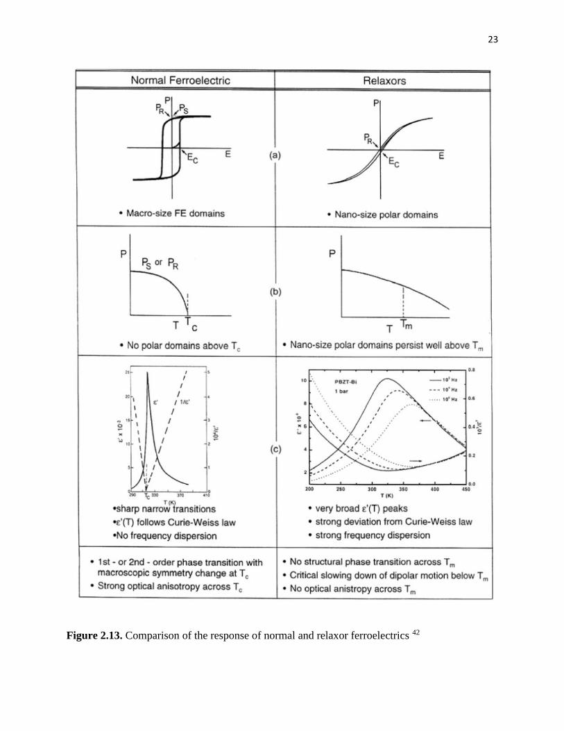
Figure 2.13. Comparison of the response of normal and relaxor ferroelectrics…………………23
Figure 2.14. Schematic of the movement of domain walls, indicated by the red dots, across a
complex energy landscape under subswitching AC electric fields………………………………25
Figure 2.15. Flexoelectric response in barium strontium titanate as a function of temperature
above the ferroelectric-paraelectric phase transition temperature, indicated by the line at
21°C...…………………………………………………………………………………………....27
Figure 2.16. A comparison of the measured and predicted flexocoupling, relating flexoelectric
coeffcient and the dielectric susceptablity, for barium strontium titanate ceramics………………28
Figure 3.1. Scanning electron micrograph of CSD films on silicon crystallized at 900°C……..36
Figure 3.2. Differences in lattice parameters for different substrates as a function of coefficient of
thermal expansion compared to BST……………………………………………………………..37
Figure 3.3. Scanning electron micrograph of Ba0.6Sr0.4TiO3 films deposited crystallized for one
minute at 900°C on MgO………………………………………………………………………...38
Figure 3.4. Scanning electron micrograph of the Ba0.7Sr0.3TiO3 thin films deposited onto platinized
MgO substrates, showing a dense film…………………………………………………………...39
xii
Figure 3.5. First set of pulsed laser deposited Ba0.7Sr0.3TiO3 thin films on platinized alumina
substrates deposited at 700°C with an energy density of 1.5 J/cm2 ……………………………….41
Figure 3.6. Pulsed laser deposition of Ba0.7Sr0.3TiO3 thin films on alumina substrates at 1.25
J/cm2……………………………………………………………………………………………...42
Figure 3.7. X-ray diffraction pattern for sputtered and CSD Ba0.7Sr0.3TiO3 thin films deposited on
Al2O3 MgO substrates respectively. Substrate and electrode peaks indicated by * and o…………46
Figure 3.8. Schematic of the polishing set up for BST PFM samples…………………………….52
Figure 4.1. Schematic of the e31,f (electric field, strain) metrology and sample…………….....57
Figure 4.2. Image of e31,f (Electric field and Strain) measurement system in operation………..58
Figure 4.3. Quarter Wheatstone bridge circuit used for dynamic strain measurements…………58
Figure 4.4. Schematic of the charge to voltage converter used in the charge portion of the
piezoelectric measurements……………………………………………………………………...59
Figure 4.5. A comparison of the transverse piezoelectric response, e31,f, as a function of applied
DC electric fields for BST films with varied compositions and substrates……………………...64
Figure 4.6. Tunability and DC electric field dependence of the dielectric loss tangent in BST
films with varied composition and substrate…………………………………………………….65
Figure 4.7. Normalized irreversible Rayleigh behavior for 70:30 BST on MgO and Si, and 60:40
BST on MgO thin films………………………………………………………………………….67
Figure 4.8. Schematic of the DC strain gauge measurement circuit…………………………….69
Figure 4.9. The impacts of strain on the electric field induced e31,f of BST 70:30 on Si……….70
xiii
Figure 5.1. Schematic of the dielectric response as a function of temperature through the
paraelectric to ferroelectric phase transition in barium strontium titanate………………………75
Figure 5.2. DC electric field dependence of the capacitance (symbols) and dielectric loss tangent
(thin lines), for CSD BaxSr1-xTiO3 thin films at room temperature and 100kHz………………….79
Figure 5.3. Tunability, DC field dependence of the capacitance (filled symbols) and dielectric
loss tangent (open symbols), for a sputtered Ba0.7Sr0.3TiO3 thin film on alumina………………80
Figure 5.4. Capacitance (filled symbols) and dielectric loss tangent (open symbols) as a function
of temperature from 1kHz to 1MHz for a sputtered Ba0.7Sr0.3TiO3 thin film………………...……82
Figure 5.5. Permittivity (filled symbols) and dielectric loss tangent (open symbols) as a function
of temperature from 100Hz to 1MHz for a CSD Ba0.7Sr0.3TiO3 thin film…………………..…….83
Figure 5.6. Characteristic capacitance (above) and dielectric loss tangent (below) small signal AC
electric field response for a sputtered Ba0.7Sr0.3TiO3 thin film measured through the temperature
range of the global phase transition determined by the dielectric temperature response at a
frequency of 1MHz (lines are added to guide the eye)……………………………………………85
Figure 5.7. Rayleigh response for a sputtered BST thin film on alumina substrates as a function
of temperature, Ba0.7Sr0.3TiO3 thin film as a function of temperature…………………………….86
Figure 5.8. Characteristic permittivity (above) and dielectric loss (below) as a function of AC
electric field response for a CSD Ba0.7Sr0.3TiO3 thin film with a global phase transition temperature
of -22°C at 100 kHz……………………………………………………………………………....87
Figure 5.9. A comparison of the irreversible Rayleigh response as a function of normalized
temperature for sputtered and CSD BaxSr1-xTiO3 thin films……………………………………...89
xiv
Figure 5.10. Polarization-electric field for the sputtered Ba0.7Sr0.3TiO3 thin film taken on
increasing voltage at room temperature and 100Hz………………………………………………90
Figure 5.11. Polarization electric field loops for the CSD Ba0.7Sr0.3TiO3 thin film taken at room
temperature. b.(inset) Magnification showing the remanent polarization and the coercive electric
field. P-E loops were extremely slim, indicating the materials were likely macroscopically
paraelectric at room temperature…………………………………………………………………91
Figure 5.12. Minor polarization-electric field loop for a sputtered Ba0.7Sr0.3TiO3 thin film taken at
room temperature and 100 Hz…………………………………………………………………….93
Figure 5.13. Frequency dependence of the capacitance as a function of applied small signal AC
electric field for a sputtered Ba0.7Sr0.3TiO3 thin film……………………………………………...94
Figure 5.14. Leakage current for the CSD and sputtered BST thin films……………………….95
Figure 6.1. Ba0.4Sr0.6TiO3 ceramics with different pre-calcination mixing times a. 0 hours, b. 3
hours, c. 6 hours, and d. 9 hours3. The amount of dielectric dispersion characteristic of relaxor
ferroelectric characteristics is larger for shorter mixing times…………………………………102
Figure 6.2. The dielectric temperature dependence of Ba0.8Sr0.2TiO3 chemical solution deposited
thin films on MgO showing a broad maximum and frequency dispersion……………………..104
Figure 6.3. The irreversible Rayleigh response of various BST materials normalized to
temperatures above the ferroelectric phase transition…………………………………………..105
Figure 6.4. Normalized SHG response from the 70:30 BST ceramic samples taken at a ramp rate
of 3 °C/min and 6 °C/min………………………………………………………………………107
xv
Figure 6.5. Normalized SHG response above the transition temperature in the 70:30 BST
ceramic samples taken at a ramp rate of 3 °C/min measured first on heating then on cooling. The
red lines are added as a guide to highlight the change in slope. ……………………………….108
Figure 6.6. Normalized SHG response for the CSD 70:30 BST thin films, with the temperature
of the maximum in the dielectric response indicated by the arrow for comparison……………110
Figure 6.7. Normalized SHG response for the sputtered 70:30 BST thin films, with the
temperature of the maximum in the dielectric response indicated by the arrow for
comparison……………………………………………………………………………………...111
Figure 6.8. Transmission electron microscopy and electron energy loss spectroscopy of 70:30
BST ceramics……………………………………………………………...................................113
Figure 6.9. Transmission electron microscopy and electron energy loss spectroscopy of
sputtered 70:30 BST thin films…………………………………………………………………114
Figure 7.1. Schematic of the flexoelectric testing system and flexoelectric response…………121
Figure 7.2. Temperature dependence of the Rayleigh response and flexoelectric coefficient (Ma
and Cross), normalized to the ferroelectric-paraelectric phase transition temperature………...123
Figure 7.3. Impact of applied strain gradient on the coercive field of a flexoelectric sample
showing flexo-poling and residual imprint upon removal of the electric field…………………126
Figure 7.4. The polarization as a function of applied strain gradient in lead zirconate
titanate..........................................................................................................................................127
xvi
Figure 7.5. Hysteresis in polarization with increasing and decreasing applied strain gradient and
the development of a piezoelectric response. The d33 measurements were taken after the strain
gradient was removed, and hence are remanent piezoelectric coefficients………………….....128
Figure 8.1. Image of the PZT films after wire bonding to the top and bottom electrodes……..140
Figure 8.2. Leakage current as a function of time for a randomly oriented, 1µm thick, chemical
solution deposited Pb(Zr0.52Ti0.48)O3 thin film taken at 150 kV/cm and 180 °C……………….142
Figure 8.3. The time to failure for data sets at three temperatures from a CSD PZT thin film..143
Figure 8.4. Median time to failure PZT thin films deposited by different methods, as a function
of temperature at a constant voltage. While the chemical solution deposited films were tested at
150 kV/cm, the short lifetimes of the sputtered films required a reduction in the field to 100
kV/cm…………………………………………………………………………………………...145
Figure 8.5. Median time to failure as a function of voltage at constant temperature of 150 °C for
PZT thin films…………………………………………………………………………………..146
Figure 8.6. Fitting of the leakage current-voltage measurements over a range of temperature for
CSD PZT thin films……………………………………………………………………………..149
Figure 8.7. Refitting the highly accelerated lifetime testing for Pb(Zr,Ti)O3 thin films deposited
by different methods with different crystallographic orientations. The predicted voltage
acceleration factor for the refit data is -2, which is in good agreement with the refit slopes……..151
Figure 8.8. Voltage contrast microscopy of PZT thin film devices under 30 V for 4.5 hours
showing regions of resistance degradation……………………………………………………..154
xvii
Figure 8.9. Scanning electron micrograph of an area of ejected material after electrical testing in
a PZT thin film………………………………………………………………………………….155
Figure 9.1. Characteristic EDS response from barium titanate………………………………...165
xviii
LIST OF TABLES
Table 3.1. Pulsed Laser Deposition of BST Films………………………………………………41
Table 3.2. Sputter Processing Conditions……………………………………………………….43
Table 3.3. Lattice parameters and lattice volumes calculated from X-ray diffraction in figure
3.7………………………………………………………………………………………………...47
Table 4.1 Calibration of the e31,f (Electric Field and Strain) Measurement System………………61
Table 4.2. Transition temperature, tunability, dielectric loss and Rayleigh behavior for BST films
at 100kHz………………………………………………………………………………………...62
Table 5.1. Relative tunability and minimum quality factor at maximum tunability calculated for
the CSD Ba1-xSrxTiO3 thin films at 100kHz………………………………………………………79
Table 8.1. Compilation of previous literature on reliability in PZT thin films………………...138
Table 8.2. Median time to failure and Weibull fitting parameter for each temperature data
set……………………………………………………………………………………………….144
Table 8.3. Previous studies on mechanisms associated with a given activation energy in
PZT…………………………………………………………………………………………......145
Table 8.4. Activation energy and voltage acceleration factor determined from the Eyring model
and the voltage acceleration calculated from the new model……………………………………152
Table 8.5. List of conduction mechanisms in dielectrics………………………………………..148
Table 9.1. Flexoelectric and flexocoupling response in a series of perovskite materials………..163
xix
ACKNOWLEDGEMENTS
I am truly grateful to have so many good people in my life who have taught me so much. I
would first like to thank my advisor Dr. Trolier-McKinstry for taking me on as a student. She has
taught me, what I expect to be, some of the most important lessons on life and science. Her
intensity and compassion inspire me. I would also like to thank the members of my committee,
Drs. Randall, Lanagan, and Jackson for their guidance. Additionally, I would like to thank Dr.
Meyer for always being supportive. I would like to acknowledge the MCL staff, particularly Jeff
and Tim, who have given so much of their time.
I would also like to thank the many members of the STM, Messing, Randall, Maria,
Gopalan, and Meyer groups who have helped me over the years. A special thanks to Raegan,
Derek, Nevin, and Susie who have helped me immensely both scientifically and personally. And
to those from Missouri for never letting me forget where I come from.
And most importantly, I am grateful for the love and support of my family and Casey
Newell. Without your love and support I would not have thought my dreams possible.
1
Chapter 1.
Thesis Overview
This section provides a brief introduction to the research discussed within this thesis in
order to provide a framework for the project objectives. After presenting the project objectives, a
short section is provided on the thesis organization.
1.1 Introduction
As telecommunication frequency standards become increasingly complex and devices
more compact, it becomes necessary to develop efficient tunable systems.1 Thin film tunable
dielectrics enable cost-effective and scalable frequency agile technologies.2, 3 Barium strontium
titanate, BST, thin film tunable dielectrics offer high tunability, but suffer from comparatively high
dielectric loss in the microwave region.2,4,5 Because of this, BST based devices have to-date been
limited.4 The communication quality factor, a figure of merit for frequency agile systems,
highlights the importance of balancing tunability and dielectric loss and is given by:
= ( − 1)∙ (0) ∙ ( )where η is the tunability and tanδ(0) and tanδ(E) are the unbiased and biased dielectric loss.4 Thus,
developing efficient BST based tunable systems is dependent on an understanding of and, where
possible, mitigation of, the factors impacting dielectric loss.
2
Losses are incurred in BST thin films through several intrinsic and extrinsic mechanisms.
In addition to intrinsic phonon-based loss mechanisms, residual ferroelectricity, electric field
induced piezoelectricity and electrical degradation have been observed to contribute to the
dielectric loss in BST thin films.6,7,8,9 Intrinsic loss and residual ferroelectric contributions to
dielectric loss occur in unbiased materials. Mechanisms such as electric field-induced
piezoelectricity and electrical degradation are dependent upon the application of an electric field
and cannot be completely circumvented. However, with an understanding of the material response,
the contributions to loss from induced piezoelectricity can be minimized through design
optimization. Similarly, by understanding the mechanisms of breakdown under electrical
degradation, predictions of the material reliability can be made. Thus providing an understanding
of loss in tunable dielectrics is the first step towards the development of lower loss, higher
tunability frequency agile systems. In addition to the benefits to tunable dielectrics, understanding
and mitigating loss in barium strontium titanate-based materials impacts a broad range of
applications, including dielectric electrostatic energy storage.10
1.2 Thesis Objectives
The overall goal of this work is to characterize loss mechanisms in barium strontium
titanate thin films for tunable dielectric applications. This work focuses on the ferroelectric,
piezoelectric and dielectric contributions to dielectric loss experienced during tuning. Rayleigh
analysis is employed to investigate the ferroelectric response as a function of temperature near and
above the paraelectric phase transition. This methodology provides information on ferroelectric
contributions to dielectric loss (and the flexoelectric response) in the paraelectric phase. Electric
3
field-induced piezoelectricity is also characterized, and a discussion of the development and
calibration of the piezoelectric metrology tool is included to provide context. Additional
background information is provide on the specific methodologies and metrologies employed
within this study, including; e31,f piezoelectric response as a function of electric field and strain,
second harmonic generation, transmission electron microscopy and flexoelectric poling.
1.3 Thesis Organization
The second chapter is dedicated to a discussion of the relevant background literature on the
essential phenomenology and material properties of barium strontium titanate thin films. Chapter
three includes the thin film processing and the physical and electrical thin film characterization.
The fourth chapter discusses the design, calibration and development of the e31,f(electric field and
strain) piezoelectricity metrology and the DC electric field-induced piezoelectric response in a
series of BST thin films. The next section, chapter five, covers measurements of the residual
ferroelectricity contributions to dielectric loss through Rayleigh analysis and the corroborating
electrical characterization. Chapter five also includes a discussion of the possible underlying
mechanisms leading to the development of residual ferroelectricity in BST thin films. Chapter 6
begins a discussion on the impact of residual ferroelectricity on flexoelectric response in BST
ceramics. Chapter 7 consists of the work on conduction mechanisms, reliability and breakdown in
piezoelectric thin films. And chapter 8 includes possible future work which stems from the
observations made during this study.
4
1.4 References
1. Yang, L., Hou, W., Cao, L., Zhao, B. Y. & Zheng, H. Supporting Demanding Wireless Applications
with Frequency-agile Radios. in Proc. 7th USENIX Conf. Networked Syst. Des. Implement. 5–5
(USENIX Association, 2010).
2. Tiggelman, M. P. J., Reimann, K., Van Rijs, F., Schmitz, J. & Hueting, R. J. E. On the Trade-Off
Between Quality Factor and Tuning Ratio in Tunable High-Frequency Capacitors. IEEE Trans.
Electron Devices 56, 2128–2136 (2009).
3. Bao, P., Jackson, T. J., Wang, X. & Lancaster, M. J. Barium strontium titanate thin film varactors for
room-temperature microwave device applications. J. Phys. Appl. Phys. 41, 063001 (2008).
4. Tagantsev, A. K., Sherman, V. O., Astafiev, K. F., Venkatesh, J. & Setter, N. Ferroelectric Materials
for Microwave Tunable Applications. J. Electroceramics 11, 5–66 (2003).
5. York, R. A. Tunable Dielectrics for RF Circuits, in Multifunctional Adaptive Microwave
Circuits and Systems, Scitech Pub., 2009, ch. 4.
6. Gurevich, V. L. & Tagantsev, A. K. Intrinsic dielectric loss in crystals. Adv. Phys. 40, 719–767 (1991).
7. Garten, L. M., Lam, P., Harris, D., Maria, J.-P. & Trolier-McKinstry, S. Residual ferroelectricity in
barium strontium titanate thin film tunable dielectrics. J. Appl. Phys. 116, 044104 (2014).
8. Noeth, A., Yamada, T., Tagantsev, A. K. & Setter, N. Electrical tuning of dc bias induced acoustic
resonances in paraelectric thin films. J. Appl. Phys. 104, 094102 (2008).
9. Zafar, S., Jones, R., Jiang, B., White, B., Kaushik, V., Gillespie, S. The electronic conduction
mechanism in barium strontium titanate thin films. Appl. Phys. Lett. 73, 3533–3535 (1998).
10.Roy, D. & Krupanidhi, S. B. Excimer laser ablated barium strontium titanate thin films for dynamic
random access memory applications. Appl. Phys. Lett. 62, 1056–1058 (1993).
5
Chapter 2
Background Literature
2.1 Barium Strontium Titanate
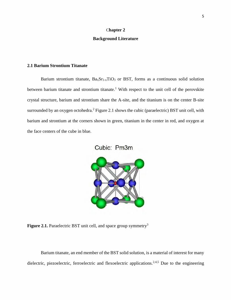
Barium strontium titanate, BaxSr1-xTiO3 or BST, forms as a continuous solid solution
between barium titanate and strontium titanate.1 With respect to the unit cell of the perovskite
crystal structure, barium and strontium share the A-site, and the titanium is on the center B-site
surrounded by an oxygen octohedra.2 Figure 2.1 shows the cubic (paraelectric) BST unit cell, with
barium and strontium at the corners shown in green, titanium in the center in red, and oxygen at
the face centers of the cube in blue.
Figure 2.1. Paraelectric BST unit cell, and space group symmetry3
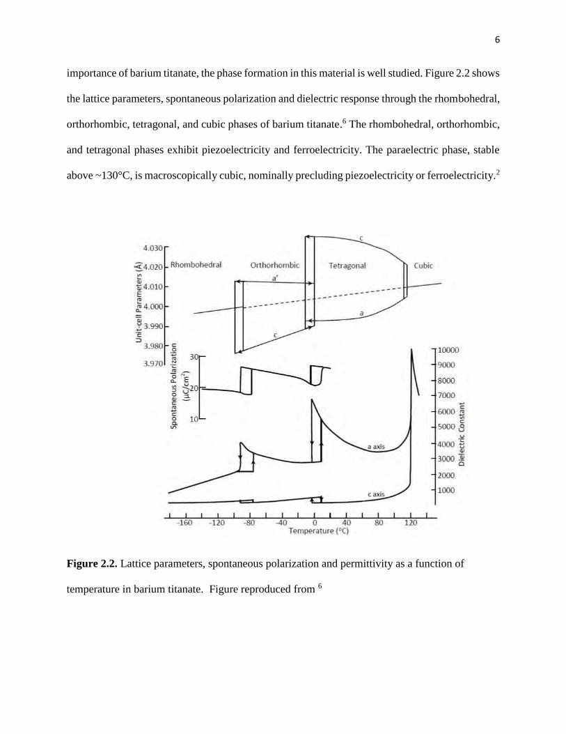
Barium titanate, an end member of the BST solid solution, is a material of interest for many
dielectric, piezoelectric, ferroelectric and flexoelectric applications.2,4,5 Due to the engineering
6
importance of barium titanate, the phase formation in this material is well studied. Figure 2.2 shows
the lattice parameters, spontaneous polarization and dielectric response through the rhombohedral,
orthorhombic, tetragonal, and cubic phases of barium titanate.6 The rhombohedral, orthorhombic,
and tetragonal phases exhibit piezoelectricity and ferroelectricity. The paraelectric phase, stable
above ~130°C, is macroscopically cubic, nominally precluding piezoelectricity or ferroelectricity.2
Figure 2.2. Lattice parameters, spontaneous polarization and permittivity as a function of
temperature in barium titanate. Figure reproduced from 6
7
In BaTiO3 and barium strontium titanate, the paraelectric to ferroelectric transition has
characteristics of both a displacive and order-disorder type phase transition as first observed by
Comes.7,8,9 Displacive phase transitions are characterized by the displacement of an atom (or
atoms) with respect to neighboring atoms in a unit cell, where the displacements are generally
small with respect to the size of the unit cell.10 In BaTiO3-based materials, the displacive phase
transition is attributed to the condensation of the transverse optic phonon mode, or soft mode, at
the Brillouin zone center.10 This model accounts for the observed phonon spectrum and the Curie
constant of the first order, displacive ferroelectric phase transition.2 In BaTiO3, the displacement
refers to the offsetting of the titanium from the center of unit cell towards an oxygen on one of the
face-centers, with correlated motion of the oxygen sublattice.2,11 The resulting unit cell is
tetragonal, with one unique lattice parameter and three orthogonal axes. Within the tetragonal unit
cell, the centers of positive and negative charge are no longer coincident, breaking the center of
symmetry and creating a dipole.
Barium titanate based materials have some characteristics which are consistent with order-
disorder type phase transitions.7,12,13 The ordering in this instance refers to the coalescence of local
titanium displacements along the <111>, as shown in Figure 2.3. These local structural
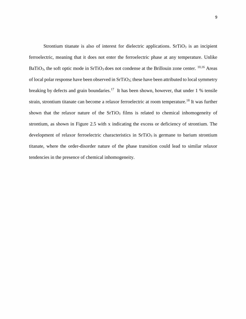
displacements have been observed ~100 °C above the displacive phase transition temperature, as
shown in the birefringence and Raman data for barium titanate single crystals in Figure 2.4.13 X-
ray absorption fine structure analysis shows the titanium displacements occurring along [111]
direction, but nuclear magnetic resonances, NMR, indicates a more tetragonal-like symmetry,
which would consistent with a time averaged symmetry.9 An eight site (rhombohedrally
displaced) local structure in paraelectric BST is further supported by neutron diffraction, XAFS,
and diffuse scattering distributions.14 It has also been suggested that the dynamic rhombohedral
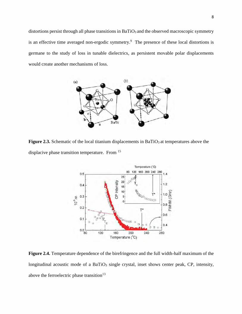
8
distortions persist through all phase transitions in BaTiO3 and the observed macroscopic symmetry
is an effective time averaged non-ergodic symmetry.9 The presence of these local distortions is
germane to the study of loss in tunable dielectrics, as persistent movable polar displacements
would create another mechanisms of loss.
Figure 2.3. Schematic of the local titanium displacements in BaTiO3 at temperatures above the
displacive phase transition temperature. From 15
Figure 2.4. Temperature dependence of the birefringence and the full width-half maximum of the
longitudinal acoustic mode of a BaTiO3 single crystal, inset shows center peak, CP, intensity,
above the ferroelectric phase transition13
9
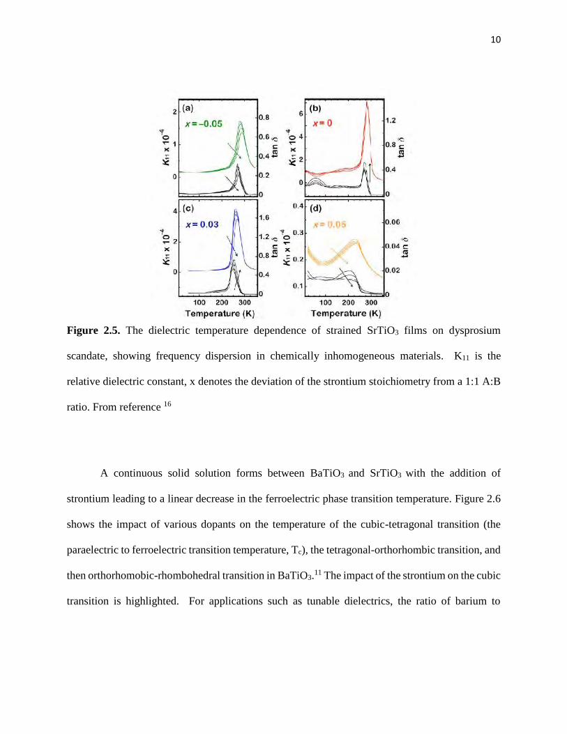
Strontium titanate is also of interest for dielectric applications. SrTiO3 is an incipient
ferroelectric, meaning that it does not enter the ferroelectric phase at any temperature. Unlike
BaTiO3, the soft optic mode in SrTiO3 does not condense at the Brillouin zone center. 10,16 Areas
of local polar response have been observed in SrTiO3; these have been attributed to local symmetry
breaking by defects and grain boundaries.17 It has been shown, however, that under 1 % tensile
strain, strontium titanate can become a relaxor ferroelectric at room temperature.18 It was further
shown that the relaxor nature of the SrTiO3 films is related to chemical inhomogeneity of
strontium, as shown in Figure 2.5 with x indicating the excess or deficiency of strontium. The
development of relaxor ferroelectric characteristics in SrTiO3 is germane to barium strontium
titanate, where the order-disorder nature of the phase transition could lead to similar relaxor
tendencies in the presence of chemical inhomogeneity.
10
Figure 2.5. The dielectric temperature dependence of strained SrTiO3 films on dysprosium
scandate, showing frequency dispersion in chemically inhomogeneous materials. K11 is the
relative dielectric constant, x denotes the deviation of the strontium stoichiometry from a 1:1 A:B
ratio. From reference 16
A continuous solid solution forms between BaTiO3 and SrTiO3 with the addition of
strontium leading to a linear decrease in the ferroelectric phase transition temperature. Figure 2.6
shows the impact of various dopants on the temperature of the cubic-tetragonal transition (the
paraelectric to ferroelectric transition temperature, Tc), the tetragonal-orthorhombic transition, and
then orthorhomobic-rhombohedral transition in BaTiO3.11 The impact of the strontium on the cubic
transition is highlighted. For applications such as tunable dielectrics, the ratio of barium to
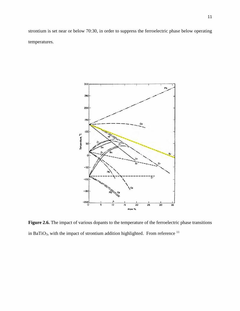
11
strontium is set near or below 70:30, in order to suppress the ferroelectric phase below operating
temperatures.
Figure 2.6. The impact of various dopants to the temperature of the ferroelectric phase transitions
in BaTiO3, with the impact of strontium addition highlighted. From reference 11
12
2.2. Frequency Agile Systems
Barium strontium titanate thin films are of interest for tunable dielectrics in frequency agile
applications. This section covers the motivation behind the development of frequency agile
electronics with a particular focus on tunable dielectrics.
Frequency agile electronics allow for the optimization of the telecommunication frequency
space, while minimizing the electronics footprint. Due to the limitations of wideband circuitry and
analogue-to-digital converters, the development of tunable radio frequency front ends is critical
for multi-frequency telecommunications.19 Frequency agile technologies are currently being
developed for military and commercial telecommunications applications.19,20 Frequency switching
is often used in tactical military communications to prevent tracking or jamming of battlefield
communications.21
Practical implementation of any frequency agile technology requires a combination of high
tunability and low loss. The communication quality factor, K, is a figure of merit for frequency
agile systems which highlights the importance of balancing tunability and loss.22 The
communication quality factor is calculated as follows:
= ( − 1)× (0) × ( )where η is the tunability, and tanδ(0) and tanδ(E) are the dielectric loss at zero field and at the
electric field, E, used for tuning.
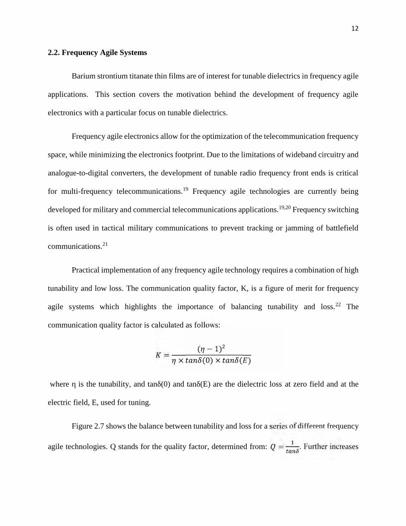
Figure 2.7 shows the balance between tunability and loss for a series of different frequency
agile technologies. Q stands for the quality factor, determined from: = . Further increases
13
in quality factor, and thus decreases in loss, would facilitate the competitiveness of tunable
dielectrics as a viable frequency agile technology.
Figure 2.7. A comparison of quality factor and tunability for different tunable technologies 23
2.2.1. Tunable Dielectrics
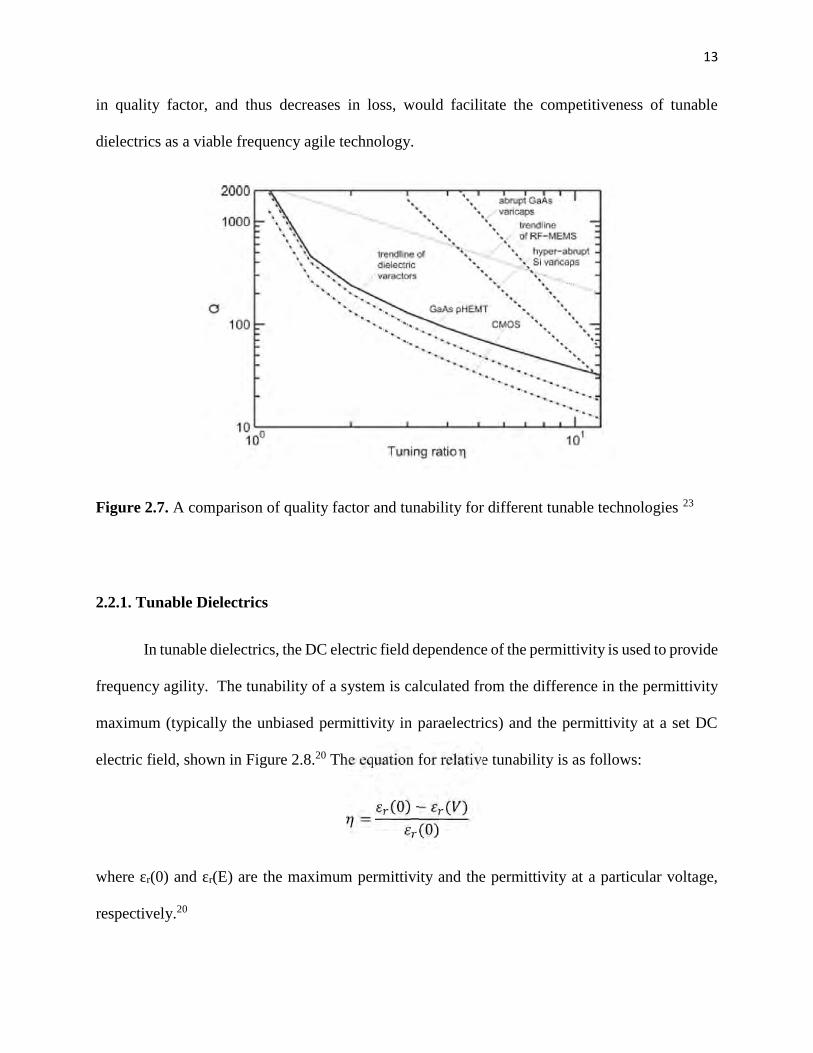
In tunable dielectrics, the DC electric field dependence of the permittivity is used to provide
frequency agility. The tunability of a system is calculated from the difference in the permittivity
maximum (typically the unbiased permittivity in paraelectrics) and the permittivity at a set DC
electric field, shown in Figure 2.8.20 The equation for relative tunability is as follows:
= (0) − ( )(0)where εr(0) and εr(E) are the maximum permittivity and the permittivity at a particular voltage,
respectively.20
14
Figure 2.8. The schematic of the dielectric voltage dependence from which the tuanbility can be
calculated20
Tunable dielectrics are based on solid state devices and as such, offer reliable, fast acting
tunability.19,20 Compared to tunable dielectrics, mechanically tunable filters tend to be slower and
larger, while varactor diodes are faster but have poor power handling and high losses in the RF.23
Tunable dielectrics are employed in voltage-controlled oscillators, tunable filters and phase
shifters.12,19,20,21 Barium strontium titanate is a primary candidate for tunable dielectrics. It offers
high tunability, fast tuning and high electric fields to breakdown,20 but still suffers from
comparatively high loss in the microwave region.22 In order to develop BST thin films as a
competitive tunable technology, the factors impacting loss need to be assessed and mitigated where
possible.
15
2.3. Dielectric Response
As the focus of this work is towards the development of barium strontium titanate in
dielectric applications, the next section will provide a brief discussion of the relevant terms
relating to the dielectric response.
2.3.1. Relative Permittivity
The relative permittivity is a measure of the polarizablity of a material compared to the
polarizability of free space. The equations for relative permittivity and the complex form of
relative permittivity in a capacitor are as follows:
= + =∗ = −
where D is the electric displacement vector, E is the applied electric field, P is the polarization, εo
is the permittivity of free space, and is the real and is the imaginary components of relative
permittivity.24,25 Contributions to relative permittivity arise from electronic (distortions of the
electron cloud), atomic (distortions in bond length between ions of different charge), dipole
orientation (the alignment of a permanent dipoles), hopping (movement of charges between
crystallographic sites) and space charge (macroscopic movement of charges until blocked by an
insulating interface) mechanisms.26 There is a frequency limit to the contribution from each source,
where loss of any contribution is associated with a relaxation or resonance. Figure 2.9 shows the
polarization which develops due to each mechanism as a function of the average response time.26
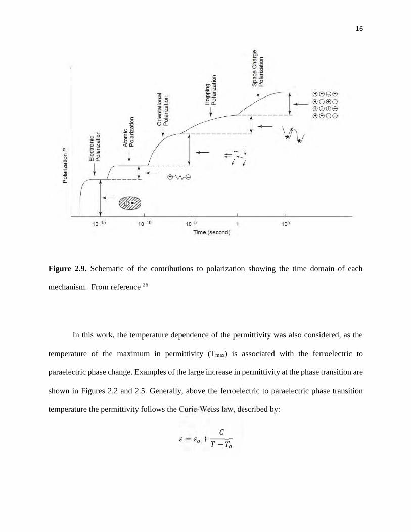
16
Figure 2.9. Schematic of the contributions to polarization showing the time domain of each
mechanism. From reference 26
In this work, the temperature dependence of the permittivity was also considered, as the
temperature of the maximum in permittivity (Tmax) is associated with the ferroelectric to
paraelectric phase change. Examples of the large increase in permittivity at the phase transition are
shown in Figures 2.2 and 2.5. Generally, above the ferroelectric to paraelectric phase transition
temperature the permittivity follows the Curie-Weiss law, described by:
= + −
17
where C is the Curie constant, and To is the Curie-Weiss temperature. In materials with first order
phase transitions, such as barium strontium titanate, the Curie-Weiss temperature and the transition
temperature Tc need not coincide.
2.3.2 Dielectric Loss
The figure of merit often used to gauge dielectric loss, which is measured as the ratio of
the imaginary to real permittivity, or the loss current to charging current, is the loss tangent, tanδ.24
High losses in the microwave regime make ferroelectric materials with domain wall contributions
to the loss, less interesting for microwave devices.27 Jin et al. have reported an extrinsic
(ferroelectric) contribution to the dielectric response and loss in perovskite ferroelectric ceramics
extending into the low gigahertz frequency range, producing both a strong dispersion and an
increase in dielectric loss in the frequency range of interest for tunable devices.28
The measured dielectric loss of a capacitor is a combination of intrinsic and extrinsic loss
mechanisms. Intrinsic loss in centrosymmetric materials comes from the three quantum and four
quantum loss mechanisms and in non-centrosymmetric materials, or materials under asymmetric
external stimuli, quasi-Debye loss mechanisms are also possible.29 Further external losses can
come from charged defects, hysteretic domain wall, cluster or phase boundary movements,
piezoelectric resonances, resistance degradation, and grain boundaries.30 It is these external loss
mechanisms that are the focus of this work.
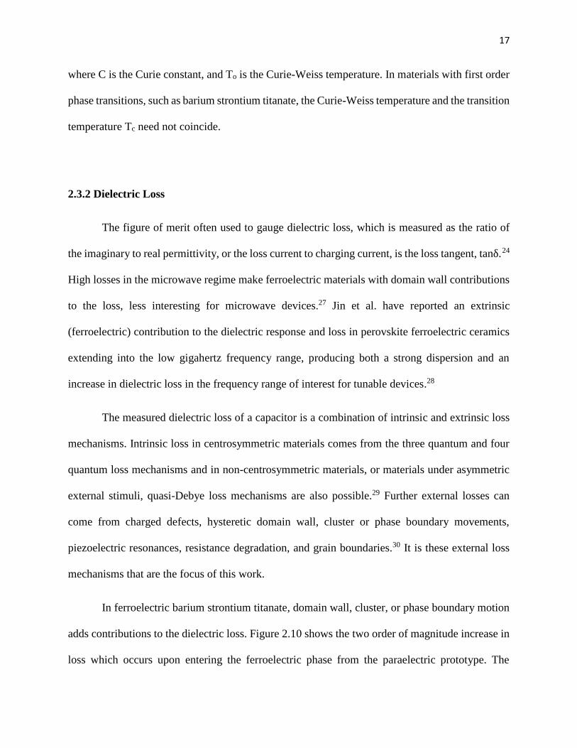
In ferroelectric barium strontium titanate, domain wall, cluster, or phase boundary motion
adds contributions to the dielectric loss. Figure 2.10 shows the two order of magnitude increase in
loss which occurs upon entering the ferroelectric phase from the paraelectric prototype. The
18
temperature of this onset is a function of the composition x in BaxSr1-xTiO3. In the ferroelectric
phase, the material is also piezoelectric, leading to addition loss mechanisms discussed in the next
section. In this work, the impact of residual ferroelectricity –a persistent ferroelectric response
above the global ferroelectric temperature, and DC electric field induced piezoelectric loss
mechanisms are characterized.
Figure 2.10. Dielectric loss tangent as a function of temperature for different compositions of
BaxSr1-xTiO3. From reference 31
2.4. Piezoelectricity
The direct piezoelectric effect is the linear coupling between mechanical stress and electric
polarization.11 The coefficients of the direct response are equivalent to those of the converse
19
piezoelectric response, which relates the applied electric field to mechanical strain.32 The equations
for the direct and converse piezoelectric effect are as follows:
== −
where D is the dielectric displacement, E is the applied electric field, x is the strain and e is the
piezoelectric coefficient.25 Piezoelectricity is a third order tensor properties and thus exclusive to
materials lacking a center of symmetry or other combinations of symmetry elements that forbid
the effect (e.g. as for point group 432 and the Curie group symmetry in unpoled ferroelectrics).
Often for thin film applications, the piezoelectric response of interest is the e31,f coefficient, which
relates the in-plane strain to the out of plane dielectric displacement.33
2.4.1. DC Electric Field Induced Piezoelectricity
In tunable dielectrics, induced piezoelectricity is one mechanism leading to increased loss.
Intrinsic piezoelectricity is exclusive to materials for which the third rank tensor property is not
symmetry-forbidden. However, the application of an electric field to a centrosymmetric material
can induce piezoelectricity through a distortion of structure along the direction of the electric
field.34 In tunable dielectrics, induced piezoelectricity is a consequence of the DC electric fields
used for tuning. Induced piezoelectricity leads to resonances in impedance, shown in Figure 2.9,
which interfere with impedance matching.,35,36
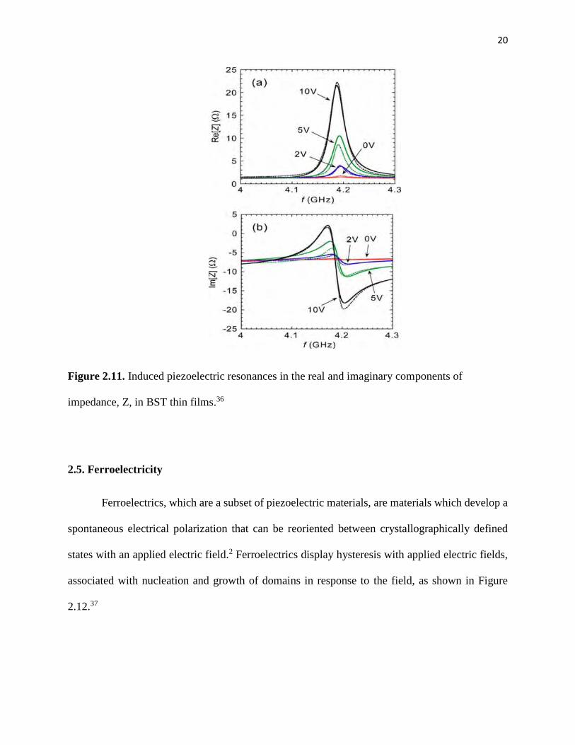
20
Figure 2.11. Induced piezoelectric resonances in the real and imaginary components of
impedance, Z, in BST thin films.36
2.5. Ferroelectricity
Ferroelectrics, which are a subset of piezoelectric materials, are materials which develop a
spontaneous electrical polarization that can be reoriented between crystallographically defined
states with an applied electric field.2 Ferroelectrics display hysteresis with applied electric fields,
associated with nucleation and growth of domains in response to the field, as shown in Figure
2.12.37
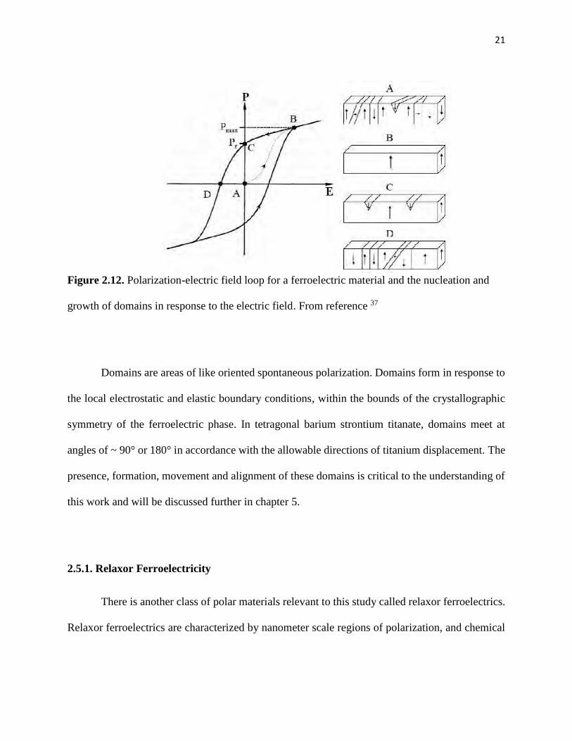
21
Figure 2.12. Polarization-electric field loop for a ferroelectric material and the nucleation and
growth of domains in response to the electric field. From reference 37
Domains are areas of like oriented spontaneous polarization. Domains form in response to
the local electrostatic and elastic boundary conditions, within the bounds of the crystallographic
symmetry of the ferroelectric phase. In tetragonal barium strontium titanate, domains meet at
angles of ~ 90° or 180° in accordance with the allowable directions of titanium displacement. The
presence, formation, movement and alignment of these domains is critical to the understanding of
this work and will be discussed further in chapter 5.
2.5.1. Relaxor Ferroelectricity
There is another class of polar materials relevant to this study called relaxor ferroelectrics.
Relaxor ferroelectrics are characterized by nanometer scale regions of polarization, and chemical
22
inhomogeneity at similar length scales.38,39 Chemical ordering has been shown in some materials,
such as Pb(Sc0.5Ta0.5)O3, to lead to a transition from relaxor to normal ferroelectric behavior. 40,41
Relaxor ferroelectrics do not go exhibit the sharp phase transition observed in normal
ferroelectrics. Rather nano-scale polar regions persist up to the Burns temperature, which can be
over 100°C above Tmax. Macroscopic manifestations of relaxor behavior include a characteristic
frequency dispersion and diffuse maximum observed in the dielectric temperature response.
Additionally, the polarization-electric field hysteresis loops in relaxor ferroelectrics are
characteristically very thin. Figure 2.13 shows a comparison of dielectric and ferroelectric
properties of normal and relaxor ferroelectrics.42 Figure 2.13 shows a gradual decay in the
polarization which is very different than the response expected for a first-order or second-order
phase transition. This gradual decay in the polarization is attributed to the persistence of the nano-
scale polar regions to higher temperatures. Figure 2.5 also provides an example of relaxor
ferroelectric behavior in a non-stoichiometric strontium titanate thin film, an end member of
barium strontium titanate.
23
Figure 2.13. Comparison of the response of normal and relaxor ferroelectrics 42
24
2.5.2. Rayleigh analysis
Rayleigh analysis, first developed to describe the non-linear response of the magnetization to
the applied magnetic field,43 has been adapted to describe the field dependence of the dielectric
and piezoelectric response in ferroelectric materials.44,45 The amplitude dependence of the
dielectric response is coupled to a hysteresis attributed to the interaction of domain walls, phase
boundaries or domain wall clusters with pinning centers in the material.46 The Rayleigh
relationship for dielectric non-linearity is given by:
= +where is the reversible and irreversible Rayleigh coefficient, and EAC is the oscillating
electric field.44 Rayleigh analysis is conducted within the subswitching regime, typically EAC <
half the coercive electric field, in order to avoid changes in the domain structure.47 Reversible
contributions to the dielectric response arise from the intrinsic lattice response and non-lossy
domain wall motion; irreversible contributions come from the pinning and depinning of domains
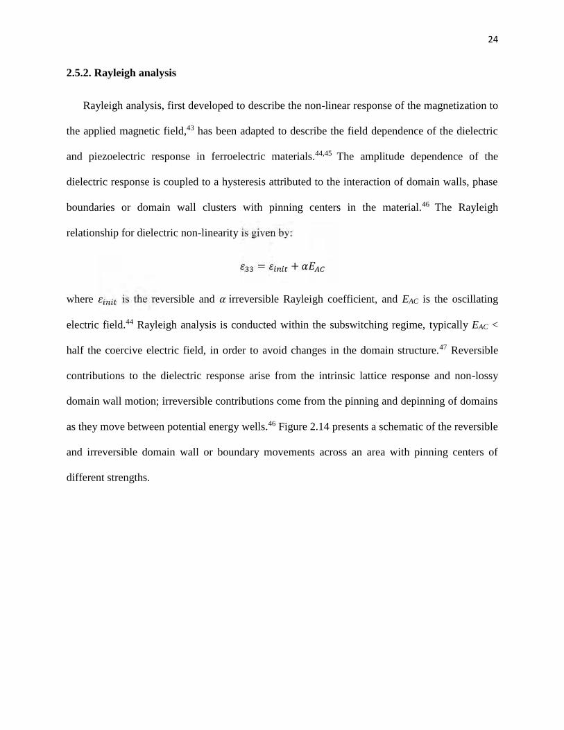
as they move between potential energy wells.46 Figure 2.14 presents a schematic of the reversible
and irreversible domain wall or boundary movements across an area with pinning centers of
different strengths.
25
Figure 2.14. Schematic of the movement of domain walls, indicated by the red dots, across a
complex energy landscape under subswitching AC electric fields48
2.6. Flexoelectricity
Flexoelectricity describes the development of polarization due to the application of a
strain gradient.5 The equations for flexoelectricity are:
= +where P is the polarization, is the dielectric susceptibility, E is the electric field, µ is the
flexoelectric coefficient, and ∂u/∂x is the strain gradient.49 Flexoelectricity is an even rank tensor
property, and as such can occur in a material of any symmetry. For a material with macroscopic
cubic symmetry, such as paraelectric or unpoled ferroelectric barium strontium titanate, the
26
allowable property matrix includes the µ1111, µ1122, and the µ1212 coefficients (µ11, µ12, and µ44 in
matrix notation).50
Flexoelectricity was first predicted by Mashkevich and Tolpygo, with the phenomenology
developed by Kogan and adapted by Indembon, Longinov and Osipov.51 Early estimates of the
flexoelectric coefficients in simple solids predicted a response of approximately 10-10-10-11 C/m.
50,51 Four decades later, Ma and Cross discovered flexoelectric coefficients in lead magnesium
niobate over 5 µC/m.50 These flexoelectric measurements were made on clamped cantilever
samples with 1 Hz excitation strain, with strain measured via differential variable reluctance
transducers which were phase locked to the charge output from the sample.52 The alignment of
nano-polar regions, associated with relaxor ferroelectricity, due to strain-gradient poling was
proposed as the justification for the enhancements in flexoelectric response.50 However
investigations of materials with a similar structure but (theoretically) lacking nanopolar regions,
such as barium strontium titanate, showed an increase in the µ12 flexoelectric coefficient to over
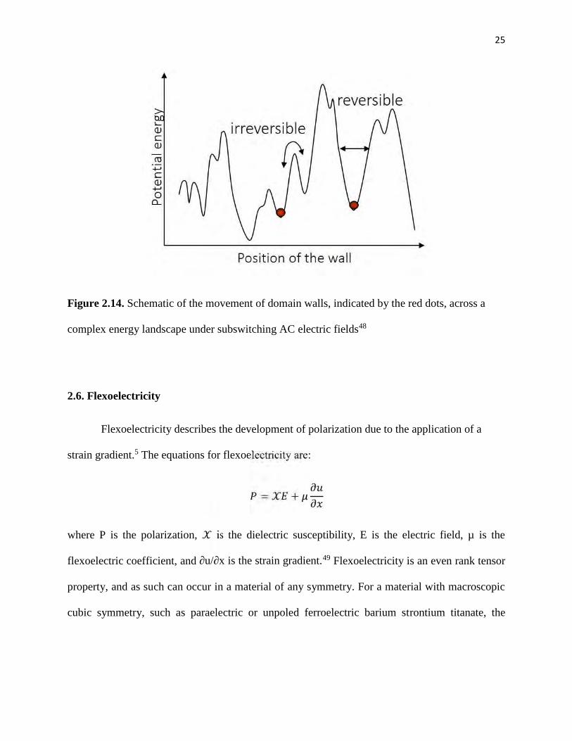
100 µC/m within 2°C of the transition temperature.52 The temperature dependent flexoelectric
results for BST are shown in Figure 2.15.52
27
Figure 2.15. Flexoelectric response in barium strontium titanate as a function of temperature
above the ferroelectric-paraelectric phase transition temperature, indicated by the line at 21°C.51
The increase in flexoelectric response six orders of magnitude above theoretical predictions
was unexpected, and required revisiting the flexoelectric phenomenology for high permittivity
dielectrics. Tagantsev proposed a relationship between the polarizability of the material and the
polarization which develops due to an applied strain gradient.52,53 The relationships between
dielectric susceptibility, , and flexoelectric coefficient, µ, are as follows:
=≈ 4 ≅ 1 − 10
where f is the flexocoupling coefficient, q is the charge on an electron, and a is the lattice
parameter. Flexocoupling is expected to be within 1-10 volts for most materials. Flexocoupling
28
coefficients for perovskite materials predict the destabilization of the perovskite structure into an
incommensurate phase for flexocoupling factors greater than 10 volts.49,54 However, there have
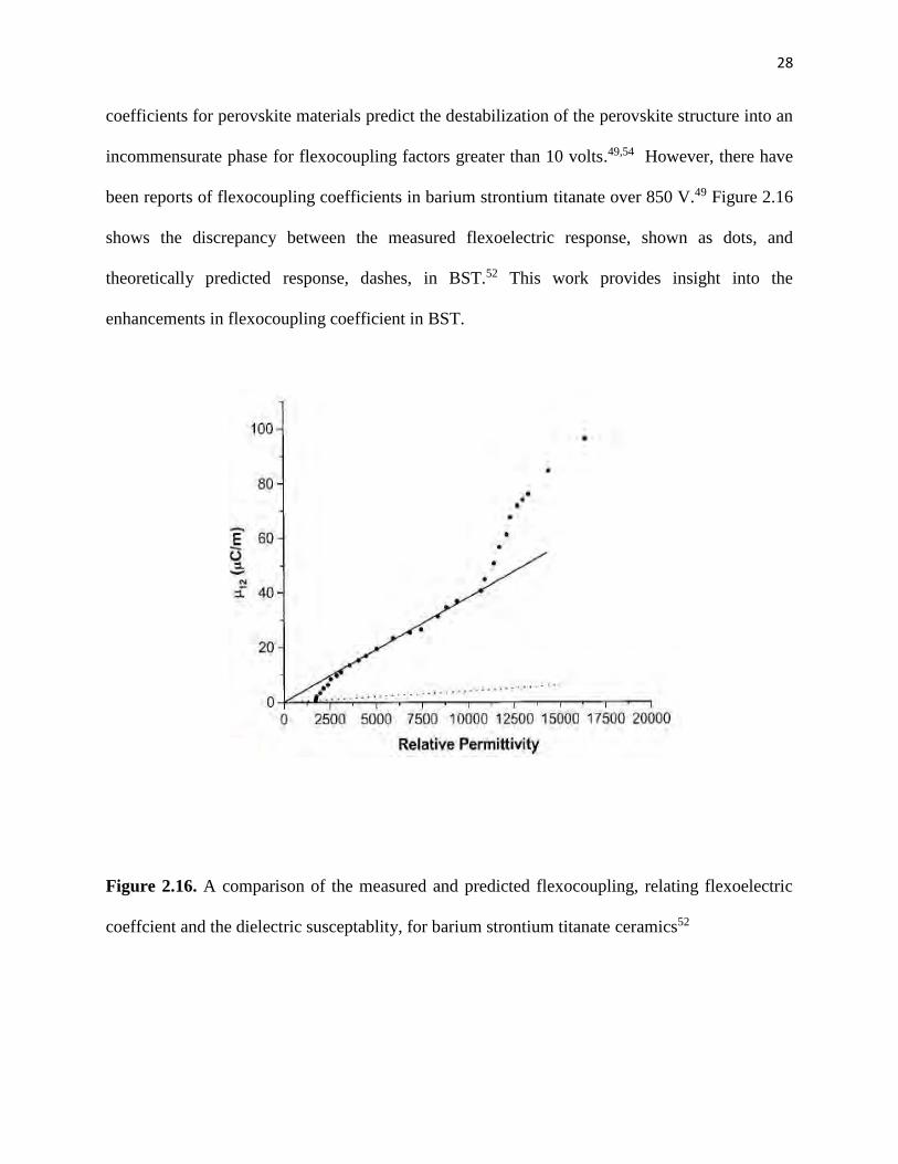
been reports of flexocoupling coefficients in barium strontium titanate over 850 V.49 Figure 2.16
shows the discrepancy between the measured flexoelectric response, shown as dots, and
theoretically predicted response, dashes, in BST.52 This work provides insight into the
enhancements in flexocoupling coefficient in BST.
Figure 2.16. A comparison of the measured and predicted flexocoupling, relating flexoelectric
coeffcient and the dielectric susceptablity, for barium strontium titanate ceramics52
29
2.7. References
1. Pervez, N. K., Hansen, P. J. & York, R. A. High tunability barium strontium titanate thin films
for rf circuit applications. Appl. Phys. Lett. 85, 4451–4453 (2004).
2. F. Jona & G. Shirane. Ferroelectric Crystals. (Dover, 1993).
3. Trolier-McKinstry, S. in Piezoelectric Acoust. Mater. Transducer Appl. (eds. Safari, A. &
Akdoğan, E. K.) 39–56 (Springer US, 2008).
4. Moulson, A. J. ,Herbert, J. M. Electroceramics: Materials, Properties, Applications. England.
(John Wiley & Sons, 2003).
5. Cross, L. E. Flexoelectric effects: Charge separation in insulating solids subjected to elastic
strain gradients. J. Mater. Sci. 41, 53–63 (2006).
6. Aksel, E. & Jones, J. L. Advances in lead-free piezoelectric materials for sensors and
actuators. Sensors 10, 1935–1954 (2010).
7. Zalar, B., Laguta, V. V. & Blinc, R. NMR Evidence for the coexistence of order-disorder and
displacive components in barium titanate. Phys. Rev. Lett. 90, 037601 (2003).
8. Comes, Robert. Etude des désordres de structure dans le titanate de barium et le niobate de
potassium. Diss. Université de Paris, 1969.
9. Stern, E. A. Character of order-disorder and displacive components in barium titanate. Phys.
Rev. Lett. 93, 037601 (2004).
10. Cochran, W. The dynamics of atoms in crystals. (Edward Arnold Publishers Limited, 1973).
11. Jaffe, B., Cook, W. R. & Jaffe, H. L. Piezoelectric ceramics. (Academic Press, 1971).
12. Bussmann-Holder, A., Beige, H. & Völkel, G. Precursor effects, broken local symmetry, and
coexistence of order-disorder and displacive dynamics in perovskite ferroelectrics. Phys. Rev.
B 79, 184111 (2009).
30
13. Ko, J.-H., Kim, T. H., Roleder, K., Rytz, D. & Kojima, S. Precursor dynamics in the
ferroelectric phase transition of barium titanate single crystals studied by Brillouin light
scattering. Phys. Rev. B 84, 094123 (2011).
14. Levin, I., Krayzman, V. & Woicik, J. C. Local structure in perovskite (Ba,Sr)TiO3: Reverse
Monte Carlo refinements from multiple measurement techniques. Phys. Rev. B 89, 024106
(2014).
15. Blinc, R. Advanced Ferroelectricity. 151, (Oxford Science Publications, 2011).
16. Lee, C.-H., Skoromets, V., Biegalski, M. D., Lei, S., Haislmaier, R., Bernhagen, M., Uecker,
R., Xi, X., Gopalan, V., Marti, X., Kamba, S., Kuzel, P., Schlom, D. G., Effect of
stoichiometry on the dielectric properties and soft mode behavior of strained epitaxial SrTiO3
thin films on DyScO3 substrates. Appl. Phys. Lett. 102, 082905 (2013).
17. Pertsev, N. A., Tagantsev, A. K. & Setter, N. Phase transitions and strain-induced
ferroelectricity in SrTiO3 epitaxial thin films. Phys. Rev. B 61, R825–R829 (2000).
18. Biegalski, M. D. Jia, Y., Schlom, D. G., Trolier-McKinstry, S., Streiffer, S. K., Sherman, V.,
Uecker, R., Reiche, P. Relaxor ferroelectricity in strained epitaxial SrTiO3 thin films on
DyScO3 substrates. Appl. Phys. Lett. 88, 192907 (2006).
19. Haridasan, V., Lam, P.G.,Feng, Z.,Fathelbab, W.M.,Maria, J.-P.,Kingon, A.I.,Steer, M.B.
Tunable ferroelectric microwave bandpass filters optimised for system-level integration. IET
Microw. Antennas Propag. 5, 1234–1241 (2011).
20. York, R. A. Tunable Dielectrics for RF Circuits, in Multifunctional Adaptive Microwave
Circuits and Systems, Scitech Pub., 2009, ch. 4.
31
21. Teo, P. T., Vinoy, K. J., Jose, K. A., Varadan, V. K., Varadan, V. V., Gan, Y. B.,. Design
and Development of Tunable Multi-Layer Smart Antennas Using Ferroelectric Materials. J.
Intell. Mater. Syst. Struct. 11, 294–299 (2000).
22. Tagantsev, A. K., Sherman, V. O., Astafiev, K. F., Venkatesh, J. & Setter, N. Ferroelectric
materials for microwave tunable applications. J. Electroceramics 11, 5–66 (2003).
23. Tiggelman, M. P. J., Reimann, K., Van Rijs, F., Schmitz, J. & Hueting, R. J. E. On the trade-
off between quality factor and tuning ratio in tunable high-frequency capacitors. IEEE Trans.
Electron Devices 56, 2128–2136 (2009).
24. Hippel, A. R. V. Dielectrics and Waves. (Artech House Print on Demand, 1995).
25. Moulson, A. J. & Herbert, J. M. Electroceramics: Materials, Properties, Applications. (John
Wiley & Sons, 2003).
26. Kao, K.-C. Dielectric Phenomena in Solids: With Emphasis on Physical Concepts of
Electronic Processes. (Academic Press, 2004).
27. Astafiev, K. F., Sherman, V. O., Tagantsev, A. K., Setter, N., Kaydanova, T., Ginley, D. S.
Crossover between extrinsic and intrinsic dielectric loss mechanisms in SrTiO3 thin films at
microwave frequencies. Appl. Phys. Lett. 84, 2385–2387 (2004).
28. Jin, L., Porokhonskyy, V. & Damjanovic, D. Domain wall contributions in Pb(Zr,Ti)O3
ceramics at morphotropic phase boundary: A study of dielectric dispersion. Appl. Phys. Lett.
96, 242902–3 (2010).
29. Tagantsev, A. Mechanisms of dielectric loss in microwave materials. MRS Online Proc. Libr.
603, 221 (1999).
32
30. Wilke, R. H. T., Moses, P. J., Jousse, P., Yeager, C. & Trolier-McKinstry, S. Wafer mapping
of the transverse piezoelectric coefficient, e31,f, using the wafer flexure technique with sputter
deposited Pt strain gauges. Sens. Actuators Phys. 173, 152–157 (2012).
31. Vendik, O. G., Hollmann, E. K., Kozyrev, A. B. & Prudan, A. M. Ferroelectric tuning of
planar and bulk microwave devices. J. Supercond. 12, 325–338 (1999).
32. Newnham, R. E. Properties of Materials: Anisotropy, Symmetry, Structure. (Oxford
University Press, 2005).
33. Dubois, M.-A. & Muralt, P. Measurement of the effective transverse piezoelectric
coefficient e31,f of AlN and Pb(Zrx,Ti1−x)O3 thin films. Sens. Actuators Phys. 77, 106–112
(1999).
34. Noeth, A., Yamada, T., Tagantsev, A. K. & Setter, N. Electrical tuning of dc bias induced
acoustic resonances in paraelectric thin films. J. Appl. Phys. 104, 094102 (2008).
35. Berge, J., Vorobiev, A., Steichen, W. & Gevorgian, S. Tunable solidly mounted thin film
bulk acoustic resonators based on BaxSr1-xTiO3 films. IEEE Microw. Wirel. Compon. Lett. 17,
655–657 (2007).
36. Berge, J., Norling, M., Vorobiev, A. & Gevorgian, S. Field and temperature dependent
parameters of the dc field induced resonances in BaxSr1-xTiO3-based tunable thin film bulk
acoustic resonators. J. Appl. Phys. 103, 064508 (2008).
37. An American national standard IEEE standard definitions of terms associated with
ferroelectric and related materials. IEEE Trans. Ultrason. Ferroelectr. Freq. Control 50, 1–32
(2003).
38. Bokov, A. A. & Ye, Z.-G. Recent progress in relaxor ferroelectrics with perovskite structure.
J. Mater. Sci. 41, 31–52 (2006).
33
39. Randall, C. A., Barber, D. J., Groves, P. & Whatmore, R. W. TEM study of the disorder-
order perovskite, Pb(In1/2Nb1/2)O3. J. Mater. Sci. 23, 3678–3682 (1988).
40. Randall, C. A., Barber, D. J., Whatmore, R. W., Groves, P., A TEM study of ordering in the
perovskite, PbSc1/2Ta1/2O3. J. Mater. Sci. 21, 4456–4462 (1986).
41. Chu, F., Reaney, I. M. & Setter, N. Role of defects in the ferroelectric relaxor lead scandium
tantalate. J. Am. Ceram. Soc. 78, 1947–1952 (1995).
42. Samara, G. A. The relaxational properties of compositionally disordered ABO3 perovskites.
J. Phys. Condens. Matter 15, R367 (2003).
43. Rayleigh, Lord. XXV. Notes on electricity and magnetism.—III. On the behaviour of iron
and steel under the operation of feeble magnetic forces. Philos. Mag. Ser. 5 23, 225–245
(1887).
44. Taylor, D. V. & Damjanovic, D. Evidence of domain wall contribution to the dielectric
permittivity in PZT thin films at sub-switching fields. J. Appl. Phys. 82, 1973–1975 (1997).
45. Bassiri-Gharb, N., Fujii, I., Hong, E.,Trolier-McKinstry, S., Taylor, D. V., Damjanovic, D.,
Domain wall contributions to the properties of piezoelectric thin films. J. Electroceramics 19,
49–67 (2007).
46. N. Bassiri Gharb. Dielectric and Piezoelectric Nonlinearities in Oriented Pb(Yb1/2Nb1/2)O3-
PbTiO3 Thin Films. Ph.D. dissertation, Dept. of Mat. Sci and Eng., Penn. State University,
University Park, PA, 2005.
47. D. V. Taylor. “Dielectric and Piezoelectric Properties of Sol-Gel Derived PZT Thin Films,”
Ph.D. dissertation, Dept. des Matériaux, EPFL, Lausanne, CH, 1999.
48. Ichiro Fujii. Dielectric Nonlinearity of Ferroelectrics. Ph.D. dissertation, Dept. of Mat. Sci
and Eng., Penn. State University, University Park, PA, 2010.
34
49. Zubko, P., Catalan, G. & Tagantsev, A. K. Flexoelectric effect in solids. Annu. Rev. Mater.
Res. 43, 387–421 (2013).
50. Ma, W. & Cross, L. E. Large flexoelectric polarization in ceramic lead magnesium niobate.
Appl. Phys. Lett. 79, 4420–4422 (2001).
51. Tagantsev, A. K. A theory of the flexoelectric effect in crystals. Zhurnal Eksp. Teor. Fiz. 88,
2108–2122 (1985).
52. Ma, W. & Cross, L. E. Flexoelectric polarization of barium strontium titanate in the
paraelectric state. Appl. Phys. Lett. 81, 3440–3442 (2002).
53. Tagantsev, A. K. Piezoelectricity and flexoelectricity in crystalline dielectrics. Phys. Rev. B
34, 5883–5889 (1986).
54. Kogan, Sh M. Piezoelectric effect during inhomogeneous deformation and acoustic scattering
of carriers in crystals. Sov. Phys.-Solid State 5 2069–2070 (1964).
35
Chapter 3.
Experimental Procedure
3.1 Preparation of Materials
During the course of the work described in this thesis, samples from multiple sources were
investigated. The next sections will discuss the processing for BST thin films developed internally,
films provided by collaborating laboratories (sputtered BST), and samples obtained from
commercial sources. After a discussion of processing methods, the physical and electrical
methodologies and characterization of the aforementioned materials will be reviewed.
3.1.1 Chemical Solution Deposition of BST Thin Films
Thin films of Ba0.8Sr0.2TiO3, Ba0.7Sr0.3TiO3, and Ba0.6Sr0.4TiO3 were deposited by chemical
solution deposition (CSD) onto platinized silicon and MgO single crystal substrates. The BST
solutions were provided by Albert Queraltó, Mar Tristany and Teresa Puig from ICMAB-CSIC,
the Institut de Ciencia de Materials de Barcelona- Consejo Superior de Investigaciones
Cientificas.45 The solution chemistry is proprietary, as well as the exact specifications of the
deposition process developed by this group, and thus an optimization of the processing parameters
was necessary. The solutions were spin coated onto the platinized Si wafers at 6000 rpm for 40
seconds. The films were then pyrolyzed at 250°C and then at 400°C for two minutes each. The
pyrolyzed films were then crystallized in a rapid thermal annealer (RTA-600s, Modular Process
36
Technology Corp.) for one minutes in flowing oxygen at 900°C with a ramp rate of 20 °C/sec. The
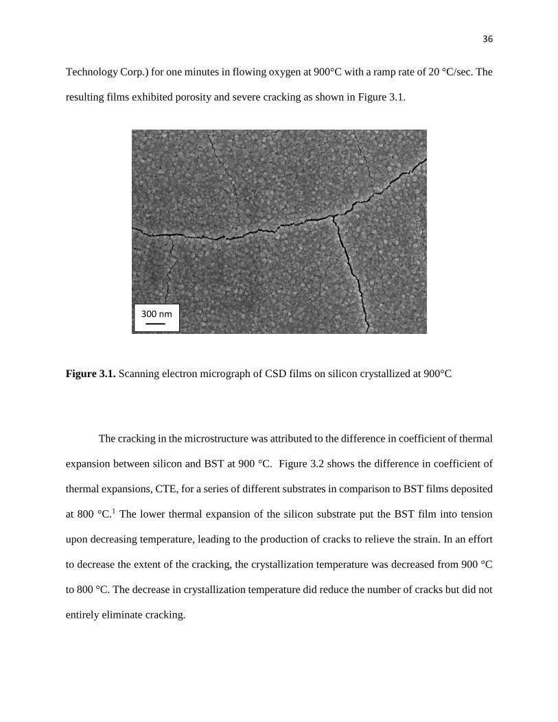
resulting films exhibited porosity and severe cracking as shown in Figure 3.1.
Figure 3.1. Scanning electron micrograph of CSD films on silicon crystallized at 900°C
The cracking in the microstructure was attributed to the difference in coefficient of thermal
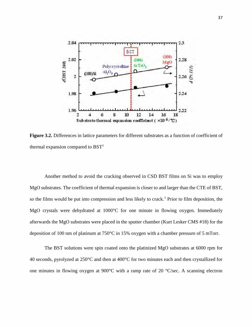
expansion between silicon and BST at 900 °C. Figure 3.2 shows the difference in coefficient of
thermal expansions, CTE, for a series of different substrates in comparison to BST films deposited
at 800 °C.1 The lower thermal expansion of the silicon substrate put the BST film into tension
upon decreasing temperature, leading to the production of cracks to relieve the strain. In an effort
to decrease the extent of the cracking, the crystallization temperature was decreased from 900 °C
to 800 °C. The decrease in crystallization temperature did reduce the number of cracks but did not
entirely eliminate cracking.
300 nm
37
Figure 3.2. Differences in lattice parameters for different substrates as a function of coefficient of
thermal expansion compared to BST1
Another method to avoid the cracking observed in CSD BST films on Si was to employ
MgO substrates. The coefficient of thermal expansion is closer to and larger than the CTE of BST,
so the films would be put into compression and less likely to crack.1 Prior to film deposition, the
MgO crystals were dehydrated at 1000°C for one minute in flowing oxygen. Immediately
afterwards the MgO substrates were placed in the sputter chamber (Kurt Lesker CMS #18) for the
deposition of 100 nm of platinum at 750°C in 15% oxygen with a chamber pressure of 5 mTorr.
The BST solutions were spin coated onto the platinized MgO substrates at 6000 rpm for
40 seconds, pyrolyzed at 250°C and then at 400°C for two minutes each and then crystallized for
one minutes in flowing oxygen at 900°C with a ramp rate of 20 °C/sec. A scanning electron
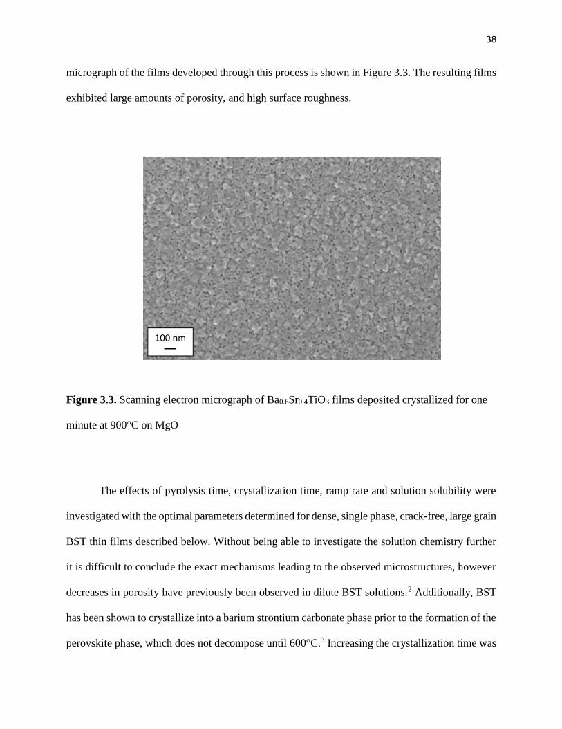
38
micrograph of the films developed through this process is shown in Figure 3.3. The resulting films
exhibited large amounts of porosity, and high surface roughness.
Figure 3.3. Scanning electron micrograph of Ba0.6Sr0.4TiO3 films deposited crystallized for one
minute at 900°C on MgO
The effects of pyrolysis time, crystallization time, ramp rate and solution solubility were
investigated with the optimal parameters determined for dense, single phase, crack-free, large grain
BST thin films described below. Without being able to investigate the solution chemistry further
it is difficult to conclude the exact mechanisms leading to the observed microstructures, however
decreases in porosity have previously been observed in dilute BST solutions.2 Additionally, BST
has been shown to crystallize into a barium strontium carbonate phase prior to the formation of the
perovskite phase, which does not decompose until 600°C.3 Increasing the crystallization time was
100 nm
39
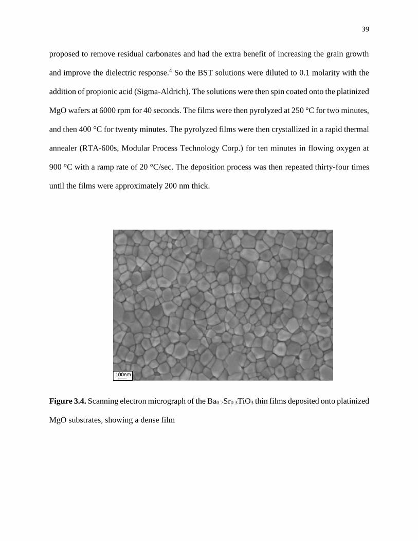
proposed to remove residual carbonates and had the extra benefit of increasing the grain growth
and improve the dielectric response.4 So the BST solutions were diluted to 0.1 molarity with the
addition of propionic acid (Sigma-Aldrich). The solutions were then spin coated onto the platinized
MgO wafers at 6000 rpm for 40 seconds. The films were then pyrolyzed at 250 °C for two minutes,
and then 400 °C for twenty minutes. The pyrolyzed films were then crystallized in a rapid thermal
annealer (RTA-600s, Modular Process Technology Corp.) for ten minutes in flowing oxygen at
900 °C with a ramp rate of 20 °C/sec. The deposition process was then repeated thirty-four times
until the films were approximately 200 nm thick.
Figure 3.4. Scanning electron micrograph of the Ba0.7Sr0.3TiO3 thin films deposited onto platinized
MgO substrates, showing a dense film
40
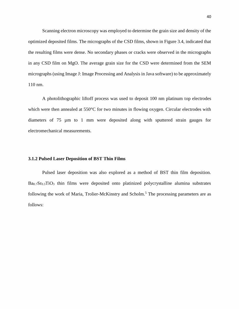
Scanning electron microscopy was employed to determine the grain size and density of the
optimized deposited films. The micrographs of the CSD films, shown in Figure 3.4, indicated that
the resulting films were dense. No secondary phases or cracks were observed in the micrographs
in any CSD film on MgO. The average grain size for the CSD were determined from the SEM
micrographs (using Image J: Image Processing and Analysis in Java software) to be approximately
110 nm.
A photolithographic liftoff process was used to deposit 100 nm platinum top electrodes
which were then annealed at 550°C for two minutes in flowing oxygen. Circular electrodes with
diameters of 75 µm to 1 mm were deposited along with sputtered strain gauges for
electromechanical measurements.
3.1.2 Pulsed Laser Deposition of BST Thin Films
Pulsed laser deposition was also explored as a method of BST thin film deposition.
Ba0.7Sr0.3TiO3 thin films were deposited onto platinized polycrystalline alumina substrates
following the work of Maria, Trolier-McKinstry and Scholm.5 The processing parameters are as
follows:
41
Table 3.1. Pulsed Laser Deposition of BST Films
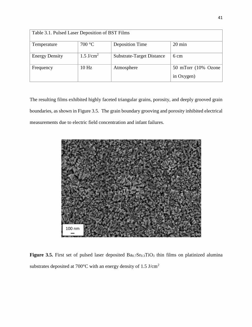
Temperature 700 °C Deposition Time 20 min
Energy Density 1.5 J/cm2 Substrate-Target Distance 6 cm
Frequency 10 Hz Atmosphere 50 mTorr (10% Ozone
in Oxygen)
The resulting films exhibited highly faceted triangular grains, porosity, and deeply grooved grain
boundaries, as shown in Figure 3.5. The grain boundary grooving and porosity inhibited electrical
measurements due to electric field concentration and infant failures.
Figure 3.5. First set of pulsed laser deposited Ba0.7Sr0.3TiO3 thin films on platinized alumina
substrates deposited at 700°C with an energy density of 1.5 J/cm2
100 nm
42
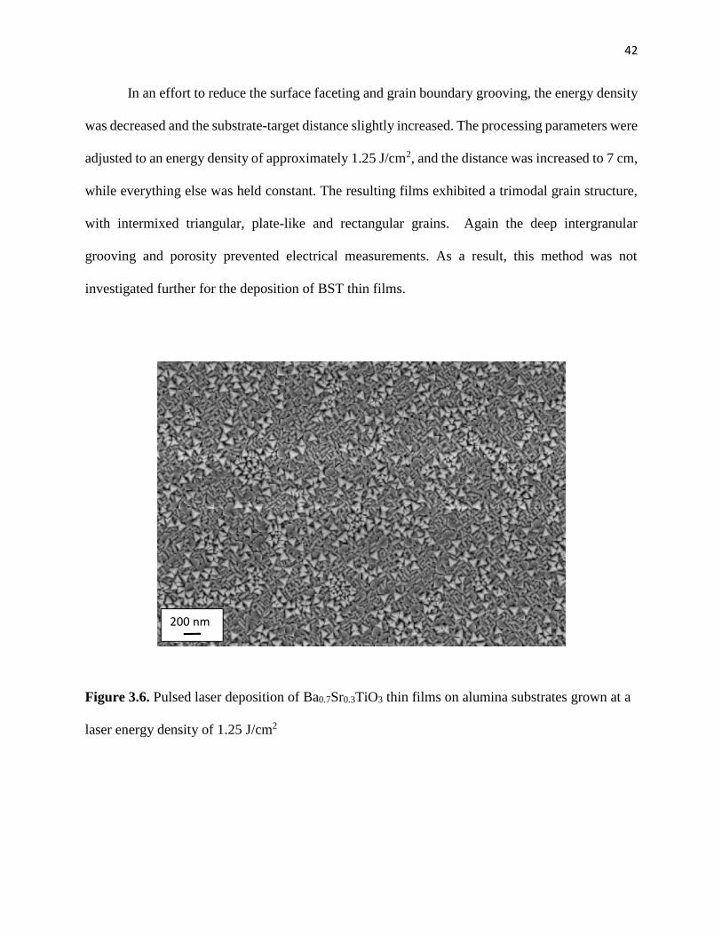
In an effort to reduce the surface faceting and grain boundary grooving, the energy density
was decreased and the substrate-target distance slightly increased. The processing parameters were
adjusted to an energy density of approximately 1.25 J/cm2, and the distance was increased to 7 cm,
while everything else was held constant. The resulting films exhibited a trimodal grain structure,
with intermixed triangular, plate-like and rectangular grains. Again the deep intergranular
grooving and porosity prevented electrical measurements. As a result, this method was not
investigated further for the deposition of BST thin films.
Figure 3.6. Pulsed laser deposition of Ba0.7Sr0.3TiO3 thin films on alumina substrates grown at a
laser energy density of 1.25 J/cm2
200 nm
43
3.1.3. Sputter Deposition of BST Thin Films
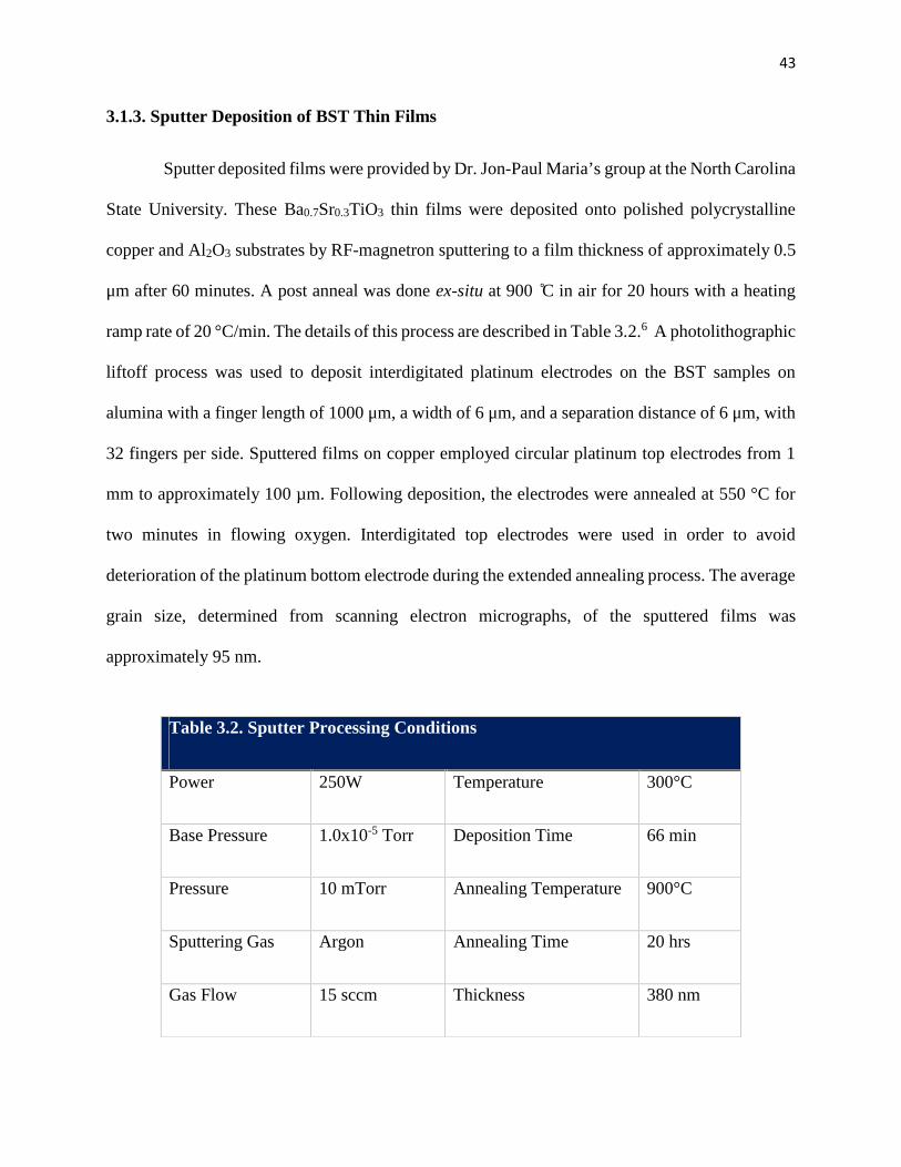
Sputter deposited films were provided by Dr. Jon-Paul Maria’s group at the North Carolina
State University. These Ba0.7Sr0.3TiO3 thin films were deposited onto polished polycrystalline
copper and Al2O3 substrates by RF-magnetron sputtering to a film thickness of approximately 0.5
μm after 60 minutes. A post anneal was done ex-situ at 900 ̊C in air for 20 hours with a heating
ramp rate of 20 °C/min. The details of this process are described in Table 3.2.6 A photolithographic
liftoff process was used to deposit interdigitated platinum electrodes on the BST samples on
alumina with a finger length of 1000 μm, a width of 6 μm, and a separation distance of 6 μm, with
32 fingers per side. Sputtered films on copper employed circular platinum top electrodes from 1
mm to approximately 100 µm. Following deposition, the electrodes were annealed at 550 °C for
two minutes in flowing oxygen. Interdigitated top electrodes were used in order to avoid
deterioration of the platinum bottom electrode during the extended annealing process. The average
grain size, determined from scanning electron micrographs, of the sputtered films was
approximately 95 nm.
Table 3.2. Sputter Processing Conditions
Power 250W Temperature 300°C
Base Pressure 1.0x10⁻⁵ Torr Deposition Time 66 min
Pressure 10 mTorr Annealing Temperature 900°C
Sputtering Gas Argon Annealing Time 20 hrs
Gas Flow 15 sccm Thickness 380 nm
44
3.1.4. Materials from Commercial Sources
Two sets of ceramic BST samples with an approximate composition of Ba0.67Sr0.33TiO3
and Ba0.7Sr0.3TiO3 (as estimated by the temperature dependence of the permittivity), were used as
a point of comparison in the studies on residual ferroelectricity and flexoelectricity. These
materials were developed at Texas Instruments for long wavelength infrared dielectric
microbolometer applications which required strict control of the dielectric response as a function
of temperature.9 As such, although the exact processing parameters are proprietary, it is known
that strict processing control was maintained with regards to the A-site stoichiometry. These same
samples also were used in the work of Ma and Cross in studies on flexoelectricity in BST.9
For the calibration of the e31,f (Electric field and strain) piezoelectric measurement system,
an intrinsically piezoelectric material was required. Lead zirconate titanate thin films were chosen
as the standard for calibration in this study. The films were sputtered lead zirconate titanate,
Pb(Zr0.52Ti0.48)O3, thin films provided by ULVAC Technologies, Inc.. These films were 1 µm in
thickness. Electrode size and deposition method were consistent with the methods used on barium
strontium titanate thin films. Prior to e31,f measurements dielectric and polarization electric field
loops were measured.
3.2 Physical Characterization and Methods
Scanning electron microscopy and x-ray diffraction were used to verify the phase and
quality of the deposited films and ceramics. Transmission electron microscopy was also used in
conjunction with electron energy loss spectroscopy and energy dispersive spectroscopy to
45
investigate the chemical inhomogeneity in BST thin films. Film thickness measurements were
made on a (Tencor 500) profilometer.
3.2.1 Scanning Electron Microscopy
All of the micrographs shown within this section were taken on a Leo 1530 field emission
scanning electron microscope. The working distance was kept within 1.6 - 2.2 mm with an
accelerating electric voltage of 3 kV. An in-lens electron lens was used and no degradation or
charging were observed in subsequent micrographs. Image J software was then used to extract the
average grain size from highly contrasted micrographs.
3.2.2 X-Ray Diffraction
The crystallinity and phase of the BST films were characterized by X-ray diffraction
(PANalytical XPert Pro MPD). Figure 3.7 shows the x-ray diffraction patterns for the CSD and
sputtered Ba0.7Sr0.3TiO3 thin films. In both cases, the patterns were indexed to that of cubic bulk
ceramic BST of the same composition. No second phases or peak splitting, associated with a
ferroelectric phase, were observed in any film. The full width-half maxima of the sputtered films
was over three times that of the CSD films, which might be a result, in part, of differences in
chemical inhomogeneity.
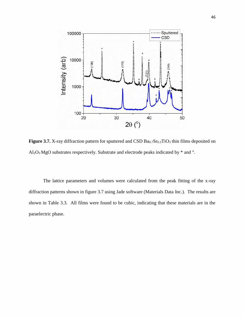
46
Figure 3.7. X-ray diffraction pattern for sputtered and CSD Ba0.7Sr0.3TiO3 thin films deposited on
Al2O3 MgO substrates respectively. Substrate and electrode peaks indicated by * and o.
The lattice parameters and volumes were calculated from the peak fitting of the x-ray
diffraction patterns shown in figure 3.7 using Jade software (Materials Data Inc.). The results are
shown in Table 3.3. All films were found to be cubic, indicating that these materials are in the
paraelectric phase.
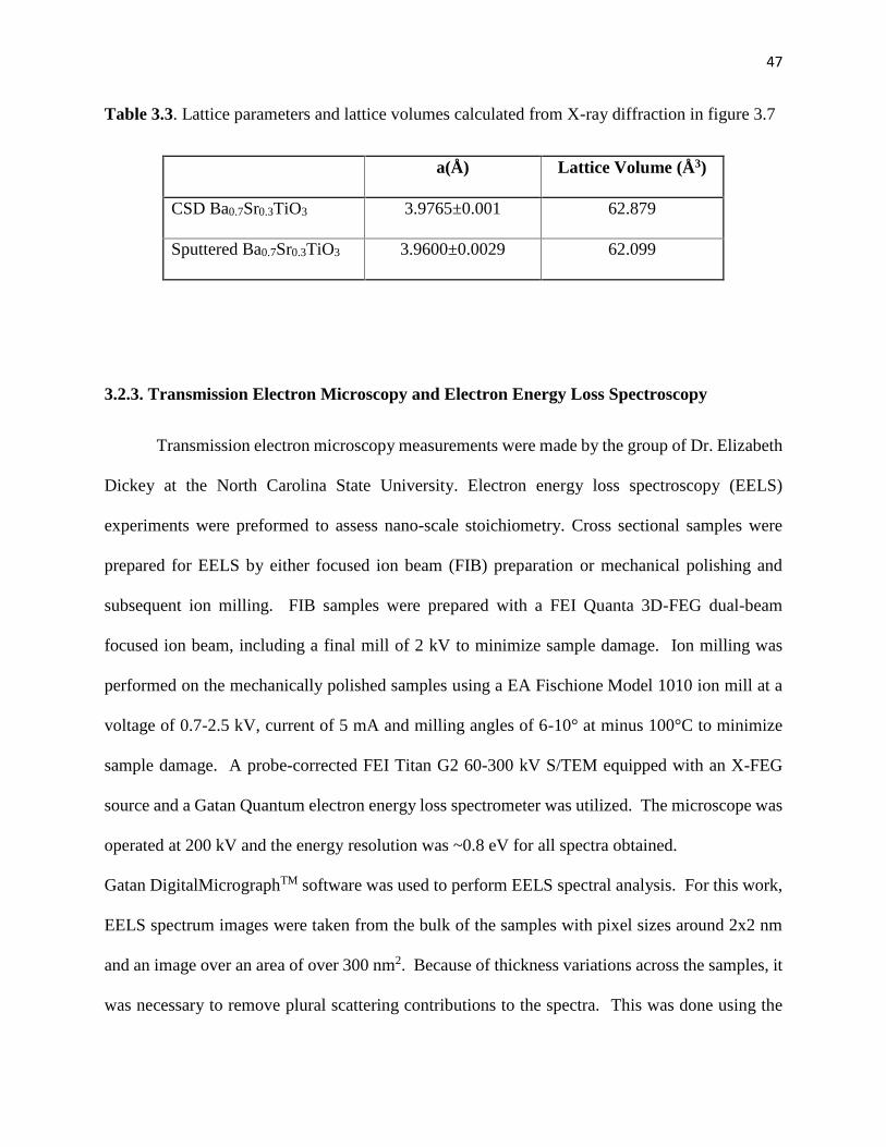
47
Table 3.3. Lattice parameters and lattice volumes calculated from X-ray diffraction in figure 3.7
a(Å) Lattice Volume (Å3)
CSD Ba0.7Sr0.3TiO3 3.9765±0.001 62.879
Sputtered Ba0.7Sr0.3TiO3 3.9600±0.0029 62.099
3.2.3. Transmission Electron Microscopy and Electron Energy Loss Spectroscopy
Transmission electron microscopy measurements were made by the group of Dr. Elizabeth
Dickey at the North Carolina State University. Electron energy loss spectroscopy (EELS)
experiments were preformed to assess nano-scale stoichiometry. Cross sectional samples were
prepared for EELS by either focused ion beam (FIB) preparation or mechanical polishing and
subsequent ion milling. FIB samples were prepared with a FEI Quanta 3D-FEG dual-beam
focused ion beam, including a final mill of 2 kV to minimize sample damage. Ion milling was
performed on the mechanically polished samples using a EA Fischione Model 1010 ion mill at a
voltage of 0.7-2.5 kV, current of 5 mA and milling angles of 6-10° at minus 100°C to minimize
sample damage. A probe-corrected FEI Titan G2 60-300 kV S/TEM equipped with an X-FEG
source and a Gatan Quantum electron energy loss spectrometer was utilized. The microscope was
operated at 200 kV and the energy resolution was ~0.8 eV for all spectra obtained.
Gatan DigitalMicrographTM software was used to perform EELS spectral analysis. For this work,
EELS spectrum images were taken from the bulk of the samples with pixel sizes around 2x2 nm
and an image over an area of over 300 nm2. Because of thickness variations across the samples, it
was necessary to remove plural scattering contributions to the spectra. This was done using the
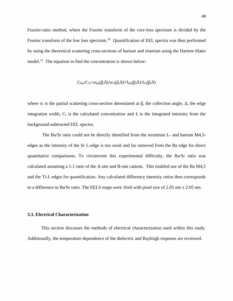
48
Fourier-ratio method, where the Fourier transform of the core-loss spectrum is divided by the
Fourier transform of the low loss spectrum.10 Quantification of EEL spectra was then performed
by using the theoretical scattering cross-sections of barium and titanium using the Hartree-Slater
model.11 The equation to find the concentration is shown below:
CBa/CTi=σBa(β,∆)/σTi(β,∆)×IBa(β,∆)/ITi(β,∆)
where σi is the partial scattering cross-section determined at β, the collection angle, Δ, the edge
integration width, Ci is the calculated concentration and Ii is the integrated intensity from the
background-subtracted EEL spectra.
The Ba/Sr ratio could not be directly identified from the strontium L- and barium M4,5-
edges as the intensity of the Sr L-edge is too weak and far removed from the Ba edge for direct
quantitative comparisons. To circumvent this experimental difficulty, the Ba/Sr ratio was
calculated assuming a 1:1 ratio of the A-site and B-site cations. This enabled use of the Ba M4,5
and the Ti-L edges for quantification. Any calculated difference intensity ratios then corresponds
to a difference in Ba/Sr ratio. The EELS maps were 16x6 with pixel size of 2.05 nm x 2.05 nm.
3.3. Electrical Characterization
This section discusses the methods of electrical characterization used within this study.
Additionally, the temperature dependence of the dielectric and Rayleigh response are reviewed.
49
3.3.1. Dielectric Measurements
Capacitance and dielectric loss tangent were measured on six to ten electrodes for each sample
prior to other electrical measurements. With the thickness, t, and electrode area, A, known, the
permittivity can be calculated from the capacitance from:
=where εo is the permittivity of free space.12 All capacitance and loss tangent measurements were
taken at 1 kHz and 30 mV unless otherwise specified. All dielectric and tunable measurements
were taken on a precision LCR meter (Hewlett Packard 4284A).
Thin film dielectric temperature dependence was measured using a Peltier heating stage
(Temptronic) on a Cascade Probe Station. The temperature was monitored by a type-K
thermocouple on the surface of the sample, and read via a digital multimeter (Hewlett Packard
3478). The sample were first heated above the Tmax, approximately 50 °C, prior to any temperature
measurement. Temperature measurements were taken first on increasing then decreasing
temperature over the temperature range from -60 °C to 200 °C. For ceramic measurements the
temperature response was measured with a Delta design 2300 heating/cooling oven, monitored by
again by a type-k thermocouple.
3.3.2. Rayleigh Analysis
Rayleigh analysis was conducted as a function of temperature and frequency using a precision
LCR meter (Hewlett Packard 4284A). For thin film measurements, the heating and cooling were
50
controlled by a Peltier heater, monitored by a type-K thermocouple on the surface of the sample,
and read via a digital multimeter (Hewlett Packard 3478). Samples were allowed to equilibrate for
five minutes at the highest temperature. Subsequent temperature steps had a tolerance of 1 °C with
a hold for two minutes before making a measurement. The temperature range was chosen to span
the global transition temperature determined from the dielectric temperature response. Rayleigh
behavior was characterized from 100 Hz to 1 MHz.
3.3.3 Current-Voltage Measurements
Leakage current measurements were taken on a 4140 pico-Ampere Meter/DC Voltage
Source (Hewlett Packard). Prior to any current-voltage measurements, the time dependent current
under constant voltage was measured in order to determine the steady state conditions.
Temperature dependent leakage current measurements were acquired using the same methodology
as is used for measuring dielectric temperature dependence.
3.3.4 Polarization-Electric Field Loops
Thin film polarization-electric field measurements were taken on a Precision Multiferroic
materials analyzer (Radiant Technologies, Inc.). Measurements were made on increasing voltage
to failure in increments of 1 V for minor loops and 20 V for major loops. All reported data is the
average of ten consecutive, electric field sweeps with the same initial polarity. The frequency of
the applied electric field was 100 Hz unless otherwise specified. For bulk polarization-electric
51
field data, measurements were taken on custom charge integrator in conjunction with an amplifier
(Kepco Power Supplies).
3.4. Other Measurements
3.4.1. Second Harmonic Generation
Second harmonic generation was conducted in barium strontium titanate ceramics and thin
films. An Instec Inc. temperature system with liquid nitrogen coolant was used to control the
sample temperature. A 800 nm 90 femtosecond laser (Coherent Inc) was used with a final
frequency of 2 kHz. The sample was placed 8.5 cm away from the focus. The signal was collected
by a photo multiplier tube (Hamamatsu H7826) and a lock-in amplifier with a 4.65 kΩ with an OD
filter of 0.3-1.5.
3.4.2. Piezoresponse Force Microscopy
Piezoresponse force microscopy, PFM, was conducted on barium strontium titanate based
ceramic samples provided by Texas Instruments. Samples were cut from the BST bulk ceramics
and prepared for PFM by polishing. Samples were mounted onto a polishing disc with crystal
bond and bounded on each side with a glass slide in order to insure level polishing as shown in
Figure 3.8. The samples were polished with 30 µm, 15 µm and 9 µm Al2O3 grit for approximately
three minutes each, followed by 6 µm, 3 µm, 1 µm diamond grit for ten to fifteen minutes each
and then 0.5 µm diamond grit for thirty minutes to an hour. One sample set was then annealed at
approximately 275 °C for 2 hours to remove residual surface strain induced during polishing.
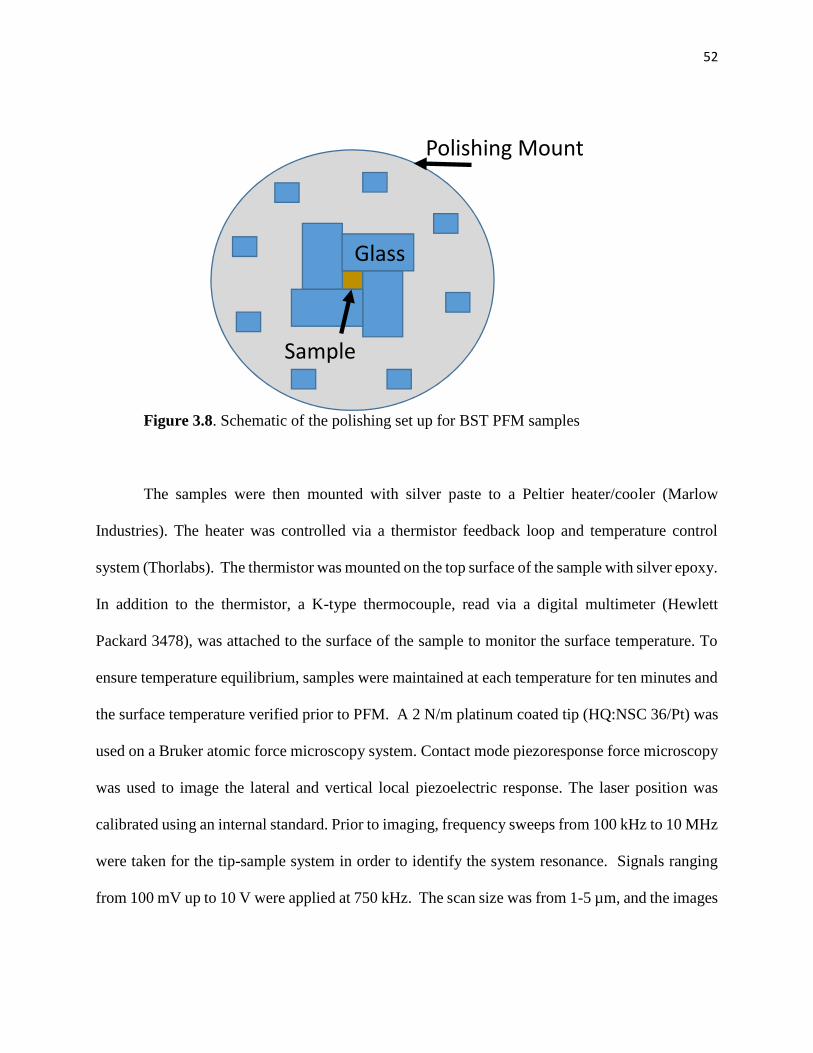
52
Figure 3.8. Schematic of the polishing set up for BST PFM samples
The samples were then mounted with silver paste to a Peltier heater/cooler (Marlow
Industries). The heater was controlled via a thermistor feedback loop and temperature control
system (Thorlabs). The thermistor was mounted on the top surface of the sample with silver epoxy.
In addition to the thermistor, a K-type thermocouple, read via a digital multimeter (Hewlett
Packard 3478), was attached to the surface of the sample to monitor the surface temperature. To
ensure temperature equilibrium, samples were maintained at each temperature for ten minutes and
the surface temperature verified prior to PFM. A 2 N/m platinum coated tip (HQ:NSC 36/Pt) was
used on a Bruker atomic force microscopy system. Contact mode piezoresponse force microscopy
was used to image the lateral and vertical local piezoelectric response. The laser position was
calibrated using an internal standard. Prior to imaging, frequency sweeps from 100 kHz to 10 MHz
were taken for the tip-sample system in order to identify the system resonance. Signals ranging
from 100 mV up to 10 V were applied at 750 kHz. The scan size was from 1-5 µm, and the images
Sample
Glass
Polishing Mount
53
were made by scanning at 90° angle to the cantilever length. Images were taken in approximately
the same location for every temperature set.
3.5. References
1. Ito, S., Funakubo, H., Koutsaroff, I. P., Zelner, M. & Cervin-Lawry, A. Effect of the thermal
expansion matching on the dielectric tunability of (100)-one-axis-oriented (Ba0.5Sr0.5)TiO3 thin
films. Appl. Phys. Lett. 90, 142910–142910–3 (2007).
2. Hoffmann, S. & Waser, R. Control of the morphology of CSD-prepared (Ba,Sr)TiO3 thin films.
J. Eur. Ceram. Soc. 19, 1339–1343 (1999).
3. Gust, M. C., Momoda, L. A., Evans, N. D. & Mecartney, M. L. Crystallization of Sol–Gel-
Derived Barium Strontium Titanate Thin Films. J. Am. Ceram. Soc. 84, 1087–1092 (2001).
4. Tahan, D. M., Safari, A. & Klein, L. C. Preparation and Characterization of BaxSr1-xTiO3 Thin
Films by a Sol-Gel Technique. J. Am. Ceram. Soc. 79, 1593–1598 (1996).
5. Maria, J.-P., Trolier-McKinstry, S. & Schlom, D. G. Size effects in barium titanate thin film
heterostructures with conductive oxide electrodes. in Proc. Tenth IEEE Int. Symp. Appl.
Ferroelectr. 1996 ISAF 96 1, 333–336 vol.1 (1996).
6. P.G. Lam, V. Haridasan, M.B. Steer, A.I. Kingon, and J.-P. Maria. IEEE Transactions on
Ultrasonics, Ferroelectrics and Frequency Control 59, 198–204 (2012).
7. Park, J. H., Xu, F. & Trolier-McKinstry, S. Dielectric and piezoelectric properties of sol–gel
derived lead magnesium niobium titanate films with different textures. J. Appl. Phys. 89, 568–
574 (2001).
54
8. Keech, R., Shetty, S., Kuroda, M. A., Liu, X. H., Martyna, G. J., Newns, D. M., Trolier-
McKinstry, S Lateral scaling of Pb(Mg1/3Nb2/3)O3-PbTiO3 thin films for piezoelectric logic
applications. J. Appl. Phys. 115, 234106 (2014).
9. Ma, W. & Cross, L. E. Flexoelectric polarization of barium strontium titanate in the paraelectric
state. Appl. Phys. Lett. 81, 3440–3442 (2002).
10. Egerton, R. F. & Whelan, M. J. The electron energy loss spectrum and band structure of
diamond, Springer, New York, (1974).
11. Slater, J.C. A simplification of the Hartree-Fock method. Phys Rev. 81. 3, 385 (1951).
12. Moulson, A. J., Herbert, J. M. Electroceramics: Materials, Properties, Applications. (John
Wiley & Sons, 2003).
55
Chapter 4
e31,f (Electric Field and Strain)
4.1. Introduction
Barium strontium titanate thin film tunable dielectrics are becoming a viable technology for
frequency agile applications, but still suffer from comparatively high loss in the microwave
region.1,2 Although nominally operated in the cubic paraelectric phase the application of a DC
electric field to a barium strontium titanate, BST, thin film during tuning spoils the center of
symmetry, allowing for the development of piezoelectric responses.3,4 Electric field induced
piezoelectricity creates resonances detectable in the impedance spectra which act as a loss
mechanism in tunable dielectrics, or as an active property in tunable thin film bulk acoustic
resonators.5 Resonances in the low GHz have previously been reported for 200-400 nm thick BST
thin films, well within the frequencies of interest for RF tunable applications.6 Avoiding or
employing induced piezoelectric resonances necessitates predictive models of the impedance
response over the frequencies and electric fields of interest.3,7 Modeling the induced piezoelectric
impedance resonances requires an understanding of the material response under electric field,
which is rarely directly measured.6,7
This work provides direct measurements of the DC electric field induced e31,f piezoelectric
response and tunability for barium strontium titanate, BST, thin films with different compositions
and varied strain states. The electric field dependence of the piezoelectric and dielectric response
is related to the development of induced piezoelectric resonances through the piezoelectric
coupling coefficient, k which is determined from:
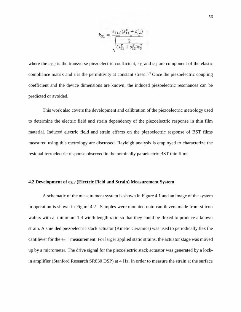
56
= , ( + )2( + )where the e31,f is the transverse piezoelectric coefficient, s11 and s12 are component of the elastic
compliance matrix and ε is the permittivity at constant stress.8,9 Once the piezoelectric coupling
coefficient and the device dimensions are known, the induced piezoelectric resonances can be
predicted or avoided.
This work also covers the development and calibration of the piezoelectric metrology used
to determine the electric field and strain dependency of the piezoelectric response in thin film
material. Induced electric field and strain effects on the piezoelectric response of BST films
measured using this metrology are discussed. Rayleigh analysis is employed to characterize the
residual ferroelectric response observed in the nominally paraelectric BST thin films.
4.2 Development of e31,f (Electric Field and Strain) Measurement System
A schematic of the measurement system is shown in Figure 4.1 and an image of the system
in operation is shown in Figure 4.2. Samples were mounted onto cantilevers made from silicon
wafers with a minimum 1:4 width:length ratio so that they could be flexed to produce a known
strain. A shielded piezoelectric stack actuator (Kinetic Ceramics) was used to periodically flex the
cantilever for the e31,f measurement. For larger applied static strains, the actuator stage was moved
up by a micrometer. The drive signal for the piezoelectric stack actuator was generated by a lock-
in amplifier (Stanford Research SR830 DSP) at 4 Hz. In order to measure the strain at the surface
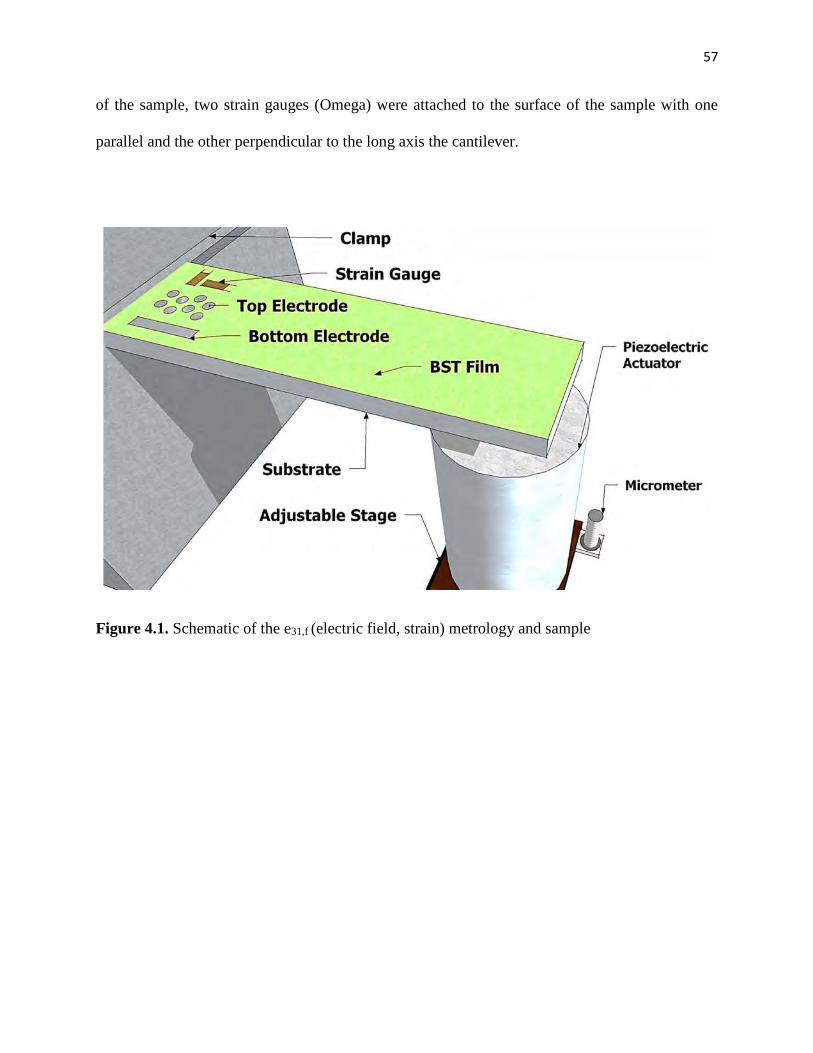
57
of the sample, two strain gauges (Omega) were attached to the surface of the sample with one
parallel and the other perpendicular to the long axis the cantilever.
Figure 4.1. Schematic of the e31,f (electric field, strain) metrology and sample
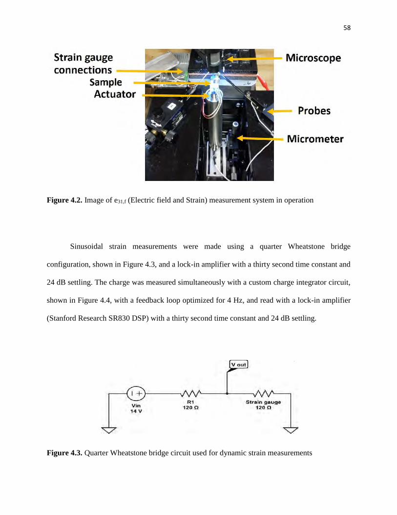
58
Figure 4.2. Image of e31,f (Electric field and Strain) measurement system in operation
Sinusoidal strain measurements were made using a quarter Wheatstone bridge
configuration, shown in Figure 4.3, and a lock-in amplifier with a thirty second time constant and
24 dB settling. The charge was measured simultaneously with a custom charge integrator circuit,
shown in Figure 4.4, with a feedback loop optimized for 4 Hz, and read with a lock-in amplifier
(Stanford Research SR830 DSP) with a thirty second time constant and 24 dB settling.
Figure 4.3. Quarter Wheatstone bridge circuit used for dynamic strain measurements
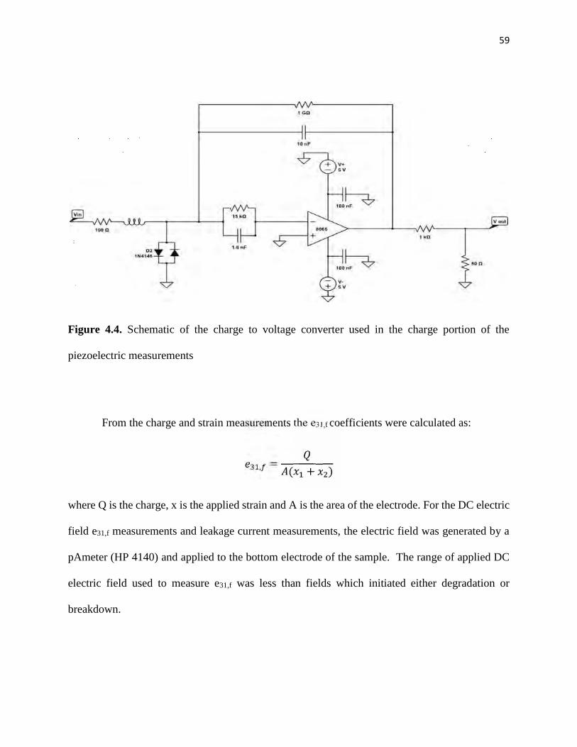
59
Figure 4.4. Schematic of the charge to voltage converter used in the charge portion of the
piezoelectric measurements
From the charge and strain measurements the e31,f coefficients were calculated as:
, = ( + )where Q is the charge, x is the applied strain and A is the area of the electrode. For the DC electric
field e31,f measurements and leakage current measurements, the electric field was generated by a
pAmeter (HP 4140) and applied to the bottom electrode of the sample. The range of applied DC
electric field used to measure e31,f was less than fields which initiated either degradation or
breakdown.
60
4.3 Calibration of the e31,f (Electric field and Strain) Measurement System
The uniaxial e31,f(Electric field and Strain) measurement system was calibrated against a
biaxial e31,f measurements system. An intrinsically piezoelectric thin film was used as standard. A
1µm thick, sputtered Pb(Zr0.52Ti0.48)O3, (ULVAC Technologies Inc.), film was used as this
standard. Sample from this film were mounted onto silicon wafers or cantilevers for either the
biaxial or uniaxial measurements respectively. Two strain gauges (Omega) were attached to the
surface of the samples with a cyanoacrylate-based glue. For the uniaxial system these gauges were
oriented parallel and perpendicular to the long axis the cantilever. Prior to strain measurements the
resistance of the gauge was verified to be within 120 ±1 Ohms. In both measurement systems, the
drive signal was generated by a lock-in amplifier (Stanford Research SR830 DSP). To make
concurrent strain and charge measurements, three lock-ins where connected together and the
settings for each were kept at 4 Hz, with a 30 second time constant, and a 24 dB settling time. In
both measurement systems, the samples were poled at 15 V for 15 minutes and were let sit for ten
minutes prior to making measurements. The phase output was used to gauge the quality of the
strain gauge attachment or thin film response. Calibration samples were limited to those with less
than ten degrees phase output for the strain gauges and greater than 170 degrees for the charge
output. Dynamic strain measurements were made using a quarter Wheatstone bridge configuration,
shown in Figure 4.3 and the charge measurements were made simultaneously with a custom charge
integrator circuit, shown in Figure 4.4, with a feedback loop optimized for 4 Hz. The output from
the e31,f(Electric field and Strain) strain and charge measurement circuits were simultaneous
checked against the exact same circuits used in the biaxial e31,f measurement system. No
significant differences were observed between the measurement circuits.
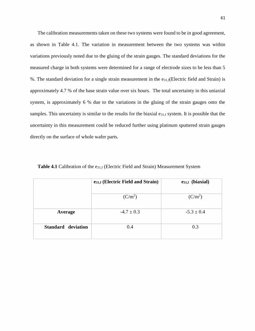
61
The calibration measurements taken on these two systems were found to be in good agreement,
as shown in Table 4.1. The variation in measurement between the two systems was within
variations previously noted due to the gluing of the strain gauges. The standard deviations for the
measured charge in both systems were determined for a range of electrode sizes to be less than 5
%. The standard deviation for a single strain measurement in the e31,f(Electric field and Strain) is
approximately 4.7 % of the base strain value over six hours. The total uncertainty in this uniaxial
system, is approximately 6 % due to the variations in the gluing of the strain gauges onto the
samples. This uncertainty is similar to the results for the biaxial e31,f system. It is possible that the
uncertainty in this measurement could be reduced further using platinum sputtered strain gauges
directly on the surface of whole wafer parts.
Table 4.1 Calibration of the e31,f (Electric Field and Strain) Measurement System
e31,f (Electric Field and Strain) e31,f (biaxial)
(C/m2) (C/m2)
Average -4.7 ± 0.3 -5.3 ± 0.4
Standard deviation 0.4 0.3
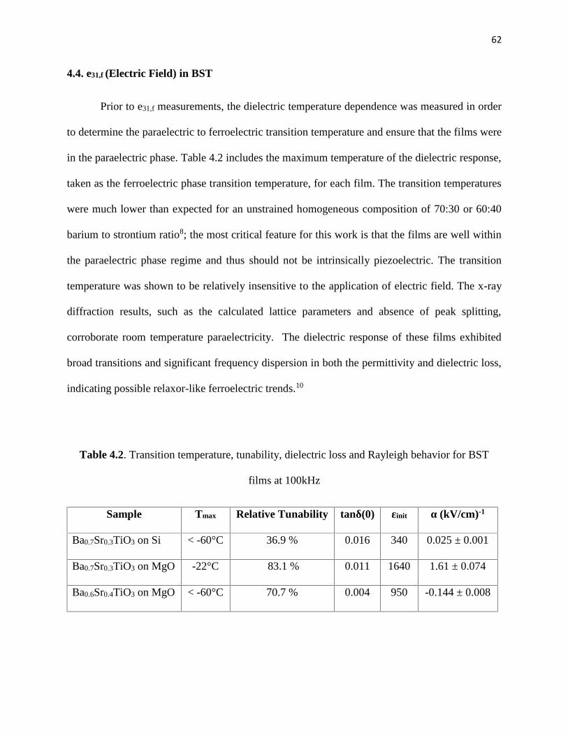
62
4.4. e31,f (Electric Field) in BST
Prior to e31,f measurements, the dielectric temperature dependence was measured in order
to determine the paraelectric to ferroelectric transition temperature and ensure that the films were
in the paraelectric phase. Table 4.2 includes the maximum temperature of the dielectric response,
taken as the ferroelectric phase transition temperature, for each film. The transition temperatures
were much lower than expected for an unstrained homogeneous composition of 70:30 or 60:40
barium to strontium ratio8; the most critical feature for this work is that the films are well within
the paraelectric phase regime and thus should not be intrinsically piezoelectric. The transition
temperature was shown to be relatively insensitive to the application of electric field. The x-ray
diffraction results, such as the calculated lattice parameters and absence of peak splitting,
corroborate room temperature paraelectricity. The dielectric response of these films exhibited
broad transitions and significant frequency dispersion in both the permittivity and dielectric loss,
indicating possible relaxor-like ferroelectric trends.10
Table 4.2. Transition temperature, tunability, dielectric loss and Rayleigh behavior for BST
films at 100kHz
Sample Tmax Relative Tunability tanδ(0) εinit α (kV/cm)-1
Ba0.7Sr0.3TiO3 on Si < -60°C 36.9 % 0.016 340 0.025 ± 0.001
Ba0.7Sr0.3TiO3 on MgO -22°C 83.1 % 0.011 1640 1.61 ± 0.074
Ba0.6Sr0.4TiO3 on MgO < -60°C 70.7 % 0.004 950 -0.144 ± 0.008
63
The electric field induced e31,f piezoelectric response for the BST thin films is shown in Figure
4.5. All samples in this study displayed a finite unbiased piezoelectric response despite being
within the paraelectric phase regime. Each film went through a minima on increasing and
decreasing field at approximately 10 kV/cm, implying an initial preferred polarization state. For
all samples, uncertainty in the field induced e31,f response increased with increasing applied electric
field even though the applied electric field was kept below the electric fields need for degradation
determined by prior leakage current measurements. Field induced e31,f for the 60:40 BST on MgO
and the 70:30 BST on Si films were both comparatively linear with a slope of 2.6 × 10 and1.4 × 10 C/kVm respectively from 10-120 kV/cm. The 70:30 BST films on MgO exhibited
significant hysteresis on sweeping applied electric field, which is consistent with the alignment of
ferroelectric domains.8 The BST 70:30 films on MgO displayed a larger initial slope; the induced
e31,f value saturated above 70 kV/cm, reaching a value similar to that of the 60:40 BST films.
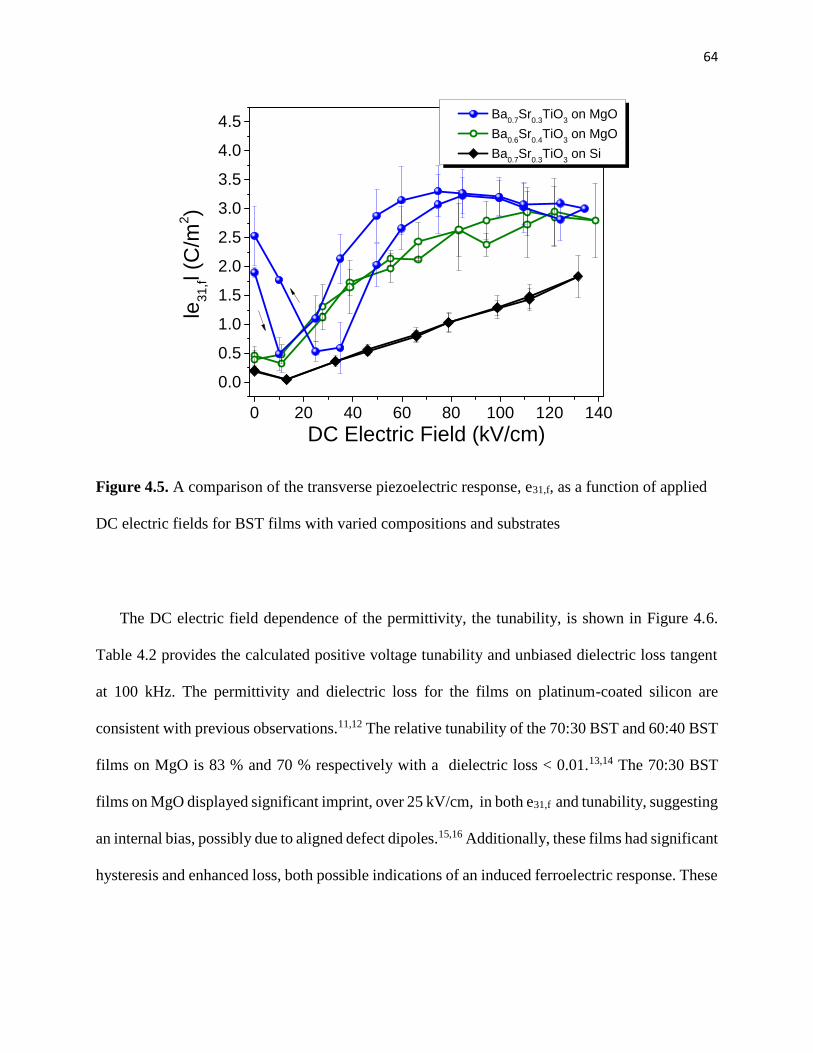
64
0 20 40 60 80 100 120 140
0.0
0.5
1.0
1.5
2.0
2.5
3.0
3.5
4.0
4.5
le31
,fl (C
/m2 )
DC Electric Field (kV/cm)
Ba0.7Sr0.3TiO3 on MgO Ba0.6Sr0.4TiO3 on MgO Ba0.7Sr0.3TiO3 on Si
Figure 4.5. A comparison of the transverse piezoelectric response, e31,f, as a function of applied
DC electric fields for BST films with varied compositions and substrates
The DC electric field dependence of the permittivity, the tunability, is shown in Figure 4.6.
Table 4.2 provides the calculated positive voltage tunability and unbiased dielectric loss tangent
at 100 kHz. The permittivity and dielectric loss for the films on platinum-coated silicon are
consistent with previous observations.11,12 The relative tunability of the 70:30 BST and 60:40 BST
films on MgO is 83 % and 70 % respectively with a dielectric loss < 0.01.13,14 The 70:30 BST
films on MgO displayed significant imprint, over 25 kV/cm, in both e31,f and tunability, suggesting
an internal bias, possibly due to aligned defect dipoles.15,16 Additionally, these films had significant
hysteresis and enhanced loss, both possible indications of an induced ferroelectric response. These
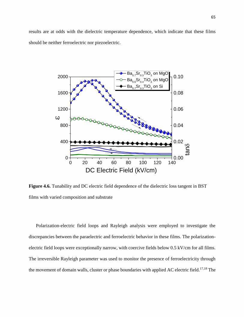
65
results are at odds with the dielectric temperature dependence, which indicate that these films
should be neither ferroelectric nor piezoelectric.
0 20 40 60 80 100 120 1400
400
800
1200
1600
2000
DC Electric Field (kV/cm)
Ba0.7Sr0.3TiO3 on MgO Ba0.6Sr0.4TiO3 on MgO Ba0.7Sr0.3TiO3 on Si
0.00
0.02
0.04
0.06
0.08
0.10
tan
Figure 4.6. Tunability and DC electric field dependence of the dielectric loss tangent in BST
films with varied composition and substrate
Polarization-electric field loops and Rayleigh analysis were employed to investigate the
discrepancies between the paraelectric and ferroelectric behavior in these films. The polarization-
electric field loops were exceptionally narrow, with coercive fields below 0.5 kV/cm for all films.
The irreversible Rayleigh parameter was used to monitor the presence of ferroelectricity through
the movement of domain walls, cluster or phase boundaries with applied AC electric field.17,18 The
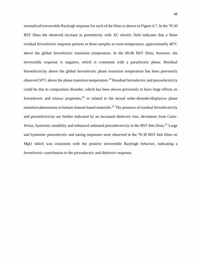
66
normalized irreversible Rayleigh response for each of the films is shown in Figure 4.7. In the 70:30
BST films the observed increase in permittivity with AC electric field indicates that a finite
residual ferroelectric response persists in these samples at room temperature, approximately 40°C
above the global ferroelectric transition temperature. In the 60:40 BST films, however, the
irreversible response is negative, which is consistent with a paraelectric phase. Residual
ferroelectricity above the global ferroelectric phase transition temperature has been previously
observed 50°C above the phase transition temperature.19 Residual ferroelectric and piezoelectricity
could be due to composition disorder, which has been shown previously to have large effects on
ferroelectric and relaxor properties,20 or related to the mixed order-disorder/displacive phase
transition phenomena in barium titanate based materials.21 The presence of residual ferroelectricity
and piezoelectricity are further indicated by an increased dielectric loss, deviations from Curie-
Weiss, hysteretic tunability and enhanced unbiased piezoelectricity in the BST thin films.22 Large
and hysteretic piezoelectric and tuning responses were observed in the 70:30 BST thin films on
MgO which was consistent with the positive irreversible Rayleigh behavior, indicating a
ferroelectric contribution to the piezoelectric and dielectric response.
67
0 2 4 6 8 10 12 14-2
0
2
4
6
8
10
Nor
mal
ized
Ray
leig
h R
espo
nse
EAC(kV/cm)
Ba0.7Sr0.3TiO3 on MgO Ba0.7Sr0.3TiO3 on Si Ba0.6Sr0.4TiO3 on MgO
Figure 4.7. Normalized irreversible Rayleigh behavior for 70:30 BST on MgO and Si, and 60:40
BST on MgO thin films
The application of the DC electric field does not significantly impact Tmax of the BST 70:30
or 80:20 thin films on MgO determined from the dielectric temperature dependence. For the 80:20
films the maximum in permittivity with temperature was suppressed nearly 5 °C with the
application of approximately 200 kV/cm. No significant shift was observed in the BST 70:30 or
60:40 thin films on MgO. This indicates that the observed ferroelectric response is not due to a
shifting of the ferroelectric transition temperature to room temperatures, over 40 °C for the 70:30
films, under dc bias.
68
4.5. e31,f (Electric Field and Strain) in BST
Measurements were also taken as a function of static applied strain, through the fixed
displacement of the piezoelectric actuator, comparable to piezoelectric systems designed by
Dubois and Muralt.9 The circuit for the DC strain measurements is provided in Figure 4.8. The
strain was calculated from these circuits using the following:
= ( ) − ( )∗ ( )= −4∗ (1 + 2 )
where Vout(strained) and Vout(unstrained) are the voltage output of a strain gauge under the and prior to
the application of strain. x is the calculated strain. Vex is the excitation voltage used at the input
of the Wheatstone bridge and Gain is the gain from the instrumentation amplifier used to increase
the signal to noise ratio. GF stands for the gauge factor of the strain gauges, which for the Omega
two dimensional gauges used in this study were 1.91 ±1.0% and 1.95 ±1.0% for the parallel and
perpendicular gauges, respectively. Prior to static strain measurements the full Wheatstone bridge
was balanced so that the unstrained gauge output was zero.
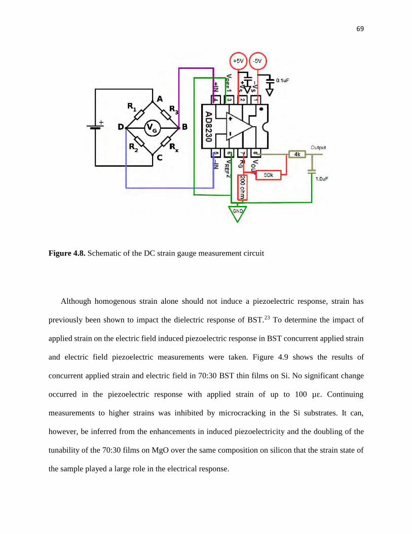
69
Figure 4.8. Schematic of the DC strain gauge measurement circuit
Although homogenous strain alone should not induce a piezoelectric response, strain has
previously been shown to impact the dielectric response of BST.23 To determine the impact of
applied strain on the electric field induced piezoelectric response in BST concurrent applied strain
and electric field piezoelectric measurements were taken. Figure 4.9 shows the results of
concurrent applied strain and electric field in 70:30 BST thin films on Si. No significant change
occurred in the piezoelectric response with applied strain of up to 100 µε. Continuing
measurements to higher strains was inhibited by microcracking in the Si substrates. It can,
however, be inferred from the enhancements in induced piezoelectricity and the doubling of the
tunability of the 70:30 films on MgO over the same composition on silicon that the strain state of
the sample played a large role in the electrical response.
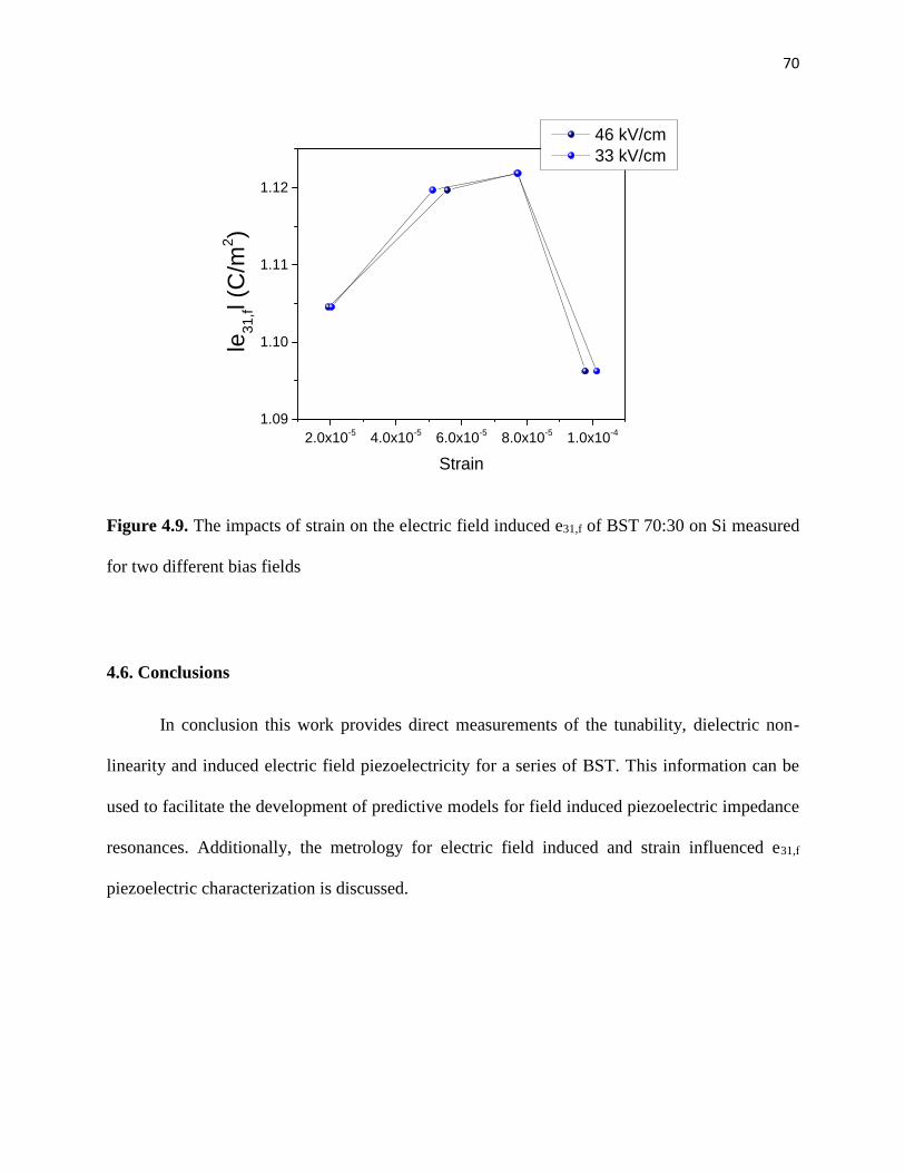
70
2.0x10⁻⁵ 4.0x10⁻⁵ 6.0x10⁻⁵ 8.0x10⁻⁵ 1.0x10-41.09
1.10
1.11
1.12
le31
,fl (C
/m2 )
Strain
46 kV/cm 33 kV/cm
Figure 4.9. The impacts of strain on the electric field induced e31,f of BST 70:30 on Si measured
for two different bias fields
4.6. Conclusions
In conclusion this work provides direct measurements of the tunability, dielectric non-
linearity and induced electric field piezoelectricity for a series of BST. This information can be
used to facilitate the development of predictive models for field induced piezoelectric impedance
resonances. Additionally, the metrology for electric field induced and strain influenced e31,f
piezoelectric characterization is discussed.
71
4.7. References
1. Tagantsev, A. K., Sherman, V. O., Astafiev, K. F., Venkatesh, J. & Setter, N. Ferroelectric
materials for microwave tunable applications. J. Electroceramics 11, 5–66 (2003).
2. York, R. A., “Tunable Dielectrics for RF Circuits”, Multifunctional adaptive microwave
circuits and systems, M. Steer, W. D. Palmer (Editors), SciTech Publishing, (2009).
3. Noeth, A., Yamada, T., Tagantsev, A. K. & Setter, N. Electrical tuning of dc bias induced
acoustic resonances in paraelectric thin films. J. Appl. Phys. 104, 094102 (2008).
4. Morito, K., Iwazaki, Y., Suzuki, T. & Fujimoto, M. Electric field induced piezoelectric
resonance in the micrometer to millimeter waveband in a thin film SrTiO3 capacitor. J. Appl.
Phys. vol. 94, no. 8, pp. 5199–5205, Oct. 2003.
5. Noeth, A., Yamada, T., Muralt, P., Tagantsev, A. K. & Setter, N., Tunable thin film bulk
acoustic wave resonator based on BaxSr1-xTiO3 thin film, IEEE Trans. Ultrason. Ferroelectr.
Freq. Control, vol. 57, no. 2, pp. 379–385, Feb. 2010.
6. Giere, A., Schafranek, R., Zheng, Y., Maune, H., Sazegar, M., Jakoby, R., Klein, A.
Characterization of acoustic effects in ferroelectric thin-films for microwave components.
Frequenz 62, 52–56 (2008).
7. Vendik, I. B., Turalchuk, P. A., Vendik, O. G. & Berge, J. Modeling tunable bulk acoustic
resonators based on induced piezoelectric effect in BaTiO3 and Ba0.25Sr0.75TiO3 films, J. Appl.
Phys., vol. 103, no. 1, p. 014107, Jan. 2008.
8. Jaffe, B., Cook, W. R. & Jaffe, H. L. Piezoelectric ceramics. (Academic Press, 1971).
9. Dubois, M.-A. & Muralt, P. Measurement of the effective transverse piezoelectric coefficient
e31,f of AlN and Pb(Zrx,Ti1−x)O3 thin films,” Sens. Actuators Phys., vol. 77, no. 2, pp. 106–
112, Oct. 1999.
72
10. Viehland, D., Jang, S. J., Cross, L. E. & Wuttig, M. Deviation from Curie-Weiss behavior in
relaxor ferroelectrics. Phys. Rev. B 46, 8003–8006 (1992).
11. Tahan, D. M., Safari, A. & Klein, L. C. Preparation and characterization of BaxSr1-xTiO3 thin
films by a sol-gel technique. J. Am. Ceram. Soc. 79, 1593–1598 (1996).
12. Li, H., Roytburd, A. L., Alpay, S. P., Tran, T. D., Salamanca-Riba, L., and Ramesh, R.
Dependence of dielectric properties on internal stresses in epitaxial barium strontium titanate
thin films. Appl. Phys. Lett. 78, 2354–2356 (2001).
13. Ito, S., Funakubo, H., Koutsaroff, I. P., Zelner, M. & Cervin-Lawry, A. Effect of the thermal
expansion matching on the dielectric tunability of (100)-one-axis-oriented (Ba0.5Sr0.5)TiO3
thin films. Appl. Phys. Lett. 90, 142910–142910–3 (2007).
14. Tiggelman, M. P. J., Reimann, K., Van Rijs, F., Schmitz, J. & Hueting, R. J. E. On the trade-
off between quality factor and tuning ratio in tunable high-frequency capacitors. IEEE Trans.
Electron Devices 56, 2128–2136 (2009).
15. Robert, G., Damjanovic, D. & Setter, N. Preisach modeling of ferroelectric pinched loops.
Appl. Phys. Lett. 77, 4413–4415 (2000).
16. Eichel, R.-A. Structural and dynamic properties of oxygen vacancies in perovskite oxides-
analysis of defect chemistry by modern multi-frequency and pulsed EPR techniques. Phys.
Chem. Chem. Phys. PCCP 13, 368–384 (2011).
17. Taylor, D. V. & Damjanovic, D. Evidence of domain wall contribution to the dielectric
permittivity in PZT thin films at sub-switching fields. J. Appl. Phys. 82, 1973–1975 (1997).
18. Bassiri-Gharb, N., Fujii, I., Hong, E.,Trolier-McKinstry, S., Taylor, D. V., Damjanovic, D.,
Domain wall contributions to the properties of piezoelectric thin films. J. Electroceramics 19,
49–67 (2007).
73
19. Garten, L. M., Lam, P., Harris, D., Maria, J.-P. & Trolier-McKinstry, S. Residual
ferroelectricity in barium strontium titanate thin film tunable dielectrics. J. Appl. Phys. 116,
044104 (2014).
20. Bokov, A. A. & Ye, Z.-G. Recent progress in relaxor ferroelectrics with perovskite structure.
J. Mater. Sci. 41, 31–52 (2006).
21. Zalar, B., Laguta, V. V. & Blinc, R. NMR Evidence for the coexistence of order-disorder and
displacive components in barium titanate. Phys. Rev. Lett. 90, 037601 (2003).
22. Boikov, Y. A., Khamchane, K. & Claeson, T. Ferroelectric domain wall relaxation in
Ba0.25Sr0.75TiO3 films displaying Curie-Weiss behavior. J. Appl. Phys. 96, 4392–4399 (2004).
23. Shaw, T. M., Suo, Z., Huang, M., Liniger, E., Laibowitz, R.B, Baniecki, J. D., The effect of
stress on the dielectric properties of barium strontium titanate thin films. Appl. Phys. Lett. 75,
2129–2131 (1999).
74
Chapter 5.
Residual Ferroelectricity
5.1 Introduction
This chapter covers the persistence of ferroelectricity in nominally paraelectric materials
through the temperature dependence of the Rayleigh behavior. Relevant background literature is
provided on previous observations of residual ferroelectricity and possible mechanisms which
could induce a persistent ferroelectric response. After presenting the residual ferroelectric results,
the final section covers the substantiation of the theory of ferroelectricity leading to the observed
Rayleigh behavior.
5.2 Background
The balance between tunability and loss is often achieved in tunable dielectrics by poising the
material in the paraelectric phase near the paraelectric-ferroelectric phase transition. This provides
a high permittivity and field dependence of the dielectric constant, while domain wall contributions
to the loss should be eliminated.1,2 Figure 5.1 shows a schematic of the dielectric and loss tangent
response as a function of temperature through the paraelectric phase transition.
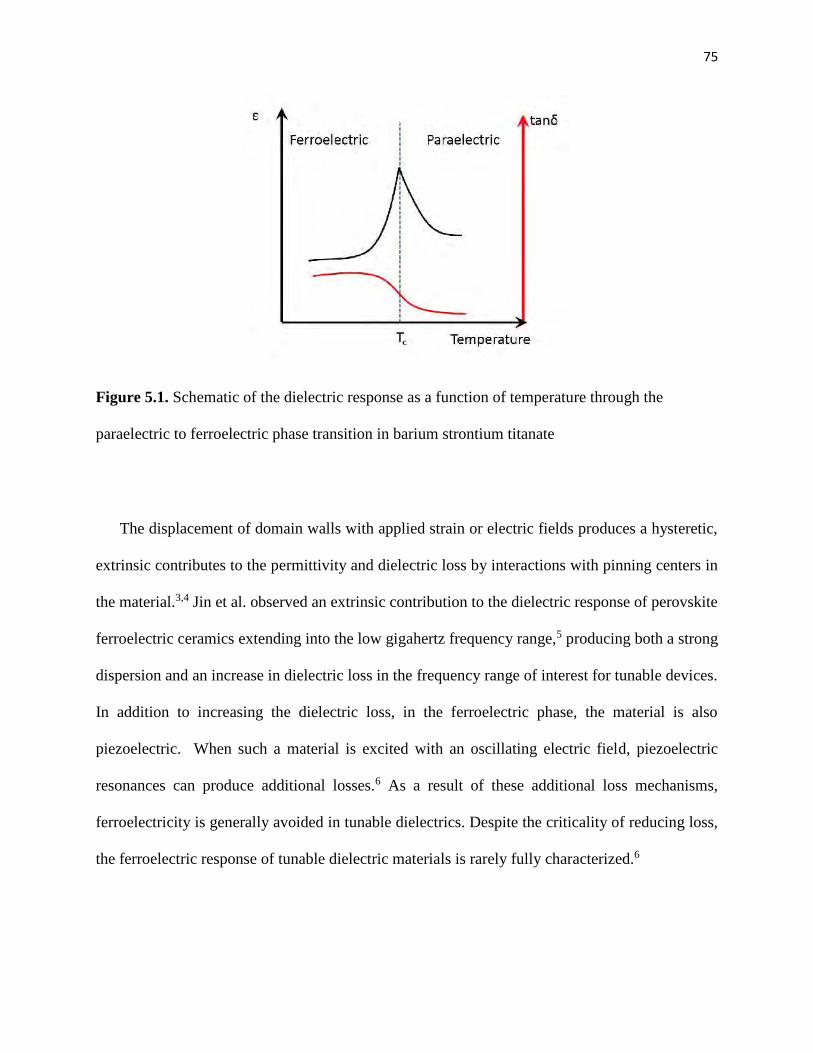
75
Figure 5.1. Schematic of the dielectric response as a function of temperature through the
paraelectric to ferroelectric phase transition in barium strontium titanate
The displacement of domain walls with applied strain or electric fields produces a hysteretic,
extrinsic contributes to the permittivity and dielectric loss by interactions with pinning centers in
the material.3,4 Jin et al. observed an extrinsic contribution to the dielectric response of perovskite
ferroelectric ceramics extending into the low gigahertz frequency range,5 producing both a strong
dispersion and an increase in dielectric loss in the frequency range of interest for tunable devices.
In addition to increasing the dielectric loss, in the ferroelectric phase, the material is also
piezoelectric. When such a material is excited with an oscillating electric field, piezoelectric
resonances can produce additional losses.6 As a result of these additional loss mechanisms,
ferroelectricity is generally avoided in tunable dielectrics. Despite the criticality of reducing loss,
the ferroelectric response of tunable dielectric materials is rarely fully characterized.6
76
The presence of residual ferroelectricity –a persistent ferroelectric response above the
macroscopic phase transition temperature –in tunable dielectrics, can be inferred from hysteresis
in the field dependence of the permittivity, piezoelectricity in the paraelectric phase, or excessive
dielectric loss.6,7,8,9,10 Direct measurements of this phenomena would provide a better
understanding of the prevalence, and origins (and thus routes to mitigation) of residual
ferroelectricity. A precedence for residual ferroelectricity has been established in barium titanate,
for which the existence of local polarization above the temperature of the displacive phase
transition is well documented.11,12,13,14 It has been reported that coalescence of the titanium ion
displacements along the <111> orientations leads to nanopolar-like regions, analogous to those
found in relaxor ferroelectrics.8,11,12 Anomalous birefringence, associated with local symmetry
breaking due to the titanium displacements, has been observed in bulk barium titanate single
crystals to persist 50°C above the global phase transition temperature, though models of elastic
coefficients predict the onset of nanopolar regions up to 75°C.13,15
These local structural distortions are not unique to barium titanate, but have been identified in
a range of materials which were considered to undergo exclusively displacive phase transitions to
the ferroelectric state.13 In barium strontium titanate, symmetry forbidden first-order Raman
scattering has been identified above the phase transition temperature.8,16,17 Forbidden scattering
modes, accompanied by soft-mode overdamping, have been ascribed to the strong coupling of the
nanopolar regions to the polar soft modes in relaxor ferroelectrics such as lead magnesium
niobate.18 Kim et al. observed significant increases in the microwave dielectric loss in well
crystallized samples correlated to the onset of local symmetry breaking in BST materials.17
However, the full temperature extent and impact to dielectric loss due of these order-disorder
derived nanopolar regions in BST has not been established.
77
In addition to intrinsic mechanisms, barium strontium titanate materials have the added
complication of many processing –or history –related sources for residual ferroelectricity in thin
films and bulk ceramics. Among the possibilities are chemical inhomogeneity,19,20,21 self-
polarization mechanisms due to injected or trapped charge,22,23,24 field-induced long range ordering
of local polar regions,25 local strain and local distortions due to doping, point defects or defect
dipoles.8,17,26,27,28 Chemical inhomogeneity on the A-site would produce areas rich in barium with
higher transition temperature than areas depleted of barium, leading to a diffuse phase transition.
Using confocal scanning optical microscopy to probe the local ferroelectric response across the
surface of chemical solution deposited BST thin films, Tikhomirov et al., observed 100°C variance
in the local ferroelectric transition temeprature.19 Additionally, substrate and processing induced
strain has been shown to shift or broaden the transition temperature in BST.1,29 While uniform
uniaxial strain, below the critical strain required to induce a phase transition, would not break the
symmetry of the system, strains due to defects could lead to regions of local ferroelectric distortion.
Local strains have been credited with the polar character along the grain boundaries of incipient
ferroelectric strontium titanate ceramics and oxygen vacancies have been implicated in appearance
of local polar response in STO and BST materials.22,26
This work describes the prevalence and temperature extent of residual ferroelectricity in
barium strontium titanate thin films as measured by Rayleigh analysis. Rayleigh analysis was used
to monitor the presence of domain walls (or other mobile interfaces, including the boundaries of
nanopolar regions) and the subsequent contribution to loss at temperatures above the global phase
transition temperature. Measurement of the dielectric temperature dependence and polarization-
electric field response are used to supplement and support the Rayleigh analysis and determine
possible origins of the residual ferroelectricity.
78
5.3. Sample Preparation
In this section, BST films from two different sources are discussed. Sputtered
(Ba0.7,Sr0.3)TiO3 thin films on polycrystalline alumina substrates were provided from Dr. Maria’s
group. The sputtered films employed interdigitated top electrodes, IDE, due to the degradation
which would occur to a platinum bottom electrode during the annealing of these films. The
dielectric response of these films is presented in capacitance. This is due to the increase in
uncertainty associated with the extraction of permittivity for these films from the Gevorgian IDE
calculations (due to variations in IDE arm thickness, spacing, and sample thickness).
Additionally (Ba0.8,Sr0.2)TiO3, (Ba0.7,Sr0.3)TiO3, (Ba0.6,Sr0.4)TiO3 thin films were deposited
by chemical solution deposition, CSD, onto platinized MgO. These samples employed a metal-
insulator-metal structures with platinum top electrodes.
5.4. Tunability
Figure 5.2 shows the characteristic tunability of the CSD BST thin films, taken at 25°C and
100 kHz. The relative tunability for the CSD (Ba0.8Sr0.2)TiO3, (Ba0.7Sr0.3)TiO3, (Ba0.6Sr0.4)TiO3, at
100 kHz, were characterized to fields over 250 kV/cm. The relative tunability and minimum
quality factor for the CSD BST films at 100 kHz is shown in table 5.1. At 1kHz the relative
tunability for the (Ba0.8Sr0.2)TiO3, (Ba0.7Sr0.3)TiO3 and (Ba0.6Sr0.4)TiO3 films are 90%, 86% and
72% and a dielectric loss of 0.0185, 0.005 and 0.002.
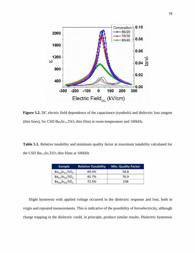
79
Figure 5.2. DC electric field dependence of the capacitance (symbols) and dielectric loss tangent
(thin lines), for CSD BaxSr1-xTiO3 thin films at room temperature and 100kHz.
Table 5.1. Relative tunability and minimum quality factor at maximum tunability calculated for
the CSD Ba1-xSrxTiO3 thin films at 100kHz
Slight hysteresis with applied voltage occurred in the dielectric response and loss, both in
virgin and repeated measurements. This is indicative of the possibility of ferroelectricity, although
charge trapping in the dielectric could, in principle, produce similar results. Dielectric hysteresis
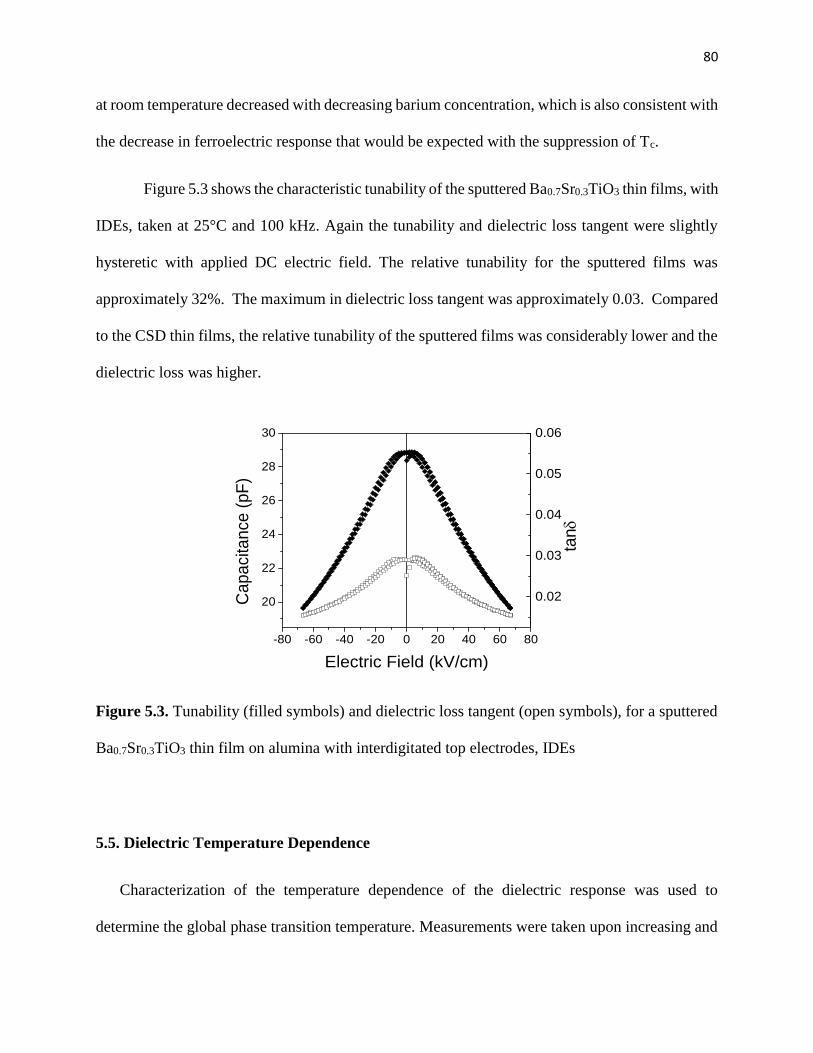
80
at room temperature decreased with decreasing barium concentration, which is also consistent with
the decrease in ferroelectric response that would be expected with the suppression of Tc.
Figure 5.3 shows the characteristic tunability of the sputtered Ba0.7Sr0.3TiO3 thin films, with
IDEs, taken at 25°C and 100 kHz. Again the tunability and dielectric loss tangent were slightly
hysteretic with applied DC electric field. The relative tunability for the sputtered films was
approximately 32%. The maximum in dielectric loss tangent was approximately 0.03. Compared
to the CSD thin films, the relative tunability of the sputtered films was considerably lower and the
dielectric loss was higher.
-80 -60 -40 -20 0 20 40 60 80
20
22
24
26
28
30
Cap
acita
nce
(pF)
Electric Field (kV/cm)
0.02
0.03
0.04
0.05
0.06
tan
Figure 5.3. Tunability (filled symbols) and dielectric loss tangent (open symbols), for a sputtered
Ba0.7Sr0.3TiO3 thin film on alumina with interdigitated top electrodes, IDEs
5.5. Dielectric Temperature Dependence
Characterization of the temperature dependence of the dielectric response was used to
determine the global phase transition temperature. Measurements were taken upon increasing and
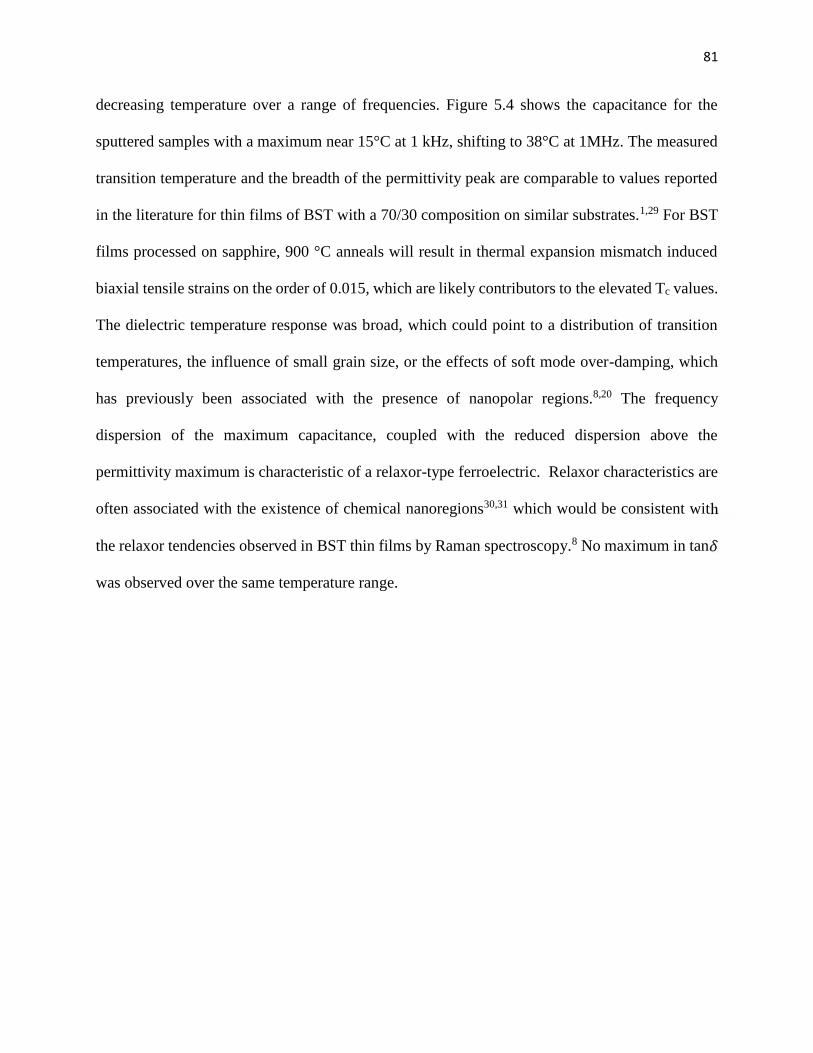
81
decreasing temperature over a range of frequencies. Figure 5.4 shows the capacitance for the
sputtered samples with a maximum near 15°C at 1 kHz, shifting to 38°C at 1MHz. The measured
transition temperature and the breadth of the permittivity peak are comparable to values reported
in the literature for thin films of BST with a 70/30 composition on similar substrates.1,29 For BST
films processed on sapphire, 900 °C anneals will result in thermal expansion mismatch induced
biaxial tensile strains on the order of 0.015, which are likely contributors to the elevated Tc values.
The dielectric temperature response was broad, which could point to a distribution of transition
temperatures, the influence of small grain size, or the effects of soft mode over-damping, which
has previously been associated with the presence of nanopolar regions.8,20 The frequency
dispersion of the maximum capacitance, coupled with the reduced dispersion above the
permittivity maximum is characteristic of a relaxor-type ferroelectric. Relaxor characteristics are
often associated with the existence of chemical nanoregions30,31 which would be consistent with
the relaxor tendencies observed in BST thin films by Raman spectroscopy.8 No maximum in tan
was observed over the same temperature range.
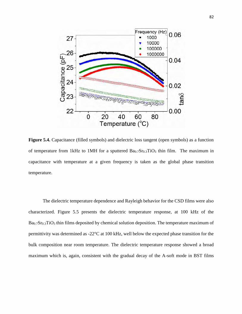
82
Figure 5.4. Capacitance (filled symbols) and dielectric loss tangent (open symbols) as a function
of temperature from 1kHz to 1MH for a sputtered Ba0.7Sr0.3TiO3 thin film. The maximum in
capacitance with temperature at a given frequency is taken as the global phase transition
temperature.
The dielectric temperature dependence and Rayleigh behavior for the CSD films were also
characterized. Figure 5.5 presents the dielectric temperature response, at 100 kHz of the
Ba0.7Sr0.3TiO3 thin films deposited by chemical solution deposition. The temperature maximum of
permittivity was determined as -22°C at 100 kHz, well below the expected phase transition for the
bulk composition near room temperature. The dielectric temperature response showed a broad
maximum which is, again, consistent with the gradual decay of the A-soft mode in BST films
83
determined by Raman spectroscopy.16 Similar to the sputtered films, frequency dispersion in the
maximum permittivity was also observed for all compositions of CSD thin films.
-50 -40 -30 -20 -10 0
1950
2000
2050
2100
2150
2200 Frequency (Hz)100100010000100000
Temperature (oC)
0.03
0.06
0.09
tan
Figure 5.5. Permittivity (filled symbols) and dielectric loss tangent (open symbols) as a function
of temperature from 100Hz to 1MH for a CSD Ba0.7Sr0.3TiO3 thin film with IDEs.
5.6. Temperature Dependence of Rayleigh Behavior
Figure 5.6-a presents characteristic measurements of capacitance as a function of the AC
electric field for sputtered BST films, at 1MHz. Data were acquired from 90 to 10°C on cooling
through the paraelectric to ferroelectric phase transition determined from the dielectric temperature
dependence. The applied electric field was limited to 15 kV/cm. Both capacitance and loss tangent
increased linearly with the applied AC electric field over this field range for all temperatures
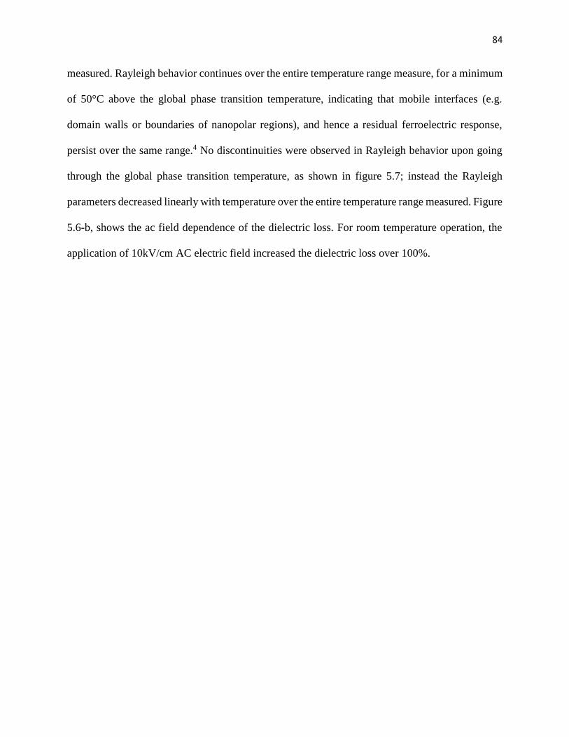
84
measured. Rayleigh behavior continues over the entire temperature range measure, for a minimum
of 50°C above the global phase transition temperature, indicating that mobile interfaces (e.g.
domain walls or boundaries of nanopolar regions), and hence a residual ferroelectric response,
persist over the same range.4 No discontinuities were observed in Rayleigh behavior upon going
through the global phase transition temperature, as shown in figure 5.7; instead the Rayleigh
parameters decreased linearly with temperature over the entire temperature range measured. Figure
5.6-b, shows the ac field dependence of the dielectric loss. For room temperature operation, the
application of 10kV/cm AC electric field increased the dielectric loss over 100%.
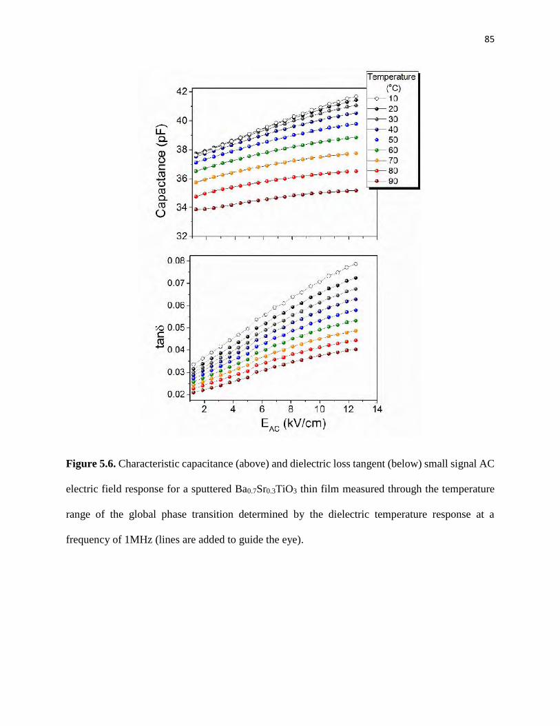
85
Figure 5.6. Characteristic capacitance (above) and dielectric loss tangent (below) small signal AC
electric field response for a sputtered Ba0.7Sr0.3TiO3 thin film measured through the temperature
range of the global phase transition determined by the dielectric temperature response at a
frequency of 1MHz (lines are added to guide the eye).
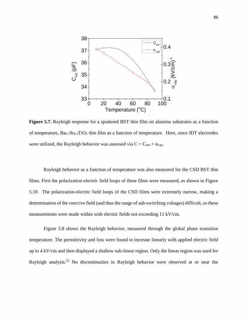
86
33
34
35
36
37
38
Cin
it (pF
)
Temperature (oC)
Cinit
cap
0 20 40 60 80 1000.1
0.2
0.3
0.4
ca
p (kV
/cm
)-1
Figure 5.7. Rayleigh response for a sputtered BST thin film on alumina substrates as a function
of temperature, Ba0.7Sr0.3TiO3 thin film as a function of temperature. Here, since IDT electrodes
were utilized, the Rayleigh behavior was assessed via C = Cinit + αcap.
Rayleigh behavior as a function of temperature was also measured for the CSD BST thin
films. First the polarization-electric field loops of these films were measured, as shown in Figure
5.10. The polarization-electric field loops of the CSD films were extremely narrow, making a
determination of the coercive field (and thus the range of sub-switching voltages) difficult, so these
measurements were made within with electric fields not exceeding 11 kV/cm.
Figure 5.8 shows the Rayleigh behavior, measured through the global phase transition
temperature. The permittivity and loss were found to increase linearly with applied electric field
up to 4 kV/cm and then displayed a shallow sub-linear region. Only the linear region was used for
Rayleigh analysis.32 No discontinuities in Rayleigh behavior were observed at or near the
87
temperature of maximum permittivity, with the Rayleigh response decreasing with increasing
temperature, until disappearing completely at 44°C for the measurement conditions employed.
Figure 5.8. Characteristic permittivity (above) and dielectric loss (below) as a function of AC
electric field response for a CSD Ba0.7Sr0.3TiO3 thin film with a global phase transition temperature
of -22°C at 100 kHz
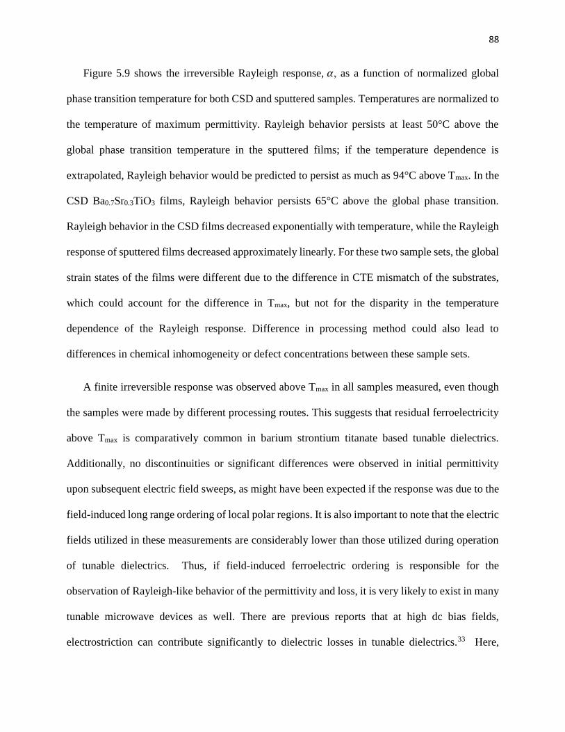
88
Figure 5.9 shows the irreversible Rayleigh response, , as a function of normalized global
phase transition temperature for both CSD and sputtered samples. Temperatures are normalized to
the temperature of maximum permittivity. Rayleigh behavior persists at least 50°C above the
global phase transition temperature in the sputtered films; if the temperature dependence is
extrapolated, Rayleigh behavior would be predicted to persist as much as 94°C above Tmax. In the
CSD Ba0.7Sr0.3TiO3 films, Rayleigh behavior persists 65°C above the global phase transition.
Rayleigh behavior in the CSD films decreased exponentially with temperature, while the Rayleigh
response of sputtered films decreased approximately linearly. For these two sample sets, the global
strain states of the films were different due to the difference in CTE mismatch of the substrates,
which could account for the difference in Tmax, but not for the disparity in the temperature
dependence of the Rayleigh response. Difference in processing method could also lead to
differences in chemical inhomogeneity or defect concentrations between these sample sets.
A finite irreversible response was observed above Tmax in all samples measured, even though
the samples were made by different processing routes. This suggests that residual ferroelectricity
above Tmax is comparatively common in barium strontium titanate based tunable dielectrics.
Additionally, no discontinuities or significant differences were observed in initial permittivity
upon subsequent electric field sweeps, as might have been expected if the response was due to the
field-induced long range ordering of local polar regions. It is also important to note that the electric
fields utilized in these measurements are considerably lower than those utilized during operation
of tunable dielectrics. Thus, if field-induced ferroelectric ordering is responsible for the
observation of Rayleigh-like behavior of the permittivity and loss, it is very likely to exist in many
tunable microwave devices as well. There are previous reports that at high dc bias fields,
electrostriction can contribute significantly to dielectric losses in tunable dielectrics.33 Here,
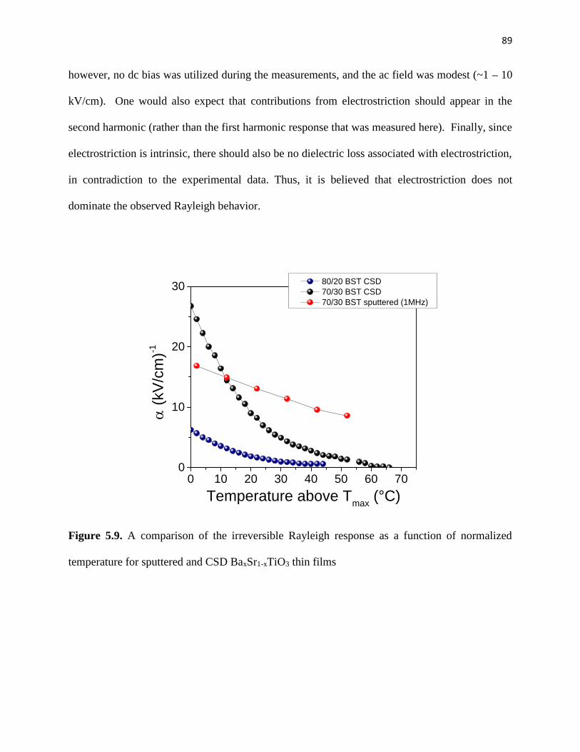
89
however, no dc bias was utilized during the measurements, and the ac field was modest (~1 – 10
kV/cm). One would also expect that contributions from electrostriction should appear in the
second harmonic (rather than the first harmonic response that was measured here). Finally, since
electrostriction is intrinsic, there should also be no dielectric loss associated with electrostriction,
in contradiction to the experimental data. Thus, it is believed that electrostriction does not
dominate the observed Rayleigh behavior.
0 10 20 30 40 50 60 700
10
20
30 80/20 BST CSD 70/30 BST CSD 70/30 BST sputtered (1MHz)
(k
V/cm
)-1
Temperature above Tmax (°C)
Figure 5.9. A comparison of the irreversible Rayleigh response as a function of normalized
temperature for sputtered and CSD BaxSr1-xTiO3 thin films
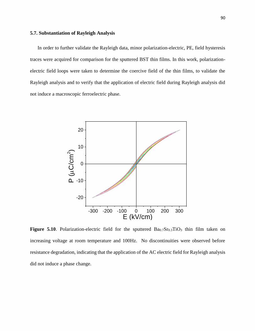
90
5.7. Substantiation of Rayleigh Analysis
In order to further validate the Rayleigh data, minor polarization-electric, PE, field hysteresis
traces were acquired for comparison for the sputtered BST thin films. In this work, polarization-
electric field loops were taken to determine the coercive field of the thin films, to validate the
Rayleigh analysis and to verify that the application of electric field during Rayleigh analysis did
not induce a macroscopic ferroelectric phase.
-300 -200 -100 0 100 200 300
-20
-10
0
10
20
P (
C/c
m2 )
E (kV/cm)Figure 5.10. Polarization-electric field for the sputtered Ba0.7Sr0.3TiO3 thin film taken on
increasing voltage at room temperature and 100Hz. No discontinuities were observed before
resistance degradation, indicating that the application of the AC electric field for Rayleigh analysis
did not induce a phase change.
91
Figure 5.11. Polarization electric field loops for the CSD Ba0.7Sr0.3TiO3 thin film taken at room
temperature. b.(inset) Magnification showing the remanent polarization and the coercive electric
field. P-E loops were extremely slim, indicating the materials were likely macroscopically
paraelectric at room temperature.
Polarization-electric field loops for the CSD and sputtered films are shown in Figure 5.10 and
5.11. P-E loops were taken upon increasing the applied electric field and are an average of ten
measurements per electric field step. The average coercive field and remanent polarization
measured at the maximum field for the sputtered films were were 15 kV/cm and 1.75 µC/cm2
respectively. Over this field range, there were no discontinuities in the polarization as would be
observed for an electric field induced ferroelectric phase transition. This supports that assumption
the measured Rayleigh response is due to the movement of preexisting domain walls or boundaries
of nanopolar regions. Minor P-E hysteresis traces were also calculated from the Rayleigh data as
follows:
-300 -200 -100 0 100 200 300-15
-10
-5
0
5
10
15
Pola
rizat
ion
(C
/cm
2 )
Electric Field (kV/cm)
-20 -10 0 10 20-1.5-1.0-0.50.00.51.01.5
Pola
rizat
ion
(C
/cm
2 )
Electric Field (kV/cm)
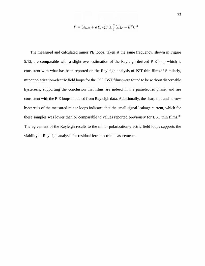
92
= ( + ) ± ( − ).34
The measured and calculated minor PE loops, taken at the same frequency, shown in Figure
5.12, are comparable with a slight over estimation of the Rayleigh derived P-E loop which is
consistent with what has been reported on the Rayleigh analysis of PZT thin films.34 Similarly,
minor polarization-electric field loops for the CSD BST films were found to be without discernable
hysteresis, supporting the conclusion that films are indeed in the paraelectric phase, and are
consistent with the P-E loops modeled from Rayleigh data. Additionally, the sharp tips and narrow
hysteresis of the measured minor loops indicates that the small signal leakage current, which for
these samples was lower than or comparable to values reported previously for BST thin films.35
The agreement of the Rayleigh results to the minor polarization-electric field loops supports the
viability of Rayleigh analysis for residual ferroelectric measurements.
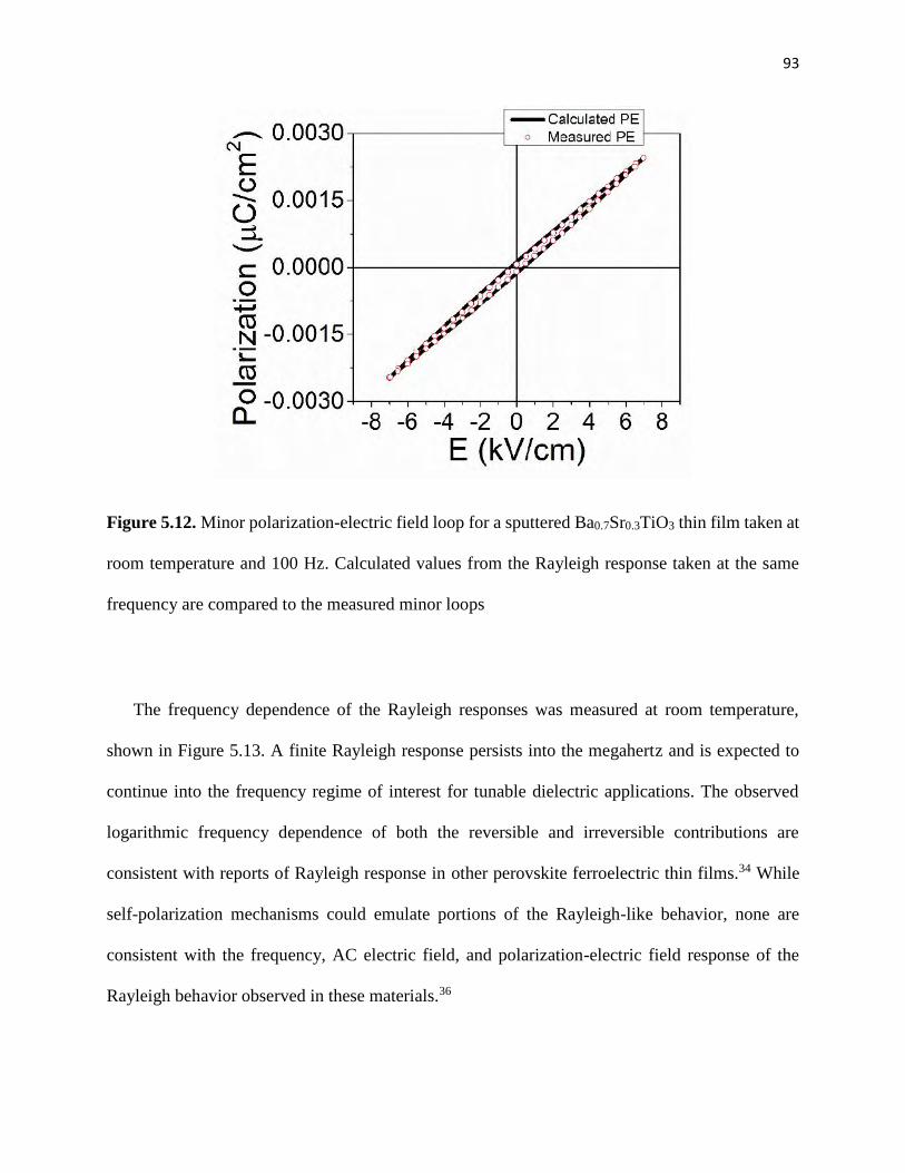
93
Figure 5.12. Minor polarization-electric field loop for a sputtered Ba0.7Sr0.3TiO3 thin film taken at
room temperature and 100 Hz. Calculated values from the Rayleigh response taken at the same
frequency are compared to the measured minor loops
The frequency dependence of the Rayleigh responses was measured at room temperature,
shown in Figure 5.13. A finite Rayleigh response persists into the megahertz and is expected to
continue into the frequency regime of interest for tunable dielectric applications. The observed
logarithmic frequency dependence of both the reversible and irreversible contributions are
consistent with reports of Rayleigh response in other perovskite ferroelectric thin films.34 While
self-polarization mechanisms could emulate portions of the Rayleigh-like behavior, none are
consistent with the frequency, AC electric field, and polarization-electric field response of the
Rayleigh behavior observed in these materials.36
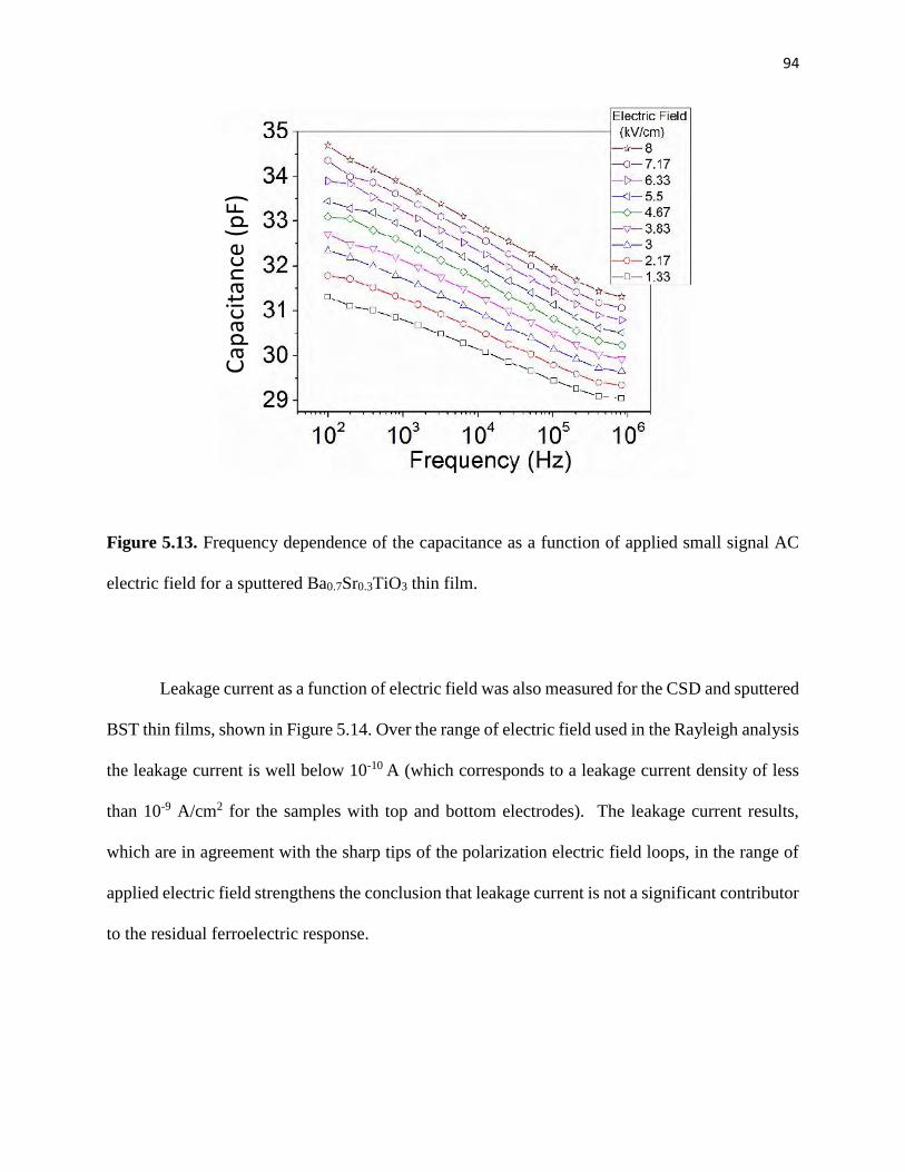
94
Figure 5.13. Frequency dependence of the capacitance as a function of applied small signal AC
electric field for a sputtered Ba0.7Sr0.3TiO3 thin film.
Leakage current as a function of electric field was also measured for the CSD and sputtered
BST thin films, shown in Figure 5.14. Over the range of electric field used in the Rayleigh analysis
the leakage current is well below 10-10 A (which corresponds to a leakage current density of less
than 10-9 A/cm2 for the samples with top and bottom electrodes). The leakage current results,
which are in agreement with the sharp tips of the polarization electric field loops, in the range of
applied electric field strengthens the conclusion that leakage current is not a significant contributor
to the residual ferroelectric response.
Capa
citan
ce (p
F)
95
0 10 20 30 40 50 60 70 80 90 1000
1x10⁻¹⁰
2x10⁻¹⁰
3x10⁻¹⁰
4x10⁻¹⁰
5x10⁻¹⁰
6x10⁻¹⁰
Leak
age
Cur
rent
(A)
Electric Field (kV/cm)
CSD BST Sputtered BST
Figure 5.14. Leakage current for the CSD and sputtered BST thin films
In the next chapter the impact of chemical inhomogeneity on the presence of residual
ferroelectricity and relaxor ferroelectric characteristics is discussed for barium strontium titanate
thin films and ceramics. It is clear that residual ferroelectricity is observed in films prepared by
completely different routes (and hence with different processing defects). The implications of the
observed temperature extent of the measured Rayleigh response in the sputtered and CSD thin
films is that complete removal of the ferroelectric contributions to loss would require the
suppression of Tmax well below room temperature in addition to well- controlled processing.
Ferroelectric measurements become more relevant as the ratio of barium to strontium pushes the
phase transition temperature of the BST solid solution closer to room temperature. While
processing defects, such as point defects, local strain or self-polarization mechanisms, do
contribute to the dielectric loss of these materials, defects alone could not account for the observed
frequency and temperature dependence of the residual ferroelectricity. It should be stressed that
96
the electric field range used in Rayleigh analysis are well below those the material will experience
in operation, making ferroelectric measurements under operation conditions critical. Moreover,
the prevalence of residual ferroelectricity highlights the importance of ferroelectric measurements
in understanding and mitigating loss in tunable dielectrics. Additionally, the prevalence of residual
ferroelectricity suggests that comparable measurements should be made in similar perovskite
materials, especially those with coexistent order-disorder and displacive phase transition
characteristics.
5.8. Conclusions
In conclusion, residual ferroelectricity in (Ba1-x,Srx)TiO3 thin films was identified and
characterized by Rayleigh analysis. Measurements of Rayleigh response as a function of
temperature determined that residual ferroelectricity in the sputtered and CSD thin films persisted
at least 50°C and 65°C respectively above the global transition temperature determined from the
capacitive temperature response. Frequency dispersion in the dielectric temperature response
points towards the presence of nanopolar regions as one source of residual ferroelectricity. The
Rayleigh behavior was found to be consistent with the minor polarization-electric field loops.
5.9. References
1. Tagantsev, A. K., Sherman, V. O., Astafiev, K. F., Venkatesh, J. & Setter, N. Ferroelectric
materials for microwave tunable applications. J. Electroceramics 11, 5–66 (2003).
97
2. York, R.A. , “Tunable Dielectrics for RF Circuits”, Multifunctional Adaptive Microwave
Circuits and Systems, M. Steer, W. D. Palmer (Editors), SciTech Publishing, (2009).
3. Damjanovic, D. Hysteresis in piezoelectric and ferroelectric materials. The science of
hysteresis, 3, 337-465. (2006).
4. D. V. Taylor. Dielectric and Piezoelectric Properties of Sol-Gel Derived PZT Thin Films.
Ph.D. dissertation, EPFL (1999).
5. Jin, L., Porokhonskyy, V. & Damjanovic, D. Domain wall contributions in Pb(Zr,Ti)O3
ceramics at morphotropic phase boundary: A study of dielectric dispersion. Appl. Phys. Lett.
96, 242902–242902–3 (2010).
6. Gevorgian, S. S. & Kollberg, E. L. Do we really need ferroelectrics in paraelectric phase only
in electrically controlled microwave devices? IEEE Trans. Microw. Theory Tech. 49, 2117–
2124 (2001).
7. Vendik, O. G., Hollmann, E. K., Kozyrev, A. B. & Prudan, A. M. Ferroelectric tuning of
planar and bulk microwave devices. J. Supercond. 12, 325–338 (1999).
8. A. Soukiassian D. A. Tenne. Raman study of BaxSr1-xTiO3 films: Evidence for the existence
of polar nanoregions. Phys. Rev. B 67, 1, 012302 (2003).
9. Nath, R., Zhong, S., Alpay, S. P., Huey, B. D. & Cole, M. W. Enhanced piezoelectric
response from barium strontium titanate multilayer films. Appl. Phys. Lett. 92, 012916–3
(2008).
10. Fu, C., Yang, C., Domain configuration and dielectric properties of Ba0.6Sr0.4TiO3 thin films.
Appl. Surf. Sci.252, 461–465 (2005).
11. Zalar, B., Laguta, V. V. & Blinc, R. NMR Evidence for the coexistence of order-disorder and
displacive components in barium titanate. Phys. Rev. Lett. 90, 037601 (2003).
98
12. Blinc, R., Advanced Ferroelectricity. Oxford Science Publications, 151, (2011).
13. Bussmann-Holder, A., Beige, H. & Völkel, G. Precursor effects, broken local symmetry, and
coexistence of order-disorder and displacive dynamics in perovskite ferroelectrics. Phys. Rev.
B 79, 184111 (2009).
14. Petkov, V., Gateshki, M., Niederberger, M. & Ren, Y. Atomic-Scale structure of
nanocrystalline BaxSr1-xTiO3 (x = 1, 0.5, 0) by x-ray diffraction and the atomic pair
distribution function technique. Chem. Mater. 18, 814–821 (2006).
15. Ko, J.-H., Kim, T. H., Roleder, K., Rytz, D. & Kojima, S. Precursor dynamics in the
ferroelectric phase transition of barium titanate single crystals studied by Brillouin light
scattering. Phys. Rev. B 84, 094123 (2011).
17. Tenne, D. A. et al. Lattice dynamics in BaxSr1−xTiO3 thin films studied by Raman
spectroscopy. J. Appl. Phys. 96, 6597–6605 (2004).
18. Tae-Gon Kim, J. O. Effect of crystallinity on the dielectric loss of sputter-deposited
(Ba,Sr)TiO3 thin films in the microwave range. J. Mater. Res. 18, 682 – 686 (2003).
18. Wakimoto, S., Stock, C., Birgeneau, R. J., Ye, Z.-G. Chen, W., Buyers, W. J. L., Gehring, P.
M. and Shirane, G. Ferroelectric ordering in the relaxor Pb(Mg1/3Nb2/3)O3 as evidenced by
low-temperature phonon anomalies. Phys. Rev. B 65, 172105 (2002).
19. Tikhomirov, O., Jiang, H. & Levy, J. Direct observation of local ferroelectric phase
transitions in BaxSr1−xTiO3 thin films. Appl. Phys. Lett. 77, 2048–2050 (2000).
20. Li, S., Eastman, J. A., Newnham, R. E. & Cross, L. E. Diffuse phase transition in
ferroelectrics with mesoscopic heterogeneity: Mean-field theory. Phys. Rev. B 55, 73831–
12078 (1997).
99
21. Pervez, N. K., Hansen, P. J. & York, R. A. High tunability barium strontium titanate thin
films for rf circuit applications. Appl. Phys. Lett. 85, 4451–4453 (2004).
22. Chynoweth, A. G. Surface space-charge layers in barium titanate. Phys. Rev. 102, 705–714
(1956).
23. Peng, C.-J. & Krupanidhi, S. B. Structures and electrical properties of barium strontium
titanate thin films grown by multi-ion-beam reactive sputtering technique. J. Mater. Res. 10,
708–726 (1995).
24. Pontes, F. M., Liete, E. R., Longo, E., Varela, J. A., and Eiras, J. A. Effects of the
postannealing atmosphere on the dielectric properties of (Ba, Sr)TiO3 capacitors: Evidence of
an interfacial space charge layer. Appl. Phys. Lett. 76, 2433–2435 (2000).
25. Lookman, A., McAeney, J., Bowman, R. M., Gregg, J. M., Kut, J., Rios, S., Ruediger, A.,
Dawber, M., Scott, J. F. Effects of poling, and implications for metastable phase behavior in
barium strontium titanate thin film capacitors. Appl. Phys. Lett. 85, 5010 (2004).
26. Pertsev, N. A., Tagantsev, A. K. & Setter, N. Phase transitions and strain-induced
ferroelectricity in SrTiO3 epitaxial thin films. Phys. Rev. B 61, R825–R829 (2000).
27. Hyun, S. et al., Effects of strain on the dielectric properties of tunable dielectric SrTiO3 thin
films. Appl. Phys. Lett. 79, (2001).
28. Herner, S. B., Selmi, F. A., Varadan, V. V. & Varadan, V. K. The effect of various dopants
on the dielectric properties of barium strontium titanate. Mater. Lett. 15, 317–324 (1993).
29. Ito, S., Funakubo, H., Koutsaroff, I. P., Zelner, M. and Cervin-Lawry, A. Effect of the
thermal expansion matching on the dielectric tunability of (100)-one-axis-oriented
(Ba0.5Sr0.5)TiO3 thin films. Appl. Phys. Lett. 90, 142910–3 (2007).
100
30. Davies, P., and Akbas, M., Chemical order in PMN-related relaxors: structure, stability,
modification, and impact on properties. J. Phys. Chem. Solids 61, 159–166 (2000).
31. Randall, C. A., Barber, D. J., Groves, P., and Whatmore, R. W. TEM study of the disorder-
order perovskite, Pb(In1/2Nb1/2)O3. J. Mater. Sci. 23, 3678–3682 (1988).
32. Bassiri Gharb, N., Dielectric and Piezoelectric Nonlinearities in Oriented Pb(Yb1/2Nb1/2)O3-
PbTiO3 Thin Films. Ph.D. dissertation, Dept. of Mat. Sci and Eng., Penn. State University,
University Park, PA, 2005.
33. Tappe, S., Bottger, U., and Waser, R. Electrostrictive resonances in (Ba0.7Sr0.3)TiO3 thin
films at microwave frequencies. Appl. Phys. Lett. 85, 624–626 (2004).
34. Taylor, D. V., and Damjanovic, D. Evidence of domain wall contribution to the dielectric
permittivity in PZT thin films at sub-switching fields. J. Appl. Phys. 82, 1973–1975 (1997).
35. Zafar, S., Jones, R. E., Jiang, B., White, B., Kaushik, V., Gillespie, S.The electronic
conduction mechanism in barium strontium titanate thin films. Appl. Phys. Lett. 73, 3533–
3535 (1998).
36. Afanas’ev, V. P., Pronin, I. P. & Kholkin, A. L. Formation and relaxation mechanisms of the
self-polarization in thin ferroelectric films. Phys. Solid State 48, 1214–1218 (2006).
101
Chapter 6
Further Evidence for Residual Ferroelectricity in BST
6.1. Introduction
Barium strontium titanate is the primary candidate for tunable dielectric applications but
suffers decreased performance due to high dielectric loss.1 Reducing this loss requires an
understanding of the ferroelectric and dielectric factors leading to increased loss.
In the previous chapter, the presence of residual ferroelectricity in BST thin films was
presented. This chapter expands upon these findings and presents data on the residual ferroelectric
response for a series of thin films and ceramics. Nano-scale polar clusters, and nano-scale chemical
inhomogeneity are characterized and discussed as underlying mechanisms contributing to the
observed residual ferroelectric response.
Relaxor ferrroelectricity has previously been suggested to occur in barium strontium
titanate, as evidenced by disallowed first order phonon peaks in Raman spectroscopy.2
Additionally, frequency dispersion which collapses above Tmax has previously been reported in
40:60 BST ceramics, as shown in Figure 6.1. Zhou et al. investigated the impact of the pre-
calcination mixing time on the dielectric temperature response.3 It was noted that with decreasing
mixing, and one would infer increasing chemical heterogeneity, frequency dispersion appeared in
the dielectric response. It is possible that relaxor-like ferroelectric behavior is related to the residual
ferroelectricity observed in this study.
102
Figure 6.1. Ba0.4Sr0.6TiO3 ceramics with different pre-calcination mixing times a.) 0 hours, b.) 3
hours, c.) 6 hours, and d.) 9 hours3. The amount of dielectric dispersion characteristic of relaxor
ferroelectric characteristics is larger for shorter mixing times.
A series of experimental techniques, including second harmonic generation was employed here
to determine the presence of nano-scale polar clusters in barium strontium titanate films and
ceramics, and to investigate the impact of chemical inhomogeneity on the development of relaxor
behavior in BST. The development of relaxor behavior is also discussed in the context of variations
in chemical inhomogeneity as observed through electron energy loss spectroscopy.
103
6.2. Methods
Film deposition conditions and sample preparation for films produced by chemical solution
deposited, CSD, and radio frequency-magnetron sputtered are discussed in chapter 3 and provided
in reference 4. The sputter deposited BST thin films employed platinum interdigitated electrodes,
while the CSD films had a metal-insulator-metal electrode structure with platinum top and bottom
electrodes. The ceramic samples used in this investigation had approximate compositions of
Ba0.7Sr0.3TiO3 and Ba0.67Sr0.33TiO3 and were fabricated by Texas Instruments using a wet chemical
approach with strict tolerances on the level of chemical inhomogeneity.5
6.3 Results
6.3.1. Dielectric Temperature Response
Figure 6.2 provides the temperature dependence of the dielectric response of the
Ba0.8Sr0.2TiO3 (80:20) chemical solution deposited thin films. The maximum in the dielectric
response was taken as the transition from the paraelectric to ferroelectric phase. The broad
maximum observed in the CSD 80:20 BST thin films is characteristic of the response seen in all
of the measured thin films. The frequency dispersion in the dielectric temperature response, along
with the reduced dispersion above Tmax is indicative of relaxor ferroelectric behavior.6 Data for
sputtered and CSD films are shown in chapter 5.
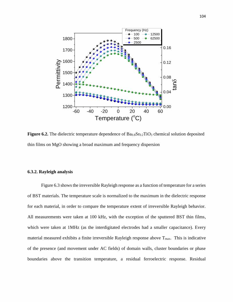
104
-60 -40 -20 0 20 40 601200
1300
1400
1500
1600
1700
1800
Perm
ittiv
ity
Temperature (oC)
Frequency (Hz)100 12500500 625002500
0.00
0.04
0.08
0.12
0.16
tan
Figure 6.2. The dielectric temperature dependence of Ba0.8Sr0.2TiO3 chemical solution deposited
thin films on MgO showing a broad maximum and frequency dispersion
6.3.2. Rayleigh analysis
Figure 6.3 shows the irreversible Rayleigh response as a function of temperature for a series
of BST materials. The temperature scale is normalized to the maximum in the dielectric response
for each material, in order to compare the temperature extent of irreversible Rayleigh behavior.
All measurements were taken at 100 kHz, with the exception of the sputtered BST thin films,
which were taken at 1MHz (as the interdigitated electrodes had a smaller capacitance). Every
material measured exhibits a finite irreversible Rayleigh response above Tmax. This is indicative
of the presence (and movement under AC fields) of domain walls, cluster boundaries or phase
boundaries above the transition temperature, a residual ferroelectric response. Residual
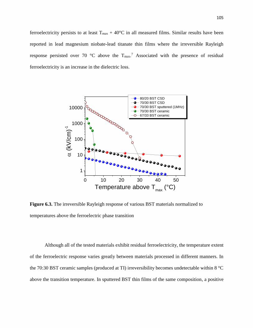
105
ferroelectricity persists to at least Tmax + 40°C in all measured films. Similar results have been
reported in lead magnesium niobate-lead titanate thin films where the irreversible Rayleigh
response persisted over 70 °C above the Tmax.7 Associated with the presence of residual
ferroelectricity is an increase in the dielectric loss.
0 10 20 30 40 50
1
10
100
1000
10000
(k
V/cm
)-1
Temperature above Tmax (°C)
80/20 BST CSD 70/30 BST CSD 70/30 BST sputtered (1MHz) 70/30 BST ceramic 67/33 BST ceramic
Figure 6.3. The irreversible Rayleigh response of various BST materials normalized to
temperatures above the ferroelectric phase transition
Although all of the tested materials exhibit residual ferroelectricity, the temperature extent
of the ferroelectric response varies greatly between materials processed in different manners. In
the 70:30 BST ceramic samples (produced at TI) irreversibility becomes undetectable within 8 °C
above the transition temperature. In sputtered BST thin films of the same composition, a positive
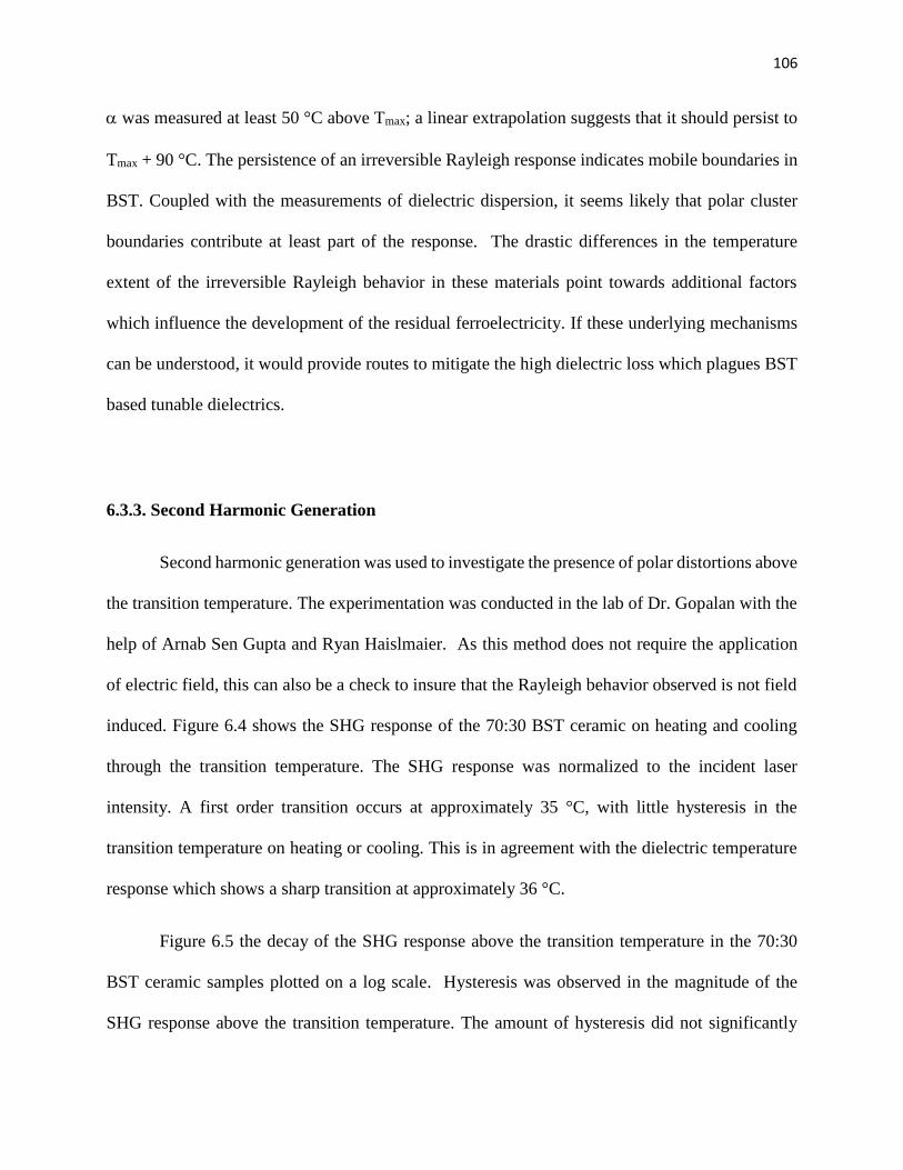
106
was measured at least 50 °C above Tmax; a linear extrapolation suggests that it should persist to
Tmax + 90 °C. The persistence of an irreversible Rayleigh response indicates mobile boundaries in
BST. Coupled with the measurements of dielectric dispersion, it seems likely that polar cluster
boundaries contribute at least part of the response. The drastic differences in the temperature
extent of the irreversible Rayleigh behavior in these materials point towards additional factors
which influence the development of the residual ferroelectricity. If these underlying mechanisms
can be understood, it would provide routes to mitigate the high dielectric loss which plagues BST
based tunable dielectrics.
6.3.3. Second Harmonic Generation
Second harmonic generation was used to investigate the presence of polar distortions above
the transition temperature. The experimentation was conducted in the lab of Dr. Gopalan with the
help of Arnab Sen Gupta and Ryan Haislmaier. As this method does not require the application
of electric field, this can also be a check to insure that the Rayleigh behavior observed is not field
induced. Figure 6.4 shows the SHG response of the 70:30 BST ceramic on heating and cooling
through the transition temperature. The SHG response was normalized to the incident laser
intensity. A first order transition occurs at approximately 35 °C, with little hysteresis in the
transition temperature on heating or cooling. This is in agreement with the dielectric temperature
response which shows a sharp transition at approximately 36 °C.
Figure 6.5 the decay of the SHG response above the transition temperature in the 70:30
BST ceramic samples plotted on a log scale. Hysteresis was observed in the magnitude of the
SHG response above the transition temperature. The amount of hysteresis did not significantly
107
change with the ramp rates from 1-6 °C/min. At approximately 190 °C there is a change in the
slope of the SHG response. It is possible that this indicates the Burns temperature, although other
authors suggest that TBurns is closer to 100 °C above Tmax (e.g. ~ 130°C in this case).12 There are
no other likely structural or electrical transitions within this temperature regime. A second
possibility is that the change in slope could be due to oxygen vacancies or vacancy cluster
movement.13 Near 250 °C the hysteresis in the response on heating and cooling collapses. The
SHG response continues to decrease in a linear fashion until hitting a noise floor at approximately
440 °C. A finite noise floor above that determined by the SHG equipment is expected in all
measured samples due to the symmetry breaking at the grain boundaries.
0 100 200 300 4000
500
1000
1500
2000
Nor
mal
ized
SH
G (a
rb. u
nits
)
Temperature (°C)
Ramp Rate 3°/min 6°/min
Figure 6.4. Normalized SHG response from the 70:30 BST ceramic samples taken at a ramp rate
of 3 °C/min and 6 °C/min
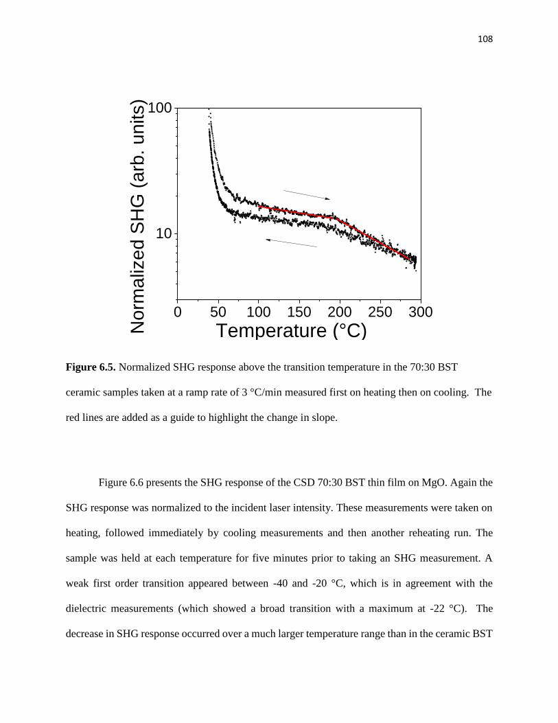
108
0 50 100 150 200 250 300
10
100
Nor
mal
ized
SH
G (a
rb. u
nits
)
Temperature (°C)
Figure 6.5. Normalized SHG response above the transition temperature in the 70:30 BST
ceramic samples taken at a ramp rate of 3 °C/min measured first on heating then on cooling. The
red lines are added as a guide to highlight the change in slope.
Figure 6.6 presents the SHG response of the CSD 70:30 BST thin film on MgO. Again the
SHG response was normalized to the incident laser intensity. These measurements were taken on
heating, followed immediately by cooling measurements and then another reheating run. The
sample was held at each temperature for five minutes prior to taking an SHG measurement. A
weak first order transition appeared between -40 and -20 °C, which is in agreement with the
dielectric measurements (which showed a broad transition with a maximum at -22 °C). The
decrease in SHG response occurred over a much larger temperature range than in the ceramic BST
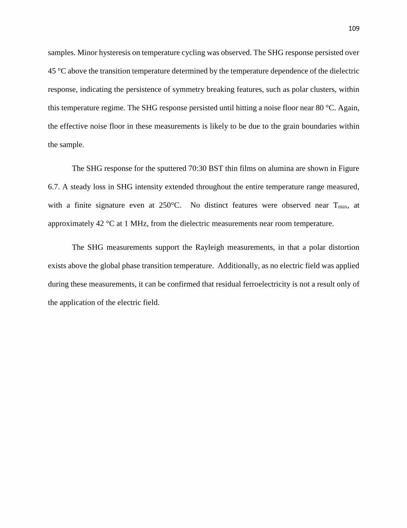
109
samples. Minor hysteresis on temperature cycling was observed. The SHG response persisted over
45 °C above the transition temperature determined by the temperature dependence of the dielectric
response, indicating the persistence of symmetry breaking features, such as polar clusters, within
this temperature regime. The SHG response persisted until hitting a noise floor near 80 °C. Again,
the effective noise floor in these measurements is likely to be due to the grain boundaries within
the sample.
The SHG response for the sputtered 70:30 BST thin films on alumina are shown in Figure
6.7. A steady loss in SHG intensity extended throughout the entire temperature range measured,
with a finite signature even at 250°C. No distinct features were observed near Tmax, at
approximately 42 °C at 1 MHz, from the dielectric measurements near room temperature.
The SHG measurements support the Rayleigh measurements, in that a polar distortion
exists above the global phase transition temperature. Additionally, as no electric field was applied
during these measurements, it can be confirmed that residual ferroelectricity is not a result only of
the application of the electric field.
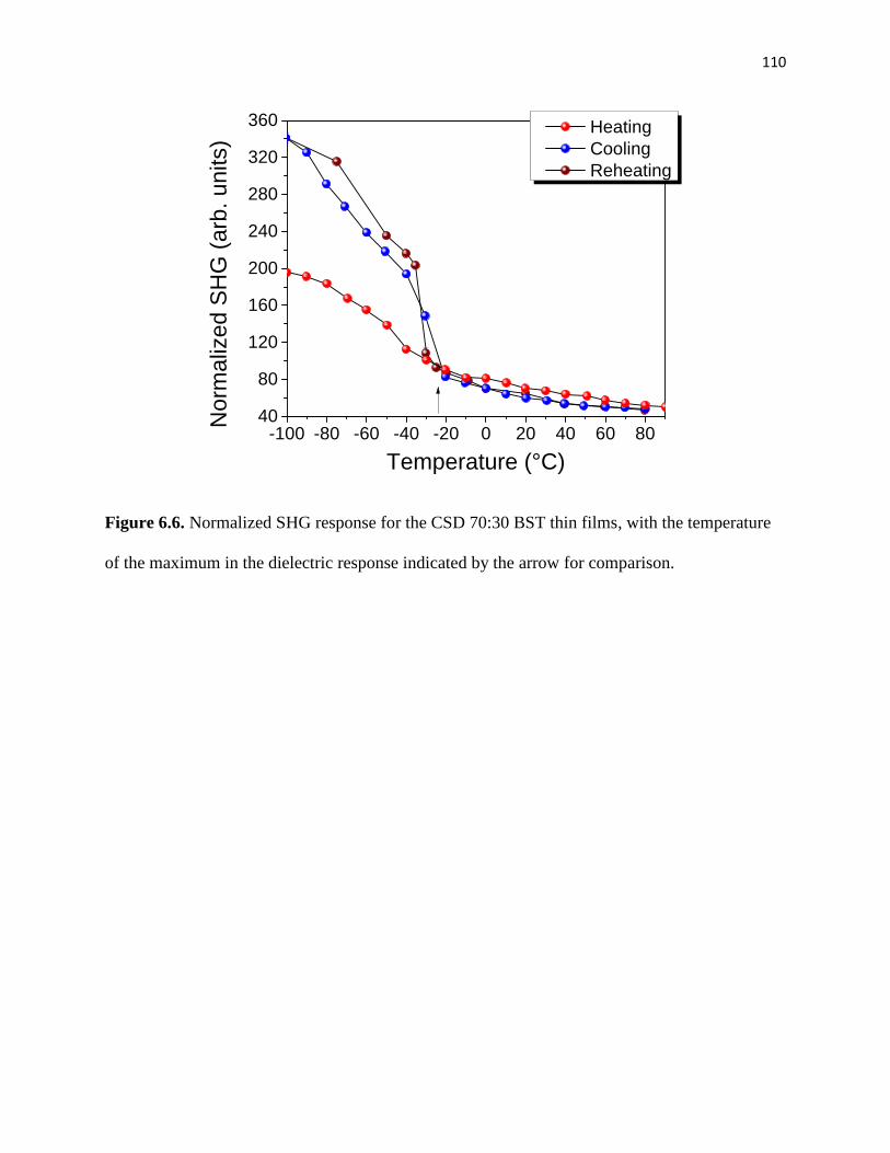
110
-100 -80 -60 -40 -20 0 20 40 60 8040
80
120
160
200
240
280
320
360
Nor
mal
ized
SH
G (a
rb. u
nits
)
Temperature (°C)
Heating Cooling Reheating
Figure 6.6. Normalized SHG response for the CSD 70:30 BST thin films, with the temperature
of the maximum in the dielectric response indicated by the arrow for comparison.
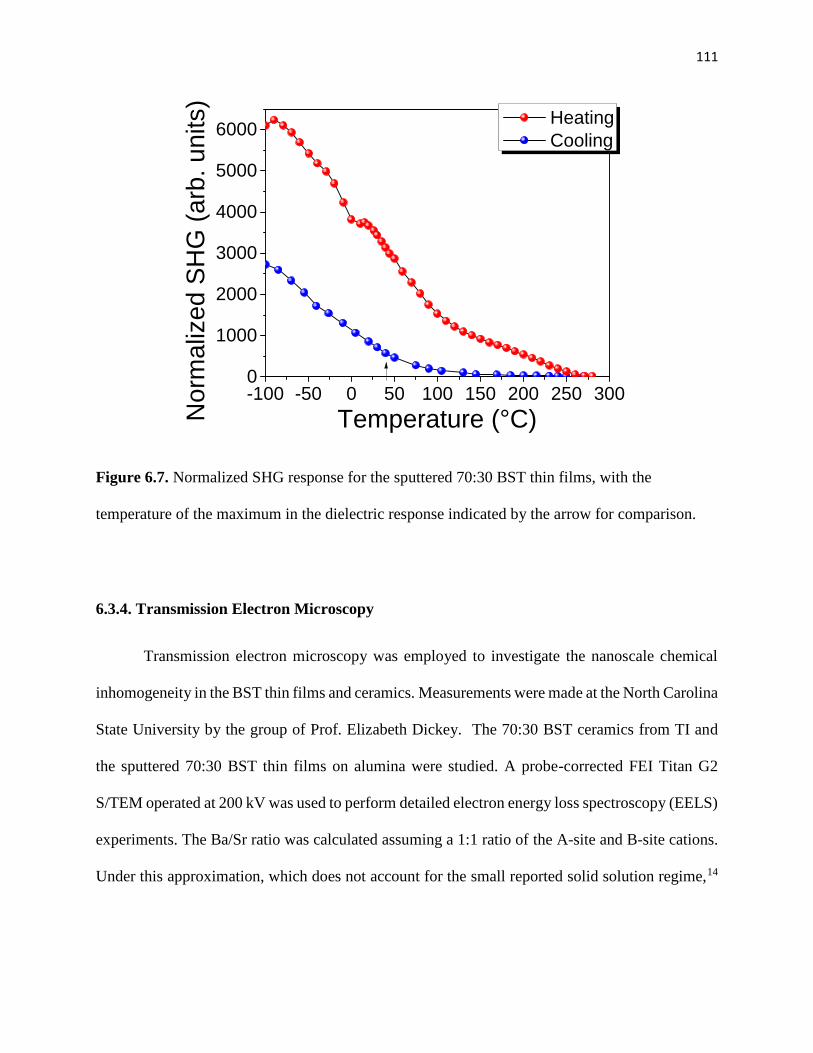
111
-100 -50 0 50 100 150 200 250 3000
1000
2000
3000
4000
5000
6000
Nor
mal
ized
SH
G (a
rb. u
nits
)
Temperature (°C)
Heating Cooling
Figure 6.7. Normalized SHG response for the sputtered 70:30 BST thin films, with the
temperature of the maximum in the dielectric response indicated by the arrow for comparison.
6.3.4. Transmission Electron Microscopy
Transmission electron microscopy was employed to investigate the nanoscale chemical
inhomogeneity in the BST thin films and ceramics. Measurements were made at the North Carolina
State University by the group of Prof. Elizabeth Dickey. The 70:30 BST ceramics from TI and
the sputtered 70:30 BST thin films on alumina were studied. A probe-corrected FEI Titan G2
S/TEM operated at 200 kV was used to perform detailed electron energy loss spectroscopy (EELS)
experiments. The Ba/Sr ratio was calculated assuming a 1:1 ratio of the A-site and B-site cations.
Under this approximation, which does not account for the small reported solid solution regime,14
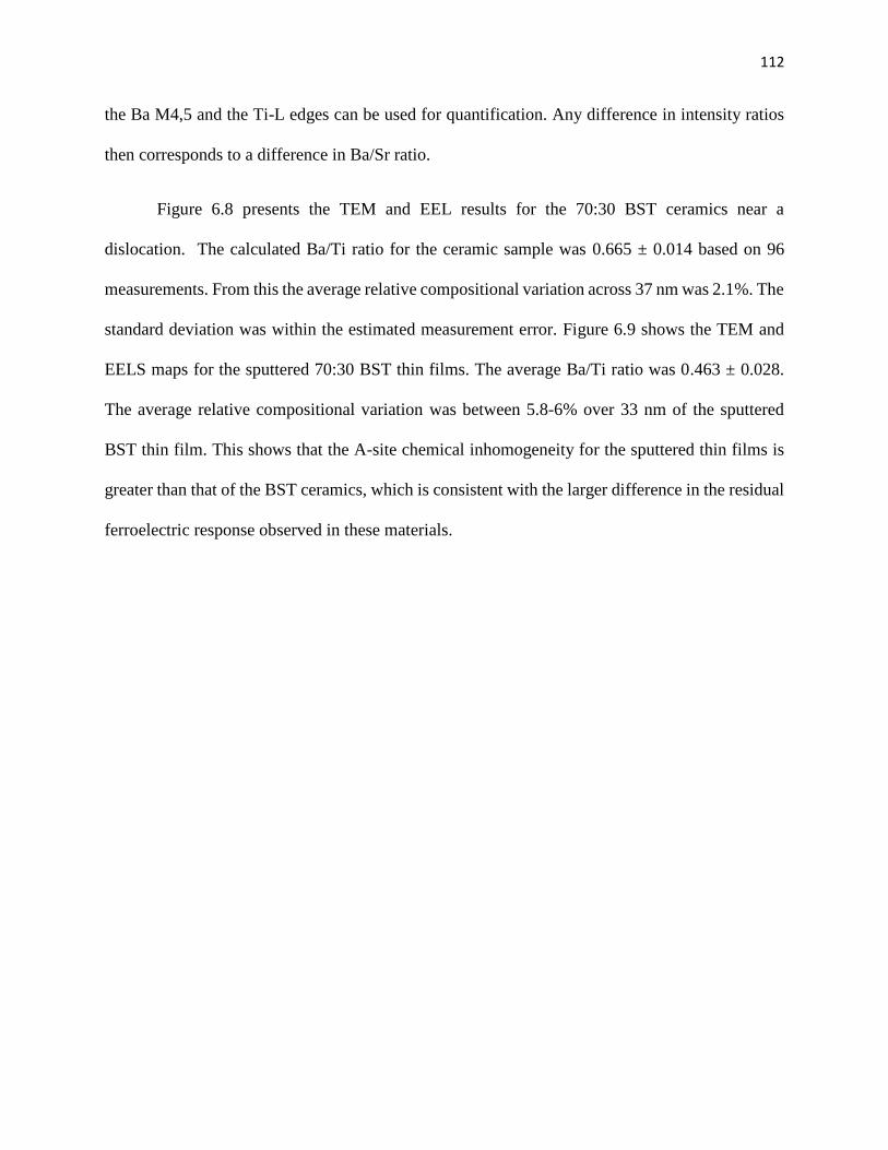
112
the Ba M4,5 and the Ti-L edges can be used for quantification. Any difference in intensity ratios
then corresponds to a difference in Ba/Sr ratio.
Figure 6.8 presents the TEM and EEL results for the 70:30 BST ceramics near a
dislocation. The calculated Ba/Ti ratio for the ceramic sample was 0.665 ± 0.014 based on 96
measurements. From this the average relative compositional variation across 37 nm was 2.1%. The
standard deviation was within the estimated measurement error. Figure 6.9 shows the TEM and
EELS maps for the sputtered 70:30 BST thin films. The average Ba/Ti ratio was 0.463 ± 0.028.
The average relative compositional variation was between 5.8-6% over 33 nm of the sputtered
BST thin film. This shows that the A-site chemical inhomogeneity for the sputtered thin films is
greater than that of the BST ceramics, which is consistent with the larger difference in the residual
ferroelectric response observed in these materials.
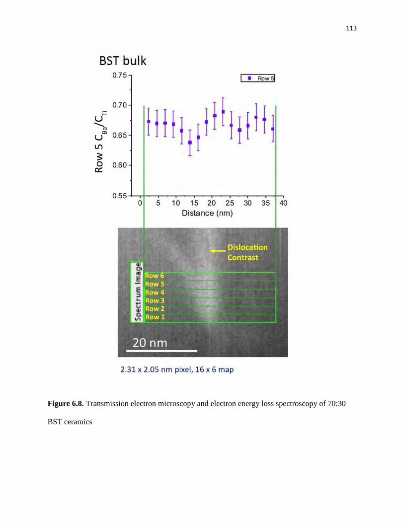
113
Figure 6.8. Transmission electron microscopy and electron energy loss spectroscopy of 70:30
BST ceramics
Row
5 C
Ba/C
Ti
114
Figure 6.9. Transmission electron microscopy and electron energy loss spectroscopy of
sputtered 70:30 BST thin films
Row
5 C
Ba/C
Ti
115
6.4. Conclusion
In this chapter the residual ferroelectric behavior in barium strontium titanate thin films
and ceramics was characterized through electrical, optical and physical methods. The existence of
polar clusters was observed in the dielectric, Rayleigh and SHG response. The development of
polar clusters was also found to be greater in samples with increased chemical inhomogeneity. The
presence of polar clusters above the transition temperature corroborates the residual ferroelectric
response measured in these materials. Variations in chemical inhomogeneity agree with the
temperature extent of the residual ferroelectric response.
6.5. References
1. Tiggelman, M. P. J., Reimann, K., Van Rijs, F., Schmitz, J. & Hueting, R. J. E. On the trade-
off between quality factor and tuning ratio in tunable high-frequency capacitors. IEEE Trans.
Electron Devices 56, 2128–2136 (2009).
2. A. Soukiassian D. A. Tenne. Raman study of BaxSr1-xTiO3 films: Evidence for the existence
of polar nanoregions. Phys. Rev. B, 67, 012302 (2003).
3. Zhou, L., Vilarinho, P. M., Baptista, J. L., Dependence of the structural and dielectric
properties of Ba1- xSrxTiO3 ceramic solid solutions on raw material processing. J. Eur. Ceram.
Soc. 19, 2015–2020 (1999).
4. Garten, L. M., Lam, P., Harris, D., Maria, J.-P. & Trolier-McKinstry, S. Residual
ferroelectricity in barium strontium titanate thin film tunable dielectrics. J. Appl. Phys. 116,
044104 (2014).
116
5. Ma, W. & Cross, L. E. Flexoelectric polarization of barium strontium titanate in the
paraelectric state. Appl. Phys. Lett. 81, 3440–3442 (2002).
6. Samara, G. A. The relaxational properties of compositionally disordered ABO3 perovskites. J.
Phys. Condens. Matter 15, R367 (2003).
7. N. Bassiri Gharb. Dielectric and Piezoelectric Nonlinearities in Oriented Pb(Yb1/2Nb1/2)O3-
PbTiO3 Thin Films. Ph.D. dissertation, Dept. of Mat. Sci and Eng., Penn. State University,
University Park, PA, 2005.
8. Ko, J.-H., Kim, T. H., Roleder, K., Rytz, D. & Kojima, S. Precursor dynamics in the
ferroelectric phase transition of barium titanate single crystals studied by Brillouin light
scattering. Phys. Rev. B 84, 094123 (2011).
13. Scott, J. F., Jiang, A., Redfern, S. A. T., Zhang, M. & Dawber, M. Infrared spectra and
second-harmonic generation in barium strontium titanate and lead zirconate-titanate thin
films: Polaron artifacts. J. Appl. Phys. 94, 3333–3344 (2003).
10. Lee, S., Randall, C. A. & Liu, Z.-K. Modified phase diagram for the barium oxide–titanium
dioxide system for the ferroelectric barium titanate. J. Am. Ceram. Soc. 90, 2589–2594
(2007).
117
Chapter 7
The Flexoelectric Response in BST
7.1. Introduction
Interest in flexoelectricity has intensified after reports of flexoelectric coefficients
exceeding 100 µC/m in barium strontium titanate (BST), which is six orders of magnitude higher
than theoretically predicted.1,2,3 Flexoelectricity describes the development of polarization due to
the application of a strain gradient, or conversely the development of a strain which increases
linearly with an electric field gradient.2,4 Flexoelectric phenomenology predicts a linear
relationship between the polarizability of the material and the polarization which develops due to
an applied strain gradient. The constant of proportionality is known as the flexocoupling
coefficient. Theoretical predictions of the flexocoupling coefficient extend from 1-10 Volts.5,6
Models of flexocoupling in perovskites suggest that anything exceeding 10-15 Volts will
destabilize the perovskite structure, producing an incommensurate phase.2 Despite this,
flexocoupling coefficients of 850 Volts have been reported for BST.1,2 Thus, the anomalously large
and varied flexocoupling coefficients in BST challenge a simple interpretation of the flexoelectric
effect in paraelectric materials. An improved understanding of this heightened response would
facilitate the development of novel flexoelectric-based sensors and energy harvesters.2,7,8
Any local structural distortions, such as nanopolar regions, ferroelectricity, defects, or self-
polarization could influence the measured flexoelectric response. Tagantsev has also suggested
that surface piezoelectricity and flexoelectricity contribute to the overall flexoelectric response.9
Surface flexoelectricity, although unique to the particular surface chemistry, is predicted to be on
118
the order of ~10-10 C/m.4,3 In a study on GaN based quantum dots, a fifty percent reduction in the
modeled internal electric field occurred due to defect modulated flexoelectricity, for a flexoelectric
response in the nC/m.. Additionally, self-polarization induced through localized space charge,
asymmetric Schottky barriers and/or defect dipoles could contribute to flexoelectricity.10,11 Local
strains associated with interfaces, grain boundaries, or defects have also been reported to produce
polarization in the incipient ferroelectric SrTiO3;12,13,14 for example, strain gradients on the order
of 10-7 m-1 reported in the vicinity of defects could produce localized polarizations of 1-10
µC/cm2.15 Defects alone, however, still do not account for the reported flexoelectric constants
observed in BST.15
Another potential source of enhanced flexoelectricity is ferroelectricity. It stands to reason
that the measured flexoelectric polarization would be significantly increased by the large
reorientable spontaneous polarization which develops in ferroelectrics. Recent reports in relaxor
ferroelectric materials show a correlation between the onset of nano-polar regions and increased
flexoelectric repsonse.16,17 Narvaez and Catalan observed hysteresis in the flexoelectric response
upon heating and cooling, associated changes in elasticity, and enhanced flexocoupling which
persist up to the temperature where the nanopolar regions disappeared.16 It is notable that relaxor
behavior has also been observed in Ba1-xSrxTiO3, as described in the previous chapter.
Furthermore, many perovskites which can become ferroelectric also display abnormally
large flexocoupling coefficients. For example, the flexocoupling factors measured in the
paraelectric phase are: BaTiO3 f≈560V, PMN-PT f≈110-270V, Pb0.3Sr0.7TiO3 f≈170V,
Pb(Zr,Ti)O3 f≈72).18,2,3,19 Many of these flexocoupling measurements were acquired within a few
degrees of the paraelectric-ferroelectric phase transition, a region in which ferroelectricity likely
119
persists. In contrast, SrTiO3, which does not become ferroelectric at any temperature, displays
significantly smaller flexoelectric responses and flexocoupling factors. For example, in undoped,
high purity SrTiO3 the predicted transverse flexoelectric coefficients is ~ 2.3 nC/m and the
measured response is 4 nC/m, which is well below the 100 µC/m observed in BST.15,20, All of
these results point to the importance of understanding the interactions between ferroelectricity and
flexoelectricity.
Significant enhancements in flexocoupling have been observed in relaxor ferroelectrics
like PMN-PT, BST, and Ba(Ti0.87,Sn0.13)O3, close to Tmax.1,3,21 The accessibility of a high
permittivity, low temperature ferroelectric to paraelectric phase transition in BST offers an
opportunity to study flexoelectricity near TC in order to provide answers to the disparity between
the theoretical and measured flexoelectric response.
This work addresses several questions concerning the mechanisms of enhanced
flexoelectric coupling in Ba1-xSrxTiO3. In particular, it is proposed that the flexoelectric coupling
is enhanced by the existence of nano/micropolar regions above TC in BST. A direct comparison is
made between the residual ferroelectric contributions in the paraelectric phase, which are
characterized by the irreversible Rayleigh behavior, and the temperature dependences of the
flexoelectric response. Direct measurements of the flexoelectric poling are discussed and then
compared to the strain gradient induced polarization and induced piezoelectric response.
7.2. Methods
The barium strontium titanate ceramics used in this analysis were developed at Texas
Instruments using a wet chemistry route in order to maintain strict control over the A-site
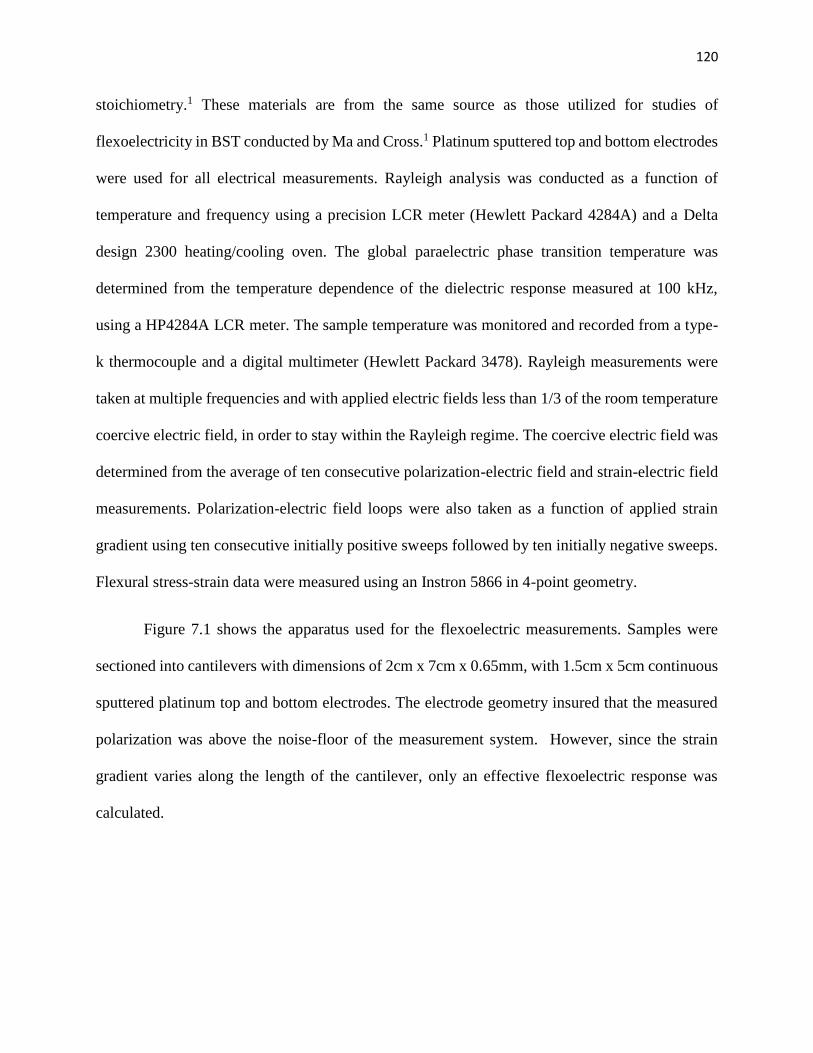
120
stoichiometry.1 These materials are from the same source as those utilized for studies of
flexoelectricity in BST conducted by Ma and Cross.1 Platinum sputtered top and bottom electrodes
were used for all electrical measurements. Rayleigh analysis was conducted as a function of
temperature and frequency using a precision LCR meter (Hewlett Packard 4284A) and a Delta
design 2300 heating/cooling oven. The global paraelectric phase transition temperature was
determined from the temperature dependence of the dielectric response measured at 100 kHz,
using a HP4284A LCR meter. The sample temperature was monitored and recorded from a type-
k thermocouple and a digital multimeter (Hewlett Packard 3478). Rayleigh measurements were
taken at multiple frequencies and with applied electric fields less than 1/3 of the room temperature
coercive electric field, in order to stay within the Rayleigh regime. The coercive electric field was
determined from the average of ten consecutive polarization-electric field and strain-electric field
measurements. Polarization-electric field loops were also taken as a function of applied strain
gradient using ten consecutive initially positive sweeps followed by ten initially negative sweeps.
Flexural stress-strain data were measured using an Instron 5866 in 4-point geometry.
Figure 7.1 shows the apparatus used for the flexoelectric measurements. Samples were
sectioned into cantilevers with dimensions of 2cm x 7cm x 0.65mm, with 1.5cm x 5cm continuous
sputtered platinum top and bottom electrodes. The electrode geometry insured that the measured
polarization was above the noise-floor of the measurement system. However, since the strain
gradient varies along the length of the cantilever, only an effective flexoelectric response was
calculated.
121
Figure 7.1. Schematic of the flexoelectric testing system and flexoelectric response
For the measurement system, lock-in amplifiers (Stanford Research SR830 DSP) were
employed to simultaneously measure the charge output of the two orthogonal components of
dynamic strain, while the static strain was measured by an amplified Wheatstone bridge. The
strain gradient was measured via commercial strain gauges (Omega) attached to the top and bottom
surfaces of the sample, parallel to the long axis of the cantilever as shown in Figure 1. The strain
gradient was calculated from the output of the top and bottom gauge and the thickness of the
sample as shown:
∇ = ( − )where t is the thickness and st, the strain at the upper surface, and sb is the strain at the lower
surface. The d33 piezoelectric measurements were taken on a Berlincourt meter (ZJ-2, Institute of
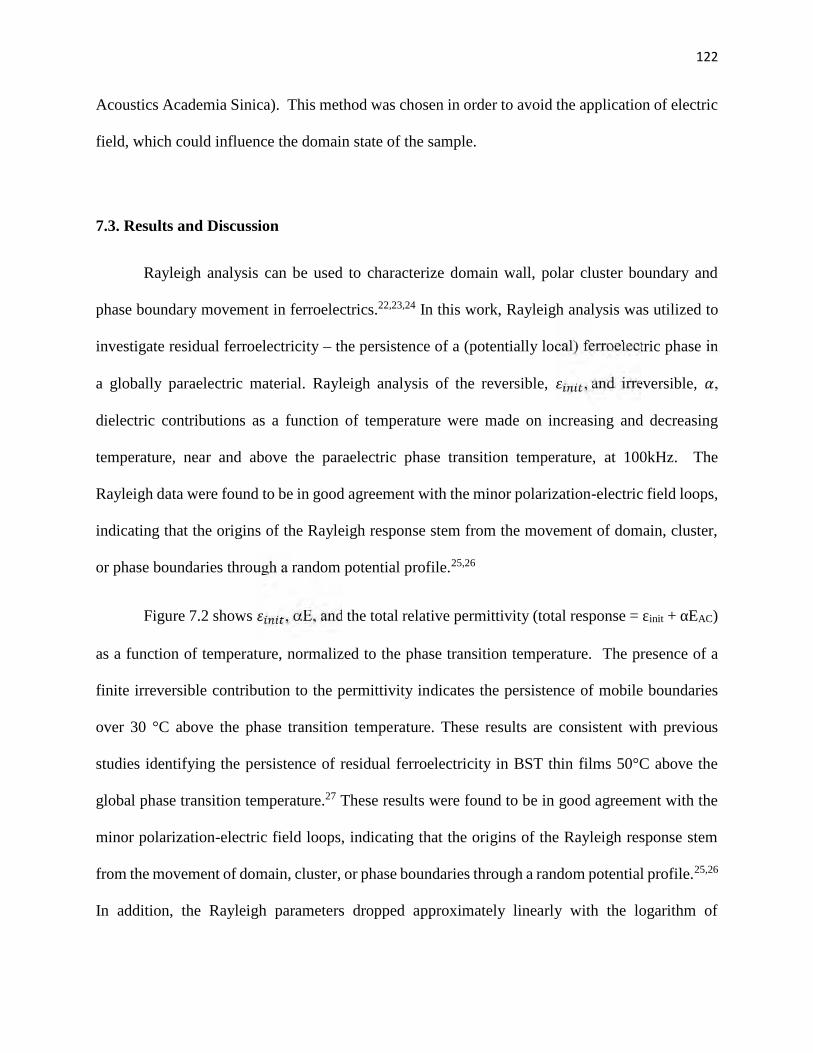
122
Acoustics Academia Sinica). This method was chosen in order to avoid the application of electric
field, which could influence the domain state of the sample.
7.3. Results and Discussion
Rayleigh analysis can be used to characterize domain wall, polar cluster boundary and
phase boundary movement in ferroelectrics.22,23,24 In this work, Rayleigh analysis was utilized to
investigate residual ferroelectricity – the persistence of a (potentially local) ferroelectric phase in
a globally paraelectric material. Rayleigh analysis of the reversible, , and irreversible, ,
dielectric contributions as a function of temperature were made on increasing and decreasing
temperature, near and above the paraelectric phase transition temperature, at 100kHz. The
Rayleigh data were found to be in good agreement with the minor polarization-electric field loops,
indicating that the origins of the Rayleigh response stem from the movement of domain, cluster,
or phase boundaries through a random potential profile.25,26
Figure 7.2 shows , E, and the total relative permittivity (total response = εinit + αEAC)
as a function of temperature, normalized to the phase transition temperature. The presence of a
finite irreversible contribution to the permittivity indicates the persistence of mobile boundaries
over 30 °C above the phase transition temperature. These results are consistent with previous
studies identifying the persistence of residual ferroelectricity in BST thin films 50°C above the
global phase transition temperature.27 These results were found to be in good agreement with the
minor polarization-electric field loops, indicating that the origins of the Rayleigh response stem
from the movement of domain, cluster, or phase boundaries through a random potential profile.25,26
In addition, the Rayleigh parameters dropped approximately linearly with the logarithm of
123
frequency, as has previously been reported for ferroelectric domain walls.25,28 The residual
ferroelectricity also adds a contribution to dielectric loss under applied electric fields. For the AC
electric fields used during Rayleigh analysis, less than 0.3 kV/cm, the dielectric loss increased by
38% at Tmax relative to the small signal value.
0 10 20 30 40 50 60 70 80
20
40
60
80
100
Flex
oele
ctric
coe
ffcie
nt
(C
/m)
T-Tc (°C)
(Ma and Cross)*EAC
init
Total Rayleigh
0
5000
10000
15000
20000
Tota
l Ray
leig
h re
spon
se,
init,
E AC
Figure 7.2. Temperature dependence of the Rayleigh response and flexoelectric coefficient (Ma
and Cross), normalized to the ferroelectric-paraelectric phase transition temperature
It is important to note that the temperature extent of the observed residual ferroelectricity
overlaps with the temperature range over which anomalously high flexoelectric coupling constants
are reported.2,4 This both provide an extrinsic contribution to the polarization, and may also
produce local strain gradients which add to the flexoelectric response.2
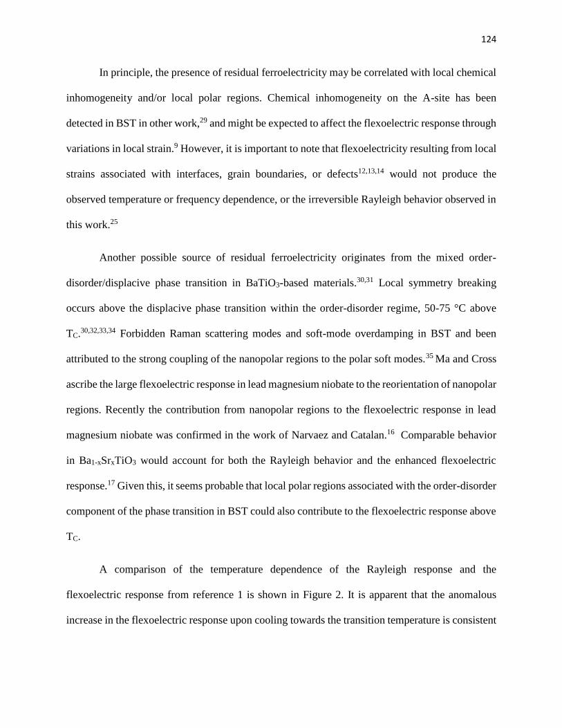
124
In principle, the presence of residual ferroelectricity may be correlated with local chemical
inhomogeneity and/or local polar regions. Chemical inhomogeneity on the A-site has been
detected in BST in other work,29 and might be expected to affect the flexoelectric response through
variations in local strain.9 However, it is important to note that flexoelectricity resulting from local
strains associated with interfaces, grain boundaries, or defects12,13,14 would not produce the
observed temperature or frequency dependence, or the irreversible Rayleigh behavior observed in
this work.25
Another possible source of residual ferroelectricity originates from the mixed order-
disorder/displacive phase transition in BaTiO3-based materials.30,31 Local symmetry breaking
occurs above the displacive phase transition within the order-disorder regime, 50-75 °C above
TC.30,32,33,34 Forbidden Raman scattering modes and soft-mode overdamping in BST and been
attributed to the strong coupling of the nanopolar regions to the polar soft modes.35 Ma and Cross
ascribe the large flexoelectric response in lead magnesium niobate to the reorientation of nanopolar
regions. Recently the contribution from nanopolar regions to the flexoelectric response in lead
magnesium niobate was confirmed in the work of Narvaez and Catalan.16 Comparable behavior
in Ba1-xSrxTiO3 would account for both the Rayleigh behavior and the enhanced flexoelectric
response.17 Given this, it seems probable that local polar regions associated with the order-disorder
component of the phase transition in BST could also contribute to the flexoelectric response above
TC.
A comparison of the temperature dependence of the Rayleigh response and the
flexoelectric response from reference 1 is shown in Figure 2. It is apparent that the anomalous
increase in the flexoelectric response upon cooling towards the transition temperature is consistent
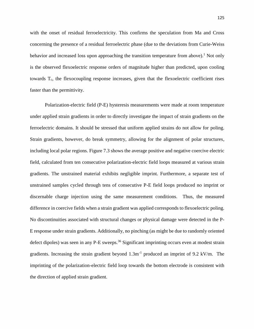
125
with the onset of residual ferroelectricity. This confirms the speculation from Ma and Cross
concerning the presence of a residual ferroelectric phase (due to the deviations from Curie-Weiss
behavior and increased loss upon approaching the transition temperature from above).1 Not only
is the observed flexoelectric response orders of magnitude higher than predicted, upon cooling
towards Tc, the flexocoupling response increases, given that the flexoelectric coefficient rises
faster than the permittivity.
Polarization-electric field (P-E) hysteresis measurements were made at room temperature
under applied strain gradients in order to directly investigate the impact of strain gradients on the
ferroelectric domains. It should be stressed that uniform applied strains do not allow for poling.
Strain gradients, however, do break symmetry, allowing for the alignment of polar structures,
including local polar regions. Figure 7.3 shows the average positive and negative coercive electric
field, calculated from ten consecutive polarization-electric field loops measured at various strain
gradients. The unstrained material exhibits negligible imprint. Furthermore, a separate test of
unstrained samples cycled through tens of consecutive P-E field loops produced no imprint or
discernable charge injection using the same measurement conditions. Thus, the measured
difference in coercive fields when a strain gradient was applied corresponds to flexoelectric poling.
No discontinuities associated with structural changes or physical damage were detected in the P-
E response under strain gradients. Additionally, no pinching (as might be due to randomly oriented
defect dipoles) was seen in any P-E sweeps.36 Significant imprinting occurs even at modest strain
gradients. Increasing the strain gradient beyond 1.3m-1 produced an imprint of 9.2 kV/m. The
imprinting of the polarization-electric field loop towards the bottom electrode is consistent with
the direction of applied strain gradient.
126
0.0 0.2 0.4 0.6 0.8 1.0 1.2 1.440000
44000
48000
52000
Elec
tric
Fiel
d (V
/m)
Strain Gradient (m-1)
+Ec
l-Ecl
Figure 7.3. Impact of applied strain gradient on the coercive field of a flexoelectric sample
showing flexo-poling and residual imprint upon removal of the electric field.
Upon the removal of the strain gradient, a residual imprint of approximately 9.0 kV/m is
maintained. This persistent bias did not decay over a period of hours. It is hypothesized that this
might be due to the strain-gradient-induced alignment of defect dipoles that could not be reoriented
using electric field cycling alone. These results suggest that flexo-poling would be a viable option
for materials too leaky to withstanding electric poling. Furthermore, they also confirm that
flexoelectric measurements in a material with some ferroelectric contribution (presumably either
long or short range ordered) will be enhanced by the response of the pre-existing polarization.
The observations of reorientation of polar structures under applied strain gradient is consistent
with previous observations.37,38
127
Changes in the piezoelectric response in lead zirconate titanate and BaTiO3 thin films
measured via piezoresponse force microscopy have also been attributed to flexoelectric poling.39,40
Flexoelectric poling was also observed in ferroelectric lead zirconate titanate ceramics, as shown
in Figure 7.4 as a change in slope.19
Figure 7.4. The polarization as a function of applied strain gradient in lead zirconate titanate19
This work established that the largest flexoelectric response in BST samples are measured
while the material has local polar regions, and that the application of a strain gradient influences
the alignment of the ferroelectric domain structure.
In order to directly study the impact of ferroelectricity on the flexoelectric response, a
measurement apparatus was developed to characterize the flexoelectric polarization as a function
of applied static and dynamic strain gradients. Remanent piezoelectric d33 measurements were
made prior to and after each flexoelectric measurement using a Berlincourt meter, to assess the
alignment of the polarization due to the applied strain gradient.
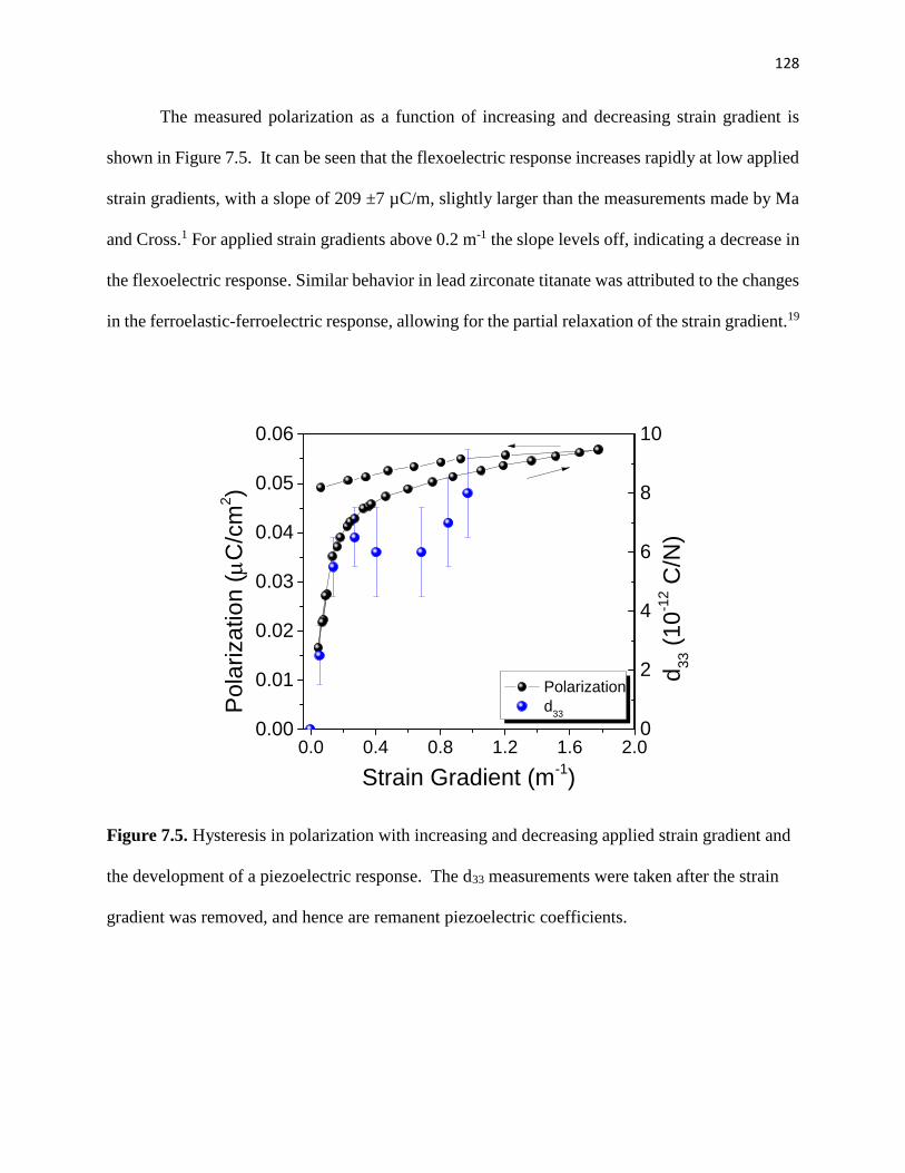
128
The measured polarization as a function of increasing and decreasing strain gradient is
shown in Figure 7.5. It can be seen that the flexoelectric response increases rapidly at low applied
strain gradients, with a slope of 209 ±7 µC/m, slightly larger than the measurements made by Ma
and Cross.1 For applied strain gradients above 0.2 m-1 the slope levels off, indicating a decrease in
the flexoelectric response. Similar behavior in lead zirconate titanate was attributed to the changes
in the ferroelastic-ferroelectric response, allowing for the partial relaxation of the strain gradient.19
0.0 0.4 0.8 1.2 1.6 2.00.00
0.01
0.02
0.03
0.04
0.05
0.06
Polarization d33Po
lariz
atio
n (
C/c
m2 )
Strain Gradient (m-1)
0
2
4
6
8
10
d 33 (1
0-12 C
/N)
Figure 7.5. Hysteresis in polarization with increasing and decreasing applied strain gradient and
the development of a piezoelectric response. The d33 measurements were taken after the strain
gradient was removed, and hence are remanent piezoelectric coefficients.
129
The data in Fig. 7.6 on the remanent piezoelectric measurements show no initial d33, which
is consistent with an unpoled ferroelectric. However, after removal of the applied strain gradient
there is a persistent polarization which produces the remanent d33. These results are consistent with
the flexo-poling results discussed previously. Although the piezoelectric response is small, the
presence of piezoelectricity shows definitively that the flexoelectric measurement led to permanent
changes in the alignment of the polar structures, and thus a non-flexoelectric enhancement to the
polarization.
The Rayleigh analysis, flexoelectric poling and synchronized flexoelectric-piezoelectric
measurements support the role of residual ferroelectricity in enhancing flexoelectricity in ceramic
Ba1-xSrxTiO3. Local polar regions, associated with the order-disorder phenomena, would account
for the observed residual ferroelectric behavior above TC and the enhanced flexo-poling induced
polarization, akin to what has been observed in relaxor ferroelectrics.25 Although this is the first
reported use of Rayleigh analysis above Tc in bulk BST ceramics, it can be inferred that residual
ferroelectricity is likely prevalent, as evidenced by the hysteresis in the field dependence of
permittivity, piezoelectricity in the paraelectric phase, or excessive dielectric loss observed in
many studies.42,43,44,45 In the ferroelectric phase, piezoelectricity in BST provides some
contribution to the total measured polarization under strain/strain gradient.
Given the fact that the motion of mobile interfaces contributes to the measured flexoelectric
response above TC, the processing, thermal, and elastic history should be expected to influence the
measured flexoelectric response. This explains the anomalously large and diverse flexocoupling
coefficients which have been reported.2 As inconsistencies in flexocoupling are common amongst
130
ferroelectric perovskites, it is likely that ferroelectricity plays a role in the discrepancies observed
in these materials as well.
7.4. Conclusions
In summary, residual ferroelectricity was observed in Ba1-xSrxTiO3 ceramics 30°C above
the global phase transition temperature, within the temperature range commonly employed for
flexoelectric measurements. Furthermore, the application of a strain gradient lead to strain
gradient-induced poling, or flexoelectric poling, as observed by the development of remanent
polarization in flexoelectric measurements, an induced d33 piezoelectric response and the
production of an internal permanent bias within the polarization-electric field loops. All of these
results point towards the flexoelectric poling of the residual ferroelectric response as the source of
the observed enhancements in flexoelectric response.
7.5. References
1. Ma, W. & Cross, L. E. Flexoelectric polarization of barium strontium titanate in the
paraelectric state. Appl. Phys. Lett. 81, 3440–3442 (2002).
2. Zubko, P., Catalan, G. & Tagantsev, A. K. Flexoelectric Effect in Solids. Annu. Rev. Mater.
Res. 43, 387–421 (2013).
3. Cross, L. E. Flexoelectric effects: Charge separation in insulating solids subjected to elastic
strain gradients. J. Mater. Sci. 41, 53–63 (2006).
131
4. Fu, J. Y., Zhu, W., Li, N. & Cross, L. E. Experimental studies of the converse flexoelectric
effect induced by inhomogeneous electric field in a barium strontium titanate composition. J.
Appl. Phys. 100, 024112 (2006).
5. Kogan, Sh M. Piezoelectric effect during inhomogeneous deformation and acoustic scattering
of carriers in crystals. Sov. Phys.-Solid State 5 2069–2070 (1964).
6. Tagantsev, A. K. Piezoelectricity and flexoelectricity in crystalline dielectrics. Phys. Rev. B
34, 5883–5889 (1986).
7. Kwon, S. R., Huang, W. B., Zhang, S. J., Yuan, F. G. & Jiang, X. N. Flexoelectric sensing
using a multilayered barium strontium titanate structure. Smart Mater. Struct. 22, 115017
(2013).
8. Huang, W., Kwon, S.-R., Zhang, S., Yuan, F.-G. & Jiang, X. A trapezoidal flexoelectric
accelerometer. J. Intell. Mater. Syst. Struct. 25, 271-277 (2013).
9. Tagantsev, A. K. Pyroelectric, piezoelectric, flexoelectric, and thermal polarization effects in
ionic crystals. Sov. Phys. Uspekhi 30, 588 (1987).
10. Afanas’ev, V. P., Pronin, I. P. & Kholkin, A. L. Formation and relaxation mechanisms of
the self-polarization in thin ferroelectric films. Phys. Solid State 48, 1214–1218 (2006).
11. Jiangpeng Chen, Y. L. Upward ferroelectric self-polarization induced by compressive
epitaxial strain in (001) BaTiO3 films. J. Appl. Phys. 113, 20 (2013).
12. Pertsev, N. A., Tagantsev, A. K. & Setter, N. Phase transitions and strain-induced
ferroelectricity in SrTiO3 epitaxial thin films. Phys. Rev. B 61, R825–R829 (2000).
13. Uwe, H., Yamaguchi, H. & Sakudo, T. Ferroelectric microregion in KTa1−xNbxO3 and
SrTiO3. Ferroelectrics 96, 123–126 (1989).
132
14. Petzelt, J., Ostapchuk, T., Pashkin, A. & Rychetský, I. FIR and near-millimetre dielectric
response of SrTiO3, BaTiO3 and BST films and ceramics. J. Eur. Ceram. Soc. 23, 2627–2632
(2003).
15. Zubko, P., Catalan, G., Buckley, A., Welche, P. R. L. & Scott, J. F. Strain-Gradient-
Induced polarization in SrTiO3 single crystals. Phys. Rev. Lett. 99, 167601 (2007).
16. Narvaez, J. & Catalan, G. Origin of the enhanced flexoelectricity of relaxor ferroelectrics.
Appl. Phys. Lett. 104, 162903 (2014).
17. Ma, W. & Cross, L. E. Large flexoelectric polarization in ceramic lead magnesium
niobate. Appl. Phys. Lett. 79, 4420–4422 (2001).
18. Ma, W. & Cross, L. E. Flexoelectricity of barium titanate. Appl. Phys. Lett. 88, 232902
(2006).
19. Ma, W. & Cross, L. E. Strain-gradient-induced electric polarization in lead zirconate
titanate ceramics. Appl. Phys. Lett. 82, 3293–3295 (2003).
20. Xu, T., Wang, J., Shimada, T. & Kitamura, T. Direct approach for flexoelectricity from
first-principles calculations: cases for SrTiO3 and BaTiO3. J. Phys. Condens. Matter 25,
415901 (2013).
21.Shu, L., Wei, X., Jin, L., Li, Y., Wang, H., & Yao, X. Enhanced direct flexoelectricity in
paraelectric phase of Ba(Ti0.87Sn0.13)O3 ceramics. Appl. Phys. Lett. 102, 152904 (2013).
22. Rayleigh, Lord. XXV. Notes on electricity and magnetism.—III. On the behaviour of
iron and steel under the operation of feeble magnetic forces. Philos. Mag. Ser. 5 23, 225–245
(1887).
23. Damjanovic, D., Taylor, D. Contributions to the nonlinear dielectric and piezoelectric
response of ferroelectric thin films and ceramics. Ferroelectrics, 221.1, 137-146. (1999).
133
24. Jin, L., Porokhonskyy, V. & Damjanovic, D. Domain wall contributions in Pb(Zr,Ti)O3
ceramics at morphotropic phase boundary: A study of dielectric dispersion. Appl. Phys. Lett.
96, 242902 (2010).
25. Taylor, D. V. & Damjanovic, D. Evidence of domain wall contribution to the dielectric
permittivity in PZT thin films at sub-switching fields. J. Appl. Phys. 82, 1973–1975 (1997).
26. N. Bassiri Gharb. Dielectric and Piezoelectric Nonlinearities in Oriented Pb(Yb1/2Nb1/2)O3-
PbTiO3 Thin Films. Ph.D. dissertation, Dept. of Mat. Sci and Eng., Penn. State University,
University Park, PA, 2005.
27. Garten, L. M., Lam, P., Harris, D., Maria, J.-P. & Trolier-McKinstry, S. Residual
ferroelectricity in barium strontium titanate thin film tunable dielectrics. J. Appl. Phys. 116,
044104 (2014).
28. Bassiri-Gharb, N., Fujii, I., Hong, E.,Trolier-McKinstry, S., Taylor, D. V., Damjanovic, D.,
Domain wall contributions to the properties of piezoelectric thin films. J. Electroceramics 19,
49–67 (2007).
29. Tikhomirov, O., Jiang, H. & Levy, J. Direct observation of local ferroelectric phase
transitions in BaxSr1−xTiO3 thin films. Appl. Phys. Lett. 77, 2048–2050 (2000).
30. Bussmann-Holder, A., Beige, H. & Völkel, G. Precursor effects, broken local symmetry, and
coexistence of order-disorder and displacive dynamics in perovskite ferroelectrics. Phys. Rev.
B 79, 184111 (2009).
31. D. A. Tenne, A. Soukiassian, X. X. Xi, H. Choosuwan, R. Guo, and A. S. Bhalla, “Lattice
dynamics in BaxSr1−xTiO3 thin films studied by Raman spectroscopy,” Journal of Applied
Physics, vol. 96, no. 11, pp. 6597–6605, Nov. 2004.
134
32. Ko, J.-H., Kim, T. H., Roleder, K., Rytz, D. & Kojima, S. Precursor dynamics in the
ferroelectric phase transition of barium titanate single crystals studied by Brillouin light
scattering. Phys. Rev. B 84, 094123 (2011).
33. Petkov, V., Gateshki, M., Niederberger, M. & Ren, Y. Atomic-Scale Structure of
Nanocrystalline BaxSr1-xTiO3 (x = 1, 0.5, 0) by X-ray Diffraction and the Atomic Pair
Distribution Function Technique. Chem. Mater. 18, 814–821 (2006).
34. Dobal, P. S., Dixit, A., Katiyar, R. S., Garcia, D., Guo, R., & Bhalla, A. S. Micro-Raman
study of Ba1 − xSrxTiO3 ceramics. J. Raman Spectrosc. 32, 147–149 (2001).
35. A. Soukiassian D. A. Tenne. Raman study of BaxSr1-xTiO3 films: Evidence for the existence
of polar nanoregions. Phys. Rev. B 67, 012302 (2003).
36. Robert, G., Damjanovic, D. & Setter, N. Preisach modeling of ferroelectric pinched loops.
Appl. Phys. Lett. 77, 4413–4415 (2000).
37. Catalan, Gustau, A. Lubk, A. H. G. Vlooswijk, E. Snoeck, C. Magen, A. Janssens, G.
Rispens, G. Rijnders, D. H. A. Blank, and B. Noheda. Flexoelectric rotation of polarization in
ferroelectric thin films. Nat. Mater. 10, 963–967 (2011).
38. Lee, D., Yoon, A., Jang S. Y., Yoon, J.-G., Chung, J.-S., Kim, M., Scott, J. F., Noh, T. W.
Giant flexoelectric effect in ferroelectric epitaxial thin films. Phys. Rev. Lett. 107, 057602
(2011).
39. Gruverman, A., Rodriguez, B. J., Kingon, A. I., Nemanich, R. J., Tagantsev, A. K., Cross, J.
S., & Tsukada, M. Mechanical stress effect on imprint behavior of integrated ferroelectric
capacitors. Appl. Phys. Lett. 83, 728–730 (2003).
40. Lu, H., Bark, C. W., De los Ojos, D. E., Alcala, J., Eom, C. B., Catalan, G., & Gruverman, A.
Mechanical Writing of Ferroelectric Polarization. Science 336, 59–61 (2012).
135
41. Gevorgian, S. S. & Kollberg, E. L. Do we really need ferroelectrics in paraelectric phase only
in electrically controlled microwave devices? IEEE Trans. Microw. Theory Tech. 49, 2117–
2124 (2001).
42. Vendik, O. G., Hollmann, E. K., Kozyrev, A. B. & Prudan, A. M. Ferroelectric tuning of
planar and bulk microwave devices. J. Supercond. 12, 325–338 (1999).
43. Nath, R., Zhong, S., Alpay, S. P., Huey, B. D. & Cole, M. W. Enhanced piezoelectric
response from barium strontium titanate multilayer films. Appl. Phys. Lett. 92, 012916 (2008).
44. Fu, C., Yang, C., Chen, H., Hu, L., & Dai, L. Domain configuration and dielectric properties
of Ba0.6Sr0.4TiO3 thin films. Appl. Surf. Sci. 252, 461–465 (2005).
136
Chapter 8
Reliability, Degradation and Failure Mechanisms in Lead Zirconate Titanate Films
8.1 Introduction
As electronics usage grows, defining the limits of reliability and lifetime for electronic
components becomes a priority. The reliability of thin film tunable dielectrics and piezoelectrics
impacts a wide range of applications including personal electronics, sensors, and energy
harvesters.1,2 As with any electrical system, electrical failure can occur under electric field, stress,
or thermal cycling.
Although reliability in bulk BaTiO3 capacitors is understood to be controlled by the
migration of oxygen vacancies under electric fields,3 in PZT thin films there is no consensus on
the dominant conduction mechanisms or lifetime-controlling defect.4 Table 8.1 provides a survey
of the literature on reliability for lead zirconate titanate, PZT, thin films. The first column indicates
the reference, the second the reported conduction mechanism (SC: space charge, PF: Poole-
Frenkel), the next few columns describe the electrodes, the film thickness (t), the deposition
method (CSD: chemical solution deposition, RF: radio frequency sputtering), crystallization
conditions, the method of characterization, the criteria for failure, p or n-type conductivity, and the
activation energy or voltage acceleration factors if reported. The disparate conclusions from each
of these studies highlight the importance of avoiding assumptions about the conduction
mechanisms while developing lifetime models.
137
In this work, the reliability of sputtered and CSD PZT thin films is characterized using highly
accelerated lifetime testing and leakage current-voltage measurements. Lifetime models are
developed based on the dominant conduction mechanisms determined from the measured leakage
current-voltage response. Additionally, supplemental methods of reliability characterization, such
as voltage contrast microscopy are discussed. This chapter also summarizes work from former
group members Manabu Hagiwara and Song Won Ko.
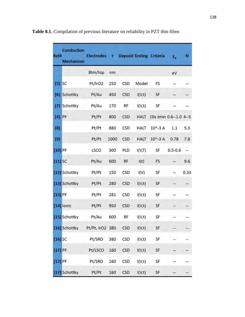
138
Table 8.1. Compilation of previous literature on reliability in PZT thin films567891011121314151617
139
8.2 Methods
Samples were measured from three different PZT thin film sources. Chemical solution
deposited and sputtered, approximately 1 µm thick {100} oriented Pb(Zr0.52,Ti0.48)TiO3 thin films
provided by Samsung Electromechanics. These will be referred to as Sol-gel (100) and Sputtered
(100). Chemical solution deposited Pb(Zr0.52,Ti0.48)TiO3 thin films were also developed at Penn
State. These films were also approximately 1 µm thick and are referred to as PSU sol-gel (111).
All films used top and bottom platinum electrodes.
Leakage current measurements were taken on a 4140 pico-Ampere Meter/DC Voltage
Source (Hewlett Packard). Prior to any current-voltage measurements, the time dependent current
under constant voltage was measured in order to determine the steady state conditions.
Highly accelerated lifetime testing, HALT, was conducted on sputtered and chemical
solution deposited Pb(Zr0.52,Ti0.48)TiO3 thin films provided by Samsung Electromechanics, as well
as films of the same composition made by chemical solution deposition at PSU. 200µm diameter
top platinum electrodes were deposited by sputtering and annealed at 550 °C for two minutes in
flowing oxygen. The films were then sectioned into approximately 1cm by 1cm squares which
were mounted with silver paste to 24 pin DIP packages (Spectrum Semiconductor Materials, Inc.).
After allowing the past to set for 24 hours, the top electrodes were wirebonded (Kulicke and Soffa)
to the contact pads of the package with gold wire as shown in Figure 8.1. Capacitance and dielectric
loss measurements were taken before and after wirebonding to insure no degradation occurred due
to wirebonding. Five samples with approximately 20 capacitors per condition were made for
highly accelerated lifetime testing, for three tests at constant voltage and three at constant
temperature.
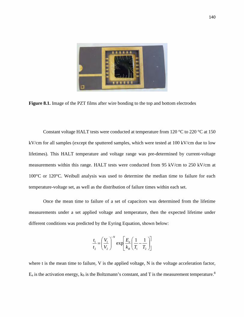
140
Figure 8.1. Image of the PZT films after wire bonding to the top and bottom electrodes
Constant voltage HALT tests were conducted at temperature from 120 °C to 220 °C at 150
kV/cm for all samples (except the sputtered samples, which were tested at 100 kV/cm due to low
lifetimes). This HALT temperature and voltage range was pre-determined by current-voltage
measurements within this range. HALT tests were conducted from 95 kV/cm to 250 kV/cm at
100°C or 120°C. Weibull analysis was used to determine the median time to failure for each
temperature-voltage set, as well as the distribution of failure times within each set.
Once the mean time to failure of a set of capacitors was determined from the lifetime
measurements under a set applied voltage and temperature, then the expected lifetime under
different conditions was predicted by the Eyring Equation, shown below:
212
1
2
1 11exp
TTk
E
V
V
t
t
B
a
N
where t is the mean time to failure, V is the applied voltage, N is the voltage acceleration factor,
Ea is the activation energy, kb is the Boltzmann’s constant, and T is the measurement temperature.8
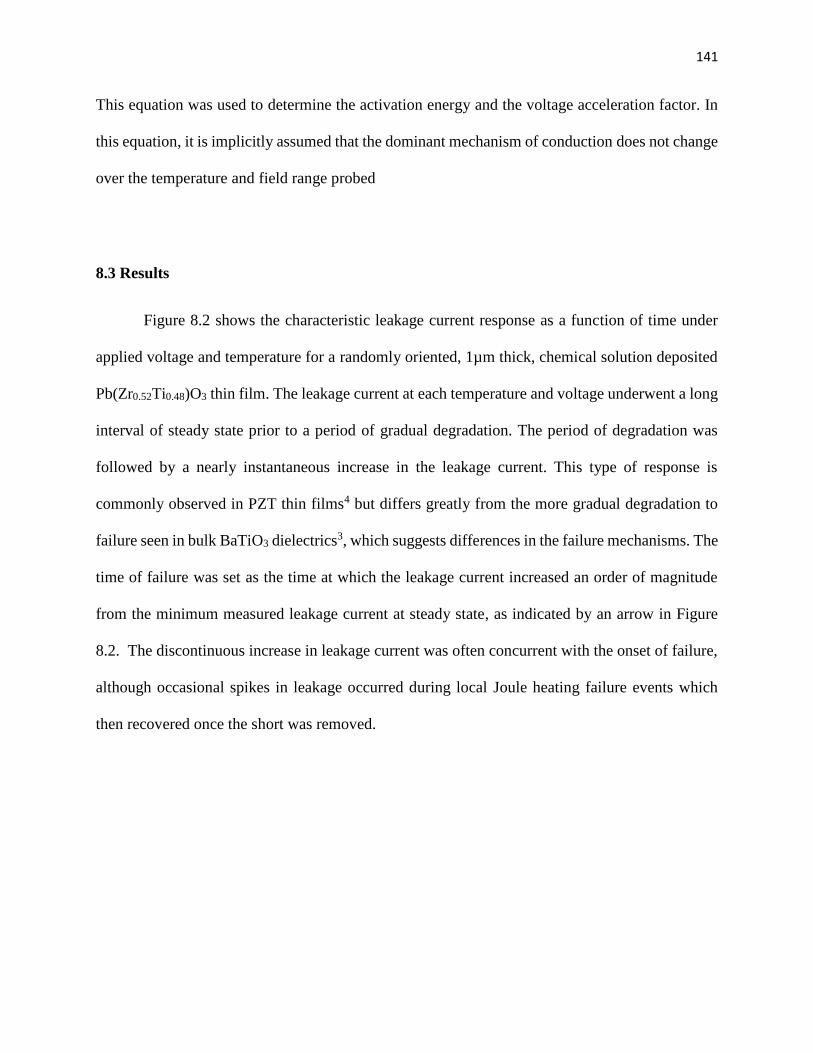
141
This equation was used to determine the activation energy and the voltage acceleration factor. In
this equation, it is implicitly assumed that the dominant mechanism of conduction does not change
over the temperature and field range probed
8.3 Results
Figure 8.2 shows the characteristic leakage current response as a function of time under
applied voltage and temperature for a randomly oriented, 1µm thick, chemical solution deposited
Pb(Zr0.52Ti0.48)O3 thin film. The leakage current at each temperature and voltage underwent a long
interval of steady state prior to a period of gradual degradation. The period of degradation was
followed by a nearly instantaneous increase in the leakage current. This type of response is
commonly observed in PZT thin films4 but differs greatly from the more gradual degradation to
failure seen in bulk BaTiO3 dielectrics3, which suggests differences in the failure mechanisms. The
time of failure was set as the time at which the leakage current increased an order of magnitude
from the minimum measured leakage current at steady state, as indicated by an arrow in Figure
8.2. The discontinuous increase in leakage current was often concurrent with the onset of failure,
although occasional spikes in leakage occurred during local Joule heating failure events which
then recovered once the short was removed.
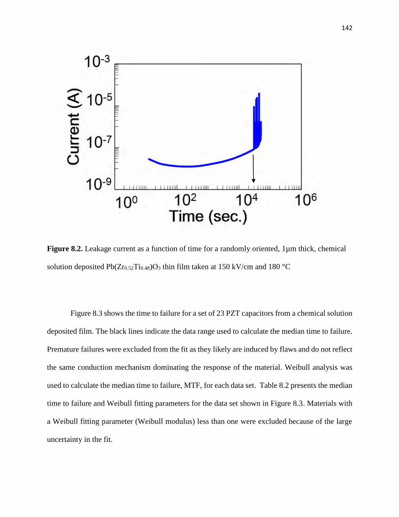
142
Figure 8.2. Leakage current as a function of time for a randomly oriented, 1µm thick, chemical
solution deposited Pb(Zr0.52Ti0.48)O3 thin film taken at 150 kV/cm and 180 °C
Figure 8.3 shows the time to failure for a set of 23 PZT capacitors from a chemical solution
deposited film. The black lines indicate the data range used to calculate the median time to failure.
Premature failures were excluded from the fit as they likely are induced by flaws and do not reflect
the same conduction mechanism dominating the response of the material. Weibull analysis was
used to calculate the median time to failure, MTF, for each data set. Table 8.2 presents the median
time to failure and Weibull fitting parameters for the data set shown in Figure 8.3. Materials with
a Weibull fitting parameter (Weibull modulus) less than one were excluded because of the large
uncertainty in the fit.
143
Figure 8.3. The time to failure for data sets at three temperatures from a CSD PZT thin film
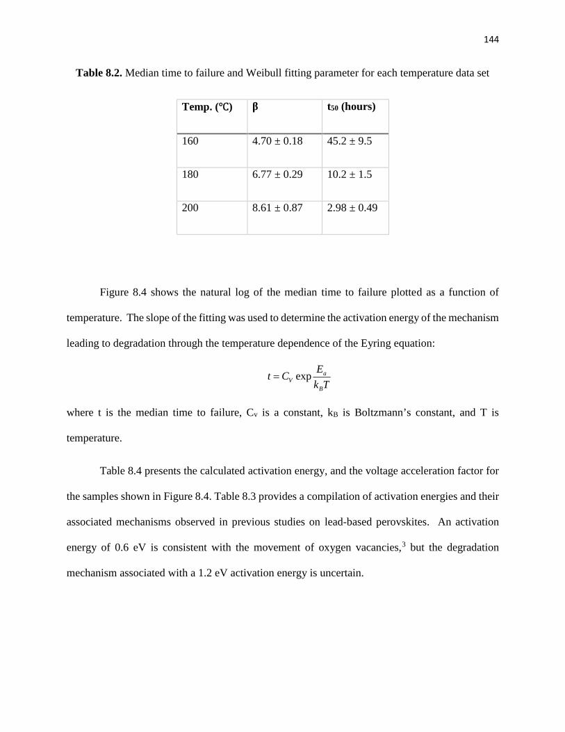
144
Table 8.2. Median time to failure and Weibull fitting parameter for each temperature data set
Temp. (℃) β t50 (hours)
160 4.70 ± 0.18 45.2 ± 9.5
180 6.77 ± 0.29 10.2 ± 1.5
200 8.61 ± 0.87 2.98 ± 0.49
Figure 8.4 shows the natural log of the median time to failure plotted as a function of
temperature. The slope of the fitting was used to determine the activation energy of the mechanism
leading to degradation through the temperature dependence of the Eyring equation:
Tk
ECt
B
aV exp
where t is the median time to failure, Cv is a constant, kB is Boltzmann’s constant, and T is
temperature.
Table 8.4 presents the calculated activation energy, and the voltage acceleration factor for
the samples shown in Figure 8.4. Table 8.3 provides a compilation of activation energies and their
associated mechanisms observed in previous studies on lead-based perovskites. An activation
energy of 0.6 eV is consistent with the movement of oxygen vacancies,3 but the degradation
mechanism associated with a 1.2 eV activation energy is uncertain.
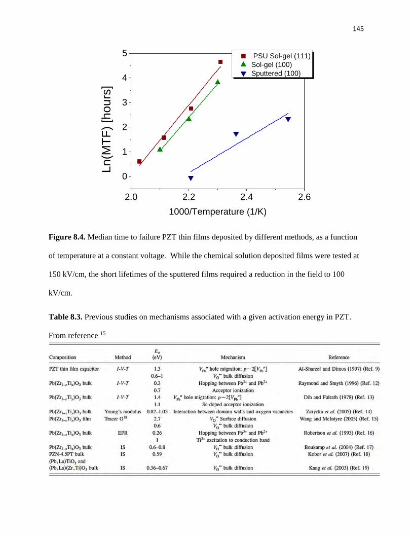
145
2.0 2.2 2.4 2.6
0
1
2
3
4
5
Ln(M
TF) [
hour
s]
1000/Temperature (1/K)
PSU Sol-gel (111)Sol-gel (100)Sputtered (100)
Figure 8.4. Median time to failure PZT thin films deposited by different methods, as a function
of temperature at a constant voltage. While the chemical solution deposited films were tested at
150 kV/cm, the short lifetimes of the sputtered films required a reduction in the field to 100
kV/cm.
Table 8.3. Previous studies on mechanisms associated with a given activation energy in PZT.
From reference 15
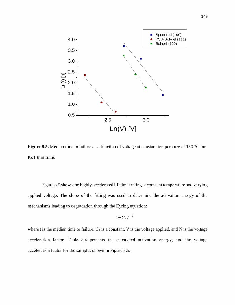
146
Figure 8.5. Median time to failure as a function of voltage at constant temperature of 150 °C for
PZT thin films
Figure 8.5 shows the highly accelerated lifetime testing at constant temperature and varying
applied voltage. The slope of the fitting was used to determine the activation energy of the
mechanisms leading to degradation through the Eyring equation:
NTVCt
where t is the median time to failure, CT is a constant, V is the voltage applied, and N is the voltage
acceleration factor. Table 8.4 presents the calculated activation energy, and the voltage
acceleration factor for the samples shown in Figure 8.5.
2.5 3.00.5
1.0
1.5
2.0
2.5
3.0
3.5
4.0Sputtered (100)PSU-Sol-gel (111)Sol-gel (100)
Ln(t)
[h]
Ln(V) [V]
147
The voltage acceleration factors determined from the Eyring equation were incongruent
with established models for possible conduction mechanisms (See Table 8.5). Amongst these
possible conduction mechanisms, none have a fourth or fifth order polynomial relationship
between the electric field and the leakage current in the material. This indicates that the voltage
acceleration model derived from the Eyring equation is unphysical, which calls into question the
assumption made about the mechanisms of failure within these films. In order to reliably predict
lifetime for PZT thin films, a new model based on the physical mechanisms of failure for that
material is necessary. This has been done for bulk BaTiO3 ceramic dielectrics.18 Here, the
applicability of the new model to thin films are necessary is explored.
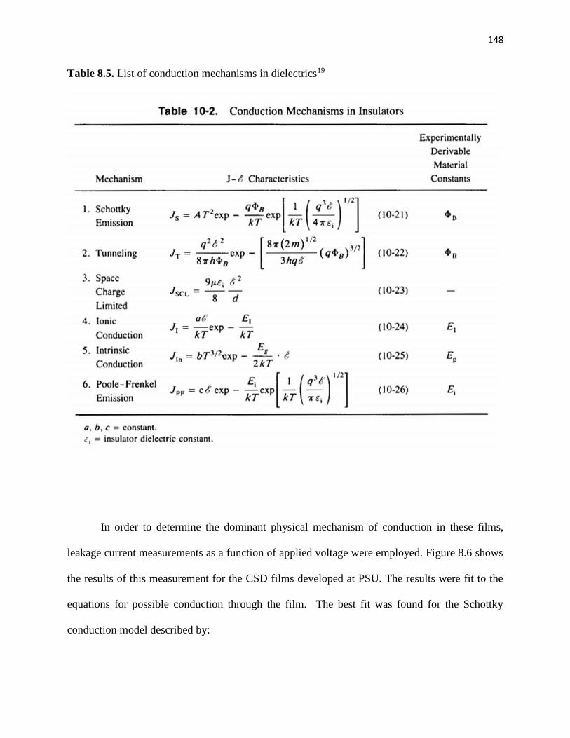
148
Table 8.5. List of conduction mechanisms in dielectrics19
In order to determine the dominant physical mechanism of conduction in these films,
leakage current measurements as a function of applied voltage were employed. Figure 8.6 shows
the results of this measurement for the CSD films developed at PSU. The results were fit to the
equations for possible conduction through the film. The best fit was found for the Schottky
conduction model described by:
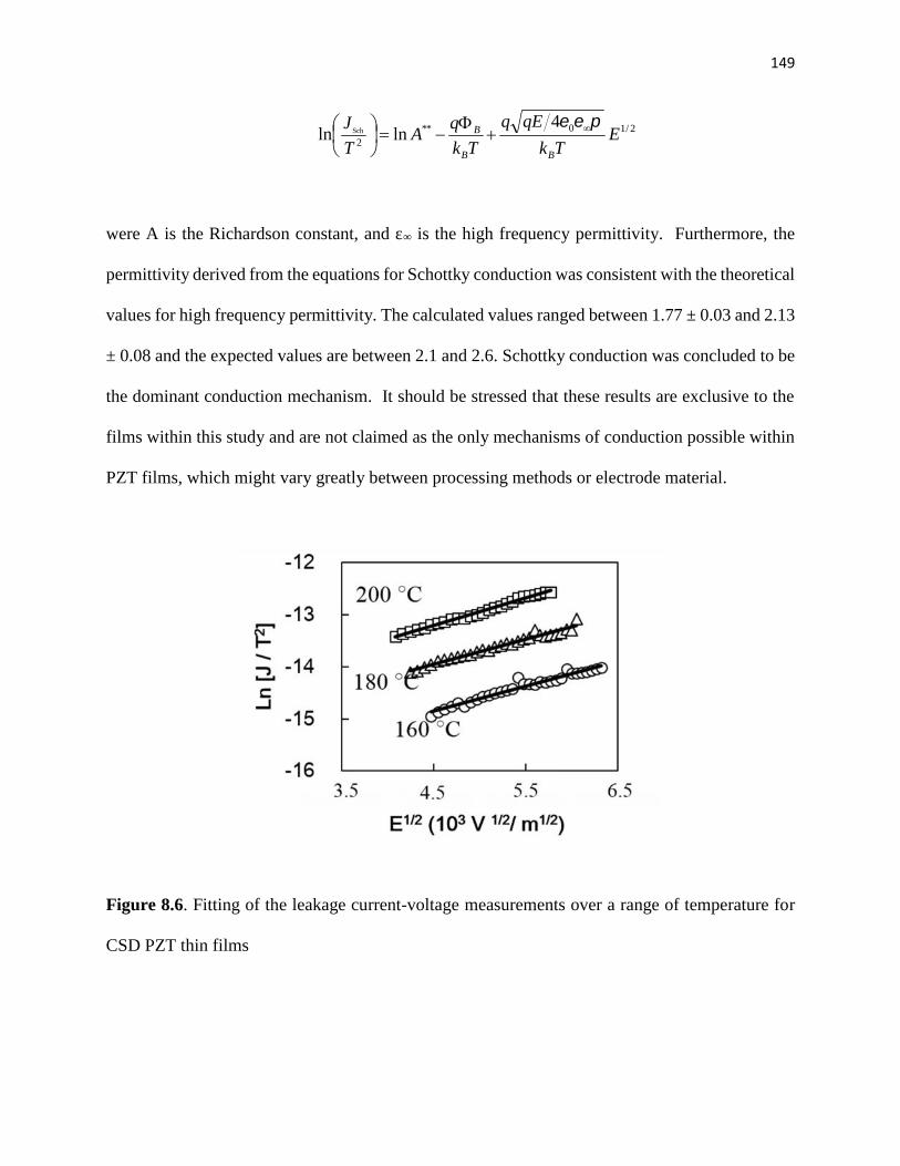
149
2/10**2
4lnln Sch E
Tk
qEq
Tk
qA
T
J
BB
B
were A is the Richardson constant, and ε∞ is the high frequency permittivity. Furthermore, the
permittivity derived from the equations for Schottky conduction was consistent with the theoretical
values for high frequency permittivity. The calculated values ranged between 1.77 ± 0.03 and 2.13
± 0.08 and the expected values are between 2.1 and 2.6. Schottky conduction was concluded to be
the dominant conduction mechanism. It should be stressed that these results are exclusive to the
films within this study and are not claimed as the only mechanisms of conduction possible within
PZT films, which might vary greatly between processing methods or electrode material.
Figure 8.6. Fitting of the leakage current-voltage measurements over a range of temperature for
CSD PZT thin films
150
Using the assumptions of constant critical charge to failure (borrowed from the
semiconductor industry20) and the equations for Schottky conduction new models for reliability
were developed. The new fitting equations were derived through the following process:
= ==
= ( ) ( )
= ( ) ( )( )
Constant voltage
= ( )= − += 4
Constant temperature
==
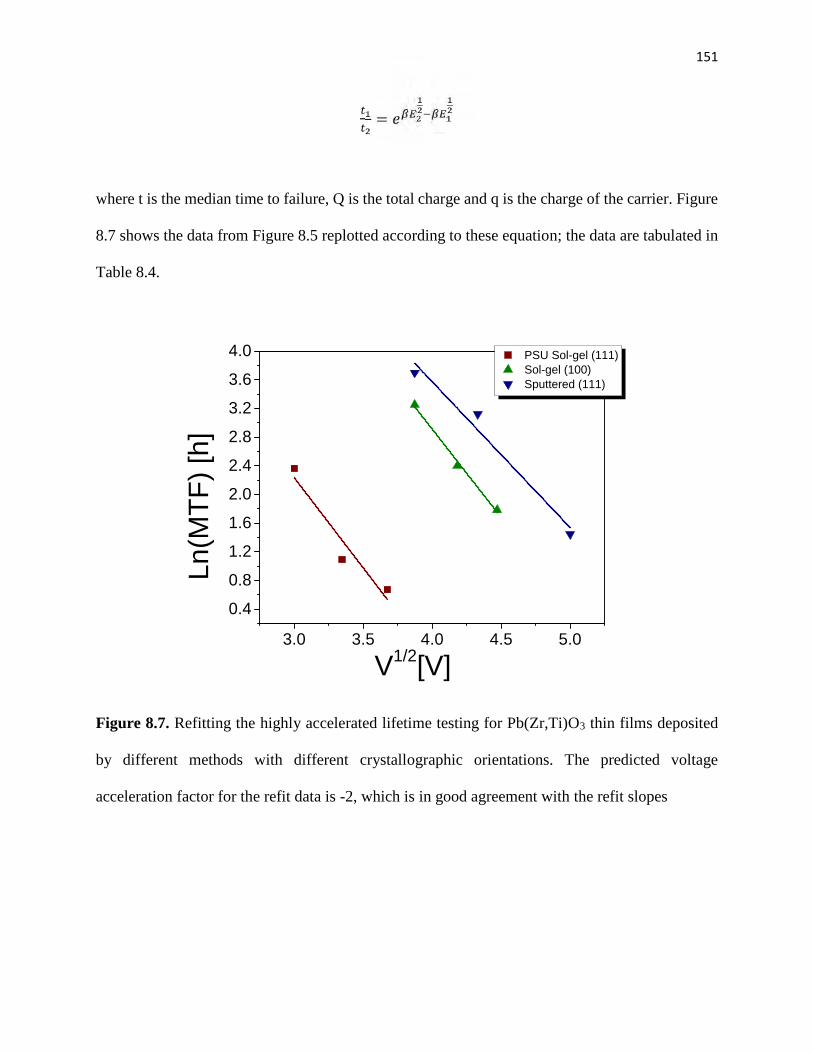
151
=where t is the median time to failure, Q is the total charge and q is the charge of the carrier. Figure
8.7 shows the data from Figure 8.5 replotted according to these equation; the data are tabulated in
Table 8.4.
3.0 3.5 4.0 4.5 5.0
0.4
0.8
1.2
1.6
2.0
2.4
2.8
3.2
3.6
4.0 PSU Sol-gel (111) Sol-gel (100) Sputtered (111)
Ln(M
TF) [
h]
V1/2[V]
Figure 8.7. Refitting the highly accelerated lifetime testing for Pb(Zr,Ti)O3 thin films deposited
by different methods with different crystallographic orientations. The predicted voltage
acceleration factor for the refit data is -2, which is in good agreement with the refit slopes
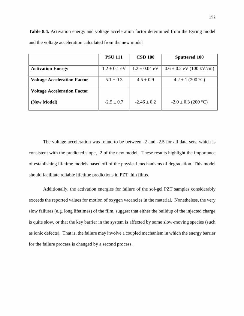
152
Table 8.4. Activation energy and voltage acceleration factor determined from the Eyring model
and the voltage acceleration calculated from the new model
PSU 111 CSD 100 Sputtered 100
Activation Energy 1.2 ± 0.1 eV 1.2 ± 0.04 eV 0.6 ± 0.2 eV (100 kV/cm)
Voltage Acceleration Factor 5.1 ± 0.3 4.5 ± 0.9 4.2 ± 1 (200 °C)
Voltage Acceleration Factor
(New Model) -2.5 ± 0.7 -2.46 ± 0.2 -2.0 ± 0.3 (200 °C)
The voltage acceleration was found to be between -2 and -2.5 for all data sets, which is
consistent with the predicted slope, -2 of the new model. These results highlight the importance
of establishing lifetime models based off of the physical mechanisms of degradation. This model
should facilitate reliable lifetime predictions in PZT thin films.
Additionally, the activation energies for failure of the sol-gel PZT samples considerably
exceeds the reported values for motion of oxygen vacancies in the material. Nonetheless, the very
slow failures (e.g. long lifetimes) of the film, suggest that either the buildup of the injected charge
is quite slow, or that the key barrier in the system is affected by some slow-moving species (such
as ionic defects). That is, the failure may involve a coupled mechanism in which the energy barrier
for the failure process is changed by a second process.
153
8.4 Supplementary Measurements: Voltage Contrast Microscopy and Optical Microscopy
Voltage contrast microscopy is another method which can be used to characterize the
reliability and degradation of a thin film device. Voltage contrast microscopy investigates the real
time degradation of a material through the application of voltage during scanning electron
microscopy. Shown in Figure 8.8 are two areas of a PZT thin film device under 30 Volts. No post
processing changes were made to the contrast of these images. These films were under voltage
for 4.5 hours prior to the taking of these images. Over this time the electric field was observed to
bleed into the dielectric within certain regions as indicated by the increased contrast in degraded
areas. Over time the intensity of the contrast would increase, suggesting injected charge, until
failure occurred with the complete destruction of the electrode area. Due to the fact that
information provided by voltage contrast microscopy is limited to the surface of the sample, this
method would be most beneficially employed for interdigitated electrodes or features with tight
line spacing.
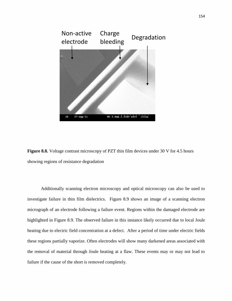
154
Figure 8.8. Voltage contrast microscopy of PZT thin film devices under 30 V for 4.5 hours
showing regions of resistance degradation
Additionally scanning electron microscopy and optical microscopy can also be used to
investigate failure in thin film dielectrics. Figure 8.9 shows an image of a scanning electron
micrograph of an electrode following a failure event. Regions within the damaged electrode are
highlighted in Figure 8.9. The observed failure in this instance likely occurred due to local Joule
heating due to electric field concentration at a defect. After a period of time under electric fields
these regions partially vaporize. Often electrodes will show many darkened areas associated with
the removal of material through Joule heating at a flaw. These events may or may not lead to
failure if the cause of the short is removed completely.
Non-activeelectrode
Chargebleeding Degradation
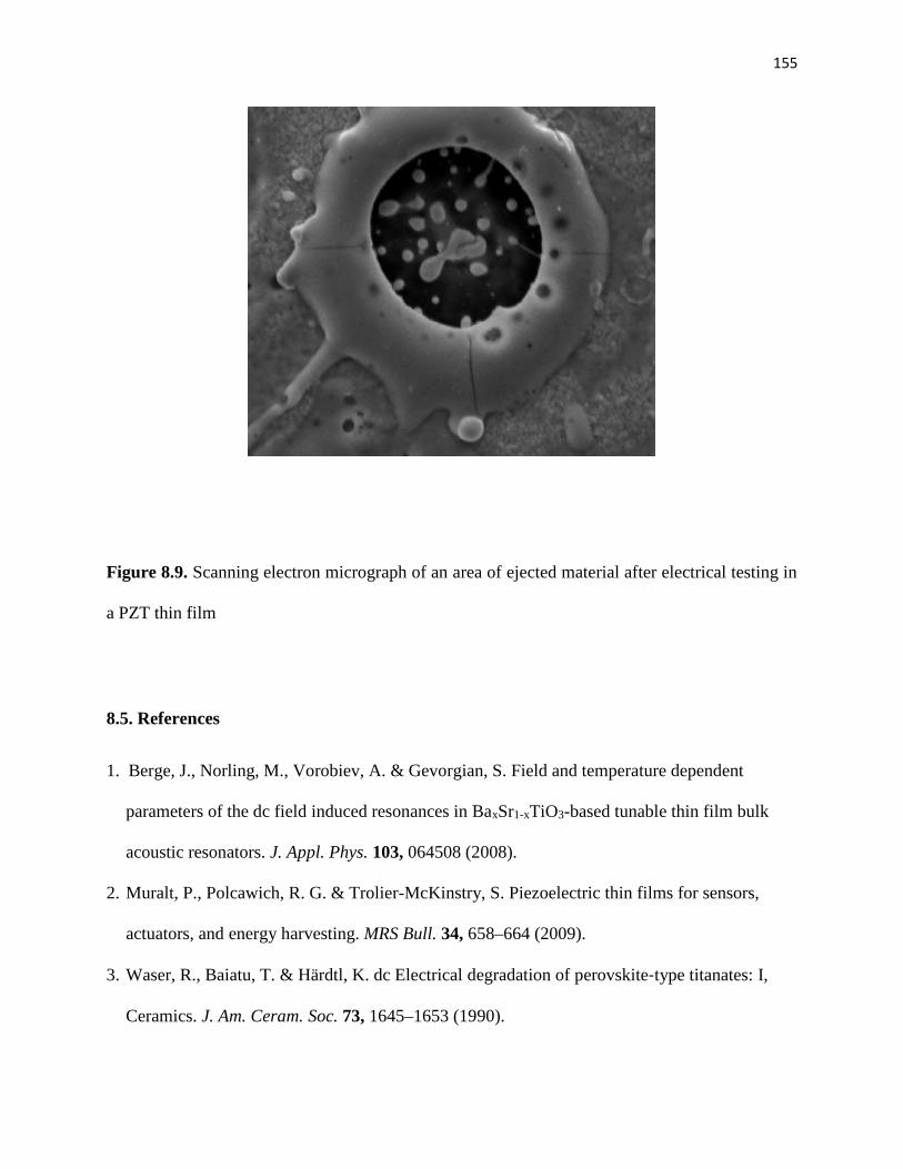
155
Figure 8.9. Scanning electron micrograph of an area of ejected material after electrical testing in
a PZT thin film
8.5. References
1. Berge, J., Norling, M., Vorobiev, A. & Gevorgian, S. Field and temperature dependent
parameters of the dc field induced resonances in BaxSr1-xTiO3-based tunable thin film bulk
acoustic resonators. J. Appl. Phys. 103, 064508 (2008).
2. Muralt, P., Polcawich, R. G. & Trolier-McKinstry, S. Piezoelectric thin films for sensors,
actuators, and energy harvesting. MRS Bull. 34, 658–664 (2009).
3. Waser, R., Baiatu, T. & Härdtl, K. dc Electrical degradation of perovskite‐type titanates: I,
Ceramics. J. Am. Ceram. Soc. 73, 1645–1653 (1990).
156
4. Al‐Shareef, H. N. & Dimos, D. Leakage and reliability characteristics of lead zirconate
titanate thin‐film capacitors. J. Am. Ceram. Soc. 80, 3127–3132 (1997).
5. Bouyssou, E., R. Jérisian, N. Cézac, P. Leduc, G. Guégan, and C. Anceau, Wafer level
reliability and leakage current modeling of PZT capacitors. Mater. Sci. Eng. B 118, 28–33
(2005).
6. Yang, Y. S., Lee, S. J., Kim, S. H., Chae, B. G. & Jang, M. S. Schottky barrier effects in the
electronic conduction of sol–gel derived lead zirconate titanate thin film capacitors. J. Appl.
Phys. 84, 5005–5011 (1998).
7. Juan, T. P.-C., Chen, S. & Lee, J. Y. Temperature dependence of the current conduction
mechanisms in ferroelectric Pb(Zr0.53,Ti0.47)O3 thin films. J. Appl. Phys. 95, 3120–3125
(2004).
8. Polcawich, R. G., C. Feng, P. Vanatta, R. Piekarz, S. Trolier-McKinstry, M. Dubey, and M.
Ervin, Highly accelerated lifetime testing (HALT) of lead zirconate titanate (PZT) thin films.
Proceedings of the 2000 12th IEEE International Symposium on Applications of
Ferroelectrics, 2000. ISAF 2000 1, 357–360 vol. 1 (IEEE, 2000).
9. Polcawich, R. G., Moses, P. J. & Trolier-McKinstry, S. AC and DC electrical stress reliability
of piezoelectric lead zicronate titanate (PZT) thin films. Presented at Microelectronics 1999.
3906, 227 (1999).
10. Nagaraj, B., Aggarwal, S., Song, T. K., Sawhney, T. & Ramesh, R. Leakage current
mechanisms in lead-based thin-film ferroelectric capacitors. Phys. Rev. B 59, 16022–16027
(1999).
157
11. Chen, J., Chen, H. & Lee, J. Y. An investigation on the leakage current and time dependent
dielectric breakdown of ferroelectric lead–zirconate–titanate thin film capacitors for memory
device applications. Appl. Phys. Lett. 69, 4011–4013 (1996).
12. Sudhama, C., A. Campbell, P. D. Maniar, R. E. Jones, R. Moazzami, C. J. Mogab, and J. C.
Lee, A model for electrical conduction in metal-ferroelectric-metal thin film capacitors. J.
Appl. Phys. 75, 1014–1022 (1994).
13. Mihara, T. & Watanabe, H. Electronic Conduction Characteristics of Sol-Gel Ferroelectric
Pb(Zr0.4Ti0.6)O3 Thin-Film Capacitors: Part I. Jpn. J. Appl. Phys. 34, 5664 (1995).
14. Dimos, D., Schwartz, R. W. & Lockwood, S. J. Control of leakage resistance in Pb(Zr,Ti)O3
thin films by donor doping. J. Am. Ceram. Soc. 77, 3000–3005 (1994).
15. Zhao, S., Zhang, S. J., Liu, W., Donnelly, N. J., Xu, Z., Randall, C. A., Time dependent dc
resistance degradation in lead-based perovskites: 0.7 Pb(Mg1/3Nb2/3)O3−0.3 PbTiO3. J. Appl.
Phys. 105, 053705 (2009).
16. Masuda, Y. & Nozaka, T. Investigation into electrical conduction mechanisms of
Pb(Zr,Ti)O3 thin-film capacitors with Pt, IrO2 and SrRuO3 top electrodes. Jpn. J. Appl. Phys.
43, 6576 (2004).
17. Stolichnov, I., A. Tagantsev, N. Setter, S. Okhonin, P. Fazan, J. S. Cross, M. Tsukada, A.
Bartic& D. Wouters, Constant-current study of dielectric breakdown of Pb(Zr,Ti)O3
ferroelectric film capacitors. Integr. Ferroelectr. 32, 737–746 (2001).
18. Randall, C. A.,R. Maier, W. Qu, K. Kobayashi, K. Morita, Y. Mizuno, N. Inoue and T.
Oguni, Improved reliability predictions in high permittivity dielectric oxide capacitors under
high dc electric fields with oxygen vacancy induced electromigration. J. Appl. Phys. 113,
014101 (2013).
158
19. Ohring M., The Materials Science of Thin Films. Academic Press, London, 1992.
20. Lampert, M.. Current Injection in Solids. Academic Press, London, 1970.
159
Chapter 9
Conclusions and Future Work
9.1 Conclusions
This chapter reviews the major conclusions from the work described in this thesis.
Recommendations for future work are provided in light of these results.
9.1.1 Residual Ferroelectricity in BST Tunable Dielectrics
Rayleigh behavior as a function of temperature was used to track the ferroelectric behavior
of BST materials through the ferroelectric to paraelectric transition temperature. The irreversible
Rayleigh parameter serve as a metric for the presence of ferroelectricity because this response is
dependent on the presence of domain walls, cluster boundaries or phase boundaries. The Rayleigh
results were found to be in good agreement with the measured minor polarization-electric field
hysteresis loops. The logarithmic decay of the frequency dependence of the Rayleigh behavior was
consistent with other ferroelectric systems1 and the Rayleigh behavior was further corroborated
through optical second harmonic generation. In the future it would be important to address the
impacts of inhomogeneous electric fields in the materials with interdigitated top electrodes on the
Rayleigh response and tunability in these materials.
From the Rayleigh analysis, residual ferroelectricity –a persistent ferroelectric response
above the global phase transition temperature– was observed in BST ceramics and thin films
processed by different methods. While all of the measured materials exhibited residual
160
ferroelectricity, the temperature extent varied greatly between materials processed by different
methods. A-site chemical inhomogeneity was found to promote residual ferroelectricity.
This study has shown ferroelectric based loss persists well beyond the expected transition
temperature in many BST materials. In order to avoid ferroelectric based loss the transition
temperature should be suppressed, by varying the barium to strontium ratio, in equal measure to
the temperature extent of the residual ferroelectricity. It is also suggested that ferroelectric
measurements of tunable dielectric material be routinely made using Rayleigh analysis. Rayleigh
analysis provides an indication of ferroelectricity which is not possible through polarization-
electric field hysteresis loops which is what is currently most often reported.
9.1.2. Residual Ferroelectricity and Flexoelectricity
Residual ferroelectricity is observed in barium strontium titanate ceramics 30°C above the
global phase transition temperature, in the same temperature range in which anomalously large
flexoelectric coefficients are reported. The application of a strain gradient in this temperature range
leads to strain gradient-induced poling, or flexoelectric poling, enhancing the flexoelectric
response. Flexoelectric poling was observed by the development of a remanent polarization in
flexoelectric measurements upon the removal of the applied strain gradient. Additionally, an
induced d33 piezoelectric response was observed in samples after the removal of the applied strain
gradient, indicating that the polarization was realigned during flexoelectric measurements.
Flexoelectric poling lead to the production of an internal bias of 9 kV/m. It is concluded that
residual ferroelectric response considerably enhances the observed flexoelectric response.
161
9.1.3. Electric Field Induced Piezoelectricity in BST thin films
Metrology was designed, developed and calibrated for the measurement of the e31,f
piezoelectric coefficient as a function of applied electric field and strain. This allowed for direct
measurements of the field-induced piezoelectric response for Ba0.7Sr0.3TiO3 (70:30) and
Ba0.6Sr0.4TiO3 (60:40) thin films on MgO and silicon. The DC electric field dependence of the
permittivity (tunability), and the dielectric non-linearity were also characterized. The relative
dielectric tunabilities for the 70:30 and 60:40 composition on MgO were 83% and 70%
respectively, with a dielectric loss of less than 0.011 and 0.004 at 100 kHz. A linear increase in
induced piezoelectricity with field to –3.0 C/m2 and –1.5 C/m2 at 110 kV/cm was observed in
60:40 BST on MgO and 70:30 BST on Si. Large and hysteretic piezoelectric and tuning responses
were observed in the 70:30 BST thin films on MgO. This was consistent with the irreversible
Rayleigh behavior, indicating a ferroelectric contribution to the piezoelectric and dielectric
response 40°C above the global paraelectric transition temperature. Field-induced piezoelectricity
was observed both in films on substrates which should impart tensile or compressive stress. This
information should enable advancements in tunable dielectric components through the removal of
piezoelectric resonance-based loss mechanisms. Further work in investigating the piezoelectric
and electrostricitive response could be done through an investigation of the electromechanical
response at odd or even higher order harmonics.
9.2 Future Work
162
9.2.1. Characterization of Residual Ferroelectricity in Materials for Flexoelectric
Applications
Chapter 7 discusses the relationship between residual ferroelectricity and flexoelectricity
(specifically the flexocoupling factor) in BST. Flexocoupling factors which are orders of
magnitude higher than what was theoretically predicted (1-10V) have been observed in BST.2
Residual ferroelectricity, as measured through Rayleigh analysis, is examined as a mechanism
behind the enhanced flexocoupling in BST.
Enhanced flexocoupling is not exclusive to BST, in fact many ferroelectric perovskite
materials exhibit anomalously large flexocoupling coefficients. The last column of Table 9.1
shows the flexocoupling factor, f, for a series of ferroelectric perovskites.2 The available data
suggest that flexocoupling coefficients beyond what is theoretically predicted are observed in all
perovskites which can become ferroelectric. In contrast to this, in perovskite materials with similar
structures but lacking ferroelectricity, such as strontium titanate, the flexocoupling response is
within the predicted range of 1-10 V.3
There have been as of yet few attempts to study the mechanisms of enhanced flexocoupling
in ferroelectric perovskites. Narvaez and Catalan have shown a correlation between the onset of
nano-polar regions and enhanced flexoelectric response in a relaxor ferroelectric.4 This supports
the idea that ferroelectricity impacts the flexoelectric response, but does not account for the
nominally normal ferroelectric perovskites with enhanced flexocoupling.
The work described within this thesis shows a correlation between the onset of residual
ferroelectricity and enhanced flexcoupling in BST. Extending the study of residual
ferroelectricity to other materials for flexoelectric applications, such as barium titanate, lead
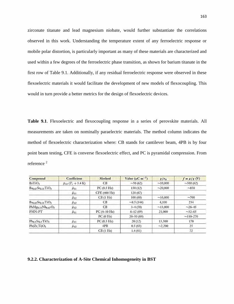
163
zirconate titanate and lead magnesium niobate, would further substantiate the correlations
observed in this work. Understanding the temperature extent of any ferroelectric response or
mobile polar distortion, is particularly important as many of these materials are characterized and
used within a few degrees of the ferroelectric phase transition, as shown for barium titanate in the
first row of Table 9.1. Additionally, if any residual ferroelectric response were observed in these
flexoelectric materials it would facilitate the development of new models of flexocoupling. This
would in turn provide a better metrics for the design of flexoelectric devices.
Table 9.1. Flexoelectric and flexocoupling response in a series of perovskite materials. All
measurements are taken on nominally paraelectric materials. The method column indicates the
method of flexoelectric characterization where: CB stands for cantilever beam, 4PB is by four
point beam testing, CFE is converse flexoelectric effect, and PC is pyramidal compression. From
reference 2
9.2.2. Characterization of A-Site Chemical Inhomogeneity in BST
164
In chapter 6, residual ferroelectricity in BST was investigated with respect to A-site
chemical inhomogeneity. As measured by electron energy loss spectroscopy, EELS, there is a
significant difference between samples with narrow and broad temperature dependent Rayleigh
behavior, with inhomogeneous samples exhibiting broader temperature dependences. Now that
this chemical inhomogeneity has been observed, the next step to mitigating residual ferroelectric
based loss requires an understanding of the driving forces for disordering in the BST system.
Understanding the mechanisms which control the length scales of ordering in this material could
provide insight into methods to regulate chemical homogeneity and reduce ferroelectric loss.
Further information could be inferred through an investigation of variations in the full width half
maximum of the x-ray diffraction patterns taken on the samples used in this study. Additionally,
further investigations into the time and temperature dependence of the Rayleigh response would
provide information about aging and degradation from which inference could be made into the
structure and movement of the domains, cluster or phase boundaries. A direct measurement of the
order could also be possible through the application of transmission electron microscopy, as has
previously been used in the work of Bursill to identify ordered clusters in barium titanate.5
Further establishing a causal relationship between A-site chemical inhomogeneity and
residual ferroelectricity requires a thorough measure of the local chemical distribution. The EELS
method relies on variations in the barium to titanium ratio to infer differences between the barium
to strontium ratios. This assumes that barium titanate is a line compound. However, it is known
that a finite solid solution window exists with variable A:B ratios.6 Furthermore, thin films are not
necessarily in thermodynamic equilibrium, 7,8 which could further change the A:B ratio in the
single phase material. Energy dispersive spectroscopy, EDS, would allow for a more direct
characterization of the local scale barium to strontium ratio.9 EDS measurements on barium
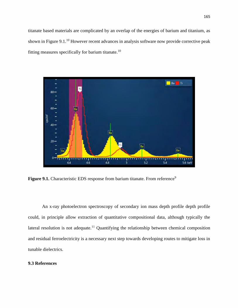
165
titanate based materials are complicated by an overlap of the energies of barium and titanium, as
shown in Figure 9.1.10 However recent advances in analysis software now provide corrective peak
fitting measures specifically for barium titanate.10
Figure 9.1. Characteristic EDS response from barium titanate. From reference9
An x-ray photoelectron spectroscopy of secondary ion mass depth profile depth profile
could, in principle allow extraction of quantitative compositional data, although typically the
lateral resolution is not adequate.11 Quantifying the relationship between chemical composition
and residual ferroelectricity is a necessary next step towards developing routes to mitigate loss in
tunable dielectrics.
9.3 References
166
1. Taylor, D. V. & Damjanovic, D. Evidence of domain wall contribution to the dielectric
permittivity in PZT thin films at sub-switching fields. J. Appl. Phys. 82, 1973–1975 (1997).
2. Zubko, P., Catalan, G. & Tagantsev, A. K. Flexoelectric effect in solids. Annu. Rev. Mater.
Res. 43, 387–421 (2013).
3. Zubko, P., Catalan, G., Buckley, A., Welche, P. R. L. & Scott, J. F. Strain-Gradient-Induced
polarization in SrTiO3 single crystals. Phys. Rev. Lett. 99, 167601 (2007).
4. Narvaez, J. & Catalan, G. Origin of the enhanced flexoelectricity of relaxor ferroelectrics.
Appl. Phys. Lett. 104, 162903 (2014).
5. Bursill, L. A. & Lin, P. J. Microdomains observed at the ferroelectric/paraelectric phase
transition of barium titanate. Nature 311, 550–552 (1984).
6. Lee, S., Randall, C. A. & Liu, Z.-K. Modified phase diagram for the barium oxide–titanium
dioxide system for the ferroelectric barium titanate. J. Am. Ceram. Soc. 90, 2589–2594
(2007).
7. Schwartz, R. W. Chemical solution deposition of perovskite thin films. Chem. Mater. 9,
2325–2340 (1997).
8. Lange, F. F. Chemical solution routes to single-crystal thin films. Science 273, 903–909
(1996).
9. Joshi, U. A. & Lee, J. S. Template-Free hydrothermal synthesis of single-crystalline barium
titanate and strontium titanate nanowires. Small 1, 1172–1176 (2005).
10. AZtec TruMap. EDS Software. (Oxford Insutrments, 2013).
11. Stickle, William F., Peter E. Sobol, and Kenneth D. Bomben. Handbook of X-ray
photoelectron spectroscopy. Vol. 40. Eden Prairie, MN: Perkin Elmer, 1992.
VITA
Lauren Garten
Lauren Garten was born in Utica, MI on June 23, 1986. In 2004 she began studying music
performance/education at the Missouri State University. For two years she played in a number of
music ensembles and toured the country with a drum and bugle corps. Then after a long battle with
severe stage fright, she decided to give up her career in music and follow her passion for science
(and hoped to never have to perform in front of a crowd again). She transferred to the University
of Missouri-Rolla, and graduated with a bachelors degree in ceramic engineering in December
2008. Then in January 2009 she started her graduate career at the Pennsylvania State University.
In 2011 she transferred out of the program to work as a technician for Dr. Meyer at the Applied
Research Laboratory and for Dr. Trolier-McKinstry at the Materials Research Laboratory. She
then restarted her graduate career with Dr. Trolier-McKinstry and under her guidance went on to
complete her graduate work.