Embed Size (px)
Citation preview
THE INVESTIGATION ON THE FACTORS THAT AFFECT THE RESISTANCE
OF DRAIN-TO-SOURCE IN SEMICONDUCTOR PACKAGING
CHUA KING LEE
THESIS SUBMITTED IN PARTIAL FULFILMENT FOR THE DEGREE OF
MASTER OF SCIENCE
FAKULTI KEJURUTERAAN ELEKTRIK, ELEKTRONIK DAN SISTEM
UNIVERSITI KEBANGSAAN MALAYSIA
BANGI
2004
DECLARA TION
I hereby declare that the work in this thesis is my own except for quotations and summaries which have been duly acknowledged.
1 February 2004
'IDlsertasi ini tclah diluluskan selbla.g;'i:l~a~Se;~~~~e::~~gtan darlpada syara~ mempero ell J <-
(Mikroelcktronlk)
I'V ......... ~~ Kctua Jabatan
Tarilili ........ .-~!)..~: i .,.;;;. ••••• n ••••••• ••••••••••
PCnYCI~r J 'lrnrlkb.<J!1 ... ? .. ~1 (
11
III
APPRECIA TION
With grateful to God in giving me good health and perseverance to complete my project smoothly and on time. This project has been successfully completed under my effort and assistance from ON Semiconductor.
I would like to take this opportunity to express my deepest gratitude and thanks to :-
1. Mr Ibrahim as my supervisor who has been given me advice and guidance in my thesis writing.
ii. Mr Ghazali Omar as my co-supervisor who has been very supportive in guiding me while running this project at his working place.
iii. S. K. Yong; head of Failure Analysis Department who has been spending his time to train, guide and allow me to use the equipments during the runs of project in his department.
iv. H. K. Lee from Top Department who has been sharing his ideas and thoughts with me in conducting this project.
v. All technicians in Failure Analysis Department. VI. My family and friends who care and support me during the runs of this
project.
Thank you.
CHUA KING LEE Jabatan Kejuruteraan Elektrik, Elektronik Dan Sistem Fakulti Kejuruteraan Universiti Kebangsaan Malaysia
IV
ABSTRACT
The objectives of the project is to investigate the characteristics contact resistance of the silicon lead-frame interface using ECA die attach materials, and to evaluate the factors contributing to the increase of interface resistively in semiconductor packaging. This project was done at ON Semiconductor where silver-filler epoxybased adhesive chips were investigated.
Tektronix 370B Programmable Curve Tracer with picoprobing is used to measure RoN of the chips. Nondestructive techniques such as X-ray and SAM used to examine internal defect and cross sectional analysis was done using SEM.
Few factors were found affect RoN. Those factors are capacitance due to trap charges during fabrication, supply voltage, thermal management of the package, delamination between die attachments, thickness of the epox)' and copper dioxide of the lead-frame.
v
ABSTRAK
Objektif projek adalah untuk mengkaji ciri-ciri rintangan sentuh bagi antaramuka leadframe-silikon dengan menggunakan bahan lekat die dan menilai fak-tor-faktor berkaitan kepada peningkatan rintangan bungkllsan semikondukior. Projek ini dijalankan di ON Semiconductor dan cip silver-filler epo.\)'-based adhesive dikajikan.
Tektronix 370B Programmable Cun'e Tracer dengan picoprobing digunakan untuk mengukur RON cip. Teknik nondestructive seperti X-ray dan SAM digunakan untuk memeriksa kerosakan dalaman dan analisis keratan rentas dilakukan dengan menggunakan SEM.
Terdapat beberapa fak-tor didapati mempengaruhi RoN. Fak1or-fak1or tersebut adalah kapasitan yang disebabkan oleh cas terperangkap semasa fabrikasi, sumber voltan, pengurusan term a pad a bungkusan, delamination antara perlekatan die, ketebalan eposi dan karbon dioksida bagi lead-frame.
DECLARATION
APPRECIATION
ABSTRACT
ABSTRAK
CONTENT
TABLE LIST
FIGURE LIST
SYMBOL LIST
CHAPTER!
1.1
1.2
1.3
CHAPTERll
2.1
2.2
2.3
CONTENT
INTRODUCTION
Background
Objective
Organization Of This Dissertation
LITERATURE REVIEW
Semiconductor Packaging
Thin Film Transistor Technologies
Die Attachment Techniques
2.3.1 Wire Bonding 2.3.2 Tape-Automated Bonding 2.3.3 Solder Bump Bonding
VI
Page
11
III
IV
V
VI
IX
IX
Xl
13
14
14
16
18
20
20 20 21
V11
2.4 Die Attachment Process 21
2.5 Electrically Conductive Adhesives 22
2.6 Drain-To-Source Resistance 25
2.7 The Importance Of RaN In Packaging 27
CHAPTERID METHODOLOGY
3.1 Material 29
3.2 Resistance Measurement 30
3.3 Internal Imaging Analysis 32
3.4 Thermal Management 34
3.5 Cross Sectional Analysis 34
3.6 Scanning Electron Microscopy (SEM) 35
CHAPTER IV RESULT AND DISCUSSION
4.1 Introduction 37
4.2 RaN Measurement Result 37
4.3 Varying Input Voltage 40
4.4 Thermal Management 42
4.5 Delamination 43
4.6 Thickness OfEpoxl' 46
4.7 Copper Dioxide 47
CHAPTER V SUMMARY AND CONCLUSIONS 49
REFERENCE 51
APPENDIX A
RON Value for 10 units sample Device A 53
VlIl
APPENDIXB
RoN Value for 10 units sample Device B 54
APPENDIXC
RoN Value When Tested In Different Temperature 55
APPENDIXD
Electrical Conduction Models for Isotropically Conductive Adhesive Joints 57
APPENDIXE
Materials Characterization, Conduction Development and Curing Effects on Reliability of Isotropically Conductive Adhesive 63
APPENDIXF
Development of High Conductivity Lead (Pb)-Free Conducting Adhesive 72
IX
TABLE LIST
Table No. Page
4.1 Standard Deviation for Device A and Device B 39
4.2 Test Result for Varying Input Voltage on Device A 40
4.3 Test Result for Varying Input Voltage on Device B 41
4.4 RoN Measurement for Chip With and Without Die Attach 42 Package (DAP)
4.5 Result RoN when Baked in Different Temperature for 4 hours 43
4.6 Comparison RoN Value for Device A and Device B 46
FIGURE LIST
Figure No. Page
2.1 Basic process of semiconductor packaging 16
2.2 Moisture absorption in the encapsulation can cause 17 downstream problems such as cracking during assembly
2.3 A typical a-Si:H thin film transistor (TFT) structure 18
2.4 A polysilicon TFT structure 19
2.5 Die Attachment Process 22
2.6 Alignment of filler particles before and after cure 23
2.7 On resistance or resistance drain-to-source 25
2.8 N-channel MOSFET CnMOS) 25
3.1 Bonding diagram SOML5208 29
\
3.2 The internal view of device b\' X-ra\' ':;11 - -
3.3 Tektronix 370B Programmable Cur;e Tracer .:; 1
3.4 (a) I-V characteristic of breakdown \'oJtage 31 (b) Characteristic of short ci rcuit
3.5 Principles of the acoustic microscope _" -"I
3.6 Scanning Electron Microscopy 3h
4.1 Graph Resistance versus Unit Chips Assembly at 3~
Different Wafer Fabrication
4.2 Terminology for the charges associated with thermally 3q
oxidized silicon
4.3 Scanning Acoustic Microscopy for chip that baked ~~
in different temperature for 4 hours
4.4 Scanning Electron Microscopy \\;th resolution 750x ~~
4.5 Scanning Electron Microscopy with resolution 7500x .) :'
4.6 Internal View of Epoxy Layer for Device A and De\'icc .)(,
B by Cross Sectional Analysis
4.7 Cracks At Cu-AI Interface On The Footprint Chip ~7
~n ACA Al AMLCD a-Si:H BVDSS COB COF COG Cox CTE Cu Cu20 DAP DCA ECA FIB FPD I I/O IC ICA ID IDSS L MCM MOS MOSFET
+ n Pb PC PCB PDA Qr Qit Qrn Qot R RoN SAM/SAT SEM Si02
Sn TAB
SYMBOL LIST
Ohm Electron Mobility Anisotropic Conductive Adhesive Aluminum Active-matrix liquid-crystal display Hydrogenated Amorphous Silicon / Polycrystalline Silicon Breakdown Voltage Chip-on-Board Chip-on-Flex Chip-on-Glass Oxide Capacitance Coefficient Thermal Expansion Copper Copper Oxide Die Attach Package Direct Chip Attachment Electrical Conductive Adhesive Focused Ion Bean Flat-panel displays Current Input/Output Integrated Circuit Isotropic Conductive Adhesive Drain (Source) Current Drain Source Short Current Length Multi-Chip Module Metal Oxide Silicon Metal Oxide Semiconductor Field Effect Transistor High Doping Type n Plumbum Personal Computer Printed Circuit Board Personal Digital Assistant Fixed Charge Interface-Trapped Charges Mobile Tonic Charges Oxide-Trapped Charges Resistance Drain-to-Source resistance Scanning Acoustic Microscopy Scanning Electron Microscopy Silicon Dioxide Lead Tape-Automated Bonding
XI
TFT Tgs V Vos Vo VGS(th)NT VIN Vs W
Thin-film transistor Glass Transition Temperature Voltage Drain Source Voltage Gate Voltage Threshold voltage Input Voltage Source Voltage Width
Xli
CHAPTER I
INTRODUCTION
1.1 BACKGROUND
Semiconductor packaging is a process used to assemble IC devices in electronic
packages which provides the interconnection from the IC chip to the printed circuit
board (PCB). It provides electrical connection of the chips with wires to distribute
signals and power, remove the heat generated by the circuits and provides them with
physical support and environmental protection. It plays an important role in
determining the performance, cost and reliability of the system.
For many decades, the semiconductor packaging was well served by solders
lead, Pb. Tin/lead, SnPb, eutectic solder has become the industry standard material
for attaching various components to PCBs (Don Klosterman et. aI., 1998). However,
as public environmental awareness increases, the toxicity of lead has become
increasingly important and the pressure to eliminate or reduce the industrial use of
lead is growing. One alternative to Pb-bearing solders is Pb-free solders or an
Electrically Conductive Adhesive (ECA), perceived to be more environmentally
friendly.
ECA consist of a polymer binder that provides mechanical strength and
conductive fillers which offer electrical conduction. The advantages of ECAs over
conventional solder interconnection technology are lower processing temperature,
finer pitch printer, and low cost due to simpler processing (Don Klosterman et. aI.,
1998).
14
1.2 OBJECTIVE
ECA is one of the alternatives that being actively investigated for the possibility of
replacing the solder interconnection technology used for microelectronics
applications. Silver-filled epoxy resin is commonly used for thermal conduction in
die attach applications. This material has several limitations when it is considered as a
replacement for solder interconnection, such as low electrical conductivity, low joint
strength, increase in contact resistance upon thermal cycling, lack of reworkability and
silver migration. The objectives of this project as follow:
1. to investigate the characteristics contact resistance of the silicon-Ieadframe
interface using ECA die attach materials.
11. to evaluate factors contributing to the interface resistively Increase In
semiconductor packaging.
The source-to-drain resistance (RON) after die attach is the parameter that shall be
investigated. Die attach performance is usually correlated to die attach cohesive
strength and adhesion strengths to different interfaces. It becomes important to have
low contact resistance especially when replacing Pb-bearing solders with Pb-free
solders that produces high contact resistance after die attach.
1.3 ORGANIZATION OF TIDS DISSERTATION
This study IS divided into five chapters and each chapter is briefly described as
follows.
Chapter 1 gives a brief description of background information related to this
project and presents the objectives and significance of this study.
Chapter 2 deals with a literature review covering various topics which related
to this project such as semiconductor packaging, conductive adhesive, die attachment,
issue of contact resistance and the importance of resistance in packaging.
15
Chapter 3 is entitled methodology of the project. This chapter was written on
how's the project performs to investigate factors that affect the RoN. A combination
of several experimental techniques including internal scanning acoustic microscopy,
radiation x-ray, cross sectional analysis, scanning electron microscopy, and
temperature testing was utilized throughout this study.
Chapter 4 is entitled "Result and Discussion" which describes the result from
experiment and then discuss the factors involved such as capacitance, trapped charge,
input supply, temperature management, delamination, thickness of epoxy, copper
dioxide and equipment that may affect the impact behavior of electrical parameter
RoN.
As conclusion to this project, Chapter 5 summarizes the important conclusions
and findings of this work besides proposing some future work for this area.
Finally, several appendices are included. Appendix gives some supplemental
information related to this project and some results that are not incorporated in the
formal chapter.
CHAPTER II
LITERA TURE REVIEW
2.1 SEMICONDUCTOR PACKAGING
~ Adhesive ~ Polymeric/
Solder/ Gold
~ ® ~ , " sawing c:::)V c:::)1 Die Attach
11 Alloy 42 / Cu based
~ Lead frame ~
~ Wire ~ ~ld,Al,Cu
1J Mold Compound
Glob Top
~ Encapsulant ~
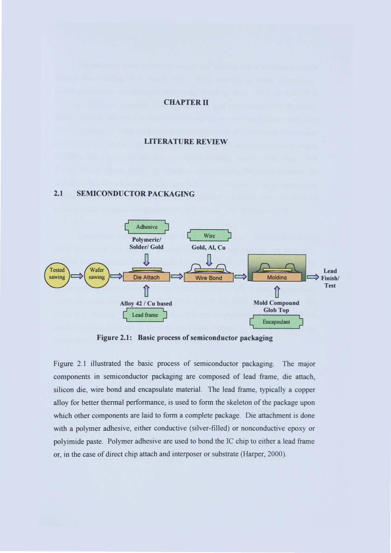
Figure 2.1: Basic process of semiconductor packaging
Figure 2.1 illustrated the basic process of semiconductor packaging. The major
components in semiconductor packaging are composed of lead frame, die attach,
silicon die, wire bond and encapsulate material. The lead frame, typically a copper
alloy for better thermal performance, is used to form the skeleton of the package upon
which other components are laid to form a complete package. Die attachment is done
with a polymer adhesive, either conductive (silver-filled) or nonconductive epoxy or
polyimide paste. Polymer adhesive are used to bond the Ie chip to either a lead frame
or, in the case of direct chip attach and interposer or substrate (Harper, 2000).
17
The electrical contacts between the die and bonding pad of substrate are made
through the bonding of a metal wire. Wire bonding is either thermosonic,
thermocompression or ultrasonic ball-wedge bonding using 0.001 to 0.00125-in
(0.025 to 0.032mm) diameter, 99.99 percent pure gold wire (pecht, 1991 & Harper,
2000). Copper wire has also been evaluated and can be used but requires much more
care. The choice is often made based on a combination of factors such as cost, size
and reliability. Thermocompression bonding is commonly used and requires both heat
(>300°C) and pressure to join the two metals together, usually by forming a ball
(pecht, 1991 & Harper, 2000). In ultrasonic wedge bonding, the heat is generated by
ultrasound and the substrate remains around room temperature. Finally, thermosonic
bonding uses a combination of ultrasound and pressure and better results are obtained
at intermediate substrate temperatures of 125°C (pecht, 1991 & Harper, 2000).
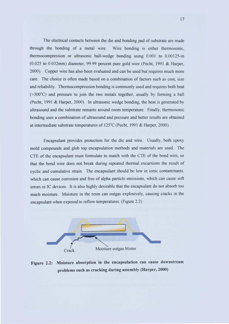
Encapsulant provides protection for the die and wire. Usually, both epoxy
mold compounds and glob top encapsulation methods and materials are used. The
CTE of the encapsulant must formulate to match with the CTE of the bond wire, so
that the bond wire does not break: during repeated thermal excursions the result of
cyclic and cumulative strain. The encapsulant should be low in ionic contaminants,
which can cause corrosion and free of alpha particle emissions, which can cause soft
errors in IC devices. It is also highly desirable that the encapsulant do not absorb too
much moisture. Moisture in the resin can outgas explosively, causing cracks in the
encapsulant when exposed to retlow temperatures. (Figure 2.2)
_.F Crack
Figure 2.2: Moisture absorption in the encapsulation can cause downstream
problems such as cracking during assembly (Harper, 2000)
18
2.2 THIN FILM TRANSISTOR TECHNOLOGIES
Flat-panel displays (FPDs) are becoming increasingly common in today's commercial
electronic devices and they are widespread use in many new products, such as ceUular
phones, personal digital assistants (PDAs), camcorders, and laptop personal computers
(PCs). FPDs in these devices are expected to be lightweight, portable, low-power and
high-resolution. Displays having these entire characteristic will enable a wide variety
of commercial applications in the future (Chung, 1995).
Active-matrix liquid-crystal displays (AMLCDs) are the leading flat-panel
display technology. These displays are present in laptops, often dubbed "active
matrix TFT," (active-matrix thin-film transistor), a display is composed of a grid (or
matrix) of pixels (picture elements). Thin-film transistors (TFTs) act as switches to
turn each pixel "on" (light) or "off' (dark). The TFTs are the active elements that
more responsive to change. For example, when you move your mouse across the
screen, a TFT display is fast enough to reflect the movement of the mouse cursor.
With a passive matrix display, the cursor temporarily disappears until the display can
"catch up" (Chung, 1995).
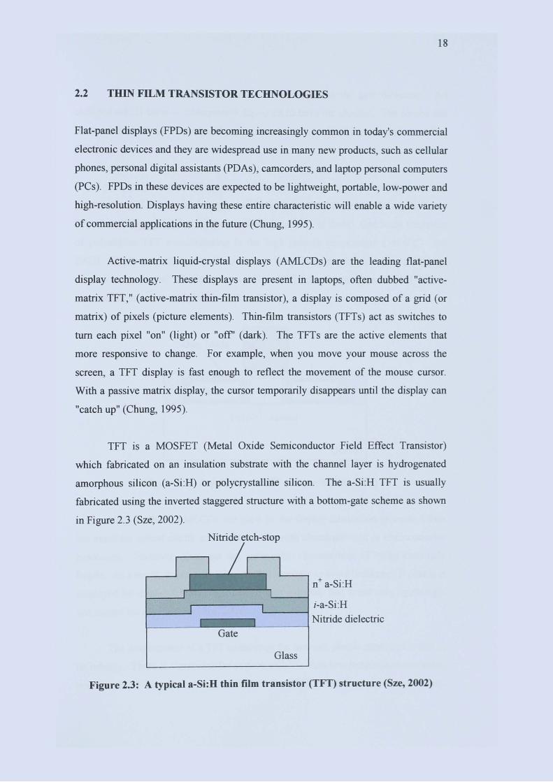
TFT is a MOSFET (Metal Oxide Semiconductor Field Effect Transistor)
which fabricated on an insulation substrate with the channel layer is hydrogenated
amorphous silicon (a-Si :H) or polycrystalline silicon. The a-Si :H TFT is usually
fabricated using the inverted staggered structure with a bottom-gate scheme as shown
in Figure 2.3 (Sze, 2002).
Nitride etch-stop
n+ a-Si :H
i-a-Si :H L-----i
L---~.~ •• ---~ Nitride dielectric Gate
Glass
Figure 2.3: A typical a-Si:H thin film transistor (TFT) structure (Sze, 2002)
19
Silicon nitride or silicon dioxide is often used as the gate dielectric. An
undoped a-Si:H layer is subsequently deposited to form the channel. The source and
drain of the TFT are formed with an in situ-doped n+ a-Si:H layer complying (Sze
2002).
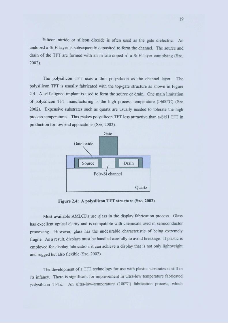
The polysilicon TFT uses a thin polysilicon as the channel layer. The
polysilicon TFT is usually fabricated with the top-gate structure as shown in Figure
2.4. A self-aligned implant is used to form the source or drain. One main limitation
of polysilicon TFT manufacturing is the high process temperature (>600°C) (Sze
2002). Expensive substrates such as quartz are usually needed to tolerate the high
process temperatures. This makes polysilicon TFT less attractive than a-Si:H TFT in
production for low-end applications (Sze, 2002).
Gate
Gate oxide
Poly-Si channel
Quartz
Figure 2.4: A polysilicon TFT structure (Sze, 2002)
Most available AMLCDs use glass in the display fabrication process. Glass
has excellent optical clarity and is compatible with chemicals used in semiconductor
processing. However, glass has the undesirable characteristic of being extremely
fragile . As a result, displays must be handled carefully to avoid breakage. If plastic is
employed for display fabrication, it can achieve a display that is not only lightweight
and rugged but also flexible (Sze, 2002).
The development of a TFT technology for use with plastic substrates is still in
its infancy. There is significant for improvement in ultra-low temperature fabricated
polysilicon TFTs. An ultra-low-temperature (lOO°C) fabrication process, which
20
would be compatible with flexible plastic substrates, is being developed by the TFT
technology group at DCB. The goal is to achieve polycrystalline-silicon TFTs with
current-driving capability far exceeding that of conventional amorphous-silicon TFTs
typically employed in high-performance active-matrix liquid-crystal displays today.
Techniques for formation of the poly-Si and gate-dielectric materials are being
investigated in order to determine the optimum processes for high-performance TFTs.
Various device and process architectures for attaining low leakage current are being
studied. The degradation of TFT performance under high-voltage bias stressing will
also be characterized. To enable device modeling and circuit design, a physically
based model for ultra-Iow-temperature-fabricated TFTs will be developed.
2.3 DIE ATTACHMENT TECHNIQUES
Different bonding techniques are used to provide electrical connections between the
chip pads and package. Die attachment performs several critical function. It must
provide a good thermal path between die and the package which usually attached to a
heat sink to remove the heat generated during operation (Ponchak). These can be
classified as follows.
2.3.1 Wire Bonding
Wire bonding is a method used to connect a fine wire between an on-chip pad and a
substrate pad. This substrate may simply be the ceramic base of a package or another
chip. The common materials used are gold and aluminum (pecht, 1991). The main
advantage of wire bonding technology is its low cost; but it cannot provide large I/O
counts and it needs large bond pads to make connections (Sze, 1988). The
connections have relatively poor electrical performance.
2.3.2 Tape-Automated Bonding
In tape-automated bonding (TAB) technology, a chip with its attached metal films is
placed on a multilayer polymer tape. The interconnections are patterned on a
21
multilayer polymer tape. The tape is positioned above the "bare die" so that the metal
tracks (on the polymer tape) correspond to the bonding sites on the die. TAB
technology provides several advantages over wire bonding technology. It requires a
smaller bonding pad, smaller on-chip bonding pitch and a decrease in the quantity of
gold used for bonding. It has better electrical performance, lower labor costs, higher
I/O counts and lighter weight, greater densities and the chip can be attached in a face
up or face-down configuration. TAB technology includes time and cost of designing
and fabricating the tape and the capital expense of the TAB bonding equipment. In
addition, each die must have its own tape patterned for its bonding configuration.
Thus, TAB technology has typically been limited to high-volume applications (Pecht,
1991).
2.3.3 Solder Bump Bonding
Solder bumps are small spheres of solder (solder balls) that are bonded to contact pads
of semiconductor devices. The length of the electrical connections between the chip
and the substrate can be minimized by placing solder bumps on the die, flipping the
die over, aligning the solder bumps with the contact pads on the substrate and re
flowing the solder balls in a furnace to establish the bonding between the die and the
substrate. This technology provides electrical connections with minute parasitic
inductances and capacitances. In addition, the contact pads are distributed over the
entire chip surface rather than being confined to the periphery. As a result, the silicon
area is used more efficiently, the maximum number of interconnects is increased and
signal interconnections are shortened. But this technique results in poor thermal
conduction, difficult inspection of the solder bumps and possible thermal expansion
mismatch between the semiconductor chips and the substrate (Harper, 2000).
2.4 DIE ATTACBJ\1ENT PROCESS
The process of mounting a semiconductor die or chip to a substrate or package is
known as die attach as shown in Figure 2.5 (Stockham, 2001 & Harper, 2000). The
die is attached mechanically to the substrate either by an organic adhesive, such as a
22
silver-filler epoxy or by a metal solders. This is a low-temperature process and care
must be taken not to stress the die through differences in the thermal expansions of the
material.
Automatic syringe dispensing, screen printing and stamping paste adhesives
are the popular production methods for attaching lCs and other chip devices. Control
of the epoxy flow is an important consideration in die attach. Excessive flow-out will
contaminate adjacent bonding sites and require additional cleaning steps (Stockham,
2001 & Harper, 2000).
The curing profile determines the properties of adhesive after cure. The best
cure profile is determined from the results of RGA testing, x-ray, die shear and/or
centrifuge testing, combined with the throughput demands of the production
environment. Once an epoxy is fully cured, it is shall not to exceed the cure
temperature for extended periods of time, because the epoxy will begin to break down
and lose strength (Stockham, 2001 & Harper, 2000).
Bond
Adhesive
I !~ace ~e
Placement Heat Cure
Figure 2.5: Die Attachment Process (Harper, 2000)
2.5 ELECTRICALLY CONDUCTIVE ADHESIVES
Electrically conductive adhesives (BCAs) are gaining great interest as potential solder
replacements in microelectronics assemblies. Basically, there are two types of ECAs,
isotropic conductive adhesive (ICA) and anisotropic conductive adhesive (ACA).
Although the concepts of these materials are different, both materials are composite
materials consisting of a polymer matrix containing conductive fillers. Typically,
lCAs contain conductive filler concentrations between 20 and 35 vol.% and the
adhesives are conductive in all directions. lCAs are primarily utilized in hybrid


![Factors tht affect recruitment[ppt]](https://img.pdfslide.us/doc/110x75/54541a88b1af9f84228b493f/factors-tht-affect-recruitmentppt.jpg)