Embed Size (px)
Citation preview

1
September 11-16, 2016 Hyatt Regency Orange County
Garden Grove (Anaheim), CA, USA
38thAnnual EOS/ESD Symposium
& Exhibits2016
EOS/
ESD ASSOCIATION, INC.
EOS/ESD SYMPOSIUM & EXHIB
ITS
September 11-16Garden Grove (Anaheim) CA.
Setting the Global Standards for Static Control! EOS/ESD Association, Inc. 7900 Turin Rd., Bldg. 3 Rome, NY 13440-2069, USA
PH +1-315-339-6937 • Email: [email protected] • www.esda.org
IEEECo-sponsored by IEEE, The Electron Devices Society, EMC Society, and Reliability Society.
R
The International Technical Forum on Electrical Overstress and Electrostatic Discharge
30 August 2016 8:04 AM

2
Dear Colleagues and fellow EOS/ESD enthusiasts,On behalf of the EOS/ESD Association, Inc. and the 2016 Symposium Steering Committee, I cordially welcome you to the 38th annual EOS/ESD Symposium, held at the Hyatt Regency Orange County in Garden Grove (Anaheim), California. Continuing its long tradition, the 2016 EOS/ESD Symposium will address the latest research on EOS and ESD in the rapidly changing world of electronics. As electronics continue to become commonplace in every aspect of our lives, including medical applications and the control of our homes and our cars, cost and reliability are of utmost importance. To accommodate these requirements and overcome challenges from the sensibility of advanced technologies, progress has to be made in the form of creative ESD design, innovative, comprehensive and predictive verification methods and on the side of the factory control standards and methods. The 2016 EOS/ESD Symposium addresses these matters and more through tutorials, workshops, technical sessions, invited talks and through the products and services presented in the industry exhibits.Our Industry Exhibits display a wide variety of ESD solutions from established products to leading-edge innovations. Representatives from many different companies welcome you in the exhibit hall to demonstrate their products and services, starting with the welcome reception on Monday evening and continuing until the exhibits close on Wednesday afternoon. The Exhibits offer a unique opportunity to find what you have been looking for or a chance to talk to the professionals with hands-on experience on static control methods, evaluation techniques, ESD testing hardware, and many other ESD solutions. Complimentary coffee will be available in the exhibit hall, so please stop by and visit the exhibitors. At the beginning of several technical sessions a short exhibitor showcase is highlighting some of the products and services you can expect to experience.A dedicated team of experts in all areas of EOS and ESD has been working diligently all year to prepare the tutorial program. Tutorials are offered on Sunday, Monday, and Thursday. ESDA tutorials have up-to-date and relevant information for anyone involved in the field of ESD, EOS, EMC and Latch-Up. Several new tutorials are available this year, including ESD Control Workstations, Basics of ESD Process Assessment and EDA Solutions for Latch-up. Also new are the Emerging Technology Seminars presented on Monday afternoon with two special courses on EMC design, PCB Design for Real-World EMC Control and Radiated Emissions, Understanding Product and Measurement Antenna Behavior presented by EMC Society lecturers Bruce Archambeault and Colin E. Brench, respectively. Many previously offered tutorials have been refreshed with updated material. This year may be a good time to circle back to bring yourself up to date with the latest in your field or learn something relevant in a new area.The heart of the symposium, the technical program, starts with the Awards Breakfast on Tuesday morning that includes an exciting keynote presentation by Professor Thomas Lee from Stanford University. His talk “Silicon is the new Steel: Building the World’s first Terascale Network” addresses the trends that are pushing us toward the terascale age, presenting us with both historic opportunities and historic challenges, ranging from design tools to hardening a trillion devices to ESD and other threats.The main technical program, which starts after the Awards Breakfast, includes 45 outstanding presentations of 44 peer reviewed and one invited paper, addressing latest innovations in the area of EOS and ESD. These will be presented Tuesday through Thursday in 13 sessions covering hot topics in the areas of factory and materials, advanced CMOS, high voltage and RF ESD challenges, real world EOS/ESD case studies, device physics and modeling, ESD EDA tools, system level ESD, and ESD testing. The papers are presented by experts working on leading edge research and development in these areas. The audience is invited to meet the authors to discuss the presented research work at the author’s corners following each technical session. This year’s technical program also features two Year-in-Review presentations. On Wednesday morning, Marty Johnson and Scott Ward will present how Latch-up and HBM standards continue to adapt to meet the needs of the industry and on Thursday morning, Michael Khazhinsky will present The Evolution of Verification Tools for ESD Protection Engineering.The seven symposium workshops taking place on Tuesday and Wednesday late afternoon offer an interactive forum for sharing experiences, exchanging knowledge, and jointly searching for and defining possible solutions. All workshops are centered on relevant and timely technical topics, each workshop allows participants the opportunity to learn about different perspectives from other colleagues in the field and allow the discussion of sometimes controversial topics in an informal environment. For the first time this year, a world café style workshop was added to discuss EOS Analysis and Diagnosis in a new interactive format that promises to be very productive.With so many exciting options and events, I am confident that the 2016 EOS/ESD Symposium will be a truly rewarding experience for everyone and will provide many opportunities to broaden your professional and personal horizons. I am looking forward to seeing you at the Hyatt Regency in Anaheim.Sincerely,
Melanie EthertonDr. Melanie EthertonNXP Semiconductors2016 EOS/ESD Symposium General Chair
Gen
eral
Cha
ir’s
Wel
com
e

3
Registration, Fees, Hours ..........................................4General Information ...................................................4Welcome Reception...................................................5 Annual Meeting and Awards Breakfast ......................5Professional and Technical Women’s Reception .......5Schedule .................................................................6-7Keynote .....................................................................8 Professional Certification .....................................9-10Tutorial Tracks ......................................................... 11Emerging Topics ......................................................12ESD Program Development and Assessment (ANSI/ESD S20.20 Seminar) ...................................12Tutorials ..............................................................13-22Technical Sessions .............................................23-30Workshops .........................................................31-32Exhibits ....................................................................33ESDA Officers, Board of Directors, and HQ Staff ....34Symposium Committees ..........................................34Technical Program Committee ................................34Hotel Reservations & Information ............................35Registration Form ...............................................36-37
www.esda.org/events/eosesd-symposia/

4
General Information Symposium ProceedingsEach paid registrant receives one electronic copy of the proceedings.
Tutorial NotesCustomized, full color tutorial notes will be provided to each tutorial registrant.
Hospitality SuitesTo maintain the objectives of the Symposium, the EOS/ESD Association, Inc. encourages all exhibitors and guest organizations to schedule their hospitality and other social events at times that do not conflict with the Symposium presentations and educational activities.
Age LimitsNo one under 18 years of age will be admitted to the exhibit hall.
Unauthorized SolicitationSolicitation of business on the premises during the EOS/ESD Symposium by manufacturers or others who are not participating as exhibitors is prohibited.
RecordingVideo and/or audio recording of Symposium events is prohibited without the prior written authorization of the EOS/ESD Association, Inc..
Gen
eral
Info
rmat
ion
Register Online! www.esda.org/events/eosesd-symposia/
On-Site Registration HoursRegistration will be open at the following times:
Sunday, September 11 7:30 a.m. - 5:00 p.m.Monday, September 12 7:30 a.m. - 5:00 p.m.Tuesday, September 13 7:30 a.m. - 5:00 p.m.Wednesday, September 14 7:30 a.m. - 5:00 p.m.Thursday, September 15 7:30 a.m. - 5:00 p.m.
Save by registering in advance! This will facilitate your registration upon your arrival at the Symposium. Early registration and member discounts* are valid only if received no later than July 21, 2016.
Symposium $800 (Includes technical sessions, workshops, and exhibits) Early Registration Fees valid until July 21, 2016EOS/ESD Association, Inc. Members* $600/Non-Members $700
Tutorials $710 (Sunday, Monday, OR Thursday (Full Day)) Early Registration Fees valid until July 21, 2016EOS/ESD Association, Inc. Members* $510/Non-Members $610
Bundled Fees $2,465 (Symposium plus Sunday, Monday, and Thursday full tutorial days) Early Registration Fees valid until July 21, 2016EOS/ESD Association, Inc. Members* $1,785/Non-Members $2,165 Emerging Topics $95(Attendance limited to first 50 registrants)These seminars are not included in the bundled fee.
ESD Program Development and Assessment (ANSI/ESD S20.20 Seminar) $1,710(Attendance limited to first 30 registrants)This seminar is not included in the bundled fee. Early Registration Fees valid until July 21, 2016EOS/ESD Association, Inc. Members* $1,510/Non-Members $1,610
*Membership discounts apply to those who participate as members all year long and are current at the opening of symposium registration. Memberships processed after this date will not apply. You will receive a complimentary 2017 membership with your Symposium registration which will allow you to enjoy the full benefits of membership in 2017.
Register 5 or more people from one company at the same time and save $100 per person. Please contact the EOS/ESD Association, Inc. prior to registering.
Student FeesThe EOS/ESD Symposium offers a fifty percent discount for full-time students. Proof of enrollment required. Student fees apply only to sym-posium or tutorial registration and do not apply to bundled fees, ANSI/ESD S20.20 seminar, or Emerging Topics.

5
Welcome ReceptionA welcome reception for all attendees will be held on Monday, September 12th, at 6:00 p.m. in the exhibit hall. Network with your colleagues, share your ESD work experiences with others, view the exhibits, or simply pass the time meeting new people and making new friends. The 2016 Steering Committee will greet you and answer any questions regarding the Symposium.
Annual Meeting and Awards Breakfast The annual meeting and awards breakfast for all registered attendees and exhibitors will be held Tuesday, September 13th, at 7:30 a.m. following breakfast, General Chair Melanie Etherton will officially open the Symposium. Vice General Chair Junjun Li will present the 2015 EOS/ESD Symposium paper awards. Technical Program Chair James Miller will cover highlights of the 2016 technical program. Association President Gianluca Boselli will present the Association’s annual report. Awards Chair, Charvaka Duvvury, will present the 2016 Association awards.
Professional and Technical Women’s ReceptionThe Professional and Technical Women’s Reception provides a friendly environment where women in the field of ESD can network and share work experiences. This year’s reception will be held on Monday, September 12th, from 5:00 to 6:00 p.m.

6
SUNDAY, SEPTEMBER 11, 2016Registration 7:30 a.m. - 5:00 p.m.S20.20 Seminar 8:00 a.m. - 5:00 p.m. FC340: ESD Program Development and Assessment (ANSI/ESD S20.20 Seminar) (PrM) (Day 1)Tutorials 8:00 a.m. - 5:00 p.m. FC100: ESD Basics for the Program Manager (PrM) 8:30 a.m. - 12:00 p.m. DD110: ESD from Basics to Advanced Protection Design (DD) 8:30 a.m. - 12:00 p.m. DD200: Charged Device Model Phenomena, Design, and Modeling (DD) 8:30 a.m. - 12:00 p.m. DD211: EOS/ESD Failure Models and Mechanisms (DD) 8:30 a.m. - 12:00 p.m. DD/FC122: Use of the Digital Sampling Oscilloscope for ESD Measurements 8:30 a.m. - 12:00 p.m. DD/FC230: System Level ESD/EMI: Principles, Design Troubleshooting, and Demonstrations 1:00 p.m. - 4:30 p.m. DD201: ESD Protection and I/O Design 1:00 p.m. - 4:30 p.m. DD204: ESD Design in HV Technologies REVISED 1:00p.m.-4:30p.m. DD240:ESDDeviceQualificationTesting REVISED 1:00 p.m. - 4:30 p.m. FC165: Novel Methods for Fixing ESD Issues in the Factory for Both Electronics & Explosive Products 1:00 p.m. - 4:30 p.m. FC215: Device Technology and Failure Analysis Overview (PrM) REVISEDStudy Session 5:00 p.m. - 6:00 p.m. Calculations and ESD Scenarios Review for ESD Program Manager Exam Preparation (STUDY SESSION)
MONDAY, SEPTEMBER 12, 2016Registration 7:30 a.m. - 5:00 p.m.S20.20 Seminar 8:00 a.m. - 5:00 p.m. FC340: ESD Program Development and Assessment (ANSI/ESD S20.20 Seminar) (PrM) (Day 2)Tutorials 8:30 a.m. - 4:30 p.m. FC101: How To’s of In-Plant ESD Auditing and Evaluation Measurements (PrM) 8:30 a.m. - 12:00 p.m. DD/FC130: System Level ESD/EMI: Testing to IEC & Other Standards (PrM, DD) NEW/REVISED 8:30 a.m. - 12:00 p.m. DD100: ESD Circuits 8:30 a.m. - 12:00 p.m. FC360: Electrical Overstress (EOS) in Manufacturing and Test 8:30 a.m. - 12:00 p.m. FC120: Air Ionization Issues and Answers for the Program Manager (PrM) 8:30 a.m. - 10:00 a.m. DD300: Circuit-Level Modeling and Simulation of On-Chip Protection (DD) 10:30 a.m. - 12:00 p.m. DD318: FinFET and Advanced CMOS Technology ESD TCAD Simulation 1:00 p.m. - 4:30 p.m. DD231: Integrated ESD Device and Board Level Design REVISED 1:00 p.m. - 4:30 p.m. DD311: Impact of Technology Scaling on Components High Current Phenomena and Implications for Robust ESD Design (DD) REVISED 1:00 p.m. - 4:30 p.m. DD302: Troubleshooting On-Chip ESD Failures (DD) 1:00 p.m. - 4:30 p.m. DD/FC155: ESD Control Workstations: Set-up, Practical Considerations and Measurements NEW 1:00 p.m. - 4:30 p.m. FC362: Using Different Air Ionization Technologies and Measuring Process Effects Emerging Topics 1:00 p.m. - 2:30 p.m. PCB Design for Real-World EMC Control NEW 3:00 p.m. - 4:30 p.m. Radiated Emissions, Understanding Product and Measurement Antenna Behavior NEWReception 5:00 p.m. - 6:00 p.m. Professional and Technical Women’s Reception Welcome Reception 6:00 p.m. - 9:00 p.m. Exhibits Open
TUESDAY, SEPTEMBER 13, 2016Registration 9:00 a.m. - 5:00 p.m.Awards Breakfast 7:30 a.m. - 9:45 a.m. Annual Meeting and Awards BreakfastKeynote 9:00 a.m. - 9:45 a.m. Silicon is the New Steel: Building the World’s First Terascale NetworkExhibits Open 9:30 a.m. - 5:30 p.m.Technical Sessions 10:10 a.m.-10:20 a.m. Exhibitor Showcase in Session 1A 10:20 a.m.-12:00 p.m. 1A: High Voltage I 1:10 p.m. - 1:20 p.m. Exhibitor Showcase in Sessions 2A and 2B 1:20 p.m. - 3:00 p.m. 2A: On Chip Physics I 1:20 p.m. - 2:35 p.m. 2B: Factory Control I 3:45 p.m. - 3:55 p.m. Exhibitor Showcase in Sessions 3A and 3B 3:55 p.m. - 5:10 p.m. 3A: Advanced CMOS I 3:55 p.m. - 5:10 p.m. 3B: System Level ESD IStudy Session 5:00 p.m. - 6:00 p.m. Calculations and ESD Scenarios Review for ESD Program Manager Exam Preparation (STUDY SESSION)
2016
Sym
posi
um S
ched
ule

7
TUESDAY, SEPTEMBER 13, 2016 continuedWorkshops A 5:30 p.m. - 7:00 p.m. A1. Should the Industry Council Address Adequate IEC 61000-4-2 Levels? A2. EOS Issues in Automotive Industry – What Information Needs to be Exchanged to Solve the Issue? A3.EDAESDVerificationToolsUtilizedinIndustryToday.Good,Bad,orJustPlainUgly? WEDNESDAY, SEPTEMBER 14, 2016Registration 7:30 a.m. - 5:00 p.m.Exhibits Open 7:30 a.m. - 1:10 p.m.Technical Sessions 8:00 a.m. - 8:40 a.m. Year in Review: 9:30 a.m. - 9:40 a.m. Exhibitor Showcase in Sessions 4A and 4B 9:40 a.m. - 10:55 a.m. 4A: Tester and Testing Methods 9:40 a.m. - 10:55 a.m. 4B: Factory Control II 1:10 p.m. - 1:20 p.m. Exhibitor Showcase in Sessions 5A and 5B 1:20 p.m. - 3:00 p.m. 5A: High Voltage II 1:20 p.m. - 3:00 p.m. 5B: EDA Tools 3:20 p.m. - 5:00 p.m. 6A: Advanced CMOS II 3:20 p.m. - 4:35 p.m. 6B: ESD Failure Case Studies IWorkshopsB 5:30p.m.-7:00p.m. B1.ComplianceVerification-TR53 B2.HighPinCountESDDeviceQualification B3. Correlation Between Component and System Level ESD Testing B4. EOS Analysis and Diagnosis - “Techniques and Methods for Dealing with EOS Induced Damage”
THURSDAY, SEPTEMBER 15, 2016Registration 7:30 a.m. - 5:00 p.m.Technical Sessions 8:00 a.m. - 8:40 a.m. Year in Review: 8:50 a.m. - 10:05 a.m. 7A: On Chip Physics II 10:25 a.m. - 11:40 a.m. 8A: System Level ESD II 11:40 a.m. - 11:45 a.m. Technical Session Closing 11:45 a.m. - 12:05 p.m. Author’s Corner Tutorials 8:30 a.m. - 4:30 p.m. FC390: Basics of ESD Process Assessment NEW 8:30 a.m. - 4:30 p.m. FC170: ANSI/ESD S20.20 – ESD Program Assessment for Internal Auditors and Supplier Quality Engineers 8:30 a.m. - 12:00 p.m. FC361: Class 0A Devices & Boards - ESD Controls and Auditing Measurements 8:30 a.m. - 10:00 a.m. DD117: TCAD Fundamentals 8:30 a.m. - 10:00 a.m. DD112: Latch-up Fundamentals (DD) 10:30 a.m. - 12:00 p.m. DD102: On-Chip ESD Protection in RF Technologies (DD) 10:30 a.m. - 12:00 p.m. DD213: ESD, EOS and Latch-up Failure Analysis for Designers 1:00 p.m. - 4:30 p.m. DD220: Transmission Line Pulse (TLP) Basics and Applications (DD) 1:00 p.m. - 4:30 p.m. FC115: Contamination & ESD Issues in Flat Panel Display Manufacturing Process 1:00 p.m. - 2:30 p.m. DD382: Electronic Design Automation (EDA) Solutions for Latch-up NEW 3:00 p.m. - 4:30 p.m. DD322: Advanced Latch-up Testing, Failure Analysis, and Prevention by Design Constraints and Tools
FRIDAY, SEPTEMBER 16, 2016 8:00a.m.-5:00p.m. DeviceDesignCertificationExam 8:00a.m.-5:00p.m. ProgramManagerCertificationExam

8
Key
note
Prof. Thomas Lee, Stanford University Thomas Lee received his degrees from MIT, and an hon-orary doctorate from the University of Waterloo. His 1989 doctoral thesis described the world’s first CMOS radio. He has been at Stanford University since 1994, hav-ing previously worked at Analog Devices, Rambus and other companies. He’s helped design PLLs for several microprocessors (notably AMD’s K6-K7-K8 and DEC’s StrongARM), and has founded or cofounded several companies, including the first 3D memory company, Ma-trix Semiconductor (acquired by Sandisk), and IoE com-panies ZeroG Wireless (acquired by Microchip) and Ayla Networks. He serves on the board of Xilinx, is an IEEE and Packard Foundation Fellow, has won “Best Paper” awards at CICC and ISSCC, and was awarded the 2011 Ho-Am Prize in Engineering. He is a past Director of DARPA’s Microsystems Technology Office, and owns between 100 and 200 oscilloscopes, thousands of vacu-um tubes, and kilograms of obsolete semiconductors. No one, including himself, quite knows why.
SILICON IS THE NEW STEEL: BUILDING THE WORLD’S FIRST TERASCALE NETWORKProf. Thomas Lee, Stanford UniversitySteel transformed civilization in the 20th century, shifting from high-tech material to commodity in the process. Silicon’s analogous shift from circuits to systems will similarly transform civilization in this century. This talk will argue that multiple convergent trends are pushing us toward the terascale age, presenting us with both historic opportunities and historic challenges. The latter extend from DC to the millimeter wave, and from design tools to hardening a trillion devices to ESD and other threats. Solving these problems will complete the transition of silicon from today’s ubiquity to tomorrow’s invisibility, the true mark of a successful technology.

9
EOS/ESD Association, Inc. Professional CertificationThe EOS/ESD Association, Inc. offers professional certification for ESD control program managers and device design technical specialists.
ESD Certified Professional-Program Manager The impact of the ANSI/ESD S20.20 ESD control program standard on the global industry has been extraordinary. As a result, the Association recognizes the need to offer a certification program for individuals that are involved in design-ing, implementing, managing, and auditing ESD control programs in their facilities. The program manager certification program serves that purpose. In addition, the needs of the technical community for certification of various technical specialists are apparent. Requirements for certification include attending required prerequisite tutorials and passing a final exam. All of the pre-requisite courses may not be available in the 2016 Symposium tutorial program. Details of the certification program are also available at the registration desk.The preferred tutorial sequence for the program manager curriculum is:
COURSE TITLE FACE TO FACE TUTORIAL ONLINE
1 FC100 ESD Basics for the Program Manager Symposium, Sunday, Sept. 11
2 FC101 How To’s of In-Plant ESD Auditing and Evaluation Measurements Symposium, Monday, Sept. 12
3 FC110 Cleanroom Considerations for the Program Manager Online Academy
4 FC120 Air Ionization Issues and Answers for the Program Manager Symposium, Monday, Sept. 12 Online Academy
5 FC200 Packaging Principles for the Pro-gram Manager Online Academy
6 FC210 ESD Standards Overview for the Program Manager Online Academy
7 DD/FC130 System Level ESD/EMI: Test-ing to IEC and Other Standards Symposium, Monday, Sept. 12 Online Academy
8 FC215 Device Technology and Failure Analysis Overview Symposium, Sunday, Sept. 11 Online Academy
9 FC380 Electrostatic Calculations for the Program Manager and the ESD Engineer Online Academy
10 FC340 ESD Program Development & As-sessment (ANSI/ESD S20.20 Seminar) Symposium, Sunday & Monday, Sept. 11 & 12
ESDA Certification ExamThe certified professional program manager exam will be held on Friday, September 16th. To take the exam, applicants must have a registration form on file with EOS/ESD Association, Inc. headquarters complete with a $50 filing fee prior to the Symposium. Applicants must also have completed all required courses and had their eligibility verified by EOS/ESD Association, Inc. An exam fee of $60 is applicable (in addition to the filing fee). Please note: each of the test sec-tions include essay questions that require a good understanding of English. Up to 50% of the grade in each section may involve essay and short written answers. The exam is open book. You may bring any reference materials, including, but not limited to, books, standards, and tutorial notes. You may also bring a calculator and computer. No cell phones, internet connections, or sharing of reference materials is allowed.
Offer to Certified iNARTE Engineers: The EOS/ESD Association, Inc. is offering iNARTE certified ESD engineers the opportunity to take the program manager certification exam without taking all required courses. Simply show a current iNARTE card, pay the exam fee, and take the exam. Please note that the program manager exam covers additional material not covered in the iNARTE exam and may be more difficult.
iNARTE Certification ExamThe iNARTE certification exams for ESD engineers and ESD technicians will be offered on Friday, September 16th. Appli-cants must complete an application form and submit the application fee to iNARTE prior to the exam. For more information visit www.inarte.org/.
Certifi
catio
n

10
Certifi
catio
nESD Certified Professional-Device DesignESD device design certification was developed for individuals that are involved in designing, testing, characterizing, and implementing improved ESD protection designs. Device design certification demonstrates knowledge, experience, and competency in the area of ESD design and test for device protection.Requirements for certification include attending required prerequisite tutorials and passing a final exam. All of the pre-requisite courses may not be available in the 2016 Symposium tutorial program. Details of the certification program are also available at the registration desk.The preferred tutorial sequence for the device design curriculum is:
COURSE TITLE FACE TO FACE TUTORIAL ONLINE
1 DD110:Overview of ESD and Related Effects for Device/Design Symposium, Sunday, Sept. 11
2DD301: SPICE-Based ESD Protection De-sign Utilizing Diodes and Active MOSFET Rail Clamp Circuits
3 DD211: EOS/ESD Failure Models and Mech-anisms Symposium, Sunday, Sept. 11
4 DD102: On-Chip ESD Protection in RF Tech-nologies Symposium, Thursday, Sept. 15 Online Academy
5 DD200: Charged Device Model Phenomena, Design, and Modeling Symposium, Sunday, Sept. 11 Online Academy
6 DD112: Latch-up Fundamentals Symposium, Thursday, Sept. 15 Online Academy
7 DD300: Circuit-Level Modeling and Simula-tion of On-Chip Protection Symposium, Monday, Sept. 12
8 DD302: Troubleshooting On-Chip ESD Fail-ures Symposium, Monday, Sept. 12
9 DD120: Device Testing--IC Component Level: HBM, CDM, MM, and TLP
10DD311: Impact of Technology Scaling on ESD High Current Phenomena and Implications for Robust ESD Design
Symposium, Monday, Sept. 12
11 DD220: Transmission Line Pulse (TLP) Ba-sics and Applications Symposium, Thursday, Sept. 15
12 DD/FC130: System Level ESD/EMI: Testing to IEC and other Standards Symposium, Monday, Sept. 12 Online Academy
ESDA Certification ExamsThe certified professional device design exam will be held on Friday, September 16th. To take the exam, applicants must have a registration form on file with EOS/ESD Association, Inc. headquarters complete with a $50 filing fee prior to the Symposium. Applicants must also have completed all required courses and had their eligibility verified by the EOS/ESD Association, Inc. An exam fee of $60 is applicable (in addition to the filing fee). Please note: each of the test sections include essay questions that require a good understanding of English. Up to 50% of the grade in each section may involve essay and short written answers. The exam is open book. You may bring any reference materials, including, but not limited to, books, standards, and tutorial notes. You may also bring a calculator and computer. No cell phones, internet connections, or sharing of reference materials is allowed.

11
Device Design Certification Courses
Program Manager Certification Courses
Quarter Day Class8:30‐10:00
Quarter Day Class 10:30‐12:00
Quarter Day Class1:00‐2:30
Quarter Day Class 3:00‐4:30
Day TrackSunday
System Level ESD
Monday
DD300: Circuit‐Level Modeling and Simulation of On‐Chip Protection (DD)
DD318: FinFET and Advanced CMOS Technology ESD TCAD Simulation
ESD for IC Design
System Level ESD
Thursday
DD117: TCAD Fundamentals
DD102: On‐Chip ESD Protection in RF Technologies (DD)
DD382 ‐ Electronic Design Automation
(EDA) Solutions for Latch‐up NEW
DD322: Advanced Latch‐up Testing,
Failure Analysis and Prevention by Design Constraints and Tools
DD112: Latch‐up Fundamentals (DD)
DD213: ESD, EOS, and Latch‐up Failure
Analysis for Designers
DD220: Transmission Line Pulse (TLP) Basics and Applications (DD)
FC115: Contamination & ESD Issues in Flat Panel Display Manufacturing Process
ESD Technology
Factory Control & Testing
ESD Technology
ESD Technology
ESD for IC Design
FC390 ‐ Basics of ESD Process Assessment NEW
FC361: Class 0A Devices & Boards ‐ ESD Controls and Auditing Measurements
FC170: ANSI/ESD S20.20 – ESD Program Assessment for Internal Auditors and Supplier Quality Engineers
DD302: Troubleshooting On‐Chip ESD Failures (DD)
DD/FC155 ‐ ESD Control Workstations: Set‐up, Practical Considerations and Measurements
NEW
FC362: Using Different Air Ionization Technologies and Measuring Process Effects
DD/FC130: System Level ESD/EMI: Testing to IEC & Other Standards (PrM, DD, iNARTE)
NEW/REVISED
DD100: ESD Circuits
FC360: Electrical Overstress (EOS) in Manufacturing and Test
DD231: Integrated ESD Device and Board Level Design REVISED
DD311: Impact of Technology Scaling on Components High Current Phenomena and Implications for Robust ESD Design (DD)
DD240: ESD Device Qualification Testing REVISED
FC165: Novel Methods for Fixing ESD Issues in the Factory for Both Electronics & Explosive
Products FC215: Device Technology and Failure Analysis
Overview (PrM)
DD201: ESD Protection and I/O Design
DD204: ESD Design in HV Technologies
Factory Control & Testing
Factory Control & Testing
FC340: ESD Program Development and Assessment (ANSI/ESD S20.20 Seminar) (PrM)FC101: How To’s of In‐Plant ESD Auditing and Evaluation Measurements (PrM)
DD110: ESD from Basics to Advanced Protection Design (DD)
FC100: ESD Basics for the Program Manager (PrM)
FC120: Air Ionization Issues and Answers for the Program Manager (PrM)
DD200: Charged Device Model Phenomena, Design, and Modeling (DD)
DD211: EOS/ESD Failure Models and Mechanisms (DD)
DD/FC122: Use of the Digital Sampling Oscilloscope for ESD Measurements
DD/FC230: System Level ESD/EMI: Principles, Design Troubleshooting, and Demonstrations
Seminar/FC100 8:00‐5:00Full Day Class 8:30‐4:30
Half Day Class 8:30‐12:00 Half Day Class 1:00‐4:30
FC340: ESD Program Development and Assessment (ANSI/ESD S20.20 Seminar) (PrM)

12
EMERGING TOPICSMONDAY, SEPTEMBER 12PCB Design for Real-World EMC Control 1:00 p.m. - 2:30 p.m.Bruce Archambeault
Multi-layer PCBs typically contain a large number of different high speed signals. Successful routing of all these signals often require some of the standard EMC “rules” to be violated. However, not all of these EMC rules are equal, that is, some are more important than others. Understanding where the current flows is the first step to understanding which EMC design rules are the most important, and should receive the most effort and attention.
Dr. Bruce Archambeault is an IEEE Fellow, an IBM Distinguished Engineer Emeritus and an Adjunct Professor at Missouri University of Science and Technology. He received his B.S.E.E degree from the University of New Hampshire in 1977 and his M.S.E.E degree from Northeastern University in 1981. He received his Ph. D. from the University of New Hampshire in 1997.
His doctoral research was in the area of computational electromagnetics applied to real-world EMC problems. He has taught numerous seminars on EMC and Signal Integrity across the USA and the world, including the past 14 years at Oxford University.Dr. Archambeault has authored or co-authored a number of papers in computational electromagnetics, mostly applied to real-world EMC applications. He is a member of the Board of Directors for the IEEE EMC Society and a past Board of Directors member for the Applied Computational Electromagnetics Society (ACES). He currently serves as the Vice president for Conferences of the EMC Society. He has served as a past IEEE/EMCS Distinguished Lecturer , EMCS TAC Chair and Associate Editor for the IEEE Transactions on Electromagnetic Compatibility. He is the author of the book “PCB Design for Real-World EMI Control” and the lead author of the book titled “EMI/EMC Computational Modeling Handbook”.
Radiated Emissions, Understanding Product and Measurement Antenna Behavior3:00 p.m. - 4:30 p.m Colin E. Brench
Antenna behavior is complex in an environment that does not approach that of free space, and is particularly so if the antenna is incidental to a device or system. There are numerous, unintended antennas that are present in every electronic device. With the high data rates in use today, even small structures can be effective, unwanted antennas. The impact of how a device is mounted into a chassis or how a chassis is mounted into a rack can be unexpected. Every conductor with a radio frequency current on it is an antenna to some degree, and understanding how these unintended antennas are created and driven is a powerful tool in controlling radiated emissions. This presentation will first explore the behavior of both measurement antennas and unintended antennas. Secondly, various sized systems will be discussed, from the very small devices up though full sized racks of systems. Finally, animations of field propagation will be used to help visualize how the RF energy travels and is radiated. Important details such as the addition of a ferrite core filter on a cable and cable shield bonding will also be shown.
Colin Brench received his B.Sc. (Honours) in Electronic Engineering at The City University, London, in 1975. He has been particularly active in the areas of antenna and shielding behavior and EMC since the early 1970’s. In his current position at Amphenol TCS in Nashua, NH, Colin is responsible for the EMC aspects of high data rate (10 to 56 Gb/s) interconnect schemes. His previous position was at Southwest Research Institute (SwRI) in
San Antonio where he was a staff engineer in the Electromagnetic Compatibility Research group. His responsibilities at SwRI included developing new EMC technologies and providing consulting and training. Previous to that, he worked for 21 years at Hewlett-Packard (formerly Compaq Computer Corporation, formerly Digital Equipment Corporation) where he was involved in a wide range of server, workstation, and networking products.Mr. Brench has presented numerous EMC training classes that embrace a broad range of topics including microprocessor packaging, printed circuit module issues, system design, and shielding. He is a co-author of the book, EMI/EMC Computational Modeling Handbook (Springer Science & Business Media, 2nd Edition 2001), and has authored over 20 technical papers and articles. In addition, he holds 12 patents for various methods of EMI control. Mr. Brench was appointed a Distinguished Lecturer for the IEEE EMC Society for 2001 and 2002. In 2002 he was awarded the Certificate of Technical Achievement by the IEEE EMC Society for his contributions to the development of EMC modeling directed to understanding EMI shielding and antenna behavior. Mr. Brench is a Senior Member of the IEEE, a member of the EMC Society since 1980, and has been an iNARTE certified EMC Engineer since 1990. He is also active in IEEE EMC-S standards, IEEE EMC-S Technical Committee 9 (TC-9), and ANSI ASC63. He is currently serving as the VP for technical Services on the IEEE EMC-S Board of Directors.
Emer
ging
Top
ics

13
EMERGING TOPICSSUNDAY AND MONDAY, SEPTEMBER 11-12FC340: ESD Program Development and Assessment (ANSI/ESD S20.20 Seminar)8:00 a.m. - 5:00 p.m. Ron Gibson, Advanced Static Control Consulting; John T. Kinnear, IBM Corporation
ANSI/ESD S20.20 SEMINAR T
Certification: PrMThis seminar provides instruction on designing and implementing an ESD control program based on ANSI/ESD S20.20. The course provides participants with the tools and techniques to prepare for an ESD facility audit. This two-day course is an ESDA certification requirement for in-plant auditors and program managers who are working toward professional ESD certification.
The following topics are covered in this course:• Overview of ANSI/ESD S20.20• How to approach an assessment• Administrative elements• ESD program assessment• ESD program techniques for different applications• Technical elements• Overview of the assessment process• The audit checklist and follow-up questions
It is recommended that the ESD Program Development and Assessment Seminar be taken after the Certification candidate has taken most of the other program manager related tutorials.
Customized, full color tutorial notes will be provided to each tutorial registrant
AN
SI/E
SD S
20.2
0 Se
min
ar
14
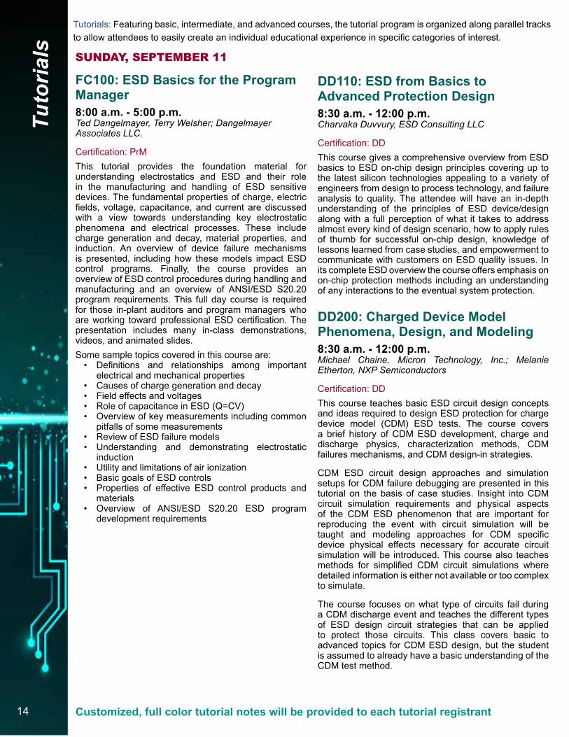
SUNDAY, SEPTEMBER 11
FC100: ESD Basics for the Program Manager 8:00 a.m. - 5:00 p.m.Ted Dangelmayer, Terry Welsher; Dangelmayer Associates LLC.
Certification: PrMThis tutorial provides the foundation material for understanding electrostatics and ESD and their role in the manufacturing and handling of ESD sensitive devices. The fundamental properties of charge, electric fields, voltage, capacitance, and current are discussed with a view towards understanding key electrostatic phenomena and electrical processes. These include charge generation and decay, material properties, and induction. An overview of device failure mechanisms is presented, including how these models impact ESD control programs. Finally, the course provides an overview of ESD control procedures during handling and manufacturing and an overview of ANSI/ESD S20.20 program requirements. This full day course is required for those in-plant auditors and program managers who are working toward professional ESD certification. The presentation includes many in-class demonstrations, videos, and animated slides.Some sample topics covered in this course are:
• Definitions and relationships among important electrical and mechanical properties
• Causes of charge generation and decay • Field effects and voltages • Role of capacitance in ESD (Q=CV) • Overview of key measurements including common
pitfalls of some measurements • Review of ESD failure models • Understanding and demonstrating electrostatic
induction • Utility and limitations of air ionization • Basic goals of ESD controls • Properties of effective ESD control products and
materials • Overview of ANSI/ESD S20.20 ESD program
development requirements
DD110: ESD from Basics to Advanced Protection Design 8:30 a.m. - 12:00 p.m. Charvaka Duvvury, ESD Consulting LLC
Certification: DDThis course gives a comprehensive overview from ESD basics to ESD on-chip design principles covering up to the latest silicon technologies appealing to a variety of engineers from design to process technology, and failure analysis to quality. The attendee will have an in-depth understanding of the principles of ESD device/design along with a full perception of what it takes to address almost every kind of design scenario, how to apply rules of thumb for successful on-chip design, knowledge of lessons learned from case studies, and empowerment to communicate with customers on ESD quality issues. In its complete ESD overview the course offers emphasis on on-chip protection methods including an understanding of any interactions to the eventual system protection.
DD200: Charged Device Model Phenomena, Design, and Modeling8:30 a.m. - 12:00 p.m.Michael Chaine, Micron Technology, Inc.; Melanie Etherton, NXP Semiconductors
Certification: DDThis course teaches basic ESD circuit design concepts and ideas required to design ESD protection for charge device model (CDM) ESD tests. The course covers a brief history of CDM ESD development, charge and discharge physics, characterization methods, CDM failures mechanisms, and CDM design-in strategies.
CDM ESD circuit design approaches and simulation setups for CDM failure debugging are presented in this tutorial on the basis of case studies. Insight into CDM circuit simulation requirements and physical aspects of the CDM ESD phenomenon that are important for reproducing the event with circuit simulation will be taught and modeling approaches for CDM specific device physical effects necessary for accurate circuit simulation will be introduced. This course also teaches methods for simplified CDM circuit simulations where detailed information is either not available or too complex to simulate.
The course focuses on what type of circuits fail during a CDM discharge event and teaches the different types of ESD design circuit strategies that can be applied to protect those circuits. This class covers basic to advanced topics for CDM ESD design, but the student is assumed to already have a basic understanding of the CDM test method.
Tuto
rials
Customized, full color tutorial notes will be provided to each tutorial registrant
Tutorials: Featuring basic, intermediate, and advanced courses, the tutorial program is organized along parallel tracks to allow attendees to easily create an individual educational experience in specific categories of interest.

15
DD211: EOS/ESD Failure Models and Mechanisms8:30 a.m. - 12:00 p.m.Steven H. Voldman, Dr. Steven H. Voldman, LLC
Certification: DDESD and EOS failures continue to impact semiconductor components and systems as technologies scale from micro- to nano-electronics. This tutorial studies electrical overstress, ESD, and latch-up from a failure analysis and case-study approach. It provides insight into the physics of failure, followed by investigation of failure mechanisms in specific technologies, circuits, and systems. The tutorial covers both the failure mechanism and the practical solutions to fix the problem from either a technology or circuit methodology.
The failure of each key element of a technology from passives, active elements to the circuit, sub-system to package, highlighted by case studies of the elements, and circuits and system-on-chip (SOC) in today’s products.
DD/FC122: Use of the Digital Sampling Oscilloscope for ESD Measurements8:30 a.m. - 12:00 p.m.Larry B. Levit, LBL Scientific
The digital sampling oscilloscope (DSO) finds application in measuring waveforms that occur infrequently or only once. Its sophisticated calculation and display capabilities give it utility for factory ESD, as well as, its role in monitoring ESD immunity waveforms for both component and system level ESD. Understanding instrument performance issues is important for proper use. DSO bandwidth and the sampling rate are often used interchangeably, although they serve completely different purposes. The bandwidth, sampling rate and memory depth of the instrument must be specified for the intended application. DSOs also have display modes which can hide under sampling artifacts and lead to incorrect conclusions. Selecting the appropriate display algorithm is important for both cosmetic purposes and to achieve correct results from the instrument. Also important for the proper use of any oscilloscope are selection of the input impedance and the setup of the trigger. For a DSO, the pretrigger value must also be set. In some cases equivalent time sampling can be used but in most ESD measurements, single shot acquisition is required. Finally, for ESD applications on the factory floor, there are a variety of probes that are used. These include wide bandwidth current probes, clamp on current probes, single ended and differential voltage probes, as well as, high frequency antennas.
DD/FC230: System Level ESD/EMI: Principles, Design Troubleshooting, and Demonstrations8:30 a.m. - 12:00 p.m.Douglas Smith, D.C. Smith Consultants
This system level ESD tutorial will cover several facets of ESD as applied to electronic systems. Many of the principles and troubleshooting techniques will be demonstrated on real circuits for the students, with several new experiments added since previous years. “War” stories will also be used to illustrate points. The emphasis will be on making the experience both entertaining and informative for the students using an intuitive approach without heavy mathematics. Topics covered will include 1) Characteristics of ESD events; 2) ESD principles as applied to electronic systems; 3) Design troubleshooting techniques; 4) Unusual forms of ESD that have been the cause of field failures including internal chair discharges; 5) High-frequency measurement techniques; and 6) System design principles. It is recommended that those attending this tutorial section have at least one year of a college level electronics circuits course. Knowledge of common circuit analysis techniques will be assumed.
DD201: ESD Protection and I/O Design
1:00 p.m. - 4:30 p.m. Michael Stockinger, NXP Semiconductors
This tutorial is intended to provide the attendees with the tools to take a device and circuit level understanding of ESD protection methods and implement them effectively in I/O designs for CMOS bulk technologies. Beginning with a review of common ESD protection strategies, this course will focus more directly on how to build ESD-robust I/O cells and how to integrate them on a full chip. The tutorial will cover various types of I/O pads including analog, RF and digital pads. Different types of ESD protection strategies and their usage in I/O pad cells will be described, for example rail clamp, self-contained, and SCR based protection schemes. This course will also discuss the decisions and challenges which ESD and I/O designers typically face when designing I/O pads. More complex ESD solutions will also be described such as stacked rail clamps, ghost rails, and protecting signals that can swing below ground or above the supply. Finally, this tutorial will touch on various supply schemes including multiple power domains and isolated grounding schemes. It will end with discussing pad ring construction aspects for both wire-bond and flip-chip packages.
Customized, full color tutorial notes will be provided to each tutorial registrant
SUNDAY, SEPTEMBER 11

16
REVISED DD204: ESD Design in HV Technologies
1:00 p.m. - 4:30 p.m. Lorenzo Cerati, STMicroelectronics; Yiqun Cao, Infineon Technologies
This seminar gives an introduction to ESD design in high voltage technologies for integrated circuits with pin voltages from 12V upwards. After a short introduction of typical applications and requirements, an overview of different technologies and the typical device portfolios in these technologies will be given. Different ESD protection concepts are introduced, analyzing advantages and disadvantages of the various possible approaches to implement ESD networks (diodes, snapback devices, active clamps…). Finally, HV-technology and design related challenges regarding ESD protection are discussed, with a special focus on the formation on parasitic bipolar devices and their impact on the circuit’s ESD performance. The attendee will gain a good basic knowledge of the main characteristics of HV technologies, the different ESD protection concepts and ESD protection challenges that are specific for HV technologies. This will be a help for understanding and further development of HV ESD protection. An extensive literature list is provided for further study of various subjects regarding HV ESD.
REVISED DD240: ESD Device Qualification Testing 1:00 p.m. - 4:30 p.m.Brett Carn, Wolfgang Stadler, Intel Corporation
This tutorial addresses the details of both Human Body Model (HBM) and Charged Device Model (CDM) qualification testing. This course will help in interpretation of the HBM joint standard JEDEC/ANSI/ESD JS-001-2014 including the following details: Waveform verification, understanding of Table 2A (minimum required set of pin combinations) and Table 2B (legacy pin combinations), pin categorization and pin grouping, I/O pin sampling, stress plans details including efficient testing (reduction in pin count) and some debugging options. In addition, this course will discuss CDM testing details regarding waveform verification, stress plans, peak current (Ipeak) variability and how does it affect the testing results, and debugging options as well as an overview on the new CDM joint standard JEDEC/ANSI/ESD JS-002-2014.
FC165: Novel Methods for Fixing ESD Issues in the Factory for Both Electronics & Explosive Products
1:00 p.m. - 4:30 p.m. Jay Skolnik, Skolnik Technical Training
This class will be a 3-hour tutorial on ESD control for explosives and other energetic materials, introducing the students to the differences of ESD damage of electronics versus energetics. It will discuss the various energy levels and types of discharges which can cause catastrophic or latent failures. Enlightening demonstrations and case histories will be included to illustrate practical, real-life situations of past ESD-induced failures of energetic components and methods to prevent them, as well as explanations of the use of ESD mitigation in the work environment. Upon tutorial completion, the students should be able to understand ESD and the prevention of ESD failures be applying the proper mitigation & control techniques, as well as safely work with explosive applications while ensuring human safety, preventing catastrophic health hazards, injuries, and severe damages.
REVISED FC215: Device Technology and Failure Analysis Overview
1:00 p.m. - 4:30 p.m. Jim Vinson, Intersil Corporation
Certification: PrMThis tutorial is designed to give an overview of ESD protection technology and design, as well as an overview of the debug techniques used when a circuit fails to meet ESD performance requirements. The three major areas addressed are 1) a general overview of ESD, 2) circuit protection techniques, and 3) failure analysis. Failure analysis is the key to identifying and correcting weaknesses in ESD designs. The tutorial is NOT intended to turn the student into an ESD device or circuit designer nor a failure analyst. Rather, it is meant for program managers and other support personnel who are involved in the product development process to gain a better understanding of the language and challenges encountered supporting ESD robustness in new designs. After completing this tutorial, the student will be exposed to the key specifications governing ESD robustness and the common device architectures used to provide that robustness. The tutorial will include real world examples of protection designs and electrical characterization of those designs, as well as go through the tools and techniques used to debug a design.
Tuto
rials
Customized, full color tutorial notes will be provided to each tutorial registrant
SUNDAY, SEPTEMBER 11

17
MONDAY, SEPTEMBER 12
FC101: How To’s of In-Plant ESD Auditing and Evaluation Measurements8:30 a.m. - 4:30 p.m. Stephen Halperin, Stephen Halperin & Associates, Ltd.
Certification: PrM This program reviews the evaluation and periodic verification (audit) measurement procedures for the technical requirements specified in the ANSI/ESD S20.20 ESD program development standard. Detailed explanation of instruments, fixtures, and accessories function and usage are provided. Then, the details of “How to” measure are explained and demonstrated. Measurements include those listed in Table 1: Grounding/Equipotential Bonding Requirements; Table 2: Personnel Grounding Requirements; and Table 3: EPA/ESD Control Items. These recommended measurement procedures confirm the proper operation and use of ESD control products and materials selected as part of a facility’s S20.20 ESD control program. Some sample topics covered in this course are:
• ANSI/ESD S20.20 Technical Control Requirements• Program Manager’s Approach to Instrumentation and
Applications• Testing Ground Circuits and Assessing Connections• Essential Resistance Measurement Procedures and
Concerns• Electrostatic Field and Voltage Measurements• Personnel Grounding Considerations vs. ESD Control
Points• Product Installation Baseline Measurements• Evaluation, Acceptance, and Audit Procedures for:
Ground Systems, Floors, Worksurfaces, Equipment, Personnel Grounding, Garments, Materials, Production Aids, Packaging, and Ionization Devices
• Electrostatic Analysis Measurements including Worksurface Suppression, Footwear/Flooring, and Ionization Decay
NEW/REVISED DD/FC130: System Level ESD/EMI: Testing to IEC & Other Standards
8:30 a.m. - 12:00 p.m.Jeff Dunnihoo, Pragma Design, Inc.
Certification: PrM, DDThis tutorial is intended to help those tasked with testing products system level ESD standards by providing first an overview of how real-world system ESD events are simulated in different standards and testers in general, and then provide detailed information on IEC 61000-4-2, the most widely used standard. This introduction will highlight the similarities and differences between IEC, ANSI, Telcordia, and some automotive ESD standards. We will answer common questions regarding test setups, test points, and procedures, and address key issues, including: 1) Differences between “verification” and “calibration” and when is each required, 2) Test equipment requirements, the test environment, ground connections, return paths and ground plane effects. 3) Testing procedures with demonstration on actual products, how the tester and procedure affects test results, and problems with test result variations due to simulator influences. 4) Definitions of testing failure criteria for the product. 4) What points need to be tested and why, guidance on determining “operator accessible” points and ports, exempted points and ports, and what to do around connectors and connector pins. 5) ANSI and other ESD standards, the drive toward harmonization with IEC, the scope of different standards and why they are unlikely to converge. This system level ESD tutorial will cover different perspectives on ESD as applied to electronic systems from the user’s, the designer’s and even the designer’s competitor’s points of view.
DD100: ESD Circuits
8:30 a.m. - 12:00 p.m.Gene Worley, Qualcomm, Inc.
This tutorial will focus on a number of clamp approaches including BigFETs or RC clamps, snap-back NFETs, diodes, SCRs including HV SCRs, low capacitance clamps methods including those for MOSFET based LNAs and RF transceiver switches, and cross domain clamping. Spice simulations and simple models where applicable will be used to design and analyze circuit performance. Models include HBM, CDM, and IEC sources, gate pull requirements for dynamically lowering snap-back thresholds, and diodes. Gate pull for snap-back NFETs will include cascade and stacked NFETs. The need for NQS MOSFET models will be discussed with respect to CDM simulations. Operational characteristics of diodes will be examined including simple models and turn on delay. Diode types to be examined include STI, gated, and gated with LDD block. Protecting RF transceiver switches will be studied and will include spice simulations and design of low capacitance snap-back NFETs. Cross domain analysis will feature SPICE-based gate oxide rupture models and design requirement for secondary clamps including secondary clamps for LNAs.
18
FC360: Electrical Overstress (EOS) in Manufacturing and Test
8:30 a.m. - 12:00 p.m.Terry Welsher, Dangelmayer Associates LLC
Electrical overstress (EOS) is a major cause of device failure in manufacturing and in the field. Despite this, there is relatively little information on the sources of EOS and on prevention practices, particularly for the factory. In this tutorial, the fundamentals of device overstress are reviewed. Relationships among device EOS stressing models, such as the Wunsch-Bell curve, are discussed. The causes of EOS and EOS-like events in manufacturing are described and categorized by source and by stress-type. The difficulties in distinguishing between power-induced EOS and high current ESD events such as charged-board events (CBE) and cable discharge events (CDE) are discussed. Case histories, including failure analysis and root cause determination, are presented and the few relevant industry specifications are reviewed.
FC120: Air Ionization Issues and Answers for the Program Manager 8:30 a.m. - 12:00 p.m. Arnold Steinman, Electronics Workshop, Dangelmayer Associates LLC
Certification: PrM The primary method of static charge control is direct connection to ground for conductors, static dissipative materials, and personnel. Air ionization is also part of a static control program to deal with the problems of isolated conductors and insulating materials. This seminar is a basic course on ionizers, providing an introduction to their use, as well as application information. It examines common problems caused by static charge and the need for ionizers in a static control program. Types of ionizers, their use environments, and performance test methods using the Ionization Standard will be demonstrated. Installation, safety, maintenance, and contamination issues will be presented. Finally, case histories will be analyzed illustrating the use of ionizers in a variety of work environments.
DD300: Circuit-Level Modeling and Simulation of On-Chip Protection 8:30 a.m. - 10:00 a.m.Elyse Rosenbaum, University of Illinois at Urbana-Champaign
Certification: DDThis tutorial addresses modeling and simulation of protection circuit elements and networks under ESD conditions. The high-current characteristics and transient responses of devices typically used in ESD protection circuits will be presented. The objective is to ascertain what behaviors have to be captured in models intended for circuit-level simulation of ESD. Specific examples of model implementations will be provided. Parameter extraction and model scalability will be addressed. Thermal modeling will be discussed, as will be the issue of modeling the off-state behavior of ESD protection devices. This tutorial assumes some familiarity with device physics. It is directed toward persons with an interest in the transistor-level physics of ESD in on-chip protection circuits and an interest in computer-aided design.
DD318: FinFET and Advanced CMOS Technology ESD TCAD Simulation 10:30 a.m. - 12:00 p.m.Geert Hellings, imec
This tutorial will give an introduction to the fundamentals of TCAD. To this end, we will go over every step needed to obtain simulated I-V characteristics of an instructive technology (e.g., 45-nm planar silicon) and an advanced platform (14-nm Si finFET).Topics include:
• Process simulations covering the various etch, deposition, cmp, implant, and anneal steps
• Electrical simulations on the created structure, showing the reaction of the structure to external stimuli
• Fundamentals of mixed-mode simulations l-V
Tuto
rials
Customized, full color tutorial notes will be provided to each tutorial registrant
MONDAY, SEPTEMBER 12

19
REVISED DD231: Integrated ESD Device and Board Level Design
1:00 p.m. - 4:30 p.m. Harald Gossner, Intel Corporation; David Pommerenke, University of Missouri-Rolla
Efficient ESD design for system level ESD can only be achieved if board and device level protection circuitry coincide. The purpose of this tutorial is to develop an understanding of board/IC interaction under IEC 61000-4-2 testing conditions and to discuss useful design strategies supported by appropriate tools. In the updated seminar revision there is a strong emphasis on soft fail characterization in reference design platforms and its use and value in respect to the debugging and design optimization of a final customer system. This is meant to be beneficial both for ESD engineers of ICs and board designers responsible for EMC/ESD compliant design of the system. While it has clearly been pointed out that even elevated IC level HBM targets are insufficient for achieving the required IEC 61000-4-2 ESD level, more awareness has to be developed for the detailed turn-on and clamping behavior of IC level and board level ESD protection components. High current characterization of board protection and IO circuit by TLP is a first step. This enables the board designer to assess the behavior of IC pins and select appropriate board protection elements. The design optimization should be based on high current models of board components and IC IOs and the numerical simulation of the protection network under ESD conditions. Finally, various test methods are available to evaluate the efficiency of implemented protection on board level quantitatively.The second part is focused on the coupling of ESD from a complex system to the IC input. Here different coupling situations will be analyzed, such as ESD involving USB interfaces in dependence of the cable selection, connector type, discharge location, and connector grounded. Secondly, discharges to displays are of great interest as they are known to cause many soft and hard failures. For displays the different types of ESDs including spark-less ESDs to the glass surface will be analyzed and it will be shown that these spark-less discharges create large (>10A) currents that flow as displacement current through the top glass and via flex cables to the main board. You will learn how to measure these currents outside and inside a product to have robustness targets for the system design. If you try to prevent ESD entry by (imperfect) plastic enclosures the limits of such an approach maybe of interest. These will be revealed and it will be shown how the plastic surfaces change the arc development in ESD.
REVISED DD311: Impact of Technology Scaling on Components High Current Phenomena and Implications for Robust ESD Design 1:00 p.m. - 4:30 p.m. Gianluca Boselli, Texas Instruments, Inc.
Certification: DDThis advanced tutorial will focus on high-current behavior of stand-alone components, with the aim of optimizing effectiveness of ESD clamp devices (irrespectively of their schematic implementation) and maximizing the ESD SOA (Safe Operating Area). Components in both Analog and Digital technologies will be discussed, with emphasis on technology trends. This class is intended for individuals who have taken the basic on-chip protection class and are familiar with the basic device physics for both ESD and latch-up.
DD302: Troubleshooting On-Chip ESD Failures
1:00 p.m. - 4:30 p.m.Warren Anderson, Synopsys Inc.
Certification: DDDiagnosing and fixing on-chip ESD product qualification failures can often be one of the more challenging aspects of work in ESD. The pressure to quickly find and correct an HBM/MM/CDM failure in order to qualify a product often compounds the inherent difficulty of troubleshooting. Experience diagnosing failures, though not desirable from a product qualification standpoint, can greatly improve troubleshooting skills. This tutorial will build troubleshooting experience and skills by presenting case studies of actual on-chip HBM failures in a workshop format. The evidence for each case will be revealed and the failure analyzed in the same manner as an actual failure. Participants will be led through and allowed to analyze each failure case, interacting with the instructor to determine its root cause and a solution. This tutorial will identify common concepts, methods, and tools useful in failure diagnosis. Participants should be familiar with CMOS technology, on-chip ESD breakdown phenomena, standard ESD protection circuits, and the HBM test procedure. Participants should also be acquainted with basic CMOS circuit design, should be able to read circuit diagrams, and should have a basic understanding of the function of IO circuits.
NEW DD/FC155: ESD Control Workstations: Set-up, Practical Considerations and Measurements 1:00 p.m. - 4:30 p.m. Ginger Hansel, Dangelmayer Associates LLC
The complexity of properly installing workstations is often underestimated, On the ‘surface’ it appears to be a simple installation of an ESD static dissipative mat or ESD hard laminate. However, there are important issues learned from years of experience that impact cost, durability, ESD performance, maintenance and complain verification. A good ESD control workstation is the cornerstone of ESD Program Management (EPM). Workstations used in processing ESD susceptible items are intended to maintain a near zero potential by providing ground paths for basic components of the workstation and a connection point for personnel grounding apparatus. The workstation should provide protection from CDM (Charged Device Model) ESD as well as HBM (Human Body Model). This practical tutorial will teach you how to set-up an effective ESD controlled workstation that accomplishes these goals. It will cover selection and qualification of the required materials and how to install them correctly. Other workstation issues will be discussed including: application of ionization, garment grounding, ESD chairs, handling containers, tools and compliance verification consistent with ESD TR53.
MONDAY, SEPTEMBER 12

20
FC362: Using Different Air Ionization Technologies and Measuring Process Effects 1:00 p.m. - 4:30 p.m. Larry B. Levit, LBL Scientific
Air Ionizers come in many types and technologies and are application dependent. Measuring beneficial effects of ionization technology upon a process is a big challenge to evaluate system usefulness. Different technologies and different ion generation methods are available and understanding when each should be used and how to evaluate their effectiveness is the cornerstone of this class. The course focuses on the specific cleanliness of each technology and delivery mechanisms for ions. Measuring ionizer performance is a basic tool but does not ensure the value of a static control action; several methods for measuring the process results will be presented. A procedure for micro-contamination measurement and statistical analysis will be covered. In the case where electrostatic attraction is causing robotic alignment issues, success can be measured by reduction of voltage on wafers cassettes or robotic arms or the frequency of occurrence of unwanted wafer movements. This is a straightforward electrostatic measurement but it only indicates whether the ionizers are reducing electrostatic charge. The rate at which the effect is taking place is the parameter which is a measure of success. This class will explore these nuances.
THURSDAY, SEPTEMBER 15
NEW FC390: Basics of ESD Process Assessment 8:30 a.m. - 4:30 p.m. Reinhold Gaertner, Infineon Technologies; Wolfgang Stadler, Intel Corporation
The tutorial gives an introduction to the approach and measurement methodologies for ESD process assessment and ESD risk analysis in typical production processes in semiconductor, printed-circuit board (PCB), and electronic system manufacturing industry. It summarizes the relevant physical parameters (e.g., resistance, charge, electric fields, capacitances, resistances, discharge currents, ESD event detection by EMI) and discusses their influence on the ESD risks caused by charged personnel, charged devices and boards, and ungrounded conductors. Measurement techniques are explained in detail together with their limitations for the different process steps and strategies for an efficient ESD risk assessment. The application of those measurement techniques to assess possible ESD risks and to solve ESD problems are explained using theoretical and real-world case studies from each of the processes mentioned above. Examples of possible mitigation strategies are discussed with the attendees. The tutorial includes practical demonstrations and a hands-on session for the attendees to get experience and learn pitfalls of the most important measurement techniques used in ESD process assessment.
FC170: ANSI/ESD S20.20 – ESD Program Assessment for Internal Auditors and Supplier Quality Engineers 8:30 a.m. - 4:30 p.m.Ron Gibson, Advanced Static Control Consulting; John T. Kinnear, IBM Corporation
This class has been designed specifically for those individuals who are responsible for:
• Performing internal company ESD assessments based on ANSI/ESD S20.20
• Conducting a pre-assessment of their facility prior to an external 3rd party assessment
• Assessing the ESD control programs of their suppliers
This course will use the checklist used by ESDA certified auditors as the basis for the class. However, this class will delve into the meaning behind each of the audit checklist questions in greater detail than is currently found in either the ESD Association registrar certification training or the ANSI/ESD S20.20 ESD program design seminar. After taking this class the student will be able assess a process and determine whether or not it meets the requirements of ANSI/ESD S20.20-2014. Note: Familiarity with performing assessments is recommended for anyone planning on taking this course.
Tuto
rials
THURSDAY, SEPTEMBER 15MONDAY, SEPTEMBER 12

21
FC361: Class 0A Devices & Boards - ESD Controls and Auditing Measurements 8:30 a.m. - 12:00 p.m.Terry Welsher, Dangelmayer Associates LLC
Advanced ESD Controls and Auditing Measurements for CDM & Class 0 (ultra-sensitive) devices and Circuit Boards are not well known and there are many technical and strategic pitfalls that must be avoided. Industry definitions (threshold levels) for Class 0 will be described and the history of their use will be reviewed. The Class 0 category is broken down into sub-categories of increasing risk. Students will learn how to make valid measurements, avoid common pitfalls, and how to use this data to successfully handle Class 0 sensitivities. Advanced measurements will be described including event detection and high speed current measurements. Students will learn when each measurement type is useful. Compelling case studies will illustrate these techniques and the success they produce.
ESD Control procedures for Class 0 manufacturing require customization, attention to detail and a full understanding of the technology. Thus, each company will need to develop a Class 0 ESD subject matter expert (SME) to ensure the correct and cost effective counter measures are taken. SOPs (Special Operating Procedures) developed by SMEs will be discussed that have proven to virtually eliminate Class 0 failures. This tutorial will be highly interactive with live demonstrations, in-plant photographs, and video clips. Students will be encouraged to ask questions and actively participate in the discussions. References to technical literature on ultra-sensitive devices will be included.
DD117: TCAD Fundamentals
8:30 a.m. - 10:00 a.m.Kai Esmark, Infineon Technologies
TCAD (technology computer aided design) tools have become an indispensable utensil for the semiconductor industry. The possibilities to analyze, predict and optimize a certain semiconductor device behavior through modeling semiconductor fabrication (Process TCAD) and semiconductor device operation (Device TCAD) are countless. This includes the area for ESD and Latch-up development, as early access to fundamental device parameters under very high current density and high temperature transients is the key to overcome the conceptual problem of concurrent engineering for ESD engineers.
This tutorial serves as a basic introduction into TCAD tool chain including process and device simulation as well as the creation and integration of compact models for mixed more simulation. Focus points are the capabilities but also limitations of these tools, like the requirements for a 2D/3D simulation approach and the validity of the models describing the fundamental physics, especially in the high temperature regime.
Customized, full color tutorial notes will be provided to each tutorial registrant
DD112: Latch-up Fundamentals 8:30 a.m. - 10:00 a.m.Steven H. Voldman, Dr. Steven H. Voldman, LLC
Certification: DD Latch-up continues to be of interest today in advanced CMOS, mixed signal (MS) CMOS, RF CMOS, BiCMOS and smart power technologies. Those attending this course will understand the fundamentals of CMOS latch-up. The course will focus on theory, test structures, application, experimental results, simulation and CAD design systems. Those attending will also understand the impact of design, semiconductor process and circuits on CMOS latch-up.
DD102: On-Chip ESD Protection in RF Technologies
10:30 a.m. - 12:00 p.m.Steven H. Voldman, Dr. Steven H. Voldman, LLC
Certification: DDIn this tutorial, electrostatic discharge (ESD) protection in both MOSFET- and bipolar-based radio frequency (RF) technologies is discussed. It covers ESD protection in RF CMOS, BiCMOS silicon germanium, gallium arsenide, and RF silicon-on-insulator (SOI). The tutorial will focus on how RF ESD design is distinct from digital CMOS ESD design. This tutorial will focus on device physics, technology, ESD layout design, ESD circuits, and design systems. It will present methods for co-synthesizing ESD networks for RF applications. The tutorial will provide examples of RF testing methodologies for ESD qualification of components and systems. HBM, MM, and TLP measurements of RF technologies will be provided. The tutorial will provide ESD input networks, differential pair networks, and ESD power clamps used in both RF CMOS and in RF BiCMOS technologies.
DD213: ESD, EOS, and Latch-up Failure Analysis for Designers 10:30 a.m. - 12:00 p.m.Jim Vinson, Intersil Corporation
This tutorial will introduce the student to the field of failure analysis as it is performed on ESD, EOS, and Latch-up failures. This tutorial is not trying to make the student into a Failure Analyst. This takes 3-5 years of mentoring to cultivate. The emphasis will be on understanding the diagnostic process and applying the correct set of tools to the failure with the ultimate goal of determining a corrective action to improve the product’s robustness to these stresses. Examples will range from discrete clamp debug to FA on a complex circuit. FA combines the skill set of a detective, designer, and device physicist to understand what has happened to cause failure.
THURSDAY, SEPTEMBER 15 THURSDAY, SEPTEMBER 15
22
DD220: Transmission Line Pulse (TLP) Basics and Applications
1:00 p.m. - 4:30 p.m.Evan Grund, Grund Technical Solutions Robert Ashton, ON Semiconductor
Certification: DD
This tutorial will cover the basics of TLP including underlying theory, the types of TLP systems available and how I-V curves are extracted from TLP pulses. The tutorial uses examples to show how fundamental device parameters can be measured with TLP. These parameters allow the ESD engineer to understand a technology’s properties which can be used to design successful ESD protection circuits. The student will gain an understanding of the purpose of TLP measurements, how TLP relates to HBM and CDM, fundamentals of how TLP systems work including impedance and reflections, types of TLP systems, importance of load lines, adaptive ranging, TLP calibration, time dependence from TLP, and biased TLP measurements. The tutorial will present examples of TLP use for nMOS transistors, diodes, oxides/capacitors, power supply clamps, as well as time dependent TDR-O and VF-TLP examples.
FC115: Contamination & ESD Issues in Flat Panel Display Manufacturing Process 1:00 p.m. - 4:30 p.m.Joshua Yoo, Core Insight, Inc.
Most of ESDA’s tutorials were formed for semiconductor technology based protection circuit design and control programs for factory management. But FPD using glass and thin film sheet materials which are highly insulative materials and not available to discharge with touch ground procedures. FPD manufacturing processes have fast growing concerns with static related problems such as particle contamination issues, which are getting smaller and ESD damages on TFT panel structures. These two major issues are happening in one place which is different from semiconductor case. In case of semiconductor fab, they care very much about particles not strongly related with ESD. Also, ESD is a typical issue in back-end semiconductor assemblies and electronic parts manufacturing processes such as printed circuit board assemblies. But, FPD manufacturing processes have both problems throughout their processes and this tutorial provides how to approach static problems in FPD applications.
This tutorial will help demonstrate why conductor based general ESD control countermeasures aren’t working in FPD processes and limited effective for ESD and contamination controls. This will offer correct understandings and provide insights of different strategies for FPD processes, including accurate & alternative measurement, in-depth analysis, and countermeasures.
NEW DD382: Electronic Design Automation (EDA) Solutions for Latch-up 1:00 p.m. - 2:30 p.m.Michael Khazhinsky, Silicon Laboratories, Inc.
The verification of latch-up protection networks in modern integrated circuits is a difficult challenge. There are several factors including increasing design and process complexity, higher-pin counts and the overall computational difficulties in dealing with large data sets. Traditional latch-up geometrical rule checks using DRC tools can only provide limited verification. These checks are typically focused on layout topology. However electrical information for latch-up risk areas throughout the chip is not readily available. While DRC checks are still useful at early design stages, relying on conventional DRC latch-up checking exclusively, poses a significant risk of missing hidden latch-up pitfalls. Consequently, a fully automated latch-up rule checking approach analyzing electrical information is highly desired.
In this tutorial we will review a typical latch-up prevention flow. Then the dual DRC and Calibre PERC-based latch-up verification flow will be shown. We will then provide an example of identifying latch-up injectors and describe how this information could be used in both a DRC and Calibre PERC based verification flows. Afterwards the tutorial will introduce the concept of context based checking as it applies to latch-up spacing checks. An example of validating latch-up prevention techniques for the devices in grounded nwell will be shown along with additional latch-up verification case studies related to guard rings and well ties.
DD322: Advanced Latch-up Testing, Failure Analysis and Prevention by Design Constraints and Tools
3:00 p.m. - 4:30 p.m.Wolfgang Reinprecht, Austria Microsystems
This tutorial will cover:• The status of available standards and testing to
them • Testing with improved setups with the DUT in
correct state• Monitoring important nodes to ensure correct setup• Failure analysis methods• Understanding the failure mode• Design/layout prevention constraints• EDA check tools/Review
Tuto
rials
THURSDAY, SEPTEMBER 15

23
Recordings of Technical Sessions: 2B, 3B, 4B, 5B, and 6B are available for purchase. Symposium attendees, University professionals, or students can purchase the recorded sessions for $50. Please see registration form for ordering.
Tech
nica
l Ses
sion
s
1A.1 ESD Protection Design in a-IGZO TFT TechnologiesM. Scholz, S. Steudel, K. Myny, S. Chen, G. Hellings, D. Linten, imec; R. Boschke, imec, KU Leuven
Thin Film Transistor (TFT) with amorphous Indium-Gallium-Zinc-Oxide (a-IGZO) as channel material are characterized with TLP and HBM testing. The low mobility of the a-IGZO channel results in an ESD robustness of only 0.3 mA/um. This makes ESD protection design in a TFT technology a challenging task.
1A.2 ESD Robust 800V SCR-JFET with p+ Ballast StructureShuji Fujiwara, Richard Burton, ON Semiconductor
ESD robustness enhancement study of an 800V JFET including the SCR structure is conducted. A p+ ballast structure is introduced in the device and ESD robustness improvement is demonstrated with 3D TCAD simulations. Based on the TCAD study results, a ballasted device is fabricated and improved ESD performance is successfully obtained.
1A.3 Predictive High Voltage ESD Device Design MethodologyJian-Hsing Lee, Natarajan Mahadeva Iyer, Ruchil Jain, Manjunatha Prabhu, GLOBALFOUNDRIES, Inc.
A novel predictive design frame work based on physical principles to predict the ESD performance of high voltage device is reported. The device It2 is proportional to the maximum current density (Imaxd) of the N+ diffusion or the lightly doped diffusion, both these diffusions constitutes the drain.
1A.4 PNP-eSCR ESD Protection Device with Tunable Trigger and Holding Voltage for High Voltage ApplicationsDa-Wei Lai, Shuang Zhao, Jian Gao, Theo Smedes, NXP Semiconductors
A novel ESD device (PNP with embedded SCR), with tunable VT1 and VH, is proposed for high voltage applications. Tuning is achieved through design and process options. The trigger mechanism is determined by the series connection of PNP(s) and diode. The holding voltage is determined by the eSCR and additional PNP(s).
Exhibitor Showcase: 10:10 AM-10:20 AM ESDEMC Technology, LLC - Booth 404
Session 1A 10:20 AM-12:00 PM 1A: High Voltage I Moderator: Farzan Farbiz, Texas Instruments
Tuesday September 13th

24
2A.1 HV ESD Diodes Investigation under vf-TLP Stresses: TCAD ApproachLeonardo Di Biccari, Lorenzo Cerati, Lucia Zullino, Antonio Andreini, STMicroelectronics
Very fast TLP stresses applied to HV ESD diodes in forward conduction are able to reproduce well known and CDM typical effects as forward recovery. In this work a full RLC vf-TLP model is introduced in order to investigate HV ESD diodes electrical and physical behavior using TCAD mixed-mode simulations.
2A.2 Unique Current Conduction Mechanism through Multi Wall CNT Interconnects under ESD ConditionsAbhishek Mishra, Mayank Shrivastava, Indian Institute of Science
We present unique physics of ESD current transport through multi wall Carbon Nanotubes (CNT). Role of substrate, CNT shells, and sub-bands in ESD current conduction is highlighted. The quantum electron-phonon transport under non-equilibrium (ESD) conditions is explained using CNT band structure and interplay between electrical and thermal transport along the nanotube.
2A.3 Dielectric Breakdown of TMR Sensors and the Role of Joule HeatingIcko Eric Timothy Iben, IBM
For pulsed voltage (V) stress of TMRs, the log of the dielectric breakdown time is found to be linear in (H-qV/tB)/(kBT), where H, q, tB and kB are an activation energy, a parameter, the thickness of the tunnel barrier, and Boltzmann constant. T is the ambient plus Joule heating temperature of the tunnel barrier.
2A.4 Low Voltage SCR Clamp with High-VT ReferenceVladislav Vashchenko, Slavica Malobabic, Maxim Integrated Corp.; Andrei Shibkov, Angstrom Design Automation
An advanced solution for local protection of the <2V analog input pins is proposed. It is based on LVTSCR driver with high threshold voltage reference structure that eliminates the need of two-stage protection network. The new clamp is validated by mixed-mode simulation analysis and experimental results for 90 nm analog power process
2B.1 Electrostatic Shock Risks in Assembly of Large Wind Turbine BladesJörg Thürmer, EPA Design & Control; Jeremy Smallwood, Electrostatic Solutions, Ltd.
Electrostatic shocks were reported by personnel manufacturing large fiber reinforced plastic wind turbine blades. Inspection and measurements confirmed these reports. We have estimated the possible discharge energy and likelihood of hazardous ESD in some production steps. Administrative and technical recommendations are given to control static to an acceptable level.
2B.2 Product Qualification & Degradation of Steel Toe ESD Safety FootwearSteve Lim, Royal Muar City; L. H. Koh, Muhammad Hamizan Bin Abdul Samad, W. F. Wong, Y.H. Goh, Everfeed Technology Pte. Ltd.
It was found that two vendors’ steel toe ESD safety footwear technical specifications were inaccurate. Two of the three ESD safety footwear provided by vendors failed the resistance measurement as per ANSI/ESD STM9.1 and STM97.1. Additional assessment was conducted to determine the durability of the steel toe ESD footwear.
2B.3 Charge Relaxation of Slowly Dissipative PolymersToni Viheriäkoski, Cascade Metrology; Eira Kärjä, Premix Oy; Jukka Hillberg, Ion PhasE; Pasi Tamminen, Tampere University of Technology
Charge relaxation times of solid planar polymers were assessed with different charging methods in a controlled environment. Relatively long relaxation periods of electrically isolated samples were observed. The longest measurement sequence was 60 hours. An electrostatic behavior of the samples under test was then characterized in a changing electrostatic field.
Tuesday September 13th Parallel Sessions
Exhibitor Showcase: 1:10 PM-1:20 PM HPPI, GmbH - Booth 111
Session 2A 1:20 PM-3:00 PM 2A: On Chip Physics I Moderator: Dolphin Abessolo-Bidzo, NXP Semiconductors
Exhibitor Showcase: 1:10 PM-1:20 PM Lubrizol Corporation - Booth 303
Session 2B 1:20 PM-2:35 PM 2B: Factory Control I Moderator: Wolfgang Stadler, Intel Corporation

25
3A.1 Area-efficient ESD Design Using Power Clamps Distributed outside I/O Cell RingSatoshi Maeda, Masanori Tanaka, Yoko Otsuka, Akinobu Watanabe, Masayuki Tsukuda, Yasuyuki Morishita, Renesas System Design Co., Ltd.
We propose a new ESD design concept using power clamps distributed outside I/O cell ring, which enables the reduction of chip area by the removal of dead space in the chip core area with no degradation of ESD robustness. Our effective design was demonstrated with a 40 nm MCU test-chip.
3A.2 An On-chip Combo Clamp for Surge and Universal ESD Protection in Bulk FinFET Technology Ming-Fu Tsai, Jen-Chou Tseng, Chung-Yu Huang, Tzu-Heng Chang, Kuo-Ji Chen, Ming-Hsiang Song, TSMC
A surge protection consisted of the ready-made ESD clamp transistors has been designed and characterized in FINFET technology. It can endure all the stresses from CDM, HBM, and surge events. Compared to a conventional 0.7V RC-based core ESD clamp, the proposed cell greatly boosts the surge immunity from 4V to 19V.
3A.3 Novel Insights into the Power-off and Power-on Transient Performance of Power-rail ESD Clamp Circuit Guangyi Lu, Yuan Wang, Yize Wang, Jian Cao, Xing Zhang, Peking University
Based on the thorough characterization of the transient performance of a power-rail ESD clamp circuit, novel insights concerning the bigFET response time, power-off triggering criteria, and power-on noise immunity with respect to the disturbance waveform are clearly summarized in this work. The instructive qualities of these insights are deeply discussed.
3B.1 Measurement of Discharging Currents through an IC due to the Charged Board Event Using a Shielded Rogowski CoilJunsik Park, Jingook Kim, Ulsan National Institute of Science and Technology (UNIST); Jongsung Lee, Seongmoo Kim, Cheolgu Jo, Byongsu Seol, Samsung Electronics Co.
The discharging currents through an IC induced by the charged board event (CBE) is measured using a shielded Rogowski coil. Several shielding techniques are applied in the measurement to reduce the common mode noise and the unexpected electric field coupling. The measured results are validated with the CBE circuit simulations.
3B.2 Case Study of DPI Robustness of a MOS-SCR Structure for Automotive ApplicationsYang Xiu, Elyse Rosenbaum, University of Illinois at Urbana-Champaign; Farzan Farbiz, Akram Salman, Yue Zu, Mariano Dissegna, Gianluca Boselli, Texas Instruments
In this paper we present a case study that demonstrates how ESD protection circuits that rely on edge triggers may fail the DPI automotive requirement due to the sensitivity to fast changing voltage. We also investigated a novel scheme to improve the DPI performance of a MOS-SCR device while maintaining the system level ESD performance.
3B.3 HMM Single Site Testing: Can We Reproduce Component Failure Level with the HMM Document?M. Scholz, imec; R. Ashton, ON Semiconductor; T. Smedes, R. Derikx, NXP Semiconductors; M. Dekker, MASER Engineering; J. Barth, Barth Electronics
The ESDA working group 5.6 has conducted single site testing to evaluate the repeatability of pass-fail results when using the setups in the standard practice 5.6 document. A ten times lower standard deviation is obtained in comparison to the 2011 round robin.
Tuesday September 13th Parallel Sessions
Exhibitor Showcase: 3:45 PM-3:55 PM StaticStop/SelecTech, Inc. - Booth 403
Session 3A 3:55 PM-5:10 PM 3A: Advanced CMOS I Moderator: Teruo Suzuki, SocioNext
Exhibitor Showcase: 3:45 PM-3:55 PM Polyonics - Booth 203
Session 3B 3:55 PM-5:10 PM 3B: System Level ESD I Moderator: Benjamin Orr, Missouri University of Science and Technology

4A.1 Improving CDM Measurements with Frequency Domain SpecificationsJon Barth, John Richner, Barth Electronics, Inc.; Leo G. Henry, ESD/TLP Consultants, LLC
Existing Charged Device Model standards have relied exclusively on time domain specifications; but devices discharge in the CDM resonant circuit at different frequencies. Accurate measurements of CDM discharge parameters require that its primary measurement components be specified in the frequency domain. Uniform frequency response measurement components are possible and described.
4A.2 JS-002 Module and Product CDM Result Comparison to JEDEC and ESDA CDM MethodsA. Righter, Analog Devices Inc.; R. Ashton, ON Semiconductor; B. Carn, Intel; M. Johnson, S. Ward, Texas Instruments; B. Reynolds, GLOBALFOUNDRIES Inc.; S. Ruth, T. Smedes, NXP Semiconductors; H. Wolf, Fraunhofer EMFT
CDM standard JS-002 is introduced, including the reasons for its development and the technical issues the new standard addresses. JS-002 is compared to the JEDEC JESD22-C101, ESDA and AEC Q100 CDM standards in terms of waveforms and integrated circuit pass/fail levels. JS-002 robustness levels are similar to JEDEC CDM levels.
4A.3 Predict the Product Specific CDM-Stress Using Measurement-based Models of CDM-Discharge HeadsFriedrich zur Nieden, Kai Esmark, Stefan Seidl, Reinhold Gärtner, Infineon Technologies AG
Electrical properties of the tester hardware have changed with the introduction of the new CDM joint standard to meet the new waveform requirements. Models of different CDM discharge heads are generated using measurement data in frequency domain to simulate and compare the peak current of a device according to the standards. After the presented results the new requirements regarding current levels are higher in comparison to the replaced and popular JEDEC standard.
Exhibitor Showcase: 9:30 AM-9:40 AM Barth Electronics, Inc. - Booth 202
Session 4A 9:40 AM-10:55 AM 4A: Tester and Testing Methods Moderator: Timothy Maloney, Intel (Retired)
Exhibitor Showcase: 9:30 AM-9:40 AM Dangelmayer Associates, LLC - Booth 506
Session 4B 9:40 AM-10:55 AM 4B: Factory Control II Moderator: Marcus Koh, Everfeed Technology, Pte., Ltd.
Wednesday September 14th Parallel Sessions
4B.1 A Proposal of ESD Control Method with Considering Semiconductor Device Charged Voltage RCJ Invited PaperNobuyuki Wakai, Kunihiro Maki, Futoshi Kaku, Kenji Hirose, Takashi Setoya, Toshiba Corporation
We considered and proposed an advanced ESD control method with a monitoring device charged voltage by using a voltmeter. This proposal is based on the review of actual breakdown reports and considerations of monitoring method with the investigation of semiconductor devices charge up phenomena.
4B.2 Reducing EOS Current in Hot Bar Process in Manufacturing of Fiber Optics ComponentsJeffrey Salisbury, Finisar Corp.; Vladimir Kraz, OnFILTER, Inc.
Excessive ground currents expose sensitive devices to electrical overstress (EOS) in a hot bar solder reflow process. This paper examines the process, current and voltage exposure to the devices, as well as describes mitigation methods to reduce this current.
4B.3 Influence of Machine Configuration on EOS Damage during Wafer Cleaning ProcessKK Ng, KP Yan, Reinhold Gartner, Stefan Seidl, Infineon Technologies
An investigation was carried out on the charging voltage of deionized (DI) water during wafer cleaning at wafer sawing process, since it was supposed to be the root cause for EOS failures during semiconductor production. The charging voltage was measured using a non-contact electrostatic field meter. It was found that the positioning of the water filter influenced the amount of charging voltage of DI water.
Year in Review: Latch-up and HBM standards continue to adapt to meet the needs of the industry8:00 a.m. - 8:40 a.m.Marty Johnson, Scott Ward, Texas Instruments Inc.
Latch-up has and continues to be a challenging test to initiate. As the complexity of ICs increases in analog and digital products, so does the challenge of setting up and running the latch-up stress. A new revision of JEDEC JESD78 was released this year and a number of key changes are already being developed for the next revision. This review will guide you through the released changes and what the future holds for the JEDEC (JESD78) standard. HBM has reached a level of maturity since the JEDEC-ESDA MOU in 2008, the initial document in 2010 and the evolutionary changes in 2011, 2012 and 2014. Although mature, the HBM standard continues to be updated and refined to meet the needs of the industry. The current challenges are expanding support for 2-Pin HBM testers and the introduction of statistical sampling to the HBM standard.

27
5A.1 Dynamic Aspects to Current Spreading in GGNmosts during Current Ramp-upGijs de Raad, NXP Semiconductors
Transient current spreading in GGNmosts during ramp-up is studied using 3D-TCAD and TLP. The peak current density depends on the ratio between the pulse ramp-time and an internal time constant τ. Two design measures are shown that make τ shorter, the peak current density lower, and GGNmosts more robust.
5A.2 Impact of Sub-threshold SOA on ESD Protection SchemesKrishna Rajagopal, Aravind Appaswamy, Mariano Dissegna, Ann Concannon, Antonio Gallerano, Texas Instruments
Safe operating area (SOA) at sub-threshold gate voltages are typically not of interest during normal operation. Under ESD conditions, however, the device could be biased in the sub-threshold regime. In this paper we report an unusual SOA driven by sub-threshold operation and the potential implications of the same for ESD design.
5A.3 ESD Power Clamp with Adjustable Trigger Voltage for RF Power Amplifier Integrated CircuitIqbal Chaudhry, Nathaniel Peachey, Qorvo, Inc.
An ESD clamp with adjustable trigger voltage for RF power amplifiers in SiGe BiCMOS is presented. A voltage divider network determines the clamp trigger voltage. The design uses a latch for a robust clamp, with a fast response time to an ESD event. Experimental data show that the trigger voltage is adjustable by changing the value of a resistor.
5A.4 Design of ESD Protection for Fault Tolerant Interface Applications with EMC ImmunitySrivastsan Parthasarathy, Javier A. Salcedo, Jean-Jacques Hajjar, Analog Devices, Inc.
A ballasted multi-stack bipolar-based protection circuit array for larger than 80V operation and bidirectional blocking capability is presented. The protection achieves a required 8,000 V HBM robustness level, a holding voltage larger than 80V, a reverse blocking voltage higher than -20V, and >25db DPI immunity between 5MHz to 500MHz.
5B.1 Empirical ESD Simulation Flow for ESD Protection Circuits Based on Snapback DevicesEfraim Aharoni, TOWERJAZZ, Kinneret College on the Sea of Galilee; Avi Parvin, Yosi Vaserman, TOWERJAZZ; Evan Grund, Grund Technical Solutions, Inc.
This work describes ESD empirical simulation flow of circuits containing snapback devices. SPICE models were combined with empirical models, based on TLP measurements, using VerilogA. This enabled dynamic ESD simulation. The models were validated by comparing the simulations to measurements of actual circuits.
5B.2 An Automated Tool for Chip-Scale ESD Network Exploration and VerificationBenjamin Viale, STMicroelectronics, INSA Lyon; Mathieu Fer, Lionel Courau, Philippe Galy, Blaise Jacquier, Jérôme Lescot, STMicroelectronics; Bruno Allard, INSA Lyon
This paper describes a tool for full-chip static ESD verification called ESD IP Explorer. It is the continuation of a prior work presented in [1]. Several test cases are given as examples, such as a 138mm² 3000-bump product in 28nm FDSOI, which verification is performed in less than 8 hours.
5B.3 EDA Approaches in Identifying Latch-up RisksMichael Khazhinsky, Silicon Laboratories; Krzysztof Domanski, Harald Gossner; Intel, Guido Quax, Scott Ruth, NXP; Farzan Farbiz, Texas Instruments; Nitesh Trivedi, Infineon
In this paper we study Latch-up risks posed by unique n-well configurations. We demonstrate complex Latch-up scenarios requiring advanced connectivity analysis. Using various EDA verification flows and tools we study both static and transient Latch-up problems associated with grounded n-wells, biased n-wells as well as consider triggering of parasitic thyristors during unpowered ESD events.
5B.4 Spice Modeling Flow for ESD Simulation of CMOS ICsGernot Langguth, Adrien Ille, Infineon Technologies AG
A SPICE based simulation flow is proposed for ESD verification in standard analog simulation environment. Models contain ESD specific sub-circuits and failure thresholds which are activated on demand. Good agreement with experimental data is proven including bipolar operation and the triggering of parasitic paths. The flow has been successfully tested for real designs.
Wednesday September 14th Parallel SessionsExhibitor Showcase: 1:10 PM-1:20 PM ESTION Technologies GmbH - Booth 508
Session 5A 1:20 PM-3:00 PM 5A: High Voltage II Moderator: Yiqun Cao, Infineon Technologies
Exhibitor Showcase: 1:10 PM-1:20 PMMagwel NV - Booths 412,414
Session 5B 1:20 PM-3:00 PM 5B: EDA Tools Moderator: Kai Esmark, Infineon Technologies

28
6A.1 Ultra-low Standby Current ESD Clamp MOSFET with P/N Hybrid GateKatsuhiko Fukasaku, Daisuke Nakagawa, Toshihiko Miyazaki, Takaaki Tatsumi, Hidetoshi Ohnuma, Sony Corporation
Our new ESD design methodology has gate work function control and channel length optimization. We developed a P/N hybrid gate NMOS, where P gate in the channel region reduces sub-threshold leakage current by a higher Vth and N gate in the overlap region reduces GIDL by a lower electric field.
6A.2 VfTLP Characteristics of ESD Devices in Si Gate-All-Around (GAA) NanowiresShih-Hung Chen, Dimitri Linten, Geert Hellings, Anabela Veloso, Mirko Scholz, Nadine Collaert, Naoto Horiguchi, Aaron Thean, imec; Roman Boschke, Guido Groeseneken, imec, KU Leuven
Beyond 7nm nodes, gate-all-around (GAA) nanowire (NW) is a promising device architecture. However, new architecture can result in intrinsic ESD performance degradation. In this work, we study vfTLP characteristics of GAA ESD devices. Transient analysis brings an in-depth understanding on physical failure mechanism of GAA devices during CDM ESD events.
6A.3 Gain-Product on pnpn-Structures at High Current Densities and the Impact on the IV-CharacteristicVadim Valentinovic Vendt, Joost Willemen, Infineon Technologies AG; Doris Schmitt-Landsiedel, Technical University of Munich
pnpn-structures show a sudden increase in forward voltage due to insufficient gain product of their internal BJT at high current densities. This can be described with bipolar theory and high-current effects. High-current IV characteristics confirm a gain product decrease and critical current densities are extracted from two terminal pnpn-structures.
6A.4 CDM Protection Design using Internal Power Node for Cross Power Domain in 16nm CMOS Technology Koki Narita, Mototsugu Okushima, Renesas Electronics Corporation
This paper presents a CDM protection design for cross-domain interface circuits using an internal cross clamp as voltage divider between the internal power supply node of analog circuits and the digital GND node. The proposed protection circuit meets high CDM current request from large packaged IC with 16nm FinFET
6B.1 PMOS Arrays Self-Protection Capability LimitationVladislav Vashchenko, Augusto Tazzoli, Maxim Integrated Corp.; Andrei Shibkov, Angstrom Design Automation
A study of the PMOS arrays self-protection capability including HBM–TLP mis-correlation and HBM passing level windowing effect of the output circuit is presented. Based on experimental results and 2D mixed-mode numerical simulation analysis, the physical mechanism of the PMOS self-protection limitation is determined to be an electro-thermal spatial current instability caused by the positive feedback between thermal carrier generation and local power dissipation in the 100-1000ns time domain.
6B.2 Charged Cable‒System ESD EventPasi Tamminen, Technical University of Tampere; Toni Viheriäkoski, Cascade Metrology
A charged electronic system failed while it was connected into a USB port. The resulting discharge waveform had a sub–nanosecond long initial peak that bypassed on-board protection devices. In this study the ESD stress waveform is analyzed with simulation and measurement methods.
6B.3 Gun Tests of a USB3 Host Controller BoardGuido Notermans, Hans-Martin Ritter, Burkhard Laue, Stefan Seider, NXP Semiconductors
System level tests on a USB3 controller with on-board protection yielded irreproducible failure levels. Failure analysis shows that the root cause is a combination of uncontrolled discharging of the gun and the impact of the parasitic inductance of the on-board protection. Solutions are presented.
Wednesday September 14th Parallel Sessions
Session 6B 3:20 PM-4:35 PM 6B: ESD Failure Case Studies Moderator: You Li, GlobalFoundries, Inc.
Session 6A 3:20 PM-5:00 PM 6A: Advanced CMOS II Moderator: Mirko Scholz, imec

29
7A.1 Physics of SOA Degradation Phenomena in Power Transistors under ESD ConditionsJian-Hsing Lee, Natarajan Mahadeva Iyer, Haojun Zhang, Manjunatha Prabhu, Patrick Cao Li, Guowei Zhang, Tsung-Che Tsai, GLOBALFOUNDRIES, Inc.
The fundamental physical mechanism decreasing power transistor SOA boundary and ID with the increase in transistor total width is identified and reported for the first time. The skin effect in interconnect of the transistor arising from the large variable-current is attributed to transistor SOA degradation.
7A.2 Unified Model of 1-D Pulsed Heating, Combining Wunsch-Bell with the Dwyer CurveTimothy J. Maloney, Intel Corporation
Heat flow from a surface source to a sink at a specified depth, using uniform “effective” materials parameters, models many power-to-fail (Dwyer) curves, while capturing the Wunsch-Bell relation as the infinite depth limit. A fast-converging series produces the complete thermal impedance function and predicts peak temperature for arbitrary power waveforms.
Tech
nica
l Ses
sion
s
7A.3 From Quasi-static to Transient System Level ESD Simulation: Extraction of Non-linear Turn-on ElementsFabien Escudié, Fabrice Caignet, Nicolas Nolhier, Marise Bafleur, LAAS-CNRS
Transient simulation is a key objective to achieve system level ESD failure prediction. During the turn-on of the protections, complex phenomena introduce complex transient behavior. In this paper we investigate the parameters that have to be added to perform transient simulations and propose a way to get them by measurement.
Thursday September 15th
Session 7A 8:50 AM-10:05 AM7A: On Chip Physics II Moderator: Shih-Hung Chen, imec
Year in Review: The Evolution of Verification Tools for ESD Protection Engineering8:00 a.m. - 8:40 a.m.Michael Khazhinsky, Silicon Labs
As the IC’s become more complex and their component more fragile, the reliance on automated verification tools increases. ESD electronic design automation (EDA) tools have seen much advancement in the recent years which is reflected by the increased number of publications on the subject. This Year-In-Review will present these publications and the options for EDA tools in the ESD protection design flow. Three different classes of ESD verification tools will be discussed: layout based tools, simulation based tools, and netlist inspection based tools. The talk will present examples of each of these classes and will show the results obtained with them. Important parts of the talk will be a discussion of practical boundary conditions for the use of such tools and directions for future ESD EDA tool development. The talks will also outline the essential requirements of the ESD EDA verification flow which would be aligned within the IC design community, as discussed in the recently released ESDA Technical Report TR18.0-01-14 (ESD Electronic Design Automation Checks).
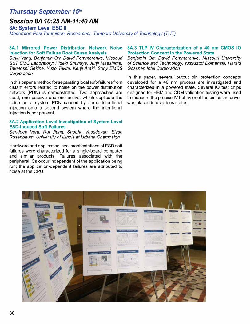
30
Session 8A 10:25 AM-11:40 AM8A: System Level ESD II Moderator: Pasi Tamminen, Researcher, Tampere University of Technology (TUT)
8A.1 Mirrored Power Distribution Network Noise Injection for Soft Failure Root Cause AnalysisSuyu Yang, Benjamin Orr, David Pommerenke, Missouri S&T EMC Laboratory; Hideki Shumiya, Junji Maeshima, Taketoshi Sekine, Yuzo Takita, Kenji Araki, Sony EMCS Corporation
In this paper a method for separating local soft-failures from distant errors related to noise on the power distribution network (PDN) is demonstrated. Two approaches are used, one passive and one active, which duplicate the noise on a system PDN caused by some intentional injection onto a second system where the intentional injection is not present.
8A.2 Application Level Investigation of System-Level ESD-Induced Soft Failures Sandeep Vora, Rui Jiang, Shobha Vasudevan, Elyse Rosenbaum, University of Illinois at Urbana Champaign
Hardware and application level manifestations of ESD soft failures were characterized for a single-board computer and similar products. Failures associated with the peripheral ICs occur independent of the application being run; the application-dependent failures are attributed to noise at the CPU.
Thursday September 15th
8A.3 TLP IV Characterization of a 40 nm CMOS IO Protection Concept in the Powered StateBenjamin Orr, David Pommerenke, Missouri University of Science and Technology; Krzysztof Domanski, Harald Gossner, Intel Corporation
In this paper, several output pin protection concepts developed for a 40 nm process are investigated and characterized in a powered state. Several IO test chips designed for HBM and CDM validation testing were used to measure the precise IV behavior of the pin as the driver was placed into various states.

31
Wor
ksho
ps
Workshops Chair: Guido Notermans <[email protected]>You are invited to send your comments/questions in advance to the respective workshop moderators via email at the ESDA web page (www.esda.org/events/eosesd-symposia/symposia/symposium-workshop-2/).
Session A: 5:30 p.m. - 7:00 p.m. (Parallel Sessions)A1. Should the Industry Council Address Adequate IEC 61000-4-2 Levels?Moderators: David Pommerenke, Missouri University of Science and Technology; Harald Gossner, Intel CorporationIndustry Council on ESD target Levels has reached its 10th anniversary. During this decade the group of more than 60 experts representing IC suppliers, system OEMs, ODMs, ESD control consultants and foundries has published 5 White papers on recommended HBM and CDM targets, the clarification of misconceptions of system level ESD protection and the recommendation of system efficient ESD design (SEED). The most recent document published in 2016 addresses the problem of EOS failures and EOS prevention. All White Papers have been adopted and endorsed both by ESDA and JEDEC. After this successful work over a decade the council is approached to provide support and direction settings in various fields. Some suggestions request an involvement of Industry Council in the question of adequate IEC 61000-4-2 levels. The workshop should help to formulate a recommendation to Industry Council to work in this direction. Is it time to perform an investigation similar to HBM and CDM regarding IEC standard and assess the real threat scenarios? What should be a proper gun test level to effectively protect electronic equipment in the end user’s home? This is a unique chance for a wide audience to steer the Industry Council activities.
A2. EOS Issues in Automotive Industry – What Information Needs to be Exchanged to Solve the Issue? Moderator: Reinhold Gaertner, Infineon Technologies, Joseph Ney, GM; James Roberts, Continental Automotive; Bob Knoell, NXP SemiconductorsEOS failures are a big problem in the industry. Especially in the automotive industry the root causes for these failures have to be investigated in a detailed way to avoid further issues in the future. But the physical failure analysis is only showing the consequence of the stress, but the real root cause cannot be determined without further information from the customer. To improve this situation a group of US car manufacturer started together with some Tier 1 and some semiconductor manufacturer a working group to define a process for the information flow between the various groups in case of an EOS issue. But what information is necessary and helpful to describe and solve EOS problems during manufacturing and in the field?
A3 . EDA ESD Verification Tools Utilized in Industry Today. Good, Bad, or Just Plain Ugly? Moderators: Robert Gauthier, GLOBALFOUNDRIES, Inc.; Stephen Fairbanks, SRF Technologies, LLCEDA checking/verification tools to design for effective on-chip ESD protection are getting used more and more. Come share what your experiences are in the field. Do you feel the tools identify the most important potential failures? Do the tools correlate with real-life failures? Do you find them useful or just a hassle? What more is needed to reduced/eliminate ESD design escapes/failures? Let’s collectively discuss and summarize what different types of checks are important and which design points we have good design/verification tools and which areas more is needed. Bring your experiences and thoughts/innovations.
TUESDAY SEPTEMBER 13TH

32
B1. Compliance Verification - TR 53 Moderators: John Kinnear, IBM; Ron Gibson, Advanced Static Control Consulting An ESD process relies on periodic measurements to ensure the controls continue to operate within defined parameters. In this workshop, the differences between qualification and compliance verification will be discussed. The requirements on the instrumentation and environmental requirements between qualification and compliance verification will be discussed. Verifying instrumentation, which is often overlooked, will also be discussed. Any issues with Compliance Verification or TR53 will be answered.
B2. High Pin Count ESD Device Qualification Moderators Wolfgang Stadler, Intel CorporationDuring the last decade, the average and maximum pin count of products has increased significantly. Particularly for products for communication and computing applications, pin counts of more than 2,000 are not rare. All current qualification standards have been developed when the pin count was typically an order of magnitude smaller, the application of these device testing standards to modern high-pin count products can cause severe problems. The testing time increases dramatically, but even worse, wear out by repeatedly stressing the same path and the increasing influence of tester parasitics can lead to unrealistic failures. In the workshop we want to discuss challenges of high pin-count ESD device testing, solutions, and possible future trends in the standardization of device testing. Some questions to discuss could be: Do we have an agreed standard for reducing the number of pin combinations? Is statistical pin testing a good approach? What about parasitics, two-pin testers, test times? How do we perform high pin-count CDM testing? What is the field relevance if one single weak pin fails in a high pin-count device?
B3. Correlation Between Component and System Level ESD Testing Moderator: Younes Benlakhoui, NXP Semiconductors; Harald Gossner, Intel CorporationA significant gap between component and system level test methods and standards is bridged. The system level standards, for example IEC 61000-4-2, have been developed to support ESD and EMI compliance qualification of the systems rather than to validate the passing level of IC components. The accomplished system design in general significantly impacts the ESD test results and pulse waveforms. However not only the system blocks, but also the PCB design are usually not finalized or communicated to the IC developers.Could be there any correlation of IC failure voltage to IEC failure voltage?What Happens When the discharge gets into the System? B4. EOS Analysis and Diagnosis - “Techniques and Methods for Dealing with EOS Induced Damage” New “World Cafe Style” Format! Moderators: Theo Smedes, Michael Stevens, NXP Semiconductors; David Eppes, AMDAlmost everyone faces the challenge of dealing with customer returns. Typically the pressure is large. What do you do with such returns?Can you immediately answer the burning questions like: is this ESD, is this EOS, is this ….?How do you do this? What is the role of Failure analysis in this process? What is the next most important part?This workshop will use a new format to create a brainstorm and discussion on these and similar questions with active audience participation.Don’t miss the opportunity to compare your methods to those of your peers!
Session B: 5:30 p.m. - 7:00 p.m. (Parallel Sessions)WEDNESDAY SEPTEMBER 14TH

33
You will find a broad spectrum of products and services for static protection, control, testing and analysis, as well as prominent trade publi-cations all in one location for your convenience. Exhibits are open to the public.
Exhibit HoursMonday, September 12th
Welcome Reception6:00 p.m. - 9:00 p.m.
Tuesday, September 13th
9:30 a.m. - 5:30 p.m.
Wednesday, September 14th
7:30 a.m. - 1:10 p.m.
10 minute showcase presentations from exhibitors are scheduled at the beginning of
select technical sessions.
A complimentary coffee bar is available in the exhibit hall for all who visit.
Tuesday lunch service will be available in the exhibit hall for anyone wishing to purchase
lunch while visiting the exhibits.
Attendee continental breakfast will be avail-able in the exhibit hall on Wednesday.
Exhi
bitsExhibitor Booth Number
ACL, Inc. 700Advanced Test Equipment Rentals Table – Foyer ANSYS 313Antistat, Inc. – The ESD Control Centre 514,516Asiatic Fiber Corporation 126Barth Electronics, Inc. 202Botron Co., Inc. 209 Carmel Olefins, BAZAN Group 525Conductive Containers, Inc. 309Core Insight, Inc. 210Dangelmayer Associates, LLC 506Desco Industries, Inc. 410Dou Yee Enterprises (S) Pte. Ltd. 411,413Electro-Tech Systems, Inc. 301ESDEMC Technology, LLC 404ESDMAN Co., Ltd. 114ESTION Technologies GmbH 508Euclid Vidaro Mfg., Co. 302ExtraTech Systems, LLC 226Gel-Pak/UltraTape 113Gibo|Kodama Chairs 304Grund Technical Solutions, Inc. 600Hanwa Electronic Ind. Co., Ltd. 505HPPI, GmbH 111IEEE EMC Society 400In Compliance Magazine 511Innovative Circuits Engineering, Inc. 104Integrated Packaging Films, Inc. 110iT2 Technologies, Inc. 314Julie Industries, Inc./StaticSmart Flooring 503Lubrizol 303Magwel 412,414Mentor Graphics 204Monroe Electronics, Inc. 402Moxtek, Inc. 504NRD-Staticmaster 510OnFILTER, Inc. 526Packaging & Crating Technologies 115PolyDrop, LLC 426Polyonics 203Premix Oy 214Presto Engineering 513Prostat Corporation 406RTP Company 401Shenzen Btree Industrial Co., Ltd. 212Shishido Electronics, Ltd. – Static Clean 502Sika Industrial Flooring 310Silicon Frontline Technology 107Simco-Ion 409STATICO 102Static Solutions, Inc. 512StaticStop, a division of SelecTech, Inc. 403Stephen Halperin & Associates, Ltd. 406TDI International, Inc. 213Tech Wear, Inc. 604Tek Stil Concepts, Inc. 101Thermo Fisher Scientific 602Transforming Technologies 103,105Trek, Inc. 201Zeon Chemicals L.P. 112
Publications and Associations ASM International Table – FoyerElectronics Protection Table – FoyerIEST Table – Foyer Interference Technology Table – FoyerPrinted Circuit Design & Fab/ Circuits Assembly Table – FoyerSMTA Table – Foyer

34
Technical Program CommitteeJames W. (Jim) Miller, NXP SemiconductorsDolphin Abessolo-Bidzo, NXP SemiconductorsRobert Ashton, On SemiconductorFabrice Caignet, LAAS-CNRSYiqun Cao, InfineonTechnologiesZhong Chen, University of Arkansas Shih-Hung Chen, imec Bernard Chin, UTAC Paolo Colombo, STMicroelectronicsPeter de Jong, Synopsys, Inc.Leonardo Di Biccari, STMicroelectronics Jeffrey Dunnihoo, Pragma DesignCharvaka Duvvury, ESD Consulting LLCDavid Eppes, AMD Kai Esmark, InfineonTechnologiesFarzan Farbiz, Texas Instruments, Inc.PhilippeGaly,STMicroelectronics EleonoraGevinti,STMicroelectronicsUlrichGlaser,InfineonTechnologiesNicolasGuitard,STMicroelectronics Nathan Jack, Intel CorporationDavid Johnsson, HPPI Michael Khazhinsky, Silicon Laboratories, Inc.Marcus Koh, Everfeed Technology Pte., Ltd. Jam-Wen Lee, TSMCYou Li, GLOBALFOUNDRIES, Inc.Dimitri Linten, imec Tim Maloney, Intel (Retired)Markus Mergens, QPXGmbHSouvick Mitra, GLOBALFOUNDRIES, Inc.Kiong Kay Ng, InfineonTechnologiesMototsugu Okushima, RenasasBenjamin Orr, Missouri University of Science and Technology Alan Righter, Analog Devices, Inc. Elyse Rosenbaum, University of Illinois at Urbana-ChampaignChristian Russ, Intel CorporationScott Ruth, NXP Semiconductors
EOS/ESD Association, Inc. OfficersPresidentGianluca Boselli, Texas Instruments, Inc., Dallas, TXSenior Vice PresidentGinger Hansel, Dangelmayer Associates LLC, Austin, TXVice PresidentAlan Righter, Analog Devices, Inc., Wilmington, MATreasurerJohn Kinnear Jr., IBM Corporation, Poughkeepsie, NYSecretaryHarald Gossner, Intel Corporation, Neubiberg, GERMANYPast PresidentTerry Welsher, Dangelmayer Associates LLC, Suwanee, GA
Headquarters OperationsLisa M. Pimpinella, Executive DirectorChristina Earl, Standards Sr. Program ManagerTerry Finn, Marketing Program ManagerNicholas Pimpinella, Administrative Assistant
Steering CommitteeGeneral Chair Melanie Etherton, NXP Semiconductors, Austin, TXVice General Chair Junjun Li, Apple, Cupertino, CATutorial Program Chair Wolfgang Stadler, Intel Corporation, Neubiberg, GERMANYTechnical Program Chair James W. (Jim) Miller, NXP Semiconductors, Austin, TX Workshops Chair GuidoNotermans,NXP Semiconductors, Hamburg, GERMANYArrangements Chair Cheryl Checketts, Scottsdale, AZRegistration Chair Raivo Leeto, Sandia National Laboratories, Albuquerque, NMAudio/Visual Co-Chair Lorenzo Cerati, STMicroelectronics, Agrate Brianza, ITALYAudio/Visual Co-Chair Wolfgang Stadler, Intel Corporation, Neubiberg, GERMANYTutorial Audio/Visual Chair Souvick Mitra, IBM Corporation, Essex Junction, VT Information David Swenson, AffinityStaticControlLLC,Austin,TXPast General Chair Warren Anderson, Synopsys, Inc., Boxborough, MAESDA Vice President Alan Righter, Analog Devices, Inc., Wilmington, MAPublications & Marketing HQ Operations, EOS/ESD Association, Inc., Rome, NY
Board of DirectorsGianlucaBoselli,Texas Instruments, Inc., Dallas, TXBrett Carn, Intel, Hillsboro, OR Lorenzo Cerati, STMicroelectronics, Agrate Brianza, ITALYCheryl Checketts, Scottsdale, AZCharvaka Duvvury, ESD Consulting LLC, Plano TXReinholdGaertner,InfineonTechnologies,Neubiberg,GERMANYHaraldGossner,IntelCorporation,Neubiberg,GERMANYGingerHansel,Dangelmayer Associates LLC, Austin, TX Matthew Hogan, MentorGraphics,Wilsonville,ORMichael Khazhinsky, Silicon Laboratories, Inc., Austin, TXJohn Kinnear Jr., IBM Corporation, Poughkeepsie, NYNathaniel Peachey, Qorvo,Greensboro,NCLisa Pimpinella, EOS/ESD Association, Inc., Rome, NYAlan Righter, Analog Devices, Inc., Wilmington, MAWolfgang Stadler, IntelCorporation,Neubiberg,GERMANYDavid Swenson, AffinityStaticControlLLC,Austin,TXScott Ward, Texas Instruments, Inc., Dallas, TXTerry Welsher, DangelmayerAssociatesLLC,Suwanee,GAJoshua Yoo, CoreInsight,Inc.,Seongnam-City,Gyeonggi-do,SOUTHKOREA
Symposium Committees
EOS/ESD Association, Inc.
Javier A. Salcedo, Analog Devices, Inc.Mirko Scholz, imec Mayank Shrivastava, Indian Institute of Science (IISc) BangaloreRaymond T. Sietereales, Analog Devices, Inc.Theo Smedes, NXP SemiconductorsWolfgang Stadler, Intel CorporationBernhard Stein, Intel CorporationYu-Ti Su, TSMC Teruo Suzuki, SocioNext Pasi Tamminen, Tampere University of Technology Augusto Tazzoli, Maxim Integrated Products, Inc.David Trémouilles, LAAS-CNRSJohan Van der Borght, SOFICS BVBA Vladislav Vaschenko, Maxim Integrated Products, Inc. Toni Viheriäkoski, Cascade Metrology Scott Ward, Texas Instruments, Inc.Richard Wong, Cisco Systems, Inc.

35
Board of DirectorsGianlucaBoselli,Texas Instruments, Inc., Dallas, TXBrett Carn, Intel, Hillsboro, OR Lorenzo Cerati, STMicroelectronics, Agrate Brianza, ITALYCheryl Checketts, Scottsdale, AZCharvaka Duvvury, ESD Consulting LLC, Plano TXReinholdGaertner,InfineonTechnologies,Neubiberg,GERMANYHaraldGossner,IntelCorporation,Neubiberg,GERMANYGingerHansel,Dangelmayer Associates LLC, Austin, TX Matthew Hogan, MentorGraphics,Wilsonville,ORMichael Khazhinsky, Silicon Laboratories, Inc., Austin, TXJohn Kinnear Jr., IBM Corporation, Poughkeepsie, NYNathaniel Peachey, Qorvo,Greensboro,NCLisa Pimpinella, EOS/ESD Association, Inc., Rome, NYAlan Righter, Analog Devices, Inc., Wilmington, MAWolfgang Stadler, IntelCorporation,Neubiberg,GERMANYDavid Swenson, AffinityStaticControlLLC,Austin,TXScott Ward, Texas Instruments, Inc., Dallas, TXTerry Welsher, DangelmayerAssociatesLLC,Suwanee,GAJoshua Yoo, CoreInsight,Inc.,Seongnam-City,Gyeonggi-do,SOUTHKOREA
Official Conference Hotel:Hyatt Regency Orange County
11999 Harbor Blvd. Garden Grove (Anaheim), California, USA, 92840 All reservations must be received by August 17, 2016
Room Rates$129 per night (Single, Double, Triple or Quad occupancy)
Phone Reservation – +1-888-421-1442
• Book reservations by 8/17/2016 (Please book early as a limited number of hotel rooms are available)
Reservations Link:
https://resweb.passkey.com/go/ESDA2016
Credit card is required to make reservations, credit card information accepted via phone or online.
Acc
omm
odat
ions
DESCRIPTIONLocated just 1 mile from the Anaheim Convention Center, and 1.4 miles from the Disneyland® Resort, the Hyatt Regency Orange County near Anaheim offers shuttle service to and from the parks, and is in close proximity to Angel Stadium, the Honda Center, world-famous beach-es, and many other Orange County attractions.Each modern guestroom features an oversized work desk, iHome Stereo with iPod® docking station, laptop safe, large work desk, and many other amenities. The hotel’s recreational facilities offer something for everyone, from two outdoor heated pools, hot tubs and full-sized tennis and basketball courts, to preferred tee times at premier golf courses and a 24-hour StayFit™ gym. Visit our website at www.orangecounty.hyatt.com for more information on everything that the Hyatt Regency Orange County has to offer, including on-site amenities, local attractions, transportation options, and more.
ROOM SCAMS-PIRATES/POACHING NOTICE:There are companies obtaining registration lists from public sources-do not respond to these solicitations concerning room reservations. In order to secure a room at the Hyatt Regency Orange County you must book through the proper official channel as provide above.Housing block “pirates” now routinely “poach” event attendees and exhibitors!The pirating companies gather group’s contact information from published or online directories. They call attendees leaving the impression that they are “official” housing. They will also frequently cite an imminent sell-out of the block while urging you to secure housing immediately. Another tactic is to offer a room rate that is significantly less than the official rate. Please do not respond to these solicitations.
Guestrooms include the following amenities:• Iron / ironing board• Personal coffee maker complete with condiments• In-room Safe• iHome Stereo with iPod® docking station• Wired and Wi-Fi high-speed Internet• Individual digital climate control• Video Checkout
Parking rates at the Hyatt Regency Orange County:• $10 for Self parking • $27 for Valet parking
Policies:Tax Policy Occupancy tax is 14.5% plus 2.5% Garden Grove Tourism Improvement Direct Assessment Fee plus $2.00 CA Tourism Fee per night. Taxes are subject to change.
Cancellation PolicyCancellation Policy is 72 hours prior to arrival (by 4pm, 3 days prior to arrival)
We would like to extend a special thank you to all our attendees and exhibitors that reserved a room at the Hyatt Regency Orange County through the ESDA room block. In order to secure the meeting and exhibit space required to hold this symposium and all ESDA events, hotels require that the association commits to fill a minimum number of sleeping rooms. If we do not fill these rooms we must pay, out of our association reserves, the full rate for each room left unoccupied. This fee directly impacts the amount we must charge you to attend the symposium as well as membership dues and other ESDA educational opportunities. Help us keep costs down by continuing to stay at our host hotel in the future. We greatly appreciate your support of the association.

EOS/ESD Symposium September 11-16, 2016 Hyatt Regency Orange County, Garden Grove (Anaheim), CA, USA
1 Please Print or Type (Your name and company will appear on badge and/or certificate exactly as written below.)
Registration - page 1
Under the Americans With Disabilities Act, I require auxiliary aids or services.IamtakingtheESDCertifiedProfessional-ProgramManagerexam:9-16-16.IamtakingtheESDCertifiedProfessional-DeviceDesignexam:9-16-16.
2 Tutorial & Seminar Registration
36
Please fill out all sections (1 thru 4) of this form. Sections 3 and 4 are on page 2.
Please continue and fill out all sections (3 and 4) of this form on page 2
Register Online!www.esda.org/events/eosesd-symposia/
Mr/Mrs/Ms/Dr First Name Last Name
Mailing Address/Street
Company Name Mail/Stop
City State/Province
Zip/Postal Code Country
Telephone Number Ext. Email Address
Address is company or home (check one)
Check each session attending, one session per time slot. For an overview of tutorial tracks see page 11SUNDAY, SEPTEMBER 11 & MONDAY, SEPTEMBER 12
FC340 8:00 a.m. - 5:00 p.m ESD Program Development and Assessment (ANSI/ESD S20.20 Seminar) (PrM) SUNDAY, SEPTEMBER 11, 2016
FC100: 8:00 a.m. - 5:00 p.m. ESD Basics for the Program Manager (PrM) DD110: 8:30 a.m. - 12:00 p.m. ESD from Basics to Advanced Protection Design (DD) DD200: 8:30 a.m. - 12:00 p.m. Charged Device Model Phenomena, Design,
and Modeling (DD) DD211: 8:30 a.m. - 12:00 p.m. EOS/ESD Failure Models and Mechanisms (DD) DD/FC122: 8:30 a.m. - 12:00 p.m. Use of the Digital Sampling Oscilloscope for ESD
Measurements DD/FC230: 8:30 a.m. - 12:00 p.m. System Level ESD/EMI: Principles, Design
Troubleshooting, and DemonstrationsI DD201: 1:00 p.m. - 4:30 p.m. ESD Protection and I/O Design DD204: 1:00 p.m. - 4:30 p.m. ESD Design in HV Technologies REVISED DD240: 1:00p.m.-4:30p.m. ESDDeviceQualificationTestingREVISED FC165: 1:00 p.m. - 4:30 p.m. Novel Methods for Fixing ESD Issues in the Factory for
Both Electronics & Explosive Products FC215: 1:00 p.m. - 4:30 p.m. Device Technology and Failure Analysis Overview
(PrM) REVISEDMONDAY, SEPTEMBER 12, 2016
FC101: 8:30 a.m. - 4:30 p.m. How To’s of In-Plant ESD Auditing and Evaluation Measurements (PrM)
DD/FC130: 8:30 a.m. - 12:00 p.m. System Level ESD/EMI Testing to IEC & Other Standards (PrM, DD,) NEW/REVISED
DD100: 8:30 a.m. - 12:00 p.m. ESD Circuits FC360: 8:30 a.m. - 12:00 p.m. Electrical Overstress (EOS) in Manufacturing and Test FC120: 8:30 a.m. - 12:00 p.m. Air Ionization Issues and Answers for the Program
Manager (PrM) DD300: 8:30 a.m. - 10:00 a.m. Circuit-Level Modeling and Simulation of On-Chip
Protection (DD) DD318: 10:30 a.m. - 12:00 p.m. FinFET and Advanced CMOS Technology ESD
TCAD Simulation DD231: 1:00 p.m. - 4:30 p.m. Integrated ESD Device and Board Level Design REVISED DD311: 1:00 p.m. - 4:30 p.m. Impact of Technology Scaling on Components High Current
Phenomena and Implications for Robust ESD Design (DD) REVISED
DD302: 1:00 p.m. - 4:30 p.m. Troubleshooting On-Chip ESD Failures (DD) DD/FC155: 1:00 p.m. - 4:30 p.m. ESD Control Workstations: Set-up, Practical Considerations
and Measurements NEW FC362: 1:00 p.m. - 4:30 p.m. Using Different Air Ionization Technologies and
Measuring Process Effects
EMERGINGTOPICS 1:00 p.m. - 2:30 p.m. PCB Design for Real-World EMC Control NEW 3:00 p.m. - 4:30 p.m. Radiated Emissions, Understanding Product and Measurement Antenna Behavior NEWTHURSDAY, SEPTEMBER 15, 2016
FC390: 8:30 a.m. - 4:30 p.m. Basics of ESD Process Assessment NEW FC170: 8:30 a.m. - 4:30 p.m. ANSI/ESD S20.20 – ESD Program Assessment for Internal
Auditors and Supplier Quality Engineers FC361: 8:30 a.m. - 12:00 p.m. Class 0A Devices & Boards - ESD Controls and Auditing
Measurements DD117: 8:30 a.m. - 10:00 a.m. TCAD Fundamentals DD112: 8:30 a.m. - 10:00 a.m. Latch-up Fundamentals (DD) DD102: 10:30 a.m. - 12:00 p.m. On-Chip ESD Protection in RF Technologies (DD) DD213: 10:30 a.m. - 12:00 p.m. ESD, EOS and Latch-up Failure Analysis for Designers DD220: 1:00 p.m. - 4:30 p.m. Transmission Line Pulse (TLP) Basics and Applications (DD) FC115: 1:00 p.m. - 4:30 p.m. Contamination & ESD Issues in Flat Panel Display
Manufacturing Process DD382: 1:00 p.m. - 2:30 p.m. Electronic Design Automation (EDA) Solutions for
Latch-up NEW DD322: 3:00 p.m. - 4:30 p.m. Advanced Latch-up Testing, Failure Analysis and Prevention
by Design Constraints and Tools

EOS/ESD Symposium September 11-16, 2016 Hyatt Regency Orange County, Garden Grove (Anaheim), CA, USA
Under the Americans With Disabilities Act, I require auxiliary aids or services.IamtakingtheESDCertifiedProfessional-ProgramManagerexam:9-16-16.IamtakingtheESDCertifiedProfessional-DeviceDesignexam:9-16-16.
Please Print or Type
Registration - page 2
Include payment with this form. Mail form and payment to: EOS/ESD Association, Inc., 7900 Turin Road, Bldg. 3, Rome, NY 13440-2069, USA, Tel: +1-315-339-6937. Students must include proof of full-time enrollment to obtain student fees. Only U.S. currency, checks drawn on a U.S. bank that is a member of the U.S. Federal Reserve, travelers checks payable in U.S. dollars, and credit cards (Visa®, Master Card®, AMEX®, and Discover®) will be accepted. Pick up registration materials at the Registration Desk when you arrive. Cancellation & refund requests will be honored if received in writing no later than July 21, 2016, and are subject to a $50 fee. Any other approved dispositions will also be assessed a $50 fee.
3 Fees: Please check appropriate boxes
Check (Make payable to EOS/ESD Association, Inc.)
TOTAL ENCLOSED $
Type: __Visa® __Master Card ® __AMEX® __Discover®
Credit Card # Expiration Date: Security Code (CVV):
Print Name on Card:
Billing Address: City State Zip
Remember to fill out sections 1 and 2 on page 1 of this form.
4 Payment • Company purchase orders not accepted.
Register Online!www.esda.org/events/eosesd-symposia/
Register online at www.esda.org/events/eosesd-symposia/
Technical Session Recording See page 22 for more Information Attendee/University Professional/Student $50 each
Save by registering in advance! This will facilitate your registration upon your arrival at the Symposium. Early registration and member discounts* are valid only if received no later than July 21, 2016.
*Membership discounts apply to those who participate as members all year long and are current at the opening of symposium registration. Memberships processed after this date will not apply. You will receive a complimentary 2017 membership with your Symposium registration which will allow you to enjoy the full benefits of membership in 2017.
Student FeesThe EOS/ESD Symposium offers a fifty percent discount for full-time students. Proof of enrollment required. Student fees apply only to symposium or tutorial registration and do not apply to bundled fees, ANSI/ESD S20.20 seminar, or Emerging Topics.
Symposium $800 (Includes technical sessions, workshops, and exhibits) Early Registration Fees valid until July 21, 2016EOS/ESD Association, Inc. Members* $600/Non-Members $700
Tutorials $710 (Sunday, Monday, OR Thursday (Full Day)) Early Registration Fees valid until July 21, 2016EOS/ESD Association, Inc. Members* $510/Non-Members $610
Bundled Fees $2,465 (Symposium plus Sun., Mon., and Thurs. full tutorial days) Early Registration Fees valid until July 21, 2016EOS/ESD Association, Inc. Members* $1,785/Non-Members $2,165
ESD Program Development and Assessment (ANSI/ESD S20.20 Seminar) $1,710(Attendance limited to first 30 registrants)This seminar is not included in the bundled fee. Early Registration Fees valid until July 21, 2016EOS/ESD Association, Inc. Members* $1,510/Non-Members $1,610 Register 5 or more people from one company at the same time and
save $100 per person. Please contact the EOS/ESD Association, Inc. prior to registering.
Emerging Topics $95 (Attendance limited to first 50 registrants) These seminars are not included in the bundled fee.
EOS/ESD Symposium September 11-16, 2016 Hyatt Regency Orange County, Garden Grove (Anaheim), CA, USA
Mr/Mrs/Ms/Dr First Name Last Name
Telephone Number Ext. Email Address
37