Embed Size (px)
Citation preview

SAND REPORTSAND2002-8075Unlimited ReleasePrinted February 2002
The Fabrication of Stainless Steel Partsfor MEMs
Terry Garino, Alfredo Morales, Thomas Buchheit, and Brad Boyce
Prepared bySandia National LaboratoriesAlbuquerque, New Mexico 87185 and Livermore, California 94550
Sandia is a multiprogram laboratory operated by Sandia Corporation,a Lockheed Martin Company, for the United States Department ofEnergy under Contract DE-AC04-94AL85000.
Approved for public release; further dissemination unlimited.

Issued by Sandia National Laboratories, operated for the United States Departmentof Energy by Sandia Corporation.
NOTICE: This report was prepared as an account of work sponsored by an agency ofthe United States Government. Neither the United States Government, nor anyagency thereof, nor any of their employees, nor any of their contractors,subcontractors, or their employees, make any warranty, express or implied, or assumeany legal liability or responsibility for the accuracy, completeness, or usefulness of anyinformation, apparatus, product, or process disclosed, or represent that its use wouldnot infringe privately owned rights. Reference herein to any specific commercialproduct, process, or service by trade name, trademark, manufacturer, or otherwise,does not necessarily constitute or imply its endorsement, recommendation, or favoringby the United States Government, any agency thereof, or any of their contractors orsubcontractors. The views and opinions expressed herein do not necessarily state orreflect those of the United States Government, any agency thereof, or any of theircontractors.
Printed in the United States of America. This report has been reproduced directlyfrom the best available copy.
Available to DOE and DOE contractors fromU.S. Department of EnergyOffice of Scientific and Technical InformationP.O. Box 62Oak Ridge, TN 37831
Telephone: (865)576-8401Facsimile: (865)576-5728E-Mail: [email protected] ordering: http://www.doe.gov/bridge
Available to the public fromU.S. Department of CommerceNational Technical Information Service5285 Port Royal RdSpringfield, VA 22161
Telephone: (800)553-6847Facsimile: (703)605-6900E-Mail: [email protected] order: http://www.ntis.gov/ordering.htm
3
SAND2002-8075Unlimited Release
Printed February 2002
The Fabrication of Stainless Steel Parts for MEMs*
Terry Garino, Alfredo Morales1, Thomas Buchheit2 and Brad Boyce2
Ceramic Materials and 2Tribology, Mechanics and Melting DepartmentsSandia National Laboratories
Albuquerque, NM 87185-1411, U.S.A.1Microsystems Processing Department, Sandia National Laboratories
Livermore, CA 94550, U.S.A.
AbstractA micro-molding process was used to fabricate parts in the 0.1 to 10 mm size range from astainless steel nano-powder. The two types of molds used were both produced from partsfabricated using the LIGA process so that they had precise dimensional tolerance and straightsidewalls. Rigid PMMA molds were made by injection molding and flexible silicone rubbermolds were made by casting. Mold filling was accomplished by mixing the powder with epoxyto form a putty-like material that was then pressed into the mold cavities and allowed to cure.After pyrolysis of the epoxy, the parts were sintered in forming gas. The densification kineticswere measured in situ using a video system. Full densification was achieved after 1 hour at1350�C. The microstructure of the sintered parts was examined using the SEM. The hardness,dimensional tolerance and surface roughness of the sintered parts were also measured.
* This paper was also submitted for publication in the proceedings of Symposium B (MaterialsScience of Microelectromechanical Systems Devices IV) of the Fall 2001 MRS Meeting.

4
ACKNOWLEDGMENT
Sandia National Laboratories is a multiprogram laboratory operated by Sandia
Corporation, a Lockheed Martin Company, for the United States Department of Energy under
Contract DE-ACO4-94AL85000. The authors would like to thank to Linda Domeier for
developing the PMMA molds, Dale Zschiesche and Marlow Weston for technical support, and
Gary Zender for scanning electron microscopy.

5
TABLE OF CONTENTS
Page
Introduction 7
Experimental Procedure 8
Results and Discussion 12
Conclusions 18
References 18

6
This page intentionally left blank

7
The Fabrication of StainlessSteel Parts for MEMs
Introduction
The two most common techniques for producing parts for MEMs, silicon surface
micromachining and LIGA, have limitations. Two limitations of Si micromachining are
composition and thickness. The available materials set includes only Si, SiO2, SiC and diamond.
Part thickness is generally in micron range. For the LIGA process, the materials set is limited to
materials that can be plated such as pure metal and some simple alloys. Plating is a slow process
and generates considerable quantities of hazardous waste. Thus an economical technique that
could produce parts of more complex metals as well as ceramics and polymeric materials would
complement the existing techniques.
One technique with the potential to fabricate parts for MEMs with precise dimensional
tolerance and with a very broad materials set is micro molding. In micro molding, a micro-mold
is first fabricated that has cavities that are the shape of the desired parts. The mold cavities are
then filled with the material of interest, typically in powdered form. The parts are then released
from the mold and sintered to achieve high density and strength. Since it is a batch process,
micro molding has the potential to be low cost, as long as the cost of the molds is not excessive.
Previous work has focused on either powder injection molding1-4, a more complicated process, or
on filling molds made by deep x-ray lithography (DXRL) 5, the same process used to make
molds for LIGA, which were therefore relatively expensive due to the cost of synchrotron
exposure. In the present work, LIGA was used to make the master from which the molds are
made so that precise dimensional tolerance, straight sidewalls and high aspect ratio parts can be
produced without the expense of DXRL.

8
Experimental Procedure
Two types of micro-molds were used. The first type, shown in Figure 1a, was made by
injection molding of poly(methyl) methacrylate (PMMA) using a nickel master that had been
made by the LIGA process. These molds were rigid and had cavities of either 90 or 170 �m
deep. The cavities ranged from several mm to several hundred microns with the smallest
features in the 10 �m size range. The same pattern was used for the flexible silicone rubber
molds. The silicone rubber resin was cast over the nickel master and allowed to cure (see Figure
1b). Molds with cavities up to 400 �m deep were produced.
(a) (b)
Figure 1. Images of micro-molds. (a) SEM image of PMMA mold and (b) optical image ofsilicone rubber mold.
To be able to faithfully reproduce features in the 10 �m range using a powder, the
particles in the powder must be much finer than the minimum feature size. Commercial stainless
steel powders produced for powder metallurgy have average particle sizes of 15 �m or larger and
are therefore unsuitable for this application. Therefore, a specially prepared nano-powder of
316L stainless steel was used. This powder was made by a plasma process involving the electro-
2 mm

9
explosion of metal wire (Argonide, Sanford, FL) and had particles in the hundred-nanometer
range.
A variety of techniques were investigated for filling the mold cavities with the powder.
These techniques can be divided into three groups: dry, semi-dry and wet. The dry techniques
included dry pressing and tape embossing. For dry pressing, the powder was first dispersed in a
solvent that contained a binder then dried and granulated. The granules were then applied in a
layer on top of the PMMA mold and uniaxially pressed at 25 MPa using a sheet of polyurethane
between the die ram and the granules to help transfer the pressure into the cavities. The parts
were then de-molded by partially dissolving the mold in methylene chloride. A problem with
this process was that inter-granule porosity was difficult to eliminate because of the low-pressure
limitation of the PMMA mold.
The wet process involved making a dispersion of the powder in a solvent containing
dissolved binder and then applying the dispersion to the mold surface and allowing it to dry.
One problem with this process was the tendency to entrap tiny air bubbles, especially in small
features in the mold. Also, cracking during drying was a problem especially for thicker parts and
for nano-sized powders.
Because of the problems with the other techniques, a semi-dry process was developed
and used for the rest of this work. In this process, epoxy was used as a curable binder so that the
mold could be filled when the epoxy was fluid and then de-molding could be done after the
epoxy cured and was thus stronger and insoluble. In this process, the powder was first dispersed
in methyl ethyl ketone (MEK) using a dispersant (Disperbyk-180, Byk-Chemie, Wallingford,
CT) and an ultrasonic horn. The epoxy resin (Shell 815) was then added (1g per 8 g of powder)
and the MEK was removed by evaporation, thus producing a homogeneous mixture of the
powder and the resin. The curing agent (TETA) was then added (0.125 ml per g of resin) and
mixed in using a mortar and pestle until the mixture resembled putty. The mixture was then
pressed onto either type of mold. The mixture could be removed from the mold as a sheet with
the parts on one face when the epoxy had cured to the leathery stage. If the epoxy was allowed
to fully cure in the PMMA molds, the excess could be sanded off, leaving the cavities fully filled
as shown in Figure 2. These parts could then be released using methylene chloride.

10
(a)
(b)
©
Figure 2. Optical micrographs of PMMA micro-molds with 90 �m deep cavities filled withstainless steel/epoxy: (a) top surface (b) top surface at higher magnification and(c) bottom surface taken looking through the mold.
0.5 mm0.5 mm
125 �m125 �m
0.5 mm0.5 mm

11
Prior to sintering, the epoxy binder had to by removed. To pyrolize the epoxy without
oxidizing the stainless steel, a low pO2 atmosphere produced by bubbling 3% hydrogen in argon
through room temperature water was used.
A video imaging system was used to measure the shrinkage of the molded parts during
sintering. The system had a closed tube with a window on one end to allow control of the
sintering atmosphere. A strobe illumination system (Control Vision, Idaho Falls, ID) was used
to be able to acquire high contrast images at high temperatures.
Sintered parts were characterized using SEM. Part distortion and part-to-part
dimensional variation were characterized using optical microscopy. A profilometer was used to
measure the average surface roughness. Hardness values were determined using instrumented
nanoindentation data collected on a Hysitron Triboscope with a 3-sided diamond Berkovich
indenter tip on a polished cross-section.

12
Results and Discussion
Figure 3 shows the structure of the starting powder stainless steel nano-powder. The particles
were spherical and mostly in the 100 to 200 nm size range, although there were occasional
particles up to 1 �m in size. In spite of its small particle size, the powder was quite stable with
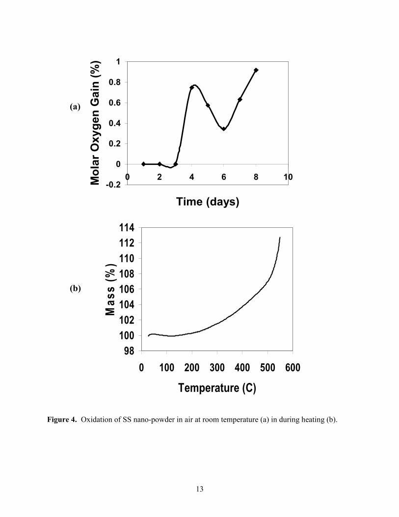
respect to oxidation. Figure 4a shows that at room temperature, oxidation starts after 3 days and
reaches about a 1% weight gain after a week. In Figure 4b the weight gain during heating at
10�C/min in air using the thermal gravimetric analysis system (Netzsch, Selb, Germany) is
shown. Oxidation starts above 200�C and is nearly complete around 550�C.
Figure 3. SEM images of Argonide strainless steel powder.
300 nm300 nm
500 nm500 nm
13
(a)
(b)
Figure 4. Oxidation of SS nano-powder in air at room temperature (a) in during heating (b).
-0.2
0
0.2
0.4
0.6
0.8
1
0 2 4 6 8 10
Time (days)
Mol
ar O
xyge
n G
ain
(%)
98100102104106108110112114
0 100 200 300 400 500 600
Temperature (C)
Mas
s (%
)
14
The linear shrinkage measured in situ using the video system is shown in Figure 5.
Shrinkage commenced around 1050�C and reached 19% at the start of the soak at 1350�C. An
additional 2% shrinkage occurred after an hour at 1350�C. From this amount of shrinkage, a
green density of 49% can be calculated, assuming theoretical density was achieved, as is shown
below. The low green density is the main reason that the sintering temperature required for
densification was higher than expected for a stainless steel with particles this small. Figure 6 is
an optical image of a sintered part from a PMMA mold that was held for 1 hr at 1350�C.

15
(a)
(b)
Figure 5. The shrinkage of a stainless steel micropart heated in 3% hydrogen. (a) during the
10�C/min ramp and (b) during the hold at 1350�C.
0
5
10
15
20
25
900 1000 1100 1200 1300 1400Temperature (C)
Shrin
kage
(%)
18.5
19
19.5
20
20.5
21
21.5
0 10 20 30 40 50 60 70Time (min)
Shrin
kage
(%)

16
Figure 6. Optical micrograph of sintered stainless steel micro-molded part from a PMMA mold.
The results of the SEM examination of the microstructure of sintered parts showed that at
1300�C, the particles were still rounded with an average size only slightly larger than the starting
particles size (see Figure 7). By 1350�C, the particles were well sintered together with only
closed porosity and a 0.5 �m average grain size. Further densification with only slight grain
growth occurred after 20 min at 1350�C so that nearly theoretical density was reached with the
average grain size less than 0.6 �m. Further heating at 1350�C resulted in rapid grain growth so
that the average grain size increased to 9 �m after 1 hr.

17
(a) (b)
© (d)
Figure 7. SEM micrographs of sintered stainless steel micro-molded parts: (a) 1300�C, 0 min,
(b) 1350�C, 0 min, (c) 1350�C, 20 min and (d) 1350�C, 1 hr.
1 �m1 �m1 �m 1 �m1 �m1 �m
1 �m1 �m1 �m1 �m1 �m1 �m1 �m

18
The nano-hardness of a part sintered at 1350C for 1 hr was 5 GPa, in line with
expectations. The average as-sintered surface roughness (1350°C/1hr) = 300 nm, which is much
less than the grain size. The average single part dimensional distortion = 0.45% and the average
part-to-part dimensional variation = 2.3%.
Conclusions
Stainless steel parts with features in the 0.01 mm range were fabricated by micro molding
of a nano-powder using molds replicated from LIGA-produced masters. Epoxy was used as a
curable binder to mold the parts and was removed by pyrolysis in forming gas. Parts were
sintered in hydrogen to high density at 1350�C with an average grain size of 0.6 �m. Sintered
parts had expected hardness values and reasonably smooth surfaces and small distortion. More
work needs to be done to improve part-to-part dimensional variation.

19
References
1. V. Piotter, T. Hanemann, R. Rupecht and J. Hausselt, Microsystem Technologies 3, 129(1997).
2. T. Hanemann, R. Rupecht and J. Hausselt, Adv. Mater. 9, 927 (1997).
3. V. Piotter, T. Benzler, T. Gietzelt, R. Rupecht and J. Hausselt, Adv. Engineering Mater. 2(639) (2000).
4. Z. Liu, N. Loh, S. Tor, K. Khor, Y. Murakoshi and R. Maeda, Mater. Let. 48, 31 (2001).
5. T.J. Garino, T. Christenson, and E. Venturini in Materials Science ofMicroelectromechanical Systems (MEMS) Devices, edited by A. H. Heuer and S. J. Jacobs,(Mater. Res. Soc. Proc. 546, Pittsburgh, PA, 1998) pp. 195-200.
6. Andrej Salak, Ferrous Powder Metallurgy (Cambridge International Science Publishing,Cambridge, 1995) pp. 273-5.
20
INITIAL DISTRIBUTION: 1 MS0885 D. B. Dimos, 1801 MS9403 W. R. Even, 87221 MS0887 M. J. Cieslak, 1800 MS9409 G. D. Kubiak, 8732 5 MS0889 B. L. Boyce, 1835 MS9409 J. Goldsmith, 87305 MS0889 T. E. Buchheit, 1835 MS9409 W. C. Replogle, 87311 MS0889 R. J. Salzbrenner, 18355 MS1411 T. J. Garino, 1843 3 MS9018 Central Technical Files,1 MS1349 J. Cesarano, 1843 8945-11 MS1349 K. G. Ewsuk, 1843 1 MS0899 Technical Library, 96161 MS1349 W. F. Hammetter, 1843 1 MS9021 Classification Office, 8511/
Technical Library, MS0899,1 MS9001 M. E. John, 8000; Attn: 9616
MS9002 P. N. Smith, 8500 DOE/OSTI via URLMS9003 K. E. Washington, 8900MS9004 J. Vitko, 8100MS9005 D. R. Henson, 8200MS9031 K. C. Olsen, 11600MS9054 W. J. McLean, 8300
1 MS9042 J. A. Crowell, 87271 MS9042 W-Y Lu, 87251 MS9401 J. M. Hruby, 87021 MS9401 D. E. McLean, 87291 MS9401 M. A. Bankert, 87295 MS9401 A. M. Morales, 87291 MS9401 R. Shediac, 87291 MS9401 C-Y P. Yang, 87291 MS9401 D. M. Skala, 87291 MS9401 R. P. Janek, 87291 MS9401 C. C. Henderson, 87291 MS9401 J. J. Kelly, 87291 MS9402 K. L. Wilson, 87241 MS9403 J. C. Wang, 87231 MS9403 N. Y. C. Yang, 87231 MS9404 S. H. Goods, 87251 MS9405 D. A. Hughes, 87261 MS9671 D. A. Chinn, 8729
1 MS9405 R. H. Stulen, 8700; Attn:MS9042 J. L. Handrock, 8727MS9042 M. F. Horstemeyer, 8728MS9161 E. P. Chen, 8726MS9161 R. Q. Hwang, 8721MS9401 J. R. Garcia, 8725MS9402 C. H. Cadden, 8724