Embed Size (px)
Citation preview

THE EFFECTS OF PRIOR NITRIDATION PROCESS OF SILICON SURFACE AND DIFFERENT METAL GATES ON THE
CAPACITANCE VOLTAGE CHARACTERISTICS OF METAL-TA2O5-SI MOS CAPACITOR
A Thesis Submitted to the Graduate School of Engineering and Sciences of
İzmir Institute of Technology in partial Fulfillment of the Requirements for the Degree of
MASTER OF SCIENCE
In Physics
by Eylem DURĞUN ÖZBEN
July 2007 İZMİR

We approve the thesis of Eylem DURĞUN ÖZBEN Date of Signature ……………………………… 28 September 2007 Prof. Dr. Mehmet GÜNEŞ Supervisor Department of Physics Muğla University ……………………………… 28 September 2007 Assist. Prof. Yusuf SELAMET Department of Physics İzmir Institute of Technology ……………………………… 28 September 2007 Assist. Prof. Habibe BAYHAN Department of Physics Muğla University
……………………………… 28 September 2007 Assoc. Prof. Lütfi ÖZYÜZER Head of Department İzmir Institute of Technology
…………………………… Prof. Dr. M. Barış ÖZERDEM
Head of the Graduate School

i
ACKNOWLEDGEMENTS
I would like to express my sincere appreciation to my advisor Prof. Dr. Mehmet
GÜNEŞ for his help and support during my Master of Science thesis. Without his
support I could not have possibly finished my study.
I also would like to thank to Prof. Dr. Elena Atanassova from Bulgarian
Academy of Science for supplying us the samples used in this thesis.
My sincere thanks are extended to members of Physics Department of Izmir
Institute of Technology (IYTE). In particular, my special thanks go to Prof. Dr. Durmuş
Ali DEMİR who provided invaluable assistance during my Master of Science study.
Sufficient thanks can not be given to my parents, to my mother, father and
especially to my husband Edip. Without their support it would have been impossible for
me to succeed in my study.
Finally, I would like to thank to all of my friends at IYTE especially to Yılmaz,
Beyhan and Önder for their encouragement during my graduate study.

ii
ABSTRACT
THE EFFECTS OF PRIOR NITRIDATION PROCESS OF SILICON SURFACE AND DIFFERENT METAL GATES ON THE
CAPACITANCE VOLTAGE CHARACTERISTICS OF METAL-TA2O5-SI MOS CAPACITOR
According to the 2004 International Technology Roadmap of Semiconductor
(ITRS), for sub-micron technology, an equivalent oxide thickness (EOT) less than 1 nm
is required. However, for such thickness levels, the native oxide SiO2 is unacceptable
since it does not posses its inherited physical properties and results in high leakage
current density resulting in reduced device performance. The replacement of SiO2 with
high dielectric constant material (high-k) may eliminate such problems since it will
allow the usage of thicker dielectric material. The leakage current will be reduced while
maintaining the same levels of inversion charge. In this study, the electrical properties
of metal-Ta2O5-Si MOS capacitor were investigated for devices prepared with different
conditions. A prior nitridation process of silicon surface in N2O and NH3 gas before
Ta2O5 was carried out to improve interface quality. In addition, different metal gates
formed on the Ta2O5 oxide layer were also used in order to see the effects of top oxide-
metal gate on the electrical properties of MOS capacitors. The metal gates used are Al,
TiN and W. High frequency (1MHz) Capacitance-Voltage Spectroscopy was used to
understand the effects of prior nitridation process and metal gates on the Ta2O5 high-k
oxide properties. From the analysis of high frequency C-V curves, oxide capacitance,
dielectric constant, EOT, leakage current density, conductance, flat band voltage VFB
shift, mobile charge density, effective oxide charge and interface trap density Dit were
obtained and compared with those of reference samples. Reference sample -1 has native
oxide SiO2 and Al metal gate and Reference sample-2 has Ta2O5 oxide layer with
unnitrided silicon surface.
It has been found that, the replacement of SiO2 gate oxide with Ta2O5 oxide
layer results in an increase in dielectric constant by several factors and using nitridation
process prior to Ta2O5 oxide layer improves the interface properties. Many promising
results were obtained for samples with W metal gates and nitrided silicon surface prior
to formation of Ta2O5 oxide layer. It is potentially applicable to future MOS devices.

iii
ÖZET METAL-Ta2O5-Si MOS KAPASİTÖRLERDE SİLİSYUM YÜZEYİNİN
ÖN NİTRÜRLEME İŞLEMİ VE FARKLI METAL KONTAKLARIN KAPASİTE GERİLİM KARAKTERİSTİKLERİNE ETKİLERİ
Yarı iletkenlerin uluslar arası teknoloji (ITRS) haritasının 2004 yılındaki
açıklamasına göre, mikron-altı teknoloji için, 1 nm den küçük eşdeğer oksit kalınlığına
(EOT) ihtiyaç vardır. Fakat bu kalınlıkta doğal SiO2 kendi fiziksel özelliklerini
koruyamadığından ve cihazın performansını düşüren yüksek akım kaçağına neden
olduğundan kullanım için pek uygun değildir. SiO2’ in daha yüksek dielectric sabitine
sahip bir yalıtkanla değiştirilmesi yukarıda bahsedilen problemleri azaltırken daha kalın
bir oksit tabakasının kullanımını sağlar. Bu da SiO2 ile aynı terslenim yük tabakasını
oluştururken kaçak akımı düşürecektir. Bu çalışmada farklı koşullarda hazırlanmış
metal-Ta2O5-si MOS kapasitörler incelenmiştir. Ara yüzey özelliklerini iyileştirmek için
oksit tabakasının büyütülmesinden önce silisyum yüzeyine N2O ve NH3 gaz
ortamlarında 700–850 oC sıcaklık aralığında ön nitrürleme işlemi uygulanmıştır.
Bununa beraber, metalin metal-oksit üst ara yüzeyinde MOS kapasitörlerin elektriksel
özellikleri üzerindeki etkisini incelemek üzere farklı metal elektrotlar kullanılmıştır.
Kullanılan metal elektrotlar sırasıyla Al, TiN ve W. Kullanılan farklı metallerin ve
nitrürleme işleminin MOS kapasitörlerin oksit ve ara yüzey üzerindeki etkilerini
incelemek için yüksek frekanslı (1MHz) Kapasitans-Gerilim spektroskopisi
kullanılmıştır. Yüksek frekansta ölçülen C-V eğrisinden yararlanarak, oksit kapasitansı,
dielektrik sabiti, EOT, kaçak akım yoğunluğu, düz bant gerilimi, histerisis kayması,
hareketli tuzak yükleri, etkin oksit yük yoğunluğu ve ara yüzey tuzak yoğunluğunu
içeren elektriksel özellikler hesaplanmış ve referans örnekleriyle kıyaslanmıştır.
Referans örnek-1, doğal oksit SiO2 ve Al metal gate içermekte ve Referans örnek-2
Ta2O5 oksit ve nitrürlenmemiş silisyum yüzeyi içermektedir.
Sonuç olarak, Ta2O5’ in SiO2’in yerine kullanılmasıyla dielektrik sabitinin
birkaç kata kadar artığı ve ön nitrürleme işleminin ara yüzeyi daha iyi bir hale getirdiği
gözlenmiştir. Tungsten metaline ve Ta2O5 oksidin büyütülmesinden önce ön nitrürleme
işlemine maruz bırakılmış silisyum yüzeyine sahip örneklerde umut verici sonuçlar
bulunmuştur. İleride yapılacak olan MOS cihazlarda kullanılabilir.

iv
TABLE OF CONTENTS
LIST OF FIGURES…………………………………….................................................vi
LIST OF TABLES …………………………………………………………………xiv
CHAPTER 1. INTRODUCTION………………………………………………………1
1.1. Thesis Objective………………………………………………………14
CHAPTER 2. EXPERIMENTAL……………………………………………………...16
2.1. Sample preparation……………………………………………………16
2.2. Characterization Techniques………………………………………….20
2.2.1. Capacitance-Voltage (C- V) Spectroscopy……………………….20
CHAPTER 3. PHYSICS OF MOS CAPACITORS AND ANALYSIS……………….30
3.1. Ideal MOS Capacitor………………………………………………….30
3.2. Theoretical Capacitance of Ideal MOS Structure……………………..36
3.3. Non-Ideal MOS Capacitor…………………………………………….43
3.3.1. Non-Ideal Effect…………………………………………………..43
3.3.2. Calculation of Flat Band Voltage, Doping concentration and
the effective oxide charge…………………………………………46
3.3.3. Extraction of Density of Interface Trap States (Dit)………………50
3.3.3.1. High Frequency Capacitance-Voltage Method
(Terman’s Method)…………………………………………...50
3.3.3.2. Combined High-Low Frequency Capacitance Method……53
CHAPTER 4. EXPERIMENTAL RESULTS………………………………………….56
4.1. Introduction…………………………………………………………...56
4.2. Results of Al-SiO2-Si MOS capacitor; Reference Sample-1…………57
4.3. Results of Al-Ta2O5-(SiO2)-Si MOS capacitor; Reference
Sample-2………………………………………………………………64
4.4. The Effect of Prior Nitridation of Silicon Surface……………………71
4.4.1. Prior Nitridation of Silicon Surface in N2O Gas Ambient………...71
4.4.2. Prior Nitridation of Silicon Surface in NH3 Gas Ambient………...89

v
4.4.3. Conclusion………………………………………………………102
4.5. Results of Metal-Ta2O5-(SiO2)-Si MOS Capacitor; The Effect
of Metal Gates……………………………………………………….103
4.5.1. Results of Al-Ta2O5-(SiOxNy)-(SiO2)-Si MOS Capacitor……….104
4.5.2. Results of TiN-Ta2O5-(SiO2)-Si MOS Capacitor………………..109
4.5.3. Results of W-Ta2O5-(SiOxNy)-Si MOS Capacitor……………….116
4.5.4. Conclusion……………………………………………………….125
CHAPTER 5. DISCUSSIONS AND CONCLUSIONS………………………………127
5.1. Future Work...………………………………………………………..139
REFERENCE…………………………………………………………………………140

vi
LIST OF FIGURES
Figure Page
Figure 1.1. Illustration of Moore’s law…………………………………………………..1
Figure 1.2. Work function of metal candidates………………………………………...13
Figure 2.1. Construction of metal-oxide-semiconductor MOS capacitors
used in this thesis ………………………………………………………….19
Figure 2.2. Block diagram of simultaneous Capacitance-Voltage measurement
system used in this thesis……………………………………………………22
Figure 2.3. Default values stored in material constant…………………………………23
Figure 2.4. Main menu and startup banner……………………………………………..24
Figure 2.5. Set IEEE address window………………………………………………….24
Figure 2.6. Model 82 calibration source value entry window………………………….25
Figure 2.7. Calibrate/ Send constants window…………………………………………25
Figure 2.8. Model 82 main menu………………………………………………………27
Figure 2.9. Device characterization menu……………………………………………...27
Figure 2.10. Parameter selection menu………………………………………………...28
Figure 2.11. High and low frequency C-V graphic of MOS capacitor………………...28
Figure 2.12. Device measurement and analysis menu…………………………………29
Figure 2.13. Data analysis menu……………………………………………………….29
Figure 3.1. Structure of an MOS capacitor…………………………………………….31
Figure 3.2. Energy-band diagrams for a p-type MOS capacitor at thermal
Equilibrium………………………………………………………………..32
Figure 3.3. Energy band diagram of MOS capacitor in accumulation region…………34 Figure 3.4. Energy band diagram of MOS capacitor in depletion region……………...34
Figure 3.5. Energy band diagram of MOS capacitor at the threshold point……………35
Figure 3.6. Energy band diagram of MOS capacitor in the inversion region…………..36
Figure 3.7. Schematic representation of the MOS capacitor as a series
combination of Cox and CSi…………………………………………………39
Figure 3.8. Variation of the space charge density SiQ' in the semiconductor
as a function of the surface potential sψ for a p-type Si with

vii
−AN =1.2x10¹⁵ at room temperature………………………………………..42
Figure 3.9. Normalized Theoretical ideal MOS structure C-V curve for
accumulation, depletion and inversion region……………………………...44
Figure 3.10. Terminologies for the names and location of charges in
Metal-Oxide-Si system................................................................................46
Figure.3.11. 1/C2 versus VG curve of a MOS capacitor………………………………..48
Figure 3.12. Theoretical and experimental high Frequency C-V curves of a
MOS capacitor with p-type silicon substrate……………………….....49
Figure.3.13. Counter-clockwise hysteresis characteristics of MOS capacitor………...51
Figure 3.14 A theoretical C/Cox vs ψs compared with an experimental C/Cox
vs VG for a MOS capacitor………………………………………..52
Figure 3.15. The surface potential ψs versus gate voltage VG obtained from the
theoretical and experimental high frequency C/Cox curves of a MOS
capacitor shown in Figure 3.13…………………………………………....53
Figure 3.16. Density of interface trap states, Dit, as a function of energy in the
band gap of crystalline silicon obtained from Figure 3.15………………..54
Figure 3.17. Combined High-low frequency C-V curves for native SiO2 sample……..56
Figure 3.18. Density of interface trap states, Dit, as a function of energy
in the band gap of crystalline silicon obtained from Terman’s
method and Combined High-low frequency Capacitance method
for sample with SiO2 oxide layer………………………………………….57
Figure 4.1. Experimental High-Low frequency capacitance versus gate
voltage curves of Al- SiO2-Si MOS capacitors; reference sample…………60
Figure 4.2. Forward and reverse C-V curve of Al- SiO2-Si MOS capacitor
with unnitrided Si surface ………………………………………………….60
Figure 4.3. Experimental 1/C2 versus gate voltage VG
graph of four different
dots of Al-SiO2-Si MOS capacitor………………………………………....62 Figure 4.4. Normalized experimental and theoretical capacitance versus gate
voltage and conductance versus gate voltage of Al-SiO2-Si MOS
capacitor …………………………………………………………………...62
Figure 4.5. The surface potential ψs versus gate voltage VG obtained from the
normalized theoretical and experimental high frequency C/Cox-V
curves of Al- SiO2-Si MOS capacitor……………………………………..64
viii
Figure 4.6. Density of interface states as a function of energy in the band
gap of crystalline silicon for four different dots of Al- SiO2-Si MOS
capacitor……………………………………………………………………..64
Figure 4.7. J-V characteristics of Al- SiO2-Si MOS capacitor; reference sample-1…...65
Figure 4.8. High frequency capacitance versus gate voltage curves of
Al-Ta2O5-(SiO2)-Si MOS capacitors……………………………………….67
Figure 4.9. Forward and reverse C-V curve of Al-Ta2O5-(SiO2)-Si MOS capacitor
with unnitrided Si surface…………………………………………………..67
Figure 4.10. Experimental 1/C2 versus gate voltage VG
graph of four different
dots of Al-Ta2O5-(SiO2)-Si MOS capacitor……………………………….69 Figure 4.11. Normalized experimental and theoretical capacitance versus gate
voltage and conductance versus gate voltage of Al-Ta2O5-Si MOS
capacitor…………………………………………………………………...69 Figure 4.12. J-V characteristics of Al-Ta2O5-(SiO2)-Si MOS capacitor, reference
sample-2 and reference sample-1……………………………………........70
Figure 4.13. The surface potential ψs versus gate voltage VG obtained from the
normalized theoretical and experimental high frequency C/Cox-V
curves of Al-Ta2O5-(SiO2)-Si MOS capacitor…………………………….72
Figure 4.14. Density of interface states as a function of energy in the band gap
of crystalline silicon for four different dots of Al-Ta2O5-(SiO2)-Si
MOS capacitor……………………………………………………………..72
Figure 4.15. High frequency capacitance versus gate voltage curves of
Al-Ta2O5-(SiOxNy)-Si MOS capacitors for nitridation temperatures
at 700°C in N2O gas environment………………………………………...75
Figure 4.16. Forward and reverse C-V curve of Al-Ta2O5-(SiOxNy)-Si MOS
capacitor with nitrided Si surface at 700 oC in N2O for two MOS
capacitor obtained on the same substrate…………………………………77
Figure 4.17. Experimental 1/C2 versus gate voltage VG
graph of four different
dots of Al-Ta2O5-(SiOxNy)-Si MOS capacitor for nitridation
temperature at 700°C in N2O gas environment……………………….78
Figure 4.18. Normalized experimental and theoretical capacitance versus

ix
gate voltage and conductance versus gate voltage of Al-
Ta2O5-(SiOxNy)-Si MOS capacitor prepared after nitridation
process in N2O at 700°C…………………………………………………. 78
Figure 4.19. J-V characteristics of Al-Ta2O5-(SiOxNy)-Si MOS capacitor prepared
after nitridation process at 700oC in N2O and that of the reference
sample-1……………………………………………………………………79
Figure 4.20. The surface potential ψs versus gate voltage VG obtained from the
normalized theoretical and experimental high frequency C/Cox-VG
curves of reference samples-1,2 and Al-Ta2O5-(SiOxNy)-Si MOS
capacitor prepared after nitridation process in N2O at 700oC…………….81 Figure 4.21. Density of interface states as a function of energy in the band gap
of crystalline silicon for four different dots of Al-Ta2O5-(SiOxNy)-
Si MOS capacitor prepared after nitridation process in N2O at 700oC……81
Figure 4.22. Experimental high frequency capacitance-voltage curves of four
different dots of Al-Ta2O5-(SiOxNy)-Si MOS capacitor prepared
after nitridation process in N2O at a) 800°C, b) 850°C…………………...83
Figure 4.23. Forward and reverse C-V curve of Al-Ta2O5-(SiOxNy)-Si MOS
capacitor with nitrided Si surface in N2O at a) 800oC, b) 850oC…………84
Figure 4.24. Experimental 1/C2 versus gate voltage VG
graph of four different
dots of Al-Ta2O5-(SiOxNy)-Si MOS capacitor for nitridation
temperature at a) 800 °C b) 850°C, in N2O gas environment……………..86
Figure 4.25. Normalized experimental and theoretical capacitance versus gate
voltage and conductance versus gate voltage of Al-Ta2O5-(SiOxNy)-
Si MOS capacitor prepared after nitridation process in N2O at a)
800 °C b) 800°C…………………………………………………………..87
Figure 4.26. J-V characteristics of Al-Ta2O5-(SiOxNy)-Si MOS capacitor prepared
after nitridation process at a) 800oC, b) 850oC, in N2O with that of
reference sample-1 and reference sample-2………………………………88
Figure 4.27. The surface potential ψs versus gate voltage VG obtained from the
normalized theoretical and experimental high frequency C/Cox vs VG
curves of Al-Ta2O5-(SiOxNy)-Si MOS capacitor prepared after
nitridation process in N2O at a) 800oC, B) 850oC………………………...90

x
Figure 4.28. Density of interface states as a function of energy in the band gap
of crystalline silicon for four different dots of Al-Ta2O5-
(SiOxNy)-Si MOS capacitor prepared after nitridation process in N2O……91
Figure 4.29. High frequency capacitance versus gate voltage curves of four
different dots of Al-Ta2O5-(SiOxNy)-Si MOS capacitor prepared after
nitridation process in NH3 gas environment at 700°C…………………….94
Figure 4.30. Forward and reverse C-V curve of Al-Ta2O5-(SiOxNy)-Si MOS
capacitor with nitrided Si surface at 700oC in NH3……………………….94
Figure 4.31. J-V characteristics of Al-Ta2O5-(SiOxNy)-Si MOS capacitor prepared
after nitridation process at 700oC in NH3 and that of the reference
sample-1……………………………………………………………………95
Figure 4.32. Experimental 1/C2 versus gate voltage VG
graph of four different
dots of Al-Ta2O5-(SiOxNy)-Si MOS capacitor for nitridation
temperature at 700°C in NH3 gas environment…………………………...97
Figure 4.33. Conductance, G versus gate voltage and theoretical and experimental
normalized high frequency capacitance-voltage curves of
Al-Ta2O5-(SiOxNy)-Si MOS capacitor prepared after nitridation
process in NH3 at 700°C………………………………………………….97
Figure 4.34. The surface potential ψs versus gate voltage VG obtained from the
normalized theoretical and experimental high frequency C/Cox-V
curves of Al-Ta2O5-(SiOxNy)-Si MOS capacitor prepared after
nitridation process in NH3 at 700oC………………………………………98
Figure 4.35. Density of interface states as a function of energy in the band gap
of crystalline silicon for four different dots of Al-Ta2O5-(SiOxNy)-Si
MOS capacitor prepared after nitridation process in NH3 at 700oC
and for reference sample with native SiO2…………………………………99
Figure 4.36. High frequency capacitance versus gate voltage curves of four
different dots of Al-Ta2O5-(SiOxNy)-Si MOS capacitor prepared after
nitridation process in NH3 gas environment at 800 °C…………………..101
Figure 4.37. Forward and reverse C-V curve of Al-Ta2O5-(SiOxNy)-Si MOS
capacitor with nitrided Si surface at 800oC in NH3………………………101
Figure 4.38. J-V characteristics of Al-Ta2O5-(SiOxNy)-Si MOS capacitor prepared
xi
after nitridation process at 800oC in NH3 and that of the reference
sample-1…………………………………………………………………102
Figure 4.39. Experimental 1/C2 versus gate voltage VG
graph of four different
dots of Al-Ta2O5-(SiOxNy)-Si MOS capacitor for nitridation temperature
at 800°C in NH3 gas environment……………………………………….102
Figure 4.40. Conductance, G, versus gate voltage and theoretical and
experimental normalized high frequency capacitance-voltage curves
of Al-Ta2O5-(SiOxNy)-Si MOS capacitor prepared after nitridation
process in NH3 at 800°C………………………………………………….103
Figure 4.41. The surface potential ψs versus gate voltage VG obtained from the
normalized theoretical and experimental high frequency C/Cox-V
curves of Al-Ta2O5-(SiOxNy)-Si MOS capacitor prepared after
nitridation process in NH3 at 800oC……………………………………..105
Figure 4.42. Density of interface states as a function of energy in the band gap
of crystalline silicon for four different dots of Al-Ta2O5-(SiOxNy)-
Si MOS capacitor prepared after nitridation process in NH3 at 800
oC and reference sample with native SiO2………………………………..105
Figure 4.43. High frequency capacitance versus gate voltage curves of
unnitrided reference sample-2 and samples prepared after nitridation
process at 700 and 850oC in N2O…………………………………...109
Figure 4.44. Forward and reverse C-V curve of a) unnitrided reference sample-2,
b)nitrided sample in N2O at 700oC, c) nitrided sample in N2O at
850oC……………………………………………………………………110
Figure 4.45. J-V characteristics of unnitrided reference sample-2, reference
sample-1 and samples prepared after nitridation process at 700
and 850oC in N2O………………………………………………………..112
Figure 4.46. Density of interface states as a function of energy in the band
gap of crystalline silicon for reference sample-1, unnitrided
reference sample-2 and samples prepared after nitridation
process at 700 and 850oC in N2O………………………………………...112 Figure 4.47. High frequency capacitance versus gate voltage curves of and four
different dots of TiN-Ta2O5-(SiO2)-Si MOS capacitor………………….114
xii
Figure 4.48. Experimental 1/C2 versus gate voltage VG
graph of four different
dots of TiN-Ta2O5-(SiOxNy)-Si MOS capacitor…………………………116
Figure 4.49. Forward and reverse C-V curve of TiN-Ta2O5-(SiO2)-Si MOS
capacitor with un-nitrided Si surface…………………………………116
Figure 4.50. J-V characteristics of TiN-Ta2O5-(SiO2)-Si MOS capacitor…………….117
Figure 4.51. Density of interface states as a function of energy in the band gap
of crystalline silicon for four different dots of TiN-Ta2O5-(SiO2)-Si
MOS capacitor and reference sample with native SiO2………………...119
Figure 4.52. High frequency capacitance versus gate voltage curves of
W-Ta2O5-(SiOxNy)-Si MOS capacitors for nitridation temperatures
at a) 700°C, b) 850oC in N2O gas environment………………………….121
Figure 4.53. Experimental 1/C2 versus gate voltage VG
graph of four different
dots of W-Ta2O5-(SiOxNy)-Si MOS capacitor for nitridation in N2O
gas environment at a) 700°C, b) 850°C………………………………….122
Figure 4.54. Forward and reverse C-V curve of W-Ta2O5-(SiOxNy)-Si MOS
capacitor with nitrided Si surface in N2O at a) 700 oC, b) 850oC……….123
Figure 4.55. J-V characteristics of W-Ta2O5-(SiOxNy)-Si MOS capacitor
prepared after nitridation process in N2O at a) 700 oC, b) 850 oC………125
Figure 4.56. Normalized experimental and theoretical capacitance versus gate
voltage and conductance versus gate voltage of W-Ta2O5-(SiOxNy)-
Si MOS capacitor prepared after nitridation process in N2O at
a) 700ºC,b) 850ºC…………………………………………………….126
Figure 4.57. Density of interface states as a function of energy in the band gap
of crystalline silicon for reference samples and four different dots
of W-Ta2O5-(SiOxNy)-Si MOS capacitor for nitridation in N2O gas
environment at a) 700°C, b) 850°C……………………………………..127
Figure 5.1. Schematic representation of the point where the EDX measurement
was carried out………………………………………………………….....139
Figure 5.2. EDX result of sample prepared at 700 oC in N2O in the form of
Al-Ta2O5-(SiOxNy)-Si MOS……………………………...…………...….140
Figure 5.3. EDX result of sample prepared in the form of
TiN-Ta2O5-(SiO2)-Si..................................................................................141
xiii
Figure 5.4. EDX result of sample prepared at 700 oC in N2O in the form of
W-Ta2O5-(SiOxNy)-Si MOS capacitor…………………………………....142

xiv
LIST OF TABLES
Table Page
Table 1.1. key properties of high k dielectric candidates………………………………..5
Table 2.1. Deposition parameters of MOS structures used in this thesis the
surface potential sψ for a p-type Si with −AN =1.2x1015 cm-3 at room
temperature……………………………………….………………………….19
Table 4.1. Summary of parameter extracted from experimental high frequency
C-V measurements of Al-SiO2-Si MOS capacitor; reference
Sample……………………………………………………………………….63
Table 4.2. Summary of parameter extracted from experimental high frequency
C-V measurements of Al-Ta2O5-(SiO2)-Si MOS capacitor prepared
without nitridation…………………………………………………………..70
Table 4.3. Summary of parameter extracted from experimental high frequency
C-V measurements of Al-Ta2O5-(SiOxNy)-Si MOS capacitor prepared
after nitridation process at 700 oC in N2O gas ambient……………………...78
Table 4.4. Summary of parameter extracted from experimental high frequency
C-V measurements of Al-Ta2O5-(SiOxNy)-Si MOS capacitor prepared
after nitridation process at 800 oC in N2O gas ambient……………………...88
Table 4.5. Summary of parameter extracted from experimental high frequency
C-V measurements of Al-Ta2O5-(SiOxNy)-Si MOS capacitor prepared
after nitridation process at 850 oC in N2O gas ambient……………………...88
Table 4.6. Summary of parameter extracted from experimental high frequency
C-V measurements of Al-Ta2O5-(SiOxNy)-Si MOS capacitor prepared
after nitridation process at 700 oC in NH3 gas ambient…………………..…94
Table 4.7. Summary of parameter extracted from experimental high frequency
C-V measurements of Al-Ta2O5-(SiOxNy)-Si MOS capacitor prepared
after nitridation process at 800 oC in NH3 gas ambient…………………….100
Table 4.8. Summary of parameter extracted from experimental high frequency
C-V measurements of Reference sample-1, Reference sample-2 and
nitrided Al-Ta2O5-(SiOxNy)-Si MOS capacitor prepared after
nitridation process at 700ºC and 850 ºC in N2O gas ambient…………...…109
xv
Table 4.9. Summary of parameter extracted from experimental high frequency
C-V measurements of TiN-Ta2O5-Si MOS capacitor………………………115
Table 4.10. Summary of parameter extracted from experimental high frequency
C-V measurements of W-Ta2O5-(SiOxNy)-Si-MOS capacitor prepared
after nitridation process at 700 oC in N2O gas ambient………………….124
Table 4.11. Summary of parameter extracted from experimental high frequency
C-V measurements of W-Ta2O5-(SiOxNy)-Si-MOS capacitor prepared
after nitridation process at 850 oC in N2O gas ambient…………………...124
1
CHAPTER 1
INTRODUCTION
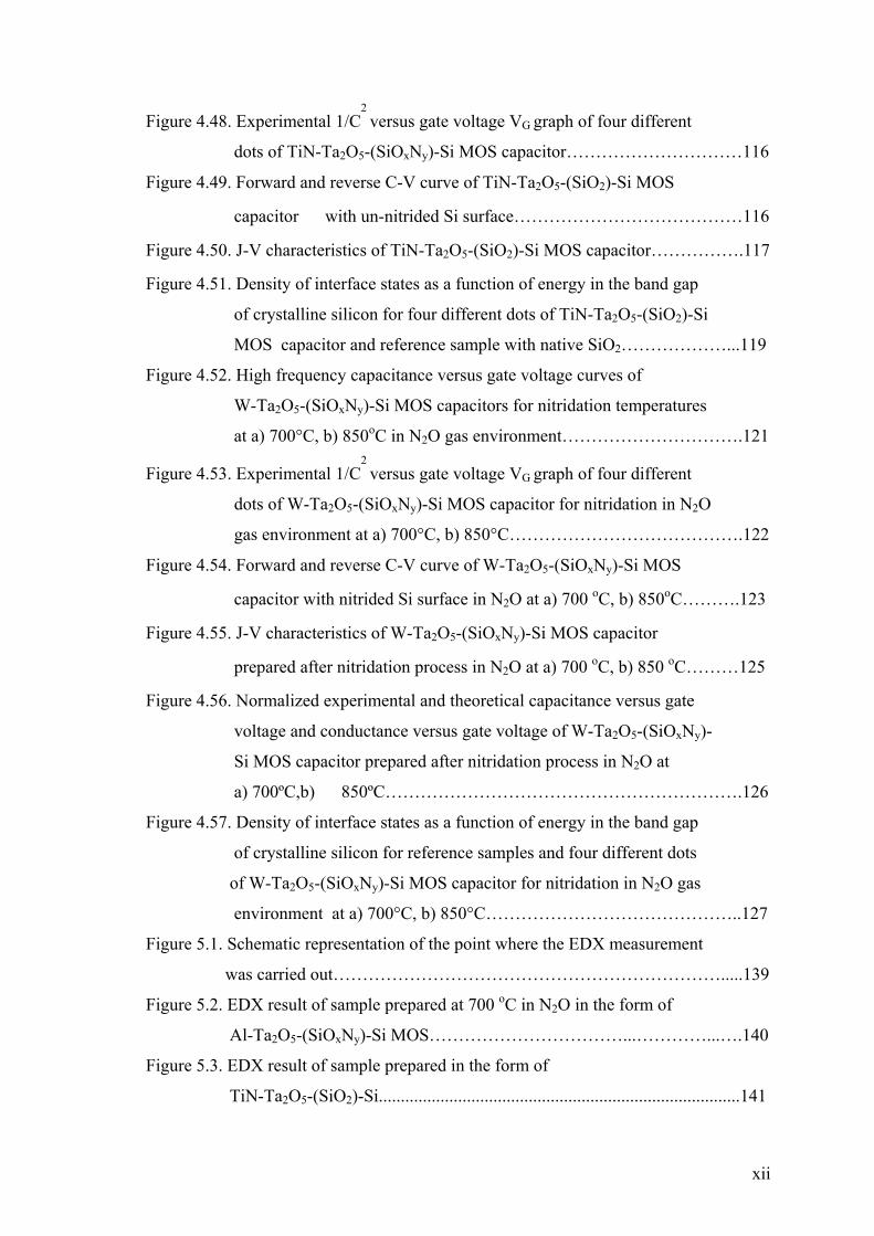
The electronics industry has grown rapidly in the past four decades. In the early
1960’s, on a piece of semiconductor putting more than one transistor was thought as the
cutting edge. Scientists have spent continuous effort to increase the number of devices
on the same chip area and the investigations contributed to the world science as cost
reduction in fabrication and improvement in device performance (Wolf 2002). The
increase of the number of transistor is best presented with Moore’s law, as illustrated in
Figure 1 with Intel® processors. Moore’s law states that the number of transistor
roughly doubles every 18 months resulting in higher performance with lower cost
(Moore 1965, WEB_2006). Moore’s law has been successfully observed for the past
forty years by the semiconductor industry, and still expected to be followed in the
coming years. The simple but profound statement of Moore’s law is the foundations of
semiconductor and computing industries. As it is indicated in Moore’s law, in order to
achieve 1 G-bit and higher capacity Dynamic Random Access Memories (DRAMs), the
number of capacitors inside a chip must be increased resulting in scaling down of
memory cell which causes several different problems with the conventionally used gate
metal and insulators.
Figure 1.1. Illustration of Moore’s law
(WEB_2006)
2
One of the most crucial elements that allow the successful scaling is certainly
the native oxide SiO2. It is used as a component in Metal- Oxide-Semiconductor (MOS)
capacitors of DRAM’s, and has served as a high quality electrical insulator for
integrated circuit (IC) applications for more than 40 years. SiO2 passivates Si surface
with a low surface-state density which is about 2-3x10¹⁰(eV-cm2)-1. Besides its
passivating properties, SiO2 acts as a barrier against the diffusion of impurities into the
silicon underneath and insulates the gate from the silicon (Nicollian and Brews 1982).
SiO2 is thermally very stable up to 1000°C which is required for the MOSFET
fabrication. In fact, the major driving of the microelectronics revolution is the
outstanding properties of SiO2, which include high resistivity, excellent dielectric
strength, a large band gap, a high melting point, and a native, low defect density
interface with Si.
In early fabrication technologies, silicon dioxide was frequently used as a mask
for ion implantation and than it is usually used for its dielectric properties (Campbell
2001). Since it was the only dielectric material used for the fabrication of integrated
circuits it has been studied in detail by many researchers (Nicollian and Brews 1982). In
order to achieve devices with best electronic quality, SiO2 is formed by using various
methods such as rapid thermal annealing (Paskaleva et al. 1995) and rapid thermal
nitridation (Moslehi et al. 1985). The surface states of silicon-silicon dioxide interface
have been extensively investigated by several techniques including measurement of the
energy distribution of surface trap states using the high-frequency (Terman 1962) and
quasistatic (Berglund 1966, Kuhn 1970) capacitance methods, the conductance method
(Nicollian and Goetzberger 1967), and the Gray and Brown technique (Gray and Brown
1966, Brown and Gray 1968). In addition, deep-level transient spectroscopy (DLTS)
(Schulz and Johnson 1977, Tredwell and Viswanathan 1980, Nicollian and Brews
1982), 1/f noise measurement (Butler and Hsiang 1988) and charge pumping (CP)
measurement techniques (Militaru et al. 2005) have also been used to characterize
interface properties.
MOS capacitors are the easiest MOS devices and any further development in
these devices can easily be applied to the transistor technology. In a MOS transistor,
applying bias to the gate electrode results in an electric field across the transistor
structure. This electric field arranges the carrier concentration in the channel and
controls the flow of current from the source to drain. Scaling down the device size gives
rise to an increase in electric field and therefore the performance of the device could be

3
enhanced since large electric field increases the drain current, which results in faster
switching speeds and lower power dissipation. It provides the consumer with faster
circuit performance, reduced energy consumption with longer battery lifetime and
reduced cost integrated circuit. In order to meet the demands for improved IC’s
performance, the microelectronics revolution has continued and the scaling of minimum
feature sizes of devices has been the major force of this revolution. For the needs of
high density DRAMs, researchers have started to reduce the thickness of the
conventional SiO2 gate dielectrics from hundreds nm to few nm to maintain the high
derive current and gate capacitance. Moreover, scaling the thickness of SiO2 increases
the capacitive coupling of the gate to the substrate and decreases the device resistance.
Thus, higher doping concentration can be used in the substrate while maintaining a low
resistance. The increase in doping concentration increases the barrier height, therefore
provide isolation between source and drain when the device is turned off (Packan 1999).
On the other hand, the technical challenge for continuing device scaling down
and Moore’s law is the scalability of the oxide thickness of MOS devices below 30 nm
due to off-state leakage (leakage current). International Technology Roadmap for
Semiconductor (ITRS) provides reasonably detailed guide to device scaling
requirements to keep the industry on the Moore’s law curve alive. Now, according to
the 2004 ITRS an equivalent oxide thickness (EOT) less than 0.8 nm is needed in the
near feature to allow the continuity of Moore’s law (ITRS 2004). However, in the
research carried out on SiO2 film thinner than 1.5 nm, large leakage current higher than
1 Acm-2 have been observed (Gou and Ma, 1998). Moreover, Muller et al. studied SiO2
with thickness ranging from 7 Ao to 15 Ao on Si by using electron energy loss
spectroscopy (EELS) and they could obtained the band gap of the oxide only for two
monolayer of SiO2 (Muller et al. 1999). This observation will set a physical limit to
SiO2 around 7-8 Ao since the thickness of each SiO2 monolayer is about 3,5- 4 Ao. On
the other hand, Timp et al. observed reduced drain current which degraded the device
performance in small transistor with less than 1.3 nm SiO2 thicknesses (Timp et al.
1997). It can be inferred from the frame of scaling device size that, drain current
increases with decreasing oxide thickness. Below such thickness values the tunneling
current increases exponentially with decreasing oxide thickness due to quantum
mechanical tunneling. As a result, gate leakage current continuously increases.
Although Moore’s law could be satisfied at some point, SiO2 does not possess its
inherited physical characteristics beyond such small thickness.

4
Since SiO2 with reduced thickness causes high leakage currents, increase in
power consumption, intrinsic device reliability, and circuit instabilities, researchers have
suggested using a high-permittivity (high-k) gate insulator with similar properties as
SiO2. Because of its high-k, such material will allow the scientist to use physically
thicker oxide in order to obtain the same capacitance value as that of conventional SiO2.
This will provide low leakage current with less probability of electrons and holes
tunneling trough the dielectric. In order to be used as gate dielectric, the material should
meet a set of criteria such as; dielectric constant higher than that of silicon dioxides
(k=3.9), thermodynamic stability on silicon, amorphous structure after device
integration, low conduction for low leakage (tunneling current less than 10mA/cm2),
low power consumption, high carrier mobility at the dielectric/Si interface, low
interface state density (Dit) ( ~1010 cm-2 eV-1), high breakdown strength acceptable
reliability and large band gap.
Dielectric constant higher than that of SiO2 is needed, to obtain the same oxide
capacitance as SiO2. Second important requirement is the thermodynamic stability of
high-k dielectric with Si surface. If the high-k material thermodynamically unstable on
SiO2, it will react with underlying Si substrate to form an interfacial layer which might
degrade the oxide capacitance and interface properties. On the other hand to minimize
the reaction of high-k dielectric with Si, high barrier height is needed. High band gap
and band offset are also among the requirement since they prevent the free flow from
substrate to metal electrode or vice versa. This will eliminate high leakage current and
breakdown problem. Furthermore, the high-k dielectric layer should be amorphous after
device integration since crystalline structure can results in non uniform oxide layer and
leakage path generation which finally results in higher leakage current.
Finally, the replacement of SiO2 native oxide with high dielectric constant
material has become one of the most important issues of microelectronic industry.
Considerable researches have been done on material systems such as Al2O3, Ta2O5,
TiO2, La2O3, Y2O3, Hf and Zr metal oxides and their silicates (Jeon et al. 2003, Groner
et al. 2002, Dimitrova and Atanassova 1998a, Cambell et al. 1997, Miranda et al. 2005,
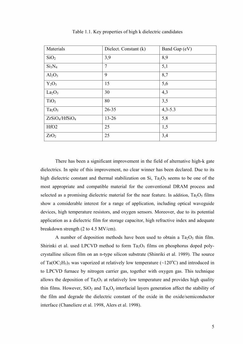
Callegari et al. 2001, Wang et al. 2003, Rhee et al. 2001). Table 1.1 shows the key
properties of high k dielectric candidates (Han 2003).
5
Table 1.1. Key properties of high k dielectric candidates
There has been a significant improvement in the field of alternative high-k gate
dielectrics. In spite of this improvement, no clear winner has been declared. Due to its
high dielectric constant and thermal stabilization on Si, Ta2O5 seems to be one of the
most appropriate and compatible material for the conventional DRAM process and
selected as a promising dielectric material for the near feature. In addition, Ta2O5 films
show a considerable interest for a range of application, including optical waveguide
devices, high temperature resistors, and oxygen sensors. Moreover, due to its potential
application as a dielectric film for storage capacitor, high refractive index and adequate
breakdown strength (2 to 4.5 MV/cm).
A number of deposition methods have been used to obtain a Ta2O5 thin film.
Shirinki et al. used LPCVD method to form Ta2O5 films on phosphorus doped poly-
crystalline silicon film on an n-type silicon substrate (Shinriki et al. 1989). The source
of Ta(OC2H5)5 was vaporized at relatively low temperature (~120oC) and introduced in
to LPCVD furnace by nitrogen carrier gas, together with oxygen gas. This technique
allows the deposition of Ta2O5 at relatively low temperature and provides high quality
thin films. However, SiO2 and TaxOy interfacial layers generation affect the stability of
the film and degrade the dielectric constant of the oxide in the oxide/semiconductor
interface (Chaneliere et al. 1998, Alers et al. 1998).
Materials Dielect. Constant (k) Band Gap (eV)
SiO2 3,9 8,9
Si3N4 7 5,1
Al2O3 9 8,7
Y2O3 15 5,6
La2O3 30 4,3
TiO2 80 3,5
Ta2O5 26-35 4,3-5.3
ZrSiO4/HfSiO4 13-26 5,8
HfO2 25 1,5
ZrO2 25 3,4

6
One of the simple deposition methods is oxidation process of Ta2O5 thin film on
a Si substrate by using the following steps. First, Ta films were deposited on a Si
substrate by RF sputtering from Ta target in an Ar atmosphere. Then, Ta films were
oxidized in dry O2 in a standard oxidation furnace (Atanassova 1999). This method has
a few drawbacks such as migration of silicon atoms from the substrate into the bulk of
the oxide and high interface trap density and formation of SiO2 interfacial layer.
Another commonly used deposition method of Ta2O5 oxide layer is RF
sputtering method. In RF sputtering, Ta2O5 thin films was deposited by reactive
sputtering of tantalum or tantalum oxide target at low pressure using an Ar/O2 gas
mixture as the sputtering gas (Dimitrova and Atanassova 1998b). Deposition of Ta2O5
on silicon substrate has been achieved in two ways: the first one is direct sputtering
from the Ta2O5 target and the second one is the reactive sputtering from Ta target in
oxygen atmosphere. The major benefit of this method is that it can be performed at
relatively low temperatures (in the range 150-400 oC). However, stoichiometry of the
oxide layer obtained with this method is rather difficult to control, and the films
generally present low density and often shows numerous pinholes. Inspite of these
drawbacks, as the sputtering can be suitably controlled, it may potentially offer
considerable material flexibility (Chaneliere et al. 1998).
Furthermore, Ta2O5 films were also obtained by sol-gel method (Lee et al.
1992). In this method Ta2O5 films were deposited by a spin-coating process. Tantalum
oxide coating solutions were prepared by hydrolysis of tantalum ethoxide in absolute
ethanol. The tantalum ethoxide was dissolved in ethanol. After the solution had been
stirred, it was diluted with ethanol and a small amount of water mixture. The mixed
solution was catalyzed with glacial acetic acid and stirred for 18 h to form the sol-
solution for the preparation of the Ta2O5 films. This solution was then dropped onto the
substrate surface (Yildirim et al. 2005). Although this method provides low temperature
processing, simple and compact equipment and high homogeneity of the deposited
films, the layers are mostly porous and contains large amount of CH based species. In
addition, other methods such as anodic oxidation, ion assisted deposition, electron-beam
evaporation, plasma enhanced CVD (PECVD), electron-beam vapor deposition or a
combination various techniques have been developed in order to obtain Ta2O5 oxide
layer. Even if the deposition method good or bad, the process must be economical and
should provide beneficial electronics properties and reliability for the device. However
despite the caution have been taken, XPS and high resolution transmission electron

7
microscopy (HRTEM) results undoubtedly reveal the formation of an ultra thin SiOx or
TaxOy interfacial layer at the Si- Ta2O5 interface for most of the deposition technique
while the formation of interfacial SiO2 is obviously an unavoidable process during
deposition of the oxide layer.
Structural characterization of Ta2O5 generally carried out using Auger electron
spectroscopy (AES), X-ray diffraction (XRD) and X-ray photoelectron spectroscopy
(XPS) measurement. Theoretical and experimental study of structural properties of
Ta2O5 reveals that, depending on the growth condition, the film can either be
amorphous or crystalline (Kimura et al. 1983). Research have done on Ta2O5 thin film
obtained by sol-gel method reveals that the as deposited and annealed at 973 oC oxide
layers are amorphous whereas crystalline orthorhombic phase of Ta2O5 was obtained at
annealing temperature above 973 oC (Lee et al. 1992). On the other hand, XRD result
for thermally grown insulator layers and recent research for Ta2O5 obtained with
different deposition methods shows that the crystallization temperature is range from
873 oC to 973 oC and it depends on film thickness and amorphous structures of the oxide
(Dimitrova et al. 2000, Kimura et al. 1983). Crystalline phase of Ta2O5 presents two
structures, orthorhombic (β- Ta2O5) and the second one is hexagonal (δ- Ta2O5)
structure. The β- Ta2O5 have lattice constants a=511.748 bohrs, b=56.948 bohrs, and
c=514.728 bohrs. It has two formula units of Ta2O5 with three Ta-O near neighbor
distances of 3.492, 3.674, and 3.809 bohrs. The hexagonal structure also contains two
formula units of Ta2O5 and two Ta-O near neighbor distances of 3.587 and 3.652 bohrs.
Its lattice constants are a=513.697 bohrs and c=57.332 bohrs. Encouraging electrical
properties have been obtained for amorphous Ta2O5 thin film, whereas there are no
sufficient studies on crystalline one. It is undesirable feature since it introduces non-
uniformity in the range of grain size and results in leakage path generation it is not
suggested to be used.
Optical properties of Ta2O5 thin film have been investigated using elipsometry
and optical transmission measurement. Ta2O5 thin film has an increasing refractive
index with the increased film thickness (Atanassova and Spassov 1998, Yoon et al.
2004). It was found that, the value of refractive index for thermally grown Ta2O5 is neff
=2 for the lowest thickness value and it increase with the increasing thickness up to 100
nm. It then saturates and stays around 2.22 for thickness higher than 100 nm. Similar
experimental results were reported for the reactive index of Ta2O5 films prepared using
different deposition methods (Chen et al. 1997).
8
The optical band gap of Ta2O5 was determined from the optical transmission
measurement. The optical band gap was found to be3.75± 0.12 eV for Ta2O5 deposited
by sol-gel dip- and spin-coating deposition techniques (Tepehan et al. 1997). However,
it is reported to be 4.2 eV for films made by RF sputtering method (Babeva et al. 2005).
These results indicate that, the optical band gap also depends on the deposition
conditions and type of deposition methods.
The conduction mechanism and electrical properties, which attract the scientist
to use high-k dielectric for the replacement of native oxide SiO2 in the development of
transistor technology, of Ta2O5 thin films are obtained from characteristics of MOS
structure. For this purpose Capacitance-Voltage (C-V) (Sun and Chen 1996), Current-
Voltage (I-V) (Ma 1997) and Conductance-Voltage (Chakraborty et al. 2004)
spectroscopies have been used. Applying voltage between metal gate and substrate in a
MOS structure provides one to determine the quality of the oxide layer and the quality
of the oxide-semiconductor interface. In addition to that, C-V and I-V and G-V
spectroscopies are used to investigate the dielectric constant, flat band voltage,
hysteresis behavior of the capacitor, the electrically active defects, conduction
mechanism in oxide and leakage current characteristics and doping concentration.
The electrical properties of Ta2O5 thin film are strongly dependent on the
deposition techniques. It was found that the dielectric constant of Ta2O5 shows
thickness dependence (Atanassova and Spassov 1998). Dielectric constant increases
with the increasing thickness. As the deposition temperature or annealing temperature is
increased, the dielectric constant can also be increased. On the other hand, crystalline
Ta2O5 has a higher dielectric constant than the amorphous one. In MOS capacitors, the
insulator should have high breakdown strength in order to prevent the charge flow result
from high electric field. When the amorphous Ta2O5 film crystallizes the breakdown
voltage decreases despite its increased dielectric constant (Dimitrova and Atanassova
1998c). As a result, a rush of charge flow will result in and device is broken down.
Once this happens the properties of the insulator becomes unpredictable. Furthermore,
the crystalline phase of tantalum pentoxide shows an anisotropic character. Depending
upon the crystal orientation, the dielectric constant could vary over a wide range, which
finally gives rise to uncertainty in the capacitance per unit area when used to make
MOS capacitors. Therefore, it could be possible that the dielectric constant of Ta2O5
layers used for submicron transistor structures could be different from one transistor to
another giving rise to a wide dispersion of device characteristics. Therefore, an
9
amorphous structure is preferred for microelectronics applications unless the crystal
orientation can be controlled in order to obtain the same characteristics from one
component to another.
Conduction mechanism of Ta2O5 layers have been studied extensively. Two
main conduction mechanisms were suggested to explain the current transport in Ta2O5
thin film as Schottky emission and Poole-Frenkel effect. Both mechanisms result from
the lowering of a Coulombic potential under an applied electric field. The Schottky
current is due to electrons which transit above the potential barrier at the surface of
metal or semiconductor and dominant at low electric fields below 2.2 MV/cm. On the
other hand, the Poole-Frenkel effect involves field enhanced electron emission from
Coulombic donor-like centers such as holes from acceptor centers and is dominant at
high fields above 2.2 MV/cm (Lee et al. 2001, Ezhilvalavan and Tseng 1999).
Leakage current density strongly influences the electrical properties of Ta2O5.
As the thickness of the oxide increases leakage current decreases. Leakage current of
Ta2O5 generally found to be in the range of 10-7-10-8A/cm2 under an applied electric
field up to 3MV cm-1 (Chaneliere et al. 1998). Since the thickness of SiO2 is increased
with increasing of Ta2O5 thickness, for thicker oxide film (tox>150nm), SiO2 dominates
on leakage current (Atanassova and Spassov 1998). That is why the range of the leakage
current strongly depends on the deposition condition (temperature, pressure, precursor
used) and annealing treatments (annealing technique, gasses employed, duration,
presence of an interfacial layer).
It is undoubted, SiO2 greatly responsible for conduction mechanism. On the
other hand there are evidences about the electrically active defects which possibly affect
the conduction mechanism in the Ta2O5-Si system. These defects result in non ideal
effect for MOS capacitors. They are occurs due to the deposition method, type of
insulator and environmental condition.
There are two types of charge in the insulator/Si layer; interface trap charge and
oxide charge. The oxide charge can be collected in three groups as fixed oxide charge,
oxide trapped charge and mobile ionic charge. The total of the oxide charges is called as
effective charge, Qeff. The effective oxide charge is independent of gate bias, whereas
interface charge trap varies with gate bias. Generally in the conduction mechanism of
MOS structure Qeff and the density of interface states caused by structural defect and
lattice mismatch between Ta2O5-Si interfaces, which is represented by Dit, takes a great
responsibility. For SiO2 the Dit level generally found to be in the range of ~ 1010
10
(eVcm2)-1 and the lower of the Dit, the better conduction mechanism thus electrical
properties, can be obtained since the expected interface is the one which have the less
interface trap charge. However when it’s compared with SiO2, Ta2O5 has higher
interface state density which is in the range of ~1012 (eVcm2)-1 due to dangling bond or
lattice mismatch.
Although Ta2O5 film provides high dielectric constant, however it is
thermodynamically unstable on silicon substrate due to the formation TaxOy and
unavoidable SiO2 formation. It has relatively high Dit level with high leakage current.
Quasi-static capacitance measurement of Ta2O5 has not been successfully investigated
due to the high level of leakage current. In addition, Ta2O5 oxide layer in MOS
capacitors show high density of effective oxide charge and hysteresis behaviors as the
gate voltage is swept from negative to positive and back to negative voltages. Such
hysteresis behavior is the cause of mobile trapped charges present in the oxide. In order
to improve the bulk and silicon-oxide interface properties of MOS capacitors with high-
k insulating layers, several pre and post deposition processes have been applied in
production of high quality devices. Such processes are furnace oxidation in O2 (Spassov
et al. 2000), plasma oxidation (Atanassova et al. 2002b), prior rapid thermal nitridation
in NO2 and NH3 gas (Novkovski et al. 2005) and rapid thermal annealing (Atanassova
et al. 2003a). However, the best results were obtained for the samples exposed to rapid
thermal nitridation (RTN) treatment before the formation of Ta2O5 oxide layers.
Formation of silicon oxynitride (Si0xNy) layer on a silicon substrate prevents the
interfacial SiO2 film growth problem and enhances the properties of the Ta2O5-Si
interface (Novkovski et al. 2005). It is also desirable to have such an interfacial layer
instead of SiO2 layer, since it has higher dielectric constant than SiO2. Si0xNy layer
passivates silicon surface from the oxide layer and thus helps to maintain high channel
mobility and prevents the reaction between the oxide and silicon which results in the
generation of the interface states (Gusev et al. 1999). Moreover, it provides an increase
in band offset, which increases the barrier height and reduces the leakage current. It is
concluded that RTN of the Si surface before deposition of Ta2O5 is a beneficial method
for remarkable improvement of the parameters of the Ta2O5/Si system in terms of
dielectric constant, leakage currents and the density of interface states (Novkovski et al.
2005, Tay and Hu 2004, Chaneliere et al. 1998).
The use of high-k dielectric materials will allow a significant reduction in
equivalent oxide thickness of the gate oxide itself and provide good electrical

11
characteristics for the MOSFET technology. However scaling down the device size,
that is the gate oxide size; affect not only the inherited properties of the gate oxide but
also properties of the gate electrode. Therefore replacement of the conventional gate
oxide, SiO2, with a high-k material is not a long term solution since as the high-k
material size scaled down the effect of the gate electrode can not be negligible.
Historically, the material used in MOSFET’s include a heavily doped
polycrystalline silicon (poly-silicon) gate electrode, a silicon dioxide gate dielectric and
lightly doped silicon substrate. Poly-silicon offered excellent thermal stability and
implemented a self-aligned process. However, as the device is scaled down and the
source/drain junction depths get shallower, the thermal budget becomes limited and
may cause insufficient dopant activation. The large boron concentration gradient
between the heavily doped poly-silicon gate electrode, the undoped oxide and lightly
doped silicon channel causes boron to diffuse rapidly trough sub-20 oA oxide upon
thermal annealing and cause to higher concentration of boron in the channel region.
This change in channel doping concentration then results in a shift in threshold voltage
which affects the device performance in an unacceptable way (Schaeffer III 2004,
Brown et al. 2004). On the other hand, it has been shown that as the electric field
increase during the device scaling, polysilicon depletion effect becomes an important
issue (Lo, Buchanan and Taur 1994). This depletion effect results in discrepancy
between the oxide capacitance and measured capacitance. Since the depleted poly-Si
gate will be under inversion and adds another capacitance to the device and increases
the EOT. Therefore the finite series capacitance of the poly-silicon gate can no longer
be neglected since it has a significant impact on the device performance. At that point,
replacing the polysilicon metal gate with appropriate one is come to mind. Thus the
depletion and penetration effect will be decreased and these will provide extra reduction
in gate oxide thickness. On the other hand, when it is compared with polysilicon, Debye
length of metals is shorter and thus it has higher carrier concentration and more
effective at screening charge. Moreover metal electrodes prevent the band banding and
this assists the device performance (Schaeffer III 2004). But in order to be used as a
metal gate, the new material should meet some requirement for the replacement of poly-
Si gate metal “(Sjöblom, Westlinder and Olsson, 2005), (Westlinder et al. 2004, Lugan
et al. 2002) such as stable in contact with gate dielectric, proper work function and high
reliability, metal work function should coincide with the valance band edge and
12
conductance band edge of Si, low charge density at metal gate/dielectric stack,
thermodynamic and chemical compatibility with gate dielectric and process integration.
The most effective requirements for the gate material are the work function and
interface thermal stability. Therefore requirements for a silicon compatible gate
electrode are stringent. The work function of the gate material, defined as the energy
needed to remove an electron from the Fermi level to the vacuum level, has to be within
a certain range. The currently required work function for p MOS capacitor is 4.25~5.25
eV (Lander et al. 2002) which is around valence band edge of Si (and around
conduction band for n-MOS capacitor). Therefore the random dopant placement
induced threshold (Vth) fluctuation and degradation in channel mobility would be
minimized and the device can come to thermal equilibrium condition without
deformation.
Depending on the work function, the suitable metals were used in an
appropriate condition. There have been some efforts to use a single metal gate electrode
with mid-gap workfunction to simplify the fabrication process. Since the nitridation
process improves the interface and the oxide properties, metal-nitride layers also take
great attention as a technologically important class of materials due to their mechanical
properties as well as chemical stability. Alternative solution was carried out by using
multilayer which reduce the gate resistance and improve the matching behavior
(Nguyen et al. 2005). In this way the work function can be tuned by adding the second
layer.
Presently, several metal gates candidates have been investigated which satisfy
the requirements such as TiN, W, Al, Mo, InSb, Ti/W, TiN/W, Ta, Au, TaN, TaSiN,
Ru, and TiAlN (Lugan et al. 2002, Lander et al. 2002, Khaleque 1995, Nguyen et al.
2005, Yun et al. 2005, Zier et al. 2004). Figure1.2 shows the distribution of the metals
over band edge of Si. These studies are motivated by the fact that it is necessary to form
a protective layer against oxidation and penetration of contaminants during high
temperature treatments after the oxide deposition.
13
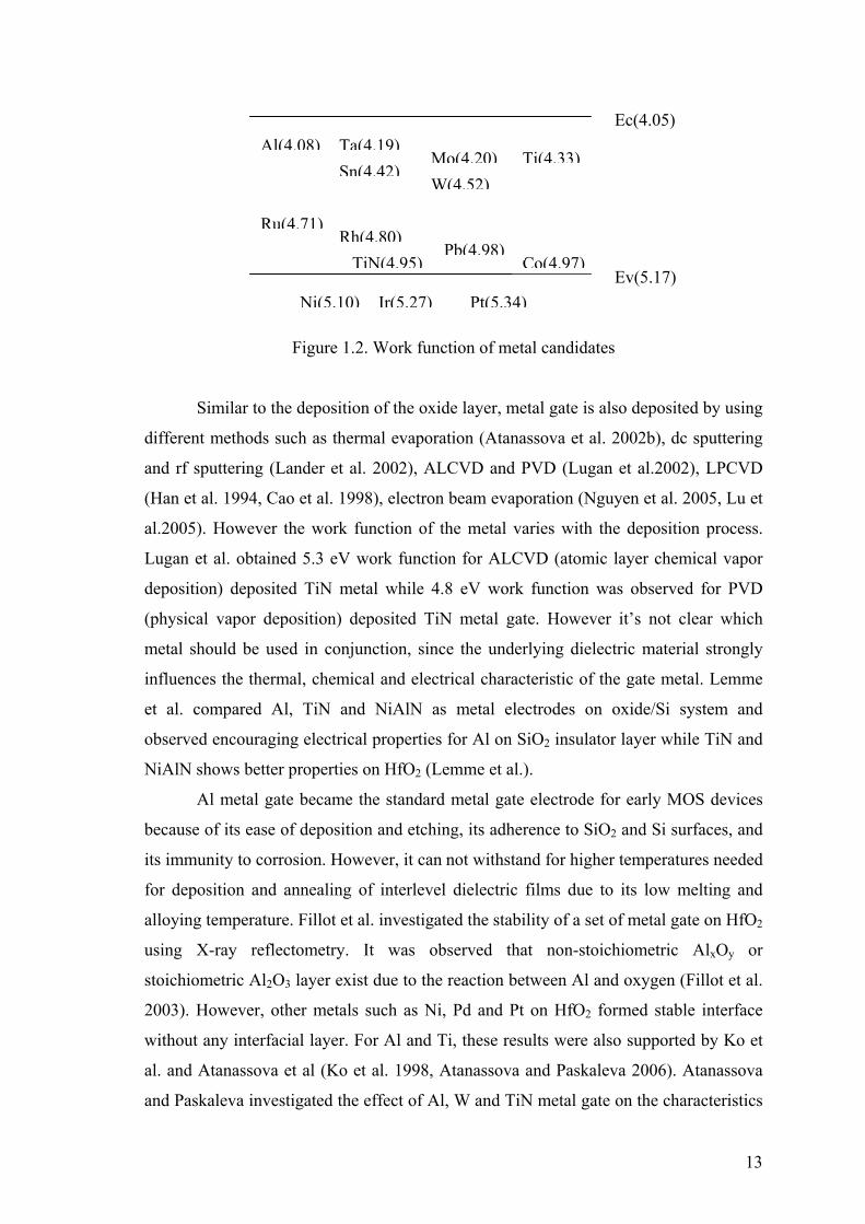
Figure 1.2. Work function of metal candidates
Similar to the deposition of the oxide layer, metal gate is also deposited by using
different methods such as thermal evaporation (Atanassova et al. 2002b), dc sputtering
and rf sputtering (Lander et al. 2002), ALCVD and PVD (Lugan et al.2002), LPCVD
(Han et al. 1994, Cao et al. 1998), electron beam evaporation (Nguyen et al. 2005, Lu et
al.2005). However the work function of the metal varies with the deposition process.
Lugan et al. obtained 5.3 eV work function for ALCVD (atomic layer chemical vapor
deposition) deposited TiN metal while 4.8 eV work function was observed for PVD
(physical vapor deposition) deposited TiN metal gate. However it’s not clear which
metal should be used in conjunction, since the underlying dielectric material strongly
influences the thermal, chemical and electrical characteristic of the gate metal. Lemme
et al. compared Al, TiN and NiAlN as metal electrodes on oxide/Si system and
observed encouraging electrical properties for Al on SiO2 insulator layer while TiN and
NiAlN shows better properties on HfO2 (Lemme et al.).
Al metal gate became the standard metal gate electrode for early MOS devices
because of its ease of deposition and etching, its adherence to SiO2 and Si surfaces, and
its immunity to corrosion. However, it can not withstand for higher temperatures needed
for deposition and annealing of interlevel dielectric films due to its low melting and
alloying temperature. Fillot et al. investigated the stability of a set of metal gate on HfO2
using X-ray reflectometry. It was observed that non-stoichiometric AlxOy or
stoichiometric Al2O3 layer exist due to the reaction between Al and oxygen (Fillot et al.
2003). However, other metals such as Ni, Pd and Pt on HfO2 formed stable interface
without any interfacial layer. For Al and Ti, these results were also supported by Ko et
al. and Atanassova et al (Ko et al. 1998, Atanassova and Paskaleva 2006). Atanassova
and Paskaleva investigated the effect of Al, W and TiN metal gate on the characteristics
Ev(5.17)
Ec(4.05) Al(4.08) Ta(4.19)
Mo(4.20) Ti(4.33)
Ru(4.71)Rh(4.80)
Co(4.97)Pb(4.98)
Ni(5.10) Ir(5.27) Pt(5.34)
TiN(4.95)
W(4.52)Sn(4.42)
14
of Ta2O5 gate oxide in terms of leakage current, breakdown field and dielectric constant
(Atanassova and Paskaleva 2006). While they observed interaction between the gate
metal and oxide for Al and TiN metal which degraded the characteristics of Ta2O5, no
reaction between W and Ta2O5 were observed. Moreover they observed improved
leakage current and dielectric constant for the capacitor with W metal gate.
Although TiN metal gate is compatible with low temperature process it shows
reaction with the underlying gate oxide as the temperature increased. Kwon et al.
formed TiN film on Ta2O5 film obtained by LPCVD (Kwon et al. 1996). They studied
the thermal degradation of Ta2O5 thin film by using XPS. They observed that, TiN
metal electrode oxidize for as deposited film and for capacitor exposed to high
temperature process (450-850 oC) with borophosphorus silicate glass (BPSG) reflow
process, the oxidation rate of TiN film increase. The effect of this oxidation in Ta2O5
observed to cause deterioration and increase in leakage current. On the other hand,
Lander et al. reported that the work function of the metal gate electrode has been
adjusted by the incorporation of nitrogen at the metal-oxide interface. They observed
that the diffused concentration of nitrogen increases with annealing temperature (Lander
et al. 2002). Nitrogen diffusion allows high concentration of mobile nitrogen, which
greatly influences the effective oxide charge and interface trap charge density in MOS
capacitor.
Even though there are several studies reported in the literature for the
investigation of the metal gate on high-k oxide layers, there is no conclusive reported
yet. Better candidate for replacement of poly-silicon gate in MOS capacitors with high-
k oxide layers require more detailed investigation.
1.1 Thesis Objective
The objective of this thesis is to investigate the effects of prior nitridation of
silicon surface and different metal gates on the electronic properties of high-k Ta2O5
oxide layers and silicon-high-k oxide interface properties. For this reason, a prior
nitridation process of silicon surface before formation of Ta2O5 insulating layers were
applied using N2O and NH3 gas ambients. Substrate temperature was changed between
700 C and 850 C during the nitridation processes. Then, formation of Ta2O5 oxide layers
were deposited using RF magnetron sputtering of Ta target in Ar and O2 gas. Finally, Al
15
metal contacts were evaporated on the high-k Ta2O5 oxide. In order to compare the
effects of prior nitridation process under two different gas ambients, two different
reference samples were also investigated. The first reference sample has the structure of
Al-SiO2-Si MOS capacitor and the second one was Al-Ta2O5-Si MOS capacitor without
any nitridation process of silicon surface. The high frequency C-V characteristics, G-V,
hysteresis C-V, and leakage current measurements were simultaneously performed on
several dots from each substrate. By using the theoretical C-V and high frequency
experimental C-V curves, effective dielectric constant, doping concentration of Si
substrate, flat band voltage shift, effective oxide charge density and finally interface trap
density were calculated for the samples. Then the results were compared with those of
reference samples. The improvements in the oxide and interface properties with the
nitridation process were indicated.
The second objective of this thesis was to investigate the effect of metal gate,
which can potentially change the properties of metal gate-oxide interface and finally
affects the characteristics of MOS capacitors. Different metal gates such as Al, TiN and
W were used as top electrode with Ta2O5 high-k oxide layer underneath. The effect of
different metal gates with the same oxide layer underneath was compared using the
results of high frequency C-V measurements, hysteresis C-V, G-V, and leakage current
measurements. Promising gate metal to replace the poly silicon gate contact was
determined from the analysis of the results.
16
CHAPTER 2
EXPERIMENTAL METHODS
2.1. Sample Preparation
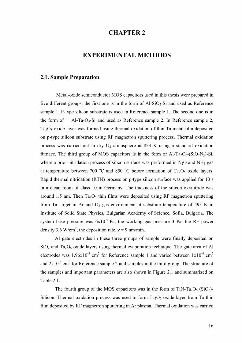
Metal-oxide semiconductor MOS capacitors used in this thesis were prepared in
five different groups, the first one is in the form of Al-SiO2-Si and used as Reference
sample 1. P-type silicon substrate is used in Reference sample 1. The second one is in
the form of Al-Ta2O5-Si and used as Reference sample 2. In Reference sample 2,
Ta2O5 oxide layer was formed using thermal oxidation of thin Ta metal film deposited
on p-type silicon substrate using RF magnetron sputtering process. Thermal oxidation
process was carried out in dry O2 atmosphere at 823 K using a standard oxidation
furnace. The third group of MOS capacitors is in the form of Al-Ta2O5-(SiOxNy)-Si,
where a prior nitridation process of silicon surface was performed in N2O and NH3 gas
at temperature between 700 oC and 850 oC before formation of Ta2O5 oxide layers.
Rapid thermal nitridation (RTN) process on p-type silicon surface was applied for 10 s
in a clean room of class 10 in Germany. The thickness of the silicon oxynitride was
around 1.5 nm. Then Ta2O5 thin films were deposited using RF magnetron sputtering
from Ta target in Ar and O2 gas environment at substrate temperature of 493 K in
Institute of Solid State Physics, Bulgarian Academy of Science, Sofia, Bulgaria. The
system base pressure was 6x10⁻⁴ Pa, the working gas pressure 3 Pa, the RF power
density 3.6 W/cm2, the deposition rate, ν = 9 nm/min.
Al gate electrodes in these three groups of sample were finally deposited on
SiO2 and Ta2O5 oxide layers using thermal evaporation technique. The gate area of Al
electrodes was 1.96x10⁻³ cm2 for Reference sample 1 and varied between 1x10⁻⁴ cm2
and 2x10⁻³ cm2 for Reference sample 2 and samples in the third group. The structure of
the samples and important parameters are also shown in Figure 2.1 and summarized on
Table 2.1.
The fourth group of the MOS capacitors was in the form of TiN-Ta2O5 (SiO2)-
Silicon. Thermal oxidation process was used to form Ta2O5 oxide layer from Ta thin
film deposited by RF magnetron sputtering in Ar plasma. Thermal oxidation was carried
17
out in dry O2 gas at 823 K. Finally, TiN gate metal was deposited on thermally grown
Ta2O5 oxide using RF magnetron sputtering technique. During the thermal oxidation of
Ta metal films there exists very thin inevitable native oxide SiO2 between Ta2O5 high-k
oxide layer and p-type silicon substrate. For this group of samples, a post metallization
annealing in H2 gas was carried out at 450 K for one hour.
The last group of MOS capacitors was prepared in the form of W-Ta2O5-
SiOxNy-Silicon. Similar to the third group samples, a prior nitridation process of p-type
silicon substrate was applied in N2O gas at 700 oC and 850 oC using RTN process in a
clean room of class 10. The thickness of the SiOxNy interfacial layer was around 1.5-2
nm. Tantalum films were deposited on Si by RF sputtering of Ta target in Ar
atmosphere after the chemical cleaning of the wafer. The system base pressure was
6x10⁻⁴ Pa, the working gas pressure 3 Pa, the RF power density 3.6 W/cm2, the
deposition rate, ν = 9.3 nm/min. During the Ta deposition the substrates were not
intentionally heated and presumably remained at a temperature close to the room one.
After that, Ta films were oxidized in dry O2 at atmospheric pressure at 873 K in a
standard oxidation furnace. The films thickness were measured as 22 nm by elipsometry
(λ = 632.8 nm). The oxidation was fallowed by rf sputtering of W targets to deposit W
metal gate on Ta2O5 oxide layers. No post metallization annealing was performed.
For all the samples, preparation processes, except RTN process, were carried out
by Prof. E. Atanassova at Institute of Solid State Physics, Bulgarian Academy of
Science in Sofia, Bulgaria.

18
Figure 2.1. Composition of metal-oxide-semiconductor MOS capacitors used in this
thesis
W
SiOxNy
Si
Ta2O5- 22 nm
Group 5 Al
SiOxNy
Si
Ta2O5- 20 nm
Group 3
TiN
SiO2
Si
Ta2O5- 15 nm
Group 4
Al
SiO2
Si
Ta2O5- 20 nm
Group 2
Al
SiO2- 20 nm
Si
Group 1
19
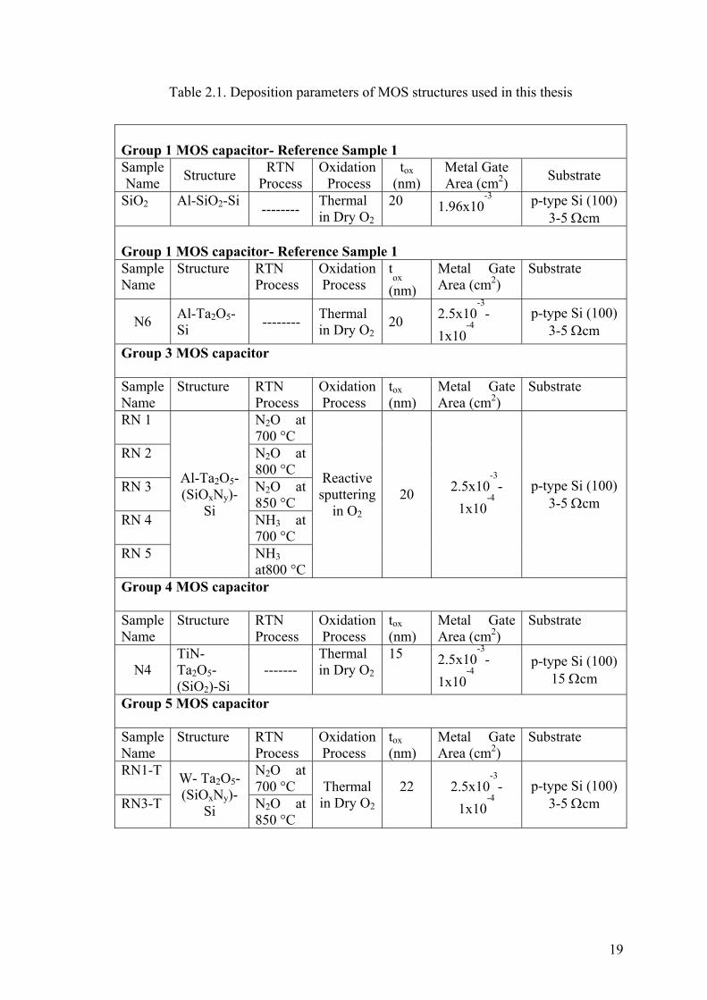
Table 2.1. Deposition parameters of MOS structures used in this thesis
Group 1 MOS capacitor- Reference Sample 1 Sample Name Structure RTN
Process Oxidation Process
tox (nm)
Metal Gate Area (cm2) Substrate
SiO2 Al-SiO2-Si -------- Thermal in Dry O2
20 1.96x10⁻³
p-type Si (100) 3-5 Ωcm
Group 1 MOS capacitor- Reference Sample 1 Sample Name
Structure RTN Process
Oxidation Process
tox
(nm) Metal Gate Area (cm2)
Substrate
N6 Al-Ta2O5-Si -------- Thermal
in Dry O2 20 2.5x10
-3-
1x10⁻⁴
p-type Si (100)
3-5 Ωcm Group 3 MOS capacitor Sample Name
Structure RTN Process
Oxidation Process
tox (nm) Metal Gate Area (cm2)
Substrate
RN 1 N2O at 700 °C
RN 2 N2O at 800 °C
RN 3 N2O at 850 °C
RN 4 NH3 at 700 °C
RN 5
Al-Ta2O5-(SiOxNy)-
Si
NH3 at800 °C
Reactive sputtering
in O2
20 2.5x10⁻³
-1x10
-4
p-type Si (100) 3-5 Ωcm
Group 4 MOS capacitor Sample Name
Structure RTN Process
Oxidation Process
tox (nm) Metal Gate Area (cm2)
Substrate
N4 TiN- Ta2O5-(SiO2)-Si
------- Thermal in Dry O2
15 2.5x10⁻³
-1x10
-4
p-type Si (100) 15 Ωcm
Group 5 MOS capacitor Sample Name
Structure RTN Process
Oxidation Process
tox (nm) Metal Gate Area (cm2)
Substrate
RN1-T N2O at 700 °C
RN3-T
W- Ta2O5-(SiOxNy)-
Si N2O at 850 °C
Thermal in Dry O2
22
2.5x10⁻³
-1x10
-4
p-type Si (100) 3-5 Ωcm

20
2.2 Characterization Techniques
This part will be devoted to the characterization techniques where the
instrumentation and details of simultaneous Capacitance- Voltage (C-V) spectroscopy
will be given.
2.2.1 Capacitance-Voltage (C- V) Spectroscopy
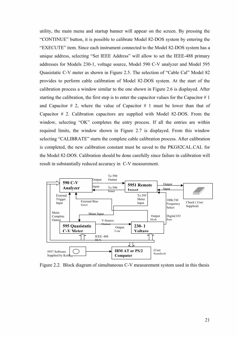
Model 82-DOS simultaneous C-V spectroscopy is a computer- controlled
system of instruments designed to make simultaneous quasistatic C-V and high
frequency (100 kHz and 1 MHz) C-V measurements on MOS capacitor. A diagram of
the system is shown in Figure 2.2. The system includes Model 590 C-V Analyzer in
order to supply high frequency voltage signal and measure capacitance and conductance
when making high frequency C-V measurement, and a Model 595 Quasistatic C-V
Meter for low frequency C-V and Q/t measurement. In addition, system also includes
Model 230-1 DC power supply, which is used to supply a DC voltage of up to ± 100 V
and a Model 5951 Remote Input Coupler for connecting the Model 590 and 595 inputs
to the device under test. Model 5951 contains tuned circuit which minimizes interaction
between low and high frequency measurement. Each instrument is connected to the
other by using BNC cables. In order to use the system, the instruments are connected to
the computer by using a Keithly IEEE- 488 BUS connection and a model 5957
Software program is used to control the experimental setup and to collect data.
Model 82- DOS system is programmed for Al metal gate and SiO2 gate oxide on
Si substrate. For each MOS capacitor with different oxide layer or metal gate, “Material
Constants File”, where the necessary constant and device parameters are stored, should
be modified. For every entry to MATERIAL.CON file, even no change have been
done, the file should be saved before exiting the file otherwise the program could not
locate it at run time. Opening MATERIAL.CON file provides the default menu which
as shown in Figure 2.3. For each MOS devices necessary changes were made and the
file was saved before exiting the file.
Another important issue is the cable calibration. Since the cables are sensitive to
the temperature changes, they should be calibrated frequently. Cable calibration is
performed by CABLECAL.EXE utility as shown in Figure 2.4. After running this
21
utility, the main menu and startup banner will appear on the screen. By pressing the
“CONTINUE” button, it is possible to calibrate Model 82-DOS system by entering the
“EXECUTE” item. Since each instrument connected to the Model 82-DOS system has a
unique address, selecting “Set IEEE Address” will allow to set the IEEE-488 primary
addresses for Models 230-1, voltage source, Model 590 C-V analyzer and Model 595
Quasistatic C-V meter as shown in Figure 2.5. The selection of “Cable Cal” Model 82
provides to perform cable calibration of Model 82-DOS system. At the start of the
calibration process a window similar to the one shown in Figure 2.6 is displayed. After
starting the calibration, the first step is to enter the capacitor values for the Capacitor # 1
and Capacitor # 2, where the value of Capacitor # 1 must be lower than that of
Capacitor # 2. Calibration capacitors are supplied with Model 82-DOS. From the
window, selecting “OK” completes the entry process. If all the entries are within
required limits, the window shown in Figure 2.7 is displayed. From this window
selecting “CALIBRATE” starts the complete cable calibration process. After calibration
is completed, the new calibration constant must be saved to the PKG82CAL.CAL for
the Model 82-DOS. Calibration should be done carefully since failure in calibration will
result in substantially reduced accuracy in C-V measurement.
Figure 2.2. Block diagram of simultaneous C-V measurement system used in this thesis
5957 Software Supplied by Keithly
To 590 Output
590 C-V Analyzer 5951 Remote
Input
595 Quasistatic C-V Meter
230- 1 Voltage
IBM AT or PS/2 Computer
Chuck ( User Supplied)
External Bias Input
To 595 Meter Input
V-Source Output
Output Input
100k/1M Frequency Select
Digital I/O Port
To 590 Input
Output
Input
External Trigger Input
Meter CompleteOutput
Meter Input Output High
Output Low
(User Supplied)
IEEE–488 BUS

22
FILE: MATERIAL.CON
DESCRIPTION: This file is used to initialize the physical constants associated with a
particular type of MIS device. This file contains physical constants for the following
device type at room temperature:
Silicon –Silicon Dioxide – Aluminum
insulator
sustrate material gate material
VARIABLE DESCRIPTION VALUE
KQ Charge of an electron (Coul) ! = 1.60219E-19
Kk Boltzmann’s constant (J/K) ! = 1.38066E-23
Kt Test temperature (K) ! = 293
KEox Permittivity of oxide (F/cm) ! = 3.40000E-13
KEs Permitivity of semiconductor (F/cm) ! = 1.04000E-12
KEg Energy gap of semiconductor (eV) ! = 1.12
KNi Intrinsic carrier concentration (1/cm^3) ! = 1.45000E+10
KPhim Metal work function (V) ! = 4.1
*KX Semiconductor electron affinity (V) ! = 4.15
(see note)
In modern integrated-circuit processing, heavily doped polysilicon is often used as the
gate material instead of aluminum. If this is the case, the work function constants are
computed as fallows (as per Sze’s book “Physics of Semiconductor Devices”).
p-type polysilicon gate
KPhim = Semiconductor electron affinity + Energy gap of semiconductor
n-type polysilicon gate
KPhim = Semiconductor electron affinity
Figure 2.3. Default values stored in material constant

23
Figure 2.4. Main menu and startup banner
Figure2.5. Set IEEE address window
Set IEEE Address(s)
Model 590 Address: Model 590 Address: (used for Model82 cal) Model 230 Address: (used for Model82 cal)
15
28
13
< OK> <CANCEL>
<CONTINUE>
Model–590 Cable Calibration Utility I /O Tech Version V0.00.002
Copyright (c) 1991 Keithly Instruments, Inc
24
Figure 2.6. Model 82 calibration source value entry window
Figure 2.7. Calibrate/ Send constants window
How do you wish to proceed?
<CALIBRATE> <SEND CONSTANTS> <CANCEL>
Model 82: 200 pF Range
47 pF 46.3864 pF 46.381 pF
< OK> <CANCEL>
46.385 pF
CAPACITOR # 1
Nominal 1 kHz 100 kHz 1 MHz
CAPACITOR # 2
Nominal 180 pF 182.732 pF 182.71 pF 182.77 pF
1 kHz 100 kHz 1 MHz

25
After all necessary calibrations and constants modification carried out, for the
characterization the sample is placed in a homemade Faraday cage which is made up of
aluminum metal. Faraday cage is an enclosure box designed to exclude the effect of
electromagnetic fields. The connection of the system to the sample is provided by a
homemade probe station with a micro manipulator. Gold wire is used as a probe wire in
order to have a good contact the device. To be able to use it as a probe wire, gold wire
was first sharpened by the electrolysis process then sanding process was applied to
obtain a precise contact area for the smaller gate areas. The contacts are placed on the
sample under the optical microscope.
In order to obtain an appropriate start and stop voltage necessary for obtaining
the device parameter, a diagnostic C-V measurement should be run from accumulation
to the inversion. From the main menu shown in Figure 2.8, option 3 allows us to reach
the sub menu for diagnostic C-V measurement as shown in figure 2.9. Before running a
sweep, the most important step is to set the start and stop voltages, step voltage and
delay time by selecting option 1 in Figure 2.9. Measurement parameters list is shown in
figure 2.10.
After setting the parameter list, it is possible to run a diagnostic C-V
measurement by selecting option 2 in Figure 2.9. After the measurement is completed,
the graph of the measurement can be seen by selecting option 3. A typical graph of C-V
measurement is shown in Figure 2.11. If the curve has the expected shape then the
device should be biased in accumulation and inversion to determine the oxide
capacitance, gate area, oxide thickness, minimum capacitance and optimum delay time
as well as series resistance by selecting option 4 and 5 of the menu shown in figure 2.9.
Once the device parameters are obtained, it is possible to run a real C-V
measurement by selecting option 4 of the menu shown in Figure 2.8. A sub menu for C-
V measurement is shown in Figure 2.12. Selecting “option 1” in Figure 2.12 provides
accessing the parameter list. In this menu the step voltage can be selected as small as
possible in order to obtain more data points for the accuracy of the analysis. Selecting
“option 2” in Figure 2.12 provides making C-V measurement manually. After the
measurement is completed option 4 in figure 2.12 is used to analyze the measurement
data as shown in Figure 2.13. This menu also provides graphing of the array data.
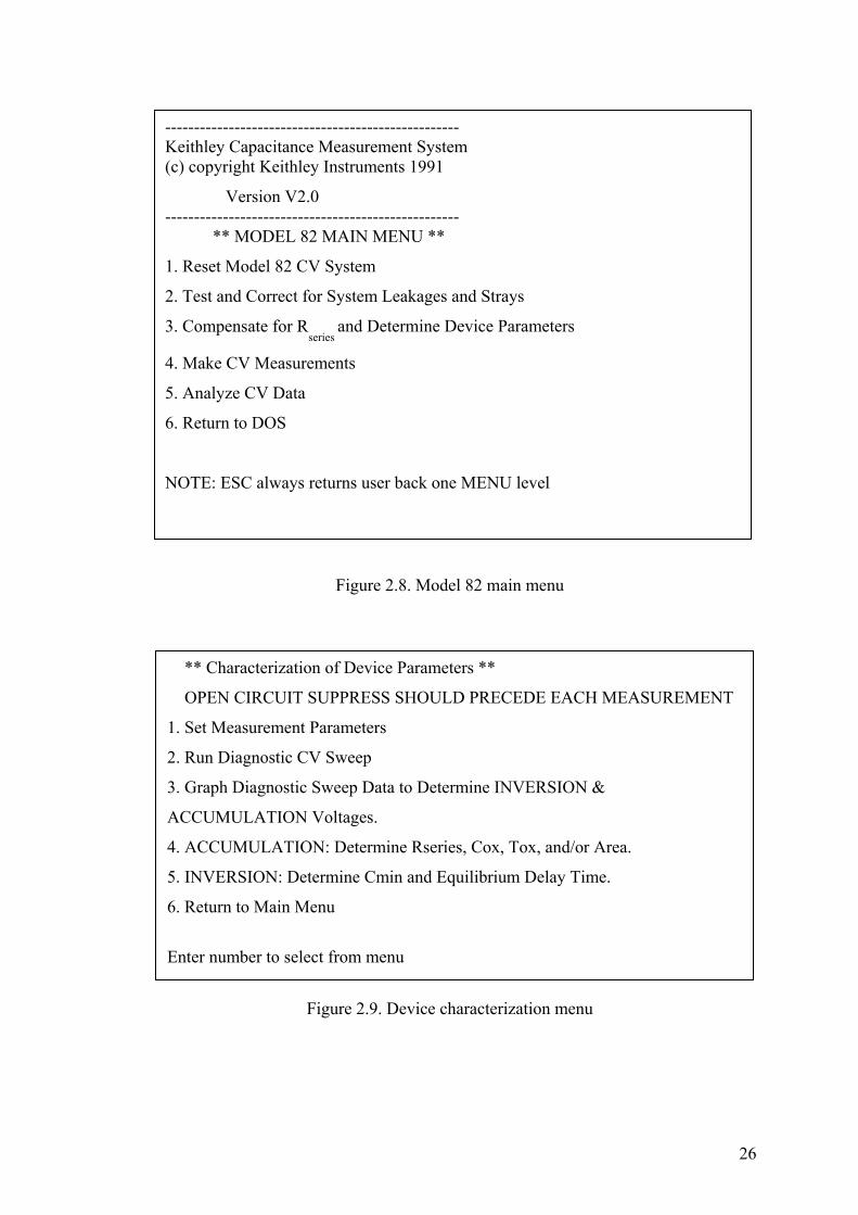
26
Figure 2.8. Model 82 main menu
Figure 2.9. Device characterization menu
--------------------------------------------------- Keithley Capacitance Measurement System (c) copyright Keithley Instruments 1991
Version V2.0 --------------------------------------------------- ** MODEL 82 MAIN MENU **
1. Reset Model 82 CV System
2. Test and Correct for System Leakages and Strays
3. Compensate for Rseries
and Determine Device Parameters
4. Make CV Measurements
5. Analyze CV Data
6. Return to DOS
NOTE: ESC always returns user back one MENU level
** Characterization of Device Parameters **
OPEN CIRCUIT SUPPRESS SHOULD PRECEDE EACH MEASUREMENT
1. Set Measurement Parameters
2. Run Diagnostic CV Sweep
3. Graph Diagnostic Sweep Data to Determine INVERSION &
ACCUMULATION Voltages.
4. ACCUMULATION: Determine Rseries, Cox, Tox, and/or Area.
5. INVERSION: Determine Cmin and Equilibrium Delay Time.
6. Return to Main Menu
Enter number to select from menu

27
Figure 2.10. Parameter selection menu
Figure 2.11. High and low frequency C-V graphic of MOS capacitor
** Measurement Parameter List ** Range: 2 Enter R1 for 200pF, R2 for 2nF
Freq : 2 Enter F1 for 100KHZ, F2 for 1MHZ
Model: 1 Enter M1 for parallel, M2 for series
Start V: 2.00 V. Enter An, -120 <= n <= 120
Stop V: -2.00 V. Enter On, -120 <= n <= 120
Bias V: 0.00 V. Enter Bn, -120 <= n <= 120
TDelay: 0.07 sec. Enter Tn, 0.07 <= n <= 199.99
Step V: 20 mV. Enter S10, S20, S50 or S100
CCap: 1 Enter C1 for leakage correction off, C2 for on
Filter: 2 Enter I1 for filter off, I2 for on
Number of samples = 93 Sweep will take = 0.4 minutes.
NOTE: 1) Keep start V and stop V within 40 volts of each other.
2) Keep number of samples within 4 and 1000 points with filter off.
3) Keep number of samples within 50 and 1000 points with filter on
Enter changes one changes at a time. Enter E when done, * for files.
Enter selection:
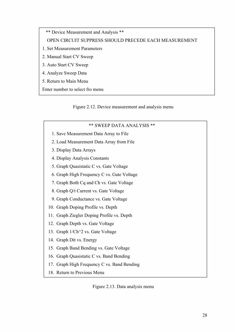
28
Figure 2.12. Device measurement and analysis menu
Figure 2.13. Data analysis menu
** Device Measurement and Analysis **
OPEN CIRCUIT SUPPRESS SHOULD PRECEDE EACH MEASUREMENT
1. Set Measurement Parameters
2. Manual Start CV Sweep
3. Auto Start CV Sweep
4. Analyze Sweep Data
5. Return to Main Menu
Enter number to select fro menu
** SWEEP DATA ANALYSIS **
1. Save Measurement Data Array to File
2. Load Measurement Data Array from File
3. Display Data Arrays
4. Display Analysis Constants
5. Graph Quasistatic C vs. Gate Voltage
6. Graph High Frequency C vs. Gate Voltage
7. Graph Both Cq and Ch vs. Gate Voltage
8. Graph Q/t Current vs. Gate Voltage
9. Graph Conductance vs. Gate Voltage
10. Graph Doping Profile vs. Depth
11. Graph Ziegler Doping Profile vs. Depth
12. Graph Depth vs. Gate Voltage
13. Graph 1/Ch^2 vs. Gate Voltage
14. Graph Dit vs. Energy
15. Graph Band Bending vs. Gate Voltage
16. Graph Quasistatic C vs. Band Bending
17. Graph High Frequency C vs. Band Bending
18. Return to Previous Menu

29
The “ANALYSIS” menu provides saving, loading and graphing of the reading
and graphics array data. It is also provides graphical and mathematical analysis of the
data array. In this menu, mathematical analysis of some parameters such as density of
interface trap, Dit, base on the data array of both high and low frequency C-V
measurement are carried out. MOS capacitors are charged by the displacement current
induced by the voltage ramp. In order to be able to measure low frequency C-V curve
the leakage current through the gate dielectric layer should be negligible compared to
displacement current. Although for thick gate oxide this could be obtained, very large
tunneling current from thin gate oxide makes the measurement invalid. Since the
samples that are used in this study are very thin, only Terman’s method is used for MOS
devices with Ta2O5 oxide layers instead of High-Low frequency C-V method to
calculate Dit.
The dielectric constant (k), equivalent oxide thickness (teqq) and flat band (VFB)
voltage were calculated by using high frequency C-V curve. The depletion capacitance
is used to estimate the Si substrate doping concentration (N). The flat band obtained
from the C-V curve was used to calculate effective oxide charge density (Neff).
Corrected conductance and leakage current were calculated from the row data of high
frequency C-V and conductance. Mobile charge trap obtained from the hysteresis shift,
the voltage shift between the reverse and forward bias C-V measurement. Theoretical
ideal C-V characteristics were calculated by using a computer program and equation
defined for MOS devices. The density of interface trap states were calculated from the
high frequency C-V curve by using Terman’s method.
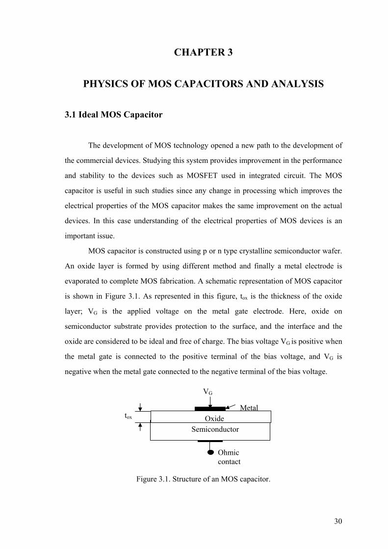
30
CHAPTER 3
PHYSICS OF MOS CAPACITORS AND ANALYSIS
3.1 Ideal MOS Capacitor
The development of MOS technology opened a new path to the development of
the commercial devices. Studying this system provides improvement in the performance
and stability to the devices such as MOSFET used in integrated circuit. The MOS
capacitor is useful in such studies since any change in processing which improves the
electrical properties of the MOS capacitor makes the same improvement on the actual
devices. In this case understanding of the electrical properties of MOS devices is an
important issue.
MOS capacitor is constructed using p or n type crystalline semiconductor wafer.
An oxide layer is formed by using different method and finally a metal electrode is
evaporated to complete MOS fabrication. A schematic representation of MOS capacitor
is shown in Figure 3.1. As represented in this figure, tox is the thickness of the oxide
layer; VG is the applied voltage on the metal gate electrode. Here, oxide on
semiconductor substrate provides protection to the surface, and the interface and the
oxide are considered to be ideal and free of charge. The bias voltage VG is positive when
the metal gate is connected to the positive terminal of the bias voltage, and VG is
negative when the metal gate connected to the negative terminal of the bias voltage.
Figure 3.1. Structure of an MOS capacitor.
VG
MetalOxide
Semiconductor
tox
Ohmic contact
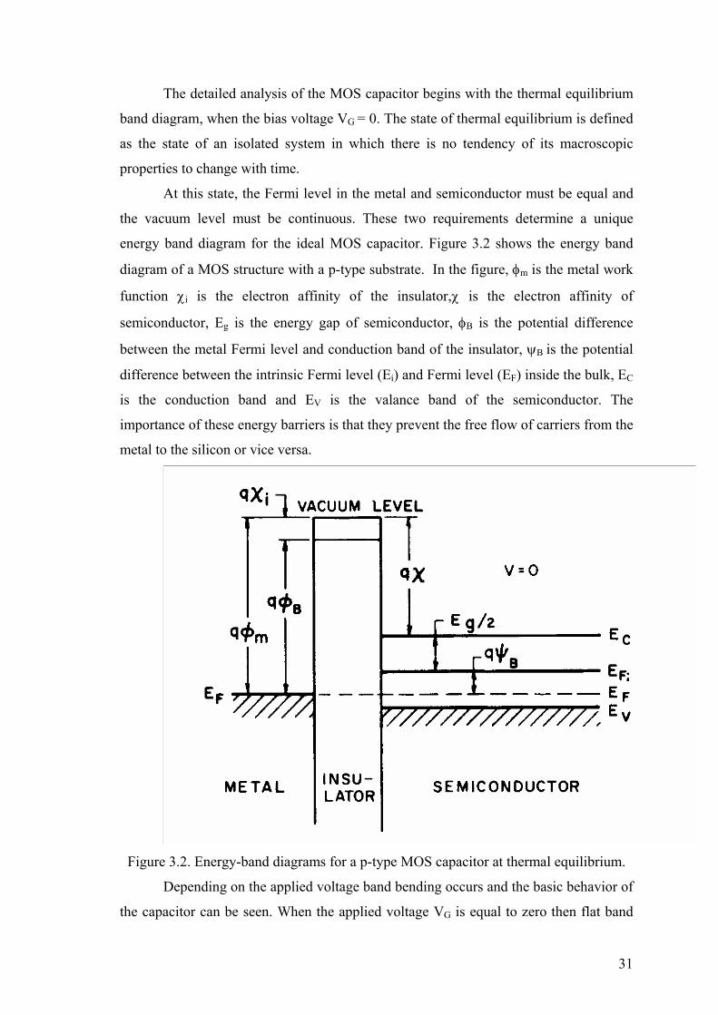
31
The detailed analysis of the MOS capacitor begins with the thermal equilibrium
band diagram, when the bias voltage VG = 0. The state of thermal equilibrium is defined
as the state of an isolated system in which there is no tendency of its macroscopic
properties to change with time.
At this state, the Fermi level in the metal and semiconductor must be equal and
the vacuum level must be continuous. These two requirements determine a unique
energy band diagram for the ideal MOS capacitor. Figure 3.2 shows the energy band
diagram of a MOS structure with a p-type substrate. In the figure, φm is the metal work
function χi is the electron affinity of the insulator,χ is the electron affinity of
semiconductor, Eg is the energy gap of semiconductor, φB is the potential difference
between the metal Fermi level and conduction band of the insulator, ψB is the potential
difference between the intrinsic Fermi level (Ei) and Fermi level (EF) inside the bulk, EC
is the conduction band and EV is the valance band of the semiconductor. The
importance of these energy barriers is that they prevent the free flow of carriers from the
metal to the silicon or vice versa.
Figure 3.2. Energy-band diagrams for a p-type MOS capacitor at thermal equilibrium.
Depending on the applied voltage band bending occurs and the basic behavior of
the capacitor can be seen. When the applied voltage VG is equal to zero then flat band
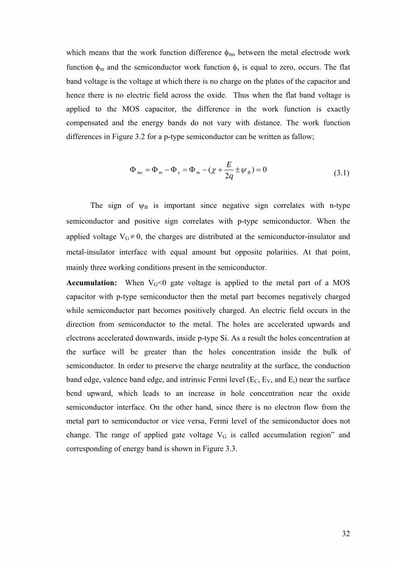
32
which means that the work function difference φms between the metal electrode work
function φm and the semiconductor work function φs is equal to zero, occurs. The flat
band voltage is the voltage at which there is no charge on the plates of the capacitor and
hence there is no electric field across the oxide. Thus when the flat band voltage is
applied to the MOS capacitor, the difference in the work function is exactly
compensated and the energy bands do not vary with distance. The work function
differences in Figure 3.2 for a p-type semiconductor can be written as fallow;
0)2
( =±+−Φ=Φ−Φ=Φ Bmsmms qE ψχ (3.1)
The sign of ψB is important since negative sign correlates with n-type
semiconductor and positive sign correlates with p-type semiconductor. When the
applied voltage VG≠ 0, the charges are distributed at the semiconductor-insulator and
metal-insulator interface with equal amount but opposite polarities. At that point,
mainly three working conditions present in the semiconductor.
Accumulation: When VG<0 gate voltage is applied to the metal part of a MOS
capacitor with p-type semiconductor then the metal part becomes negatively charged
while semiconductor part becomes positively charged. An electric field occurs in the
direction from semiconductor to the metal. The holes are accelerated upwards and
electrons accelerated downwards, inside p-type Si. As a result the holes concentration at
the surface will be greater than the holes concentration inside the bulk of
semiconductor. In order to preserve the charge neutrality at the surface, the conduction
band edge, valence band edge, and intrinsic Fermi level (EC, EV, and Ei) near the surface
bend upward, which leads to an increase in hole concentration near the oxide
semiconductor interface. On the other hand, since there is no electron flow from the
metal part to semiconductor or vice versa, Fermi level of the semiconductor does not
change. The range of applied gate voltage VG is called accumulation region” and
corresponding of energy band is shown in Figure 3.3.
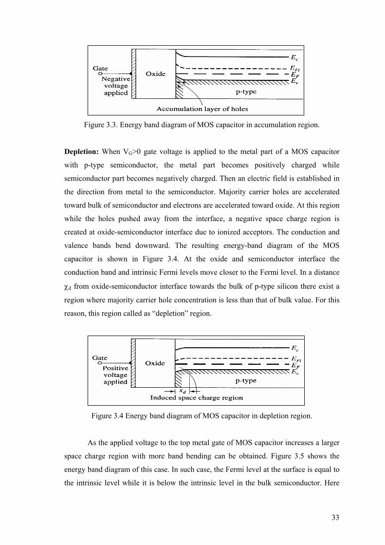
33
Figure 3.3. Energy band diagram of MOS capacitor in accumulation region.
Depletion: When VG>0 gate voltage is applied to the metal part of a MOS capacitor
with p-type semiconductor, the metal part becomes positively charged while
semiconductor part becomes negatively charged. Then an electric field is established in
the direction from metal to the semiconductor. Majority carrier holes are accelerated
toward bulk of semiconductor and electrons are accelerated toward oxide. At this region
while the holes pushed away from the interface, a negative space charge region is
created at oxide-semiconductor interface due to ionized acceptors. The conduction and
valence bands bend downward. The resulting energy-band diagram of the MOS
capacitor is shown in Figure 3.4. At the oxide and semiconductor interface the
conduction band and intrinsic Fermi levels move closer to the Fermi level. In a distance
χd from oxide-semiconductor interface towards the bulk of p-type silicon there exist a
region where majority carrier hole concentration is less than that of bulk value. For this
reason, this region called as “depletion” region.
Figure 3.4 Energy band diagram of MOS capacitor in depletion region.
As the applied voltage to the top metal gate of MOS capacitor increases a larger
space charge region with more band bending can be obtained. Figure 3.5 shows the
energy band diagram of this case. In such case, the Fermi level at the surface is equal to
the intrinsic level while it is below the intrinsic level in the bulk semiconductor. Here
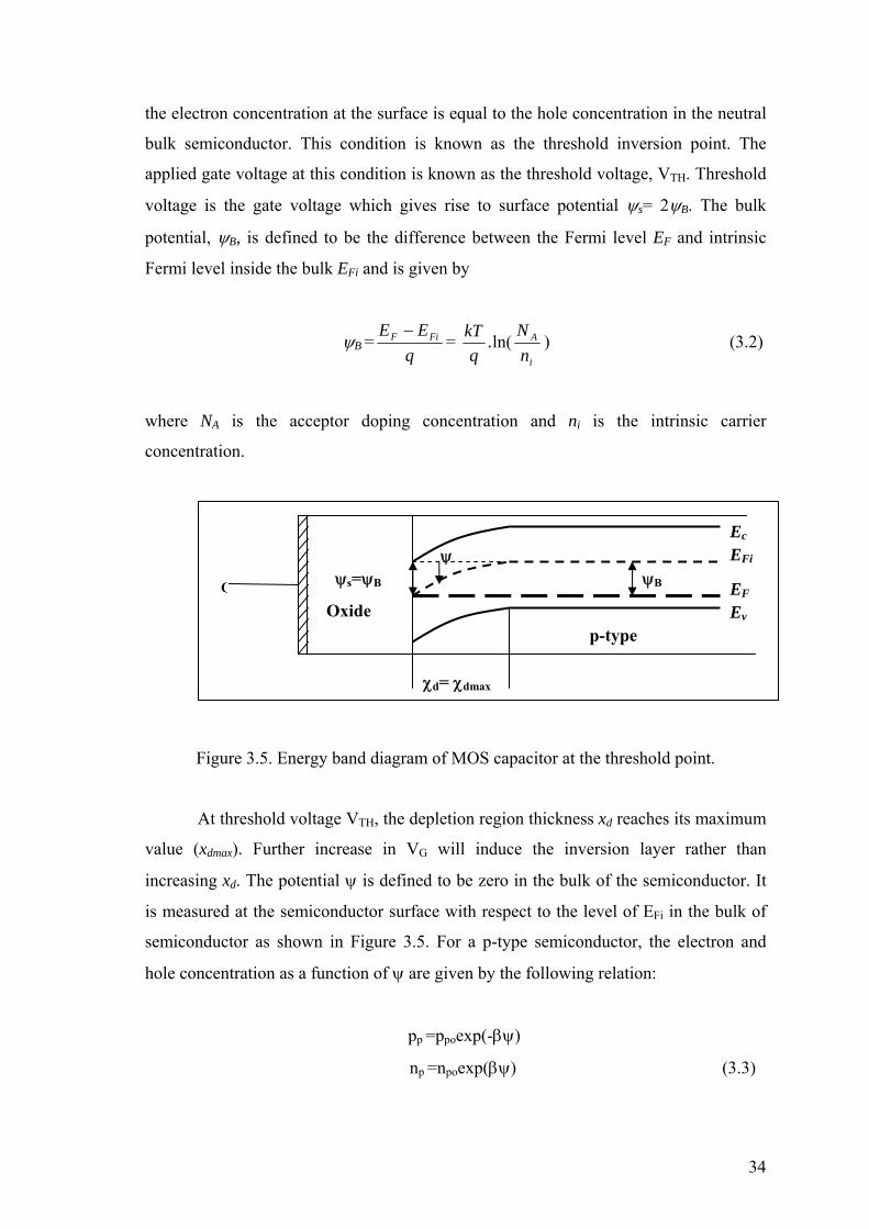
34
the electron concentration at the surface is equal to the hole concentration in the neutral
bulk semiconductor. This condition is known as the threshold inversion point. The
applied gate voltage at this condition is known as the threshold voltage, VTH. Threshold
voltage is the gate voltage which gives rise to surface potential ψs= 2ψB. The bulk
potential, ψB, is defined to be the difference between the Fermi level EF and intrinsic
Fermi level inside the bulk EFi and is given by
ψB = qEE FiF −
= q
kT .ln(i
A
nN ) (3.2)
where NA is the acceptor doping concentration and ni is the intrinsic carrier
concentration.
Figure 3.5. Energy band diagram of MOS capacitor at the threshold point.
At threshold voltage VTH, the depletion region thickness xd reaches its maximum
value (xdmax). Further increase in VG will induce the inversion layer rather than
increasing xd. The potential ψ is defined to be zero in the bulk of the semiconductor. It
is measured at the semiconductor surface with respect to the level of EFi in the bulk of
semiconductor as shown in Figure 3.5. For a p-type semiconductor, the electron and
hole concentration as a function of ψ are given by the following relation:
pp =ppoexp(-βψ)
np =npoexp(βψ) (3.3)
Ec
EFi
EF
Ev
ψ ψs=ψB
Oxide
ψB
χd= χdmax
p-type
O
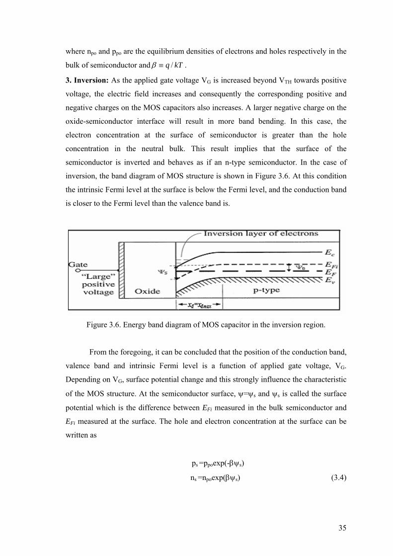
35
where npo and ppo are the equilibrium densities of electrons and holes respectively in the
bulk of semiconductor and kTq /≡β .
3. Inversion: As the applied gate voltage VG is increased beyond VTH towards positive
voltage, the electric field increases and consequently the corresponding positive and
negative charges on the MOS capacitors also increases. A larger negative charge on the
oxide-semiconductor interface will result in more band bending. In this case, the
electron concentration at the surface of semiconductor is greater than the hole
concentration in the neutral bulk. This result implies that the surface of the
semiconductor is inverted and behaves as if an n-type semiconductor. In the case of
inversion, the band diagram of MOS structure is shown in Figure 3.6. At this condition
the intrinsic Fermi level at the surface is below the Fermi level, and the conduction band
is closer to the Fermi level than the valence band is.
Figure 3.6. Energy band diagram of MOS capacitor in the inversion region.
From the foregoing, it can be concluded that the position of the conduction band,
valence band and intrinsic Fermi level is a function of applied gate voltage, VG.
Depending on VG, surface potential change and this strongly influence the characteristic
of the MOS structure. At the semiconductor surface, ψ=ψs and ψs is called the surface
potential which is the difference between EFi measured in the bulk semiconductor and
EFi measured at the surface. The hole and electron concentration at the surface can be
written as
ps =ppoexp(-βψs)
ns =npoexp(βψs) (3.4)

36
then using the value of ψs, different condition can be defined as
ψs<0 Accumulation of holes (bands bend upward)
ψs=0 Flat-band condition
ψB>ψs Depletion of holes (bands bend downward)
ψs=2ψB Midgap with ns=ps=ni (intrinsic concentration) ψs>2ψB Inversion (electron enhancement, bands bend downward further)
A great deal of information about the MOS system can be obtained from the
capacitance- voltage characteristic of the MOS capacitors and the calculation of the total
capacitance of the MOS system under different bias conditions will be explained in
detail in the following section of this chapter.
3.2 Theoretical Capacitance of Ideal MOS Structure
The analysis of small-signal capacitance of the MOS structure provides valuable
insight into the electrical behavior of the oxide-silicon interface and its technology. The
measured C-V curve can be compared with an ideal calculated C-V curve that is free of
interface states and oxide charges. The differences between these two curves can be
used to extract Dit and effective oxide charges. The calculation of the ideal C-V curve
can be found in many textbooks (Nicollian and Brews, 1982; Schroder, 1998;
Cassey,1999)
As compared with parallel plate capacitor, the static and differential
capacitances differ for MOS capacitor since the charges change nonlinearly with a small
differential change in voltage across the MOS structure. However, like the parallel plate
capacitor, the differential changes in charge density occur at the edges of the oxide. For
a MOS capacitor the differential capacitance per unit area is given as:
G
Si
dVdQ
C =' (3.5)
since the gate voltage is partially dropped across the oxide and partially across the
semiconductor, VG can be written as:

37
VG= Vox +ψs (3.6)
where Vox is the oxide voltage and ψs is the surface potential. Similarly oxide voltage
can be written as:
Vox=ox
oxSi tQε'
(3.7)
The differential capacitance per unit area from Eq. 3.6 and Eq. 3.7 now becomes
s
Siox
dif
ddQ
CC
ψ'
/1'/1
1'+
= (3.8)
Eq. 3.8 may be written as
Sioxdif CCC '
1'1
'1
+= (3.9)
where
ox
oxox
tC
ε=' and
s
SiSi d
dQC
ψ'
' ≡ (3.10)
Eq. 3.9 represents the series combination of a fixed capacitance of the oxide and
the variable capacitance of the Si which depends on the applied gate voltage through ψs
as shown in Figure 3.7.
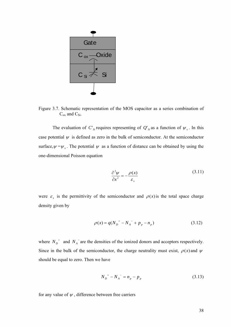
38
Figure 3.7. Schematic representation of the MOS capacitor as a series combination of Cox and CSi.
The evaluation of SiC ' requires representing of SiQ' as a function of sψ . In this
case potential ψ is defined as zero in the bulk of semiconductor. At the semiconductor
surface,ψ = sψ . The potential ψ as a function of distance can be obtained by using the
one-dimensional Poisson equation
(3.11)
were sε is the permittivity of the semiconductor and )(xρ is the total space charge
density given by
)()( ppAD npNNqx −+−= −+ρ (3.12)
where +DN and −
AN are the densities of the ionized donors and acceptors respectively.
Since in the bulk of the semiconductor, the charge neutrality must exist, )(xρ and ψ
should be equal to zero. Then we have
ppAD pnNN −=− −+ (3.13)
for any value of ψ , difference between free carriers
C ox Oxide
C Si Si
Gate
s
xx ε
ρψ )(2
2
−=∂∂

39
)exp()exp( βψβψ popopp npnp −−=− (3.14)
By replacing Eq. 3.13 and Eq. 3.14 into Eq. 3.12, the relative total space charge
density, for DA NN >> , Apo Np ≈ , thus Aino Nnn /2≅ , can be obtained as
))(()( )(2
)(2
βψβψρ eNn
eNNNn
qxA
iAA
A
i−
−−−− −+−=
the resulting Poisson equation can be obtained as
(3.15)
Integration Eq. 3.15 from the bulk toward the surface obtained as
ψε
ψψ ψβψβψ
ψ
deNn
eqNx
dx A
i
s
Ax
∫∫⎥⎥⎦
⎤
⎢⎢⎣
⎡−⎟
⎟⎠
⎞⎜⎜⎝
⎛−−⎟
⎟⎠
⎞⎜⎜⎝
⎛−=⎟
⎠⎞
⎜⎝⎛∂∂
⎟⎠⎞
⎜⎝⎛∂∂
−−
−∂∂
0
2/
0
)1()1( . (3.16)
Eq 3.16 gives the relation between the electric field SiE ( xESi ∂−∂= /ψ ) and
the surface potential sψψ = :
( )⎥⎥⎦
⎤
⎢⎢⎣
⎡−−⎟
⎟⎠
⎞⎜⎜⎝
⎛+−+⎟
⎟⎠
⎞⎜⎜⎝
⎛⎟⎟⎠
⎞⎜⎜⎝
⎛= −
−−
1)1(2222
2 βψβψε
βψβψ eNn
ekTNq
qkTE
A
i
s
ASi . (3.17)
here the following abbreviations should be introduced:
2/122
)1()1(,⎥⎥⎦
⎤
⎢⎢⎣
⎡−−⎟
⎟⎠
⎞⎜⎜⎝
⎛+−+≡⎟
⎟
⎠
⎞
⎜⎜
⎝
⎛
⎟⎟⎠
⎞⎜⎜⎝
⎛−
−− βψβψβψ βψβψ e
Nn
eNn
FA
i
A
i . (3.18)
and
2s
DA
kTLq N
ε−≡ (3.19)
)].1()1([2
2
2
−−−−=∂∂
−−− βψβψ
εψ e
Nn
eNqx A
iA
s
40
DL is called the extrinsic Debye length for holes and represent the distance over
which the free carriers reduce the potential from the fixed impurity ions. DL govern the
majority carrier deviation from the dopant concentration. Thus the electric field
becomes as
⎟⎟
⎠
⎞
⎜⎜
⎝
⎛
⎟⎟⎠
⎞⎜⎜⎝
⎛±= −
2
,2
A
i
DSi N
nF
qLkTE βψ (3.20)
For a static electric field, the space charge per unit area is related to the field through the
Gauss law by SisSi EQ ε= which gives
⎟⎟
⎠
⎞
⎜⎜
⎝
⎛
⎟⎟⎠
⎞⎜⎜⎝
⎛±= −
2
,2
A
i
D
sSi N
nF
qLkT
Q βψε
(3.21)
where a positive sign (+) is applied for the accumulation and a negative sign (-) for the
depletion. A typical variation of space charge density in the semiconductor is controlled
by F function. SiQ as a function of surface potential sψ for a p-type silicon with
NA=1.2x1015 cm-3 at room temperature is shown in Figure 3.8. For negative sψ , SiQ is
positive and corresponds to accumulation region. The dominant factor in F function is
~ )2/exp( kTIqI sψ . Flat band condition occurs at 0=sψ . For 0>> sB ψψ , SiQ is
negative and this case corresponds to depletion region and the dominant factor in F
function is ~ sψ . Inversion case occurs at Bs ψψ >> . In this condition SiQ is governed
by )2/exp( kTq sψ .

41
Figure 3.8. Variation of the space charge density SiQ' in the semiconductor as a
function of the surface potential sψ for a p-type Si with −AN =1.2x1015 cm-3
at room temperature.
The variable capacitance of silicon given in Eq. 3.10 is obtained taking
derivative of Eq. 3.21 over sψ as
( )
⎟⎟
⎠
⎞
⎜⎜
⎝
⎛
⎟⎟⎠
⎞⎜⎜⎝
⎛
⎥⎥⎦
⎤
⎢⎢⎣
⎡−⎟
⎟⎠
⎞⎜⎜⎝
⎛+−
=
−
−−
2
2
'
,
11
2
A
is
A
i
D
sSi
Nn
F
eNn
e
LC
ss
βψ
ε
βψβψ
(3.22)
At flat-band condition, where sψ =0, flat-band capacitance for silicon
substrate, 'FBC can be obtained by expanding the exponential terms into series as
fallows;

42
D
sFB L
Cε
=' . (3.23)
Then the differential capacitance of MOS system given in Eq. 3.9 can be obtained as
D
s
oxox
oxFB
LtC
εεε
+= . (3.24)
Combination of Eq. 3.6, Eq. 3.9, and Eq. 3.20 gives the complete description of
the ideal MOS structure as shown in figure 3.9. For the negative applied gate voltage
there is an accumulation of holes and the total differential capacitance is close to oxide
capacitance. As the negative gate voltage decreases a depletion region is formed. This
region is the region where the total differential capacitance decreases. The capacitance
goes through a minimum and then increases again as the inversion layer of electrons
form at the surface of the semiconductor. Finally depending on the applied frequency
two different behavior of MOS structure can be observed. At very small frequencies
between 5 to 100 Hz, the electron concentration at the surface of the surface of
semiconductor has the ability to follow the applied ac voltage and this lead to charge
exchange with the inversion layer. Thus the total differential capacitance increases and
reaches back its maximum value as seen in Figure 3.9a. However for frequency higher
than 100 Hz since the electron could not follow the signal no increase in total
differential capacitance can be observed as shown in Figure 3.9b.

43
4 2 0 2 40 .0
0 .2
0 .4
0 .6
0 .8
.0
C F B (F la t band capac itnce)
(a ) Low frequency
(b ) H igh frequency
C m in
C ox
A ccu m u latio n
D ep le tio n
In vers io n
Figure 3.9. Normalized Theoretical ideal MOS structure C-V curve for accumulation,
depletion and inversion region
3.3 Non-Ideal MOS Capacitor
In the above discussion concerning C-V characteristics we have assumed that
there is zero charge trapped in the oxide and also there is no charge trapped at the oxide-
semiconductor interface which are known as non ideal effect. In this section the non
ideal effect and its analysis will be discussed.
3.3.1 Non-Ideal Effect
In an actual MOS capacitor there are several non-ideal effects which affect the
conduction mechanism of the capacitor. These non-ideal effects are oxide charges,
interface trap charges and the work function difference between metal and
semiconductor. Figure 3.10 shows the common terminology for oxide and interface
charge. Oxide charges can be collected in three groups as fixed oxide charge ( fQ ),
oxide trapped charge ( otQ ) and mobile ionic charge ( mQ ).

44
Fixed oxide charge Q 'f , is due to structural defect in the oxide layer less than
25A o from the oxide/Si interface. This is a positive charge and its density is related to
the oxidation process.
Oxide trap charge Q 'ot , can be obtained as positive or negative due to holes or
electrons trapped in the bulk of the insulator. This trapped charge may result from
ionizing radiation or avalanche injection.
The mobile ionic charge, Q 'm , is obtained because of the ionic impurities such as
Li + , Na + , and K + .
These charges may alter the threshold voltage, silicon surface potential and
thereby change reverse leakage current and finally affects the avalanche breakdown
voltage. The sum of these oxide charges is called effective oxide charge Qeff (and its
number density Neff
) as given in Equation 3.25.
otmfeff QQQQ ++= (3.25)
Interface trapped charges itQ and more importantly interface trap charge
density, itD , plays the major role in the operation of MOS devices. These charges cause
the recombination of free carriers in the conduction and valence bands. These charges
present in the structure due to structural and oxidation-induced defects such as, metal
impurities, radiation or bond-breaking process. And they have been shown to exist
within the forbidden gap due to interruption of the periodic lattice structures of the
surface of a crystal. The interface trap charge can be obtained as positive or negative
and they are in electrical communication with the underlying Si. This charge can also be
called as surface states, fast states or interface states.

45
Figure 3.10. Schematic illustration of non-ideal effects present in Metal-Oxide-Si
system.
On the other hand, the work function differences exist due to changes in doping
concentration of p-type substrate which modifies the position of Fermi level in
semiconductor. The workfunction differences can be overcome by applying external
gate voltage which produce flat band and is represented as VoFB. And as it was
mentioned at section 3.1, flat band voltage is the work function differences of MOS
structure without oxide or interface trapped charges which is given as
)2
( BmsmmsFBo
qEV ψχ ±+−Φ=Φ−Φ=Φ= (3.26)
However, because of the doping level of the semiconductor and other non ideal
effect, here VoFB is not zero, instead it can be positive or negative number which gives
the polarity connected to the metal to obtain the flat band condition.
The non ideal effects, mentioned above changes all the characteristics of the
MOS capacitor. A great deal of information about these non-ideal effects present in
MOS capacitors can be obtained from the capacitance-voltage characteristics of MOS
device. The density of effective oxide charge is obtained from the flat band VFB voltage
shift and the density of interface trap charges is calculated from the Therman’s method
Metal
Insulator
SiInterface trap Charge, Qit
Oxide trap. Charge, Qot
Mobile ionic Charge, Qm
Fixed oxide Charge, Qf
+ + + +
+ + +- - -
Na+
K+

46
“(Nicollian and Brews, 1982)”. In order to determine the quality of the gate oxide, these
curves with Therman’s method are used extensively as a diagnostic tool.
3.3.2 Calculation of Flat Band Voltage, Doping concentration and the
Effective Oxide Charge
In the previous section, effective oxide charges were described in detail. These
charges affect the experimental C-V curve of MOS capacitor. They cause a shift of the
ideal MOS curve along the voltage axis. Consequently a larger voltage is required to set
up the surface potential ψs on semiconductor surface. The new flat band voltage with
these oxide charges can be obtained as
ox
effoFB
ox
effmsFB C
QV
CQ
V '' +=+Φ= (3.27)
where Φms is work function differences as defined in Eq. 3.26. Qeff is effective oxide
charge as defined in Eq. 3.25and Cox is the oxide capacitance.
One of the methods to obtain flat band voltage is to plot experimentally obtained
(1/C2) versus VG curve. This curve provides with flat band voltage and doping
concentration NA of p-type substrate. An example of (1/C2) versus VG is shown in
Figure 3.11. The intercept point in the voltage axis is the flat band voltage VFB, and the
slope of the curve gives the doping concentration.

47
Figure 3.11. 1/C2 versus VG curve of a MOS capacitor
In accumulation and inversion, free carrier charge density is only weakly
dependent on doping concentration. Therefore doping concentration cannot be obtained
accurately in either accumulation or inversion. Therefore it can be obtained accurately
in depletion, where free carrier concentration strongly depends on doping concentration.
The slope in Figure 3.11 is taken for depletion region. Doping concentration is
calculated using the following equation
1
2
12−
−⎥⎦
⎤⎢⎣
⎡⎟⎠⎞
⎜⎝⎛−=
CdVdqN
GsA ε (3.28)
Eq. 3.28 shows that −AN is related reciprocally to the slope of a (1/C2) versus
VG curve. A positive slope will give a negative −AN from Eq. 3.28 for acceptors
whereas a negative slope gives a positive −AN for donors.
Another common method of measuring the flat band voltage VFB is comparing
experimental and theoretical (ideal) C-V curves. The theoretical C-V curve is
calculated for a device without work function difference or oxide charges together with
N -A ~ r e c ip r o c a l o f t h e s lo p e

48
the oxide thickness, dielectric constant and doping concentration NA obtained from the
experimental C-V curve of the same MOS device. Then both C-V curves are plotted
together on the same figure. The shift of experimental capacitance from that at VG=0
Volt is indicated as the flat band voltage shift VFB as shown in Figure 3.12. For each
MOS device, the VFB values are obtained by using the 1/C2 vs VG curve and from the
comparison of both ideal and experimental C-V curves. Consistent values of VFB are
obtained from both method within the experimental and human error.
Figure 3.12. Theoretical and experimental high Frequency C-V curves of a MOS capacitor with p-type silicon substrate.
Once the flat band voltage is obtained from the shift of theoretical and
experimental C-V curves, effective oxide charge Qeff and its number density Neff are
calculated using the equation given below:
qVVC
N FBFBo
oxeffeff
)(' −== (3.29)
In addition, some of the charges presented in the oxide are mobile trap charges
and follows the sign of applied gate voltage. They move toward metal gate or to
VG(Volt)-5 -4 -3 -2 -1 0 1 2
C/C
ox
0
1
VFB
ΨS=0
VG=0
Φms=0ExperimentalTheoretical
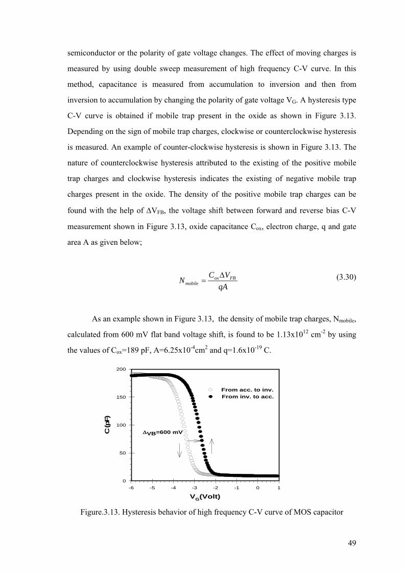
49
semiconductor or the polarity of gate voltage changes. The effect of moving charges is
measured by using double sweep measurement of high frequency C-V curve. In this
method, capacitance is measured from accumulation to inversion and then from
inversion to accumulation by changing the polarity of gate voltage VG. A hysteresis type
C-V curve is obtained if mobile trap present in the oxide as shown in Figure 3.13.
Depending on the sign of mobile trap charges, clockwise or counterclockwise hysteresis
is measured. An example of counter-clockwise hysteresis is shown in Figure 3.13. The
nature of counterclockwise hysteresis attributed to the existing of the positive mobile
trap charges and clockwise hysteresis indicates the existing of negative mobile trap
charges present in the oxide. The density of the positive mobile trap charges can be
found with the help of ΔVFB, the voltage shift between forward and reverse bias C-V
measurement shown in Figure 3.13, oxide capacitance Cox, electron charge, q and gate
area A as given below;
qA
VCN FBox
mobileΔ
= (3.30)
As an example shown in Figure 3.13, the density of mobile trap charges, Nmobile,
calculated from 600 mV flat band voltage shift, is found to be 1.13x1012 cm-2 by using
the values of Cox=189 pF, A=6.25x10⁻⁴cm2 and q=1.6x10⁻¹⁹ C.
Figure.3.13. Hysteresis behavior of high frequency C-V curve of MOS capacitor
VG(Volt)-6 -5 -4 -3 -2 -1 0 1
C (p
F)
0
50
100
150
200
From acc. to inv.From inv. to acc.
ΔVB=600 mV

50
3.3.3 Extraction of Density of Interface Trap States (Dit)
Interface defect states, or interface traps, are the defects located at the interface
between the Si substrate and the gate dielectric layer. Interface trap density, Dit, depends
on the gate dielectric material as well as the fabrication technique. Dit is a crucial
parameter for the effectiveness of the fabrication process as well as the device
performance. In this section methods used to derive the Dit levels of MOS capacitor are
explained in detail. These are high frequency C-V method known as Terman’s method
and simultaneous C-V method.
3.3.3.1 High Frequency Capacitance-Voltage Method (Terman’s
Method)
High frequency C-V method was first used by Terman to calculate Dit levels. In
this method, both high frequency experimental and theoretical (ideal) capacitance-
voltage curves are used to calculate Dit levels. Here both experimental and theoretical
C-V curves are normalized to the oxide capacitance Cox to compare the effects of
interface trap states. In Figure 3.14 an example of both experimental C/Cox versus VG
and theoretical C/Cox versus surface potential ψs are shown together. In ideal C/Cox
curve, there is no effect due to interface traps charges, however, experimental C/Cox
curve shifts along voltage axis due to interface trap present in actual MOS devices. By
comparing these curves, the effect of interface traps on C-V curve is obtained by
obtaining the functional dependence of surface potential ψs on gate voltage VG for every
C/Cox normalized capacitance values shown in Figure 3.14. Theoretical C versus ψs
values are calculated by using the Eq. 3.13 through 3.22 given in this chapter.
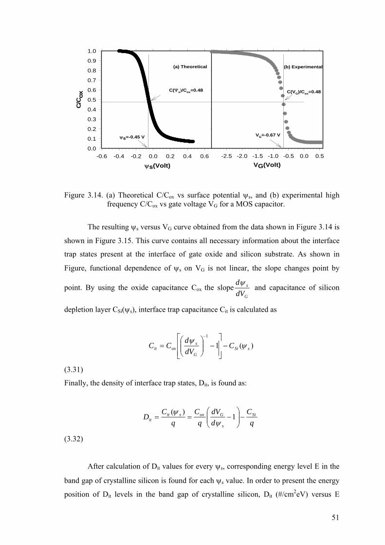
51
Figure 3.14. (a) Theoretical C/Cox vs surface potential ψs, and (b) experimental high frequency C/Cox vs gate voltage VG for a MOS capacitor.
The resulting ψs versus VG curve obtained from the data shown in Figure 3.14 is
shown in Figure 3.15. This curve contains all necessary information about the interface
trap states present at the interface of gate oxide and silicon substrate. As shown in
Figure, functional dependence of ψs on VG is not linear, the slope changes point by
point. By using the oxide capacitance Cox the slopeG
s
dVdψ
and capacitance of silicon
depletion layer CSi(ψs), interface trap capacitance Cit is calculated as
)(11
sSiG
soxit C
dVd
CC ψψ
−⎥⎥⎦
⎤
⎢⎢⎣
⎡−⎟⎟
⎠
⎞⎜⎜⎝
⎛=
−
(3.31)
Finally, the density of interface trap states, Dit, is found as:
q
CddV
qC
qC
D Si
s
Goxsitit −⎟⎟
⎠
⎞⎜⎜⎝
⎛−== 1
)(ψ
ψ
(3.32)
After calculation of Dit values for every ψs, corresponding energy level E in the
band gap of crystalline silicon is found for each ψs value. In order to present the energy
position of Dit levels in the band gap of crystalline silicon, Dit (#/cm2eV) versus E
ψs(Volt)-0.6 -0.4 -0.2 0.0 0.2 0.4 0.6
C/C
ox
0.0
0.1
0.2
0.3
0.4
0.5
0.6
0.7
0.8
0.9
1.0
VG(Volt)-2.5 -2.0 -1.5 -1.0 -0.5 0.0 0.5
(a) Theoretical (b) Experimental
C(Ψs)/Cox=0.48
ψs=-0.45 V VG=-0.67 V
C(VG)/Cox=0.48
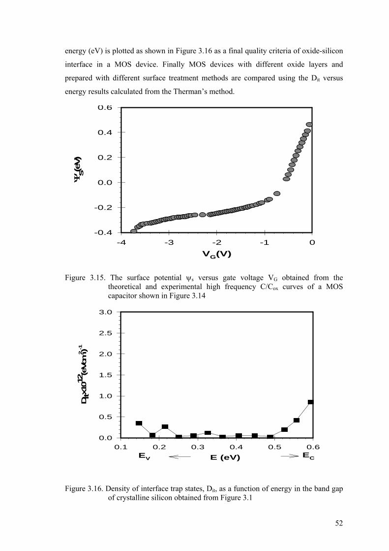
52
energy (eV) is plotted as shown in Figure 3.16 as a final quality criteria of oxide-silicon
interface in a MOS device. Finally MOS devices with different oxide layers and
prepared with different surface treatment methods are compared using the Dit versus
energy results calculated from the Therman’s method.
Figure 3.15. The surface potential ψs versus gate voltage VG obtained from the
theoretical and experimental high frequency C/Cox curves of a MOS capacitor shown in Figure 3.14
Figure 3.16. Density of interface trap states, Dit, as a function of energy in the band gap
of crystalline silicon obtained from Figure 3.1
VG(V)-4 -3 -2 -1 0
Ψs(
eV)
-0.4
-0.2
0.0
0.2
0.4
0.6
E (eV)0.1 0.2 0.3 0.4 0.5 0.6
Ditx
1012
(eVc
m2 )-1
0.0
0.5
1.0
1.5
2.0
2.5
3.0
EV EC
53
3.3.3.2 Combined High-Low Frequency Capacitance Method-
Simultaneous Capacitance –Voltage Spectroscopy
The calculation of the ideal C-V curve is not only time consuming, but also
introduces uncertainty for very thin gate dielectrics. Combination of a high frequency
C-V curve with a low frequency C-V curve which avoids the ideal C-V calculation was
first achieved by Costagne and Vapile (Nicollian and Brews, 1982). Theoretical
computation of CSi and measurement of doping profile is eliminated in this method.
From high frequency C-V, high frequency capacitance CHF is obtained as;
Siox
SioxHF CC
CCC
+= (3.33)
Then, CSi is derived as;
HFox
HFoxSi CC
CCC
−= (3.34)
At low frequencies, interface trap capacitance Cit can be extracted from the measured
low frequency capacitance if CSi and Cox are known. The relation between these
capacitances can be written as
itSioxLF CCCC +
+=111 (3.35)
where CLF is the low frequency capacitance measured at gate bias VG. Solving Eq. 3.34
for Cit yields
Sioxlf
it CCC
C −⎥⎥⎦
⎤
⎢⎢⎣
⎡−=
−111 (3.36)
where Cox can be measured in strong accumulation. Combining Eq. 3.34 and Eq 3.36
yields

54
HFox
HFox
oxlfit CC
CCCC
C−
−⎥⎥⎦
⎤
⎢⎢⎣
⎡−=
−111 (3.37)
In this way Cit is obtained directly from the measured C-V curves, without the
uncertainty introduced by a theoretical CSi and without uncertainty as to whether CSi has
been calculated for the correct band bending. The density of interface states, Dit, is
calculated with the help of Eq. 3.32 where Dit= Cit/q together with Eq.3.37.Examples of
CHF and CLF versus VG and Dit versus E obtained from both Terman’s method and
simultaneous C-V method are shown in Figure 3.17 and Figure3.18, respectively.
For samples with SiO2, the density of interface trap states obtained from both
Terman’s method and Simultaneous C-V method are agree very well as shown in Figure
3.18 and the experimental error is within the limit of %10. However, as discussed
before, a low frequency C-V curve is not always available for an ultra thin high k gate
dielectric layer with a large leakage current. In addition, the leakage current, which
either adds to or subtracts from the displacement current, usually distorts the resulting
C-V curve. Therefore accumulation capacitance is not exactly the same as the inversion
capacitance (Schroder, 1998). Due to these reasons, Simultaneous C-V method could
not be carried out for high-k gate oxide.
In this thesis, the density of interface trap states of Al-SiO2-Si MOS capacitors
are evaluated by using both Terman’s method and combined high and low frequency
method. However, for the determination of interface trap states of Metal-Ta2O5-Si MOS
capacitors only Terman’s method is used. The details about the results will be given in
the next chapter.
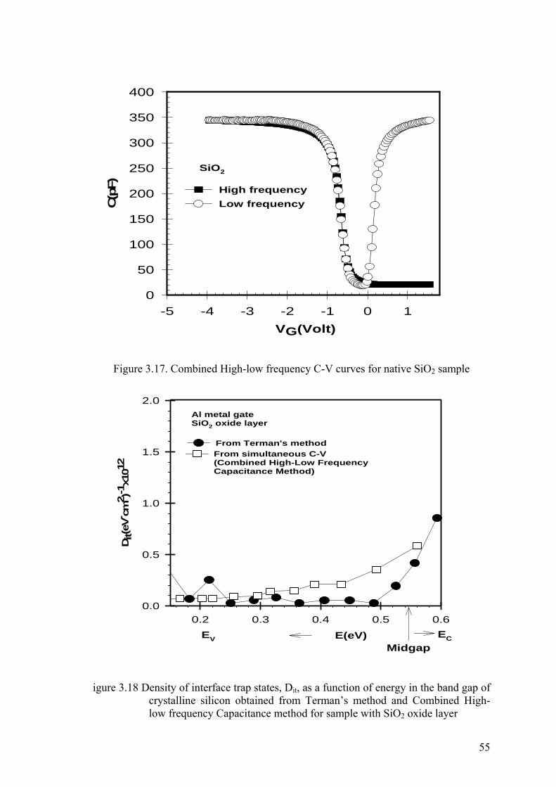
55
Figure 3.17. Combined High-low frequency C-V curves for native SiO2 sample
igure 3.18 Density of interface trap states, Dit, as a function of energy in the band gap of
crystalline silicon obtained from Terman’s method and Combined High-low frequency Capacitance method for sample with SiO2 oxide layer
E(eV)0.2 0.3 0.4 0.5 0.6
Dit(
eV- c
m2 )
-1x1
012
0.0
0.5
1.0
1.5
2.0Al metal gateSiO2 oxide layer
From simultaneous C-V(Combined High-Low FrequencyCapacitance Method)
From Terman's method
EV ECMidgap
VG(Volt)-5 -4 -3 -2 -1 0 1
C(p
F)
0
50
100
150
200
250
300
350
400
High frequencyLow frequency
SiO2
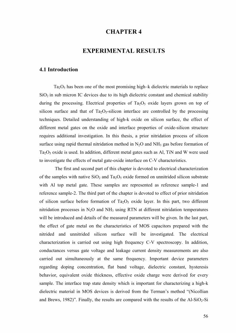
56
CHAPTER 4
EXPERIMENTAL RESULTS
4.1 Introduction
Ta2O5 has been one of the most promising high–k dielectric materials to replace
SiO2 in sub micron IC devices due to its high dielectric constant and chemical stability
during the processing. Electrical properties of Ta2O5 oxide layers grown on top of
silicon surface and that of Ta2O5-silicon interface are controlled by the processing
techniques. Detailed understanding of high-k oxide on silicon surface, the effect of
different metal gates on the oxide and interface properties of oxide-silicon structure
requires additional investigation. In this thesis, a prior nitridation process of silicon
surface using rapid thermal nitridation method in N2O and NH3 gas before formation of
Ta2O5 oxide is used. In addition, different metal gates such as Al, TiN and W were used
to investigate the effects of metal gate-oxide interface on C-V characteristics.
The first and second part of this chapter is devoted to electrical characterization
of the samples with native SiO2 and Ta2O5 oxide formed on unnitrided silicon substrate
with Al top metal gate. These samples are represented as reference sample-1 and
reference sample-2. The third part of the chapter is devoted to effect of prior nitridation
of silicon surface before formation of Ta2O5 oxide layer. In this part, two different
nitridation processes in N2O and NH3 using RTN at different nitridation temperatures
will be introduced and details of the measured parameters will be given. In the last part,
the effect of gate metal on the characteristics of MOS capacitors prepared with the
nitrided and unnitrided silicon surface will be investigated. The electrical
characterization is carried out using high frequency C-V spectroscopy. In addition,
conductances versus gate voltage and leakage current density measurements are also
carried out simultaneously at the same frequency. Important device parameters
regarding doping concentration, flat band voltage, dielectric constant, hysteresis
behavior, equivalent oxide thickness, effective oxide charge were derived for every
sample. The interface trap state density which is important for characterizing a high-k
dielectric material in MOS devices is derived from the Terman’s method “(Nicollian
and Brews, 1982)”. Finally, the results are compared with the results of the Al-SiO2-Si

57
and Al-Ta2O5-Si MOS capacitors as reference sample-1 and reference sample-2,
respectively.
4.2 Results of Al-SiO2-Si MOS capacitor; Reference Sample-1
The experimental high frequency and low frequency C-V measurement of four
different dots of Al-SiO2-Si MOS capacitor for the same substrate are shown in Figure
4.1. In the accumulation, both low and high frequency C-V curves overlap, giving the
value of oxide capacitance until depletion region. Both curves overlap at negative
voltages but they show expected deviation in inversion region, where high frequency C-
V curve shows saturation at minimum capacitance value. However, low frequency C-V
curve increases until it reaches to accumulation capacitance value. The oxide
capacitance, Cox, was obtained around 350 pF. The relative dielectric constant was
calculated from the Cox and measured thickness and capacitor area. It is found to be 3.95
as expected for the native oxide SiO2.
Experimental high frequency C-V curve contains both ideal and non-ideal
effects. One of these non-ideal effects in MOS capacitors is the mobile trapped charges.
The effect of mobile trapped charges is seen in the hysteresis effect on C-V curve. For
this reason, high frequency C-V curve is measured from accumulation to inversion and
reversed back to accumulation. After this measurement cycle, depending on the nature
of mobile trapped charges present in the oxide, C-V curve shows a shift along clockwise
or counterclockwise. The hysteresis effect of dot-2 of Al-SiO2-Si capacitors is shown in
Figure 4.2. It is seen that C-V curves for both measurement cycles overlap quite well,
giving ΔVFB shift less than 30 mV. This indicates that native oxide SiO2 is close to
electronic quality, for which ΔVFB is around 20 mV as reported in literature (T. P. Ma,
1997).
Other non ideal effects contributing to high frequency C-V curve of MOS
capacitors are work function differences, effective oxide charges and interface trap
states. In order to determine the oxide and oxide-silicon interface quality, theoretical
(ideal) capacitance-voltage curve of the MOS capacitor is calculated using the

58
Figure 4.1. Experimental High-Low frequency capacitance versus gate voltage curves of Al- SiO2-Si MOS capacitors; reference sample
Figure 4.2. Forward and reverse C-V curve of Al- SiO2-Si MOS capacitor with unnitrided Si surface
VG(Volt)
-4 -3 -2 -1 0 1 2
C(p
F)
0
50
100
150
200
250
300
350
Experimentalhigh frequency
Dot-1
Dot-3
Dot-2
Dot-4
Reference Sample-1
low frequency
Dot-1
Dot-3
Dot-2
V G ( V o l t )- 5 - 4 - 3 - 2 - 1 0 1 2
C (p
F)
0
5 0
1 0 0
1 5 0
2 0 0
2 5 0
3 0 0
3 5 0
F r o m a c c . t o in v .
F r o m in v . t o a c c .
h ig h f r e q u e n c y
lo w f r e q u e n c y
f r o m a c c . t o in v .
F r o m in v . t o a c c .

59
experimental value of doping concentration NA of silicon substrate, oxide thickness and
metal gate area. Doping concentration is obtained from the slope of 1/C2 versus gate
voltage as presented in Figure 4.3. For four different dots, according to equation 3.28,
given in Chapter 3, the slope of curves gives the value of NA to be 9x1014 cm-3. The
intercept of the slope on the VG axis indicates the shift of flat band voltage VFB due to
non-ideal effects.
Ideal and experimental high frequency C-V curves (normalized to oxide capacitance
Cox) of one of the MOS capacitor are presented in Figure 4.4. It is seen that
experimental C-V curve (symbols) shift to negative voltages due to effective oxide
charges present in the oxide layer. The amount of shift, VFB, is measured from VG=0
volt at ideal curve to experimental C-V curve. The VFB value obtained from Figure 4.4
is around 0.6 volt, which is almost identical to that found from the intercept of slope
1/C2 vs VG shown in Figure 4.3. In addition, further confirmation of VFB voltage is
found from the Conductance versus VG curve simultaneously measured at 1 MHz
frequency. In Figure 4.4, conductance G versus gate voltage VG of the sample is
presented on the same figure that it shows a maximum value around the flat band
voltage, VFB, as expected for the MOS capacitor. As seen from the figure, capacitance
varies from an upper to lower value over the illustrated bias range, whereas equivalent
conductance goes through a peak and approach zero on other side. Similar results were
also obtained for other dots measured from the same substrate. It can be concluded that
experimental C-V and G-V measurements are consistent for a good quality MOS
capacitor. On the other hand, from the figure it can be seen that the conductivity of the
SiO2 insulating layer is around 20 μS which is sufficiently low for a good insulating
properties. Flat band voltage shift VFB obtained from the shift of experimental curve are
used to calculate the effective oxide charge and its number density Neff, present in the
native oxide SiO2 for all the samples using equation 3.29. Calculated Neff values are
2.9x1011 cm-2 for all the samples. These values indicate that SiO2 has lower effective
oxide charge closer to the electronic grade SiO2 levels reported in literature (Manchanda
et all, 1998).
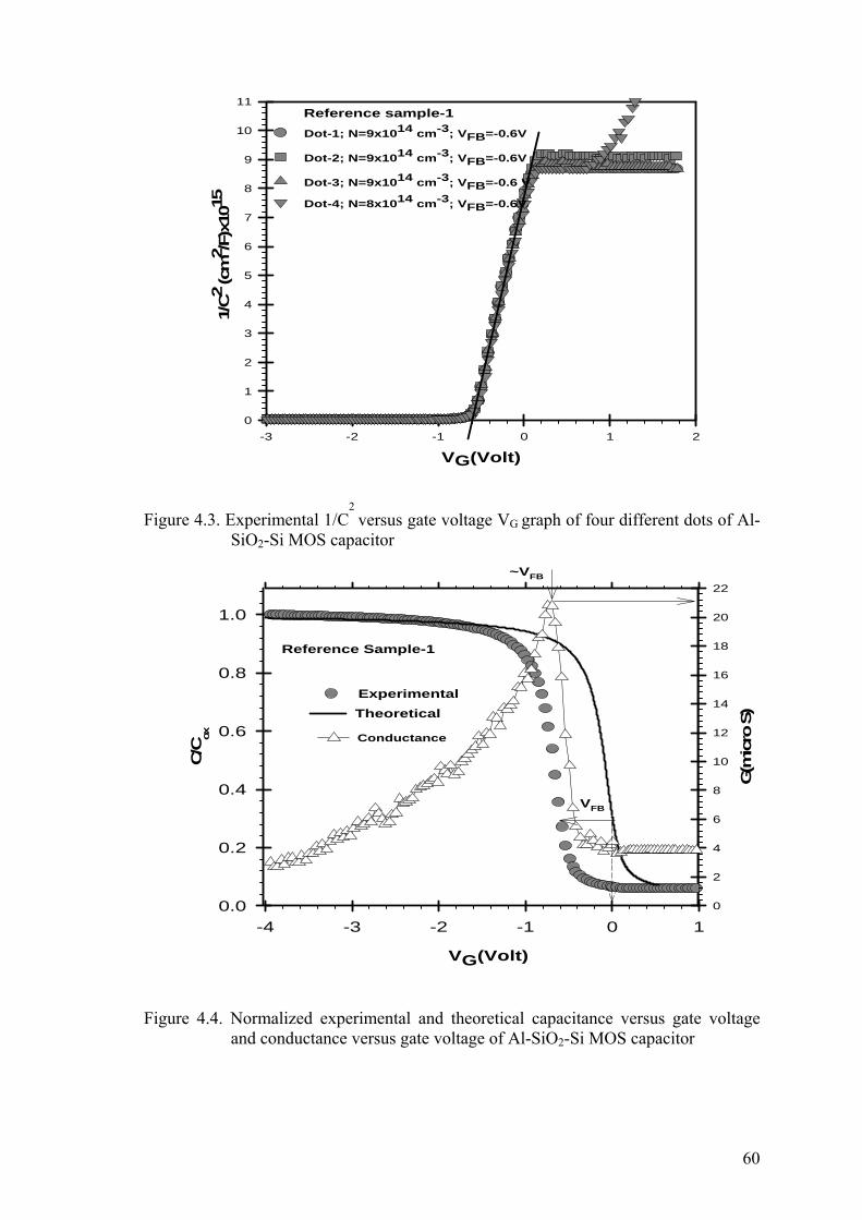
60
Figure 4.3. Experimental 1/C
2 versus gate voltage VG
graph of four different dots of Al-SiO2-Si MOS capacitor
Figure 4.4. Normalized experimental and theoretical capacitance versus gate voltage
and conductance versus gate voltage of Al-SiO2-Si MOS capacitor
VG(Volt)
-4 -3 -2 -1 0 1
C/C
ox
0.0
0.2
0.4
0.6
0.8
1.0
G(m
icro
S)
0
2
4
6
8
10
12
14
16
18
20
22
Reference Sample-1
ExperimentalTheoretical
VFB
Conductance
~VFB
VG(Volt)-3 -2 -1 0 1 2
1/C2
(cm
2 /F)
x101
5
0
1
2
3
4
5
6
7
8
9
10
11
Dot-3; N=9x1014 cm-3; VFB=-0.6 V
Dot-4; N=8x1014 cm-3; VFB=-0.6V
Dot-1; N=9x1014 cm-3; VFB=-0.6V
Dot-2; N=9x1014 cm-3; VFB=-0.6V
Reference sample-1

61
Furthermore, the most important non-ideal effect seen in MOS capacitors is the
density of interface trap states, Dit. The levels of Dit in different dots are calculated
using both Terman’s method (L. M. Terman, 1962) and simultaneous C-V method. In
Therman’s method, ideal C/Cox versus surface potential ψs and experimental C/Cox
versus gate voltage VG curves are plotted together. From these curves surface potential
ψs versus gate voltage VG curve is generated for each sample as shown in Figure 4.5. Dit
levels of the samples are then calculated using the data in Figure 4.5 and procedure
given in Chapter 3. Calculated levels of Dit for four different dots and one calculated
from simultaneous C-V method are presented in Figure 4.6 as a function of energy in
the band gap of silicon. Dit levels obtained from both method agree very well and vary
around 2±1x10¹¹ (eVcm2)-1 for all the samples. These values are presented in Table 4.1.
These values are low and closer to the value reported for electronic grade of SiO2-Si
interface (P. K. Roy and I. C. Kizilyali, 1998).
Finally, the main characteristics of a MOS capacitors used in IC technology is
the leakage current levels measurement through the oxide. Current density J versus gate
voltage curve derived from the conductance versus gate voltage curve of the same
sample is presented in Figure 4.7. The current density at VG=0 volt reaches to 60 μAcm-
2 for sample Dot-1. Other samples also show similar leakage current levels.
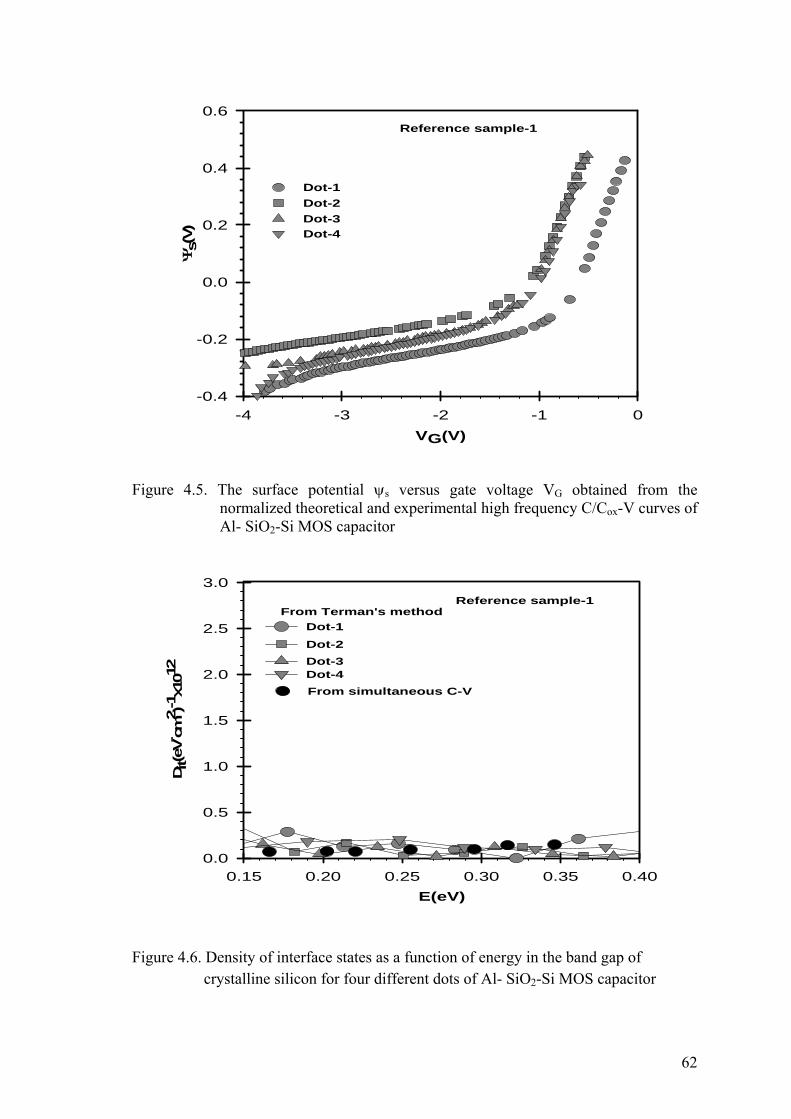
62
Figure 4.5. The surface potential ψs versus gate voltage VG obtained from the
normalized theoretical and experimental high frequency C/Cox-V curves of Al- SiO2-Si MOS capacitor
Figure 4.6. Density of interface states as a function of energy in the band gap of
crystalline silicon for four different dots of Al- SiO2-Si MOS capacitor
E(eV)0.15 0.20 0.25 0.30 0.35 0.40
Dit(
eV- c
m2 )
-1x1
012
0.0
0.5
1.0
1.5
2.0
2.5
3.0
Dot-3Dot-4
Dot-1Dot-2
Reference sample-1
From simultaneous C-V
From Terman's method
VG(V)-4 -3 -2 -1 0
-0.4
-0.2
0.0
0.2
0.4
0.6
Dot-1
Dot-3
Ψs(
V) Dot-4
Dot-2
Reference sample-1
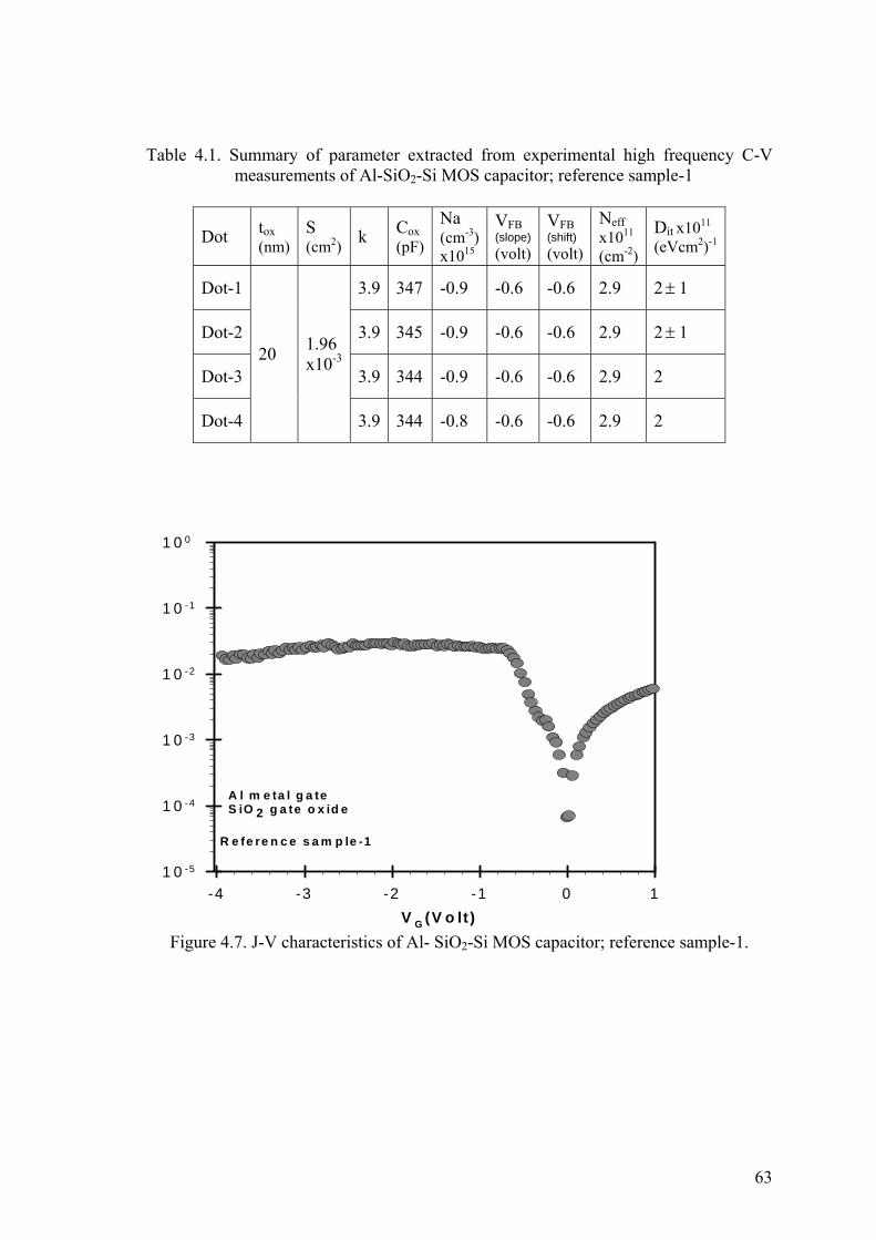
63
Table 4.1. Summary of parameter extracted from experimental high frequency C-V
measurements of Al-SiO2-Si MOS capacitor; reference sample-1
Figure 4.7. J-V characteristics of Al- SiO2-Si MOS capacitor; reference sample-1.
Dot tox (nm)
S (cm2) k Cox
(pF)
Na (cm-3) x1015
VFB (slope) (volt)
VFB (shift) (volt)
Neff x1011 (cm-2)
Dit x1011
(eVcm2)-1
Dot-1 3.9 347 -0.9 -0.6 -0.6 2.9 2± 1
Dot-2 3.9 345 -0.9 -0.6 -0.6 2.9 2± 1
Dot-3 3.9 344 -0.9 -0.6 -0.6 2.9 2
Dot-4
20 1.96 x10⁻³
3.9 344 -0.8 -0.6 -0.6 2.9 2
V G (V o lt )-4 -3 -2 -1 0 1
1 0 -5
1 0 -4
1 0 -3
1 0 -2
1 0 -1
1 0 0
A l m e ta l g a teS iO 2 g a te o x id e
R e fe re n c e s a m p le -1
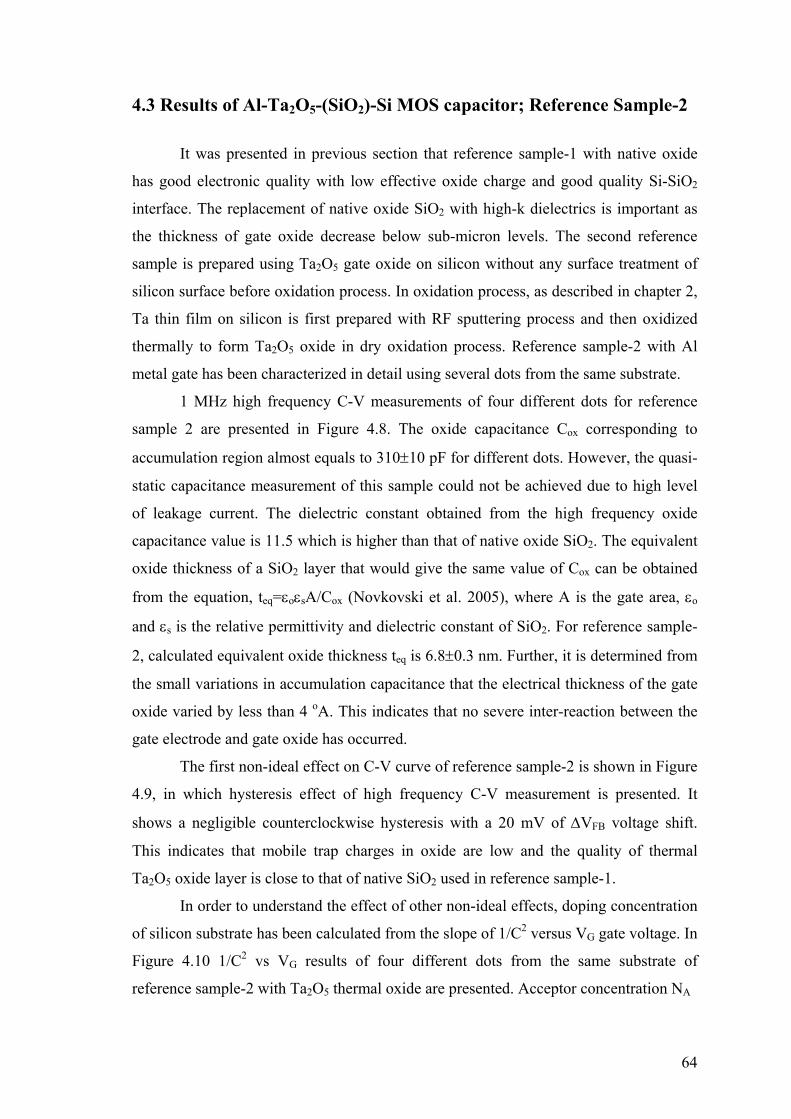
64
4.3 Results of Al-Ta2O5-(SiO2)-Si MOS capacitor; Reference Sample-2
It was presented in previous section that reference sample-1 with native oxide
has good electronic quality with low effective oxide charge and good quality Si-SiO2
interface. The replacement of native oxide SiO2 with high-k dielectrics is important as
the thickness of gate oxide decrease below sub-micron levels. The second reference
sample is prepared using Ta2O5 gate oxide on silicon without any surface treatment of
silicon surface before oxidation process. In oxidation process, as described in chapter 2,
Ta thin film on silicon is first prepared with RF sputtering process and then oxidized
thermally to form Ta2O5 oxide in dry oxidation process. Reference sample-2 with Al
metal gate has been characterized in detail using several dots from the same substrate.
1 MHz high frequency C-V measurements of four different dots for reference
sample 2 are presented in Figure 4.8. The oxide capacitance Cox corresponding to
accumulation region almost equals to 310±10 pF for different dots. However, the quasi-
static capacitance measurement of this sample could not be achieved due to high level
of leakage current. The dielectric constant obtained from the high frequency oxide
capacitance value is 11.5 which is higher than that of native oxide SiO2. The equivalent
oxide thickness of a SiO2 layer that would give the same value of Cox can be obtained
from the equation, teq=εoεsA/Cox (Novkovski et al. 2005), where A is the gate area, εo
and εs is the relative permittivity and dielectric constant of SiO2. For reference sample-
2, calculated equivalent oxide thickness teq is 6.8±0.3 nm. Further, it is determined from
the small variations in accumulation capacitance that the electrical thickness of the gate
oxide varied by less than 4 oA. This indicates that no severe inter-reaction between the
gate electrode and gate oxide has occurred.
The first non-ideal effect on C-V curve of reference sample-2 is shown in Figure
4.9, in which hysteresis effect of high frequency C-V measurement is presented. It
shows a negligible counterclockwise hysteresis with a 20 mV of ΔVFB voltage shift.
This indicates that mobile trap charges in oxide are low and the quality of thermal
Ta2O5 oxide layer is close to that of native SiO2 used in reference sample-1.
In order to understand the effect of other non-ideal effects, doping concentration
of silicon substrate has been calculated from the slope of 1/C2 versus VG gate voltage. In
Figure 4.10 1/C2 vs VG results of four different dots from the same substrate of
reference sample-2 with Ta2O5 thermal oxide are presented. Acceptor concentration NA
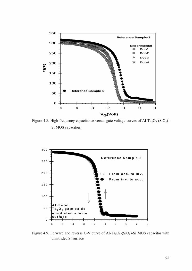
65
Figure 4.8. High frequency capacitance versus gate voltage curves of Al-Ta2O5-(SiO2)-
Si MOS capacitors
Figure 4.9. Forward and reverse C-V curve of Al-Ta2O5-(SiO2)-Si MOS capacitor with
unnitrided Si surface
-6 -5 -4 -3 -2 -1 0 1 2 30
5 0
1 0 0
1 5 0
2 0 0
2 5 0
3 0 0
F r o m a c c . to in v .
F r o m in v . to a c c .
A l m e ta lT a 2 O 5 g a te o x id eu n n it r id e d s i l ic o ns u r fa c e
R e fe r e n c e S a m p le -2
VG(Volt)
-5 -4 -3 -2 -1 0 1
C(p
F)
0
50
100
150
200
250
300
350Reference Sample-2
ExperimentalDot-1
Dot-3Dot-2
Dot-4
Reference Sample-1
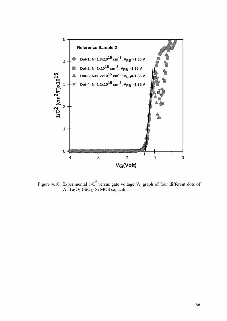
66
Figure 4.10. Experimental 1/C
2 versus gate voltage VG
graph of four different dots of Al-Ta2O5-(SiO2)-Si MOS capacitor
VG(Volt)-4 -3 -2 -1 0
1/C
2 (c
m2 /
F)x1
015
0
1
2
3
4
5
Reference Sample-2
Dot-3; N=1.2x1015 cm-3; VFB=-1.35 V
Dot-4; N=1.2x1015 cm-3; VFB=-1.35 V
Dot-1; N=1.3x1015 cm-3; VFB=-1.35 V
Dot-2; N=1x1015 cm-3; VFB=-1.35 V
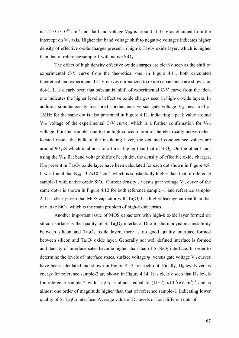
67
is 1.2±0.1x1015 cm-3 and flat band voltage VFB is around -1.35 V as obtained from the
intercept on VG axis. Higher flat band voltage shift to negative voltages indicates higher
density of effective oxide charges present in high-k Ta2O5 oxide layer, which is higher
than that of reference sample-1 with native SiO2.
The effect of high density effective oxide charges are clearly seen as the shift of
experimental C-V curve from the theoretical one. In Figure 4.11, both calculated
theoretical and experimental C-V curves normalized to oxide capacitance are shown for
dot-1. It is clearly seen that substantial shift of experimental C-V curve from the ideal
one indicates the higher level of effective oxide charges seen in high-k oxide layers. In
addition simultaneously measured conductance versus gate voltage VG measured at
1MHz for the same dot is also presented in Figure 4.11, indicating a peak value around
VFB voltage of the experimental C-V curve, which is a further confirmation for VFB
voltage. For this sample, due to the high concentration of the electrically active defect
located inside the bulk of the insulating layer, the obtained conductance values are
around 90 μS which is almost four times higher than that of SiO2. On the other hand,
using the VFB flat band voltage shifts of each dot, the density of effective oxide charges,
Neff present in Ta2O5 oxide layer have been calculated for each dot shown in Figure 4.8.
It was found that Neff =3.2x1012 cm2, which is substantially higher than that of reference
sample-1 with native oxide SiO2. Current density J versus gate voltage VG curve of the
same dot-1 is shown in Figure 4.12 for both reference sample -1 and reference sample-
2. It is clearly seen that MOS capacitor with Ta2O5 has higher leakage current than that
of native SiO2, which is the main problem of high-k dielectrics.
Another important issue of MOS capacitors with high-k oxide layer formed on
silicon surface is the quality of Si-Ta2O5 interface. Due to thermodynamic instability
between silicon and Ta2O5 oxide layer, there is no good quality interface formed
between silicon and Ta2O5 oxide layer. Generally not well defined interface is formed
and density of ınterface sates become higher than that of Si-SiO2 interface. In order to
determine the levels of interface states, surface voltage ψs versus gate voltage VG curves
have been calculated and shown in Figure 4.13 for each dot. Finally, Dit levels versus
energy for reference sample-2 are shown in Figure 4.14. It is clearly seen that Dit levels
for reference sample-2 with Ta2O5 is almost equal to (11±2) x1011(eVcm2)-1 and is
almost one order of magnitude higher than that of reference sample-1, indicating lower
quality of Si-Ta2O5 interface. Average value of Dit levels of four different dots of
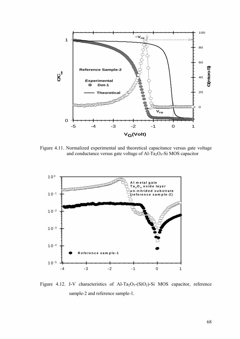
68
Figure 4.11. Normalized experimental and theoretical capacitance versus gate voltage
and conductance versus gate voltage of Al-Ta2O5-Si MOS capacitor
Figure 4.12. J-V characteristics of Al-Ta2O5-(SiO2)-Si MOS capacitor, reference
sample-2 and reference sample-1.
VG(Volt)
-5 -4 -3 -2 -1 0 1
C/C
ox
0
1
G(m
icro
S)
0
20
40
60
80
100
Reference Sample-2
ExperimentalDot-1
Theoretical
VFB
~VFB
-4 -3 -2 -1 0 11 0 -5
1 0 -4
1 0 -3
1 0 -2
1 0 -1
1 0 0
A l m e ta l g a te T a 2 O 5 o x id e la y e ru n -n it r id e d s u b s tr a te( r e fe r e n c e s a m p le -2 )
R e fe r e n c e s a m p le -1

69
Figure 4.13. The surface potential ψs versus gate voltage VG obtained from the
normalized theoretical and experimental high frequency C/Cox-V curves of Al-Ta2O5-(SiO2)-Si MOS capacitor
Figure 4.14. Density of interface states as a function of energy in the band gap of crystalline silicon for four different dots of Al-Ta2O5-(SiO2)-Si MOS capacitor.
VG(V)-4 -3 -2 -1 0
-0.4
-0.2
0.0
0.2
0.4
0.6
Dot-1
Dot-3
Ψs(
V) Dot-4
Dot-2
Reference Sample-2
E(eV)0.15 0.20 0.25 0.30 0.35 0.40
Dit(
eV- c
m2 )
-1x1
012
0.0
0.5
1.0
1.5
2.0
2.5
3.0
Dot-3Dot-4
Dot-1Dot-2
Reference sample-1
Reference Sample-2

70
reference sample-2 are also summarized in Table 4.2. Even though an increase in
dielectric constant is obtained for Ta2O5 oxide layer, its oxide quality and interface
quality between Si-Ta2O5 is much below than that of native oxide SiO2 and Si-SiO2
interface, respectively.
Table 4.2. Summary of parameter extracted from experimental high frequency C-V
measurements of Al-Ta2O5-(SiO2)-Si MOS capacitor prepared without nitridation
Dot tox (nm)
S (cm2) k Cox
(pF)
Na (cm-3) x1015
VFB (slope) (volt)
VFB (shift) (volt)
teq (nm)
Neff x1011 (cm-2)
Dit x1011
(eVcm2)-1
Dot-1 11 303 -1.3 -1.35 -1.4 7 32 11.5±2
Dot-2 11.2 311 -1.3 -1.35 -1.4
6.9 32 11.1
Dot-3 10.8 300 -1.3 -1.35 -1.4
6.9 32 10±2
Dot-4
20 6.25 x10⁻⁴
11.3 312 -1.2 -1.35 -1.4 6.8 32 11±2
71
4.4 The Effect of Prior Nitridation of Silicon Surface
In this thesis, the effect of a prior nitridation process of silicon surface before
Ta2O5 oxide formation in MOS capacitors have been investigated using high frequency
C-V method. Nitridation process has been carried out under N2O and NH3 gas ambients
at temperature between 700 oC and 850 oC. The results of Al-Ta2O5-(SiOxNy)- Si MOS
capacitor, prepared using different nitridation process will be presented and compared
with reference samples.
In order to improve leakage currents through the oxide, effective oxide charges
and Si-Ta2O5 interface properties, interface treatment method called Rapid Thermal
Nitridation (RTN) has become one of the most attractive methods in MOS fabrication
process. Nitridation process is commonly used to passivates Si surface from the oxide
layer and improve the interface properties between Si-Ta2O5.
4.4.1 Prior Nitridation of Silicon Surface in N2O Gas Ambient
Prior nitridation process of silicon surface has been carried out in N2O gas
environment at 700ºC, 800ºC and 850ºC before Ta2O5 oxide formation. After Al
evaporation, MOS capacitor were prepared and characterized. In the following, first the
results of MOS capacitors with 700 º C nitridation processes will be presented and
compared with previous reference samples. Then, the result of 800ºC and 850ºC
nitridation process will be presented. An interfacial silicon oxynitride layer with
thickness of 1.5 nm has been formed in N2O gas environment.
Experimental capacitance-voltage characteristics of four different MOS
capacitors obtained from the same substrate are shown in Figure 4.15 for nitridation
process at 700ºC in N2O gas ambient. From the accumulation region, the oxide
capacitance values were measured to be 185 pF for all samples. The oxide thickness
was 20 nm and the surface area of metal gate was 6.25x10⁻⁴ cm-2. Calculated dielectric
constant is around 6.9 for different dots, which is smaller than reference sample-2. The
equivalent oxide thickness of SiO2, which gives the same capacitance value as obtained
for this sample is found to be 11 nm.
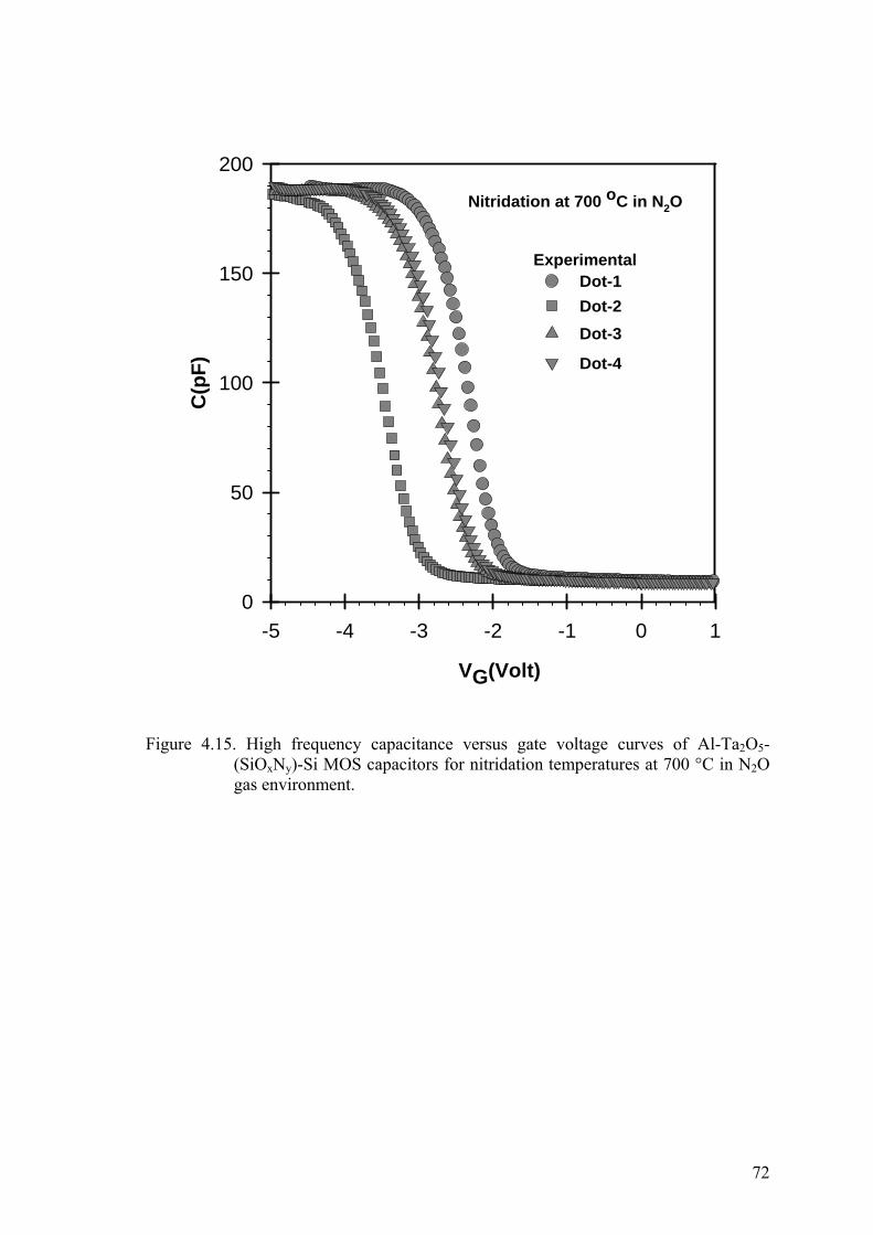
72
Figure 4.15. High frequency capacitance versus gate voltage curves of Al-Ta2O5-(SiOxNy)-Si MOS capacitors for nitridation temperatures at 700 °C in N2O gas environment.
VG(Volt)
-5 -4 -3 -2 -1 0 1
C(p
F)
0
50
100
150
200
Nitridation at 700 oC in N2O
ExperimentalDot-1
Dot-3Dot-2
Dot-4

73
Hysteresis effect in high frequency C-V measurements shows variation among
the samples measured from the same substrate. In Figure 4.16, two different hysteresis
curves were shown for two different dots taken from the same substrate. All samples
exhibit counterclockwise hysteresis, however, the ΔVFB voltage shifts varies between 30
mV and 800 mV among the dots, indicating different mobile trapped charges acting in
different dot. The corresponding positive mobile trap charge for these voltage shifts are
calculated with the help of equation 3.30 as 5.97x1010 cm-2 and 1.52x1012 cm-2,
respectively.
Doping concentration NA and VFB flat band voltage shifts were obtained from
1/C2 versus VG curves shown in Figure 4.17. Even though NA is almost identical for all
samples, the VFB voltage shifts are different for each dot. It indicates that there is a
variation in Neff as well. This is clearly seen as the ideal C-V is calculated for each
sample and presented together with experimental data. In Figure 4.18, both ideal and
experimental C-V curves normalized to oxide capacitance Cox are shown for dot-1
together with high frequency conductance versus gate voltage VG curve. A large shift of
VFB to negative voltage is also consistent with the peak position of conductance curve of
the same sample. Similar consistent agreements have been obtained for other dots
between VFB shift of C-V and conductance curve. However, this sample shows
substantially high conductance values around 330μS even higher than that of reference
sample-2. The density of effective oxide charge, Neff, was calculated using the VFB
voltage shift obtained from ideal and experimental C-V curves. The values of Neff vary
between 3x1012 cm-2 and 5x1012 cm-2 among the dots. The level of Neff is still high,
same as that of reference sample-2. There is no improvement in Neff due to the
nitridation in N2O at 700 oC. However, leakage current characteristic of one of the
samples shown in Figure 4.19 indicates good improvement as compared to reference
sample-1.
The major effect of prior nitridation process is to improve Si-Ta2O5 interface by
forming a few nm SiOxNy layer at the interface. Dit level, calculated from the ψs versus
VG data shown in Figure 4.20 are presented in Figure 4.21. It is a clear indication that
interface quality between silicon and Ta2O5 has been substantially improved and Dit
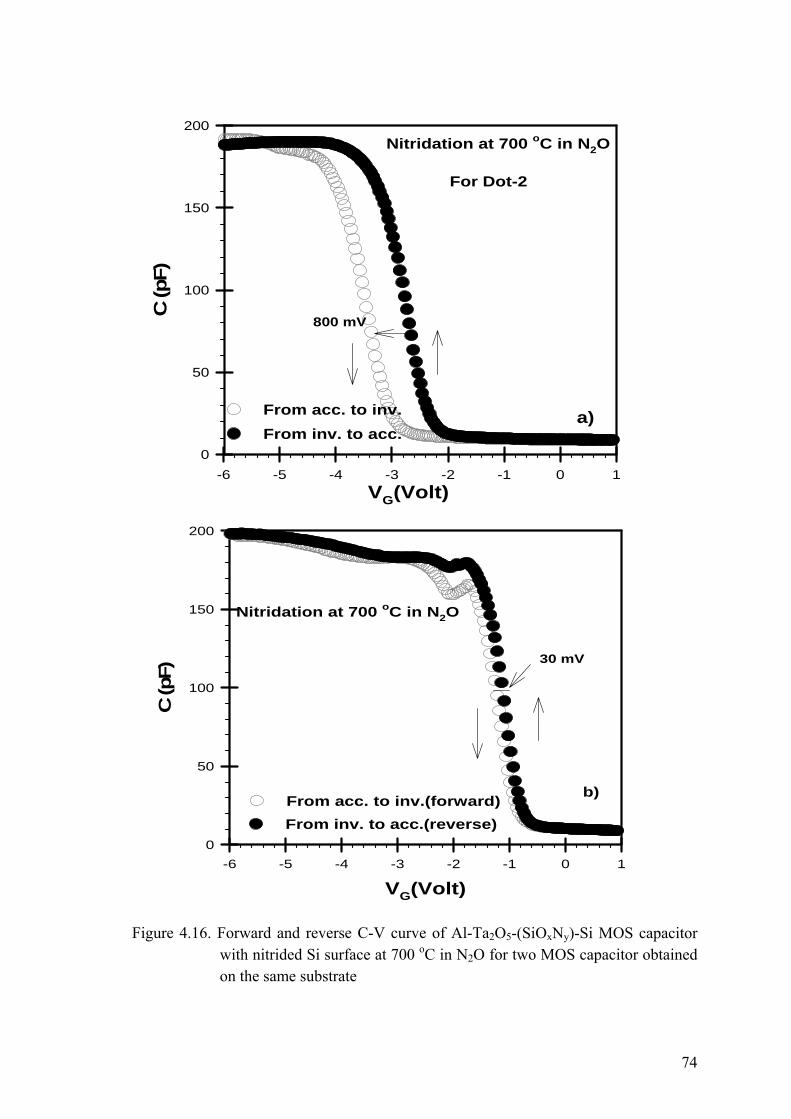
74
Figure 4.16. Forward and reverse C-V curve of Al-Ta2O5-(SiOxNy)-Si MOS capacitor
with nitrided Si surface at 700 oC in N2O for two MOS capacitor obtained on the same substrate
VG(Volt)-6 -5 -4 -3 -2 -1 0 1
C (p
F)
0
50
100
150
200
From acc. to inv.From inv. to acc.
Nitridation at 700 oC in N2O
For Dot-2
a)
800 mV
VG(Volt)-6 -5 -4 -3 -2 -1 0 1
C (p
F)
0
50
100
150
200
From acc. to inv.(forward)From inv. to acc.(reverse)
Nitridation at 700 oC in N2O
b)
30 mV

75
Figure 4.17. Experimental 1/C
2 versus gate voltage VG
graph of four different dots of Al-Ta2O5-(SiOxNy)-Si MOS capacitor for nitridation temperature at 700 °C in N2O gas environment
Figure 4.18. Normalized experimental and theoretical capacitance versus gate voltage
and conductance versus gate voltage of Al-Ta2O5-(SiOxNy)-Si MOS capacitor prepared after nitridation process in N2O at 700ºC.
VG(Volt)-5 -4 -3 -2 -1 0 1
C/C
ox
0.0
0.2
0.4
0.6
0.8
1.0
G(m
icro
S)
0
50
100
150
200
250
300
350
Experimental
Conductance
Theoretical
VFB
VG(Volt)-4 -3 -2 -1 0
1/C2
(cm
2 /F)
x101
5
0
1
2
3
4
5
6
7Nitridation at 700 oC in N2O
Dot-3; N=2.4x1015 cm-3; VFB=-2.4 V
Dot-4; N=3x1015 cm-3; VFB=-2.48 V
Dot-1; N=3x1015 cm-3; VFB=-2.08 V
Dot-2; N=2.4x1015 cm-3; VFB=-3.2 V
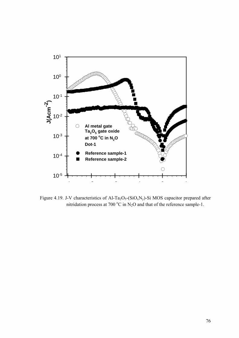
76
Figure 4.19. J-V characteristics of Al-Ta2O5-(SiOxNy)-Si MOS capacitor prepared after
nitridation process at 700 oC in N2O and that of the reference sample-1.
4 3 2 1 0 1
J(A
cm-2
)
10-5
10-4
10-3
10-2
10-1
100
101
Al metal gate Ta2O5 gate oxide at 700 oC in N2ODot-1
Reference sample-1Reference sample-2
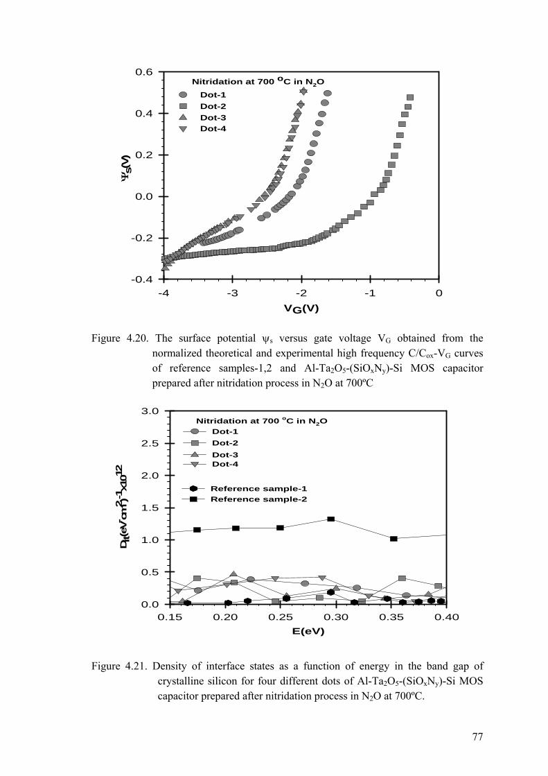
77
Figure 4.20. The surface potential ψs versus gate voltage VG obtained from the normalized theoretical and experimental high frequency C/Cox-VG curves of reference samples-1,2 and Al-Ta2O5-(SiOxNy)-Si MOS capacitor prepared after nitridation process in N2O at 700ºC
Figure 4.21. Density of interface states as a function of energy in the band gap of
crystalline silicon for four different dots of Al-Ta2O5-(SiOxNy)-Si MOS capacitor prepared after nitridation process in N2O at 700ºC.
VG(V)-4 -3 -2 -1 0
-0.4
-0.2
0.0
0.2
0.4
0.6
Dot-1
Dot-3Ψ
s(V)
Dot-4
Dot-2
Nitridation at 700 oC in N2O
E(eV)0.15 0.20 0.25 0.30 0.35 0.40
Dit(
eV- c
m2 )
-1x1
012
0.0
0.5
1.0
1.5
2.0
2.5
3.0
Dot-3Dot-4
Dot-1Dot-2
Reference sample-1
Nitridation at 700 oC in N2O
Reference sample-2

78
level decreased to the levels of reference sample-1 and reach the value of 3±1x10¹¹
(eVcm2)-1 as summarized in Table 4.3. Dit level was an order of magnitude higher for
reference sample-2, with Ta2O5 oxide layer formed on unnitrided silicon surface.
Table 4.3. Summary of parameter extracted from experimental high frequency C-V
measurements of Al-Ta2O5-(SiOxNy)-Si MOS capacitor prepared after nitridation process at 700 oC in N2O gas ambient
It was shown that nitridation of Si surface in N2O gas ambient at 700ºC has
greatly improved the interface quality between silicon and Ta2O5 insulating layer.
Nitridation in N2O gas have also been carried out at 800ºC and 850ºC. For both process
temperature, the results of four different dots from the same substrate show almost
identical oxide capacitance values as shown in Figure 4. 22. For nitridation process at
800ºC, dielectric constant obtained from oxide capacitance measured at accumulation is
almost the same as that found for nitridation process at 700ºC, which is around 6.5.
However it increases to 10.2 for nitridation process carried out at 850ºC. Moreover, the
equivalent oxide thickness teq of SiO2 which gives the same capacitance values are
obtained to be 11 nm for nitridation process at 800ºC, while 7.6 nm for nitridation
process at 850ºC.
Hysteresis behaviors of the samples were also measured. It was found that
hysteresis behavior of the high frequency C-V curve is 700 mV for 800ºC sample and
600 mV for 850 º C sample as shown in Figure 4.23. Both of them indicate
counterclockwise hysteresis, which is the result of a voltage shift towards negative
voltages. These voltage shifts are similar to those found for the samples of nitridation
Dot tox (nm)
S (cm2) k Cox
(pF)
Na (cm-3) x1015
VFB (slope) (volt)
VFB (shift) (volt)
teq (nm)
Neff x1011 (cm-2)
Dit x1011
(eVcm2)-1
Dot-1 6.9 190 -2.4 -2.08 -2.1 11.3 32 3± 1
Dot-2 6.9 189 -2.4 -3.2 -3.3 11.4 50 3± 1
Dot-3 6.7 187 -2.4 -2.4 -2.6 11.5 29 2± 2
Dot-4
20 6.25 x10⁻⁴
6.9 190 -3 -2.5 -2.5 11.3 32 3± 1
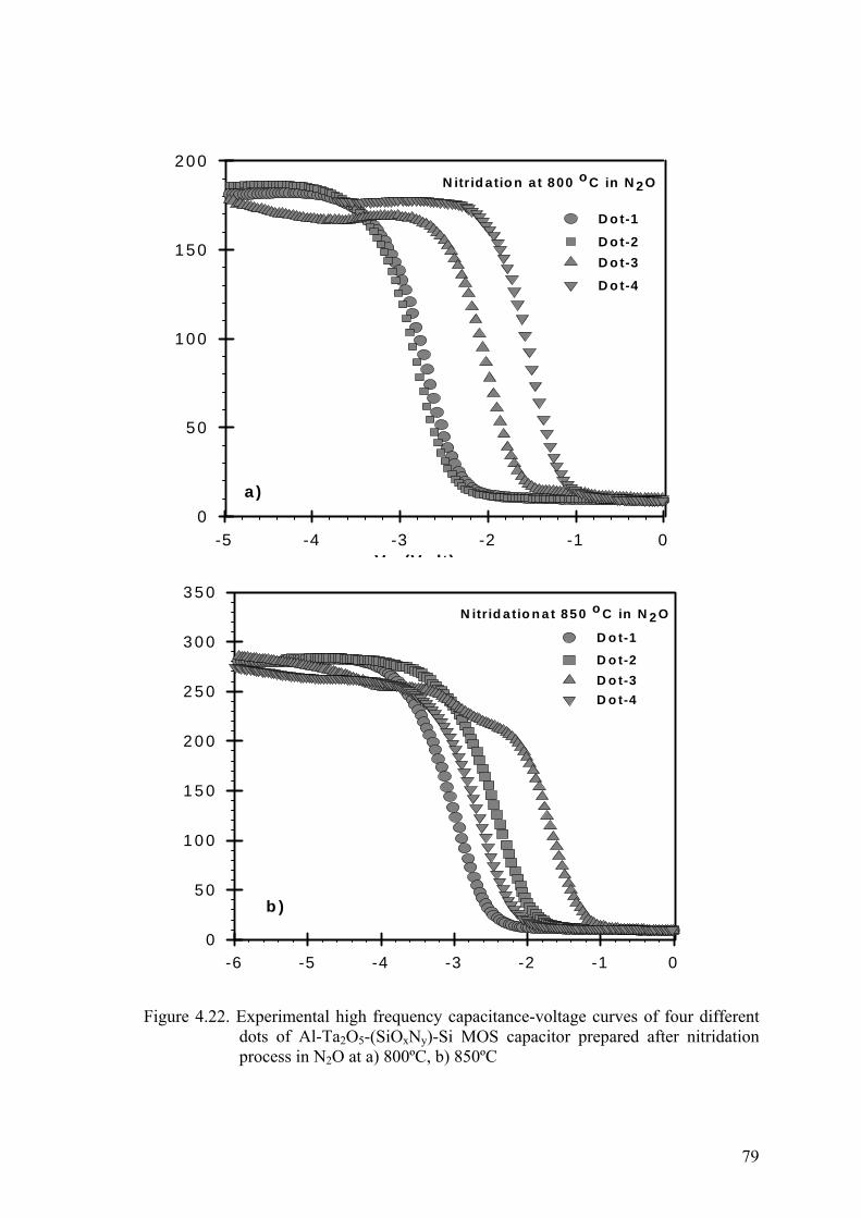
79
Figure 4.22. Experimental high frequency capacitance-voltage curves of four different dots of Al-Ta2O5-(SiOxNy)-Si MOS capacitor prepared after nitridation process in N2O at a) 800ºC, b) 850ºC
( )
-6 -5 -4 -3 -2 -1 00
5 0
1 0 0
1 5 0
2 0 0
2 5 0
3 0 0
3 5 0N itr id a tio n a t 8 5 0 o C in N 2 O
D o t-1
D o t-2D o t-3D o t-4
b )
V (V lt)-5 -4 -3 -2 -1 0
(p)
0
50
100
150
200N itrid atio n a t 800 o C in N 2O
D o t-1
D o t-2D o t-3
D o t-4
a )
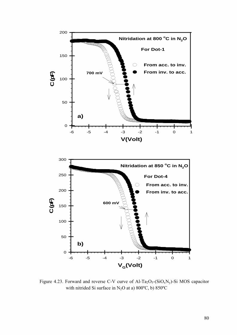
80
Figure 4.23. Forward and reverse C-V curve of Al-Ta2O5-(SiOxNy)-Si MOS capacitor with nitrided Si surface in N2O at a) 800ºC, b) 850ºC
V(Volt)-6 -5 -4 -3 -2 -1 0 1
C (p
F)
0
50
100
150
200
From acc. to inv.
From inv. to acc.
Nitridation at 800 oC in N2O For Dot-1
700 mV
a)
VG(Volt)-6 -5 -4 -3 -2 -1 0 1
C (p
F)
0
50
100
150
200
250
300
From acc. to inv.
From inv. to acc.
Nitridation at 850 oC in N2O
For Dot-4
600 mV
b)

81
process at 700ºC. However, they are substantially higher than reference samples1,
reference sample 2 and required levels of good quality high-k oxide layers. The
corresponding positive mobile trap charge density for this voltage shift is calculated
with the help of equation 3.29 as 1.27x1012 cm-2 for 800ºC process temperature and
1.72x1012 cm-2 for 850ºC process temperature, respectively.
Doping concentration NA of silicon substrate and the flat band voltage VFB shifts
were obtained from 1/C2 versus VG curves shown in Figure 4.24 for both process
temperatures. NA of the both samples shows almost identical values for each MOS
capacitor obtained on the same substrate and found to be around -2.4x1015 cm-3 for both
temperature processes. However, the flat band voltage VFB varies for each sample. The
VFB shift of each dot is consistent with that found from the peak position of conductance
versus gate voltage as shown in Figure 4.25 for dot-1 of the sample at 800ºC and dot-3
at 850ºC. Comparing to sample obtained at 700 ºC higher conductance values were
obtained for those samples. Moreover, as the nitridation temperature increased increase
in conductivity of the insulating layer was observed. While maximum conductance
values for the sample at 800 ºC is around 350 μS, it is around 400 μS for the sample at
850 ºC. Effective oxide charge density obtained from the voltage shifts indicate the
levels of (3±2)x1012 cm-2 for both 800ºC and 850ºC nitridation process in N2O gas. This
level of Neff is similar for nitridation at 700ºC and does indicate any improvement from
that found in reference sample-1.
As the leakage currents concerned, for both 800ºC and 850ºC process samples
shows lower leakage current at inversion region as shown in Figure 4.26. However,
leakage current in the depletion region around flat band voltages VFB of each sample are
much higher than that of reference sample-1. This high level of leakage currents at VFB
voltage is consisted with peak value of conductance curve shown in Figure 4.25.
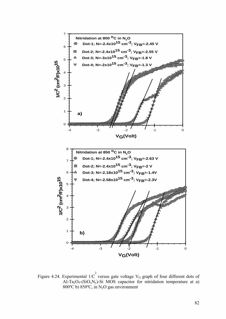
82
Figure 4.24. Experimental 1/C
2 versus gate voltage VG
graph of four different dots of Al-Ta2O5-(SiOxNy)-Si MOS capacitor for nitridation temperature at a) 800ºC b) 850ºC, in N2O gas environment
VG(Volt)-4 -3 -2 -1 0
1/C
2 (c
m2 /
F)x1
015
0
1
2
3
4
5
6
7
8Nitridation at 850 oC in N2O
Dot-3; N=-2.18x1015 cm-3; VFB=-1.4V
Dot-4; N=-2.58x1015 cm-3; VFB=-2.3V
Dot-1; N=-2.4x1015 cm-3; VFB=-2.63 V
Dot-2; N=-2.4x1015 cm-3; VFB=-2 V
b)
VG(Volt)-4 -3 -2 -1 0
1/C
2 (c
m2 /
F)x1
015
0
1
2
3
4
5
6
7Nitridation at 800 oC in N2O
Dot-3; N=-3x1015 cm-3; VFB=-1.8 V
Dot-4; N=-2x1015 cm-3; VFB=-1.3 V
Dot-1; N=-2.4x1015 cm-3; VFB=-2.45 V
Dot-2; N=-2.4x1015 cm-3; VFB=-2.55 V
a)
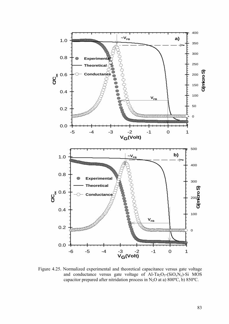
83
Figure 4.25. Normalized experimental and theoretical capacitance versus gate voltage and conductance versus gate voltage of Al-Ta2O5-(SiOxNy)-Si MOS capacitor prepared after nitridation process in N2O at a) 800ºC, b) 850ºC.
VG(Volt)-5 -4 -3 -2 -1 0 1
C/C
ox
0.0
0.2
0.4
0.6
0.8
1.0
G(m
icro
S)
0
50
100
150
200
250
300
350
400
Experimental
Conductance
Theoretical
VFB
~VFB a)
VG(Volt)-6 -5 -4 -3 -2 -1 0 1
C/C
ox
0.0
0.2
0.4
0.6
0.8
1.0
G(m
icro
S)
0
100
200
300
400
500
Experimental
Conductance
Theoretical
VFB
~VFBb)
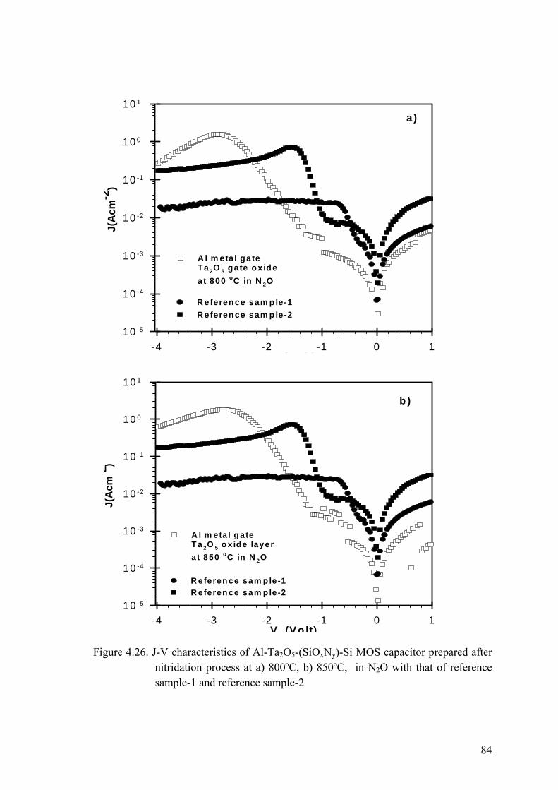
84
Figure 4.26. J-V characteristics of Al-Ta2O5-(SiOxNy)-Si MOS capacitor prepared after
nitridation process at a) 800ºC, b) 850ºC, in N2O with that of reference sample-1 and reference sample-2
V (V o lt)-4 -3 -2 -1 0 1
J(A
cm2 )
10 -5
10 -4
10 -3
10 -2
10 -1
10 0
10 1
A l m eta l g ate T a 2O 5 o x ide layerat 850 oC in N 2O
R eferen ce sam ple-1
b )
R eferen ce sam ple-2
V (V lt)-4 -3 -2 -1 0 1
J(A
cm-2
)
10-5
10 -4
10 -3
10 -2
10 -1
100
101
A l m etal gate Ta2O 5 gate oxide at 800 oC in N 2O
R eference sam ple-1
a)
R eference sam ple-2
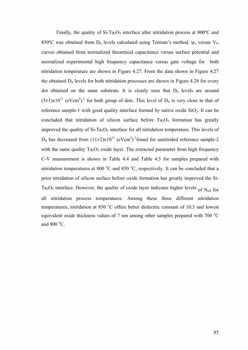
85
Finally, the quality of Si-Ta2O5 interface after nitridation process at 800ºC and
850ºC was obtained from Dit levels calculated using Terman’s method. ψs versus VG
curves obtained from normalized theoretical capacitance versus surface potential and
normalized experimental high frequency capacitance versus gate voltage for both
nitridation temperature are shown in Figure 4.27. From the data shown in Figure 4.27
the obtained Dit levels for both nitridation processes are shown in Figure 4.28 for every
dot obtained on the same substrate. It is clearly seen that Dit levels are around
(3±1)x1011 (eVcm2)-1 for both group of dots. This level of Dit is very close to that of
reference sample-1 with good quality interface formed by native oxide SiO2. It can be
concluded that nitridation of silicon surface before Ta2O5 formation has greatly
improved the quality of Si-Ta2O5 interface for all nitridation temperature. This levels of
Dit has decreased from (11±2)x1011 (eVcm2)-1found for unnitrided reference sample-2
with the same quality Ta2O5 oxide layer. The extracted parameter from high frequency
C-V measurement is shown in Table 4.4 and Table 4.5 for samples prepared with
nitridation temperatures at 800 oC and 850 oC, respectively. It can be concluded that a
prior nitridation of silicon surface before oxide formation has greatly improved the Si-
Ta2O5 interface. However, the quality of oxide layer indicates higher levels of Neff for
all nitridation process temperatures. Among these three different nitridation
temperatures, nitridation at 850 oC offers better dielectric constant of 10.3 and lowest
equivalent oxide thickness values of 7 nm among other samples prepared with 700 oC
and 800 oC.

86
Figure 4.27. The surface potential ψs versus gate voltage VG obtained from the normalized theoretical and experimental high frequency C/Cox vs VG curves of Al-Ta2O5-(SiOxNy)-Si MOS capacitor prepared after nitridation process in N2O at a) 800ºC, b) 850ºC.
VG(V)-4 -3 -2 -1 0
-0.4
-0.2
0.0
0.2
0.4
0.6
Dot-1
Dot-3Ψ
s(V)
Dot-4
Dot-2
Nitridationat 800 oC in N2O
a)
VG(Volt)
-4 -3 -2 -1 0-0.4
-0.2
0.0
0.2
0.4
0.6
Dot-1
Dot-3
Ψs(
V)
Dot-4
Dot-2
Nitridation at 850 oC in N2O
b)
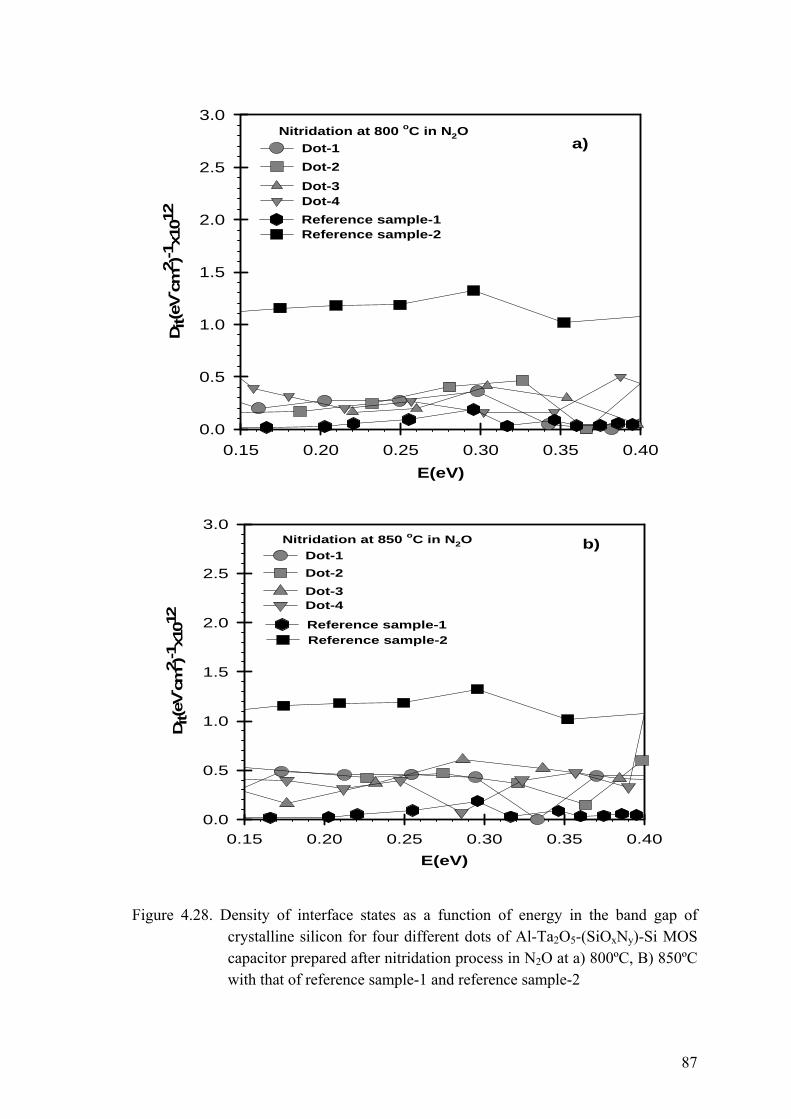
87
Figure 4.28. Density of interface states as a function of energy in the band gap of
crystalline silicon for four different dots of Al-Ta2O5-(SiOxNy)-Si MOS capacitor prepared after nitridation process in N2O at a) 800ºC, B) 850ºC with that of reference sample-1 and reference sample-2
E(eV)0.15 0.20 0.25 0.30 0.35 0.40
Dit(
eV- c
m2 )
-1x1
012
0.0
0.5
1.0
1.5
2.0
2.5
3.0
Dot-3Dot-4
Dot-1Dot-2
Reference sample-1
Nitridation at 800 oC in N2O
Reference sample-2
a)
E(eV)0.15 0.20 0.25 0.30 0.35 0.40
Dit(
eV- c
m2 )
-1x1
012
0.0
0.5
1.0
1.5
2.0
2.5
3.0
Dot-3Dot-4
Dot-1Dot-2
Reference sample-1
Nitridation at 850 oC in N2O
Reference sample-2
b)
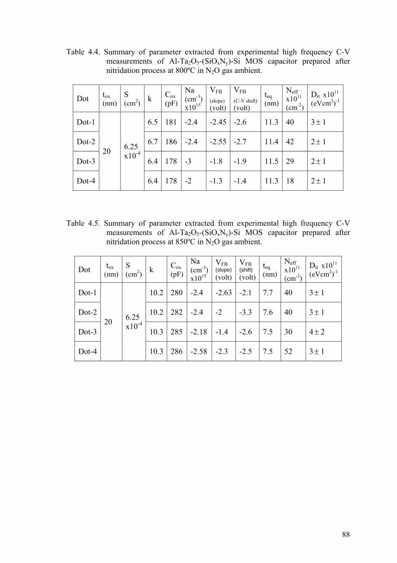
88
Table 4.4. Summary of parameter extracted from experimental high frequency C-V measurements of Al-Ta2O5-(SiOxNy)-Si MOS capacitor prepared after nitridation process at 800ºC in N2O gas ambient.
Table 4.5. Summary of parameter extracted from experimental high frequency C-V measurements of Al-Ta2O5-(SiOxNy)-Si MOS capacitor prepared after nitridation process at 850ºC in N2O gas ambient.
Dot tox (nm)
S (cm2) k Cox
(pF)
Na (cm-3) x1015
VFB
(slope) (volt)
VFB
(C-V shift) (volt)
teq (nm)
Neff x1011
(cm-2)
Dit x1011
(eVcm2)-1
Dot-1 6.5 181 -2.4 -2.45 -2.6 11.3 40 3± 1
Dot-2 6.7 186 -2.4 -2.55 -2.7 11.4 42 2± 1
Dot-3 6.4 178 -3 -1.8 -1.9 11.5 29 2± 1
Dot-4
20 6.25 x10⁻⁴
6.4 178 -2 -1.3 -1.4 11.3 18 2± 1
Dot tox (nm)
S (cm2) k Cox
(pF)
Na (cm-3) x1015
VFB (slope) (volt)
VFB (shift) (volt)
teq (nm)
Neff x1011 (cm-2)
Dit x1011
(eVcm2)-1
Dot-1 10.2 280 -2.4 -2.63 -2.1 7.7 40 3± 1
Dot-2 10.2 282 -2.4 -2 -3.3 7.6 40 3± 1
Dot-3 10.3 285 -2.18 -1.4 -2.6 7.5 30 4± 2
Dot-4
20 6.25 x10⁻⁴
10.3 286 -2.58 -2.3 -2.5 7.5 52 3± 1

89
4.4.2 Prior Nitridation of Silicon Surface in NH3 Gas Ambient
As presented in previous section, nitridation process of silicon surface in N2O
gas prior to oxide formation has greatly improved the Si- Ta2O5 interface quality.
Alternative nitridation process of silicon surface is carried out in NH3 gas environment.
In this thesis, electronic properties of metal-Ta2O5-SiOxNy-Si MOS capacitors were also
investigated using a prior nitridation process of silicon surface in NH3 gas environment
at 700ºC and 800ºC.
High frequency C-V characteristics of MOS capacitors prepared after nitridation
of silicon surface at 700ºC in NH3 gas ambient are presented in Figure 4.29 for four
different dots. It is seen that oxide capacitance at accumulation region shows slight
variation around 335 pF±10 pF. This could be due to a strong interaction between gate
metal and gate oxide Ta2O5, which causes slight differences in oxide thickness and
capacitance values. In addition, oxide capacitance in accumulation region shows two
step changes. These steps can be explained by trapping slow states. Dielectric constant
was calculated for each sample by using oxide capacitance, measured oxide thickness
and gate area of each sample. It is important that dielectric constant around 12 has been
obtained for all samples, which is almost factor of 2 higher than that of samples nitrided
in N2O gas at the same temperature. It is a substantial improvement in dielectric
constant for high-k oxide as compared to nitridation process carried out in N2O gas.
The effects of mobile trap charges in oxide are presented in Figure 4.30 for Dot-
3. Hysteresis effect of high frequency C-V curve shows 700 mV voltage shifts towards
negative voltages. This indicates that positively charged mobile trap charges are present
in Ta2O5 high-k oxide layer. Density of mobile trap charges is comparable to that
observed in MOS capacitors prepared after nitridation process in N2O gas at 700oC. Its
density obtained from the voltage shift is in the range of 2.4x1012 cm-2. Leakage current
density versus gate voltage VG obtained from the simultaneously measured conductance
values is shown in Figure 4.31 for the capacitor presented as dot-3 of Figure 4.29. It is
seen that leakage current density values are lower than that of reference sample-1 and
reference sample-2 in inversion region. However, leakage currents of dot-3 in depletion
region, at gate voltages around the VFB, is higher than measured for reference sample-1
as seen in Figure 4.31.

90
Figure 4.29. Experimental high frequency capacitance versus gate voltage curves of
four different dots of Al-Ta2O5-(SiOxNy)-Si MOS capacitor prepared after nitridation process of silicon surface in NH3 gas environment at 700ºC
Figure 4.30. Forward and reverse C-V curve of Al-Ta2O5-(SiOxNy)-Si MOS capacitor
with nitrided Si surface at 700ºC in NH3
VG(Volt)
-6 -5 -4 -3 -2 -1 0 1
C(p
F)
0
50
100
150
200
250
300
350Nitridation at 700 oC in NH3
Dot-1
Dot-3Dot-2
Dot-4
VG(Volt)-6 -5 -4 -3 -2 -1 0 1
C (p
F)
0
50
100
150
200
250
300
350
From acc. to inv.
From inv. to acc.
Nitridation at 700 oC in NH3
700 mV

91
Figure 4.31. J-V characteristics of Al-Ta2O5-(SiOxNy)-Si MOS capacitor prepared after
nitridation process at 700ºC in NH3 and that of the reference sample-1.
V (Volt)-4 -3 -2 -1 0 1
J(A
cm-2
)
10-6
10-5
10-4
10-3
10-2
10-1
100
101
Nitridation at 700 oC in NH3
Reference sample-1Reference sample-2
Dot-3
92
Complete understanding of the non ideal effects present in MOS capacitors requires
calculation of theoretical capacitance-voltage characteristics. In Figure 4.32, 1/C2 versus
gate voltage VG curves are presented for four different MOS capacitors from the same
substrate. All of the curves indicate identical slope resulting in a homogeneous acceptor
concentration of -2.5x1015 cm-3. However, intercepts of the slopes on the VG axis shows
a large variation from -1.1 V to -2.1 V. It is inferred that density of effective oxide
charges is not uniform in each sample. Using the experimentally derived parameters,
theoretical C-V curves are calculated for each sample and presented together with
experimental high frequency C-V curve. In Figure 4.33, theoretical and experimental C-
V curves normalized to oxide capacitance are shown for Dot-3 together with
conductance values of the same sample. A substantial shift of flat band voltage VFB
from the ideal C-V curve at VG=0 V is almost equal to that found from Figure 4.32
within the experimental error. The value of VFB seen in Figure 4.33 exists almost at the
same VG value of conductance peak as expected. However the extracted conductance
values of the samples are higher than that of the samples nitrided in N2O and reach the
value of 500 μS which is very high for insulating properties. Using the VFB voltage shift
of each sample, effective oxide charge density, Neff, of each sample were calculated
using equation 3.29. The results of Neff are given in Table 4.6. It is seen that the values
of Neff are almost similar to those found in nitrided samples in N2O gas environment and
much higher than the reference sample-1.
Finally the most important non ideal effect seen in MOS capacitors, the quality
of Si-Ta2O5 interface was investigated. In Figure 4.34, surface potential ψs versus gate
voltage VG curves of four different MOS capacitors prepared after nitridation process in
NH3 at 700ºC are shown. Interface trap density Dit levels of samples were calculated
using Terman’s method and shown in Figure 4.35 together with those of reference
samples. Dit levels are much lower than that of unnitrided reference sample-2 and closer
to that of reference sample-1. Dit levels show variation around (4±3)x1011 (eVcm2)-1,
which are slightly higher than those found for MOS capacitors of nitridation in N2O at
700ºC. It can be inferred that nitridation process in N2O gas forms better interface
between silicon and Ta2O5 oxide layer due to reach oxygen in N2O.

93
Figure 4.32. Experimental 1/C
2 versus gate voltage VG
graph of four different dots of Al-Ta2O5-(SiOxNy)-Si MOS capacitor for nitridation temperature at 700ºC in NH3 gas environment
Figure 4.33. Conductance, G versus gate voltage and theoretical and experimental
normalized high frequency capacitance-voltage curves of Al-Ta2O5-(SiOxNy)-Si MOS capacitor prepared after nitridation process in NH3 at 700ºC.
VG(Volt)
-3 -2 -1 0 1
1/C2
(cm
2 /F)
x101
5
0
1
2
3
4
5
6
7Nitridation at 700 oC in NH3
Dot-3; N=-2.4x1015 cm-3; VFB=-2.1 V
Dot-4; N=-2.4x1015 cm-3; VFB=-1.6V
Dot-1; N=-2.29x1015 cm-3; VFB=-1.1 V
Dot-2; N=-2.42x1015 cm-3; VFB=-1.8 V
VG(Volt)
-6 -5 -4 -3 -2 -1 0 1
C/C
ox
0.0
0.2
0.4
0.6
0.8
1.0
G(m
icro
S)
0
100
200
300
400
500
600
ExperimentalTheoretical
VFB
Conductance
~VFBNitridation at 700 oC in NH3
Sample: Dot-3

94
Table 4.6. Summary of parameter extracted from experimental high frequency C-V measurements of Al-Ta2O5-(SiOxNy)-Si MOS capacitor prepared after nitridation process at 700ºC in NH3 gas ambient
Figure 4.34. The surface potential ψs versus gate voltage VG obtained from the
normalized theoretical and experimental high frequency C/Cox curves of Al-Ta2O5-(SiOxNy)-Si MOS capacitor prepared after nitridation process in NH3 at 700ºC
Dot tox (nm)
S (cm2) k Cox
(pF)
Na (cm-3) x1015
VFB (slope) (volt)
VFB (shift) (volt)
teq (nm)
Neff x1011 (cm-2)
Dit x1011
(eVcm2)-1
Dot-1 11.9 327 -2.3 -1.1 -1.2 6.2 29 6± 1
Dot-2 12.5 345 -2.4 -1.8 -2.1 6.2 51 4± 2
Dot-3 12.3 343 -2.4 -2.1 -2.3 6.2 61 4± 3
Dot-4
20 6.25 x10⁻⁴
11.5 318 -2.4 -1.6 -1.7 6.7 38 5± 2
VG(V)-4 -3 -2 -1 0
-0.4
-0.2
0.0
0.2
0.4
0.6
Dot-1
Dot-3
Ψs(
V)
Dot-4
Dot-2
Nitridation at 700 oC in NH3
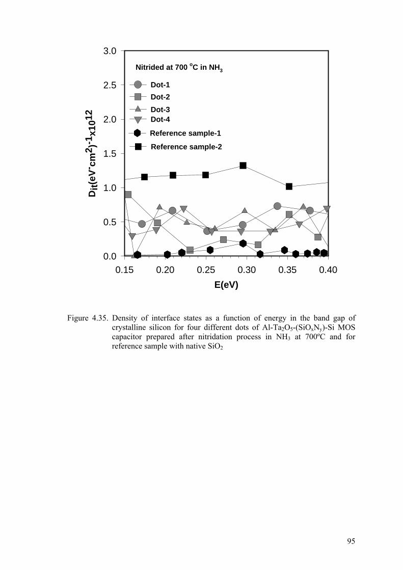
95
Figure 4.35. Density of interface states as a function of energy in the band gap of
crystalline silicon for four different dots of Al-Ta2O5-(SiOxNy)-Si MOS capacitor prepared after nitridation process in NH3 at 700ºC and for reference sample with native SiO2
E(eV)0.15 0.20 0.25 0.30 0.35 0.40
Dit(
eV- c
m2 )
-1x1
012
0.0
0.5
1.0
1.5
2.0
2.5
3.0
Dot-3Dot-4
Dot-1Dot-2
Reference sample-1
Nitrided at 700 oC in NH3
Reference sample-2

96
The last nitridation process was carried out at 800ºC in NH3 gas. Experimental
C-V curves of four different dots are shown in Figure 4.36. The oxide capacitance in
accumulation region is 225 pF ± 5 pF for different dots. Dielectric constant derived
from the oxide capacitance is around 8±0.4, which is lower than nitridation at 700ºC in
the same gas ambient. The hysteresis effect on high frequency C-V curve of Dot-2 is
presented in Figure 4.37. There is a counterclockwise behavior similarly obtained in
other nitrided sample. The flat band voltage shift, ΔVFB, is 800 mV indicating high level
of mobile trap charges present in high-k Ta2O5 oxide layer. The positive mobile trap
charge density corresponding to this voltage shift is equal to 1.8x1012 cm-2. This is a
serious non-ideal effect present in all high-k dielectrics and is necessary to be reduced to
the level of native oxide SiO2. On the other hand, leakage current characteristic of Dot-2
is shown in Figure 4.38. It is clearly seen that, the level of leakage current decreases to
the level of reference sample-1 in inversion region. However, the leakage current
density in depletion region at gate voltage around flat band voltage VFB is almost two
orders of magnitude higher than that of reference sample-1.
In order to investigate the effect of other non-ideal effect present in the Ta2O5 oxide
layer and Ta2O5-Si interface, theoretical C-V characteristics are required to be
calculated using the experimentally derived parameters. Doping concentration of p-type
silicon substrate is calculated from the slope of 1/C2 versus VG curves of the samples as
shown in Figure 4.39. In addition, the intercept of the slope on VG axis gives estimated
flat-band voltage shift of C-V curves from the ideal C-V one. This is presented in
Figure 4.40, where both experimental and theoretical capacitance values normalized to
the oxide capacitance show a significant shift along the voltage axis VG. It is clearly
seen that there is a large flat band voltage shift indicating large density of effective
oxide charge. For each sample, similar curves were calculated and reliable VFB voltage
shift were extracted. These flat band values are very close to those found from the
intercept of the slope of 1/C2 vs VG curves. In addition, the VFB values were also
confirmed by the peak position of conductance versus VG, which exist around VFB value
on G versus VG curve. In Figure 4.40, conductance versus VG curve of the same sample
is also shown, where peak position of G versus VG is around VFB voltage shift of
experimental C-V curve. The obtained conductance values for these samples are in the
same range as the previous sample.
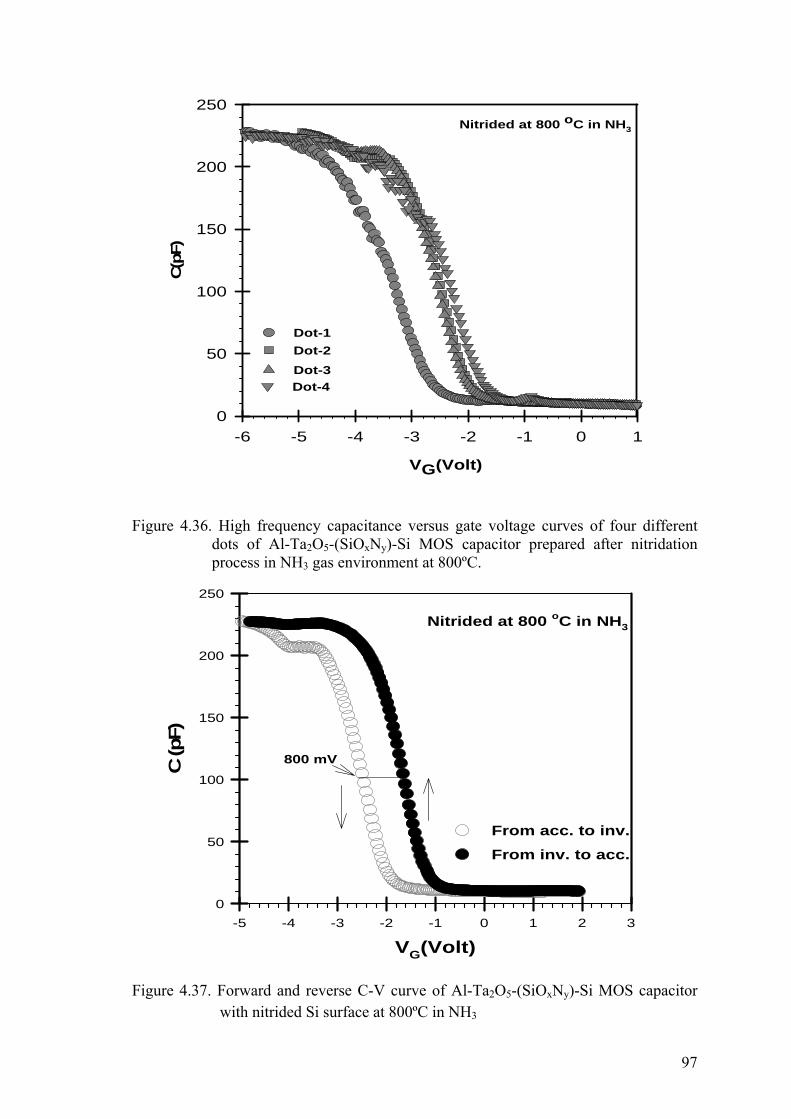
97
Figure 4.36. High frequency capacitance versus gate voltage curves of four different dots of Al-Ta2O5-(SiOxNy)-Si MOS capacitor prepared after nitridation process in NH3 gas environment at 800ºC.
Figure 4.37. Forward and reverse C-V curve of Al-Ta2O5-(SiOxNy)-Si MOS capacitor with nitrided Si surface at 800ºC in NH3
VG(Volt)-5 -4 -3 -2 -1 0 1 2 3
C (p
F)
0
50
100
150
200
250
From acc. to inv.
From inv. to acc.
Nitrided at 800 oC in NH3
800 mV
VG(Volt)
-6 -5 -4 -3 -2 -1 0 1
C(p
F)
0
50
100
150
200
250Nitrided at 800 oC in NH3
Dot-1
Dot-3Dot-2
Dot-4

98
Figure 4.38. J-V characteristics of Al-Ta2O5-(SiOxNy)-Si MOS capacitor prepared after
nitridation process at 800ºC in NH3 and that of the reference sample-1.
Figure 4.39. Experimental 1/C
2 versus gate voltage VG
graph of four different dots of Al-Ta2O5-(SiOxNy)-Si MOS capacitor for nitridation temperature at 800ºC in NH3 gas environment
VG(Volt)-4 -3 -2 -1 0
1/C2
(cm
2 /F)
x101
5
0
1
2
3
4
5
6
7Nitrided at 800 oC in NH3
Dot-3; N=3.3x1015 cm-3; VFB=-2.18 V
Dot-1; N=3.7x1015 cm-3; VFB=-2.8 V
Dot-2; N=-3x1015 cm-3; VFB=-2.18 V
Dot-4; N=3x1015 cm-3; VFB=-1.9 V
VG(Volt)-3 -2 -1 0 1
J(Acm
-2)
10-5
10-4
10-3
10-2
10-1
100
Dot-2Reference sample-1Reference sample-2
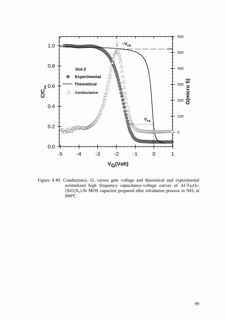
99
Figure 4.40. Conductance, G, versus gate voltage and theoretical and experimental
normalized high frequency capacitance-voltage curves of Al-Ta2O5-(SiOxNy)-Si MOS capacitor prepared after nitridation process in NH3 at 800ºC.
VG(Volt)
-5 -4 -3 -2 -1 0 1
C/C
ox
0.0
0.2
0.4
0.6
0.8
1.0
G(m
icro
S)
0
100
200
300
400
500
600
Experimental
Theoretical
VFB
Conductance
~VFB
Dot-2

100
The values of extracted VFB are used to calculate the Neff of each MOS capacitor
taken from the same substrate. The VFB values show a variation from -2,3 to -3.4 volt
among the samples. Correspondingly, the calculated Neff values show variation between
3.5x1012 cm-2 and 5.7x1012 cm-2 as summarized in Table 4.7. These levels are quite high
for an oxide to be used in as a replacement of native oxide SiO2.
Furthermore, the density of interface traps are calculated for the samples using
ψs versus VG curves shown in Figure 4.41 and procedure of Terman’s Method. The
resulting Dit levels of nitrided samples in NH3 at 800 OC and that of reference samples
are presented in Figure 4.42. The levels of Dit show a variation among the samples. It is
around 5±3x10¹¹ (eVcm2)-1, which is quite higher than that of reference sample-1.
However it is substantially lower than that of unnitrided reference sample-2 with high-k
dielectric. Additional research is required to improve the Dit level by improving Ta2O5-
Si interface.
Table 4.7. Summary of parameter extracted from experimental high frequency C-V
measurements of Al-Ta2O5-(SiOxNy)-Si MOS capacitor prepared after nitridation process at 800ºC in NH3 gas ambient.
Dot tox (nm)
S (cm2) k Cox
(pF)
Na (cm-3) x1015
VFB (slope) (volt)
VFB (shift) (volt)
teq (nm)
Neff x1011 (cm-2)
Dit x1011
(eVcm2)-1
Dot-1 8.3 228 -3.6 -2.8 -3 9.4 57 7± 3
Dot-2 7.6 227 -3 -2.18 -2.3 9.4 42 6± 2
Dot-3 8.4 232 -3.3 -2.18 -2.3 9.5 42 4± 3
Dot-4
20 6.25 x10⁻⁴
8.1 224 -3 -1.9 -2 9.6 35 5± 3
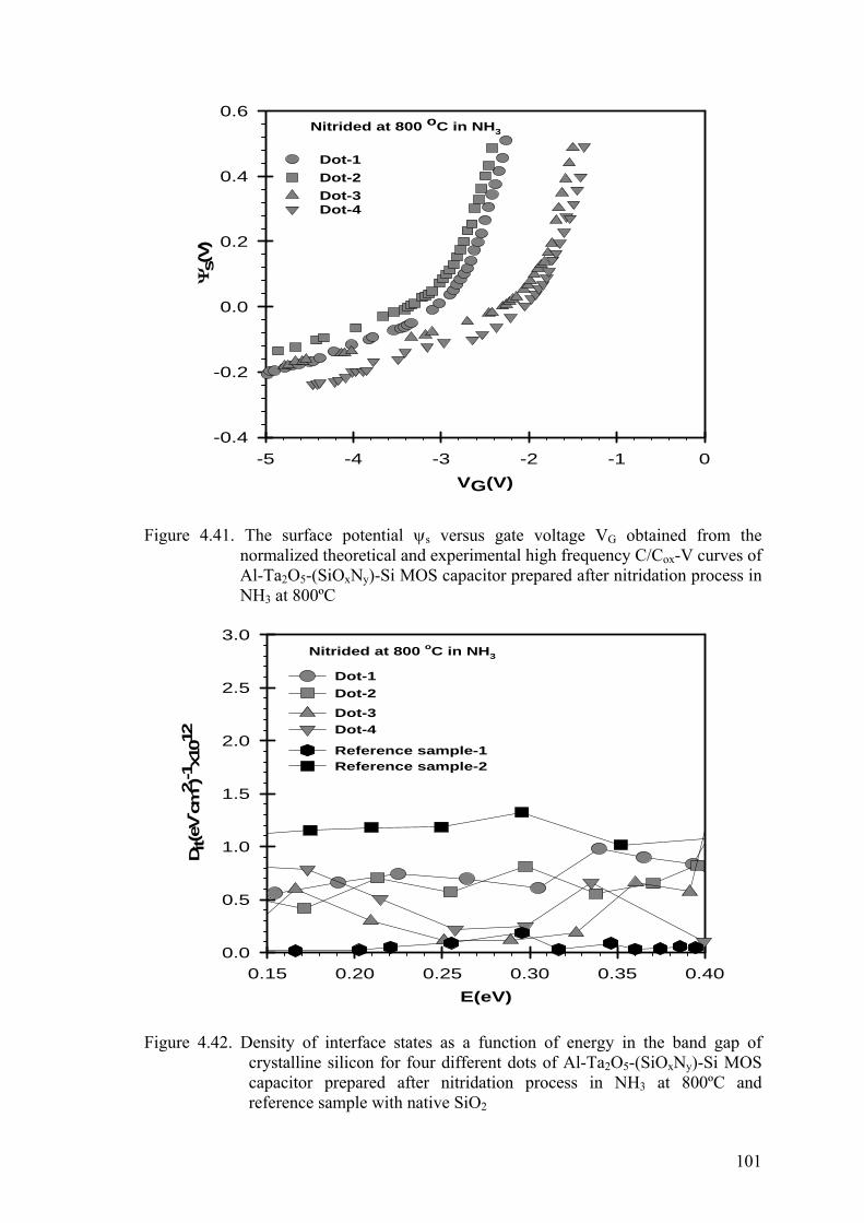
101
Figure 4.41. The surface potential ψs versus gate voltage VG obtained from the normalized theoretical and experimental high frequency C/Cox-V curves of Al-Ta2O5-(SiOxNy)-Si MOS capacitor prepared after nitridation process in NH3 at 800ºC
Figure 4.42. Density of interface states as a function of energy in the band gap of
crystalline silicon for four different dots of Al-Ta2O5-(SiOxNy)-Si MOS capacitor prepared after nitridation process in NH3 at 800ºC and reference sample with native SiO2
VG(V)-5 -4 -3 -2 -1 0
-0.4
-0.2
0.0
0.2
0.4
0.6
Dot-1
Dot-3Ψ
s(V)
Dot-2
Nitrided at 800 oC in NH3
Dot-4
E(eV)0.15 0.20 0.25 0.30 0.35 0.40
Dit(
eV- c
m2 )
-1x1
012
0.0
0.5
1.0
1.5
2.0
2.5
3.0
Dot-3
Dot-1Dot-2
Reference sample-1
Nitrided at 800 oC in NH3
Dot-4
Reference sample-2
102
4.4.3 Conclusions
In this part of thesis, the first objective of thesis has been investigated using
MOS capacitors with high-k Ta2O5 oxide layers and two reference samples. First group
of samples was Al- (SiO2)-Si MOS capacitor, as a reference sample-1. Second group of
sample was Al-Ta2O5-(SiO2)-Si MOS capacitor as reference sample-2. The last group of
the samples was Al-Ta2O5-(SiOxNy)-Si MOS capacitor, which was exposed to prior
nitridation process in N2O and NH3 gas ambient before formation of oxide layers.
Analysis of high frequency C-V characteristics of Reference Sample 1 indicated
that native oxide SiO2 has the lowest moving trap charges with ΔVFB less than 30 mV.
The oxide capacitance for the predetermined gate area and oxide thickness resulted in
the dielectric constant of 3.9 as found in the literature. The leakage current density in
the depletion is around ~10-2 Acm-2 and conductance peak value was found to be 22 μS.
The effective oxide charge density Neff is around 2.9x1011 cm-2, and the interface trap
charge density is found to be 2±1x10¹¹(eVcm2)-1. Both Terman’s and simultaneous C-V
method resulted in similar values.
In Reference Sample 2, replacement of SiO2 with high-k Ta2O5 oxide layer
increases the dielectric constant a factor of three. Due to thermal oxidation of Ta films
on silicon ( a smooth process), the level of moving trap charges is still as low as that
observed in native oxide SiO2. However, leakage current, effective oxide charges and
density of interface trap states increase drastically. The peak values of conductance
increased by several times and reach to the value of 90 μS and the leakage current reach
to 1 Acm-2. Due to such high leakage currents observed in high-k dielectrics, low
frequency C-V measurement could not be carried out. Similarly, the effective oxide
charge density increased to 3.2x1012 cm-2 which caused high flat band voltage shift in
the experimental C-V curves. Interface quality between silicon and high-k Ta2O5
worsens and Dit level increases to the values of 1.1±2x10¹² (eVcm2)-1.
In order to improve the interface quality of Si-Ta2O5, a novel approach known as
prior nitridation of silicon surface before formation of Ta2O5 oxide layer was applied in
N2O and NH3 gas ambients at different nitridation temperatures. For the samples
nitrided in N2O, the most promising dielectric constants and equivalent oxide
thicknesses, which are around 10.2 and 7.5 nm, respectively, were obtained for the
samples nitrided at 850 oC. Among the samples nitrided in NH3, the best dielectric
103
constants and equivalent oxide thicknesses were obtained for the sample nitrided at 700 oC as 12 and 6.2 nm, respectively. In both nitridation processes, no improvement in
leakage current levels was observed. Both the conductance and effective oxide charge
density increased several times. On the other hand, among the nitrided samples,
nitridation in N2O provide lower conductance and effective oxide charge values which
are around 350 μS and 30-50x1011 cm-2, respectively. For the samples nitrided in NH3
these characteristics were obtained as 500-600 μS and 30-60x1011 cm-2, respectively.
The most important benefit of the nitridation process is the improvement in density of
interface trap states. For the samples nitrided in N2O, Dit level decreased to the level of
Reference Sample 1 with native oxide SiO2. It decreases from 1.1±2x10¹² (eVcm2)-1 to
the levels of 3±1x10¹¹ (eVcm2)-1. For the case of NH3 nitridation, the levels of Dit
improves from the unnitrided Reference Sample 2, however, slightly higher values were
obtained as compared to N2O nitrided samples.
4.5 The Effects of Metal Gates in MOS Characteristics
A wide variety of metal gates are currently being evaluated as replacements for
n+ and p+ poly silicon gate on high dielectric constant gate dielectrics in CMOS circuit
since they would eliminate the problems of dopant penetration and poly-silicon
depletion currently seen in poly-Si gates due to their high carrier density. Therefore,
understanding the metal gate electrode - gate dielectric interface is critical in device
performance. In this study, the effect of three metal gate electrodes has been
investigated in contact with Ta2O5 gate dielectric. In this part of thesis, four groups of
samples are used. First group has the structure of Al metal gate- Ta2O5(SiO2)-Si MOS
capacitor, where Ta2O5 oxide layer is formed by thermal evaporation of reactively
sputtered Ta films on silicon substrate. Second group of sample have the structure of Al
metal gate-Ta2O5-(SiOxNy)-Si MOS capacitor, where a prior nitridation of silicon
surface in N2O has been carried out before Ta2O5 oxide formation. Oxide layer is
deposited using RF sputtering from Ta target in Ar and O2 gas. Finally Al metal gates
were evaporated on Ta2O5 oxide layer. The third group of samples has the form of TiN
metal gate-Ta2O5(SiO2)-Si MOS capacitor. Here, Ta2O5 oxide layer is formed using
thermal oxidation of reactively sputtered Ta metal films on silicon surface and TiN
104
metal gate was deposited using RF magnetron sputtering on Ta2O5 oxide layer. The
fourth group of samples has W metal gate and has the structure of W metal gate-Ta2O5-
(SiOxNy)-Si MOS capacitor. In this group, a prior nitridation of Si surface in N2O at 700 oC and 850 oC using RTN process was applied before Ta2O5 formation. Oxide layer was
deposited using RF magnetron sputtering from Ta target in Ar and O2 gas mixture. High
frequency C-V spectroscopy has been used to obtain the C-V characteristics of the
samples. Important device parameters such as doping concentration, flat band voltage,
dielectric constant, effective oxide charge and density of interface trap states were
derived and the results were compared with the results of the Al-SiO2-Si MOS
capacitors, reference sample-1.
4.5.1 Results of Al Metal Gate MOS Capacitor
In this section, Al metal gate was used in two different groups of samples; the
first one is the reference sample-2 and the second group is the nitrided samples in N2O
at 700 oC and 850 oC. The results of these two groups of samples were already
presented at the beginning of their chapter. However, they will be summarized in this
part of thesis in order to compare these results with those of other MOS capacitors
having gate metal of TiN and W.
In Figure 4.43, example of high frequency C-V curves of MOS capacitors with
aluminum gate metal are presented for each sample. The results of only one
characteristics dot from each substrate was taken for the representation. Main
differences among the Al gate metal of these MOS capacitors are the effect of prior
surface nitridation process of silicon surface. It is seen that the oxide capacitance and
corresponding dielectric constant is the highest for Al-Ta2O5(SiO2)-Si unnitrided
capacitor. Thermal oxidation of Ta2O5 gives better quality oxide layer. In addition,
hysteresis behavior of the Al metal gate samples are summarized in Figure 4.44, where
Al-Ta2O5(SiO2)-Si unnitrided sample shows almost insignificant ΔVFB voltage shift in
hysteresis of high frequency C-V curve. However, other Al-Ta2O5-SiOxNy-Si MOS
capacitors with a prior nitridation of silicon surface indicate higher ΔVFB voltage shifts
up to 800 mV among different dots taken from the substrate. It can be concluded that
the mobile trap charges are almost insignificant in thermally grown Ta2O5 of reference

105
Figure 4.43. High frequency capacitance versus gate voltage curves of MOS capacitor
with Al metal gates
VG(Volt)
-5 -4 -3 -2 -1 0 1
C(p
F)
0
50
100
150
200
250
300
Al-Ta2O2-SiOxNy-Si
(nitrided at 700 oC)
Al-Ta2O2-(SiO2)-Si(unnitrided)
Al-Ta2O2-SiOxNy-Si
(nitrided at 850 oC)
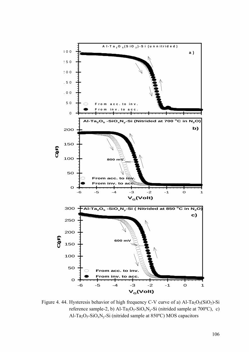
106
Figure 4. 44. Hysteresis behavior of high frequency C-V curve of a) Al-Ta2O5(SiO2)-Si
reference sample-2, b) Al-Ta2O5-SiOxNy-Si (nitrided sample at 700ºC), c) Al-Ta2O5-SiOxNy-Si (nitrided sample at 850ºC) MOS capacitors
0
5 0
1 0 0
1 5 0
2 0 0
2 5 0
3 0 0
F r o m a c c . t o i n v .
F r o m i n v . t o a c c .
a )A l - T a 2 O 5 ( S i O 2 ) - S i ( u n n i t r i d e d )
VG(Volt)-6 -5 -4 -3 -2 -1 0 1
C (p
F)
0
50
100
150
200
250
300
From acc. to inv.
From inv. to acc.
Al-Ta2O5 -SiOxNy-Si ( Nitrided at 850 oC in N2O)
600 mV
c)
VG(Volt)-6 -5 -4 -3 -2 -1 0 1
C (p
F)
0
50
100
150
200
From acc. to inv.From inv. to acc.
Al-Ta2O5 -SiOxNy-Si (Nitrided at 700 oC in N2O)
b)
800 mV

107
sample-2, however their density is substantially higher for Ta2O5 oxide layers prepared
with RF magnetron sputtering on the nitrided silicon surface in N2O gas. The leakage
currents of Al metal gate MOS capacitor are summarized in Figure 4.45. Even though
lower leakage currents are measured in inversion region of MOS capacitors, much
higher leakage currents are obtained in depletion region for reference sample-2 and
nitrided samples in N2O than that of reference sample-1 with Al-SiO2-Si structure. Such
high level of leakage currents are unavoidable feature of high-k oxide layers
independent of processing method used in MOS processing.
Finally, the interface quality of Ta2O5-Si structure is summarized in Figure 4.46
for Al metal gate samples. Dit level is high for thermally grown Ta2O5 on silicon
surface, where not well defined interface with defects occurs. However, Dit levels of Al-
Ta2O5-SiOxNy-Si MOS capacitors prepared after nitridation process of silicon surface in
N2O gas at 700 oC and 850 oC are very close to the level of Al-SiO2-Si reference smple-
1. It is inferred that prior nitridation process of silicon surface before oxide formation is
a promising method to improve the interface quality of Ta2O5-Si structure.
Furthermore, summary of results obtained from the analysis of high frequency
C-V curve of Al metal gate MOS capacitors are presented in Figure 4.8. Even though
there is in Dit levels, the effective oxide charges are substantially high in all MOS
capacitors with Ta2O5 oxide layers. The Neff values are one order of magnitude higher
than that of reference sample-1. But the lowest density of mobile trap charges is present
in thermally grown Ta2O5 layers in reference sample-2.

108
Figure 4.45. J-V characteristics of unnitrided reference sample-2, reference sample-1 and samples prepared after nitridation process at 700 and 850ºC in N2O
Figure 4.46. Density of interface states as a function of energy in the band gap of
crystalline silicon for reference sample-1, unnitrided reference sample-2 and samples prepared after nitridation process at 700 and 850ºC in N2O
E(eV)0.15 0.20 0.25 0.30 0.35 0.40
Dit(
eV- c
m2 )
-1x1
012
0.0
0.5
1.0
1.5
2.0
2.5
3.0Al-Ta2O5-SiOxNy-Si (Nitrided at 700 oC)
Al-SiO2-Si (Reference sample-1)
Al-Ta2O5(SiO2)-Si (Reference sample-2)
Al-Ta2O5-SiOxNy-Si (Nitrided at 850 oC)
-4 -3 -2 -1 0 1
J(A
cm-2
)
1 0 -5
1 0 -4
1 0 -3
1 0 -2
1 0 -1
1 0 0
1 0 1
A l-T a 2O 5-S iO xN y-S i (N itrid e d a t 7 0 0 o C )
A l-T a 2O 5-S iO xN y-S i (N itrid e d a t 8 5 0 o C )
A l-T a 2O 5(S iO 2)-S i (R e fe ren c e sa m p le -2 )A l-S iO 2-S i (R e fe re n c e s a m p le -1 )
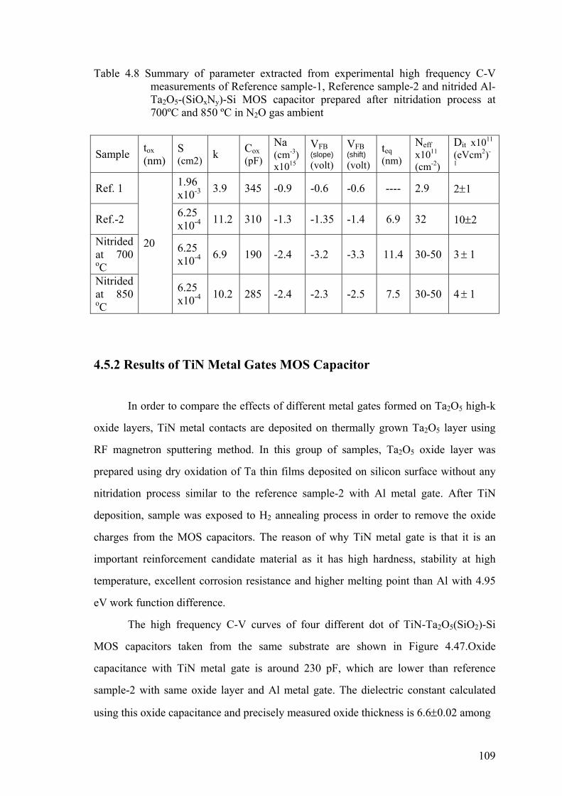
109
Table 4.8 Summary of parameter extracted from experimental high frequency C-V measurements of Reference sample-1, Reference sample-2 and nitrided Al-Ta2O5-(SiOxNy)-Si MOS capacitor prepared after nitridation process at 700ºC and 850 ºC in N2O gas ambient
4.5.2 Results of TiN Metal Gates MOS Capacitor
In order to compare the effects of different metal gates formed on Ta2O5 high-k
oxide layers, TiN metal contacts are deposited on thermally grown Ta2O5 layer using
RF magnetron sputtering method. In this group of samples, Ta2O5 oxide layer was
prepared using dry oxidation of Ta thin films deposited on silicon surface without any
nitridation process similar to the reference sample-2 with Al metal gate. After TiN
deposition, sample was exposed to H2 annealing process in order to remove the oxide
charges from the MOS capacitors. The reason of why TiN metal gate is that it is an
important reinforcement candidate material as it has high hardness, stability at high
temperature, excellent corrosion resistance and higher melting point than Al with 4.95
eV work function difference.
The high frequency C-V curves of four different dot of TiN-Ta2O5(SiO2)-Si
MOS capacitors taken from the same substrate are shown in Figure 4.47.Oxide
capacitance with TiN metal gate is around 230 pF, which are lower than reference
sample-2 with same oxide layer and Al metal gate. The dielectric constant calculated
using this oxide capacitance and precisely measured oxide thickness is 6.6±0.02 among
Sample tox (nm)
S (cm2) k Cox
(pF)
Na (cm-3) x1015
VFB (slope) (volt)
VFB (shift) (volt)
teq (nm)
Neff x1011 (cm-2)
Dit x1011
(eVcm2)-
1
Ref. 1 1.96 x10⁻³ 3.9 345 -0.9 -0.6 -0.6 ---- 2.9 2±1
Ref.-2 6.25 x10⁻⁴ 11.2 310 -1.3 -1.35 -1.4 6.9 32 10±2
Nitrided at 700 oC
6.25 x10⁻⁴ 6.9 190 -2.4 -3.2 -3.3 11.4 30-50 3± 1
Nitrided at 850 oC
20
6.25 x10⁻⁴ 10.2 285 -2.4 -2.3 -2.5 7.5 30-50 4± 1

110
Figure 4.47. High frequency capacitance versus gate voltage curves of and four different
dots of TiN-Ta2O5-(SiO2)-Si MOS capacitor
VG(Volt)
-6 -5 -4 -3 -2 -1 0 1
C(p
F)
0
50
100
150
200
250TiN-Ta2O5(SiO2) MOS capacitor)
Dot-1
Dot-3Dot-2
Dot-4
111
different dots. This is one of the major differences from Al metal gate MOS capacitor
with the same quality Ta2O5 oxide layer. The reduction in the effective dielectric
constant could be due to a formation of interfacial layer between TiN metal gate and
Ta2O5 oxide at top interface with lower dielectric constant. In addition, there is a slight
variation in oxide capacitance among the dots as shown in Figure 4.47. It causes a
variation in the electrical thickness of approximately 2 nm among the dots.
Doping concentration of silicon substrate and flat band voltage shift of
experimental C-V curves are obtained from the 1/C2 versus VG curves presented in
Figure 4.48. NA is found to be 3.0±0.5x1015 cm-3 and VFB values change between 1.60
V and 2.05 V among the samples.
The effect of mobile trap charges present in TiN-Ta2O5(SiO2)-Si MOS
capacitors is shown in Figure 4.49, where the hysteresis behavior of high frequency C-V
measurement indicate insignificant ΔVFB voltage shift the same as found in reference
sample-2 with Al metal gate and same quality Ta2O5 oxide layer grown by dry
oxidation process. It can be concluded that thermal oxidation of Ta metal films
deposited on silicon surface without any nitridation process results in Ta2O5 oxide layer
with the lowest density of mobile trap charges present in the oxide charges. Since there
is no damage in Ta2O5 oxide layer during oxidation in contrast to the RF magnetron
sputtering of Ta2O5 oxide layers in Ar and O2 gas environment. Furthermore, the
leakage current density of Dot-3 shown in Figure 4.47 is shown together with reference
samples in Figure 4.50. In inversion region, slightly lower leakage currents are
measured than that of reference sample-1 with native oxide SiO2, however, in more
important part of gate voltage VG, depletion region of devices both Al metal gate and
TiN metal gate MOS capacitors with the same quality Ta2O5 oxide exhibit much higher
leakage currents than reference sample-1. This is the main drawback of high-k oxide
layers.
Ideal C-V curves of TiN metal gate samples were calculated using the
parameters obtained from high frequency C-V curves and plotted together with the
experimental C-V curves. It was found that similar VFB voltage shifts exist as found
from 1/C2 versus VG plots. By using both theoretical and experimental C-V curves

112
Figure 4.48. Experimental 1/C2
versus gate voltage VG graph of four different dots of
TiN-Ta2O5-(SiOxNy)-Si MOS capacitor
Figure 4.49. Forward and reverse C-V curve of TiN-Ta2O5-(SiO2)-Si MOS capacitor
with un-nitrided Si surface
VG(Volt)-4 -3 -2 -1 0
1/C2
(cm
2 /F)
x101
5
0
1
2
3
4
5
6
7TiN-Ta2O5(SiO2)-Si MOS capacitor
Dot-3; N=3x1015 cm-3; VFB=-2.05 VDot-4; N=1.7x1015 cm-3; VFB=-1.72 V
Dot-1; N=2.4x1015 cm-3; VFB=-1.68 V
Dot-2; N=3x1015 cm-3; VFB=-1.8 V
VG(Volt)-6 -5 -4 -3 -2 -1 0 1 2 3
C (p
F)
0
50
100
150
200
250
From acc. to inv.
From inv. to acc.
TiN-Ta2O5(SiO2)-Si MOS cpacitor
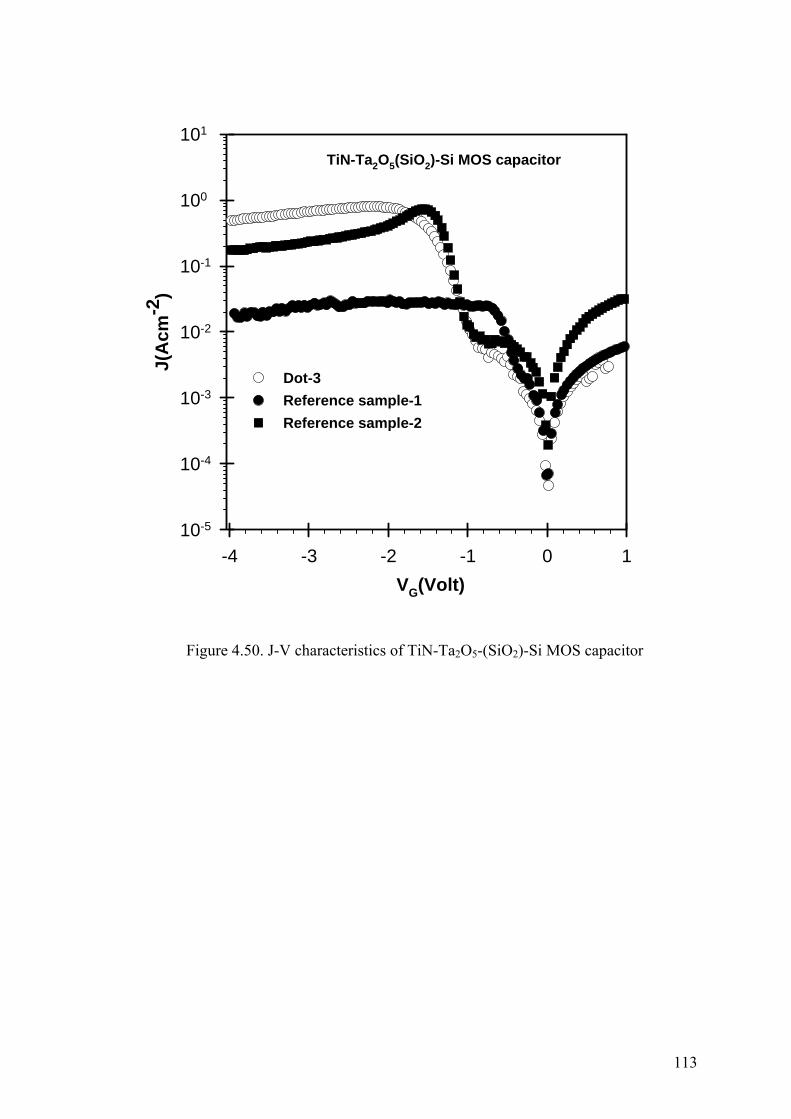
113
Figure 4.50. J-V characteristics of TiN-Ta2O5-(SiO2)-Si MOS capacitor
VG(Volt)-4 -3 -2 -1 0 1
J(A
cm-2
)
10-5
10-4
10-3
10-2
10-1
100
101
TiN-Ta2O5(SiO2)-Si MOS capacitor
Reference sample-1Reference sample-2
Dot-3
114
normalized to the oxide capacitance, surface potential ψs versus gate voltage VG curves
were generated similarly carried out for previous samples (data not shown). Finally, Dit
levels of TiN metal gate samples were calculated as a function of energy and shown in
Figure 4.51. Dit levels are slightly lower than reference sample-2 with Al metal gate.
However, there is a large variation Dit between 1x10¹¹ (eVcm2)-1 and 8x10¹¹ (eVcm2)-1.
It can be inferred that interface of Ta2O5 and silicon substrate is irregularly modified to
give slightly lower Dit values than that of Al metal gate sample. The important data
obtained from high frequency C-V measurement for TiN-Ta2O5(SiO2)-Si MOS
capacitors is summarized in Table 4.9.
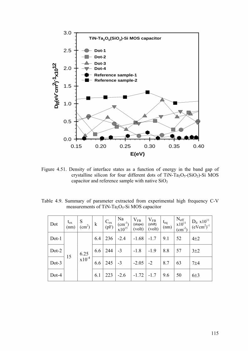
115
Figure 4.51. Density of interface states as a function of energy in the band gap of crystalline silicon for four different dots of TiN-Ta2O5-(SiO2)-Si MOS capacitor and reference sample with native SiO2
Table 4.9. Summary of parameter extracted from experimental high frequency C-V
measurements of TiN-Ta2O5-Si MOS capacitor
Dot tox (nm)
S (cm2) k Cox
(pF)
Na (cm-3) x1015
VFB (slope) (volt)
VFB (shift) (volt)
teq (nm)
Neff x1011 (cm-2)
Dit x1011
(eVcm2)-1
Dot-1 6.4 236 -2.4 -1.68 -1.7 9.1 52 4±2
Dot-2 6.6 244 -3 -1.8 -1.9 8.8 57 3±2
Dot-3 6.6 245 -3 -2.05 -2 8.7 63 7±4
Dot-4
15 6.25 x10⁻⁴
6.1 223 -2.6 -1.72 -1.7 9.6 50 6±3
E(eV)0.15 0.20 0.25 0.30 0.35 0.40
Dit(
eV- c
m2 )
-1x1
012
0.0
0.5
1.0
1.5
2.0
2.5
3.0
Dot-3Dot-4
Dot-1Dot-2
Reference sample-1
TiN-Ta2O5(SiO2)-Si MOS capacitor
Reference sample-2

116
4.5.3 Results of W Metal Gate MOS Capacitor
An alternative gate material is selected as tungsten. It is a steel-gray to tin-white
metal with the highest melting of all metals. It has the highest tensile strength and
excellent corrosion resistance. It shows no inter diffusion with the surrounding materials
and smooth interface with dielectrics. Its work function is 4.5 eV. The fifth group of
samples used in this thesis was prepared using W metal gate. In this group of samples,
RTN process of silicon surface at 700 oC and 850 oC in N2O was applied. Then the Ta
metal films were deposited by RF sputtering method. Dry oxidation of Ta film in O2 at
873 oC was carried out to form high-k Ta2O5 oxide layer. Finally, W metal gate
electrodes were deposited on the oxide using RF sputtering method.
High frequency C-V measurements of several dots from the same substrate were
shown in Figure 4.52a for nitrided sample at 700 oC and in Figure 4.52b for nitrided
sample at 850 oC. The oxide capacitance for both samples is around 300±15 pF, it
shows slight changes among different dots. Dielectric constant calculated from these
oxide charges is 12±0.5 and the equivalent oxide thickness for all dots in both groups of
samples is 7±0.2 nm, giving consistent value among different dots. It can be understood
that nitridation in N2O at 700 oC and 850 oC give almost identical quality oxide layer.
High frequency C-V curves of the samples are used to generate 1/C2 versus gate
voltage VG in order to obtain doping concentration NA and flat band voltage shifts due
to non ideal effects. In Figure 4.53, 1/C2 vs VG plots of W metal gate MOS capacitors
are presented. The value of NA is found to be 2.5x1015 cm-3 for 700 oC samples and
5x1015 cm-3 for 850 oC samples. Both groups of samples show substantial flat band VFB
voltage shifts around -2 V.
The effect of mobile trap charges were characterized by measuring hysteresis
behavior of high frequency C-V curves from accumulation to inversion and back to
accumulation. Examples of hysteresis measurement of one of the Dot from each group
of samples are presented in Figure 4.54a and Figure 4.54b, for 700 oC and 850 oC
samples, respectively. It is important to note that ΔVFB voltage shift in hysteresis curve
is almost insignificant to notice. It is below 30mV and in the acceptable limit of
electronic fabrication of MOS devices. Such low mobile trap charges were measured in
MOS capacitors with thermally grown Ta2O5 oxide layers. These samples are the
reference sample-1 with Al metal gate and the group for sample with TiN metal gate. It

117
Figure 4.52. High frequency capacitance versus gate voltage curves of W-Ta2O5-
(SiOxNy)-Si MOS capacitors for nitridation temperatures at a) 700ºC, b) 850ºC in N2O gas environment
VG(Volt)
-6 -5 -4 -3 -2 -1 0 1
C(p
F)
0
50
100
150
200
250
300
350W metal gateNitrided at 850 oC in N2O
Dot-1
Dot-3Dot-2
Dot-4
b)
-5 -4 -3 -2 -1 0 1
C(p
F)
0
50
100
150
200
250
300
350W m eta l gate N itrided at 700 oC in N 2O
D ot-1
D ot-3D ot-2
D ot-4
a )
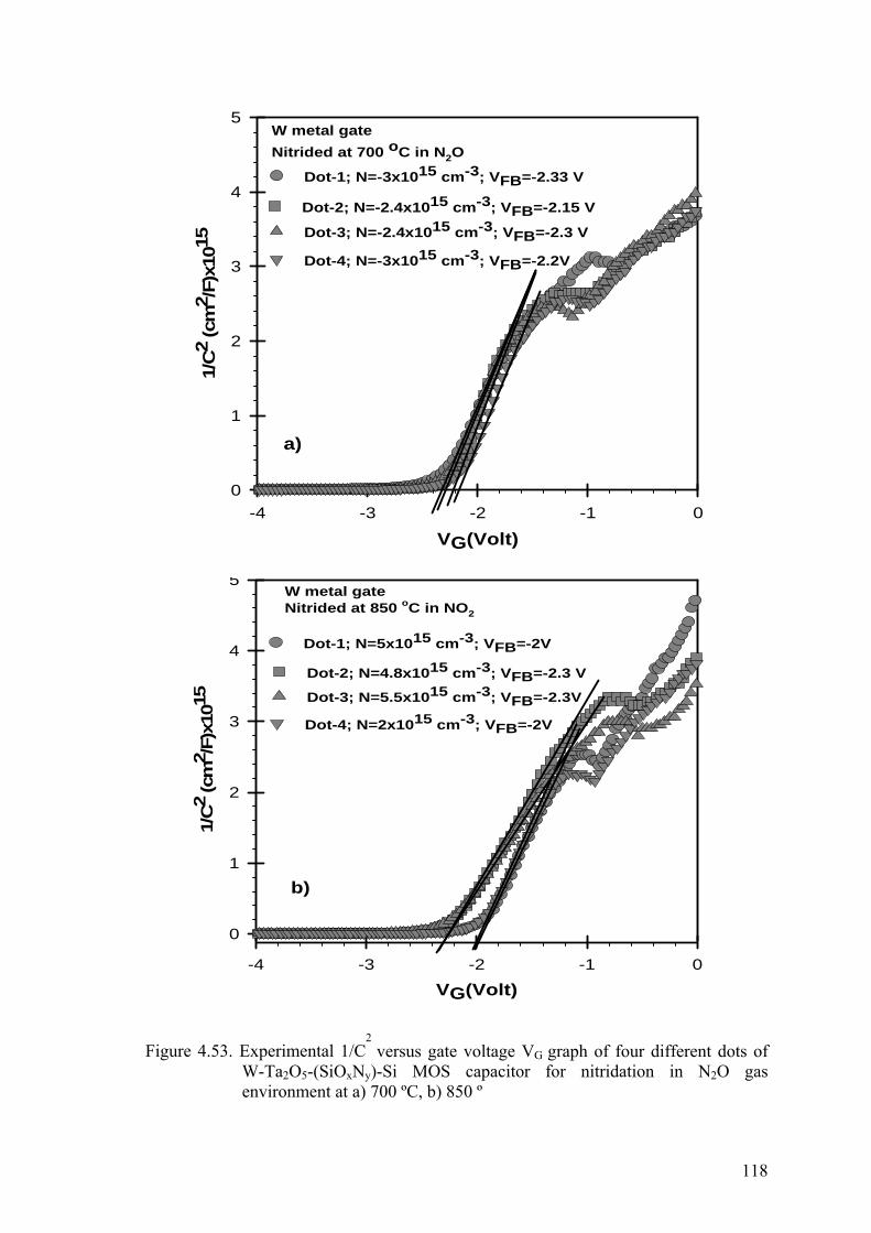
118
Figure 4.53. Experimental 1/C2
versus gate voltage VG graph of four different dots of
W-Ta2O5-(SiOxNy)-Si MOS capacitor for nitridation in N2O gas environment at a) 700 ºC, b) 850 º
VG(Volt)-4 -3 -2 -1 0
1/C
2 (c
m2 /
F)x1
015
0
1
2
3
4
5W metal gateNitrided at 850 oC in NO2
Dot-3; N=5.5x1015 cm-3; VFB=-2.3V
Dot-4; N=2x1015 cm-3; VFB=-2V
Dot-1; N=5x1015 cm-3; VFB=-2V
Dot-2; N=4.8x1015 cm-3; VFB=-2.3 V
b)
VG(Volt)-4 -3 -2 -1 0
1/C
2 (c
m2 /
F)x1
015
0
1
2
3
4
5W metal gateNitrided at 700 oC in N2O
Dot-3; N=-2.4x1015 cm-3; VFB=-2.3 V
Dot-4; N=-3x1015 cm-3; VFB=-2.2V
Dot-1; N=-3x1015 cm-3; VFB=-2.33 V
Dot-2; N=-2.4x1015 cm-3; VFB=-2.15 V
a)

119
Figure 4.54. Forward and reverse C-V curve of W-Ta2O5-(SiOxNy)-Si MOS capacitor
with nitrided Si surface in N2O at a) 700ºC, b) 850ºC
VG(Volt)-7 -6 -5 -4 -3 -2 -1 0 1 2 3
C (p
F)
0
50
100
150
200
250
300
From acc. to inv.
From inv. to acc.
W metal gateNitrided at 700 oC in N2O a)
VG(Volt)-6 -5 -4 -3 -2 -1 0 1 2 3
C (p
F)
0
50
100
150
200
250
300
From acc. to inv.
From inv. to acc.
W metal gateNitrided at 850 oC in N2O b)

120
can be concluded that thermal oxidation of Ta metal films contain almost insignificant
mobile trap charges in contrast to those deposited by RF sputtering process.
Leakage current measurement of W metal gate samples are shown in Figure
4.55a and Figure 4.55b for 700 oC and 850 oC samples, respectively. In inversion
region, substantially lower leakage current than those of reference sample-1 and
reference sample-2 were measured. However, in depletion region at gate voltage of VFB,
leakage currents are exceeding those measured in reference sample 1, but the sample
obtained at 700 oC nitridation is still gives better leakage current at that region than the
reference sample-2.
Theoretical C-V curves of W metal gate samples were also calculated using the
experimental inputs of dielectric constant, oxide thickness, doping concentration of
MOS capacitors. An example of ideal and experimental C-V curves normalized to oxide
capacitance for both group of samples are presented in Figure 4.56a and Figure 4.56b
for 700 oC and 850 oC nitrided samples, respectively. It is clearly seen from Figure 4.56
that there exist a significant flat band voltage shift for W metal gate samples as well.
The values of VFB for different dots are very close to 2.2±0.2 volt similar to those
measured in reference sample-2 with Al metal gate and the same thermally grown
Ta2O5 oxide layer. However, VFB values showed large variations even on dots taken
from the same substrate for MOS capacitor with RF sputtered Ta2O5 oxides and also
with TiN metal gate with thermal Ta2O5 oxide layer. It is interesting that TiN metal gate
has effect on both effective dielectric constant and calculated from oxide capacitance as
well as the density of effective oxide charge. The Neff values of W metal gate MOS
capacitors are summarized in Table 4.10 and Table 4.11 for 700 oC and 850 oC nitrided
samples, respectively. It is almost uniform around 60±12x1011 cm-2 among different
dots taken from the same substrate. It can be concluded that distribution of the effective
oxide charge is more homogeneously distributed in W metal gate MOS capacitors.
The density of interface trap states of W metal gate samples were obtained from
Terman’s method in a similar way carried out for other groups of samples. Dit levels of
MOS capacitors with prior nitridation process in N2O at 700 oC and 800 oC are shown
in Figure 4.7a and Figure 4.57b, respectively. Dit level for 700 oC nitrided sample is
around 3±2x10¹¹ (eVcm2)-1. These values are almost in the similar range of Dit levels
measured for Al metal gates samples prepared with the same nitridation process in N2O
at 700 oC as presented in Figure 4.21. However, Dit levels for nitrided samples at 850 oC
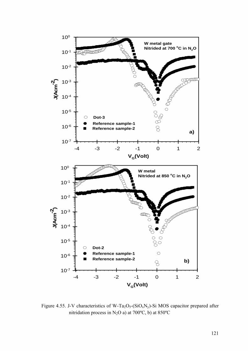
121
Figure 4.55. J-V characteristics of W-Ta2O5-(SiOxNy)-Si MOS capacitor prepared after
nitridation process in N2O a) at 700ºC, b) at 850ºC
VG(Volt)-4 -3 -2 -1 0 1 2
J(A
cm-2
)
10-7
10-6
10-5
10-4
10-3
10-2
10-1
100W metalNitrided at 850 oC in N2O
Reference sample-1Reference sample-2 b)
Dot-2
VG(Volt)-4 -3 -2 -1 0 1 2
J(A
cm-2
)
10-7
10-6
10-5
10-4
10-3
10-2
10-1
100
W metal gateNitrided at 700 oC in N2O
Reference sample-1Reference sample-2
a)
Dot-3

122
Figure 4.56. Normalized experimental and theoretical capacitance versus gate voltage
and conductance versus gate voltage of W-Ta2O5-(SiOxNy)-Si MOS capacitor prepared after nitridation process in N2O at a) 700ºC, b) 850ºC
VG(Volt)
-6 -5 -4 -3 -2 -1 0 1
C/C
ox
0.0
0.2
0.4
0.6
0.8
1.0
G(m
icro
S)
0
50
100
150
200
250
300
Experimental
Theoretical
VFB
Conductance
~VFB
Dot-3 (Nitrided at 700 oC)
a)
VG(Volt)
-6 -5 -4 -3 -2 -1 0 1
C/C
ox
0.0
0.2
0.4
0.6
0.8
1.0
G(m
icro
S)
0
50
100
150
200
250
300
350
400
Experimental
Theoretical
VFB
Conductance
~VFB
Dot-2 (Nitrided at 850 oC)
b)

123
Figure 4.57. Density of interface states as a function of energy in the band gap of crystalline silicon for reference samples and four different dots of W-Ta2O5-(SiOxNy)-Si MOS capacitor for nitridation in N2O gas environment at a) 700°C, b) 850°C
E(eV)0.15 0.20 0.25 0.30 0.35 0.40
Dit(
eV- c
m2 )
-1x1
012
0.0
0.5
1.0
1.5
2.0
2.5
3.0
Dot-3Dot-4
Dot-1Dot-2
Reference sample-1
W metal gateNitridation at 700 oC in N2O a)
Reference sample-2
E(eV)0.15 0.20 0.25 0.30 0.35 0.40
Dit(
eV- c
m2 )
-1x1
012
0.0
0.5
1.0
1.5
2.0
2.5
3.0
Dot-3Dot-4
Dot-1Dot-2
Reference sample-1
W metal gateNitridation at 850 oC in NO2
Reference sample-2
b)

124
show larger scattering and is around 5±4x10¹¹ (eVcm2)-1. Dit levels for sample prepared
with the same nitridation process at the same temperature with Al metal gate was
measured to be 3±2x10¹¹ (eVcm2)-1 as shown in Figure 4.28. Dit levels of W metal gate
samples for different dots were also summarized in Table 4.10 and Table 4.11 for 700 oC and 850 oC nitrided samples, respectively.
Table 4.10. Summary of parameter extracted from experimental high frequency C-V measurements of W-Ta2O5-(SiOxNy)-Si-MOS capacitor prepared after nitridation process at 700ºC in N2O gas ambient
Table 4.11. Summary of parameter extracted from experimental high frequency C-V measurements of W-Ta2O5-(SiOxNy)-Si-MOS capacitor prepared after nitridation process at 850ºC in N2O gas ambient
Dot tox (nm)
S (cm2) k Cox
(pF)
Na (cm-3) x1015
VFB (slope) (volt)
VFB (shift) (volt)
teq (nm)
Neff x1011 (cm-2)
Dit x1011
(eVcm2)-1
Dot-1 11.8 298 -3 -2.33 -2.45 7.2 68 2±2
Dot-2 12.4 318 -2.4 -2.15 -2.2 6.9 70 4±2
Dot-3 12.09 302 -2.4 -2.3 -2.4 7.1 52 3±1
Dot-4
22 6.25 x10⁻⁴
11.6 290 -3 -2.2 -2.3 7.4 66 4±2
Dot tox (nm)
S (cm2) k Cox
(pF)
Na (cm-3) x1015
VFB (slope) (volt)
VFB (shift) (volt)
teq (nm)
Neff x1011 (cm-2)
Dit x1011
(eVcm2)-1
Dot-1 11.8 296 -5 -2 -2.1 7.2 47 5±1
Dot-2 12.3 308 -4.8 -2.3 -2.4 6.9 54 5±4
Dot-3 12.4 311 -5.5 -2.3 -2.4 6.9 75 4±3
Dot-4
22 6.25 x10⁻⁴
12.5 315 -4.4 -2 -2.1 6.8 66 6±2
125
4.5.4 Conclusions
In the last part of thesis, the second objective, the effect of different metal gates
on the characteristics of MOS capacitors, were investigated using three different gate
metal, Al, TiN and W deposited on similar Ta2O5 oxide layers. Reference Sample 1 and
Reference Sample 2 were also used for the comparison of the improvements in oxide
and interface properties of MOS capacitors with different metal gates.
MOS capacitors in the form of Al- Ta2O5-(SiO2)-Si and TiN-Ta2O5-(SiO2)-Si
have different metal gates but the same Ta2O5 formation process on silicon surface.
There was no prior nitridation of silicon surface was carried out in these two group
MOS capacitors. Only the effect of Al and TiN gate metals on the top interface of gate
metal-gate oxide on the oxide and silicon-Ta2O5 interface quality were investigated
from the high frequency C-V results. It was found that both group of samples showed
very low level of moving trap charges as detected from the hysteresis C-V curves, with
negligible ΔVFB voltage shifts. It can be concluded that gate metal has no effect on the
density of moving trap charges, which is mainly determined by the method of Ta2O5
oxide formation process. In both group thermal oxidation of Ta films in dry O2 was
used to form Ta2O5 oxide layers. However, there are major differences in dielectric
constant, effective oxide charges and the density of interface traps between Al metal
gate and TiN metal gates samples. Dielectric constant of 11.2 was observed for Al metal
gate samples but it decreases to 6.2 for TiN MOS capacitors. The density of effective
oxide charges is 3.0x1012 cm-2 for Al metal gate samples. It increases to 5.5±1 x 10¹²
cm-2 for MOS capacitor with TiN gate metal. However, the density of interface traps
improves significantly from 1.1±1 x10¹² (eVcm2)-1 for Al metal gate to the level of
4±2x10¹¹ (eVcm2)-1 for TiN metal gate MOS capacitors.
The effect of W gate metal on the characteristics of MOS capacitors were
compared with the samples Al metal gate. Both group of samples had the same prior
nitridation process of silicon surface in N2O gas prior Ta2O5 oxide formation. In
addition, deposition method of Ta2O5 was also identical. It was found that large
hysteresis effect was observed in Al metal gate MOS capacitors. However, it is almost
negligible for W metal gate samples. Dielectric constant for the same nitridation process
is slightly lower for Al metal gate MOS capacitors indicating an interfacial layer formed
at top interface by Al gate metal. For both nitridation temperatures, W metal gate
126
samples give almost identical dielectric constant with values around 12, which is
significantly higher that those of Al metal gates. As the oxide and interface quality was
compared, both Al and W MOS capacitors give similar values of high density of
effective oxide charges and interface trap states.
127
CHAPTER 5
DISCUSSIONS AND CONCLUSIONS
High-k dielectric materials are important field of investigation for scaling down
the electronic devices in today’s microelectronic technology to replace native oxide
SiO2 used as gate oxide in DRAM applications. Using high-k dielectric layers for
replacement of SiO2 allow us to use physically thicker oxide layer to obtain the same
oxide capacitance of conventional SiO2 layer in devices with gate oxide below 50nm
scale. This will provide low leakage currents through the gate oxide. In order to achieve
such replacement of SiO2, a new dielectric material must have higher dielectric constant
than SiO2, thermodynamically stable with silicon, low leakage currents and low level of
effective oxide charges. Most of high-k dielectric materials have instability problem
with silicon and resulting in rough interface between silicon and gate oxide and high
level of interface trap density. In addition, high density of effective oxide charges and
moving trap charges present in high-k oxide layers cause deterioration in device
performance. Furthermore, the effective oxide thickness obtained with high-k oxide
layer, EOT, is also determined from the top metal gate electrode used for the
replacement of doped poly-silicon gate electrode. Since most of metal gate materials
interact with underlying oxide layer and form very thin metal oxide at top interface in
series with gate oxide with lower dielectric constant, which finally reduces the effective
dielectric constant of high-k oxide layer. Therefore, it is imperative to investigate the
effects of metal gates together with high-k oxide layers to replace native oxide SiO2. In
this thesis, tantalum pentoxide dielectric materials, Ta2O5, deposited on silicon substrate
using different methods were investigated. In order to provide better interface with
silicon substrate and a barrier between silicon and thermodynamically unstable high-k
oxide layer, a prior nitridation of silicon surface in N2O and NH3 gas using rapid
thermal nitridation process has been used before Ta2O5 oxide formation. The effects of
prior nitridation process on interface quality of silicon- Ta2O5 structure were compared
with unnitrided samples with the same Ta2O5 oxide layer and the same metal gate
electrodes. In addition, three different metal gates, Al, TiN and W, were used with the
same quality Ta2O5 oxide layers underneath. Their effects on oxide and interface
properties of MOS capacitor with high-k oxide layers were investigated. In order to
128
compare the improvements in device characteristics by using different nitridation
process and different metal gates, a reference sample, Reference Sample 1, with native
oxide SiO2 and a second reference sample, Reference Sample 2, with unnitrided silicon
surface and Ta2O5 gate oxide were used. Both reference samples had Al metal gate
electrodes. Characterization different MOS capacitors was performed using high
frequency C-V method and effective dielectric constant, density of mobile trap charges,
effective oxide charges and interface traps were obtained from the analysis of
experimental and ideal C-V curves.
The characteristics of Reference Sample 1 were found that it had insignificant
hysteresis shift in high frequency C-V curve with less than 30 mV ΔVFB voltage shift,
low density of effective oxide charges and very smooth Si-SiO2 interface with Dit level
of 1-2 x1011 cm-2 eV-1. The same level of Dit were obtained from both Terman’s method
and the simultaneous C-V software. These values are very close to that reported for the
best quality Si-SiO2 interface (Manchanda et al. 1998). In Reference Sample 2, native
oxide SiO2 is replaced by thermally grown Ta2O5 high-k oxide layer with the same
oxide thickness of 20nm. Effective dielectric constant increased to 12 as expected and
hysteresis shift in high frequency C-V curve is still less than 30 mV ΔVFB, required for
good quality oxide layer. However, leakage currents are substantially higher, density of
effective oxide charges and that of interface traps are one order of magnitude higher that
that of reference Sample 1. This indicated that Ta2O5 creates very rough interface with
silicon substrate and contains high density of oxide charges even though there is an
improvement in effective dielectric constant. Such high value of oxide charges for
Ta2O5 oxide layers are in good agreement with the reported results in the literature
(Wilk, Wallace and Anthony 2001, Atanassova et al. 2002a).
In order to improve the stability of Ta2O5 oxide layer with silicon substrate, a
novel approach called rapid thermal nitridation (RTN) process (Sun and Chen 1994) has
been applied before high-k oxide formation. In this thesis, a prior nitridation process of
p-type silicon surface in N2O and NH3 gasses at temperature between 700 oC and 850 oC was carried out before deposition of Ta2O5 oxide layers. All nitrided samples had the
structure of Al-Ta2O5-(SiOxNy)-p-Si. Nitridation in N2O were carried out at 700 oC, 800 oC, and 850 oC and nitridation in NH3 was carried out at 700 oC and 800 oC. After that
growth of Ta2O5 was carried out by using RF magnetron sputtering of Ta target in Ar
and O2 gas ambients. Finally, Al metal gates were evaporated using shadow mask with
well defined gate areas.

129
The results of nitridation in N2O for three different temperatures indicate that
there is significant improvement in the interface quality between silicon and Ta2O5
interface from that of unnitrided Reference Sample 2. Here, nitridation process in N2O
creates very thin (1-2 nm) SiOxNy interfacial layer to protect silicon substrate from
instable Ta2O5 oxide and thus low level of interface trap density. Dit levels obtained
from several dots on the same substrate are very close to the value of (2-3) ±1x1011 cm-2
eV-1 for three different nitridation temperatures. These values of Dit are very close to
that measured for Reference Sample 1 with smooth gate oxide SiO2. The obtained
results for the Dit levels are in good agreement with the recent results given in the
literature (Novkovski et al. 2005). Therefore, RTN is a promising process to integrate
into silicon processing technology. However, there are major issues related to other
non-ideal effects present in the gate oxide. First, effective dielectric constant k
decreased to 6 for nitrided samples at 700 C and 800 C from the value of 12 of
unnitrided Reference Sample 2. Then it increases to 10.3 for nitridation at 850 C. The
increase in dielectric constant results in a decrease in EOT for samples at 850ºC. This
can be attributed to highly stable SiOxNy formation on silicon surface, which prevents
the interaction with Ta2O5 oxide layer. It was reported by Park et al. that formation of
AlNx as an interfacial layer between gate metal and gate oxide results in an increase in
equivalent oxide thickness thus a decrease in oxide capacitance values (Park et al.
2003). On the other hand, according to Atanassova et al., Al react with Ta2O5 to form
Al2O3 or Al suboxides. In our case, nitrogen might diffuse inside the oxide and to top
interface of Al-Ta2O5 and there might results in a generation of AlNx or Al2O3
interfacial layers for nitrided samples at 700 oC and 800 oC.
The second effect is that all nitrided samples in N2O gas show large hysteresis
C-V curves with ΔVFB flat band voltage shifts between 30mV and 800 mV even on
different dots taken from the same substrate. This indicates that there is a variation in
the density of moving trap charges and most samples show large density of moving trap
charges. The third effect is that leakage currents in depletion region around flat band
voltage are much higher that that measured in reference Sample 1. The fourth effect is
that flat-band voltage shift of experimental C-V curve from the ideal one is higher than
Reference Sample 1 and it even shows variations among the dots taken from the same
substrate. Consistent values of VFB were obtained from both 1/C2 vs VG and from the
shift of ideal and experimental C-V curves as well as that obtained from the peak
position of conductance versus gate voltage for each dot. The values of Neff calculated
130
from the VFB change between 2x1012 cm-2 and 5x1012 cm-2, which are an order of
magnitude higher than Reference Sample 1. The non-uniformity in the flat band
voltage, thus in Neff, can be attributed to non-uniform nitrogen penetration inside the
oxide, since excessive nitrogen inside the oxide results in oxide charge defect, which in
turn results in device instability as reported in the literature (Wristers et al. 1996).
Moreover, another confirmation of non uniform nitrogen penetration towards the oxide
layer is that the peak value of conductance, one of the most important parameter gate
oxide, increased by several times above the level of Reference Sample 2 without any
nitrided layer and reached to the values between 330 μS and 450μS. All nitrided
samples in N2O at three different temperatures exhibit the similar characteristics in
terms of effective oxide charges and hysteresis effect. But preferred nitridation
temperature could be 850 oC in N2O since the highest effective dielectric constant of
10.3 and the lowest equivalent oxide thickness were obtained at this nitridation
temperature.
In order to improve interface of silicon and Ta2O5, second nitridation process of
silicon surface was performed using NH3 gas at 700 oC and 800 oC. Nitrogen rich SixNy
interfacial layer of 1-2nm has been formed on silicon. The samples were in the form of
Al-Ta2O5-(SiOxNy)-Si. The highest dielectric constant of 12 was obtained for the
samples nitrided at 700 oC and it decreases as nitridation temperature decreases. A main
difference in C-V curve from those nitrided in N2O is that C-V curve in accumulation
region show two steps which is due to trapping on slow states as reported in literature
(Novkovski et al. 2005). All samples nitrided at 700 oC and 800 oC show large
hysteresis shift in C-V curves, the same as observed in those nitrided in N2O gas.
Therefore, it can be inferred that large hysteresis behavior could be due to the
nitridation process or RF sputtering techniques of the oxide layer since both Reference
Sample-1 and Reference Sample-2 were prepared with thermally grown Ta2O5 oxide
layer and both exhibited insignificant hysteresis shifts.
Furthermore, high values of flat band voltage shifts VFB and even large variation
in VFB were obtained among the dots taken from the same substrate, the same as
observed in N2O nitrided samples. Similar levels of effective oxide charges were also
calculated in NH3 nitrided samples as well. This could be due to both nitrogen and
hydrogen diffusion towards oxide layer since this can cause high level of oxide charges
and increases conductance through the gate oxide. In fact, the peak value of
conductance curve for NH3 samples are slightly higher than those measured in N2O

131
nitrided samples as presented in conductance vs gate voltage figures. Finally, the
density of interface traps for samples nitrided in NH3 was lower than Reference sample
2. However, the Dit level for 700 oC nitrided sample shows a variation around
(4±3)x1011 (eVcm2)-1 and increases slightly to (6±3)x1011 (eVcm2)-1 for 800 oC nitrided
samples. These values are slightly higher than those of N2O nitrided samples. The
important note is that the interface between silicon and Ta2O5 oxide layer is not
smoother than those obtained for N2O nitrided samples. The interface is deteriorated in
NH3 nitridation. The reason for this could be due to the fact that N2O nitridation
provides oxygen rich SiOxNy which causes a decrease in the Dit levels at silicon-Ta2O5
interface. However, the presence of NH3 gives raise to formation of nitrogen rich
SiOxNy, which increase the roughness of the interface.
In conclusion, these results of prior nitridation process indicate that nitridation
process provide substantial improvement in interface properties of silicon-Ta2O5 high-k
oxide. However, it does not improve the oxide charge properties such as moving trap
charges and effective oxide charges and even the leakage current density. Moreover,
with the uncontrolled nitridation process, the oxide charge properties can be worsened.
Therefore, further investigation is needed to understand the nature of these oxide
charges present in MOS devices with high dielectric constant materials.
The second objective of this thesis was to investigate the effects of different
metal gates on overall performance of the MOS devices with high-k oxide layers. For
this purpose, samples with three different metal gates were studied in detail. These are
Al, TiN and W metal gates. The high-k Ta2O5 oxide layers underneath were maintained
to be the same quality in order to see the effect of different metal gate on measured
characteristics of MOS devices. The first group of samples has the form of Al-Ta2O5-
(SiO2)-Si ( Reference Sample 2), the second group has the form of Al- Ta2O5-(SiOxNy)-
Si, the third group of samples has the form of TiN-Ta2O5-(SiO2)-Si and fourth group of
samples has the form of W- Ta2O5-(SiOxNy)-Si structure. Here, the effects of Al and
TiN metal gates were compared using MOS capacitors with the same thermally grown
Ta2O5 oxide layer on silicon substrate. It was found that both group of samples have
very low level of moving trap charges with insignificant ΔVFB voltage shifts below
30mV in hysteresis C-V, high level of effective oxide charges and leakage currents.
Major difference is that effective dielectric constant is 12 for Al metal gate sample and
it is around 6 for TiN metal gate MOS capacitor. Both had the same gate area but Al
metal gate sample has 20 nm and TiN sample had 15 nm oxide thickness. The result of
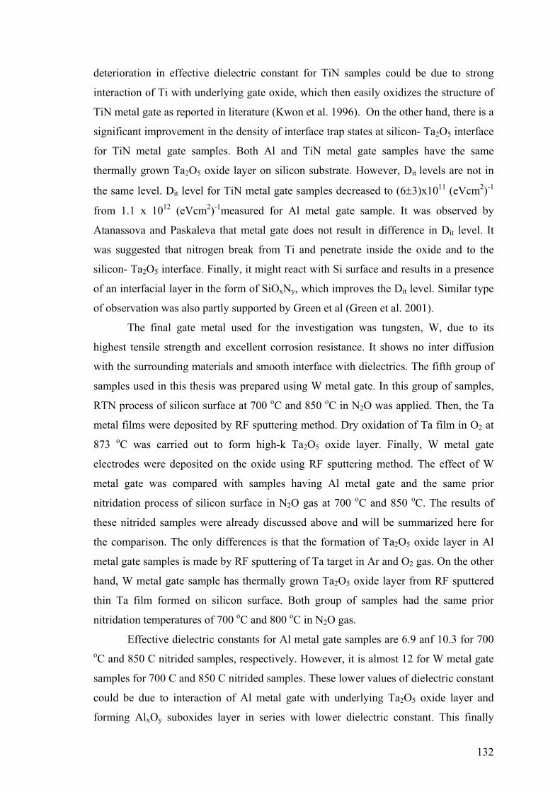
132
deterioration in effective dielectric constant for TiN samples could be due to strong
interaction of Ti with underlying gate oxide, which then easily oxidizes the structure of
TiN metal gate as reported in literature (Kwon et al. 1996). On the other hand, there is a
significant improvement in the density of interface trap states at silicon- Ta2O5 interface
for TiN metal gate samples. Both Al and TiN metal gate samples have the same
thermally grown Ta2O5 oxide layer on silicon substrate. However, Dit levels are not in
the same level. Dit level for TiN metal gate samples decreased to (6±3)x1011 (eVcm2)-1
from 1.1 x 10¹² (eVcm2)-1measured for Al metal gate sample. It was observed by
Atanassova and Paskaleva that metal gate does not result in difference in Dit level. It
was suggested that nitrogen break from Ti and penetrate inside the oxide and to the
silicon- Ta2O5 interface. Finally, it might react with Si surface and results in a presence
of an interfacial layer in the form of SiOxNy, which improves the Dit level. Similar type
of observation was also partly supported by Green et al (Green et al. 2001).
The final gate metal used for the investigation was tungsten, W, due to its
highest tensile strength and excellent corrosion resistance. It shows no inter diffusion
with the surrounding materials and smooth interface with dielectrics. The fifth group of
samples used in this thesis was prepared using W metal gate. In this group of samples,
RTN process of silicon surface at 700 oC and 850 oC in N2O was applied. Then, the Ta
metal films were deposited by RF sputtering method. Dry oxidation of Ta film in O2 at
873 oC was carried out to form high-k Ta2O5 oxide layer. Finally, W metal gate
electrodes were deposited on the oxide using RF sputtering method. The effect of W
metal gate was compared with samples having Al metal gate and the same prior
nitridation process of silicon surface in N2O gas at 700 oC and 850 oC. The results of
these nitrided samples were already discussed above and will be summarized here for
the comparison. The only differences is that the formation of Ta2O5 oxide layer in Al
metal gate samples is made by RF sputtering of Ta target in Ar and O2 gas. On the other
hand, W metal gate sample has thermally grown Ta2O5 oxide layer from RF sputtered
thin Ta film formed on silicon surface. Both group of samples had the same prior
nitridation temperatures of 700 oC and 800 oC in N2O gas.
Effective dielectric constants for Al metal gate samples are 6.9 anf 10.3 for 700 oC and 850 C nitrided samples, respectively. However, it is almost 12 for W metal gate
samples for 700 C and 850 C nitrided samples. These lower values of dielectric constant
could be due to interaction of Al metal gate with underlying Ta2O5 oxide layer and
forming AlxOy suboxides layer in series with lower dielectric constant. This finally
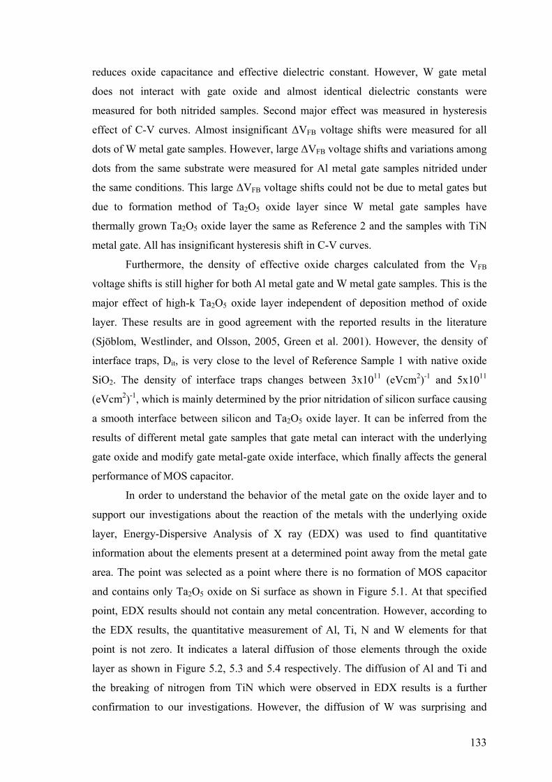
133
reduces oxide capacitance and effective dielectric constant. However, W gate metal
does not interact with gate oxide and almost identical dielectric constants were
measured for both nitrided samples. Second major effect was measured in hysteresis
effect of C-V curves. Almost insignificant ΔVFB voltage shifts were measured for all
dots of W metal gate samples. However, large ΔVFB voltage shifts and variations among
dots from the same substrate were measured for Al metal gate samples nitrided under
the same conditions. This large ΔVFB voltage shifts could not be due to metal gates but
due to formation method of Ta2O5 oxide layer since W metal gate samples have
thermally grown Ta2O5 oxide layer the same as Reference 2 and the samples with TiN
metal gate. All has insignificant hysteresis shift in C-V curves.
Furthermore, the density of effective oxide charges calculated from the VFB
voltage shifts is still higher for both Al metal gate and W metal gate samples. This is the
major effect of high-k Ta2O5 oxide layer independent of deposition method of oxide
layer. These results are in good agreement with the reported results in the literature
(Sjöblom, Westlinder, and Olsson, 2005, Green et al. 2001). However, the density of
interface traps, Dit, is very close to the level of Reference Sample 1 with native oxide
SiO2. The density of interface traps changes between 3x10¹¹ (eVcm2)-1 and 5x10¹¹
(eVcm2)-1, which is mainly determined by the prior nitridation of silicon surface causing
a smooth interface between silicon and Ta2O5 oxide layer. It can be inferred from the
results of different metal gate samples that gate metal can interact with the underlying
gate oxide and modify gate metal-gate oxide interface, which finally affects the general
performance of MOS capacitor.
In order to understand the behavior of the metal gate on the oxide layer and to
support our investigations about the reaction of the metals with the underlying oxide
layer, Energy-Dispersive Analysis of X ray (EDX) was used to find quantitative
information about the elements present at a determined point away from the metal gate
area. The point was selected as a point where there is no formation of MOS capacitor
and contains only Ta2O5 oxide on Si surface as shown in Figure 5.1. At that specified
point, EDX results should not contain any metal concentration. However, according to
the EDX results, the quantitative measurement of Al, Ti, N and W elements for that
point is not zero. It indicates a lateral diffusion of those elements through the oxide
layer as shown in Figure 5.2, 5.3 and 5.4 respectively. The diffusion of Al and Ti and
the breaking of nitrogen from TiN which were observed in EDX results is a further
confirmation to our investigations. However, the diffusion of W was surprising and
134
implies that if more controlled formation method of W is succeeded, even better
electrical characteristics can be obtained for the sample with W metal gates.
Based on these results, it can be concluded that, the use of metal gate on high-k
dielectric material used in DRAMs introduces its own capacitor quality challenges. As
the electrical characteristics of Ta2O5 film with different metal gate analyzed, it was
obtained that, EOT, current density, flat band voltage and dielectric constant were all
highly depended on the gate metal while hysteresis and interface characteristics are
depend on the high-k dielectric materials deposition technique. Therefore, the more
general conclusion is that, the choice of the gate material and deposition technique of
the high-k for DRAMs application is a critical concern for high-k dielectric materials.
More investigations are required to resolve such critical issues present in high-k oxide
layers.
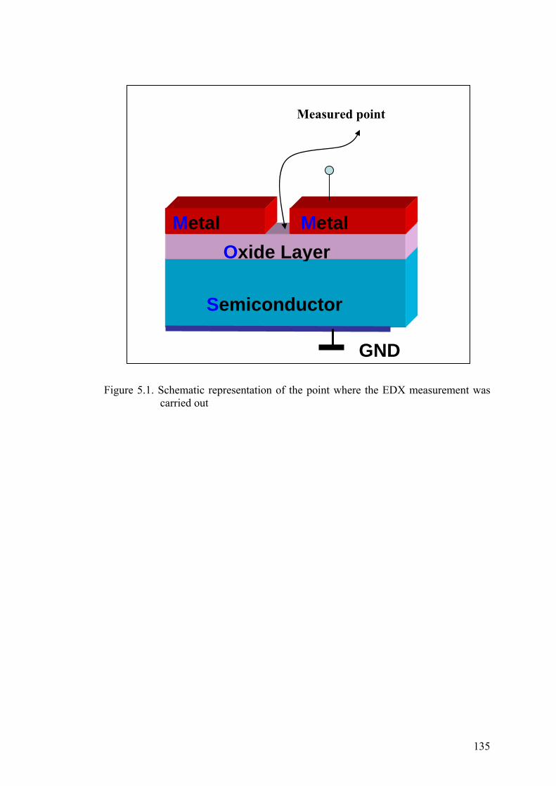
135
Figure 5.1. Schematic representation of the point where the EDX measurement was
carried out
GND
Oxide LayerMetal Metal
Semiconductor
Measured point
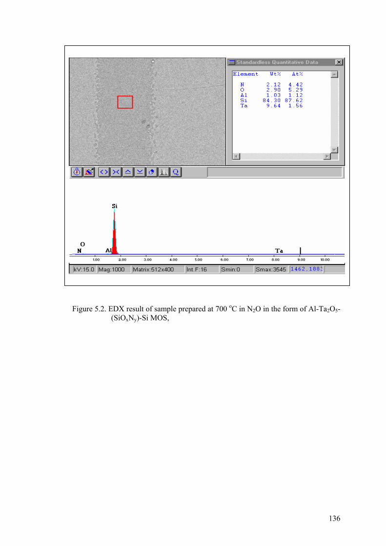
136
Figure 5.2. EDX result of sample prepared at 700 oC in N2O in the form of Al-Ta2O5-(SiOxNy)-Si MOS,

137
Figure 5.3. EDX result of sample prepared in the form of TiN-Ta2O5-(SiO2)-Si,
138
Figure 5.4. EDX result of sample prepared at 700 oC in N2O in the form of W-Ta2O5-(SiOxNy)-Si MOS capacitor

139
5.1 Future work
In this thesis, it was found that a prior nitridation process in N2O and NH3 gas is
a promising method for improving silicon- Ta2O5 interface, especially nitridation at 850 oC in N2O and nitridation in NH3 at 700 oC gives better interface and higher dielectric
constants. However, formation of Ta2O5 using RF magnetron sputtering from Ta target
in Ar and O2 gas causes large hysteresis effect. Instead thermal oxidation of Ta films in
dry oxygen could be oxide formation method since no moving trap charges exists in
those oxide layer It is soft growth process in contrast to the magnetron sputtering of Ta
target. Investigations should focus on improving device processing conditions to
decrease the levels of effective oxide charges and leakage currents to the level of native
oxide SiO2 by keeping the high dielectric constant and better interface properties. In
addition, non-interacting gate metal candidate could be tungsten. The research for the
gate metal and high-k dielectric should be carried out together in order to solve complex
problems together.

140
REFERENCE
Atanassova, E. and Spassov, D. 1998. “Electrical properties of thin Ta2O5 films
obtained by thermal oxidation of Ta on Si”, Microelectronic Reliability. Vol. 38,
pp.827-832.
Atanassova, E. 1999. “Thin RF sputtered and thermal Ta2O5 on Si for high density
DRAM application”, Microelectronics Reliability. Vol. 39, pp. 1185-1217.
Atanassova, E., Kalitzova, M., Zollo, G., Paskaleva, A., Peeva, A., Georgieva, M., and
Vitali, G. 2003. "HRTEM and RHEED study of oxygen annealing induced
ctystallization in Ta2O5 layers", Thin Solid Films. Vol. 426, No.191.
Atanassova, E., Novkovski, N., Paskaleva, A., and Pecovska-Gjorgjevich, M. 2002a.
"Conduction mechanisms in thin rf sputtered Ta2O5 on Si", Solid-State Electron.
Vol. 46, p.1887.
Atanassova, E., Spassov, D., Paskaleva, A., Koprinarova, J. Georgieva, M., 2002b.
“Influence of oxidation temperature on the microstructure and electrical
properties of Ta2O5 on Si”, Microelectronics Journal. Vol. 33, pp. 907-920.
Atanassova, E., Paskaleva, A. 2006. “Challenges of Ta2O5 as High-k Dielectric for
Nanoscale DRAM’s”, Proceeding of 25th International Conference on
Microelectronics (MIEL 2006), Belgrade, Serbia and Montenegro, (14-17 May).
Babeva, Tz., Atanassova, E., and Koprinarova, J. 2005. “Optical characteristic of thin rf
sputtered Ta2O5 layers”, phys. stat. sol. (a) 202, No. 2, pp.330–336.
Berglund, C. N. 1966. “Surface States at Steam-Grown Silicon-Silicon Dioxide
Interfaces”, IEEE Trans. Electron Devices. Vol. ED-13, p. 701.

141
Brown D. M. and Gray, P. V. 1968. “Si-SiO2 Fast Interface State Measurements,” J.
Electrochem. SOC., Vol. 115, p. 760.
Buchanan, D.A., DiMaria, D.J.. Chang, C-A and Taur, Y. 1994. “Defect generation in
3.5 nm silicon dioxide films”, Apply Physics. Letter. Vol.65, No.14, pp.1280-
1282.
Butler Z. Ç. and Hsiang, T. Y. 1988. “Determination of Si-SiO2 Interface Trap Density
by 1/f Noise Measurement”, IEE Trans. Electron Devices. Vol. 35, No.10.
Callegari, A., Cartier, E., Gribelyuk, M., Okorn-Schmidt, H. F. and Zabel, T. 2001.
“Physical and Electrical Characterization of Hafnium Oxide and Hafnium
Silicate Sputtered Films”, Journal of Applied Physics. Vol. 90, No. 12. pp. 6466-
6475.
Campbell, S. A., 2001. “The Science and Engineering of Microelectronic Fabrication”,
2nd. Edition (Oxford University. Press, New York), pp. 68-95.
Campbell, S. A., Gilmer, D.C. Wang, X-C., Hsieh, M-T., Kim, H-S., Gladfelter, W. L.
and Yan, J., 1997, “MOSFET Transistors Fabricated With High Permittivity
TiO2 Dielectrics”, IEEE Trans. Electron Devices. Vol. 44, p.104.
Cao, M., Vande, P., Cox, M., Greene, W. 1998. “Boron Diffusion and Penetration in
Ultra thin Oxide with Poly-Si Gate”, IEEE Electron device letters. Vol. 19, No.
8.
Cartier, E., He, B., Gousev, E., Buchanan, D. A., Okorn-Schmidt, H. F., Copel, M. and
Gribelyuk, M. 2000. “Proceedings of the Material Research Society”, MRS,
San Francisco, Ca,
Casey, Jr., H. C. 1999. “Devices for Integrated Circuits: Silicon and III-V Compound
Semiconductors” John Wiley & Sons, New York.

142
Chakraborty, S., Samanta, S. K., Bhattacharya, S., McCarthy, J., Armstrong, B. M.,
Gamble, H. S., Dalapati, G. K., Das, S., Perova, T. S., Moore, R. A., and Maiti,
C. K. 2004. “Electrical Properties of High-k Ta205 Gate Dielectrics on Strained
Ge-rich Layers”, Proc. 24th International conference on microelectronics [MIEL
2004), VOL 2, Nls, Serbia Montenegro 16-1 9 may, pp. 483-486.
Chau, R., Kavalieros, J., Roberds, B., Schenker, R., Lionberger, D., Barlage, D., Doyle,
B., Arghavani, R., Murthy, A., and Dewey, G. 2000. “30 nm Physical Gate
Length CMOS Transistors with 1.0 ps n-MOS and 1.7 ps p-MOS Gate Delay”,
Tech. Dig. Int. Electron Device Meet., pp.45-48
Chen, K., Nielsen, M., Yang, G. R., Rymaszewski, E. J., and Lu, T-M. 1997. “Study of
amorphous Ta2O5 thin films by DC magnetron reactive sputtering”, Journal of
Electronic Materials.
Dimitrova, T. and Atanassova E. 1998a. “Carrier mobility in inversion layers of Si-thin
Ta2O5 structures”, Microelectronics Reliability. Vol. 38, pp.833-837.
Dimitrova T. and Atanassova, E. 1998b. “Interface and oxide properties of rf sputtered
Ta2O5-Si structures”, Vacuum. Vol.51, No.2, pp.151-152.
Dimitrova, T. and Atanassova, E. 1998c. “Electrical and transport properties of RF
sputtered Ta2O5 on Si”, Solid-State Electronics. Vol.42, No.3, pp.307–315.
Dimitrova, T., Arshak, K., Atanassova, E. 2001. “Crystallization effects in oxygen
annealed Ta O thin films on Si” Thin Solid Films 381, p. 31- 38.
Ezhilvalavan, S., Tseng, Y.T. 1999. “Preparation and Properties of Tantalum Pentoxide
(Ta2O5) Thin Films For Ultra Large Scale Integrated Circuits (ULSIs)
Application- A review”, Journal of Material Science. vol. 10, pp. 9-31.
Fillot, F., Chenevier, B., Maîtrejean, S., Audier, M., Chaudouët, P., Bochu, B.,
Sénateur, J. P., Pisch, A., Mourier, T., Monchoix, H., Guillaumot, B., and

143
Passemard, G. 2003. “Investigation of the Interface Stability in HfO2-Metal
Electrodes”, Elsevier Science B.V. doi:10.1016/S0167-9317(03)00428-3.
Gou, X. and Ma, T. P. 1998. “Tunneling leakage current in oxynitride: dependence on
oxygen /nitrogen content”, IEEE Electron Device Letter. Vol. 19, pp. 207-209.
Green, M. L., Gusev, E. P., Degraeva, R., Garfunkel, E.L. 2001. “Ultrathin (<4 nm)
SiO2 and Si–O–N gate dielectric layers for silicon microelectronics:
Understanding the processing, structure, and physical and electrical limits”
Journal of Applied Physics. Vol. 90, No. 5, pp. 2057-2121.
Gray P. V.and Brown, D. M. 1966. “Density of Si02-Si Interface States,” Applied
Physics Letter. vol. 8, p. 31.
Groner M.D., Elam, J.W., Fabreguette, F.H., George, S.M. 2002. “Electrical
Characterization of thin Al2 O3 Films Grown by Atomic Layer Deposition on
Silicon and Various Metal Substrates”, Thin Solid Films. Vol. 413, p.186–197.
Gusev, E. P., Lu, H.-C., Garfunkel, E. L., Gustafsson, T., Green, M. L. 1999. ”Growth
and Characterization of Ultrathin Nitrided Silicon Oxide Films”, IBM J. RES.
DEVELOP. Vol. 43, No. 3, pp. 265-286
Han, L. K., Yoon, G. W., Kwong, D. L., Mathews, V. K., and Fazan, P. C. 1998.
“Effects of post-deposition annealing on the electrical properties and reliability
of Ultra thin Chemical Vapor Deposited Ta2O5 films”, IEEE Electron Device
Letters. V. 15, No. 8, pp.280-282.
Han, S. 2003. “Fabrication and Device Characterization of Alternative Gate Stacks
Using the Non Self-Aligned Gate Process”, April, 2003.
I. S. Jeon, J. Park, D. Eom, C. S. Hwang, H. J. Kim, C. J. Park, H.Y. Cho, Lee, J-H.,
Lee, N-I. and Kang, H-K. 2003. “Investigation of interface trap states in TiN-

144
Al2O3- p-Si capacitor by deep level transient spectroscopy”, Applied Physics
Letter. Vol. 82, No. 7, p.1066.
International Technology Roadmap for Semiconductors (ITRS), Semiconductor
Industry Association, (2004).
Kang, L., Jeon, Y., Onishi, K., Lee, B. H., Qi, W.-J., Nieh, R., Gopalan, S. and Lee, J.
C. 2000. “Symposium on VLSI Technology, Honolulu”,IEEE Electronic
Devices Society. p. 44.
Khaleque, F. 1995. “Metal-insulator-semiconductor structures of InSb/SiO2 with very
low interface trap density”, Electronics letters online. No.19950320.
Khare, M. Wang, X.W., and Ma, T.P. 1999. “Transconductance in Nitride-Gate or
Oxynitride Gate Transistor”, IEEE Electron Device Letters. Vol. 20, No. 1, p.57.
Kimura, S., Nishioka, Y., Shintani, A., and Mukai, K. 1983. “Leakage-current increase
in amorphous Ta2O5 films due to pinhole growth during annealing below 600 OC,” J. Electrochem. Soc. Vol.130, p. 2414.
Ko, D. -H., Lee, N. I., Kim, Y. W., and Lee, M. Y. 1998. ”Gate-Oxide Integrity in
Metal-Oxide-Semiconductor Structures with Ti-Polycide Gates for ULSI
Applications”, Elsevier Science A.S. doi:10.1016/S0040-6090(98)00757-3.
Kuhn, M. 1970. “A Quasi-Static Technique for MOS C-V and Surface-State
Measurements,” Solid-state Electron. Vol. 13, p. 873,
Kwon, K-W., Kang, C-S., Park, S-O., Kang, H-K., Ahn, S-T. 1996. “Thermally robust
Ta2O5 capacitor for the 256 Mbit DRAM”, IEEE Transactions on Electron
Devices. Vol. 43, No.6, pp. 919-923.
Kwong D. L.and White, J. M. 2000. “Proceedings of the Sematech FEP PAG Meeting”,
Austin, Texas, February.

145
Lander, R.J.P., Hooker, J.C., van Zijl, J.P., Roozeboom, F., Maas, M.P. M.,
Tamminga, Y., and Wolters, R.A.M. 2002. “A tuneable metal gate work
function using solid state diffusion of nitrogen” ESSDERC. pp. 103-106.
Lee, C. B., Lee, B. C., Oh, Y. J., O, T. S., Kim, Y. H. 1992. “Dielectric Properties and
Leakage Current Characteristics of Ta2O5 Thin Film Prepared by Sol-Gel
Process”, Journal of the Korean Ceramic Society Vol. 29, No. 1.
Lee, M. J.and Chung, K. S. 2001. “Effects of post annealing on Current-Voltage
characteristics of Metal-Insulator(Ta2O5)-Metal type thin-film diodes” Journal
of the Korean Phys. Soc. Vol. 39, No. 4, pp. 686-691.
Lemme, M.C., Efavi, J. K., Gottlob, H.D.B., Mollenhauer, T., Wahlbrink, T., Kurz, H.
“Comparison of metal gate electrodes on MOCVD HfO2”, Advanced
Microelectronic Center Aachen, AMO GmbH, Huyskensweg 25, 52074 Aachen,
Germany.
Lo, S.H., Buchanan, D.A., Taur, Y. 1999. “Modeling and Characterization of quantin of
Polysilicon, and direct tunneling effects in MOSFETs with ultra thin oxides”,
IBMJ. RES. DEVELOP. Vol. 43, No.3 pp.327-337.
Lu, C-H., Wong, G. M. T., Deal, M. D., Tsai, W., Majhi, P., Chui, C.O., Visokay, M.
R., Chambers, J.J., Colombo, L., Clemens, B. M., and Nishi, Y. 2005.
“Characteristics and mechanism of tunable work function gate electrodes using a
bilayer metal structure on SiO2 and HfO2”, IEEE. 07041-3106/$20.00.,pp. 445-
447.
Lugan, G.S., Schram, T., Pantisano, L., Hooker, J.C., Kubicek, S., Rohr, E.,
Schuhmacher, J., Kilpela, O., Sprey, H., De Gent, S. and De Meyer, K. 2002.
“Impact of ALCVD and PVD TiN deposition on metal gate capacitors”
ESSDERC. pp.583-586.
Ma, T.P. 1997. “Gate Dielectrics Properties of Silicon Nitride Films Formed by Jet
Vapor Deposition”, Applied Surface Science. vol. 117, No. 118, pp. 259-267.

146
Maikap, S., Lee, J-H., Mahapatra, R., Pal, S., No, Y.S., Choi, W.-K., Ray, S.K., and
Kim, D-Y. 2005. “Effects of interfacial NH3/N2O-plasma treatment on the
structural and electrical properties of ultra-thin HfO2 gate dielectrics on p-Si
substrates”, Solid-State Electronics. Volume 49, Issue 4 , pp. 524-528.
Manchanda, L. 1998. “Gate Quality Doped High-k Films for CMOS Beyond 100nm. 3-
10 nm Al2O3 with Low Leakage and Low Interface States”, IEDM Digest. p.605
Militaru, L., Poncet, A., Leroux, C. 2005. “Characterization of Ultra-Thin SiO2 by
Capacitance-Voltage and Charge Pumping Measurements”, Microelectronic
Eng. Vol.81, pp. 59-65.
Moore, G.E., 1965. “Cramming More Components onto Integrated Circuits”
Electronics. Vol. 38, No. 8, pp. 114-117.
Moslehi, M. M., Saraswat, K C., and Shatas, S. C. 1985. “Rapid Thermal Nitridation of
SiO2 for Nitroxide Thin Dielectrics”, Applied Physics Letters. Vol. 47, Issue 10,
pp. 1113-1115.
Muller, D. A., Sorsch, T., Moccio, S., Baumann, F.H., Lutterodt, K. E., and Timp G.
1999. “The Electronic Structure at the Atomic Scale of Ultra Thin Gate Oxides”,
Nature. Vol. 399, p.758.
Nguyen, Q. A., Olin, F. W. 2005. “Compositional analysis of W and Ti bilayer
electrodes at the Metal-Dielectric Interface and its effects on work function”,
NNIN REU research accomplishments. pp. 92-93.
Nicollian E. H. and Brews, J. R. 1982. “MOS Physics and Technology” New York:
Wiley,
Nicollian E. H. and Goetzberger, A. 1967, “The Si-Si02 interface-Electrical properties as
determined by the metal-insulator-silicon conductance technique,” Bell Syst.
Tech. J., Vol. 46, p. 1055.
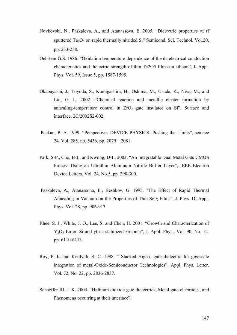
147
Novkovski, N., Paskaleva, A., and Atanassova, E. 2005. “Dielectric properties of rf
sputtered Ta2O5 on rapid thermally nitrided Si” Semicond. Sci. Technol. Vol.20,
pp. 233-238.
Oehrlein G.S. 1986. “Oxidation temperature dependence of the dc electrical conduction
characteristics and dielectric strength of thin Ta2O5 films on silicon”, J. Appl.
Phys. Vol. 59, Issue 5, pp. 1587-1595.
Okabayashi, J., Toyoda, S., Kumigashira, H., Oshima, M., Usuda, K., Niva, M., and
Liu, G. L. 2002. “Chemical reaction and metallic cluster formation by
annealing-temperature control in ZrO2 gate insulator on Si”, Surface and
interface. 2C/2002S2-002.
Packan, P. A. 1999. “Perspectives DEVICE PHYSICS: Pushing the Limits”, science
24. Vol. 285. no. 5436, pp. 2079 – 2081.
Park, S-P., Cho, B-J., and Kwong, D-L. 2003, “An Integratable Dual Metal Gate CMOS
Process Using an Ultrathin Aluminum Nitride Buffer Layer”, IEEE Electron
Device Letters. Vol. 24, No.5, pp. 298-300.
Paskaleva, A., Atanassona, E., Beshkov, G. 1995. "The Effect of Rapid Thermal
Annealing in Vacuum on the Properties of Thin SiO2 Films", J. Phys. D: Appl.
Phys. Vol. 28, pp. 906-913.
Rhee, S. J., White, J. O., Lee, S. and Chen, H. 2001. “Growth and Characterization of
Y2O3 Eu on Si and yttria-stabilized zirconia”, J. Appl. Phys., Vol. 90, No. 12.
pp. 6110-6113.
Roy, P. K.,and Kizilyali, S. C. 1998. “ Stacked High-ε gate dielectric for gigascale
integration of metal-Oxide-Semiconductor Technologies”, Appl. Phys. Letter.
Vol. 72, No. 22, pp. 2836-2837.
Schaeffer III, J. K. 2004. “Hafnium dioxide gate dielectrics, Metal gate electrodes, and
Phenomena occurring at their interface”.
148
Schroder, D. K. 1998. “Semiconductor Material and Device Characterization”, 2nd ed.,
John Wiley & Sons, New York .
Schulz M. and Johnson, N. M. 1977. “Transient capacitance measurements of hole
emission from interface states in MOS structures,” Appl. Phys. Letter. Vol. 31,
p. 622.
Shinriki, H. Kisu, T., Kimura, S-I., Nishioka, Y., Kawamoto, Y., and Mukai, K. 1990.
“Promising Storage Capacitor Structures with Thin Ta205 Film for Low-Power
High-Density DRAM’s”, IEEE Transactions on electronic Devices.Vol. 37, No.
9. pp. 1939-1947.
Shinriki, H., Nakata, M., Nishioka Y., and Mukai, K. 1989. “Two-step Annealing
Technique for Leakage Current Reduction in Chemical-Vapor-Deposited Ta205
Film” IEEE Electron Device Letters. Vol. 10, No. 11.pp.514-516.
Sjöblom, G., Westlinder, J., and Olsson, J. 2005. “Investigation of the thermal stability
of reactively sputter-deposited TiN MOS gate electrodes” IEEE Trans. electron
devices. Vol. 52, No. 10, pp. 2349-2352.
Spassov, D., Atanassova, E., Beshkov, G. 2000. “Effects of rapid thermal annealing in
vacuum on electrical properties of thin Ta2O5-Si structures” Microelectronics
Journal. Vol.31, P. 653-661.
Sun, S. C., and Chen, T. F. 1996. “ Leakage current reduction in Chemical-Vapor-
Deposited Ta2O5 film by rapid thermal annealing in N2O”, IEE Electron device
letters. Vol.17, No.7, pp. 355-357.
Tai, C-Y., Wilkinson, J. S., Perney, N. M. B., Netti, M. C., Cattaneo, F., Finlayson, C.
E., and Baumberg, J. J. 2004. “Determination of nonlinear refractive index in a
Ta2O5 rib waveguide using self-phase modulation”, OPTICS EXPRESS. Vol.
12, No. 21, pp. 5110-5115.
149
Tepehan, F.Z., Ghodsi, F.E., Tepehan, G.G., Ozer N. 1997. “Determination of optical
properties of amorphous Ta2O5 films deposited by spin- and dip-coating
methods” Solar Energy Materials and Solar Cells. Vol. 46, No. 4, pp. 311-
321(11).
Terman, L. M. 1962. “An Investigation of Surface States at a Silicon/Silicon Oxide
Interface Employing Metal-Oxide-Silicon Diodes,” Solid-State Electron. Vol. 5,
p. 285.
Timp, G., Agarwal, A., Baumann, F. H., Buonanno, M., Cirelli, R., Donnelly, V.,
Foad, M., Grant, D., Green, M., Gossmann, H., Hillenius, S., Jackson, J.,
Jacobson, D., Kleiman, R., Kornblit, A., Klemens, F., Lee, J. T-C., Mansfield,
W., Moccio, S., Murrell, A., O'Malley, M., Rosamilia, J., Sapjeta, J., Silverman,
P., Sorsch, T., Tai, W. W., Tennant, D., Vuong, H., Weir, B. 1997. "Low
Leakage 1.5nm Ultra-thin gate oxides for Extremely High Performance sub-
100nm n-MOSFETs", IEDM Tech. Dig., pp. 930-932.
Todorova Z., Donkov, N., Risti , Z., Bundaleski, N., Petrovi , S., Petkov, M. 2006.
“Electrical and Optical Characteristics of Ta2O5 Thin Films Deposited by
Electron-Beam Vapor Deposition” Plasma Processes and Polymers. Vol.3,
issue.2, pp. 174 – 178.
Tredwell, T.J., and Viswanathan, C.R. 1980. “Determination of Interface State
Parameters in a MOS Capacitor by DLTS”, Solid-State Electron. vol. 23, p.
1171.
Wang, S. J., Lim, P. C., Huan, A. C. H., Liu, C. L.,. Chai, J. W., Chow, S. Y., Pan, J. S.,
Li, Q. and Ong, C. K. 2003. “Reaction of SiO2 with hafnium oxide in low
oxygen pressure”, Appl. Phys. Lett., Vol. 82, No. 13, Pp. 2047-2049.
WEB_1, 2006. Silicon Moore’s Law, Intel® website, (02. 02. 2006).
http://www.intel.com/research/silicon/mooreslaw.htm.

150
Westlinder, J., Sjöblom, G., Olsson, J. 2004. “Variable work function in MOS
capacitors utilizing nitrogen-controlled TiNX gate electrodes”, Microelectronic
Eng. Vol. 75, P. 389-396.
Wilk, G. D. and Wallace, R. M. 2000. “Hafnium and zirconium silicates for advanced
gate dielectrics”, Appl. Phys. Lett. , Journal of Appl. Phys. Vol.87, p. 484.
Wilk. G. D., Wallace, R. M., Anthony, J. M. 2001. “High-k Gate Dielectrics: Current
Status and Materials Properties considerations”, Journal of Applied Physics.
Vol. 89, No. 10, pp.5243-5275.
Wolf, S. 2002. “Silicon Processing for the VLSI Era: Deep-Submicron Process
Technology”, 1st ed., (Lattice Press, Sunset Beach, CA).
Wolf, S., and Tauber, R. N. 1986. “Silicon Processing for the VLSI Era: Process
Technology” Lattice Press, Sunset Beach, Vol. 1, 1st ed., Chap. 7 & 16.
Wristers, D., Han, L. K., Chen, T., Wang, H. H., and Kwong, D. L. 1996, “Degradation
of Oxynitride Gate Dielectric” Reliability Due to Boron Diffusion”, Appl. Phys.
Lett. Vol. 68, No. 2094.
Yoon, S.G., Kim, H.K., Kim, M.J., Lee, H.M., and Yoon, D.H. 2004. “Evolution of
residual stress and optical properties in Ta2O5 thin films deposited at different
substrate temperatures with ion-beam deposition” E-MRS Spring Meeting.
Yun, M., Kim, M-S., Ko, Y-D., Moon, T-H., Hong, J-H., Myoung, J-M., Yun, I.,
2005. “Effects of post-metallization annealing of high-K dielectric thin films
grown by MOMBE” Microelectronic Engineering. Vol. 77, pp. 48–54.
Zier, M., Oswald, S., Reiche, R., Kozlowska, M., Wetzig, K. 2004. “Interface
formation and reactions on Ta- Si and Ta-SiO2 interfaces studied by XPS and
ARXPS” Journal of electron spectroscopy and related phenomena. Vol.137,
No.140 pp.229–233.


![[library.iyte.edu.tr] - İYTE Kütüphanesi - Ana Sayfalibrary.iyte.edu.tr/tezler/master/makinamuh/T000515.pdf · 2012-01-05[library.iyte.edu.tr] - İYTE Kütüphanesi - Ana Sayfa](https://img.pdfslide.us/doc/110x75/5ab633697f8b9a1a048d927e/-iyte-ktphanesi-ana-sayfa-iyte-ktphanesi-ana-sayfa.jpg)