Embed Size (px)
Citation preview
This content has been downloaded from IOPscience. Please scroll down to see the full text.
Download details:
This content was downloaded by: mmrhmatiar
IP Address: 130.113.31.51
This content was downloaded on 15/02/2014 at 01:42
Please note that terms and conditions apply.
The effects of oxygen plasma and humidity on surface roughness, water contact angle and
hardness of silicon, silicon dioxide and glass
View the table of contents for this issue, or go to the journal homepage for more
2014 J. Micromech. Microeng. 24 035010
(http://iopscience.iop.org/0960-1317/24/3/035010)
Home Search Collections Journals About Contact us My IOPscience
Journal of Micromechanics and Microengineering
J. Micromech. Microeng. 24 (2014) 035010 (14pp) doi:10.1088/0960-1317/24/3/035010
The effects of oxygen plasma and humidityon surface roughness, water contact angleand hardness of silicon, silicon dioxideand glass
A U Alam, M M R Howlader and M J Deen
Department of Electrical and Computer Engineering, McMaster University, 1280 Main Street West,Hamilton, Ontario, L8S 4K1, Canada
E-mail: [email protected] and [email protected]
Received 10 September 2013, revised 18 December 2013Accepted for publication 8 January 2014Published 14 February 2014
AbstractFor heterogeneous integration in many More-than-Moore applications, surface preparation isthe key step to realizing well-bonded multiple substrates for electronics, photonics, fluidicsand/or mechanical components without a degradation in performance. Therefore, it is criticalto understand how various processing and environmental conditions affect their surfaceproperties. In this paper, we investigate the effects of oxygen plasma and humidity on somekey surface properties such as the water contact angle, roughness and hardness of threematerials: silicon (Si), silicon dioxide (SiO2) and glass, and their impact on bondability. Thelow surface roughness, high surface reactivity and high hydrophilicity of Si, SiO2 and glass atlower activation times can result in better bondability. Although, the surface reactivity ofplasma-ambient-humidity-treated Si and SiO2 is considerably reduced, their reduction ofroughness and increase of hydrophilicity may enable good bonding at low temperature heatingdue to augmented hydroxyl groups. The decrease of hardness of Si and SiO2 with increasedactivation time is attributed to higher surface roughness and the formation of amorphous layersof Si. While contact angle and surface roughness results show a correlation with bondability,the role of hardness on bondability requires further investigation.
Keywords: surface roughness, water contact angle, hardness, oxygen plasma bonding,humidity
(Some figures may appear in colour only in the online journal)
1. Introduction
A major challenge in the semiconductor industry isheterogeneous integration of multiple technologies foremerging health, environmental, transportation or securityapplications. In heterogeneous integration, it is critical thatthe surfaces of the various substrates to be integrated ontoa common platform be properly cleaned and activated.In fact, the surface of the substrates is one of the mostimportant factors controlling the physical, chemical, electro-optical and microfluidic properties of new lab-on-chip, sensingor medical diagnostic systems. For these new systems
in the More-than-Moore ITRS (International TechnologyRoadmap of Semiconductors) [1] scenario, diverse materialsincluding silicon (Si) [2], silicon dioxide (SiO2) [3] andPyrex glass [4] are commonly used for the assemblyof integrated heterogeneous systems. For example, theheterogeneous integration of silicon-based electronics withphotonics components [5, 6], MEMS components such aselectrokinetic pumps or cell processing modules, polymer-based filtration systems [7, 8], and silicon- or polymer-basedsensors with microfabricated reference electrodes [7, 9, 10],all require the bonding of one substrate to another. Examplesof commonly-used substrates include silicon, silicon dioxide
0960-1317/14/035010+14$33.00 1 © 2014 IOP Publishing Ltd Printed in the UK
J. Micromech. Microeng. 24 (2014) 035010 A U Alam et al
or glass, on which the electronics, photonics, MEMS orfluidic components or modules are fabricated and subsequentlyintegrated to create lab-on-chip sensing [7] or imaging [11]systems. For these MEMS-based applications, an importantrequirement of the bonding or integration technique is thatthe performance and reliability of the individual modulesshould not be compromised after bonding [12]. To maintainperformance and reliability, appropriate surface preparationbefore bonding is a key requirement.
Previously, various surface treatment techniques [13–18]have been utilized for their integration. One of the promisingtechniques is surface-activated bonding using oxygen reactiveion etching (O2RIE) plasma [18]. The O2RIE plasma modifiesthe hydrophilicity (i.e., contact angle), morphology (i.e.,surface roughness) and mechanical properties (e.g., surfacehardness) of the surfaces that affect the solid–solid interfacesin, for example, wafer bonding [19], and the solid–liquidinterfaces in miniaturized biomedical systems [20, 21].
Contact angle measurement is critical to identifying thehydrophilicity of the surfaces in systems’ integration. Forexample, in Si-based wafer bonding, an environment withhigh relative humidity containing OH groups resulted in alower contact angle or higher hydrophilicity [22]. Near-surfacenanohardness and contact angle measurements in plasmaimmersion ion implanted silicon wafers showed increasedreliability for high-temperature microelectronics [23]. Thesurface charge and contact angle (i.e., surface reactivity)of SiO2 films with argon (Ar) and H2O plasma treatmentsand their aging behavior were investigated [24]. The H2Oplasma-treated surfaces showed higher compositional stabilitythan that with Ar plasma treatment. Surface treatment usingplasma polymerization was used for the fabrication of organicmicrofluidic devices on silicon/glass substrate [17]. Thefluid velocity was increased up to 450 μm s−1 due tosurface modification with plasma polymerized acrylic acid.A constant surface reactivity of Si and glass in microfluidicdevices was achieved due to dichlorodimethylsilane chemicaltreatment [25]. Also, passive microfluidic valves weremade using SiO2/glass hydrophobic (contact angle ∼102◦)micro-channels modified by self-assembled monolayer ofoctadecyltrichlorosilane and plasma deposited CHF3 patterns[26].
The contact angle provides information about thechemical affinity of bonding surfaces. Surface roughnessand surface mechanical properties such as material elasticitydetermine the contact quality of the integrated systems. Forexample, surface roughness was considered in the calculationof adhesion for the real area of contact in the direct waferbonding [27]. In the laser bonding of Pyrex/Si, the bondingstrength decreased almost linearly with the increase of surfaceroughness [28]. A direct correlation of surface roughness withbonding strength was also found by the bearing ratio (i.e.,the ratio of the area above a given height to the total area)analysis of surface roughness. A decrease of effective bondstrength with decreasing bearing ratio was reported [28]. Inanother study, surface roughness was decreased with increasedtemperature during hydrazine (a chemical propellant forsatellites) treatment of Si/SiO2/Si3N4 passivation layer for a
hydrazine-based microthruster [29]. Also, surface topographyrelated to the fatigue of poly-Si under the application ofa wide range of cyclic voltages was studied. Nucleationand propagation of micro-cracks were observed. In fact, asurface smoothening effect was observed above a critical cyclicvoltage of ∼140 V [30]. In the study of the nanomechanicalproperties of standard and strained SOI, thin bonded Sifilms showed a considerably lower hardness and modulus ofelasticity than those of bulk single crystal Si [31]. Plasmaactivation techniques using NH3, O2 and H2 were used to tunethe hardness of SiO2 thin films [32].
Recently, we have demonstrated the surface-activatedbonding of Si/Ge, SiO2/Ge and glass/glass using O2RIE.The high hydrophilicity of the Si, Ge and SiO2 surfaceswere combined with their higher surface reactivity andlow surface roughness to attain good bonding [33, 34].But these results do not provide plasma activation timedependent surface hydrophilicity, morphology and hardness.The humidity induced hydrophilicity of silicon oxide resultingin degraded adhesion was reported [35]. Unfortunately, therole of the ambient and humidity storage on the surfaceshas not yet been investigated. Moreover, there is a need tocharacterize the surfaces that are to be processed in a singleresearch facility in order to avoid artifacts induced by theprocessing equipment. Thus a comprehensive investigation ofO2RIE plasma processed Si, SiO2 and glass through watercontact angle, surface roughness and hardness are needed.
This article investigates the influence of O2RIE plasmaand humidity on the water contact angle, roughness andhardness of Si, SiO2 and glass surfaces affecting theirbondability. To clarify the individual role of the plasmaand humidity, the plasma activated surfaces were treated indifferent sequences in a clean room ambient, and/or in ahumidity-reliability chamber at 15 ◦C and 98% RH. The watercontact angle, roughness and hardness of the O2RIE plasma-treated surfaces at different storage conditions were analyzedusing a drop shape analyzer, an atomic force microscope(AFM) and an ultra-micro hardness tester.
2. Materials and methods
2.1. Preparation of materials
Three types of materials were used for the surface analysis:(i) one-side mirror polished p-type Si(1 0 0) wafers of 450 μmthickness; (ii) SiO2-on-Si wafers with 50 nm thick thermaloxides; and (iii) glass (from SCHOTT, US) wafers. The as-received Si wafers have native oxides of thickness ∼2 nm [13].The wafers were cut into 10 × 10 mm2 pieces using diamondneedle. The O2RIE plasma activations were performed forthree sets of Si and SiO2 pieces. In each set, there werethree pieces of wafers for each activation time, which wereused for roughness, hardness and contact angle measurement,respectively. The plasma activation time ranged from 60 to1200 s. Although typical wafer bonding techniques [36] donot use such a high activation time for surface treatment,we utilized this large range in order to clearly identify theeffect of plasma activation on other bonding parameters
2
J. Micromech. Microeng. 24 (2014) 035010 A U Alam et al
Table 1. Description of the materials, their surface activation and storage conditions with their corresponding acronyms.
Acronyms Surface activation Storage conditions Materials
Si:O2RIE O2RIE plasma No storage SiSi:O2RIE+20RH O2RIE plasma 20 days of storage in 98% RH and 15 ◦C temperature SiSi:O2RIE:20D+20RH O2RIE plasma 20 days of storage in class 1000 cleanroom ambient and Si
20 days in 98% RH and 15 ◦C temperatureSiO2:O2RIE O2RIE plasma No storage SiO2
SiO2:O2RIE+20RH O2RIE plasma 20 days of storage in 98% RH and 15 ◦C temperature SiO2
SiO2:O2RIE+20D+20RH O2RIE plasma 20 days of storage in class 1000 cleanroom ambient and SiO2
20 days in 98% RH and 15 ◦C temperatureGlass:O2RIE O2RIE plasma No storage Glass
(i.e., hydrophilicity, roughness and hardness). Table 1 showsthe three sets of Si and SiO2 specimens and one set of glassspecimens along with their activation time, storage conditionsand acronyms. The first set of wafers was analyzed right afterthe O2RIE plasma activation. The second set was analyzedafter storing in 98% relative humidity for 20 days. The third setwas analyzed after storing in clean room ambient (class 1000,23 ◦C and 45% RH) for 20 days as well as for 20 days in 15 ◦Ctemperature and 98% relative humidity to investigate theirstorage behavior. In the case of glass, there was only one set ofwafers. It was analyzed right after the plasma activation. Thesehumidity and ambient conditions were chosen to identify theaging processes [37] in the surfaces that control the bondingand packaging of MEMS. The temperature of the humiditychamber was held at 15 ◦C to achieve the highest humidity. Inorder to denote different sets of wafers with different activationtimes and storage conditions, we will use the acronyms definedin the following.
2.2. Oxygen plasma activation
The wafer surfaces were activated in a low vacuum pressureusing a 13.85 MHz oxygen O2RIE plasma in a hybridplasma bonder (HPB) from the BondtechTM Corporation. Moredetails about the oxygen RIE plasma generation are providedelsewhere [18]. The different plasma activation times selectedwere 60 s, 150 s, 300 s, 600 s and 1200 s. The plasma powerwas 300 W and the pressure during plasma glow was 200 Pa.
2.3. Atomic force microscopy (AFM)
The surface roughness was measured using a dimension iconAFM from the Bruker Corporation. A Si RTSPA tip was usedin standard tapping mode with a scan area of 2 × 2 μm2.The surface roughness (Rq) was measured using the root meansquare (RMS) method. Other roughness parameters such asmaximum height (Rz), skewness (Sku) and kurtosis (Rku) werealso measured.
2.4. Contact angle measurement
The water contact angle was measured using a drop shapeanalysis system (DSA100) from KRUSS with a 6 μl de-ionizedwater droplet. The contact angle measurement of the first set ofwafers after O2RIE activation was delayed for approximately3 min due to the transfer of specimens from the HPB to theDSA100 workstation. The sessile drop method [38] was used
for the contact angle measurements. The contact angles ofeach specimen were measured once every second for 2 min ofelapsed time to get an average contact angle.
2.5. Martens’ hardness measurement
The Martens’ hardness of surfaces was measured using aSHIMADZU Dynamic Ultra-micro Hardness Tester (DUH-211S). A triangular pyramid indenter with a tip angle of 115◦
was used. The Martens’ hardness is calculated from the appliedtest force versus indentation depth curve when increasing thetest force, using the following formula [39]:
HM = 1000F
26.43 × h2[Unit: N/mm−2],
where F = applied test force (mN) and h = indentation depth(μm). Two types of tests were conducted for the hardnessmeasurement, load–unload test and cycle test. In the load–unload test mode, the indenter force is increased to a presetmaximum force, held at this force for a specified time and thenthe indenter is unloaded. The cycle test indentation experimentconsists of several steps, such as approaching the surface;loading to maximum force; holding the force for a specifiedtime; unloading to minimum force; reloading to peak forceagain; holding the force again; and so on. The preset maximumtest force for both the load–unload test and the cycle test was10 mN. In the cycle test, the number of cycles was five. Thereason for using a very low test force was to measure thenanoindentation hardness, which is related to only the treatedsurface and where the size of the residual impression is oftenonly a few microns [40].
2.6. Humidity and reliability chamber
Specimens were stored in a humidity-reliability chamber fromESPEC. The temperature and relative humidity was heldconstant at 15 ◦C and 98% RH. The temperature and humidityrange of the chamber was −35 to 180 ◦C and 10% to 98%RH. The temperature accuracy was ± 0.3 ◦C, and that of thehumidity was ± 2.5% RH.
3. Results and discussions
3.1. Surface roughness
Figures 1 and 2 show the typical three-dimensional (3D)AFM images of Si and SiO2 wafer surfaces before and after
3
J. Micromech. Microeng. 24 (2014) 035010 A U Alam et al
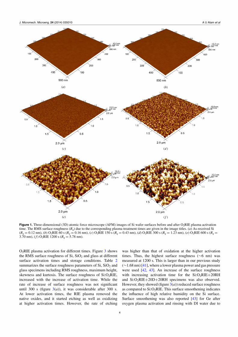
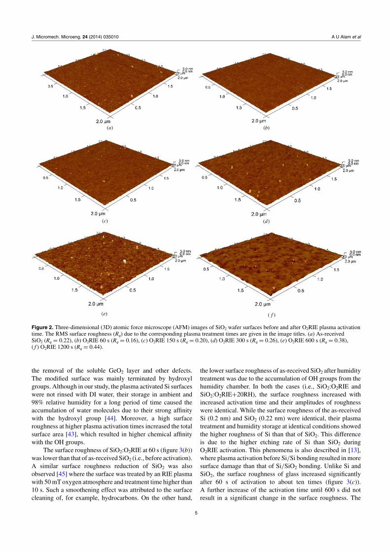
Figure 1. Three-dimensional (3D) atomic force microscope (AFM) images of Si wafer surfaces before and after O2RIE plasma activationtime. The RMS surface roughness (Rq) due to the corresponding plasma treatment times are given in the image titles. (a) As-received Si(Rq = 0.12 nm), (b) O2RIE 60 s (Rq = 0.16 nm), (c) O2RIE 150 s (Rq = 0.43 nm), (d) O2RIE 300 s (Rq = 1.23 nm), (e) O2RIE 600 s (Rq =3.70 nm), ( f ) O2RIE 1200 s (Rq = 5.78 nm).
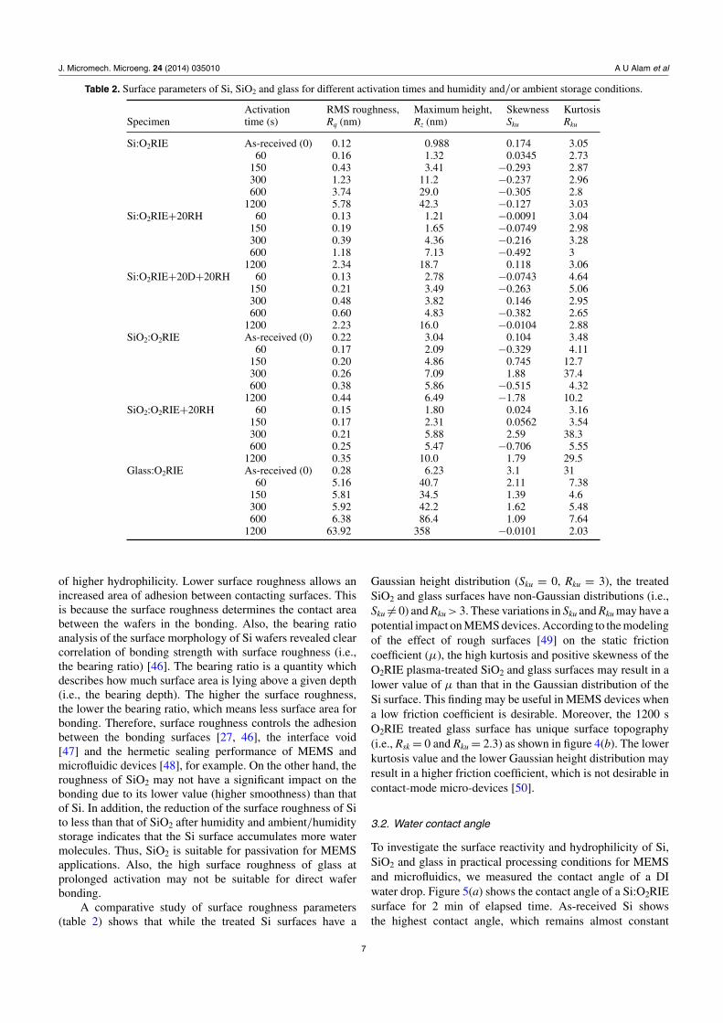
O2RIE plasma activation for different times. Figure 3 showsthe RMS surface roughness of Si, SiO2 and glass at differentsurface activation times and storage conditions. Table 2summarizes the surface roughness parameters of Si, SiO2 andglass specimens including RMS roughness, maximum height,skewness and kurtosis. The surface roughness of Si:O2RIE,increased with the increase of activation time. While therate of increase of surface roughness was not significantuntil 300 s (figure 3(a)), it was considerable after 300 s.At lower activation times, the RIE plasma removed thenative oxides, and it started etching as well as oxidizingat higher activation times. However, the rate of etching
was higher than that of oxidation at the higher activationtimes. Thus, the highest surface roughness (∼6 nm) wasmeasured at 1200 s. This is larger than in our previous study(∼1.68 nm) [41], where a lower plasma power and gas pressurewere used [42, 43]. An increase of the surface roughnesswith increasing activation time for the Si:O2RIE+20RHand Si:O2RIE+20D+20RH specimens was also observed.However, they showed (figure 3(a)) reduced surface roughnessas compared to Si:O2RIE. This surface smoothening indicatesthe influence of high relative humidity on the Si surface.Surface smoothening was also reported [43] for Ge afteroxygen plasma activation and rinsing with DI water due to
4
J. Micromech. Microeng. 24 (2014) 035010 A U Alam et al
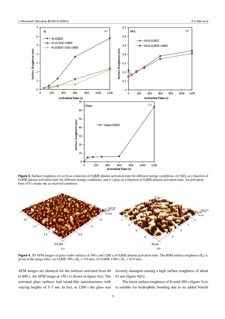
Figure 2. Three-dimensional (3D) atomic force microscope (AFM) images of SiO2 wafer surfaces before and after O2RIE plasma activationtime. The RMS surface roughness (Rq) due to the corresponding plasma treatment times are given in the image titles. (a) As-receivedSiO2 (Rq = 0.22), (b) O2RIE 60 s (Rq = 0.16), (c) O2RIE 150 s (Rq = 0.20), (d) O2RIE 300 s (Rq = 0.26), (e) O2RIE 600 s (Rq = 0.38),( f ) O2RIE 1200 s (Rq = 0.44).
the removal of the soluble GeO2 layer and other defects.The modified surface was mainly terminated by hydroxylgroups. Although in our study, the plasma activated Si surfaceswere not rinsed with DI water, their storage in ambient and98% relative humidity for a long period of time caused theaccumulation of water molecules due to their strong affinitywith the hydroxyl group [44]. Moreover, a high surfaceroughness at higher plasma activation times increased the totalsurface area [43], which resulted in higher chemical affinitywith the OH groups.
The surface roughness of SiO2:O2RIE at 60 s (figure 3(b))was lower than that of as-received SiO2 (i.e., before activation).A similar surface roughness reduction of SiO2 was alsoobserved [45] where the surface was treated by an RIE plasmawith 50 mT oxygen atmosphere and treatment time higher than10 s. Such a smoothening effect was attributed to the surfacecleaning of, for example, hydrocarbons. On the other hand,
the lower surface roughness of as-received SiO2 after humiditytreatment was due to the accumulation of OH groups from thehumidity chamber. In both the cases (i.e., SiO2:O2RIE andSiO2:O2RIE+20RH), the surface roughness increased withincreased activation time and their amplitudes of roughnesswere identical. While the surface roughness of the as-receivedSi (0.2 nm) and SiO2 (0.22 nm) were identical, their plasmatreatment and humidity storage at identical conditions showedthe higher roughness of Si than that of SiO2. This differenceis due to the higher etching rate of Si than SiO2 duringO2RIE activation. This phenomena is also described in [13],where plasma activation before Si/Si bonding resulted in moresurface damage than that of Si/SiO2 bonding. Unlike Si andSiO2, the surface roughness of glass increased significantlyafter 60 s of activation to about ten times (figure 3(c)).A further increase of the activation time until 600 s did notresult in a significant change in the surface roughness. The
5
J. Micromech. Microeng. 24 (2014) 035010 A U Alam et al
(a)
(c)
(b)
Figure 3. Surface roughness of (a) Si as a function of O2RIE plasma activation time for different storage conditions, (b) SiO2 as a function ofO2RIE plasma activation time for different storage conditions, and (c) glass as a function of O2RIE plasma activation time. An activationtime of 0 s means the as-received condition.
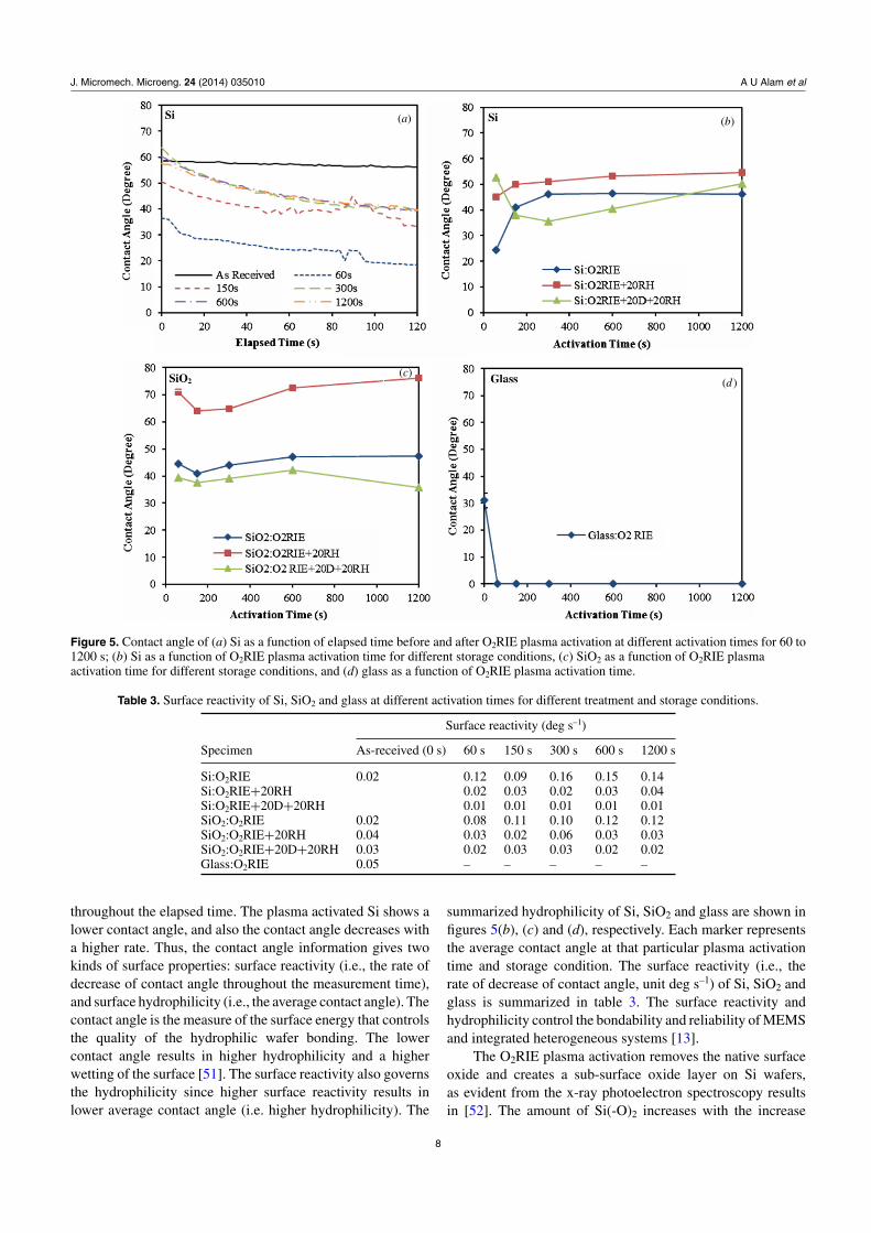
Figure 4. 3D AFM images of glass wafer surfaces at 300 s and 1200 s of O2RIE plasma activation time. The RMS surface roughness (Rq) isgiven in the image titles. (a) O2RIE 300 s (Rq = 5.9 nm), (b) O2RIE 1200 s (Rq = 63.9 nm).
AFM images are identical for the surfaces activated from 60
to 600 s. An AFM image at 150 s is shown in figure 4(a). The
activated glass surfaces had island-like nanostructures with
varying heights of 5–7 nm. In fact, at 1200 s the glass was
severely damaged causing a high surface roughness of about
63 nm (figure 4(b)).
The lower surface roughness of Si until 300 s (figure 3(a))
is suitable for hydrophilic bonding due to its added benefit
6
J. Micromech. Microeng. 24 (2014) 035010 A U Alam et al
Table 2. Surface parameters of Si, SiO2 and glass for different activation times and humidity and/or ambient storage conditions.
Activation RMS roughness, Maximum height, Skewness KurtosisSpecimen time (s) Rq (nm) Rz (nm) Sku Rku
Si:O2RIE As-received (0) 0.12 0.988 0.174 3.0560 0.16 1.32 0.0345 2.73
150 0.43 3.41 −0.293 2.87300 1.23 11.2 −0.237 2.96600 3.74 29.0 −0.305 2.8
1200 5.78 42.3 −0.127 3.03Si:O2RIE+20RH 60 0.13 1.21 −0.0091 3.04
150 0.19 1.65 −0.0749 2.98300 0.39 4.36 −0.216 3.28600 1.18 7.13 −0.492 3
1200 2.34 18.7 0.118 3.06Si:O2RIE+20D+20RH 60 0.13 2.78 −0.0743 4.64
150 0.21 3.49 −0.263 5.06300 0.48 3.82 0.146 2.95600 0.60 4.83 −0.382 2.65
1200 2.23 16.0 −0.0104 2.88SiO2:O2RIE As-received (0) 0.22 3.04 0.104 3.48
60 0.17 2.09 −0.329 4.11150 0.20 4.86 0.745 12.7300 0.26 7.09 1.88 37.4600 0.38 5.86 −0.515 4.32
1200 0.44 6.49 −1.78 10.2SiO2:O2RIE+20RH 60 0.15 1.80 0.024 3.16
150 0.17 2.31 0.0562 3.54300 0.21 5.88 2.59 38.3600 0.25 5.47 −0.706 5.55
1200 0.35 10.0 1.79 29.5Glass:O2RIE As-received (0) 0.28 6.23 3.1 31
60 5.16 40.7 2.11 7.38150 5.81 34.5 1.39 4.6300 5.92 42.2 1.62 5.48600 6.38 86.4 1.09 7.64
1200 63.92 358 −0.0101 2.03
of higher hydrophilicity. Lower surface roughness allows anincreased area of adhesion between contacting surfaces. Thisis because the surface roughness determines the contact areabetween the wafers in the bonding. Also, the bearing ratioanalysis of the surface morphology of Si wafers revealed clearcorrelation of bonding strength with surface roughness (i.e.,the bearing ratio) [46]. The bearing ratio is a quantity whichdescribes how much surface area is lying above a given depth(i.e., the bearing depth). The higher the surface roughness,the lower the bearing ratio, which means less surface area forbonding. Therefore, surface roughness controls the adhesionbetween the bonding surfaces [27, 46], the interface void[47] and the hermetic sealing performance of MEMS andmicrofluidic devices [48], for example. On the other hand, theroughness of SiO2 may not have a significant impact on thebonding due to its lower value (higher smoothness) than thatof Si. In addition, the reduction of the surface roughness of Sito less than that of SiO2 after humidity and ambient/humiditystorage indicates that the Si surface accumulates more watermolecules. Thus, SiO2 is suitable for passivation for MEMSapplications. Also, the high surface roughness of glass atprolonged activation may not be suitable for direct waferbonding.
A comparative study of surface roughness parameters(table 2) shows that while the treated Si surfaces have a
Gaussian height distribution (Sku = 0, Rku = 3), the treatedSiO2 and glass surfaces have non-Gaussian distributions (i.e.,Sku �= 0) and Rku > 3. These variations in Sku and Rku may have apotential impact on MEMS devices. According to the modelingof the effect of rough surfaces [49] on the static frictioncoefficient (μ), the high kurtosis and positive skewness of theO2RIE plasma-treated SiO2 and glass surfaces may result in alower value of μ than that in the Gaussian distribution of theSi surface. This finding may be useful in MEMS devices whena low friction coefficient is desirable. Moreover, the 1200 sO2RIE treated glass surface has unique surface topography(i.e., Rsk = 0 and Rku = 2.3) as shown in figure 4(b). The lowerkurtosis value and the lower Gaussian height distribution mayresult in a higher friction coefficient, which is not desirable incontact-mode micro-devices [50].
3.2. Water contact angle
To investigate the surface reactivity and hydrophilicity of Si,SiO2 and glass in practical processing conditions for MEMSand microfluidics, we measured the contact angle of a DIwater drop. Figure 5(a) shows the contact angle of a Si:O2RIEsurface for 2 min of elapsed time. As-received Si showsthe highest contact angle, which remains almost constant
7
J. Micromech. Microeng. 24 (2014) 035010 A U Alam et al
(a) (b)
(c)(d )
Figure 5. Contact angle of (a) Si as a function of elapsed time before and after O2RIE plasma activation at different activation times for 60 to1200 s; (b) Si as a function of O2RIE plasma activation time for different storage conditions, (c) SiO2 as a function of O2RIE plasmaactivation time for different storage conditions, and (d) glass as a function of O2RIE plasma activation time.
Table 3. Surface reactivity of Si, SiO2 and glass at different activation times for different treatment and storage conditions.
Surface reactivity (deg s–1)
Specimen As-received (0 s) 60 s 150 s 300 s 600 s 1200 s
Si:O2RIE 0.02 0.12 0.09 0.16 0.15 0.14Si:O2RIE+20RH 0.02 0.03 0.02 0.03 0.04Si:O2RIE+20D+20RH 0.01 0.01 0.01 0.01 0.01SiO2:O2RIE 0.02 0.08 0.11 0.10 0.12 0.12SiO2:O2RIE+20RH 0.04 0.03 0.02 0.06 0.03 0.03SiO2:O2RIE+20D+20RH 0.03 0.02 0.03 0.03 0.02 0.02Glass:O2RIE 0.05 – – – – –
throughout the elapsed time. The plasma activated Si shows alower contact angle, and also the contact angle decreases witha higher rate. Thus, the contact angle information gives twokinds of surface properties: surface reactivity (i.e., the rate ofdecrease of contact angle throughout the measurement time),and surface hydrophilicity (i.e., the average contact angle). Thecontact angle is the measure of the surface energy that controlsthe quality of the hydrophilic wafer bonding. The lowercontact angle results in higher hydrophilicity and a higherwetting of the surface [51]. The surface reactivity also governsthe hydrophilicity since higher surface reactivity results inlower average contact angle (i.e. higher hydrophilicity). The
summarized hydrophilicity of Si, SiO2 and glass are shown infigures 5(b), (c) and (d), respectively. Each marker representsthe average contact angle at that particular plasma activationtime and storage condition. The surface reactivity (i.e., therate of decrease of contact angle, unit deg s–1) of Si, SiO2 andglass is summarized in table 3. The surface reactivity andhydrophilicity control the bondability and reliability of MEMSand integrated heterogeneous systems [13].
The O2RIE plasma activation removes the native surfaceoxide and creates a sub-surface oxide layer on Si wafers,as evident from the x-ray photoelectron spectroscopy resultsin [52]. The amount of Si(-O)2 increases with the increase
8
J. Micromech. Microeng. 24 (2014) 035010 A U Alam et al
in plasma activation time for Si:O2RIE. The high surfacereactivity of Si:O2RIE (table 3) as compared to as-receivedSi is due to the removal of the native oxides and organiccontaminants and the increased number of dangling bonds(free bonds) from broken Si-O and Si-H [51]. Similarsurface reactivity behavior is also observed in the case ofSiO2:O2RIE (table 3). The increased surface reactivity alsoleads to higher surface energy and hence increased adhesionand bonding strength in plasma bonded wafers [53]. Thesurface reactivity of SiO2:O2RIE is slightly lower than thatof Si:O2RIE, indicating the high bonding strength of Si-basedwafer bonding [13, 54]. The glass: O2RIE showed the highestsurface reactivity, which makes it a promising candidate foranodic bonding [42]. The DI water drop quickly spread onthe O2RIE plasma-processed glass surface, which resultedin a contact angle that was below the measurement limitof the equipment. Storage in humidity (i.e., O2RIE+20RH)and ambient/humidity (i.e., O2RIE+20D+20RH) shows asignificant reduction in the surface reactivity of Si andSiO2 (table 3) due to the augmented -OH groups on the surface[41]. It has also been reported [43] that the surface reactivityof Si and SiO2 are at a maximum immediately after the plasmaactivation, even though they remain hydrophilic in excess of150 h after plasma activation. The highly reactive surfaceattracts particles from air when exposed in the ambient fora long period of time, which eventually decreases its surfacereactivity as well as hydrophilicity.
The contact angles of as-received Si (figure 5(a)) andSiO2 are almost identical (∼57◦), and are higher than thatof as-received glass (30◦, figure 5(d)). Glass:O2RIE showsthe highest hydrophilicity (contact angle <5◦) and Si:O2RIEshows higher hydrophilicity (24.5◦) than that of SiO2:O2RIEat 60 s. The contact angle values in this study vary slightlyfrom other studies due to different plasma powers, activationtimes, chamber pressures and atmospheric exposure times. Ina previous study, the contact angle of as-received SiO2 wasreported as 52◦ with a 9 μl DI water droplet, and the contactangle for O2RIE plasma activated Si and SiO2 was reported as29.1◦ and 38.5◦, respectively, with a flow rate of 50 sccm, apower of 200 W, a chamber pressure of 60 Pa and a plasmatreatment time of 30 s [33]. In another study, the contact angleof oxygen plasma-treated glass was <5◦ at a plasma power of140 W, a working pressure of 20 mTorr and a 60 s activationtime [42].
With increasing activation time, the contact angle of Siincreased until 300 s, and it became saturated at 600 s (46.5◦)and 1200 s (46.2◦). This is due to the increased surfaceroughness (see discussion in section 3.1) of Si:O2RIE at higheractivation times. Surface roughness obstructs the spreading ofa water droplet in the contact angle measurements. A highersurface roughness creates a larger barrier to the spreading ofwater, a higher surface area in a smaller lateral space and moreinteraction with surrounding air, resulting in a larger contactangle and vice versa [36]. On the other hand, the contact angleof SiO2:O2RIE does not change significantly with activationtime (figure 5(c)). The highly passivated SiO2 layer is lesslikely to react with oxygen plasma. The highly hydrophilicsurfaces form networks of hydrogen-bonded water molecules
between the contacted wafers, which in turn creates Si-O-Sibonds resulting in enhanced bond strength [22]. Thus, thelower activation times of Si: O2RIE can thus result in agood bonding strength due to the higher hydrophilicity andreactivity of the surface (figure 5(b)). On the other hand, highercontact angles in the case of Si:O2RIE+20RH (figure 5(b)) andSiO2:O2RIE+20RH (figure 5(c)) reflect their reduced surfacereactivity and less hydrophilicity due to the passivation of thedangling bonds.
The initial decrease of the contact angle ofSi:O2RIE+20D+20RH until 300 s and its increase afterwards(figure 5(b)) is attributed to the surface roughness inducedvariation in the amount of Si-(OH)x bonds [52]. Moreover,the decrease in contact angle for SiO2:O2RIE+20D+20RH(figure 5(c)) compared to that of SiO2:O2RIE was due toincreased incorporation with OH groups from humidity andambient. Thus Si and SiO2 need proper passivation to reducethe risks of poor adhesion due to humidity-induced increasedhydrophilicity in MEMS packaging [35]. Also, storage inambient and humidity can result in good bondability (i.e.,bonding strength), since the gap closing mechanism in roomtemperature direct wafer bonding requires water vapor fromthe ambient to initiate covalent bonding between the surfaces[55]. For further enhancement of bonding strength, a lowtemperature (i.e., 300 ◦C) heating for a short period of time(i.e., 2 h) was reported [41, 55]. The findings here canalso be extended to the sequential plasma activated bonding(O2RIE+nitrogen radicals) of Si/Si [51], Si/Pyrex glass [42],glass/glass [34], Si/Ge and SiO2/Ge [33].
3.3. Surface hardness
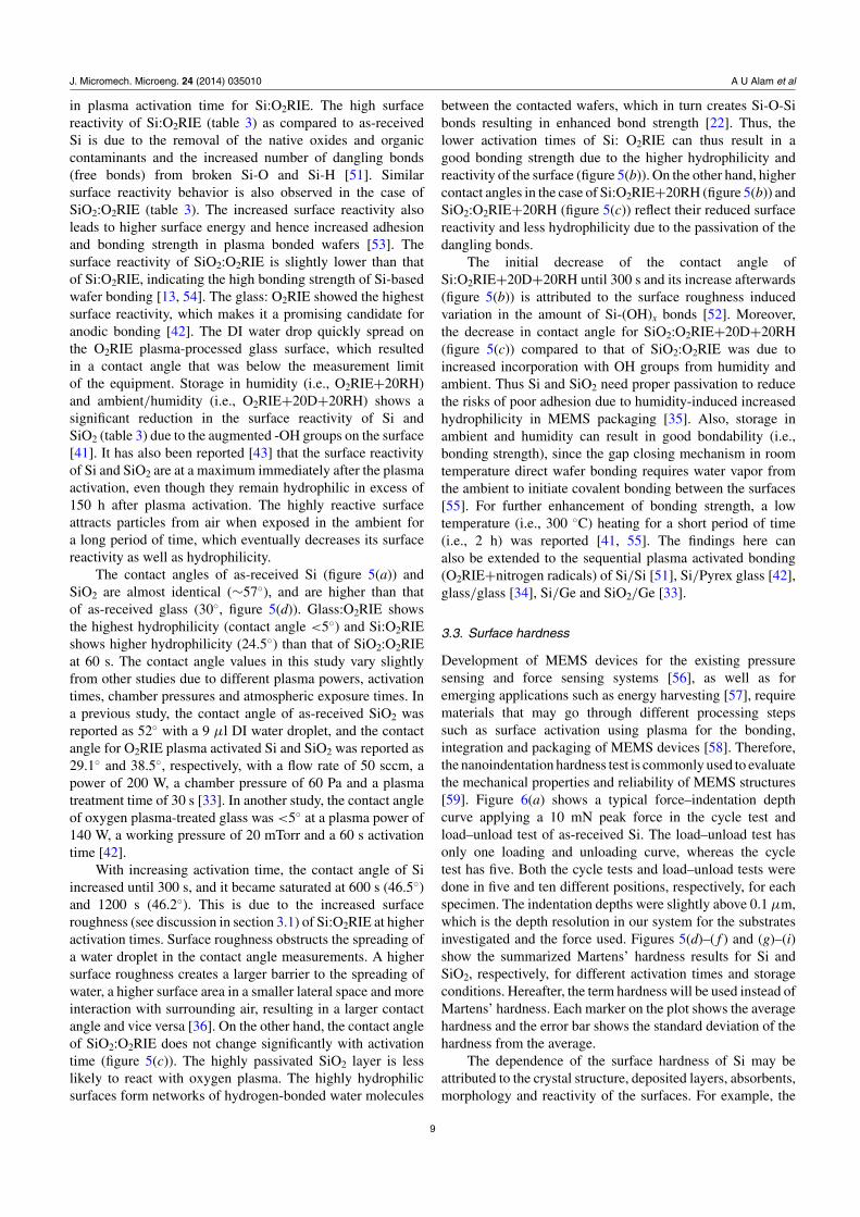
Development of MEMS devices for the existing pressuresensing and force sensing systems [56], as well as foremerging applications such as energy harvesting [57], requirematerials that may go through different processing stepssuch as surface activation using plasma for the bonding,integration and packaging of MEMS devices [58]. Therefore,the nanoindentation hardness test is commonly used to evaluatethe mechanical properties and reliability of MEMS structures[59]. Figure 6(a) shows a typical force–indentation depthcurve applying a 10 mN peak force in the cycle test andload–unload test of as-received Si. The load–unload test hasonly one loading and unloading curve, whereas the cycletest has five. Both the cycle tests and load–unload tests weredone in five and ten different positions, respectively, for eachspecimen. The indentation depths were slightly above 0.1 μm,which is the depth resolution in our system for the substratesinvestigated and the force used. Figures 5(d)–( f ) and (g)–(i)show the summarized Martens’ hardness results for Si andSiO2, respectively, for different activation times and storageconditions. Hereafter, the term hardness will be used instead ofMartens’ hardness. Each marker on the plot shows the averagehardness and the error bar shows the standard deviation of thehardness from the average.
The dependence of the surface hardness of Si may beattributed to the crystal structure, deposited layers, absorbents,morphology and reactivity of the surfaces. For example, the
9
J. Micromech. Microeng. 24 (2014) 035010 A U Alam et al
(a) (d) (g)
(c) (f) (i)
(b) (e) ( h)
Figure 6. Indenter force versus indentation depth of (a) as-received Si, (b) as-received SiO2, and (c) as-received glass, in the cycle test andthe load–unload test for the analysis of Martens’ hardness. Martens’ hardness using the cycle test and the load–unload test as a function ofO2RIE plasma activation time for (d) Si without storing, (e) Si after storing in 98% relative humidity for 20 days, and ( f ) Si after storing inambient for 20 days and in 98% relative humidity for 20 days, (g) SiO2 without storing, (h) SiO2 after storing in 98% relative humidity for20 days, and (i) SiO2 after storing in ambient for 20 days and in 98% relative humidity for 20 days.
loading–unloading process in the cycle test for as-received Si(figure 6(a)) shows hysteresis. It could be due to a pressure-induced phase transformation [49] of Si from diamond cubicform into β-tin form with a 22% decrease in volume. Sincethe surface roughness of the as-received Si and Si:O2RIE
at 60 s are identical, the lower hardness for the as-receivedSi (figure 6(d)) may be attributed to the native oxides andcontaminants. Alternatively, the increase in hardness at 60 s isdue to the removal of the native oxides. On the other hand, ifonly the lower deviation is considered at 150 s of Si:O2RIE,
10
J. Micromech. Microeng. 24 (2014) 035010 A U Alam et al
Table 4. Evolution of surface properties with the increase of oxygen plasma activation times at different storage conditions.
Change in surface properties with the increase of activation times (60, 150, 300, and 600 s)under different storage conditions
Surface SurfaceSurface treatment roughness reactivity Hydrophilicity Hardness Bondability
Si:O2RIE Increases High High Decreases Better at lower activation time [41]Si:O2RIE+20RH Slower increase Low Low Slight decrease Good at lower activation
than Si:O2RIESi:O2RIE+20D+20RH Similar to Very low High Overall decrease Good at lower activation
Si:O2RIE+20RHSiO2:O2RIE Slight increase High High Decreases Better at lower activation timeSiO2:O2RIE+20RH Similar to Low Low Slight decreases Better at lower activation time
SiO2:O2RIESiO2:O2RIE+20D+20RH – Very low High Overall decrease Good at lower activationGlass:O2RIE ∼ 5–10 nm Very high Very high Negligible change Better at low activation time
a decreasing trend in the hardness of Si is observed with theincrease in activation time both in the cycle test and the load–unload test. This decrease could be related to higher surfaceroughness and changes in the atomic structure of the surfaces.The hardness of the plasma-induced oxide layers or the nativeoxide layers of Si wafers is below the measurement limitof the nanoindentation test equipment. The equipment canresolve a minimum depth of 0.1 μm (i.e., 100 nm), whereasthe native oxide and sub-surface oxide layers are in the order ofseveral nanometers. Thus the nanoindentation tests provide thehardness of surface/sub-surface oxide layers combined withthe bulk material [60].
As discussed in the previous section, the surfaceroughness of Si increases with the increase of activationtime. Therefore, higher surface roughness results in a lowercontact area of the indenter tip, which causes an increasein the indentation depth observed in the depth versus forceprofiles. The indentation depth for the as-received Si and atlow activation times (i.e., 60 s and 150 s) is lower (∼0.26 μm)than that (∼0.30 μm) of the higher activation times (i.e., 600 sand 1200 s). Therefore, the surface roughness controls thehardness of Si. It is also known that surface treatment usingplasma having enough physical sputtering capability results inan amorphous layer [61]. The decrease of the hardness withincreased activation time (figure 6(d)) may also be attributed tothe formation of amorphous layer at higher plasma activationtimes. The formation of an amorphous layer in the plasmasurface-activated wafer bonding was demonstrated elsewhere[62].
There was no considerable influence of humidity onthe hardness of Si:O2RIE+20RH (figure 6(e)). However,a decreasing trend in the hardness was observed in theload–unload test. Also, the rate of decrease of hardness forSi:O2RIE+20RH with an increased activation time was lowerthan that of Si:O2RIE in the load–unload test. Further storage inambient/humidity (i.e., Si:O2RIE+20D+20RH, figure 6( f ))caused a decrease in hardness (∼6000 to ∼3500 N mm−2) from60 to 150 s and an eventual increase up to ∼5000 N mm−2 at1200 s. The humidity, and the ambient/humidity storageinduced variation in the hardness, is attributed to the qualityof the complex formation of the absorbents (e.g., -OH) anddeposited layers (e.g., carbon) on the surface. The surface
reactivity determined by the relative composition of surfaceoxides due to hydroxyl groups (i.e., Si-OH) and sub-oxides(i.e., Si-O2, Si-O4) also may influence the hardness of Si.
The repeated force–indentation depth curves of the as-received SiO2 (figure 6(b)) show higher hysteresis than thatof Si (figure 6(a)). The hardness behavior of SiO2:O2RIEis identical to that of Si (figure 6(g)), except for its highervalues from 60 to 600 s and its lower value at 1200 s.For SiO2:O2RIE+20RH (figure 6(h)), the hardness decreasedexcept for 1200 s of activation time both in the load–unload test and the cycle test. On the other hand, forSiO2:O2RIE+20D+20RH (figure 6(i)), the hardness valuesin load–unload tests did not change significantly if only theupper deviation at 300 s was considered. Unlike Si, the surfaceroughness may not have a significant impact on the reductionof hardness, since SiO2 shows a small increase in surfaceroughness with increased activation time. The role of depositedoxides, hydroxyl layers/absorbents and surface reactivity onthe hardness of SiO2 is not clear from this study due to itshigher hardness than that of the surface additives. Unlike Siand SiO2, glass showed the least hysteresis (figure 6(c)). Also,the change in the hardness (∼4000 N mm−2, not shown infigure 6) of glass:O2RIE was insignificant with the increasein activation time except for at 1200 s, where it reduced toalmost half (∼2000 N mm−2). This reduction in the hardnessmay be attributed to the severe damage of the glass surfaceafter such a long activation time. The surface roughness ofglass for this condition increased by more than ten times thatof the as-received specimen.
A comparison among the O2RIE treated specimens(figures 5(d), (g) and Glass:O2RIE) shows that SiO2 hasthe highest hardness and glass has the lowest hardness foridentical conditions of activation time. The loading andunloading curves provide the plastic and elastic deformationof the surface [63]. Whereas, the as-received glass has anelasticity of ∼7.5 × 10⁴ N mm−2, the elasticity of the as-received Si and SiO2 surfaces is almost equal, and is about∼1.2 × 10⁵ N mm−2. Thus, the glass has a lower plasticdeformation compared to Si and SiO2. The lower plasticdeformation of glass makes it a good candidate material formicrofluidic devices with other polymer or flexible materials[64]. A comparison in the change of the surface properties of
11
J. Micromech. Microeng. 24 (2014) 035010 A U Alam et al
the specimens with increase in activation time is summarizedin table 4.
4. Conclusions
The water contact angle, roughness and hardness of oxygenreactive ion etching (O2RIE) plasma activated silicon(Si), silicon dioxide (SiO2) and glass surfaces with orwithout storage in ambient and 98% relative humiditywere investigated. The summarized surface properties of Si,SiO2 and glass are shown in table 4. The surface roughness forSi was increased with the increase of plasma activation timeand it was higher than that of SiO2. The surface roughnessof the activated Si was reduced after treating it with humidityand air, but no change was observed in the SiO2. This highlyreduced roughness was due to higher accumulation of watermolecules on Si surface. The surface roughness of glasssuddenly increased after activation by an order of magnitude,then remained unchanged until 600 s and finally increasedby another order of magnitude at 1200 s. This significantlyincreased roughness at 1200 s is due to surface damage. Thelow surface roughness at lower activation times is suitable forbonding.
The oxygen plasma activation of Si showed a lowercontact angle and it showed an increasing trend with increasingactivation time. Also, Si and SiO2 showed high surfacereactivity after plasma activation, which was considerablyreduced after storage in humidity and ambient. The contactangle of the plasma-activated Si and SiO2 surfaces wasdecreased due to the augmented -OH groups in ambient andhumidity. Moreover, plasma-activated glass showed a highlyreactive as well as hydrophilic surface that resulted in contactangles below 2◦, which is beyond the detection limit. The highhydrophilicty and surface reactivity at lower activation timescan result in better bondability. The high hydrophilicity afterhumidity–ambient treatment may also have good bondabilityprovided that the surface contains OH groups.
The loading–unloading results in the hardness test identifyhysteresis for Si, SiO2 and glass due to the pressure-inducedphase transformation. The hardness of Si and SiO2 wasdecreased with increased activation time due to the highersurface roughness and the formation of amorphous layers(of Si). A considerable reduction in the hardness of the plasma-activated glass at 1200 s was observed due to the highlyincreased surface roughness. Furthermore, the humidity, andambient/humidity storage induced variation was observed inSi and SiO2. This dependence of the hardness is thought to bedue to the quality of the complex formation of the absorbents(e.g., -OH), deposited layers (e.g., carbon), oxides (i.e., Si-OH)and sub-oxides (i.e., Si-O2, Si-O4) on the surface. Althougha high surface hardness is observed at a lower activationtime (i.e., high bondability region), the role of hardness onbondability needs further investigation.
Acknowledgments
This research is supported by discovery grants from theNatural Science and Engineering Research Council (NSERC)
of Canada, an infrastructure grant from the Canada Foundationfor Innovation (CFI), an Ontario Research Fund for ResearchExcellence (ORF-RE) Funding Grant and the Canada ResearchChair program. The authors gratefully acknowledge FangfangZhang for her help with Hybrid Plasma Bonder. Also, theauthors acknowledge to Professor M J Kim, University ofTexas at Dallas for his comments on preparation of the results.
References
[1] International Technology Roadmap for Semiconductors, 2012Update Overview www.itrs.net/links/2012ITRS/2012Chapters/2012overview.pdf
[2] Krauter G, Schumacher A and Gosele U 1998 Lowtemperature silicon direct bonding for application inmicromechanics: bonding energies for differentcombinations of oxides Sensors Actuators A 70 271–5
[3] Takagi H, Maeda R, Chung T R and Suga T 1998Low-temperature direct bonding of silicon and silicondioxide by the surface activation method Sensors ActuatorsA 70 164–70
[4] Wei J, Nai S M L, Wong C K and Lee L C 2004 Glass-to-glassanodic bonding process and electrostatic force Thin SolidFilms 462–3 487–91
[5] Deen M J and Basu P K 2012 Silicon photodetectors SiliconPhotonics: Fundamentals and Devices (Chichester: Wiley)DOI:10.1002/9781119945161.ch8
[6] Li Z, Deen M J, Fang Q and Selvaganapathy P R 2012 Designof a flat field concave-grating-based micro-Ramanspectrometer for environmental applications Appl. Opt.51 6855–63
[7] Shinwari M W, Deen M J and Landheer D 2007 Study of theelectrolyte-insulator-semiconductor field-effect transistor(EISFET) with applications in biosensor designMicroelectron. Reliab. 47 2025–57
[8] Howlader M M R, Zhang F and Deen M J 2013 Formation ofgallium arsenide nanostructures in Pyrex glassNanotechnology 24 315301
[9] Shinwari M W, Zhitomirsky D, Deen I A,Selvaganapathy P R, Deen M J and Landheer D 2010Microfabricated reference electrodes and their biosensingapplications Sensors 10 1679–715
[10] Safari S, Selvaganapathy P R and Deen M J 2013 Microfluidicreference electrode with free-diffusion liquid junctionJ. Electrochem. Soc. 160 B177–83
[11] Campos F S, Faramarzpour N, Marinov O, Deen M Jand Swart J W 2013 Photodetection with gate-controlledlateral BJTs from standard CMOS technology IEEE Sens. J.13 1554–63
[12] Howlader M M R, Selvaganapathy P R, Deen M J and Suga T2011 Nanobonding technology toward electronic, fluidic,and photonic systems integration IEEE J. Sel. Top.Quantum Electron. 17 689–703
[13] Suni T, Henttinen K, Suni I and Makinen J 2002 Effects ofplasma activation on hydrophilic bonding of Si and SiO2
J. Electrochem. Soc. 149 G348[14] Byun K Y, Ferain I and Colinge C 2010 Effect of free radical
activation for low temperature Si to Si wafer bondingJ. Electrochem. Soc. 157 H109
[15] Reiche M, Gosele U and Wiegand M 2000 Modification of Si(1 0 0)-surfaces by SF6 plasma etching – application towafer direct bonding Cryst. Res. Technol. 35 807–21
[16] Tang Z, Peng P, Shi T, Liao G, Nie L and Liu S 2009 Effect ofnanoscale surface topography on low temperature directwafer bonding process with UV activation SensorsActuators A 151 81–86
12
J. Micromech. Microeng. 24 (2014) 035010 A U Alam et al
[17] Dhayal M, Jeong H G and Choi J S 2005 Use of plasmapolymerisation process for fabrication of bio-MEMS formicro-fluidic devices Appl. Surf. Sci. 252 1710–5
[18] Howlader M M R, Kibria M G, Zhang F and Kim M J 2010Hybrid plasma bonding for void-free strong bondedinterface of silicon/glass at 200 ◦C Talanta 82 508–15
[19] Howlader M M R, Kagami G, Lee S H, Wang J G, Kim M Jand Yamauchi A 2010 Sequential plasma-activated bondingmechanism of silicon/silicon wafers J. Microelectromech.Syst. 19 840–8
[20] Li J, Cui Z and Baker M 2004 A study of the surfacechemistry, morphology and wear of silicon based MEMSSurf. Interface Anal. 36 1254–8
[21] Ardito R, Corigliano A and Frangi A 2009 On the analysis ofspontaneous adhesion in MEMS EuroSimE ‘09 : 10th Int.Conf. on Thermal, Mechanical and Multi-PhysicsSimulation and Experiments in Microelectronics andMicrosystems pp 1–7
[22] Tong Q-Y 1997 The role of surface chemistry in bonding ofstandard silicon wafers J. Electrochem. Soc. 144 384
[23] Ueda M, Lepienski C, Rangel E, Cruz N and Dias F 2002Nanohardness and contact angle of Si wafers implantedwith N and C and Al alloy with N by plasma ionimplantation Surf. Coat. Technol. 156 190–4
[24] Trevino K J, Shearer J C, Tompkins B D and Fisher E R 2011Comparing isoelectric point and surface composition ofplasma modified native and deposited SiO2 films usingcontact angle titrations and x-ray photoelectronspectroscopy Plasma Process. Polym. 8 951–64
[25] Christensen T B, Pedersen C M, Grondahl K G, Jensen T G,Sekulovic A, Bang D D and Wolff A 2007 PCRbiocompatibility of lab-on-a-chip and MEMS materialsJ. Micromech. Microeng. 17 1527–32
[26] Feng Y, Zhou Z, Ye X and Xiong J 2003 Passive valves basedon hydrophobic microfluidics Sensors Actuators A108 138–43
[27] Gui C, Elwenspoek M, Tas N and Gardeniers J G E 1999 Theeffect of surface roughness on direct wafer bonding J. Appl.Phys. 85 7448
[28] Tseng A A 2006 Effects of surface roughness and oxide layeron wafer bonding strength using transmission laser bondingtechnique ITHERM ‘06 : Therm. Thermomechanical Proc.10th Intersoc. Conf. Phenom. Electron. Syst pp 1349–57
[29] Kundu P, Ghosh A, Das S and Bhattacharyya T K 2012Compatibility study of thin passivation layers withhydrazine for silicon-based MEMS microthruster J. Phys.D. Appl. Phys. 45 095302
[30] Allameh S, Gally B, Brown S and Soboyejo W 2001 Surfacetopology and fatigue in Si MEMS structures MechanicalProperties of Structural Films ed C L Muhlstein andS Brown (West Conshohocken, PA: ASTM International)pp 3–16
[31] Tapily K, Baumgart H, Gu D, Elmustafa A, Krause Mand Petzold M 2008 Effect of wafer bonding and layersplitting on nanomechanical properties of standard andstrained SOI films ECS Trans. 16 337–45
[32] Su W S, Huang H Y and Fang W 2007 Tuning the mechanicalproperties of SiO2 thin film using plasma treatments forMEMS applications Digest of papers Microprocesses andNanotechnology vol 8483 pp 498–9
[33] Zhang F, Kibria M G, Cormier K and Howlader M 2010Surface and interface characterization of sequentiallyplasma activated silicon, silicon dioxide and germaniumwafers for low temperature bonding applications ECSTransactions vol 33 pp 329–38
[34] Howlader M M R, Suehara S and Suga T 2006 Roomtemperature wafer level glass/glass bonding SensorsActuators A 127 31–36
[35] Luo S and Wong C P 2005 Influence of temperature andhumidity on adhesion of underfills for flip chip packagingIEEE Trans. Compon. Packag. Technol. 28 88–94
[36] Kibria M G 2010 Sequentially plasma activated bonding forwafer scale nano-integration MASc Thesis McMasterUniversityhttp://digitalcommons.mcmaster.ca/opendissertations/4203
[37] Darrin A G and Osiander R 2011 MEMS Materials andProcesses Handbook vol 1 (Boston, MA: Springer)pp 879–923
[38] Dimitrov A, Kralchevsky P, Nikolov A, Noshi Hand Matsumoto M 1991 Contact angle measurements withsessile drops and bubbles J. Colloid Interface Sci.145 279–82
[39] Shimadzu SHIMADZU Dynamic Ultra-micro Hardness Testerwww.ssi.shimadzu.com/products/literature/Testing/DUH-211_211S.pdf
[40] Fischer-Cripps A C 2011 Nanoindentation vol 1 (New York,NY: Springer) pp 21–38
[41] Howlader M M R, Suga T, Itoh H, Lee T H and Kim M J 2009Role of heating on plasma-activated silicon wafers bondingJ. Electrochem. Soc. 156 H846
[42] Choi S, Choi W, Lee Y and Ju B 2001 Effect of oxygen plasmatreatment on anodic bonding J. Korean Phys. Soc. 38 207–9
[43] Ma X, Chen C, Liu W, Liu X, Du X, Song Z and Lin C 2009Study of the Ge wafer surface hydrophilicity afterlow-temperature plasma activation J. Electrochem. Soc.156 H307
[44] Kim D-I, Kim K-H and Ahn H-S 2010 Tribological propertiesof adsorbed water layer on silicon surfaces Int. J. Precis.Eng. Manuf. 11 741–6
[45] Moriceau H, Rieutord F, Morales C and Charvet A M 2005Surface plasma treatments enabling low temperature directbonding Microsyst. Technol. 12 378–82
[46] Miki N and Spearing S M 2003 Effect of nanoscale surfaceroughness on the bonding energy of direct-bonded siliconwafers J. Appl. Phys. 94 6800
[47] Howlader M M R, Zhang F and Kibria M G 2010 Voidnucleation at a sequentially plasma-activated silicon/siliconbonded interface J. Micromech. Microeng. 20 065012
[48] Pussadee N 2010 Poly(dimethylsiloxane) Based Micro- andNanofluidic Device Fabrication for ElectrophoresisApplications PhD Thesis Ohio State Universityhttps://etd.ohiolink.edu/ap:10:0::NO:10:P10_ACCESSION_NUM:osu1268179904
[49] Tayebi N and Polycarpou A A 2004 Modeling the effect ofskewness and kurtosis on the static friction coefficient ofrough surfaces Tribol. Int. 37 491–505
[50] Alsem D H, Xiang H, Ritchie R O and Komvopoulos K 2012Sidewall adhesion and sliding contact behavior ofpolycrystalline silicon microdevices operated in highvacuum J. Microelectromech. Syst. 21 359–69
[51] Kibria M G, Zhang F, Lee T H, Kim M J andHowlader M M R 2010 Comprehensive investigation ofsequential plasma activated Si/Si bonded interfaces fornano-integration on the wafer scale Nanotechnology21 134011
[52] Alam A U, Howlader M M R and Deen M J 2013 Oxygenplasma and humidity dependent surface analysis of silicon,silicon dioxide and glass for direct wafer bonding ECS J.Solid State Sci. Technol. 2 P515–23
[53] Pasquariello D, Hedlund C and Hjort K 2000 Oxidation andinduced damage in oxygen plasma in situ wafer bondingJ. Electrochem. Soc. 147 2699
[54] Esser R H, Hobart K D and Kub F J 2003 Improvedlow-temperature Si-Si hydrophilic wafer bondingJ. Electrochem. Soc. 150 G228
13
J. Micromech. Microeng. 24 (2014) 035010 A U Alam et al
[55] Plach T, Hingerl K, Tollabimazraehno S, Hesser G, Dragoi Vand Wimplinger M 2013 Mechanisms for roomtemperature direct wafer bonding J. Appl. Phys.113 094905
[56] Eaton W and Smith J 1997 Micromachined pressure sensors:review and recent developments Smart Mater. Struct.6 530
[57] Fang H-B, Liu J-Q, Xu Z-Y, Dong L, Wang L, Chen D,Cai B-C and Liu Y 2006 Fabrication and performance ofMEMS-based piezoelectric power generator for vibrationenergy harvesting Microelectron. J. 37 1280–4
[58] Dragoi V, Mittendorfer G, Thanner C and Lindner P 2007Wafer-level plasma activated bonding: new technology forMEMS fabrication Microsyst. Technol. 14 509–15
[59] Li X, Bhushan B, Takashima K, Baek C-W and Kim Y-K 2003Mechanical characterization of micro/nanoscale structures
for MEMS/NEMS applications using nanoindentationtechniques Ultramicroscopy 97 481–94
[60] Chen S H, Liu L and Wang T C 2007 Small scale, grain sizeand substrate effects in nano-indentation experiment offilm–substrate systems Int. J. Solids Struct. 44 4492–504
[61] Ligenza J R 1962 Oxidation of silicon by high-pressure steamJ. Electrochem. Soc. 109 73
[62] Howlader M M R and Doyle T E 2012 Low temperaturenanointegration for emerging biomedical applicationsMicroelectron. Reliab. 52 361–74
[63] Nix W D 1997 Elastic and plastic properties of thin films onsubstrates: nanoindentation techniques Mater. Sci. Eng. A234–236 37–44
[64] Holmes D P, Tavakol B, Froehlicher G and Stone H a 2013Control and manipulation of microfluidic flow via elasticdeformations Soft Matter 9 7049
14