Embed Size (px)
Citation preview

The development of high-voltage measuring techniques
Wolzak, G.G.
DOI:10.6100/IR34982
Published: 01/01/1983
Document VersionPublisher’s PDF, also known as Version of Record (includes final page, issue and volume numbers)
Please check the document version of this publication:
• A submitted manuscript is the author's version of the article upon submission and before peer-review. There can be important differencesbetween the submitted version and the official published version of record. People interested in the research are advised to contact theauthor for the final version of the publication, or visit the DOI to the publisher's website.• The final author version and the galley proof are versions of the publication after peer review.• The final published version features the final layout of the paper including the volume, issue and page numbers.
Link to publication
Citation for published version (APA):Wolzak, G. G. (1983). The development of high-voltage measuring techniques Eindhoven: TechnischeHogeschool Eindhoven DOI: 10.6100/IR34982
General rightsCopyright and moral rights for the publications made accessible in the public portal are retained by the authors and/or other copyright ownersand it is a condition of accessing publications that users recognise and abide by the legal requirements associated with these rights.
• Users may download and print one copy of any publication from the public portal for the purpose of private study or research. • You may not further distribute the material or use it for any profit-making activity or commercial gain • You may freely distribute the URL identifying the publication in the public portal ?
Take down policyIf you believe that this document breaches copyright please contact us providing details, and we will remove access to the work immediatelyand investigate your claim.
Download date: 04. May. 2018

THE DEVELOPMENT OF HIGH-VOLTAGE MEASURING TECHNIQUES
PROEFSCHRIFf
ter verkrijging van de graad van doctor in de technische wetenschappen
aan de Technische Hogeschool Eindhoven, op gezag van de rector magnificus,
prof.dr. S.T.M. Ackermans, voor een commissie aangewezen door het
college van decanen in het openbaar te verdedigen op
dinsdag 13december1983 te 16.00 uur.
door
Gerrit Gradus Wolzak geboren te Oosterbeek

Dit proefschrift is goedgekeurd
door de promotoren:
Prof.dr.ir. P.C.T. van der Laan
en
Prof.Dr.-Ing . K. Möller
CIP-gegevens
Wolzak, Gerrit Gradus
The development of high voltage measuring techniques / Gerrit Gradus Wolzak. - [5.1. : s.n.] - Fig. -Proefschrift Eindhoven. - Met lit.opg., reg. ISBN 90-9000549-8 SISO 661.1 UDC 621.317.32.027.3 UGI 650 Trefw.: hoogspanningstechniek / e lektrische meettechniek.

Aan mijn ouders
Aan Annemiek

CONTENTS
SUMMARY 7
CHAPTER 1 GENERAL INTRODUCTION 9
9 1.1. High-voltage measuring techniques
1.2. Voltage measurements and partial discharge
measurements: analogies 10
1.3. Experimental facilities 12
CHAPTER 2 VOLTAGE DIVIDERS WITH CONSECUTIVE DIFFERENTIATION 13
*
*
AND INTEGRATION 13
2.1. Introduction 13
2.2. Capacitive measurement of high de voltages
2.3. Measurement of ac (50 Hz} voltages with a
differentiating/integrating divider
2.4. A new concept for impulse voltage dividers
15
18
22
CHAPTER 3 A GENERATING VOLTMETER WITH PIEZO ELECTRIC
MODULATION 26
26
27
32
38
3.1. Introduction
3.2. Theory
3.3. Apparatus
3.4. Experiments1 discussion
CHAPTER 4 WIDE BAND DETECTION OF PARTIAL DISCHARGES IN HIGH
VOLTAGE CABLES
4.1. Introduction
4.2. Theory 4. 2 .1. Equi valerit ei.re ui ts for a partial
discharge
4. 2 .• 2. Propagation of partial discharge
42
42
43
43
pulses in power cables 45 4.2.3. Detect!on of travelling wave signals 49 4.2.4. The sensitivity of wide band discharge
detection 52

4.3. Experiments 60
4.3.1. Measurements on the propagation of hf
signals in power cables 60
* 4.3.2. Wide band detection of partial
discharges in high voltage cables 63
REFERENCES 67
SAMENVATTING 70
DANKBETUIGING 72
LEVENSLOOP 73
* Paper published elsewhere

7
SUMMARY
This thesis describes developmental work on a number of high voltage measuring techniques. The emphasis of the development has been on measuring techniques for high voltages and on wide
band partial discharge measurements.
Two methods have been developed for the measurement of high voltages, both with a single high voltage capacitor in the input circuit.
The first one - described in chapter 2 - is based on the consecutive differentiation and integration of the signal. An im
portant advantage of this method is that a long measuring cable between the high voltage area and the measuring area can be in
cluded into the system without matching difficulties. Different measuring devices, based on this principle have been developed
for de, ac and impulse voltages; the results obtained with these
devices are also reported in chapter 2.
The second method for voltage measurement is a modern version of a generating voltmeter. The voltmeter described in chapter 3
does not have a rotating electrode but a vibrating one, driven by a piezo electric transducer. The possibilities to use this
device as a voltmeter and as a field meter are examined. The apparatus that was used to convert the modulated signal from the vibrating electrode into a signal proportional to the high
voltage is briefly described: results obtained with one type of transducer are given.
Chapter 4 deals with the measurement of partial discharges in high voltages cables. A partial discharge caused by an imper
fection in the cable insulation generates travelling waves between conductor and sheath. After a brief survey of the equivalent circuits for a partial discharge, the propagation of travelling waves in XLPE insulated high voltage cables is dis
cussed. The attenuation of the travelling waves is mainly caused by the semiconducting layers on both sides of the insulation. The theoretica! model is verified by attenuation measurements.

8
With the known properties of the cable, a theoretical model has been used to estimate the smallest partial discharge that can be
detected. For a 30 m long cable of a given type. the srnallest detectable partial discharge turns out to be 0.05 pC. The travel
ling waves can be detected by two different methods: across an interruption of the cable sheath and by a coil wound around the sheath. The second method is only briefly dealt with here. The chapter concludes with some oscillograms of actually observed
small partial discharges in different types of cables.

9
1. GENERAL INTRODUCTION
1.1. High-voltage measuring techniques
High-voltage technology has a wide range of applications. Large
quantities of electrical energy are being transported today at
voltages as high as 800 kV. Even higher voltages are achieved
in electrostatic generators, in pulsed power machines (for
particle beams and lasers) and in EMP simulators. These vol
tages may change in characteristic times ranging from hours (de
voltages) through milliseconds (50/60 Hz) to nanoseconds (im
pulse voltages).
Voltage measuring devices must be able to give an accurate re
production of these signals at a level reduced to several (tens
of) volts. They can be divided roughly into two categories:
voltage transformers and dividers. Voltage transformers are
used in every substation in the power distribution system, while voltage dividers are mainly used in laboratory measure
ments. The first half of this thesis deals with different
voltage measuring systems with a single high voltage capacitor
at the input.
Non-destructive tests of insulation quality is another important
line of high voltage measurements. Two well known examples are
the loss-tangent and the partial discharge measurements. The
quality of an oil-paper dielectric can very well be estimated
from the tan ö-voltage curve, which is a measure for the inte
gral of the losses in the dielectric. This method cannot be used for modern synthetic polymers such
as epoxy resins and polyethene. These materials have a low loss
tangent but their insulating qualities suffer from the influence
of small local imperfections, such as cavities. Partial dis
charge detection can "see" these individual faults; it offers a
way -to estimate the quality of the materials although the
relationship between the partial discharges (pd) and long-term failure has not been firmly established. Chapter 4 of this
thesis is devoted to partial discharge detection in high voltage
cables. A wide band detection method is developed which allows

10
the detection and localization of very small partial discharges in relatively short cables.
Section 1.2 of this introduction gives some analogies between voltage and pd measurements, with special emphasis on the input
circuit!S. The concluding section 1.3 gives a brief outline of the main experimental facilities which have been used in the investigations for this thesis.
1.2. Voltage measurements and partial discharge detection: analogies
A voltage measuring device measures a voltage at a well
defined point in a high-voltage circuit. Partial discharge measurements detect the fast voltage collapse across a
void (of which the location is usually unknown) in a dielectric. Although these two measurements are different in several aspects, there are also a number of common features. Since these common features have been important in the developmental work,
they are briefly surveyed here.
!h~-!~E2!!~B2~-2!~!h~_!BE~~-2!!2~!~· The correct definition, the frequency response and the wish to reduce the physical size of the input circuit are familiar problems in higb .. voltage re
search, where the voltmeter leads are usually long. A well. known example is the divider for high impulse voltage, where the connecting pipe can be several meters long. The main problem of long leàds is the appreciable inductance1 secundary
. problems for high frequencies are transit times and an incorrect impedance matching. Partial discharge measurements face a similar problem. The collapse of the voltage across the tiny void has to reach the outside world through a vortage reduction across the whole sample. If the voltage drop across the whole sample is measured to obtain information on the process in the void, one can clearly speak of a voltmeter with poorly defined leads. As a result, the real voltage drop across the void is not measured but only the apparent charge.
11
A well-defined and compact input circuit in large objects can only be obtainedin a number of special cases: partial discharge
measurements in cables (coaxial geometry), built-in sensor in test objects (e.g. a divided electrode) etc.
~2rr~g~-r~~EQil2~_gy~~-2-~!g~_!r~gB~Il9Y-~2ng~ is important for impulse voltage measurements but also for partial discharge
measurements (improved sensitivity) and for any measurement where fast phenomena are being investigated. If the signal is
not distorted by the input circuit itself, it still has to be transmitted to a measuring instrument of adequate bandwidth. The signal is usually transmitted over a long coaxial cable
terminated with its characteristic impedance. This may look trivial, hut as can be seen from numerous papers in the literature, it is not.
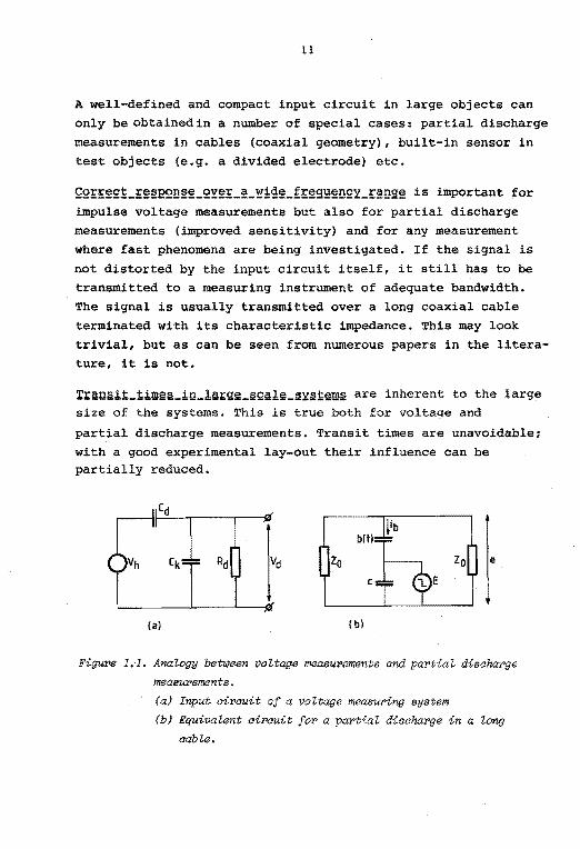
:l:à!Ul!i!iLUmê1o1_1n_J.ä;i;:gsi_!i!gäl!i_§:i.;.1.ït!ifü!lii! are inherent to the l.arge size of the systems. This is true both for voltage and
partial discharge measurements. Transit times are unavoidable;
with a good experimental lay-out their influence can be partially reduced.
Zo e
lal lb)
Figupe 1.1. Anal.ogy between vo'ltage measlU'ements a:nd partial disaharge
measurements.
(a) Input airauit of a voltage measuring system
(b) Equivalent airauit for a partial disaharge in a Zong
cab Ze.
12
An example of the similarity of voltage measurements and partial
discharge measurements can be found by comparison of two figures in this thesis. The left part of Figure 2 in section 2.2 (reproduced as Figure l.la) shows the differentiating part of
the voltage measuring system while the almost identical Figure 4.2 (reproduced as Figure l.lb) shows an equivalent circuit for
a partial discharge in a long high-voltage cable. Although the objectives are quite different, the equivalent circuits give a
clear picture of the similarity in the approach of the measuring systems.
1.3. Experimental facilities
All experiments described in this thesis were carried out in
the high-voltage laboratory of the Eindhoven University of Technology. The main dimensions of the shielded experimental enclosure are 24 x 18 x 14 m3• The damping of radiated inter
ference is 80 dB. The measuring apparatus can, whenever neces
sary, be located in a small screen room (2 x 1.5 x 2 m3).
The ac experiments were carried out with a Hipotronics resonant test set. Only one of the three modules (300 kV, 2A each) was used. The clean waveform of the 50 Hz resonance gives a good
suppression of conducted interference; this is especially important for partial discharge measurements. Impulse voltages were supplied by 5 stages of a 12 stage Haefely impulse voltage generator (200 kV, 2.5 kJ per stage).
A part of the experimental work for this thesis is described in three papers that were already published elsewhere. Two papers are co-authored by P.C.T. van der Laan who has initiated and stimulated this research. J.A.G. Bekkers, the other coauthor of section 2.2 performed most of the experimental work
reported in this section as a partial fulfilment of the requirements for a M.Sc. degree in Electrical Engineering.

13
2. VOLTAGE DIVIDERS WITH CONSECUTIVE DIFFERENTIATION AND
INTEGRATION
2.1. In:troduction
The measurement of high voltages generally involves the use of a voltage divider to bring the high voltage into a range that can
be measured by a meter, oscilloscope or digitizer. Exceptions to this rule are the electrostatic voltmeter where the full voltage appears across the measuring capacitor and some optical voltage sensors, based on the Kerr- or Pockels effect. The resistive divider is frequently used for the measurement of
de voltages. The electrostatic voltmeter and the generating voltmeter are also employed here. Measuring transformers are widely
utilized for the measurement of ac voltages (e.g. in power distribution networksl. In closed gas insulated systems (CGIS) the
utilization of capacitive dividers is growing; these systems have a favorable geometry for a cylindrical high voltage capacitor. Impulse voltages (switching, lightning, EMP) are measured
with capacitive, resistive and 111ixed dividers .and with optical sensors.
Most dividers consist of two or more similar impedance elements
to achieve - at least to a first approximation - a frequency in
dependent dividing ratio. When the high voltage branch has a number of high voltage components, the parasitic impedances make it increasingly difficult to obtain a flat frequency response
curve.
In this chapter a different type of divider will be described. The high voltage branch is a single capacitor of low value to avoid the problems with the parasitic impedances: the low vol
tage branch is a small measuring resistor. This divider has a ratio proportional to the frequency, in other words it acts as
a differentiator. The low value measuring resistor can be formed by the characteristic impedance of a correctly terminated measuring cable: this cable can then be as long as the physical lay-out of th.e testing area requires, without any effect on the
14
dividing ratio. To restore the shape of the original signal an integrator for the low voltage signal is necessary. Integration at the receiving end of a transmission line has the advantage that interf erence is also integrated, which means that an improved signal to noise ratio results. In fact the differentiator could be considered as a pre-emphasis network, analogous to the networks
used in phonograph recording or FM-transmission.
The principle of consecutive differentiation and integration has been used in the past for fast pulse measurements in plasma physics experiments [Ke 64]. In the following three sections its use for de, ac and impulse voltages is described.

15
2.2. Capacitive measurement of high de voltages
Capacltlve measurement of high de voltages G.G. Wolzak. J. A.G. Bekkers, and P.C. T. van der Laan
EiitdJioven UflilNusily q/Teclttrolog, DeparlmenJ Il/ Electrical Engilleeri•g. High Voltage <Poup. P.O. BOJ< j/], S600 MB Elmlno- T1te Netlterlmufs
tRecelved 20 April 1981; 4l<lOCpted for pubticaûoo 3 July 19811
Tbis paper describes a new technique for the capacitive measurement or high de voltages, based on the principle of consecutive dift'erentiation and integration. A measuring electrode acts as the dift'erentiating high-voltage capacitor; the e1ectric flux to the measuring electrode can be intercepted by a movable shield. The signa] is integrated with a commerically available integrator. The method bas excellent accuracy and linearity, while the long-term stability is detennined by the drift of the integrator. Calibration is only necessary after a change in the high-voltage circuit. The system is sensitive to corona, but the onset of corona can easily be observed by the operator. The described principle can a1so be used to measure 60 Hz. and impull!e voltages.
PACS numbers: 84. 70. + p
INTRODUCTION
High voltages are usually measured with voltage dividers consisting of combinations of resistors, capacitors, and inductors. The high-voltage components of these dividers are large in size and therefore tend to have appreciable parasitic capacitances and inductances. When a number of high voltage components are used, the parasitic impedances make it increasingly diflicult to obtain a fiat frequency response curve.
These problems are largely avoided if the bighvoltage branch or the divider consists of one single capacitor. Such a capacitor which could have air, SF6,
or oil as its dielectric can be a rather pure capacitive impedance. The otber components of the divider are in the low-voltage brancb and can be of nonna! si.ze; because only low impedance values are needed in tbis branch, quite pure impedances are possible.
In the configuration of Fig. l the high-voltage capacitance, for instance, formed by a measuring electrode at some . distance from a high-voltage object, carries a current
. d (CV) . dt/I 1=- h or 1=-, dt dt
(l)
where 'I' is tbe electrical flux ending on the measuring electrode. Equation ( 1) shows that integration is required to obtain a voltage proportional to V.; two methods are: (a) Z is a low-voltage capacitor. The divider is now a simple capacitive divider. The measuring instrument across the low-voltage capacitor should have a high impedance; (b) Z is a resistor. The RC combination differentiates, which means that a separate integrator is required. This principle, which was earlier employed by Keiler•·• for fast pulse measurements, is used in this paper for measurements of de voltages.
1. DIVIDER CIRCUIT
A circuit diagram of the measuring system is given in Fig. 2. The high-voltage capacitor is represented by
Cd; in addition a capacitance C • of the measuring electrode or the connecting cable to ground is shown. An operational ampliller with open-loop gain Ais connected as an integrator. The following equations can be derived:
(2)
(3)
and are valid for the frequency range
----- <t"' < R• + R, (4) A(R• + R,)C, R•RÁC• + C.)
At low frequencies the integrator starts to fall off; at very high frequencies Eq. (2) fails because the parallel impedance of C • and C • is no longer large compared to the parallel resistance of R • and R,. Note that C k has no influence on Eq. (2) when w satisfies the inequality Eq. (4). Two limiting ca8es of the general Eq. (3) can be considered: (i) R• < R,. Eq. (3) now tums into
Vo = R•C• v •. R,C,
(5)
In this case the dift'erentiating part of the system acts as a voltage source for the integrator. An advantage is ûiat R • can be ûie matching resistor at the end of a long signa! cable, so that the divider can have a flat response over a wide frequency range.• A disadvantage may be that the attenuation of the divider [Eq. (5)J can be too high.
(ü) R. i$> R 1• Equation (3) now changes to
c. v.=c,v •. (6)
where the assumption bas been made thatAC, > c •. Here R• can also be lert out. Clearly the voltage v.
and the capacitor C • act together as a current source for the integrator. In fäct this case can also be described
1572 Rev. Scl. lnstnmi. 52(10), Oct. 11181 0034-ll748181/10157243$00.60 C 1981 American IMlllule of Pllplca
(al
(b)
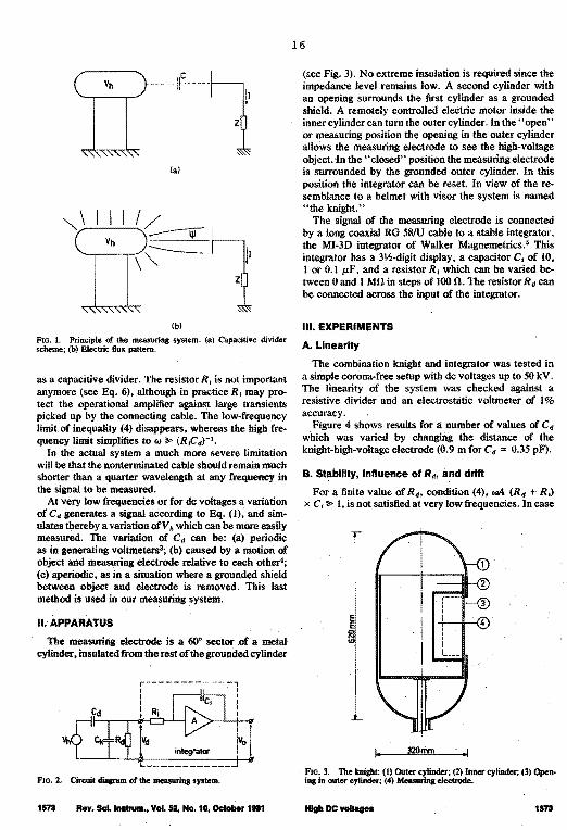
FIG. 1. Principle of the measuring system. (a) Capacitive divider seheme; (b) Electric flux pattem.
as a capacitive divider. The resistor R, is not important anymore (see Eq. 6), although in practice R, may proleet the QPerational amplifier against large transients picked up by the connecting cable. The low-frequency limit of inequality ( 4) disappears, whereas the high frequency limit simplifies to u; > (R,Cd)-•.
In the actual system a much more severe limitation will be that the nonterminated cable should remain much shorter than a quarter wavelength at any frequeney in the signa! to be measured.
At very low frequencies or for de voltages a variation of c. generales a signa! according to Eq. (1), and sim· ulates thereby a variation ofV h which can be more easily measured. The variation of c. can be: (a) periodic as in generating voltmeters3; (b) caused by a motion of object and measuring electrode relative to each other; (c) aperiodic, as in a situation where a grounded shield between object and electrode is removed. This Jast method is used in our measuring system.
11.APPARATUS
The measuring electrode is a 60° sector of a metal cylioder, insulated from the rest of the grounded cyliruler
-, 1 1 1 1 1
H 1
L------------.J F10. 2. Circuit diqram of the measuring system.
1573 Rev. ScL IHlrum., Vol. 52, No. 10, October 1981
16
(see Fig. 3). No extreme insulation is required since the impedance level remains low. A second cylinder with an QPening surrounds the first cylinder as a grounded shield. A remotely controlled eleetric motor inside the inner cylinder can turn the outer cylinder. In the "open" or measuring position the opening in the outer cylinder allows the measuring electrode to see the high-voltage object. in the "closed" position the measuring electrode is surrounded by the grounded outer cylinder. In this position the integrator can be reset. In view of the resemblance to a helmet with visor the system is named "the knigbt. H
The signa! of the measuring electrode is connected by a long coaxial RG 58/U cable to a stable integrator, the MI-30 integrator of Walker Magnemetrics. • Tuis integrator bas a 3Y.>-digit display, a capacitor C, of 10, l or 0.1 µ,F, and a resistor R, which can be varied between 0 and 1 MO in steps of 100 0. The resistor Rd can be connected across the input of the integrator.
111. EXPERIMENT$
A. Llnearity
The combination knigbt and integrator was tested in a simple corona-free setup with de voltages up to 50 kV. The linearity of the system was checked against a resistive divider and an electrostatic voltmeter of l % accuracy.
Figure 4 shows results fora number of values of c. which was varied by changiilg the distance of the knigbt-high-voltage electrode (0.9 m for c. = 0.35 pF).
B. Stablllty, influence of R., and drift
For a finite value of Rd, condition (4), ruA (R• + RJ x C, > 1, is not satisfied at very lowfrequencies. In case
32Qmm
FIG. 3. The knight: (1) Outer cylinder; (2) Inner cylinder; (3) Open-ing in outer cylincler; {4) Measuring electrode. .
1573
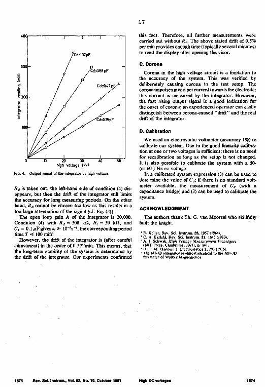
300
20 JO 40 50 high voltage (kV)
Fm. 4. Output sigoal of the integrator vs hiab voltage.
R 4 is taken out, the left-hand side of condition (4) disappears, but then the drift of the integrator still limits the accuracy for long measuring periods. On the other hand, R 4 cannot be chosen too low as this results in a too large attenuation of the signal [cf. Eq. (2)].
The open loop gain A of the integrator is 20,000. Condition (4} with R 4 = 500 kn, R1 50 kfi, and C1 = 0.1µ.Fgivesw > 10-•s-1,thecorrespondingperiod time T <Il 100 min!
However, the drift of the integrator is (after careful a(ljustment) in the order of 0.5%/min. This means, that the long-term stability of the system is determined by the drift of the integrator. Our experiments confirmed
1174 Rev. Sol. lnstrum.., Vol. 52, No. 10, October 1981
17
this fact. Therefore, all further measurements were carried out without Rd. The above stated drift of 0.5% per min provides enough time (typically several minutes) to read the display aft er opening the visor.
C. Corona
Corona in the high voltage circuit is a limitation to the accuracy of the system. This was verified by deliberately causing corona in the test setup. The corona impulses give a net current towards the electrode; this current is measured by the integrator. However, the fast rising output signa! is a good indication for the onset of corona; an experienced operator can easily distinguish between corona-caused "drift" and the real drift of the integrator.
D. CalibraHon
We used an electrostatic voltmeter (accuracy 1%) to calibrate our system. Due to the good linearity calibration at one or two .voltages is suflicient; there is no need for recalibration as long as the setup is not changed. It is also possible to calibrate the system with a 50-(or 60-) Hz ac voltage.
In a calibrated system expression (3) can be used to determine the value of Cd; if !here is no standard voltmeter available, the measurement of Cd (with a capacitance bridge) and (3) can be used to calibrate the system.
ACKNOWLEDGMENT
The authors thank Th. G. van Moorsel who skillfully built the knight. '
1 R. Keiler, Rev. Sci. lnstrum. 35, 1057 (1964). 'C. A. Ekdahl. Rev. Sci. lnstrum. SI, 1645 (1980). 3 A. J. Schwab, Hl Measuremem Techniques
(MIT Press, 141. 'H. T. M. Haenen, J. , 203 (1976). 'The Ml-3D integrator is almost ideotical to the MF-3D
fluxmeter of Walker Magnemetics.
High DC voftllgn 1174

18
2.3. The measurement of ac (50 Hz) voltages with a differ
entiating/integrating divider
voltage measureroents in high voltage networks are important for protection and for monitoring the energy flow. Up till several
years ago voltage measuring in networks was exclusively done with inductive voltage transformers. The increasing number of
CGIS-stations and the modern protective circuitry have changed
this fact. In CGIS capacitive dividers can be used advantageously because the necessary high voltage capacitors can easily be built into
the system. Secondly the power, required by the modern protec
tive equipment has been reduced by two orders of magnitude [To 82], which makes the capacitive divider with its smaller power output more acceptable.
The possibilities for utilizing the differentiating/integrating
divider as voltage monitor in substations are discussed in this section. The theory of the system is identical to the theory described in the sections 2.2 and 2.4. The special requirements concern the measurement of 50 Hz voltages with a low amplitude error (up to 0.1%) and. a low phase error (down to 5'), which
are necessary for the varfous categories of measuring systems in power engineering.
The accuracy is determined mainly by the high voltage capacitor. Small variations as a function of temperature or pressure (for
a compressed gas capacitor) can lead to unacceptable errors. This is a matter of proper design of the hv capacitor1 further
details can be found in the literature {Gr 69] and will not be treated here.
The phase error requires a special design of the integrator. Generally an active integrator is used but as was shown in section 2.2 the drift in the output signal of an active inte
grator is a problem. For measurements in substations drift is, of course, unacceptable. This means that the werking point of the integrator has to be stabilized for de by means of an additional resistor R2 , see Figure 2.1. The output voltage V
0

19
differentiatlng part-1- d c stabilized integrator 1
Figure 2.1 : Ac vol:tage divider> '!Vith de stabiUzed integrator.
is then given by:
(2 .1)
if the open loop gain A is high. The phase difference $ between
V0
and Vd can be calculated from (2.1):
(2. 2)
For an ideal integrator $ equals -~/2; the phase error of the integrator from Figure 2.1 is therefore:
(2. 3)
A phase error 8$ smaller than 5 1 at a frequency of 50 Hz is
obtained for values of R2Ci larger than 2.2 s. The phase error in the differentiating part is negligible; the differentiation of course introduces a phase shift of ~12.
Capacitive voltage monitors in CGIS can lead to a peculiar
measuring problem, usually referred to as the "trapped charges problem" {IE 79]. If the circuit breakers of a transmission line open, some charge can be left on the line (and the divider).

20
If on subsequent reclosure these charges have not entirely decayed, while the output of the integrator has gone to zero (with a time constant R2Ci} a de error appears on the output, superimposed on the ac voltage. This error dies out with
the same time constant R2ci, which is unacceptable for accurate measurements. It must be stressed however, that this phenomenon is inherent to all measuring systems which fail to correctly measure de voltages. Inductive voltage transformers fail also
in this respect hut provide a de path for the charges to leak away. If by some other means a de leakage path is provided - as
is anyway desirable to avoid dangerous overvoltages on CGIS -the capacitive voltage monitor will also function correctly.
FigUPe 2.2 : Mixed passive/active integr>ato~ !üith imp!'OVed pulse ~sponse.
If a measuring system is to be used to actuate protective circuitry, it must be.able to give an accurate reproduction of transient signals. The rapidly changing high voltage causes a lar~e current through the high voltage capacitor Cd in Figure 2.1. Apart of this current goes through R1 and therefore the operational amplifier must be able to supply as large a feed
back current through c1 • This requires a carefully selected operational amplifier. In a modified integrator design, in which the passiva integrator preceeds the active one the requirements on the operational amplifier are less stringent. Figure 2.2 gives an example of such a design. The choice of the components is governed by the condition:

21
(2.4)
Some successful laboratory experiments at 50 Hz voltages were carried out with the coaxial high voltage capacitor ESPOM, des
cribed in the next section. Basically the measuring principle seems quite suitable for voltage monitors in substations.
Extensive field tests and further work on the accuracy is however needed to convince potential users. Field tests will be
carried out in the near future.
2.4. A new concept for impulse voltage dividers
FOURTH INTERNATIONAL SYMPOSIUM ON HIGH VOLTAGE ENGINEERING
61.11
ATHENS • GREECE, 5 • 9 SEPTEMBER 1983
A NEW CONCEPT FOR J:MPULSE VOLTAGE DIVIDBRS.
G.G. Wolzak and P.C.T. van der Laan
Eindhoven Uni ver si ty of Technoloqy Department of Electrical Engineering Eindhoven, The Netherlands.
~ In this paper we propose a new concept for impulse voltage di.viders based on the principle of consecutive differentiation and integration of the eignal. The high Voltage element is a single qas-filled capacitor. This capacitor toqether with a long, characteristically terminated measurinq cable which acts as a low valu-e resistor, forms the differentiating part of the system. Integration is carried out by e:l.ther a passive or an active integrator. we report measurements on standard {~"2/50 JJS) pulses in addition the response if the divider is measured according the "sphere-gap'" method. These measurements show the good transient behavior of the system. We dis.cus.s the most ·adequate type of integrator to be -used and we pay attention to the shielding precautions, associat-ed with the use of a '"nonnal" oscilloscope for impulse voltage measurements.
Keyworàs
capacitor, divider, measuremenL
1. Introdt.lction: capacitive divider problems.
:ro:c the measurement of hiqh impulse voltage$, a _ voltage divider has to reduce the high voltage of up to some MV to a value that can be measured by an oscilloscopa. For modern oscilloscopes this valua is about 10-SO V. The low voltage signal must be a good. reproduction of the rapidly changing high voltage. 'l'hree types of divider can be distinguished; resistive, capacitive and mixed dividers~ Resistive divide.rs with a low value of the total resistan~e (e.g. to km tend to load the high voltage circuit severely; high ohmic dividers suffer- from the influence of stray Capacitances. Mixed dividers; having resistors and capacitors either in series or in parallel are used in many la:boratories but tend to be rather complex and pose a linearity problem. The advantages of a single capacitance in the_ high voltage circuit have been described pr~viously. This capaci tance can be a compre:ssed gas capacitor [ 1] or be formed <by an electrode at some distance of a high voltage object [2]. Also the use of a coaxial tubular capaçitor for testing metal enclosed switchgear has been reported [3]. · The problemsr associated with the use of undamped capacitive 9,ividers can be $tnnmarized as follows; a) Natural frequencies of the low voltage arm.
Specia.l care has to be taken to,ensure a very low inductance of the low voltage arm. usu~lly special capa_ci tors [ 4) or a numbe:r of capacitors in parëlllel [5] are emloyed.
b) Travelling wave oscillations on the transmission line between the hiqh- and the low-voltage arm. These oscillations occur when a compressed gas capacitor is used_ I 1] •
ei The matching of signal cable which can.not be properly with it:S characteristic impedance. To pi:event multiple reflections, a series resistor is often employed,
22
2 . The new approach~
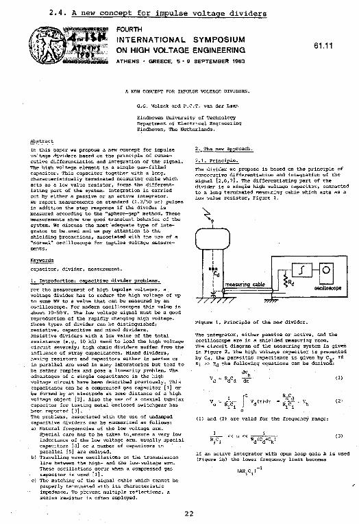
2 .1. Principle.
The di vider we propose is based on the principle of consecutive differentiation and inte9ration of the
[2,6, 7]. The differentiatin9 part of the is a single high voltage capacitor, connected
to a long te.rminated measuring cable which acts as a low value resistor, Figure L
Fiqure 1. Principle of the new divider.
'l'he integrator, either or active, and the oscilloscope are in a measurinç room. Tbq circuit diagram of the measuring system is giveD in Figure 2. The high voltage capacitor is presented by Cfü the parasitic capac-itance· is given by ck. If Ri » Ra the followiug equations can be derivcd:
(1)
(2)
( 1) and (2) are val id for the frequencY range:
(3)
lf an active integrator with open loop 9ain A is used (Fi9ure 2l;i) the lower frequency limit becomes
(ARiCi)-1
.--------ï
<al
<bl
Figure 2. Equivalent circuit of the measuring system a. with passive integrator b. with active integrator
Equation (2) gives the ratio of the divider. The
~~o:c~=~~~s dete~~~e!,~ c::o!e:~~!e!11~:lse small (R1c1 = - 10-3 s}. Ra is generally 50 ohm and Cd is 10 100 pF. This tneans that the divider ratio (the attenuation of the signal) wil! be in the order of 105 to 10 7.
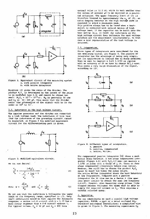
2. 2. lnductance in the high voltage circuit.
The impulse generator and the divider are connected by a high voltage lead. The inductance of this lead {iind the inductance of the 9roundin9 circuit) cannót be neglected. In Fiqure 3 the modified equivalent circuit for the differentiating part is 9iven.
L
Figure 3. Modified equivalent circuit.
we can now der i ve:
With Q = and
+ 1
2 w =
0
(4)
(5)
We can see that the inductance L influences the upper limit of the -frequency range, specified in (3). very smal 1 inductances would in fact improve the frequency response; a series L-C-R circuit with ~ 12 ha.s a more linear response than a C-R without :r... Fo.r t.ypical values, Cd = 10 pF and Rd = SOQ this
23
optimal value is 12.S rtH1 which is much smaller than the values of several µH to be expected in a practical situation. The upper frequency limit of (3) is therefore lowered to approximately the w of (5). An extra darnpin9 resistor at the high volta~e sid~ is required to avoid a resonance peak. This problem always has to be faced when a testobject is connected with sev-eral meters of high voltage lead~ !f the can be built into the test set-up (e.9. in high voltage circuit does influence the test voltage waveform and the measurement simultaneously. In that case a true representation of the test voltage is obtained.
2. 3. Integrat ion.
Th.ree types of integrators ware considered for the new measurin9 sée Figure 4. The passive RC in1;;egra,,or has advantage of being ve.ry simp!e, but application is limi ted due to droop problem$. When we want to measure a full L 2/50 us imp•1lse wi th an accuracy of 5% we have to choo~ RC > 2 msec. This means a very large attenuation of the Signa!, according to (2}.
%1 ~ c1 Jvo 11-~~~~-'--~~~ ....... ~4
Figure 4. Different types of integrators. a, passive b. passive, compensated c. active, Miller"
(al
(b)
(C)
The compensated passive integrator [ 8] shows a much better drOop behavior. A two compensated inte-grator 4.b) with R1Ci = msec can measure a 1.2/50 µs vith a droop of < 1i. Three or four stage compensated integrators behave even better. However, one still has to choose the product RiCi equal to about ten times the pulse length. The active Miller integrator shows ·the best behaviour at low frequencies. Cropared with a passive inteçrator the RC time can be a factor A (the open loop 9ain} smaller to obtain the sa.me low freque."lcy cut-off. aowever, when rn.easuring steep pulses (like chopped impulsé' voltages) the opamp must be able to supply the required current in Ci. This requires a careful ~elected opamp~
3. Apparatus.
ti'or our e.xperiments we used a coaxial high voltaqe capacitor, ESPOM, a part of a metal enclosed SF6-insulated switchgear 1nstallation; a simplified view is given in Figure 5~ The measuring capacitance Ca
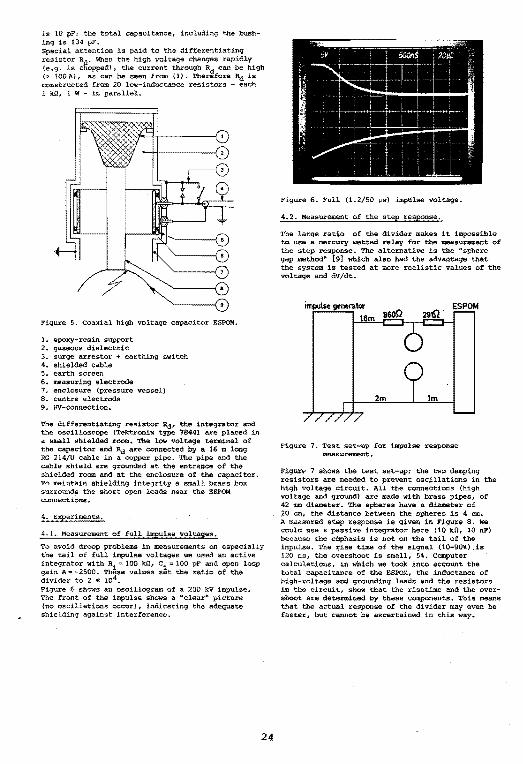
is 10 the total capaci.tance, including the bush-inq is pF. Special attention is pa.id to the differentiating resistor When the high voltage changes rapidly
is 1 the current through Rd can be hi9h {> A.}, as can be seen from (1}. '!'herefore Rd is constructed from 20 low-inductance resistors - each 1 kQ, 1 W in parallel.
Figure 5. Coaxial high voltage capacitor ESPOM.
1. epoxy-resin support 2. 9aseous dielectric 3. surge arrestor + earthing switch 4. shielded cable 5. earth screen 6. measurin9 electrode 7. enclosure (pressure vessel) 8. centre elect.rode 9. HV-connection.
The differentiatinq resistor the oscilloscope (Tektronix a small shielded room" The low the capacitor and Ra are connected a 16 m RG 214/U cable in a copper pipe. The pipe and cahle shiel.d are grounded at the ent.rance of the shielded room and at the enclosure of the capacitor. To rnaintain shielding inte9rity a small brass box surrounds the short open leads near the ESPOM connections •
4.1. Measurement of full impulse voltages"
To avoid droop problems in measurements on es1oec:1a11v the tail of full impulse voltages we used an integrator with R1 ""' 100 k.0 1 ei= 100 pF and open loop gain A = -2500. These values set the ratio of the divider to 2 K 104 ~ Figure 6 shows an oscillogram of a 200 kV The front of the impulse shows a "clear" {no oscillations occur), indicatinq the shielding against interference.
24
Figure 6. Full {1.2/50 µs) imptilse voltage.
4.2. Measurement of the step response.
The large ratio of the divider makes it impossible to use a mercury wetted reLiy for the measurement of the step response" The alternative is the "sphere gap method'' (91 which also had the advantage that t:he system is tested at more real.istic values of the voltage and dV/dt"
Împulse generator
t6m
Figure 7. Test set-up for impulse response measurement.
Fiqure 7 shows the test set-up; the two damping resistors are need.ed to prevent oscillations in the
voltage circuit~ All the connections (high and are made wi th brass pipes, of
The spheres have a diameter of ,;!O cm 1 the distance between the spheres is 4 cm. A measured step response is gi ven in F.tqu::e 8. We could use a integrator here (10 k!l, 10 nF)
is not on the tai l of th'il time of the signal {10-90%). is
the overshoot is small, 5%. Computer ca1e>>1at1<ms. in which we took into account the
of the ESl?OM. the inductance of hi•,h··volt<><•• and grounàing leads and the resistors
cir<:uit, show that the risetime and the overshoot are determined by these components. This means that the actual response of the di vider may even be faster, but cannot 'be ascertained in this way"
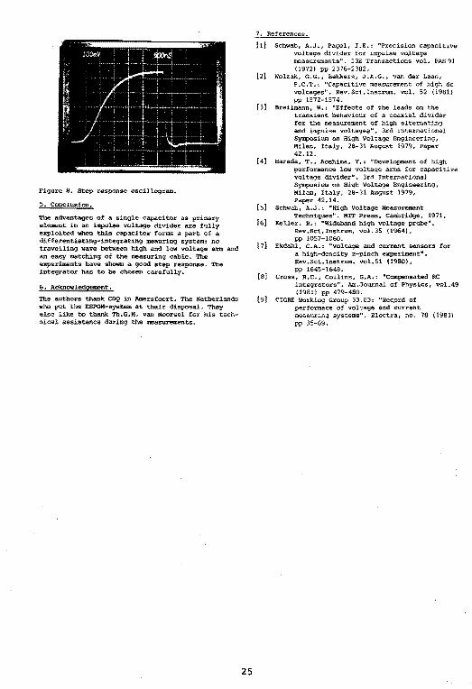
Fiqure a. Step response oscillogram.
s. ConcJ.usion.
The advantages of a as primary element in an impulse are fully exploited when this capacitor forms a part of a differentiati.n9-inteqratinq maurinq systènu no travell.ing: wave between high and low voltage arm and an easy matching of the cable. The experiments have shown a qood integrator has to be chosen r~~•'nllv
6. Acknowledgement.
The authors thank COQ in All>er•1foor10, whO pUt the BSPOM-system at t.heir also like to thank Tb.G.M" van nical assist.ance durinq the me:asurements~
25
7. References.
{1] Schwab, A.J., Pagel, J.E~: uPrecision capacitive voltage divider for impulse voltage measurements". l3E Transactions vol. PAS 91 (1972) pp 2376-2382.
[2) Wolz.ak, G.G., &akkers, J.A.G., van der Laan, P.C.T.: °Capacitive measurement of hi9h de voltages". Rev .Sci. Instrum. vol. S2 0981} VP 1572-1574.
[3] Breilmann, w.: "t:;ffects of the leads on t.he transient behaviour of a coaxial di vider for the measurement of high and impulse voltages". 3rd Int.er11atio11al Symposium on High Voltage Engineering, l4ilan 1 ltaly. 28-31 August 1979, Paper a.u. ·
(4] Harada, T., Aoshima, Y.: "Development of high performance low voltage arms for capacitive voltage divider•. 3rd International Symposium on Hiqh Volt.él9e En9ineerin9, Milan" Italy, 28-31 August 1979, Paper 42.14.
[s] Schwab, A.J.: "High Voltage Measurement Techniques" • MIT Press, Cambri&)e 1 19 71 •
[6] Keller~ R.: "Wideband high voltage probe"". Rev.ScLinstrum. vol. 35 {1964), pp 1057-1060.
[7] Ekdahl, C~A~: "Voltage and current sensors for a high-density z-pinch experiment". Rev.ScLinstrum. voLSl (1980) / pp 1645-1648.
[8] Cross, R.C., Col.lins, G.A": 11 Compensated RC integrators". Am.Jou.rnal of Physics, vol.49 (1981) pp 479-480.
[9] CIGRE Working Group 33.03: "Recprd of performace of voltage and current mea$urin9 systems". Electra, no. 78 (1981) pp 35-69.
26
3. A GENERATING VOLTMETER WITH PIEZO ELECTRIC MODULATION
3.1. Introduction
Generating voltmeters were originally developed as non-contacting de voltmeters or fieldmeters. Their common aspect is a mechanically modulated measuring electrode, capacitively coupled to the
test object (or test field). The modulation generates an ac signal, proportional to the voltage difference between electrode
the high voltage object. Three basic modulation techniques can be distinguished Ivo 74]: - the rotating segmented disc (field mill},
- the oscillating vane (tuning fork), - the vibrating capacitor. All three principles have been developed into commercially available instruments. The vibrating capacitor technique was first described by Zisman fZi 32], who used a piano wire to
drive an electrode. Later versions of Gohlke and Neubert [Go 40] and van Nie and Zaalberg [Ni 63] use a coil and a membrane capacitor respectively.
In this chapter the possibilities of a vibrating capacitor driven by a piezo electric crystal.will be examined. The use of a piezo
transducer has two advantages: - the vibration frequency can be significantly higher than the
frequency obtained with other transducers. This opens the possibility to widen the frequency range of the high voltage to be measured. Whereas for instance the field mill can only be used to measure de voltages, an extension to at least power frequencies (50 or 60 Hz) is very interesting.
- The reliability of a transducer is much higher than that of
the other techniques, because mechanical wear is no longer important.
A possible problem is the small amplitude of the vibration (a few µm), which will lead to very small signals.
27
3.2. Theory
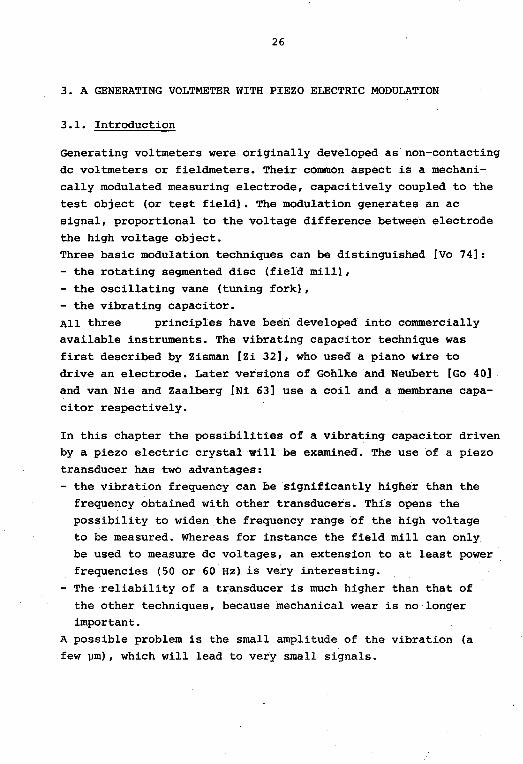
Consider the capacitor of Figure 3.1. The distance between the high voltage electrode and the central low voltage (measuring) electrode varies as. a function of time according to:
(3.1)
hv electrode .................... -;......,. ............... ,
d(t)
\~guard !I moving electrode
Fi(Jm'e 3 .1 : rnn!.?ip Ze of vibroting p late aapaoi to1'.
If the measuring electrode has an area A and (3.1) is substituted in the expression for a parallel plate capacitor, the capacitance C(t) is given by:
(3 .2)
The displacement current I flowing from the measuring electrode to ground can then be calculated:
I (t) (3.3)
Two cases can be distinguished:
28
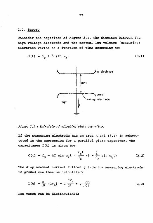
A. The voltage Vh is a de voltage: dVi/dt = O. Eq. (3.3) turns into a very simple expression:
dC I(t) = Vh dt
Combination of (3.4) with (3.21 gives:
C0
was already def ined as
(3. 4)
(3. 5)
(3 .6)
The current I is a sinewave with an amplitude proportional to
the high voltage Vh' see Figure 3.2.
-t
{al ( bl
FigU'l'e 3,2 : The input voltage (a) and the output current (b) for> a high
da voltage.
B. The voltage Vh is an ac voltage:
(3. 7)
where wh << wk.
The current I bas two components, according to (3.3):

29
(3 .8)
(3. 9)
I
1 -t
lal (bi
Figul>e 3.3 The input voltage (a) and the output au:tTent (bJ fo1' a high
ao vo"ttage.
The first component I 1 represents the normar displacement current and is independent of the movement of the electrode. The current r 2 is a modulated ac current, see Fiqure 3.3. The type of modulation is known as double sideband suppres.sed carrier (DSSC) modulation [Ca 75]. The frequency spectrum of
I 1 and r 2 is given in Figure 3.4.
I2
I1
l ,..._..,__,
l 1
Wh Wk-Wh Wk Wk+Wh
Figu.re 3.4 : F1'equenay speat1'U11'1 of the output aU1'1'ent (I1 + I 2J fo1' a
high ac voltage.
The currents, described by (3.5} and (3.9) have to be measured and demodulated to obtain a signal proportional to the voltage
30
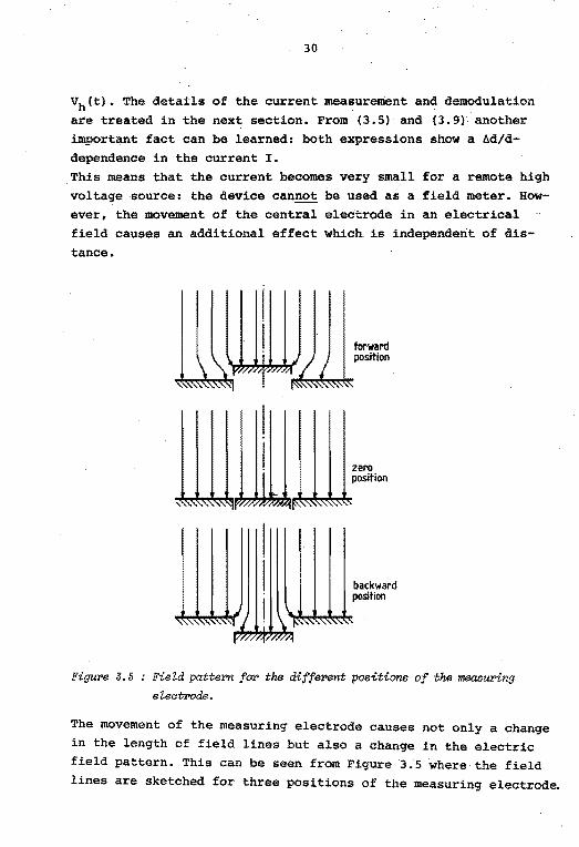
Vh(t). The details of the current measurement and demodulation are treated in the next section. From (3.5) and (3.9} another important fact can be learned: both expressions show a àd/ddependence in the current I. This means that the current becomes very small for a remote high voltage source: the device cannot be used as a field meter. However, the movement of the centra! electrode in an electrical field causes an additional effect which is independent of distance.
1
i ~ ' ' "
forward position
zero position
backward position
Figure 3.5 FieZd pattern for the diffe:r>6nt positione of the measuring eZ.eatrode.
The movement of the measuring electrode causes not only a change in the length of field lines but also a change in the electric field pattern. This can be seen from Figure 3.5 where'the field lines are sketched for three positions of the measuring electrode.

31
The variation in the number of field lines is equivalent to a time varying flux, in other words to a small curren~
An exact calculation of the amplitude A~ of this flux-change requires a detailed knowledge of the electric f ieldstrength
along the electrode. This problem can be solved by conformal
mapping for a two dimensional situation [Be 63] but this solu
tion gives a diverging value for ~~ at large distances from the
high-voltage electrode. For an electrode in the form of a half
sphere, the flux to the half sphere is 3~r2 e0E0 [Pr 69], where
r is the radius of the sphere. Compared to the flux to the plane,
when the half sphere has flattened out this corresponds to ~~
2ffr2
eOEO. For a vibrating circular electrode of radius r in a plane a first order approximation is adopted here.
Figur>e 5.6 : Ea:tension of the field distUPba:nae in the ea:tr>eme position of the eZeatrode.
If the field pattern of Figure 3.6 is assumed for the forward position of the measuring electrode then additional flux coming
from a radius r + Ar is seen to end on it. The additional flux
is limited by the field line whichendsin the lower corner. Since this field line leaves under 45° it is reasonable to
assume that Ar = a. The extra flux A~ is then:

32
(3.10)
In the extreme downward position the total flux to the measuring
electrode is diminished by áw. If the movement of the electrode is given by (3.1), the current
generated by this variation in the flux is:
(3.11)
This expression is similar to (3.5): a time independent field E
0 is assumed. For a time dependent field expressions comparable
to (3.8) and (3.9) are obtained. The next question is: what is the relative importance of these two effects? The ratio of I/I3 can be calculated from (3.5) and (3.11):
(3.12)
The . currents are equal for r
I 3 component is dominant.
2d0 ~ for larger distances the
3.3. Apparatus
In this section the different components of the generating voltmeter system will be treated. The realization of the vibrating electrode will be described first. Then attention is paid to the current measuring system, consisting of a Rogowski coil and a loek-in amplifier, which also acts as a demodulator for the signals.
The design of the test set up with a vibrating measuring electrode is based upon two important considerations:
- efficient coupling between the piezo-electric crystal and the electrode,
- the exciter signal of the crystal must remain decoupled from the current to be measured.

33
The approach to fulfill these requirements is sketched in
Figure 3.7.
transducet
/ / / , ..... ....,....,....,....,....,...,,...,...,....,.....,./
Figure 3.7 : The test set-up !Ji.th the Sonair transducer.
The vibrating front plane of a commercially available transducer (Sonair 2 from Vernitron Ltd) serves as a measuring electrode. The aluminum housing of the transducer gives a good shielding against the excitation signal of the crystal. Figure 3.7 also illustrates why the measurement of the displacement current requires special care: a small current is superimposed on the much larger excitation current of the transducer. The use of a Rogowski coil is ideal here: the current for the transducer is f ed through a coaxial cable and the measuring

34
current goes through the sheath of the cable. The Rogowski coil only "sees" the net current. Further details of the coil will be
given later in this section. The transducer (28 mm diameter} is placed in the center of an alurninum Rogowski-profiled electrode (15 cm diameter} • The high voltage electrode is identical in shape. The system operates at
a frequency of 40 kHz, the estimated amplitude of the vibration is in the order of .1 µm.
windlngs n=100
Figure 3.8 Prinaivie of the ROÇ101VSki aoiZ.
The simplest way of current detection. is usually the measurement of the voltage dr0 p over a series resistor. However, a series resistor cannot be used with the Vernitron transducer while application with the HPA transducer is somewhat difficult. Furthermore a resistor implies galvanic coupling between the
sensitive measuring circuitry and the high voltage circuit~ this can be disastrous in the case of a breakdown or flashover. A Rogowski coil offers a good solution but the transfer impedance, defined as the ratio of output voltage and input current must be as high as possible. Figure 3.8 gives a picture of the coil and Figure 3.9 a simple equivalent circuit. The mutual inductance can be calculated with:
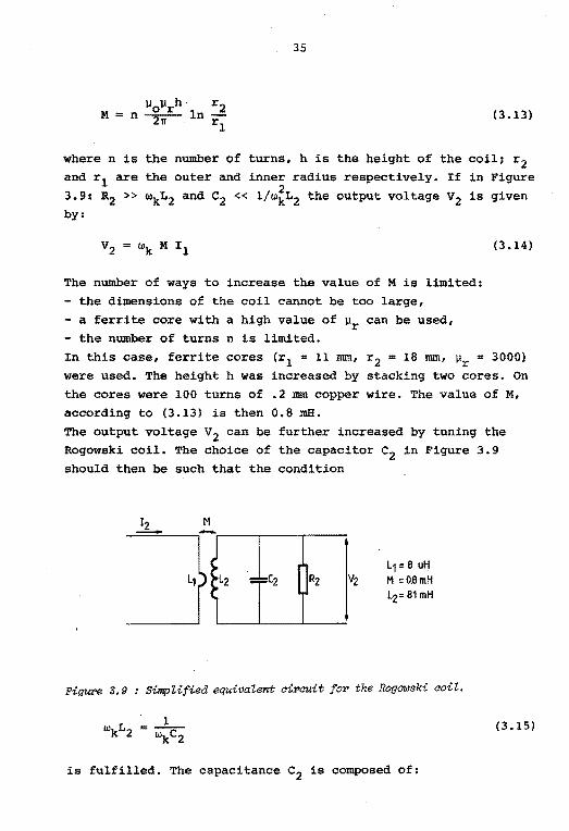
35
where n is the number of turns, h is the height of the coil1 r 2 and r 1 are the outer and inner radius respectively. If in Figure
3.9: R2 >> wkL2 and c2 << 1/w~L2 the output voltage v2 is given by:
The number of ways to increase the value of M is limited: - the dimensions of the coil cannot be too large,
- a ferrite care with a high value of µr can be used,
- the number of turns n is limited.
(3.14)
In this case, ferrite cores Cr1 = 11 mm, r 2 = 18 mm, µr = 3000) were used. The height h was increased by stacking two cores. On
the cores were 100 turns of .2 mm copper wire. The value of M, according to (3.13) is then 0.8 IDH.
The output voltage v2 can be further increased by tuning the Rogowski coil. The choice of the capacitor c2 in Figure 3.9
should then be such that the condition
Lp8 uH M :O.BmH Lz= 81 mH
Figu;l'e 3.9 Simplified equivalent aircuit for the RogOliJski coil.
is fulfilled. The capacitance c2 is composed of:
(3 .15)
36
- the capacitance of the cable to the voltmeter, - the input capacitance of the voltmeter, - the tuning capacitance. The output voltage of the tuned Rogowski coil is given by:
(3.16)
where Q is the quality factor of the secondary circuit:
(3.17)
The value of R2 (the input resistance of the voltmeter) can be chosen high {e.g. 100 Mn) to inèrease Q. In practice, however, Q is limited by the losses in c2 , L2 etc. A practical value for
Q, also confirmed by a number of measurements is: Q = 30. It must be stressed that the tuned coil has a strong frequency selective behavior. This is normally considered as a disadvantage for a wideband measuring system but it is a big advantage for a
carrier besed system like this. From (3.17} a transfer impedance can be derived:
{3.18)
The value of Rt gives the apparent measuring resistance, seen from the voltmeter's side. For this situation a value for Rt of 6 kQ can be calculated. The high voltage circuit "sees" in the ground lead only an impedance of Q ook L1 (= 60 Q).
This section concludes with a basic description of the loek-in amplifier. A loek-in amplifier is an ac voltmeter, which is able to measure the amplitude of a signal of known frequency in the presence of high level background noise or interference. Basically a loek-in amplifier is a phase sensitive ac voltmeter
which compares an input signal with a reference to produce a de signal output whose level is proportional to that part of the signal synchronous and in phase with the reference.
37
AC. SIGNAL CHANNEL
: SIGNAL 1 OUTPUT
-------------1 (OC) r------------- -,
REFERENCE : PHASE - PHASE - 1
INPUT ---HLQCKEO SHIFTER 1
CAC) f 11 1
f~i3j QJ 1 ! '------- _______ J
REFERENCE CHANNEL
Figu:Pe 3.10 : BZock diat;ll'<lPl of the Zoek-in amplifier.
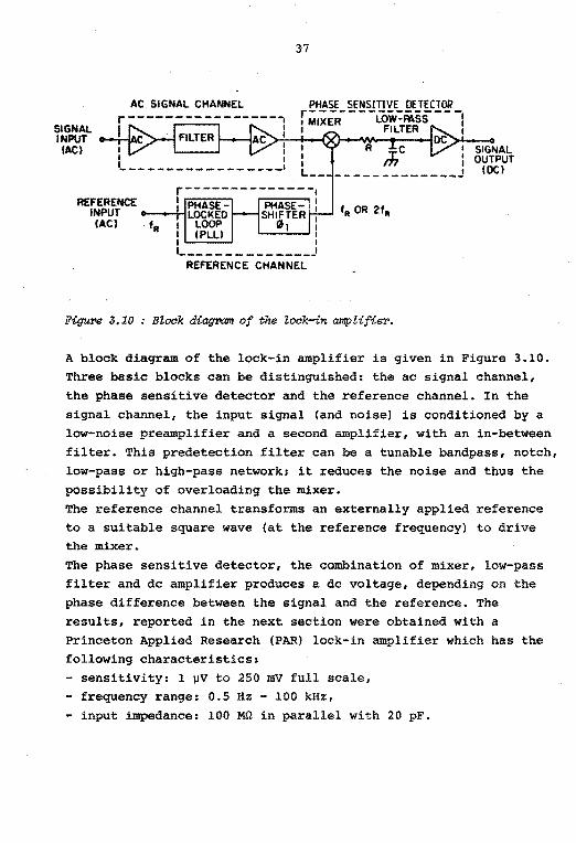
A block diagram of the loek-in amplifier is given in Figure 3.10. Three basic blocks can be distinguished: the ac signal channel, the phase sensitive detector and the reference channel. In the signal channel, the input signal (and noise) is conditioned by a low-noise preamplifier and a second amplifier, with an in-between filter. This predetection filter can be a tunable bandpass, notch, low-pass or high-pass network; it reduces the noise and thus the possibility of overloading the mixer. The reference channel transforms an externally applied reference to a suitable square wave (at the reference frequency) to drive the mixer. The phase sensitive detector, the combination of mixer, low-pass filter and de amplifier produces a de voltage, depending on the phase difference between the signal and the reference. The results, reported in the next section were obtained with a Princeton Applied Research (PAR) loek-in amplifier which has the following characteristics: - sensitivity: 1 µV to 250 mV full scale, - frequency range: 0.5 Hz - 100 kHz, - input impedance: 100 Ma in parallel with 20 pF.

38
3.4. :Experiments1 discussion
The system with the Sonair 2 transducer (see Figure 3.7) was
tested with de voltages up to 30 kV and 50 Hz ac voltages up to 20 kV rms. The output voltage of the loek-in amplifier was compared to a direct high voltage measurement with a Singer electro
static voltmeter (error 1%).
150 uv (ac)
f 100
50
0 0.5 1.0 1.5 2D -vh (kVHrms tor ac)
1.5 mV(dc)
î 1.0
05
Figure 3.11 Output vo"ltage of the 'loek-in ampUfier ve:vsus high-voltage.
Test set-up with the Sona.ir transducer.
Figure 3.11 gives a picture of the linearity of the system. The
distance between the electrodes was .l mm in these experiments. The linearity is very good, both for de and ac. The measured
signal is roughly a factor 10 smaller with ac voltages. This is caused by a low-pass filter in the loek-in amplifier (time
constant ·10 ms, 6 dB/octave) which gives a 10 dB damping for 50 Hz signals. This filter was built in the loek-in amplifier
and could not be switched off: for a 50 Hz measuring system a more appropriate filter would have to be constructed.
250
uV
-î 200
150
100
50
·50
39
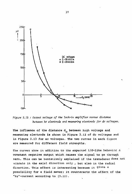
OC voltages o E=10kV/cm x E=20kV/cm
Figure 3.12 Output voitage of the Zoek-in amplifieP versus distance betüleen hv eiectrode and measuring e7.eC!trcde for> de voltages.
The influence of the distance d0
between high voltage and measuring electrode is shown in Figure 3.12 of de voltages and in Figure 3.13 for ac voltages. The two curves in each figure are measured for different field strengths.
The curves show in addition to the expected l/d-like behavior a constant negative output which causes the signal to go through zero. This can be tentatively explained if the transducer does not vibrate in the axial direction only , but also in the radial direction. This effect is interèsting because it gives a possibility for a field meteri it counteracts the effect of the "à~"-current according to (3.11).

20
10
5
·S
40
AC voltages a S kV/cm !RMSl , • 10kV/cm ( RMSl
Figure 3.13 Output voZtage of the Zoek-in anrplifier versus distanae
bet;ween hv eZeatrode and measuring eleatr'Ode for aa voltages.
These effects clearly cannot be separated with this transducer.
To inhibit the vibration in the radial direction a new test set
up has been designed, see Figure 3.14; also here a commercially available transducer (Philips HPA) has been used. This set-up has two advantages:
- the amplitude of the vibration is larger: 20 µm,
- the elongation of the moving part gives a movement in the
axial direction only.
The main disadvantage of the HPA is the low operating frequency, 5 kHz, which is in the audible range.
Due toa number of experimental.difficulties no extensive
measurements have been carried out up till now.
41
~t---t<c+~~tr~••~•d~u~ce~r
~
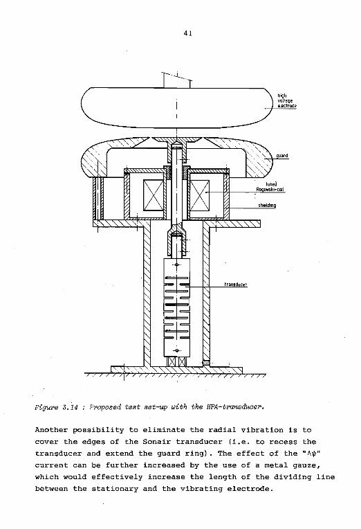
* Figure 3.14 : Proposed test set-up with the HPA-transduaer.
high voltage electrode
Another possibility to eliminate the radial vibration is to
cover the edges of the Sonair transducer (i.e. to recess the
transducer and extend the guard ring). The effect of the "llljl"
current can be further increased by the use of a metal gauze,
which would effectively increase the length of the dividing line
between the stationary and the vibrating electrode.
42
4. WIDE BAND DETECTION OF PARTIAL DISCHARGES IN HIGH VOLTAGE
CAB LES
4.1. Introduction
This chapter describes a method for wide band detection of
partial discharges in high voltage cables.
A partial discharge is defined as an electrical discharge which
bridges the insulation between conductors only partially. When
an insulating material is stressed electrically partial dis
charges may occur in gas filled cavities in the material,
cavities which cannot be completely avoided during the manu
facturing process. The partial discharges may give rise to a
progressive deterioration of the insulation and eventually to a
complete breakdown. The detection of partial discharges has
therefore become a routine procedure for acceptance testing of
power cables, switchgear, transformers etc.
In a partial discharge electrons and ions flow during a short
time (less than l µs} whereas simultaneously acoustic, optical
and radio frequent energy is emitted. An electrical measurement of the current flow caused by the discharge is a practical
measuring method for a power cable. A wide band measurement offers the following advantages:
- the detection sensitivity can be increased,
- in cables transit time measurements are possible which means
that a localization of the discharge site is feasible, - the actual shape of the pulse from the discharqe in the void
can be studied.
In this chapter first attention is paid to an equivalent circuit
for a partial discharge. Then the attenuation of the rf signals
in the cable is treated. In the following sections several
detection methods are discussed and the chapter ends with a
number of experimental results among which oscillograms of actual pd signals are shown.

43
4.2. Theory
The description of the electrical phenomena related to partial discharges is usually based on the equivalent circuit of Figure 4.1 [Kr 64]. Capacitorc isthe capacitance of the void, ais the capacitance of the sample and b is the capacitance of the dielectric between the electrodes and the void, in fact b con
sists of two capacitors in series. The spark gap symbolizes the
breakdown of the cavity.
:n
Figure 4.1 : Equivatent aircuit .fo~ a p~tiat disaht:r:r>ge.
This model does not. give ·!l representation of the actual physical mechanism of a partial discharge and cannot explain the differ
ent waveforms of the curre.nt pulses, reported in the literature [Kä 76, Lu 79]. Furthermore, the essential effects of transit times and the dissipation cannot be·described by the simple
equivalent circuit of Figure 4.1 [Wo 81].
The equivalent circuit can be modified to include specific waveforms of the discharge currerit: the spark gap of Figure 4.1 is then replaced by a voltage source which de1ivers a pulse of the appropriate waveform. Another problem with the equivalent circuit is the precise de
fini tion of the capacitor b. The capacitance of b depends on the

44
shape of the void, the distance to the electrodes and the dis-' charge process, which can change the surface resistivity of the
"electrodes" of capacitor b. This fact can be indicated in the equivalent circuit if b is taken to be a function of time:
b = b(t). If the test sample is a high voltage cable; longer than a few meters, the transit time of the wave in the axial direction begins to exceed the pulse length. This means that capacitor a in Figure 4.1 has to be replaced by the characteristic impedance of the cable in each direction. The thus modified equivalent circuit is given in Figure 4.2.
bit!
e
c
Figure 4.2 Mod:ified equivaZent airauit fora partiaZ disaharge in a
Zong aabZe.
We can derive the following equations for the amplitude of the travelling wave, e, and the apparent charge q, according to its
usual definition:
d d ib = dt (b(E-e)) = dt (bE)
To 2 J e dt - zo 0
(4 .1)
( 4. 2)
(bE) ! - (bE) (4.3) to:O
where T0
is the length of the discharge pulse and where e << E.

45
This means that the measurement of e provides information on the discharge process and measurement of the time integral of e gives the apparent charge.
In the preceding section the assumption was implicitly made, that the high voltage cable acts as an ideal coaxial cable, with no losses. Such a cable can be characterized by a simple and
real wave impedance z0
• However, a high voltage cable deviates in a number of aspects from this ideal coaxial cable:
the skin effect in conductor and sheath is not negligible,
- the sheath is not a continuous cylinder but consists of copper wires spiralling around the insulation,
- the insulation is surrounded by extruded semiconducting layers (see page 48), both on the inside and the outside.
conductor
inner s.c. layer
dielectric
outefs.c. layer
FigUN 4.3 : Cross seation of a 50/50 kV XLPE insutated aabtë..
Figure 4.3 gives the cross-section of a 30/50 kV XLPE1) insu
lated cable. Several models have been developed in the litera
ture for the propagation of hf signals in high-voltage cables.
l) XLPE is an abbreviation for cross-linked polyethene.

46
These models are not only relevant for small partial discharge signals, but also for high voltage pulses, caused by lightning
and switching surges. In the last case the attenuation can lead to a very desirable reduction of the overvoltages at the end of
the cable.
0 0
inner semiconduating "lay er
dielectrie
outer semicondueting "lay er
Figure 4. 4 Element of the transmission Zine equiva"lent ci1'<1uit of a
high vo"ltage cabie.
All these models use a long line model with a series impedance (Z) and a parallel admittance (Y) per unit length [Br 71, Du 78,
St 82]. The series impedance, see Figure 4.4, is composed of the cable's inductance plus the skin-impedance of the inner and the outer conductors" (the outer conductor is considered to be a hollow cylinder) :
z = z 1 + jwL + z2 (4.4)
where
L \Jo
ln t3J 2'11" ro
(4.5)
z1 ml Io(mlro)
2'1l"r0 cr1 Il(mlro) (4. 6)

47
z2 m2 Io(m2r3) Kl(m2r4) + Il (m2r4) Ko(m2r3)
(4. 7) 2nr3cr2 Il (m2r4) K1 Cm2r 3) Il (m2r3) Kl (m2r4)
l+j l+j ml /(jwµocrl)
01 , m2 /(jwµocr2)
02
The constants cr1 and cr 2 are the conductivity, o1 and o2 the
skin-depths of the inner and outer conductor respectively. The
functions I0
(x), I 1 (x), K0
(x) and K1 (x) are modified Bessel
functions of the first and second kind and of zero and first
order respectively. If the argument of such a function is
much greater than unity (radius much greater than the skin
depth}, it may be approximated by the first term of its
asymptotic series. After some algebra this leads to:
zl l ~ 2nr
0 }
l
l ~ z2 2nr3 ) coth J(jwµ
0cr2ld "' cr 2
"' l
2nb ~ ) cr 2
where d is the thickness of the outer sheath, d = r 3 - r0
•
(4. 8)
(4. 9)
A model which includes the effect of separate neutral wires is given in [Du 78]; this model also includes the effects of the
return currents in a nearby grounded plane. The semiconducting layers do not play a significant role in the series impedance Z:
the current in the axial direction flows almost entirely through
the central conductor and the sheath, because the conductivity
of the s.c. layers is several orders of magnitude lower than the
conductivity of the metal conductors.
The semiconducting layers are, however, important in the paral
lel admittance Y shown in Figure 4.4. The displacement current in the radial direction goes through the s.c. layers and the
resistivity of these layers can cause extra losses. Therefore the admittance Y is given by the series combination of the
48
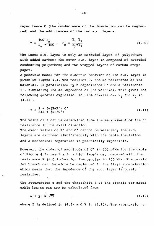
capacitance C (the conductance of the insulation can be neglected) and the admittances of the two s.c. layers:
y y s (4 .10)
The inner s. c. layer is only an extruded layer of polyethene
with added carbon; the outer s.c. layer is composed of extruded
conducting polyethene and two wrapped layers of carbon crepe paper. A possible model for the electric behavior of the s.c. layer is given in Figure 4.4. The resistor R, the de resistance of the
material, is parallelled by a capacitance C' and a resistance R', simulating the ac impedance of the material. This gives the following general expression for the admittances Y1 and Y2 in (4.10}:
y = i + jw(R+R'} C' R(l + jwR'C'} (4.11)
The value of R can be determined f rom the measurement of the de resistance in the axial direction. The exact values of R' and C' cannot be measured; the s.c. layers are extruded simultaneously with the cable insulation
and a mechanica! separation is practically impossible.
However, the order of magnitude of C' (> 800 pF/m for the cable of Figure 4.3) results in a high impedance, compared with the resistance R (< 0.1 ohm) for frequencies to 200 MHz. The parallel branch can therefore be neglected in the first approximation which means that the impedance of the s.c. layer is purely resistive.
The attenuation a and the phaseshift f3 of the signals per meter cable length can now be calculated from
a + jf3 = rzy (4.12)
where Z is defined in (4.4) and Yin (4.10). The attenuation a
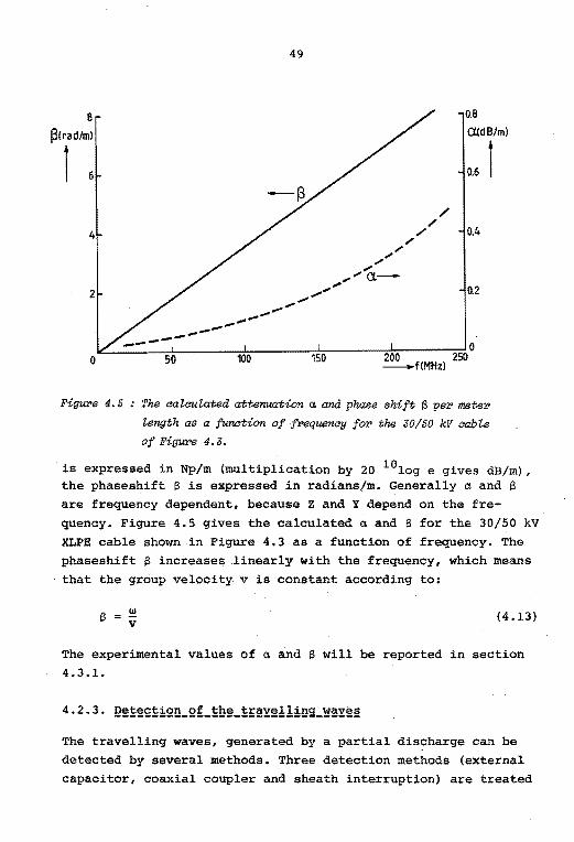
8
~lrad/m)
î 6
4
2
Pigu!'e 4.5
49
0.8
Ct.(dB/m)
0.6 î
0.4
0.2
The ealculated attenuation a and phase shift S per meter
'lertf!th as a funetion of f:r-eqU87'/.Cy foP the 30/50 kV cabte
of Pigtl.!'e 4. 3.
is expressed in Np/m (multiplication by 20 101og e gives dB/ml , the phaseshif t B is expressed in radians/m. Generally a and B are frequency dependent, because z and Y depend on the fre
quency. Figure 4.5 gives the calculated a and B for the 30/50 kV
XLPE cable shown in Figure 4.3 as a function of frequency. The
phaseshift e increases linearly with the frequency, which means
that the group velocity v is constant according to:
(4.13)
The experimental values of a and e will be reported in section
4.3.l.
The travelling waves, generated by a partial discharge can be
detected by several methods. Three detection methode (external
capacitor, coaxial coupler and sheath interruption) are treated

50
in section 4.3.2. In this section a fourth detection principle
will be briefly described.
Hz -
Figu:pe 4.6 Earth sereen of the 30/50 kV aable with the measuring aoil.
Most XLPE insulated cables in the voltage range up to 50 kV do
not have a lead or aluminum sheath but have an earth screen of
spiralled copper wire and a copper tape running in the opposite
direction. The spiralling of the wires causes a current in the
•-direction {see Figure 4.6) which in turn causes a magnetic field in the axial direction, Hz. This field can be detected with a simple coil, a number of turns wound around the cable.
If the amplitude of the travelling wave is e, the discharge current in the earth screen {and conductor) is given by:
i "(4.14)
If the assumption is made that this current flows orily through
the spiralling wires, the magnetic field is given by:
i îi (4 .15)
where h is the pitch of the neutral wires, see Figure 4.7. The
measuring coil has N turns, the induced voltage Vind is then given by:
d~ N dt (4.16)

51
21Tr
Figure 4. 7 Definition of the pitah {h) of the neutra.'t 1'Ylres.
From (4.2), (4.14) and (4.16) the relationship between Vind and the discharge magnitude can be calculated:
(4.17)
An integration of this induction voltage would give a signa!
proportional to ib (compare (4.2)) which can be readily compared to partial discharge signals obtained by other methods, for
instance the sheath interruption method.
The effect of the current in the spiralling wires is counteracted by a current in the oppositely wound copper tape. How the discharge current is shared between the wires and the tape depends on the respective selfinductances, on the mutual inductance between the wires and the tape and on the contact resistance. Especially the uncertainty about the contact resistance
between wires and tapes makes it difficult to predict the sen
sitivity of the measuring coil. The described detection coil would have a number of advantages: no damage to the cable and directional sensitivity. No extensive expèriments have been carried out up till now, due to the above mentioned difficulties.

52
The sensitivity of discharge detection usually refers to the smallest partial discharge (in pC) that can be detected. For
narrow band detection systems_ the sensitivity for large objects is in the order of 0.1 pC under favorable conditions. For the calculation of the sensitivity in a wideband detection system the theory of optimum detection systems, developed for radar
systems is useful [Bo 82].
The cable and the pd detection system can be considered as linear transfer systems, see Figure 4.8. The transfer function of the cable is derived in section 4.2.l. The transfer function
of the detection system can be chosen as to match the signals
from the cable.
partial discharge cable detection system (filter)
measured valve
Fi(JUX'e 4.8 SignaZ path from partiai disaharge to measured value. The
aable and. the deteaticm system are aonsidered as transfer systems.
A partial discharge generates a voltage pulse e between conductor and sheath of the cable, according to (4.2). The fre
quency-dependent attenuation of the cable changes the signal to v(t). If the detection system is ideal, th.e sensitivity is determined by the minimum permissible signal-to-noise (power)
ratio, p:
p (4 .18)
where E is the energy of the pd pulse:

53
(lO
E = .!_ f v2 (t) dt zo _.,.
(4.19)
and SN is the noise power per Hz bandwidth Iwa 62]. Equation
(4.18) is only valid when a so-called matched-filter is used for detection; a filter with a frequency dependent pass band
matched to the incoming signal. Since a matched filter is
difficult to realize, it is more convenient to use a rectangular
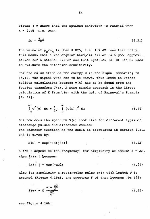
bandpass-filter. The ratio pR/pM, where PR and pM are the S/N ratios for the rectangular and matched filters respectively, can be calculated [Wa 62] and is given in Figure 4.9 for a rectangular pulse of pulselength T (see Figure 4.lOa) as a function of X, the product of T and the bandwidth. Aw of the filter:
X = A~T = ~ Af T (4.20)
0.6
0 2 3 4-x 5
Figure 4.9 : Compariaon of the nctangulaP bandpasa filter (S/N ratio
pR) with the matched fitter (S/N ratio p~ for a rectanguZar
input puZae of Zenf!th T. On the ho!'izontaZ azia the product
of ba:ndhiidth and puZse length X = 6!.ii!/2.
54
Figure 4.9 shows that the optimum bandwidth is reached when X ~ 2.15, i.e. when
llw = 4 • 3 (4.21) '1'
The value of pR/pM is then 0.825, i.e. 1.7 dB less than unity. This means that a rectangular bandpass filter is a good approximation fora matched filter and that equation (4.18) can be used
to evaluate the detection sensitivity.
For the calculation of the energy E in the signal according to (4.19) the signal v(t} has to be known. This leads to rather tedious calculations because v(t} has to be found from the Fourier transform V(w). Amore simple approach is the direct calculation of E from V(w) with the help of Parseval's formula [Pa 62]:
1 27T f IV(w) 1
2 dw (4.22)
But how does the spectrum V(w) look like for different types of discharge pulses and different cables? The transfer function of the cable is calculated in section 4.2.1
and is given by:
H(w) = exp{-(a+j$)1} (4.23)
a and $ depend on the frequency: for sirnplicity we assume a = aw,
then IH!wl 1 becomes:
IH!w) 1 = exp(-awl) (4.24)
Also for simplicity a rectangular pulse e(t) with length T is assumed (Figure 4.lOa), the spectrum F(w) then becomes [Pa 62]:
F(w) sin wT
T -~-=-2-wT 2
see Figure 4.lOb.
(4.25)

55
-T/2 T/2 -t
(a) ( b)
FiguPe 4.10 Sha:pe of the input puZse e(t) (a) and aoPPesponding
speat!'UTll F(w) (b).
From (4.24) and (4.25) the spectrum V(wl can be calculated:
IVCw) 1
wT sin 2 -awl
T wT e 2
(4. 26)
The phase shift of the signals is ignored in (4.26). Figure 4.11
gives a picture of IVCf) 1 for different values of the pulse
length T. A cable length of 30 mand a value for a of 2.5 * 10-9
dB/Hz.m was assumed, corresponding to Figure 4.15. The only in
fluence of the rectangular bandpass characteristic of the de
tection system is a limitation of the spectrum to ± ~w.
From (4.19), (4.22) and (4.26) the energy of the signa! after
passing the cable can be calculated as a function of the pulse
length T. The resul t is gi ven in Figure 4 .1.2. The reference is
the energy of the original signa! (not attenuated by the cable)
with the same amplitude. Especially short pulses are strongly
attenuated by the cable.
The preceding calculations and Figure 4.12 provide sufficient
information to calculate the minimum detectable partial discharge. The available thermal noise power per Hz bandwidth at 290 K is given by:

56
--T= 1ns -·-T= Sns -+-T= 10ns ----T= 20ns
0.4
0.2
·--·-·-·--·
Figu:t'(il 4.11 Speat'l'W11 V(f) for reatangular puZses of various puZse
widths, after attenuation by 30 meters the of 30/DO
XLPE aabZe under aonsideration.
S == kT " 4 * l0-21
W/Hz N (4.27)
Although a S/N ratio of 0 dB is acceptable when the discharges are displayed on a CRT the losses of the detection system (coupling losses) and the extra noise of the amplifiers have to
be taken into account. The coupling losses can be as high as 10 dB ([Bo 82], see also section 4.3.2), while a practical wide band amplifier adds 5 - 10 dB noise. Therefore the minimum acceptable S/N ratio is set to 20 dB here. This leads to a
minimum signal energy of 4 * lo-19 J.

57
10~1 ....,,..__.~---'---'-'-'""'-:-~"'-~.i...... ................ ,,.__...~__.__.__,_, 106 101 102 _ t<nsl 103
Figure 4.12 : Energy aontent of the ol'iginc(l and the attenuated pa!'tial
disaha'l'(Je pulse as a f;mction of the pulse ûlidth. The
amplitude of the inaoming pulse is 1 Volt (across 34 Q),
the pu'l,se ûlidth T.
With Figure 4.12 and equations (4.2) and (4.3) the minimum de
tectable signal can be calculated in terms of charge. The results are given in Figure 4.13 •. The lower curve gives the sensitivity in the case of no attenuation, the upper curve gives the values with the attenuation present. The sensitivity (for this type and
length of cable!) is clearly limited to 0.05 pC.

58
q !pCl ....__ _ __, __ --+_ -+-~f--1-----+~-
î
0.001~ _ __.. __ _.__..__...._..__ _ __. __ _.__~~~-~~-~-~ .......... 1 10 100 - T !nsl 1000
Figure 4.13 The smai'lest dBteatabl.e partiaZ. diaaharge vs puZ.ae Zength
for 30 meter of the XLPE aabl.e under aonsidBmtion.
The Figures 4.11 and 4.13 also give an indication for the op
timum bandwidth of the detection system. Equation (4.21) gives
for a l ns pulse a bandwidth of 680 MHz, while Figure 4.11 shows,
that the spectrum is falling rapidly above 300 MHz. Also Figure
4.13 confirms that the cable itself limits the propagation of
very short pulses rather than the detection system.

59
The practical situation can deviate from the precedin9 theory on two important points:
- the pulse form of an actual pd is usually not rectangular. However, the results with other pulse forms will not differ
much from the results obtained here, see e.g. !Bo 82].
- the different locations of discharge sites result in different distances to the detection point. As the attenuation is a function of distance, the same pd si9nals at different sites have different spectra upon detection. This fact can hardly be
accounted for in theory.
To conclude this section some remarks should be made about
further enhancement of the S/N ratio. The application of corre
lation techniques to pd measurements was first reported by Wilson {Wi 73]. The primary tecbnique is signal avera9ing, although auto- and cross-correlating can also be used {Be 71].
However, there are a number of problems involved in signal
averaging:
- a partial discharge is a random process [Be 71]1 the avera9ing can only be successful if the repeatability of the discharge in each cycle is sufficiently high.
- The repetition rate of the pd signals is.50 Hz. The enhancement of the S/N ratio is proportional to the number
of repetitions [Tr 68]. This means fora 20 dB improvement already a measuring time of 2 s.
- The situation gets worse for a wideband detector. The limited time resolution of a multichannel averager requires the use of a boxcar averager here. A boxcar averager is in fact a single channel averager, which only takes one sample per period. This
. . elongates the measuring time by an order of magnitude [Wi 73].
These problems make it clear that signa! correlation techniques cannot really improve the S/N ratio in pd measurements significantly.

60
4.3. Experiments
4.3.l. ~~ê§~~~~ll~§_Qll_Èh!_EEQEêgêÈ!2U_Q!_b!_2!gnê!§_!u_EQ~~E
!:ê!:!!~§
The attenuation and phase shift of hf signals were measured on the 30/50 kV cable shown in Figure 4.3. The cable is terminated
with its characteristic impedance (34 0), composed of 10 discrete low inductance resistors in parallel. The measurements were carried out with a HP 8405A vector voltmeter and a HP 8654A RF generator; the experimental set-up is given in Figure 4.14.
signal generator
XLPE cable l34Ql
HP840SA
vector voltmeter
Fi(!U't'e 4.14 : Teat aet-up fo~ the attenuation meas~ements.
The transition in characteristic impedance from the 50 0 of the signal generator cable to the 34 n of the XLPE cable gives rise to a reflection of about 17% of the signal. This does not influence the measurements because both incoming and outgoing signals are measured with high impedance (100 kO, 2.5 pF} probes. The attenuation per meter cable length as a function of frequency is given in Figure 4.15; The measured values are significantly higher than the values calculated in section 4.2.2. This can be due to the fact that the properties of the s.c.
layers were unsufficiently known. The measured attenuation of 2.5 * 10-9 dB/m.Hz happens to be in good agreement with the value measured by Stene and Boggs [St 82] for a similar type of
cable.
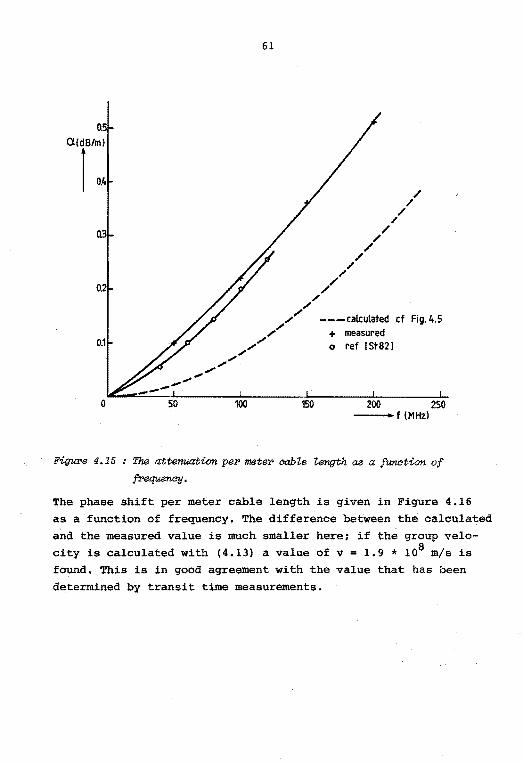
05
Q3
0.1
---_ ....
0 50
; ,,,...,,,,.
61
,,,."" ;""'
,,/''
100
/ /
// /
/
/ /
/
/ /
/ /
/
// ---calcutated cf Fig. 4.5
150
+ measured o ref ISt821
200 250 -t!MHzl
Figure 4.15 The attenuation pel' metel' cabZe Zengt;h aa a fu:n.ation of
fr'equency.
The phase shift per meter cable length is given in Figure 4.16 as a function of frequency. The difference between the calculated
and the measured value is much smaller here~ if the group velocity is calculated with (4.13) a value of v = 1.9 * 108 m/s is found. This is in good agreement with the value that has been determined by transit time measure.ments.
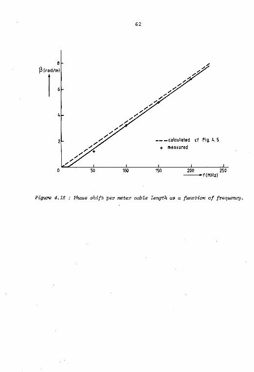
8 ~(rad/ml
1 ' 4
2
0 50
62
100
---calculated cf Fig. 4. 5
+ measured
150 200 250 -f(MHzl
Figm>e 4.16 : Pha8e shift per meter aabZe length as a funetion of frequenay.
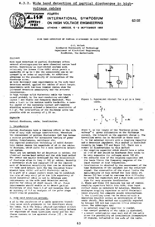
4.3.2. !!g~_è2ag_g~~~2~!QB_Q~_2!~~!ë!_9!!2hë~g~!-!B_h!ghYQgëg!_2ë!?!!iH\l
FOURTH
INTERNATIONAL SYMPOSIUM 63.02
WIDE BAND DETECTION OF PARTIAL DISCHARGES IN HIGH VOLTAGE CABLF;S
<:<.G. Wolzak eindhoven University of Technol~
Department of Electrical En9ineerin9 Eindhoven, The Netherlands
Abstract
Wide band detection of partial di scharges offers several a.dvantacres over the more classical narrow band method~ Especially in distributed systems with relati vely low losses ( like GITL) which permit a bandwidth of up to 1 GHz the sensitivity can be increased by an order of maqnitude. An additional advantage is the possibility of localization of the discharQe sites. · we have developed some il!ll?r<•ve:""'11ts on the wide band detection methodr cables of short length. C::xperiments wi th coax.ial cab les show the increased detection sensitivity and the accurate localization. In high voltage solid dielectric éable the losses -caused probably by the serui-conducting extruded layers - are higher anö dependent. Thia sets a limit to the maximum bandwidth. A. care-ful layout of the measuring circuit and numerous shielding measures allawed a detection sensitivity of 0.1 pC. The localization of the discharge sites was possible wi th an accuracy of :!: 20 cm.
Keywords
Partial discharge, cable, localization.
1. Introduction
Partial discharges have a lfmi ting effect on the life time of many high constructions. Therefore the measurement of discharges (pd) has become: a routine procedure testin9 of power cables, transformers, etc. The improved production of solid dielec-tric cables causea the pd. in the cables to decrease, which a more sensitive detect-ion system. There are two methods for pd detection in cables: the classical narrow band method and the wide 'band method The latter was mainly developed for the localization cf discharge sites in long (> 500 m} cahles. Recently a systematic study waS [ l) on the improve-ment of detection that can be obtained by thè wide band method, both Gas lnsulated Trans-mission Line (Gl'fL) and solid dielectric cable. As a part of a largar which has to establish the role of very on the life expectancy of solid dielectric cahle we had to develope some irnprovements on the wide band detection methodt applied for cables of short length (30 m). These improvements should enable us to detect partial discharges of less then O.S pC and localize then with an accuracy cf O. S m; analysîs of the pulse shape should also be possible.
2. Wiàe band detection methóds.
A pd in the insulation ling waves which thB cable. Wi t.h
of a cable generates travelin two directions ;dong adopteà equivalent circuit
the relationship between t.he amplitude of these ti.avelling waves and the discharg~ current or the apparent charge [2] . We can derive:
63
b
e
Figure l. Equivalent circuit for a pd in a lonç cable.
z e= f 1 ())
T T r 1b 2 f0
e.dt (2) q; :z 0
0 0
=~:;0 !s :i:es of the ~!s::r~~s~!:~ The
current, the inteqral on the apparent charge q~ The travelling waves can be detected in three ways; 1. In the external circuit with a coupling capacitor and a detection impedance" This method is describeà recently by Lemke [3] and Beyer [4]. There are a rumbér of disadvantage:s to this method:
the coupling capacitor which should have a value of 1 ... 10 nF and should be discharge free tends to be very expensive for voltages above 100 kV, the physical size of the coupling capacitor and its leads limits the response of the input circuit at
- localization is
signa!. The attenuation of the signal linti ts the applicability of this methód for very small pd. Reeves {S] has tried to overcome this àifficulty by using two capacitors and a dual beam oscilloscope for very accurate localization.
2. Boggs and Stone [ 1} describe the use of coaxial coupling capacitors built into GITL; this input circuit shows an excellent hf behavior. However, an analogous coupling capacitor in solid dielectric cable two complete sheath :i,nterruptions. 3. The waves èan be detectea with a
across an interruption of the cable sheath. This rnethod was originally by KreW)er [2] but has reçeived li ttle s.ince~ '!'he advanta9es are: - no externa~ couplin9 capacitor is needed, - the coaxial of the cable .is u••••>"~·•v., - a sheath near each end of
gives the of localization u:reeipectJLve at the ends of the

We have adopted this last method for the detection of small pd in short cab les.
3~ Description of the measuring method.
3.1. Theory.
V???? 2? 222 ·sheath
n1 i- l. dielectric
lel r:a [û] ... •--e"...,r-"_1,..,"----u~r----• conductor
Z???Z??Zr~z-·_,~,....i....,~v-'i?ZZZZZ?Z
~ v :
Fiqure 2. Siqnals at a sheath interruption.
A picture of incident, reflected and transmitted signals at an interruption of the cable sheath is given in Figure 2. Important for pd detection is the relationship between the voltage across the measuring impedance zm and the original wave amplitude et
v 2-e. (3)
The measuring impedance z can be formed by a discrete resistor, the resis~ance of a serniconductin9 layer or the input irnpedance of the measuring system.
In the more refined equivalent circuit of Figure 3 we have included the 1 ground-impedance' z 9 , the wave impeda:nce of the cable sheath with respect. to the nearby ground plane.
2Z +
v
Figure 3. Equivalent circuit of sheath interruptiorL
With this change <'.n turns into:
v"" 2e z
m Z + 2Z
m o (1 + z )
m z g
14)
With two sheath interruptions in a cable, one at each end, the following detection circuits are possible:
straight detection at one interruption can be used for analysis of the pd pulse shape~ For localization one of the two following circuits has to be used.
- detection with two interruptions in Fi9ure 4a. The- equivalent circuit is Figure 4b~ balaneed detection, see Fiqure 4c. The measuring cable wi th characteristic impedance Zm is connected between a. en b. A balun (balanced-~balanced
64
transformer} has to be used to match the diffe,ren-tial voltage to the asynµnetric measuring cable and amplifier
2Zo a b 2Z
{cl
Figure 4. Poseible measuring circuits: (a} cable and sheath iriterruptions {b) unbalanced detection# equivalent
circuit (c) balanced detection, equivalent circuit The two voltage sources in (b) and (c) represent the inc{dent wave fronts which may arrive at different moments.
The balanced circuit can be used for the supp;ression of external interference. Howeve:r, this advantage is only fully exploited when the remaining cable lengths beyond the interruptions are equal and the high voltage connection (point d. in Figure 4.a) is located halfway the two terminad.ons; only then the transit times of the interfering signals to the interruptions are equal so that they do not show up in va - vb.
}.3. Localization.
Localization of a discharge site in the cable between the interruptions is possible by the measurement of the time difference of the. pulses, arri ving at the interruptions. In -cwo cases this procedure can give some difficul ties: - a pd located in the middle of the cable
does not register the balanced àectection set.-up, because the two arr'ive at the inter-ruptions problem is to r:ieasure two signals and a dual beam oscilloscope or wi th the balanced setup.
- a discharge si te in the immediate vicini ty of a sheath interruption leads to more complicated
because reflections from the terminations quickly" In the inte.roretation one should
notè that the of thé measured pulses depends on the in which the wave propa-9ates.

The length o f the cable between the interruptions can e a s i l y be d etermined by the injection o f a simulated d i s c ha rge pulse a t one interruption which is then 1t:easur ed a t both interruptions. The reflected signa l s fro w the t e raüna t ions shou l d no t i n t e rfere with t.he direc t signal s . This c an be achieve d when the shc d t h i nte r r uption s are at a suff i ciently large d i ::; t a nce from the terrni nations. A length of 2 to 3 me t e r s cable i s enough.
4 . Appar.:itus.
All meas urernents were carried out in the .::i hielded h t gh vo ltage laboratory of the Eindhove n Uni versi t y of Te chnolo gy. The excellent shielding of th i s laboratory gi ves a 80 dB damping of unwanted si g na l s .
F'or ·~ h e od rneasurernent we used a Tektroni.x 7844 dual bt..: .11:1 osci.11o scope with a bandwidth of 400 MHz. The o~c illoscope w<is placed in a small shielde<l rDCöS uring cabi n . The mcasuring t:z..l.ble (RG 214 U) is laid in a c o p i;:e r pipe . The characteristic irnpedance of t hl s t erm.i.nated Cd.ble farms the input i mpedance of the n:o:·a sur ing s yst•'l!i . Me d s urement of very small pd. is r ossible by the u se oi Avantek pre -amplifiers . l<fe used t1~0 t ypes .. with ba ndwi d ths o f 2 MHz - 550 MHz and 200 Hz - 550 MHz. ·r h 0 g i::li n o f both t ypes was 28 dB and the ir noi!le SJ "v ff" The smallest detecta.ble sig na! was the re f o re Ïso µV pp· Severa l t ypes of balun were used, c o n s t r uc t e d accord i nq t o (6). All had a small f erri t e t o r o i d al c a r e, with 7 to lJ turns o f wire on it.
5. E:xperlments.
5 .1. Tests with RG 214 U a nd RG 218 U ca.bles.
These cables, wi th a characteris tic i ropec:!4 nce z0
= 500 were used for calibration and in lti al t es ts . Simulated discharge pulses were i n jecte d in to a cable wi th no terminations; from t he signa ls measu red at the interruptions we were able t o c alculate t he qround impedance z
9.
For this cable and lnterruptions, z9
wa s abou t 2000 . The very small dam.ping of the cables caus es lit t le attenuation or distortion of the pè s igna is. The re fore we were able to measure very small di sch a r q e s and locate thew very accurately. fiqu r e S g i ves a picture of a pd in a RG 214 u cable . The di s cha r ge magnitude was 0.44 pC and the detection c i rcuit of F igure 4. b was used.
FirJure 5. Parcia! discharge in a RG 21 4 U c a.b l e .
Tlw l nngth o r t he cJ\b lc was 20 m; t.h l'! LOC'Ul.iz a tJ~;in of ·ha rJ1.scri<H g e •i u \<tas pos~lble '../ i t.h a n accuracy of
..: 3 (;lli .
7'.,e smö l lust pel wu r1 a v1J observc::.l i n th ls c.:ib l e was 0 . 0~ fL , wi th · l pu l i10 dut·.;i c:1cn of 5 na . '.-Ji t h C2i and (4) wé <:: Ft n c&L~u ln <J , h a t tl1ir. i.r. J"i ~t <1bovP t h 'thc u r t H:-0.l rn.i.M.LUUlln (0 , Q)- nC ) fo r lhC Çi ven ~Ul i:C
lenq h .
65
5 . 3 . Tr,~ ts wi th 30/ 50 kV XLPE c 4ba!: .
These power c ables have a cha racteris U c irnpedance of about J 4Q, Shea th i n t.er rupti orn: a re mttdc in the c opp er wi r e s o f the gr ound h ield. The outer serniconduc ti ve layer then g ive s d mca suring resistance of 500 t o 10000, pa r alle l t o the 50 i nput impedance of the measu r in9 s ys t em. A number o f t o sts wi th s imulated dis charge pulses s ho wed th t c able s to have a r a ther h i q h at. tenuation o f hf s lqnn ls . 'thi s can p roba b l y be atcributed to th€ sern.ico nductive l a y c r s- [ 7]. The deta ilc 1 re su l ts o f the a ttenua tio n :neacuremen t.s and ca lcula t ion s wi il be r e por t e d i n the nea.r t! u ture.
f'igu r e 6. Part i al discharge in a J0/50 kV XLPE cable.
A t y p ical e xarople o f a pel in the XLPE cab l.e is given in Flgure 6. Si gna l:=:! of this k ind are d i f ttcu lt to integrate fo r the mea s u reme n t. o f t he apparent charge q. We therefore ha ve used a c onve n tional ERA- : dete c to r for r efer ence measuremen ts . The s mallest discharge we ha ve obsc rvcd in he po\./e r c abie s was a 0 .4 pe , 10 ns pulse. Thü; di s c ha.rge coul d be l ocalized wi th accuracy of !. 20 c m.
6 . Conclusion .
The experiments have shoW"TJ t hat wide ba.nè detectio n of partial discharges i s pos sibl e i n shor t h i gh vol t aqecab l e s with s olid d i ele ctr l c . The los ses in the extrud d inner and oute.r s em.i c onducti ve layers lirni t the maximum usable bar.chl i d t h t o abo u t 100 MHz. A number of sh i.c: lding precaution s c a n b rin9 d o wn the IT:@as uring sens itivity to l !!SS t.han O. !i pC . Wi de band dete ction ma kes locaU za t l o n of di~cha rge
Gl tes posf:i b l e . In the pape r thi~ wa a. dons by os ci lloscope rneu 1,1 reme~ts , b\l t th o u::; of mo r e advanced ü l c ctronics is possib l.e ,
7 . ALkno-.... ledljléralln t .
T h e. author th<1 nKsi p rof . .r .C. T. v ,;ui d·~ r Lna n fo r h u; constan t i n t .erest and encour dgernent: . He ack nowlé'dges
he. he l p of E. f· . StC!ennis i.n e n ear lier part of t h e work. The measu r i..n g methöd ,,... ts devalopccl n s it p.irt cf a r l?'.Elea rch co:"l t. ract w:. h KEMA, Th e Ne be r lo.ods.
8 . Refe rences .
{ l ) Boqqs , S . A., Som:~ , G .C. · "f'lmtlttr.:ontnl .ll.mita t:lons in cilc rr..ea.sur emen t o f cor o na and p a =: t i a l d i scha ~ ".
IlE 'l'tansac t i.ons vol El 17 (~ 982 ) pp 14 3-150. [ 2 ) Kreuqe r , F .H . : '' Di.scha r qe d e t ection in h i.Qh
volt.n.ge equipment " . llPJ"" , ~ndcn , 1964. [3] L-eoke, e . · " A nE-w Cie t hod Co r: pd cueasurement:. on
pol.yct.h y 1c nr: i n .:;u l..:1 rtd f>OW!3 r c.;i.h lrs " . Jn1 ! n te'tnaciona l :.-;ymponium n Hlqh Vo lt. pg Enr; i neednq , Milan , I aily . 8-3 1 AUQU1Jr 1 79 ,
a p•""r 4 1 . 13 .

(4] Beyer, M., Borsi, H. 1 Feser, L new method for detection of geo-metrically distributed partial discharges {cable faults) in high voltage cables under external interference". CIGRE SC 15 Colloquium.Liège, Be1-9ium, 24 August 198!.
[5] Reeves, 3 .H.: "The location of partial discharge sites in h~v~ switch9ear and short cables by a travellinç wave method" w
C!nt::D, Brighton, UK, 1-5 June 1981, paper 4.12
66
[6] Ruthroff, C.L.: "Some broad-band transformers••" Proceedin9s of the IRE, vol 47 (1959) pp. 1337-1342.
[7] Stone, G.C., Boggs, S.Aw: discharge pulses in
CEIDP, Amherst, 17-21 October 1982, pp. 275-280.
67
REFERliHl!:S
[Be 63] Bewley, L.V. Tl'C-DIMl!N)ICH\L FIEUE IN ELl1Cl'1UCAL ENGINEERING. New York: Dover, 1963. Reprint of the 1948 ed.
[Be 71] Bendat, J.S. and A.G. Piersol ~ DATA: Analysis and measl.lI'E!mi:!t procedures. New York: Wiley, 1971.
[Bo 82] ~' S.A. and G.C. Stone FUNOAMENTAL LIMI'mTIOOS IN mE ME'A'3UREMENr OF COlOilA AND PARTIAL DlsaIAIGlS. IEEE Trans. Electr. In.sul., Vol. EI-17 (1982), p. 143-150.
[Br 711 Breien, o. and r. Johansen ~00 OF TRAVELLING WAVPS IN SINGLE-PHASE HIGi-VOL'mGE CABLES. Proc. Inst. Electr. Eng" vol. 118(1971), p. 787-793.
[ca 75] carlson, A.B. CCM1UNICATIOO SYS'lD!S: Àn intl:oduction to signals and noise in electrical o:mrunication. 2n1 ed. New York: M::Gt'aw-Hill, 1975. M::Graw-Hill electrical and electronic engineering series
[Du 78] ~, R.C. and W.L. $p0nsler SURGE P~ OF UD CABLE SYS'ID!S. Part 2: Analytical rrodels and sinulations. IEEE Trans. Power Appar. & Syst., vol. PJ.\S-97 (1978) , p. 1901-1909.
[G:> 40] Gohlke, w. uOO u. Neubert BEMERKlJtl>EN ZUR HOOi- UNO HOcHs'l'SPANNllliGSM&SSUN. Z. Tech. Phys., Vol. 21 (1940), p. 217-222.
[Gr 69) Groenenboan, M. en H.A.J.M. Spcx>renberg DE ESPCM: F.ell capacitief gekoppelde elektronische spanningstransfornator. Smit ~., vol. 24 (1969) , p. 223-232.
[m 79 J CXJMNl'ICNAL 1\ND tJNO:WEm'IAL CURRENT AND VOLTAGE 'l'RAN.SFORMERS WITH PARl'ICl'JIAR REFERENCE TO USE WI'lH SOLID S'mTE DEVICES. Proc. C.011., I.ondon, 26 Jan. 1979. I.ondon: Institution of Electrical Engineers, 1979. IEE C.Olloquia Digest No. 1979/7.
[Kä 76 J Kärkkäinen, s. INl'ERNAL PARI'IAL DISCHARGES: Pulse distributiorui, physical mechanisms and effects on insulations. Ph.D. Thesis. Helsinki University of Technology, 1976. Espcx>: Technical Research Centre of Finland, J.976. Electrical and nuclear technology publication, 14.

68
[Ke 64 ] Keller, R. WIDElWID HIGI VOLTAGE ProBE. Rev. SCi. Instrum., Vol. 35(1964), p. 1057-1060.
(Kr 64] .iu:euger 1 F .H. DISCHJ\RGE IlE'J.'.EI:TIOO IN HIGI VOLTAGE B;JUIPMENT. llondon: Heywood, 1964.
[Iu 79]' IJJczyfiski, B. PARI'IAL DISCHARGES IN ARrIFICIAL G!\S-FILI.ED CAVITIES IN SOLID HIG! VOLTAGE INSUIATIOO. Ph.D. 'l'hesis. Technica! University of Denmark (~), 1979. Electric PcMel:" Engineering Deparbnent, Publication No. 7902.
[Ni 63] Nie, A.(3. van and J.J. Zaalberg van Zelst A VIBRATill; CAPACI'IDR DRIVEN BY A HI<E-FRBJUE!oc:Y El.ECTRIC FIEID. Philips Tec:h. Bev., vol. 25(1963/64), p. 95-103. Dutch version: Philips Tech. Tijdschr., Vol. 25(1963), p. 77-85~
[Pa 62] Papoul.is, A. 'lHE FOURIER IN1'EGRAL AND ITS APPLICATIONS. New York: ?ot:Graw-Hill, 1962. ?ot:Graw-Hill elect:ronic scienoes series
[Pr 69] Prinz, H. HOCHSPANNUNa;FEWER. ttinchen: Oldenbourg, 1969.
[St 82] Stone, G.C. and S.A. ~ POOPAG!rn:CN OF PARI'IAL DISCHJ\RGE PCJI.SES IN SHIEl:DED l?OOER CABI.E. In: Annual Report 5lst conf. on Electrical Insulation and Dielectric Phenanena, Amherst, Mass., 17-21 Q::t. 1982. Piscataway, N.J.: IEEE Service Center, 1982. P. 275-280.
[To 82] 'lbkoro, K. et al. DEllEWPMEN'l' OF ELElC'l'.R'JNIC l?OTENTIAL AND CURRENT TRANSDOCERS SUI'l2\BIE FOR GAS INSUIATED sw.rn::HGE'AR AND A!lB;lUATE FOR APPLICATIOO TO StJBS'I2.\.TIOO DIGITAL CCNI'ROL SYS'l'.EMS. IEEE Trans. ~ Appar. & Syst., Vol. PAS-101(1982), p. 3967-3976.
[Tr 68] Tri.mble, C.R. WRAT IS SIGNAL AVERAGING? Hewlett-Packard J., Vol. 19, No. 9 (April 1968), p. 2-7.
[Wa 62] Wainstein, L.A. and V.D. Zubakov Elcr.'RACTIOO OF SIGNALS FRCM NOISE. Englewood Cliffs, N.J.: Prentice-Hall, 1962. Translated frcm Russian.
['*' 81]
[Zi 32]
69
W::>lzak, G.G. and P.C.T. van der Iaan DISCUSSICN CN '!HE JU,JIVAIBNT CIIOJIT OF A PARI'IAL DISCHAR:iE: Possible new measurement techniques. Paper presented at the Coli. of the CIGRE Study ccmnitte 15 {Insulating Materials) on the Detection and Effects of Partial Discharges in Insulating Materials, Liège, 24 Sept. 1981. Abstracts in: Electra {Paris) , No. 80 {Jan. 1982), p. 43-45. Full text obtainable fran the authors: Department of Electrical Engineering, Eindhoven university of Technology, Netherlands.
Zisman, W.A. · A Nm ME:IHOD OF MFASURING <XNl'ACT POl'ENTIAL DIFFERENCES IN METAIS. Rev. Sci. Instrum., Vol. 3(1932), p. 367-370.

70
SAMENVATTING
Dit proefschrift beschrijft de ontwikkeling van enige meetmetho
den op het gebied van de hoogspanningstechniek. Hierbij ligt het
accent op meetmethoden voor hoge spanning en op detectiemethoden
voor partiële ontladingen.
voor het meten van hoge, spanningen zijn twee methoden ontwikkeld,
beide met als ingangscircuit een enkele hoogspanningscöndensator.
De eerste methode wordt beschreven in hoofdstuk 2 en is gebaseerd
op achtereenvolgende differentiatie en integratie van het sig
naal. Een belangrijk voordeel van deze methode is, dat tussen
hoogspanningsdeel en meetinstrument een lange coaxiale meetkabel
gebruikt kan worden. Deze karakteristiek afgesloten meetkabel
vormt dan een integraal deel van het meetsysteem. Op basis van
dit principe zijn verschillende uitvoeringen gerealiseerd voor
het meten van gelijk-, wissel- en stootspanningen~ de resultaten van de metingen met deze apparaten worden ook in hoofdstuk 2
beschreven.
De tweede methode van spanningsmeting is een moderne uitvoering
van de genererende voltmeter. In hoofdstuk 3 wordt een voltmeter
beschreven die geen roterende maar een vibrerende meetelektrode
heeft, aangedreven door een piëzo-elektrische transducer. In het
kort worden de mogelijkheden aangegeven dit apparaat te gebruiken
voor het meten van spanningen en elektrische velden. Tevens wordt
een beschrijving gegeven van de benodigde apparätuur om het ge
moduleerde signaal van de bewegende elektrode om te zetten in een
spanning die evenredig is met de te meten spanning.
De detectie van partiële ontladingen in hoogspanningskabels is
het onderwerp van hoofdstuk 4. Door een partiële ontlading, ver
oorzaakt door een holte in het diëlektricum van de kabel ontstaan
lopende golven tussen geleider en mantel. Na een kort overzicht
van de vervangingsschema's voor een partiële ontlading wordt de
voortplanting van deze golven langs de kabel nader bestudeerd.
De verzwakking van de lopende golven wordt voornamelijk veroorzaakt door de halfgeleidende schermen (geleider- en aderscherm)
71
aan weerszijden van de isolatie. Het theoretische model hiervoor wordt door middel van verzwakkingsmetingen geverifieerd. Gegeven deze eigenschappen van de kabel is de kleinst detekteerbare partiële ontlading bepaald met behulp van een theoretisch model. Voor 30 m kabel van een bepaald type (30/50 kV XLPE) blijkt deze kleinste ontlading 0.05 pC te zijn. De lopende golven kunnen op twee :manieren worden gedetecteerd: door middel van een onderbreking van de kabelmantel 3f met behulp van een spoeltje dat om de kabel gewonden is. De tweede methode wordt hier slechts kort beschreven. Het hoofdstuk eindigt met enige experimentele resultaten, waaronder oscillogrammen van enige kleine partiële ontladingen in verschillende typen kabel.
72
DANKBETUIGING
Het in dit proefschrift beschreven onderzoek werd uitgevoerd in
het Hoogspanningslaboratorium van de vakgroep "Technieken van de Energievoorziening" van de TH Eindhoven. Velen, in en buiten deze vakgroep, hebben hierbij hun medewerking
gegeven. Prof.dr.ir. P.C.T. van der Laan ben ik erkentelijk voor zijn
voortdurende interesse in en stimulering van het onderzoek. Herrn Prof. Dr.-Ing. K. MÖller danke ich für die bere.itwillige
Obername des zweiten Referates und die rasche Durchsicht des Manuskriptes. De technische staf van het hoogspanningslaboratorium ben ik dank verschuldigd voor de steun bij de experimentele realisatie van het onderzoek. zonder de overige leden te kort te doen wil
ik op deze plaats met name mijn "technische rechterhand" Th.G.M. van Moorsel vermelden. Zonder de financiële en materiële steun van de N.V. KEMA te Arnhem, NKF Kabel B.V. te Delft en COQ B.V. te Amersfoort zou
het onderzoek op deze schaal niet mogelijk geweest zijn. Een belangrijke bijdrage aan het onderzoek werd ook geleverd door mijn afstudeerders ir. J.A.G. Bekkers, ir. E.F. Steennis, ir. H.A. Minkman, ir. W.Chr. van Abkoude en E.J. Bresser. Hier
voor mijn dank, die tevens geldt voor de stagiairs die bij het onderzoek betrokken waren.
Mevr. W.M.L. Marrevêe en mevr. T.J.F.M. Pellegrino typten de tekst voor dit proefschrift; F.M. van Gompel leverde niet alleen technische assistentie bij het onderzoek maar verzorgde ook het tekenwerk. Hen allen dank ik hartelijk. Mevr. M.J. van Megen tenslotte wil ik bedanken voor het ontwerpen van de omslag.

73
LEVENSLOOP
Gerard Wolzak werd op 10 november 1952 gebaren te Oosterbeek. In 1970 behaalde hij het diploma HBS-B aan het Nijmeegs Lyceum. Zijn ingenieursdiploma aan de Afdeling der Elektrotechniek van de Technische Hogeschool te Eindhoven behaalde hij in 1977. Het afstudeerwerk, een onderzoek naar de mogelijkheden voor ultrasonore verstuiving van cesium in een MHD-generator, verrichtte hij onder leiding van prof.dr. L.H.Th. Rietjens. Vanaf mei 1977 tot september 1978 vervulde hij als vaandrig, werkzaam bij de Conunissie van Proefneming van de Landmacht, zijn dienstplicht. Vervolgens werkte hij van september 1978 tot november 1979 als research medewerker in het Hoogspannings Research Laboratorium van NKF Kabel B.V. te Delft. Sinds november 1979 is hij werkzaam in het Hoogspanningslaboratorium van de Technische Hogeschool te Eindhoven, aanvankelijk als wetenschappelijk assistent, vanaf maart 1982 als wetenschappelijk ambtenaar. Zijn werk, onder leiding van prof.dr.ir. P.C.T. van der Laan, leidde tot dit proefschrift.

stellingen
behorend bij het proefschrift van
G.G. Wolzak
1. Bij iedere meting in de hoogspanningstechniek is een
correcte definitie vari het - vaak omvangrijke en onover
zichtelijke - ingangscircuit van groot belang. Het onder
scheid, dat Gallagher en Pearmain maken tussen "voltage
pulse detection" en "current pulse detection" is een voorbeeld van onvolledig inzicht in de aard van het
i:igangscircuit..
Dit proefschrift, hoofdstuk 1
T.J. Gallagher, A.J. Pearmain,
High voltage - measurement, testing and design
(John Wiley, New York 1983)
2. Het door Bahder et.al. voorgestelde model voor de veroude
ring van kabels met kunststofisolatie onder invloed van
het elektrische veld kan niet worden toegepast op moderne
XLPE kabels met hoge bedrijfsveldsterkte.
G. Bahder et.al., IEEE Transactions vol. PAS - 101
(19821 pp. 1379-1382.
G. Bahder et.al., IEEE Transactions vol. PAS - 102
(1983) pp. 2173-2182.
3. Het uitwerken van een "whole vehicle radiated susceptibility
test" aan een voertuig wordt bij hoge frequenties steeds
moeilijker door het sterke richteffect van de antennes. In
dit licht gezien is het frequentiebereik waarover een
dergelijke test dient te worden uitgevoerd volgens SAE J 1338
(10 kHz - 18 GHz} niet realistisch.
SAE Publication J 1338, in: SAE Handbook 1982
(Soc. of Automotive Eng., Warrendale, 1982}.
4. Van de bestaande typen spanningsdelers biedt de differenti
erende/integrerende deler de beste mogelijkheid om als onderdeel van de deler een lange, karakteristiek afgesloten
kabel naar het meetinstrument toe te passen.
Dit proefschrift, hoofdstuk 2.

5. De optredende knik in de stijgende flank van een coronapuls,
zoals deze is gemeten door Zentner, vindt zijn oorzaak in
het meetsysteem en niet in een fundamenteel verschijnsel.
R. Zentner, Zeitschr. angew. Physik
pp. 294-301.
(1970)
6. Gezien de macromoleculaire structuur van polyetheen is het
uitvoeren van een zgn. naaldtest aan dit materiaal te ver
gelijken met het prikken van een scherpgepunte wandelstok
in een emmer, gevuld met rubber ballen. Op grond van de resultaten van dergelijke "naaldtests" kunnen derhalve
geen uitspraken over intrinsieke materiaaleigenschappen worden gedaan.
7. Het model dat door Stone en Boggs wordt gebruikt voor de
beschrijving van een halfgeleidende laag in een hoog
spanningskabel geeft geen adequate beschrijving van de
verzwakking van hoogfrequente signalen.
G.C. Stone, S.A. Boggs, Conf. on El.Ins. and Diel.
Phen., Amherst (1982) pp. 275-280.
Dit proefschrift, hoofdstuk 4.
8. Om een objectieve voorlichting aan de deelnemers van het
"Informatie en communicatie experiment Zuid-Limburg" te waarborgen, verdient het aanbeveling in dit gebied op
ruime schaal Orwell's boek "1984" te verspreiden.
9. De door Nikolopoulos en Topalis aangegeven methode voor het
corrigeren van fouten, veroorzaakt door stootspanningsmeet
systemen, kan onder ongunstige omstandigheden aanleiding
geven tot grotere fouten in het gecorrigeerde dan in het
oorspronkelijke signaal.
P.N. Nikolopoulos, F. Topalis, Fourth Int.Symp. on High Voltage Eng., Athens (1983) paper 65.08
B.R. Hunt, IEEE Transactions vol. AC 17 (1972)
pp. 703-705.

10. De aanwezigheid van oppervlaktelading op een isolerende
spacer beïnvloedt de doorslagspanning van het spacer-gas
systeem. Het is niet correct - hoewel uit praktisch oog
punt begrijpelijk - dat deze oppervlaktelading vaak na het
wegnemen van het elektrische veld gemeten wordt.
L.G. Christophorou (ed.), Gaseous Dielectrics III,
chapter 8 (Pergamon Press, New York, 1982).
ll. De slechte economische situatie in de bouw biedt een goede
gelegenheid de sterk versnipperde structuur - die voor een
belangrijk deel verantwoordelijk is voor de geringe
technische vooruitgang in deze bedrijfstak - te veranderen.
12. De uitvinding van het "scratchen" in de discomuziek dient
te worden gezien als een oneigenlijk middel tot het stimu
leren van de platen verkoop en niet als het toevoegen van
een nieuw element in deze muziek.