Embed Size (px)
Citation preview
The Design of Integrated Switches and Phase Shifters Liam Devlin ∗∗∗∗
Abstract
∗∗∗∗ Liam Devlin is with Plextek Communications Technology Consultants, London Road, Great Chesterford, Essex, CB10 1NY Tel: +44 (0)1799 533200 Fax: +44 (0)1799 533201 Email: [email protected]
Integrated analogue switches can easily be designed using any Field Effect Transistor (FET) based process [1]. The challenges in switch design tend to come in extending the upper operating frequency and/or increasing the power handling capability. The first part of this paper describes the operation of FETs as switches and presents design techniques for realising integrated RF and microwave switches. Consideration is also given to techniques for improving the power handling capability of switch designs. Phase shifting circuits allow control of the insertion phase of a network. They find applications in electronic beam-forming, channel matching networks and measurement systems. The second part of this paper details phase shifting techniques suitable for integrated realisations. Analogue and digitally controlled techniques are included and examples of phase shifter designs are presented.
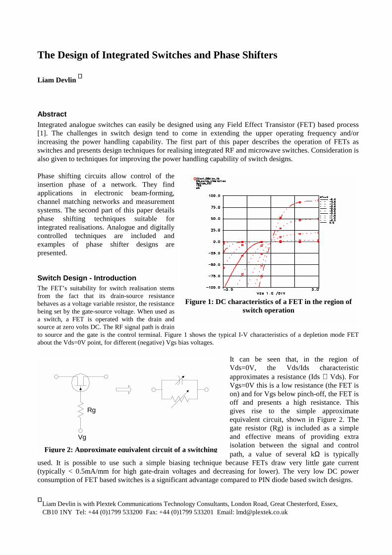
Switch Design - Introduction The FET’s suitability for switch realisation stems from the fact that its drain-source resistance behaves as a voltage variable resistor, the resistance being set by the gate-source voltage. When used as a switch, a FET is operated with the drain and source at zero volts DC. The RF signal path is drain to source and the gate is the control terminal. Figure 1 shows the typical I-V characteristics of a depletion mode FET about the Vds=0V point, for different (negative) Vgs bias voltages.
It can be seen that, in the region of Vds=0V, the Vds/Ids characteristic approximates a resistance (Ids ∝ Vds). For Vgs=0V this is a low resistance (the FET is on) and for Vgs below pinch-off, the FET is off and presents a high resistance. This gives rise to the simple approximate equivalent circuit, shown in Figure 2. The gate resistor (Rg) is included as a simple and effective means of providing extra isolation between the signal and control path, a value of several kΩ is typically
used. It is possible to use such a simple biasing technique because FETs draw very little gate current (typically < 0.5mA/mm for high gate-drain voltages and decreasing for lower). The very low DC power consumption of FET based switches is a significant advantage compared to PIN diode based switch designs.
Figure 1: DC characteristics of a FET in the region of
switch operation
Rg
Vg
Figure 2: Approximate equivalent circuit of a switching
The values of the equivalent resistor and capacitor for a switch FET (Figure 2) are dependent on the process used and the FET size (gate length and gate width). For a 0.5µm gate length, Metal Semiconductor Field Effect Transistor (MESFET) process, the on-case resistance will be around 2.5Ωmm and the off-case resistance about 9kΩmm. Although also shown as variable, the capacitance is normally only of any real significance in the off-case when it limits the high frequency isolation which can be achieved. For the same 0.5µm gate length MESFET process, a value of 0.25pF/mm would be typical. In practice, more complex models are often used which also model the parasitic effects of the terminal contacts.
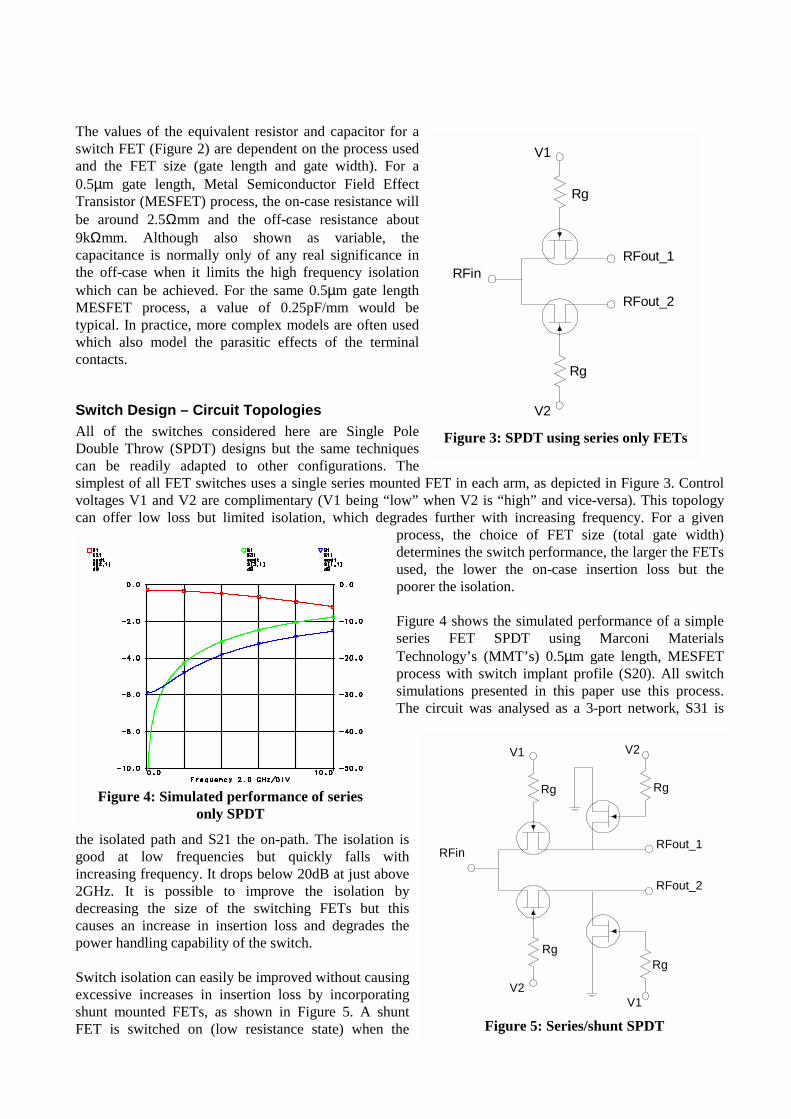
Switch Design – Circuit Topologies All of the switches considered here are Single Pole Double Throw (SPDT) designs but the same techniques can be readily adapted to other configurations. The simplest of all FET switches uses a single series mounted FET in each arm, as depicted in Figure 3. Control voltages V1 and V2 are complimentary (V1 being “low” when V2 is “high” and vice-versa). This topology can offer low loss but limited isolation, which degrades further with increasing frequency. For a given
process, the choice of FET size (total gate width) determines the switch performance, the larger the FETs used, the lower the on-case insertion loss but the poorer the isolation. Figure 4 shows the simulated performance of a simple series FET SPDT using Marconi Materials Technology’s (MMT’s) 0.5µm gate length, MESFET process with switch implant profile (S20). All switch simulations presented in this paper use this process. The circuit was analysed as a 3-port network, S31 is
the isolated path and S21 the on-path. The isolation is good at low frequencies but quickly falls with increasing frequency. It drops below 20dB at just above 2GHz. It is possible to improve the isolation by decreasing the size of the switching FETs but this causes an increase in insertion loss and degrades the power handling capability of the switch. Switch isolation can easily be improved without causing excessive increases in insertion loss by incorporating shunt mounted FETs, as shown in Figure 5. A shunt FET is switched on (low resistance state) when the
Rg
V2
V1
Rg
RFout_1
RFout_2
RFin
Figure 3: SPDT using series only FETs
Figure 4: Simulated performance of series only SPDT
Rg
V2
V1
Rg
RFin
V1
Rg
Rg
V2
RFout_1
RFout_2
Figure 5: Series/shunt SPDT

adjacent series FET is off (high resistance state) and vice-versa. Figure 6 is a plot of the simulated performance of a series/shunt switch. The isolation has increased by around 10dB compared to the simple series FET design but the insertion loss has increased very little. It should be noted that the simulations have assumed ideal grounding for the shunt FETs. Very low inductance grounding can be achieved on many GaAs processes by the use of low inductance, through-substrate vias. However, in order to keep processing costs down, many switch IC manufacturers tend not to make use of through GaAs via holes and grounding must be provided using
bond-wires. The inductance of the bond-wire will obviously degrade the switch isolation, as will any additional packaging parasitics. It should also be noted that the use of shunt FETs can degrade the power handling capability of the design, as explained later. The two switch topologies presented above are both reflective designs, that is the return loss of the off-arm is low. Terminated switches can be easily realised by including a shunt FET and resistor (Rt) at each output, as shown in Figure 7. In the off case Rt will be connected to the output by the shunt mounted FET. Choosing the combined resistance of the FET and Rt to be 50Ω provides a well matched off-case output, this is known as a terminated switch design. If more isolation is required, than can be provided by a single series/shunt design, cascading pairs of series/shunt FETs, as shown in Figure 8, can achieve
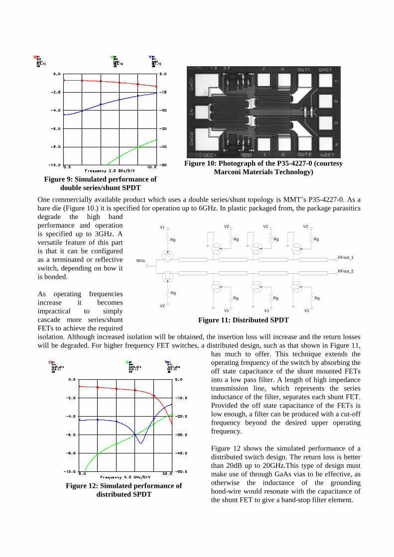
this. The extra switch isolation is provided at the expense of increased insertion loss. The simulated performance of this double series/shunt design is shown in Figure 9. Very good isolation is achieved all the way up to 10GHz, however the input return loss is degrading with frequency and the insertion loss is gradually increasing. As with the single series/shunt design, the use of bond-wires for grounding the shunt FETs will degrade the isolation.
Figure 6: Simulated performance of series/shunt SPDT
Rg
V2
V1
Rg
RFin
V1
Rg
Rg
V2
RFout_1
RFout_2
Rt
Rt
Figure 7: Terminated series/shunt SPDT
Rg
V2
V1
Rg
RFin
V1
Rg
Rg
V2
RFout_1
RFout_2
V1
Rg
Rg
V2
Rg
V2
V1
Rg
Figure 8: Double series/shunt SPDT
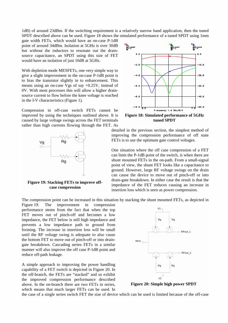
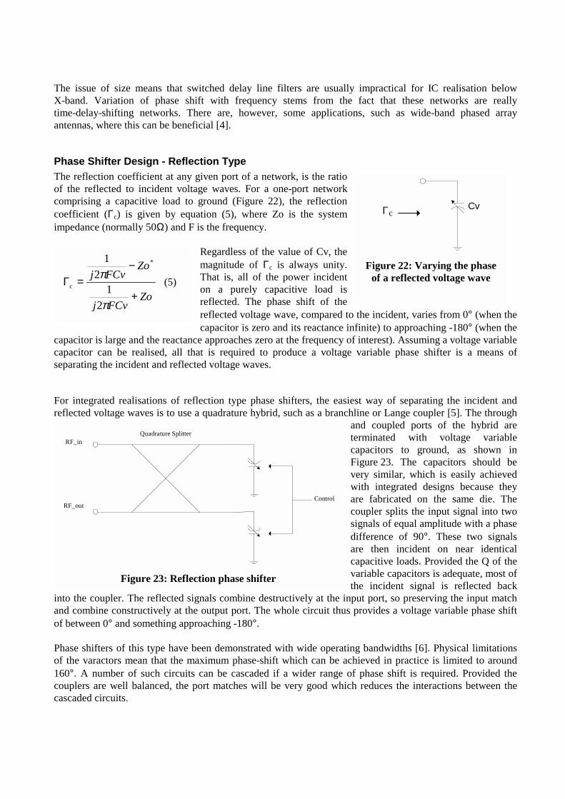
One commercially available product which uses a double series/shunt topology is MMT’s P35-4227-0. As a bare die (Figure 10.) it is specified for operation up to 6GHz. In plastic packaged from, the package parasitics degrade the high band performance and operation is specified up to 3GHz. A versatile feature of this part is that it can be configured as a terminated or reflective switch, depending on how it is bonded. As operating frequencies increase it becomes impractical to simply cascade more series/shunt FETs to achieve the required isolation. Although increased isolation will be obtained, the insertion loss will increase and the return losses will be degraded. For higher frequency FET switches, a distributed design, such as that shown in Figure 11,
has much to offer. This technique extends the operating frequency of the switch by absorbing the off state capacitance of the shunt mounted FETs into a low pass filter. A length of high impedance transmission line, which represents the series inductance of the filter, separates each shunt FET. Provided the off state capacitance of the FETs is low enough, a filter can be produced with a cut-off frequency beyond the desired upper operating frequency. Figure 12 shows the simulated performance of a distributed switch design. The return loss is better than 20dB up to 20GHz.This type of design must make use of through GaAs vias to be effective, as otherwise the inductance of the grounding bond-wire would resonate with the capacitance of the shunt FET to give a band-stop filter element.
Figure 9: Simulated performance of double series/shunt SPDT
Figure 10: Photograph of the P35-4227-0 (courtesy
Marconi Materials Technology)
Rg
V2
V1
Rg
RFin
V1
Rg
Rg
V2
RFout_1
RFout_2
Rg
V2
V1
Rg
Rg
V1
V2
Rg
Figure 11: Distributed SPDT
Figure 12: Simulated performance of
distributed SPDT

Figure 13 shows a photograph of a DC to 20GHz, distributed SPDT, which was fabricated on a 0.5µm gate length process.
Switch Design – Operating Depletion Mode MESFETs Without a Negative Voltage Most commercially available RF and microwave switch ICs utilise depletion mode MESFETs, which means a negative gate-source voltage is required to turn the FET off. Switches can be designed using enhancement mode FETs, which are pinched-off with Vgs=0V and turned on with a small positive Vgs, however the power handling capability tends to be quite poor. It is however straightforward to design switches using depletion mode MESFETs, which do not require a negative supply. The solution is simply to bias the drain and source of the FETs at Vdd, as shown in Figure 14. The FET will now be off for Vg=0V and on for Vg=Vdd. The value of the drain and source bias resistors (Rd) can be made high enough so as not to contribute significantly to the on-case switch loss. Capacitors must be included at the ports of the switch as they are biased and must be DC isolated. The use of capacitors will obviously limit the lower operating frequency of the switch and as they take up a significant amount of die area they tend to be left off commercial switch ICs and included, where necessary, as external discrete components.
Switch Design – Power Compression in Switch FETs Power compression in switching FETs has separate mechanisms in the on-case and the off-case. For the on-case FET it is the peak RF current (Ipk) flowing through the device which causes compression. Figure 15 depicts the RF voltage across a switch FET. Once the RF current swing is high enough (Ipk > Idss) to cause the RF volt-drop across the FET to exceed the knee voltage, the switch starts to compress. Increasing the size of the FET increases the Idss and so its power handling ability.
The Idss of the switch FETs in the simple series FET SPDT (Figure 3) is around 200mA. An RF current of 200mA peak, equates to a power of 1W or +30dBm in a 50Ω system.
Figure 13: Photograph of a distributed SPDT
(courtesy Marconi Materials Technology)
Rg
Vg_2
Vg_1
Rg
RFout_1
RFout_2
RFin
VddVdd
Vdd
Rd
Rd
Rd
Figure 14: Controlling a depletion mode MESFET without a
negative supply

In the off case, the switch FET is high impedance and there is little current flow through it. Compression occurs when the RF voltage swing (VRF ) causes the gate-drain breakdown voltage to be exceeded on the positive half cycle or when it moves the FET out of pinch-off on the negative half cycle. So if the gate-drain breakdown voltage is Vdg_max, the pinch-off voltage is -Vp and the gate is held at -Vg, then one could assume compression would occur once VRF+Vg > Vdg_max or VRF < Vp-Vg. However, at RF frequencies, the impedance of the gate-source capacitance (Cgs) and the gate-drain
capacitance (Cdg) form a potential divider. The gate voltage thus moves dynamically in sympathy with the RF voltage swing on the drain, as depicted in Figure 16.
Vgate
Vg
Vdrain
VRF pk-pk Rds
CdsDrain Source
Rg
Vg
Cdg Cgs
VRF pk-pk2
Figure 16: Dynamic voltages in an off-case switch FET
Cgd and Cgs are equal so Vg is augmented by an RF voltage which is half the magnitude of the voltage on the drain. Thus the voltages at which significant non-linear effects start to occur are given in (1) and (2).
VgVdgVRF −≥ max_2
(1)
VgVpVRF −≤2
(2)
100
200
300
-2 -1 1 2
Ids (mA)
Vds (V)
-200
-300
-100
RF Voltage
Idss
Figure 15: RF voltage-swing in on-case FET

One of these two cases is usually the limiting case, depending on the gate control voltage, Vg. For a typical switch FET process, Vgd_max is around 16V, and Vp is around 2V (pinch-off voltage is -2V). Thus for -5V gate bias, (1) yields VRF > 22V and (2) yields VRF < -6V. Clearly (2) is the limiting case and in a 50Ω system, this equates to an RF power of +25.6dBm. Thus a switch with shunt FETs would have an off-case FET in the on-arm and would start compressing at this sort of level if –5V control were used. This is why switch designs containing shunt mounted FETs can have degraded power compression performance compared to series only designs. It should be noted, however, that series only designs are also effected by this compression mechanism via leakage through the off path. A simple means of improving the compression performance of off-case FETs is to use higher gate control voltages. For example if a -8V gate bias is used, (1) yields VRF > 16V and (2) yields VRF < -12V. Once again (2) is the limiting case and in a 50Ω system, this equates to an RF power of +31.6dBm. Clearly there is an optimum gate bias voltage which will yield the best off-case compression performance for a switch. If Vg is too large, then gate-drain breakdown will occur, as given in equation (1). If Vg is too low then the switch will move out of pinch-off, as given by equation (2). The optimum gate bias voltage (Vg_opt) is easily determined from equations (1) and (2) and is given by equation (3).
2max__ VpVdgoptVg += (3)
So for a process with a 16V gate-drain breakdown voltage and a 2V pinch-off voltage, the optimum gate bias voltage for best off-case switch compression performance would be –9V. The effects of RF voltage augmenting the control voltage applied to the FET’s gate usually increases the power handling capability of switches. However, at lower frequencies, when the resistance of the external bias resistor Rg is low compared to the reactance of Cgs, this effect no longer occurs and the gate bias is held fixed. Cgs depends on the FET gate width and the process used but a value of 0.2pF would not be unrealistic and would give a reactance of 796Ω at 1GHz. If Rg were 4kΩ, then the reactance of Cgs and Cgd would exceed the resistance of Rg at frequencies below around 200MHz. Thus the power handling capability of GaAs switches tends to be reduced for low frequency operation. Obviously this reduction occurs gradually with decreasing frequency. Many suppliers of GaAs switch products specify power compression at 2 frequencies (say 50MHz and 2GHz) to reflect this effect.
Switch Design – Increasing Power Handling The different compression effects in both the on-case and off-case FETs must be considered when evaluating the power handling capability of a switch design. When attempting to increase the power handling capability of a switch different techniques are required to address each state. For on-case switch FETs the simplest way to increase the power handling is to increase the size of the FETs used, which increases the Idss and so the power compression point. The problem which arises, is that this degrades the isolation in the off-case. For narrow band applications, one simple solution to this problem is to put an inductor in parallel with the FET, as depicted in Figure 17. This inductor resonates out the total drain-source capacitance and restores the isolation performance.
By way of example, a 5GHz SPDT is considered. If a simple series FET only design were considered and 20dB isolation was required, then the largest FET which could be used would have a total gate width of 0.26mm. This would have an on-case 1dB compression point (P-
V2
Rg
Rg
RFout_1
RFout_2
RFin
V1
Figure 17: Tuned SPDT
1dB) of around 23dBm. If the switching requirement is a relatively narrow band application, then the tuned SPDT described above can be used. Figure 18 shows the simulated performance of a tuned SPDT using 1mm gate width FETs, which would have an on-case P-1dB point of around 34dBm. Isolation at 5GHz is over 30dB but without the inductors to resonate out the drain-source capacitance, an SPDT using this size of FET would have an isolation of just 10dB at 5GHz. With depletion mode MESFETs, one very simple way to give a slight improvement in the on-case P-1dB point is to bias the transistor slightly in to enhancement. This means using an on-case Vgs of say +0.25V, instead of 0V. With most processes this will allow a higher drain-source current to flow before the knee voltage is reached in the I-V characteristics (Figure 1). Compression in off-case switch FETs cannot be improved by using the techniques outlined above. It is caused by large voltage swings across the FET terminals rather than high currents flowing through the FET. As
detailed in the previous section, the simplest method of improving the compression performance of off state FETs is to use the optimum gate control voltages. One situation where the off case compression of a FET can limit the P-1dB point of the switch, is when there are shunt mounted FETs in the on-path. From a small-signal point of view, the shunt FET looks like a capacitance to ground. However, large RF voltage swings on the drain can cause the device to move out of pinch-off or into drain-gate breakdown. In either case the result is that the impedance of the FET reduces causing an increase in insertion loss which is seen as power compression.
The compression point can be increased in this situation by stacking the shunt mounted FETs, as depicted in Figure 19. The improvement in compression performance stems from the fact that when the top FET moves out of pinch-off and becomes a low impedance, the FET below is still high impedance and prevents a low impedance path to ground from forming. The increase in insertion loss will be small until the RF voltage swing is adequate to also cause the bottom FET to move out of pinch-off or into drain-gate breakdown. Cascading series FETs in a similar manner will also improve the off case P-1dB point and reduce off-path leakage. A simple approach to improving the power handling capability of a FET switch is depicted in Figure 20. In the off-branch, the FETs are “stacked” and so exhibit the improved compression performance described above. In the on-branch there are two FETs in series, which means that much larger FETs can be used. In the case of a single series switch FET the size of device which can be used is limited because of the off-case
Figure 18: Simulated performance of 5GHz tuned SPDT
Rg
RgVg
Figure 19: Stacking FETs to improve off-
case compression
Rg
V1
Rg
RFout_1
RFout_2
RFin
Rg
Rg
V2 Figure 20: Simple high power SPDT

isolation it can provide. However, cascading two devices will essentially double the isolation and so allow larger devices to be used. Using larger FETs means the on-case power compression performance will be improved. This approach, although very simple, offers significant improvements in power handling capability.
Phase Shifter Design Phase shifting circuits allow adjustment of insertion phase. Only techniques which can be used to realise arbitrary phase shifts are considered in this paper. Balun circuits (providing a 0°/180° split) and quadrature hybrids (providing a 0°/90° split), such as Lange couplers, are not explicitly considered as phase shifting elements. There are four practical techniques for realising integrated analogue phase shifters. These are: • Switched delay lines • Reflection type phase shifters • I-Q vector modulators • Switched filter phase shifters
Phase Shifter Design - Switched Delay Line These are the simplest type of phase shifter. A signal passing through a length of transmission line experiences a time delay. This time delay equates to a phase shift of the signal, depending on the physical length of the transmission line, the frequency of the signal and the phase velocity of signals in the transmission line medium. By switching a signal between two pre-determined lengths of transmission line, as depicted in Figure 21, it is therefore possible to realise a specific phase shift at a given frequency.
L1
L2
RF_in RF_out
L = L2 - L1∆
Figure 21: Switched delay line phase shifter
For non-dispersive [2] transmission lines, the phase velocity is equal to the speed of light (c) and the phase shift (φ), in radians, for a length difference ∆L, at a frequency Fo is given by equation (4):
cFoL .2. πφ ∆= (4)
In the case of IC realisations, the transmission lines tend to be microstrip and the phase velocity depends on the electrical permitivity of the substrate, the height of the substrate and the transmission line width [3]. Many modern RF and microwave CAD packages can accurately model the behaviour of microstrip transmission lines, given their physical properties, which makes selecting the required length difference relatively straightforward. The phase shift realised is obviously a digitally controlled step but a number of binary weighted phase shifting “bits” can be cascaded to realise a variable phase shifter covering the desired range. This technique has two main draw-backs: • They become increasingly large with decreasing frequency. • The phase shift varies with frequency
The issue of size means that switched delay line filters are usually impractical for IC realisation below X-band. Variation of phase shift with frequency stems from the fact that these networks are really time-delay-shifting networks. There are, however, some applications, such as wide-band phased array antennas, where this can be beneficial [4].
Phase Shifter Design - Reflection Type The reflection coefficient at any given port of a network, is the ratio of the reflected to incident voltage waves. For a one-port network comprising a capacitive load to ground (Figure 22), the reflection coefficient (Γc) is given by equation (5), where Zo is the system impedance (normally 50Ω) and F is the frequency.
Regardless of the value of Cv, the magnitude of Γc is always unity. That is, all of the power incident on a purely capacitive load is reflected. The phase shift of the reflected voltage wave, compared to the incident, varies from 0° (when the capacitor is zero and its reactance infinite) to approaching -180° (when the
capacitor is large and the reactance approaches zero at the frequency of interest). Assuming a voltage variable capacitor can be realised, all that is required to produce a voltage variable phase shifter is a means of separating the incident and reflected voltage waves.
For integrated realisations of reflection type phase shifters, the easiest way of separating the incident and reflected voltage waves is to use a quadrature hybrid, such as a branchline or Lange coupler [5]. The through
and coupled ports of the hybrid are terminated with voltage variable capacitors to ground, as shown in Figure 23. The capacitors should be very similar, which is easily achieved with integrated designs because they are fabricated on the same die. The coupler splits the input signal into two signals of equal amplitude with a phase difference of 90°. These two signals are then incident on near identical capacitive loads. Provided the Q of the variable capacitors is adequate, most of the incident signal is reflected back
into the coupler. The reflected signals combine destructively at the input port, so preserving the input match and combine constructively at the output port. The whole circuit thus provides a voltage variable phase shift of between 0° and something approaching -180°. Phase shifters of this type have been demonstrated with wide operating bandwidths [6]. Physical limitations of the varactors mean that the maximum phase-shift which can be achieved in practice is limited to around 160°. A number of such circuits can be cascaded if a wider range of phase shift is required. Provided the couplers are well balanced, the port matches will be very good which reduces the interactions between the cascaded circuits.
ΓcCv
Figure 22: Varying the phase
of a reflected voltage wave
ZoFCvj
ZoFCvj
c
+
−=Γ
π
π
21
21 *
(5)
Control
RF_in
RF_out
Quadrature Splitter
Figure 23: Reflection phase shifter

Phase Shifter Design - I-Q Vector Modulators I-Q vector modulators allow arbitrary adjustment of both amplitude and phase [7] and as such can be used as phase shifters. Figure 24 shows a functional block diagram. The input signal is split, equally in amplitude with a 90° phase difference, resulting in an in-phase (I) component and a quadrature (Q) component. A 0° or 180° phase shift is then applied to each signal, allowing the selection of any pair of quadrature vectors. By applying attenuation to one or other of the vectors and in-phase combining them, a signal with any phase across the chosen quadrant can be produced. By adjusting the magnitude of both the I and the Q component, a vector of arbitrary magnitude and phase can be selected. Techniques have been developed which allow the 0°/180° phase shift and the variable attenuation to be realised in a single
functional block which can be conveniently integrated [8]. Single-sideband upconverters [9] can also be used as phase shifters, or more accurately phase modulators. The basic block diagram is shown in Figure 25. This type of modulator is used extensively in wireless communication products to impose complex phase modulation onto an IF or RF carrier [10]. In its simplest form, the carrier frequency will be shifted discretely in 90° steps as the I and Q inputs vary between 00, 01, 10 and 11. The output can thus be depicted by the QPSK constellation diagram. In practice this discrete method is never used and complex low frequency or baseband I and Q signals are used to arbitrarily adjust the amplitude and phase of the carrier signal.
Phase Shifter Design - Switched Filter Phase Shifters The insertion phase through a low pass filter lags the insertion phase through a high pass filter. By switching between two filters, as depicted in Figure 26, a phase shifting element can be produced which has a relatively flat phase shift versus frequency characteristic.
Carrier Frequency
I(t)
Q(t)
Output
0° -90°
Σ
Figure 25: Frequency converting vector modulator
Quadrature SplitterRF_in
RF_out
∠ 0°
∠ -90°
0° / -180°
0° / -180°
I
Q
Figure 24: I-Q vector modulator

Figure 27 shows the simulated insertion loss through a third order high pass Tchebyscheff filter and a third order low pass. Both filters have a cut-off frequency of 5GHz. The insertion phases have a relatively constant phase difference about the cut-off frequency. The insertion phase difference and the insertion loss difference between the two filter responses are plotted in Figure 28. Although the phase difference is
relatively flat with frequency about the cut-off frequency, the amplitude difference variation is significant. This is not surprising since the band-edge slopes of the two filters are rolling in opposite directions with frequency. Simple filter structures such as these are minimum-phase networks, which means their amplitude
and phase responses are inseparably related via the Hilbert Transform [11]. Consequently, if one specifies the amplitude response of such a filter, then the phase response is predetermined. Conversely if the phase
RF_in RF_out
Low Pass
High Pass
Figure 26: Switched filter phase shifter
Figure 27: Insertion loss and phase through HPF and LPF
Figure 28: Insertion loss and phase differences through HPF and LPF
Figure 29: Optimised filters, phase and amplitude differences

response is specified then the amplitude response is predetermined. Since amplitude invariance with phase shift is desirable, and in many applications is a requirement, this presents the designer with a problem. Although it is not possible to design minimum phase networks with prescribed amplitude and phase responses, the simultaneous optimisation of both filters can normally yield satisfactory results. The third order Tchebyscheff filters described above were optimised to give a phase shift of 120° with no amplitude difference across 4 to 6GHz. The results are plotted in Figure 29, across the 4 to 6GHz frequency range the phase shift is within ±1.5° of the desired 120° and the amplitude difference between states is less than ±0.05dB.
This method can be used to design phase shifting elements of arbitrary value. Basically, the higher the value of phase shift required, the higher the order of filters which will yield the optimum result. This type of phase shifter has the draw back that it incurs the insertion loss of two SPDTs. For multi-bit designs this can soon become substantial. One technique, which can be used to reduce this loss, is to use a reconfigurable switched filter such as that shown in Figure 30. This technique is particularly well suited to realising lower value phase shifting bits. With both switches open, the circuit is a series inductor, a low pass element. With both switches closed the circuit is an inductance to ground, a high pass element.
Figure 31 shows the simulated performance of a reconfigurable phase shifter, optimised to give 22.5° phase shift across the 4 to 6GHz frequency range. The simulated phase shift is within ±0.4° of the desired 22.5° and the amplitude difference between states is less than ±0.15dB. Accuracy of phase-shift can be traded for improved amplitude balance and return loss. Multi-bit switched filter phase shifters can be used to realise digitally controlled phase shifters covering 360° [12]. Binary weighted bits are commonly used thus a 6-bit 360° phase shifter, such as that shown in Figure 32, would have bits of 180°, 90°, 45°, 22.5°, 11.25° and 5.625°.
RF_in RF_out
Figure 30: A reconfigurable switched filter
phase shifter
Figure 31: Simulated performance of a 22.5°°°° reconfigurable phase shifter
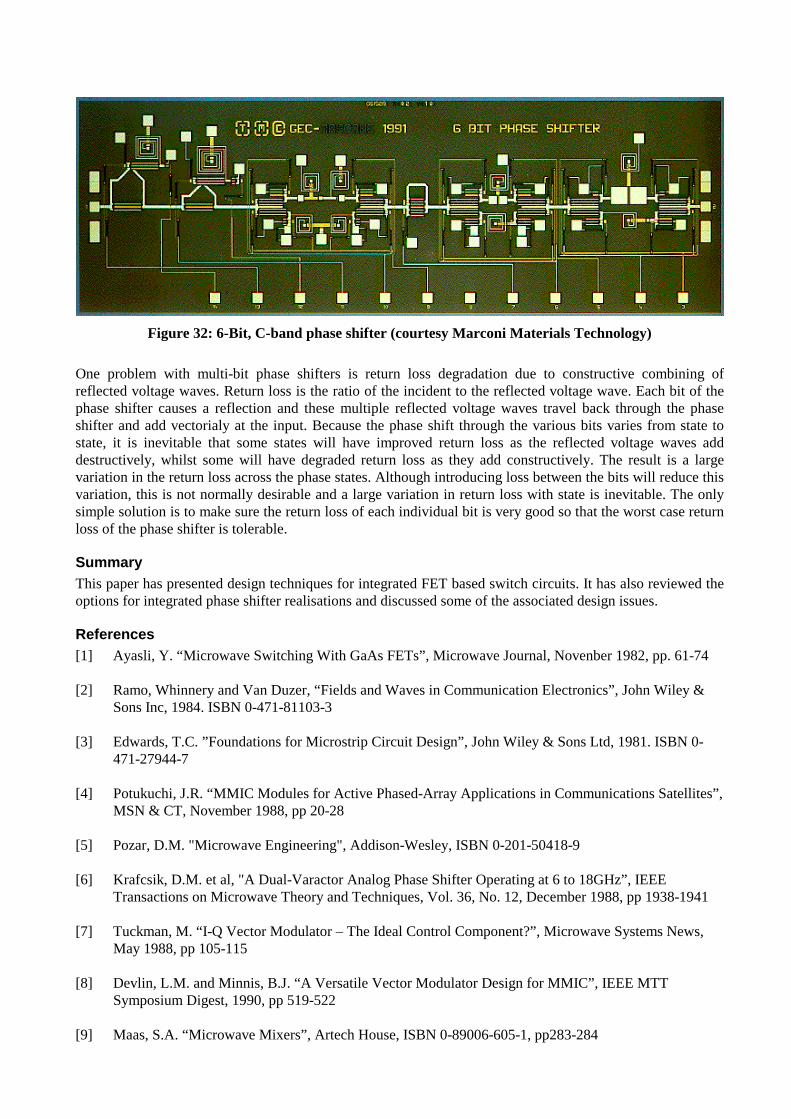
Figure 32: 6-Bit, C-band phase shifter (courtesy Marconi Materials Technology)
One problem with multi-bit phase shifters is return loss degradation due to constructive combining of reflected voltage waves. Return loss is the ratio of the incident to the reflected voltage wave. Each bit of the phase shifter causes a reflection and these multiple reflected voltage waves travel back through the phase shifter and add vectorialy at the input. Because the phase shift through the various bits varies from state to state, it is inevitable that some states will have improved return loss as the reflected voltage waves add destructively, whilst some will have degraded return loss as they add constructively. The result is a large variation in the return loss across the phase states. Although introducing loss between the bits will reduce this variation, this is not normally desirable and a large variation in return loss with state is inevitable. The only simple solution is to make sure the return loss of each individual bit is very good so that the worst case return loss of the phase shifter is tolerable.
Summary This paper has presented design techniques for integrated FET based switch circuits. It has also reviewed the options for integrated phase shifter realisations and discussed some of the associated design issues.
References [1] Ayasli, Y. “Microwave Switching With GaAs FETs”, Microwave Journal, Novenber 1982, pp. 61-74 [2] Ramo, Whinnery and Van Duzer, “Fields and Waves in Communication Electronics”, John Wiley &
Sons Inc, 1984. ISBN 0-471-81103-3 [3] Edwards, T.C. ”Foundations for Microstrip Circuit Design”, John Wiley & Sons Ltd, 1981. ISBN 0-
471-27944-7 [4] Potukuchi, J.R. “MMIC Modules for Active Phased-Array Applications in Communications Satellites”,
MSN & CT, November 1988, pp 20-28 [5] Pozar, D.M. "Microwave Engineering", Addison-Wesley, ISBN 0-201-50418-9 [6] Krafcsik, D.M. et al, "A Dual-Varactor Analog Phase Shifter Operating at 6 to 18GHz”, IEEE
Transactions on Microwave Theory and Techniques, Vol. 36, No. 12, December 1988, pp 1938-1941 [7] Tuckman, M. “I-Q Vector Modulator – The Ideal Control Component?”, Microwave Systems News,
May 1988, pp 105-115 [8] Devlin, L.M. and Minnis, B.J. “A Versatile Vector Modulator Design for MMIC”, IEEE MTT
Symposium Digest, 1990, pp 519-522
[9] Maas, S.A. “Microwave Mixers”, Artech House, ISBN 0-89006-605-1, pp283-284

[10] Norton, D.E. et al, “I and Q Modulators for Cellular Communications Systems”, Microwave Journal,
October 1991, pp 63-80
[11] Rhea, R.W. “HF Filter Design and Computer Simulation”, Noble Publishing, Atlanta, 1994, ISBN: 1-884932-25-8
[12] Devlin, L.M. “Digitally Controlled, 6 Bit, MMIC Phase Shifter for SAR Applications”, Proceedings of
the 22nd European Microwave Conference, 1992 pp 225-230


![MWP phase shifters integrated in PbS-SU8 waveguides · PDF fileMWP phase shifters integrated in PbS-SU8 waveguides ... Marpaung, C. Roeloffzen, R. Heideman, ... [16], SOA based](https://img.pdfslide.us/doc/110x75/5a869ff07f8b9a882e8d11ac/mwp-phase-shifters-integrated-in-pbs-su8-waveguides-phase-shifters-integrated-in.jpg)

![A 10 bits three channels 0.35 um SiGe phase shifter · 2016-04-05 · distributed-type phase shifters (DTPSs) [8]. The phase shifters which use a vector sum of two or more orthogonal-phased](https://img.pdfslide.us/doc/110x75/5fa2ca0e17d7536493327223/a-10-bits-three-channels-035-um-sige-phase-shifter-2016-04-05-distributed-type.jpg)
![Liquid Crystal Based Dielectric Waveguide Phase Shifters ... · tems (MEMS) are available as possible solutions for DW phase shifters. In [5] and [6] high impedance surfaces (HIS)](https://img.pdfslide.us/doc/110x75/5f6580af6a466a36f634975b/liquid-crystal-based-dielectric-waveguide-phase-shifters-tems-mems-are-available.jpg)