Embed Size (px)
Citation preview
ANALYSIS AND DESIGN OF W-BAND PHASE SHIFTERS
BY
IOANNIS SARKAS
A THESIS SUBMITTED IN CONFORMITY WITH THE REQUIREMENTS
FOR THE DEGREE OF MASTER OF APPLIED SCIENCE
GRADUATE DEPARTMENT OF ELECTRICAL AND COMPUTER ENGINEERING
UNIVERSITY OF TORONTO
c© IOANNIS SARKAS, 2010


ANALYSIS AND DESIGN OF W-BAND PHASE SHIFTERS
Ioannis SarkasMaster of Applied Science, 2010
Graduate Department of Electrical and Computer EngineeringUniversity of Toronto
Abstract
This thesis describes 80−94GHz and 70−77GHz interpolating phase shifters and the cor-
responding transmitter and receiver ICs, fabricated in 65-nm CMOS and SiGe BiCMOS tech-
nologies, respectively. Lumped inductors and transformers are employed to realize small-form
factor 90◦ hybrids as needed in high density phased arrays. The CMOS transmitter exhibits
absolute phase and amplitude errors of 4◦ and 4dB, respectively, at 90GHz, when the phase
is varied from 0◦ to 360◦ in steps of 22.5◦. The absolute phase error in the SiGe BiCMOS
receiver is less than 5◦, with a maximum gain imbalance below 3dB at 74GHz. The peak gain
and power consumption are 3.8dB and 142mW from 1.2V supply for the CMOS transmitter,
and 17dB and 128mW from 1.5V and 2.5V supplies for the SiGe BiCMOS receiver.
iii

iv

Acknowledgements
I would like to sincerely thank Professor Sorin P. Voinigescu for his invaluable advice and
guidance. It is my honour to have him as my advisor and colleague. I would also like to
acknowledge my examination committee Professors Roman Genov, Ali Sheikholeslami and
Frank Kschischang.
I am also grateful to my colleagues from BA4182 who have assisted me during the tenure
of my Master’s program. Particularly, I would like to thank Dr. Sean Nicolson for his invalu-
able advice, Kenneth Yau who taught me everything I know about measurements and Andreea
Balteanu for her on going moral support.
This thesis would not have been possible without the never ending support of my parents,
my brother and all my friends in Toronto and Greece.
This project was supported by the Natural Science and Engineering Council of Canada
(NSERC) and STMicroelectronics.
v

vi
Table of Contents
Abstract iii
Acknowledgements v
List of Tables ix
List of Figures xii
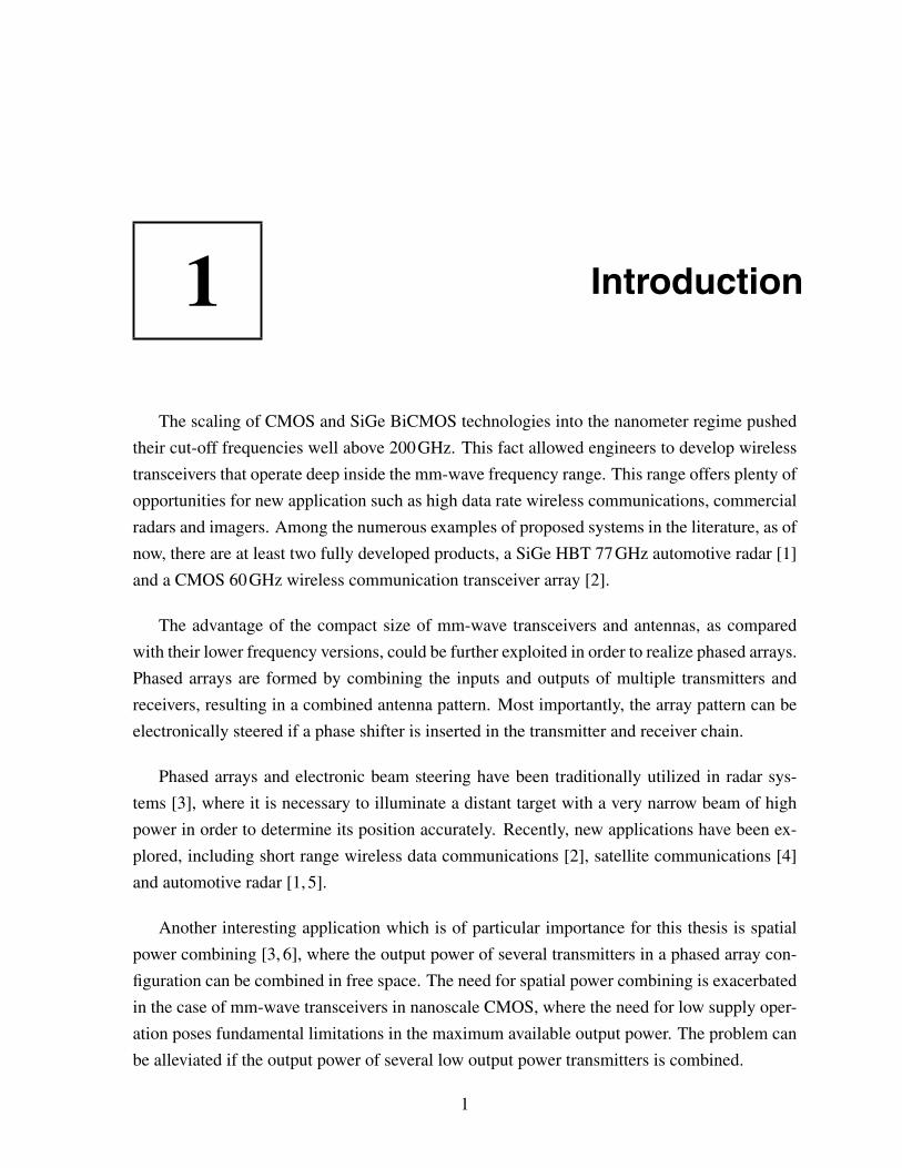
1 Introduction 1
1.1 Phased Arrays . . . . . . . . . . . . . . . . . . . . . . . . . . . . . . . . . . . 2
1.2 Objective of Thesis . . . . . . . . . . . . . . . . . . . . . . . . . . . . . . . . 4
1.3 Technology Overview and mm-wave Circuit Design Aspects . . . . . . . . . . 5
2 Phase Shifter Architectures 7
2.1 Introduction . . . . . . . . . . . . . . . . . . . . . . . . . . . . . . . . . . . . 7
2.2 Definition and Categorization . . . . . . . . . . . . . . . . . . . . . . . . . . . 7
2.3 Digital Phase Shifters . . . . . . . . . . . . . . . . . . . . . . . . . . . . . . . 9
2.3.1 Switched Line Phase Shifter . . . . . . . . . . . . . . . . . . . . . . . 9
2.3.2 Reflection Type Phase Shifter . . . . . . . . . . . . . . . . . . . . . . 10
2.3.3 Loaded Line Phase Shifter . . . . . . . . . . . . . . . . . . . . . . . . 11
2.3.4 High Pass - Low Pass Type Phase Shifter . . . . . . . . . . . . . . . . 11
2.3.5 Multibit Digital Phase shifters . . . . . . . . . . . . . . . . . . . . . . 14
2.4 Continuous Phase Shifters . . . . . . . . . . . . . . . . . . . . . . . . . . . . 15
2.4.1 Analog Reflection Type Phase Shifter . . . . . . . . . . . . . . . . . . 15
2.4.2 Tunable Filter Type Phase Shifter . . . . . . . . . . . . . . . . . . . . 16
2.4.3 Periodically Loaded Transmission Line Phase Shifter . . . . . . . . . . 17
2.4.4 Dual Gate FET Type Phase Shifter . . . . . . . . . . . . . . . . . . . . 19
vii

viii Table of Contents
2.4.5 Phase Interpolation Phase Shifter . . . . . . . . . . . . . . . . . . . . 20
2.5 Phase Shifter Architecture Summary . . . . . . . . . . . . . . . . . . . . . . . 23
2.6 Other Applications of Phase Shifters . . . . . . . . . . . . . . . . . . . . . . . 23
2.6.1 I-Q Calibration . . . . . . . . . . . . . . . . . . . . . . . . . . . . . . 23
2.6.2 Frequency Translators - Modulators . . . . . . . . . . . . . . . . . . . 24
2.7 Conclusion . . . . . . . . . . . . . . . . . . . . . . . . . . . . . . . . . . . . 25
3 Analysis and Design Of Phase Interpolation Phase Shifters 27
3.1 Choice of Phase Shifter Topology . . . . . . . . . . . . . . . . . . . . . . . . 27
3.2 System Analysis of the Phase Interpolation Phase Shifter . . . . . . . . . . . . 28
3.3 Error Model for the Interpolation Phase Shifter . . . . . . . . . . . . . . . . . 29
3.4 I-Q Splitting . . . . . . . . . . . . . . . . . . . . . . . . . . . . . . . . . . . . 35
3.4.1 All-Pass Polyphase filter . . . . . . . . . . . . . . . . . . . . . . . . . 35
3.4.2 Lumped Quadrature Hybrid . . . . . . . . . . . . . . . . . . . . . . . 36
3.5 Variable Gain Amplifiers . . . . . . . . . . . . . . . . . . . . . . . . . . . . . 38
3.5.1 65-nm CMOS, 94 GHz Variable Gain Amplifier . . . . . . . . . . . . . 38
3.5.2 130-nm SiGe BiCMOS, 77 GHz Variable Gain Amplifier . . . . . . . . 40
3.6 Phase Rotators . . . . . . . . . . . . . . . . . . . . . . . . . . . . . . . . . . 43
3.6.1 65-nm CMOS, 94 GHz Phase Rotator . . . . . . . . . . . . . . . . . . 43
3.6.2 130-nm SiGe BiCMOS, 77 GHz Phase Rotator . . . . . . . . . . . . . 45
3.7 130-nm SiGe BiCMOS, 77 GHz Receiver with Phase Shifting . . . . . . . . . 48
3.8 65-nm CMOS, 94 GHz Transmitter with Phase Shifting . . . . . . . . . . . . . 51
4 Characterization 55
4.1 77 GHz Receiver with Phase Shifting . . . . . . . . . . . . . . . . . . . . . . 55
4.2 94 GHz Transmitter with Phase Shifting . . . . . . . . . . . . . . . . . . . . . 59
4.3 Comparison with Relevant Work . . . . . . . . . . . . . . . . . . . . . . . . . 62
5 Conclusion 63
5.1 Contributions . . . . . . . . . . . . . . . . . . . . . . . . . . . . . . . . . . . 63
5.2 Future Work . . . . . . . . . . . . . . . . . . . . . . . . . . . . . . . . . . . . 64
5.3 Publication . . . . . . . . . . . . . . . . . . . . . . . . . . . . . . . . . . . . 65

List of Tables
3.1 RI/Q for different phase shifts and phase arrangements. . . . . . . . . . . . . . 30
3.2 AI and AQ for different phase shifts and arrangements. . . . . . . . . . . . . . . 30
3.3 Phase and amplitude errors of the phase shifter. . . . . . . . . . . . . . . . . . 33
4.1 Measured versus simulated performance of the 77GHz receiver. . . . . . . . . 59
4.2 Measured versus simulated performance of the 94GHz transmitter. . . . . . . . 62
4.3 Comparison of different phase shifters. . . . . . . . . . . . . . . . . . . . . . . 62
ix

x List of Tables

List of Figures
1.1 One dimensional arrays. . . . . . . . . . . . . . . . . . . . . . . . . . . . . . 2
1.2 One and two dimensional array directivity patterns. . . . . . . . . . . . . . . . 3
1.3 Transmitter and receiver arrays . . . . . . . . . . . . . . . . . . . . . . . . . . 4
2.1 Phase versus frequency characteristics of phase shifters. . . . . . . . . . . . . . 8
2.2 Switched line phase shifter. . . . . . . . . . . . . . . . . . . . . . . . . . . . . 9
2.3 Reflection type phase shifters. . . . . . . . . . . . . . . . . . . . . . . . . . . 10
2.4 Loaded line phase shifter. . . . . . . . . . . . . . . . . . . . . . . . . . . . . . 11
2.5 Π and T networks. . . . . . . . . . . . . . . . . . . . . . . . . . . . . . . . . 13
2.6 Switched – bypass phase shifters. . . . . . . . . . . . . . . . . . . . . . . . . . 13
2.7 Switched high-pass – low-pass phase shifters. . . . . . . . . . . . . . . . . . . 14
2.8 Cascade of four single phase shift bits resulting in a phase shifter with 16 states. 14
2.9 Distributed switch phase shifter. . . . . . . . . . . . . . . . . . . . . . . . . . 15
2.10 Reflection type phase shifter with lumped loads. . . . . . . . . . . . . . . . . . 16
2.11 Tunable low-pass T network. . . . . . . . . . . . . . . . . . . . . . . . . . . . 16
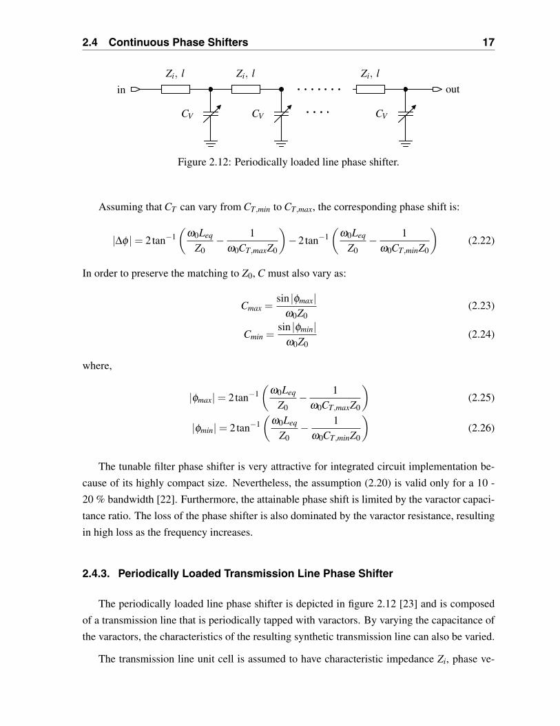
2.12 Periodically loaded line phase shifter. . . . . . . . . . . . . . . . . . . . . . . 17
2.13 Dual gate phase shifter. . . . . . . . . . . . . . . . . . . . . . . . . . . . . . . 19
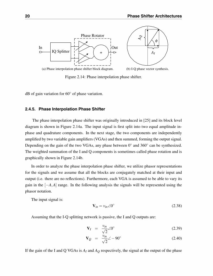
2.14 Phase interpolation phase shifter. . . . . . . . . . . . . . . . . . . . . . . . . . 20
2.15 Quadrant selection according to the gain sign. . . . . . . . . . . . . . . . . . . 22
2.16 I-Q receiver architectures. . . . . . . . . . . . . . . . . . . . . . . . . . . . . . 24
2.17 Frequency translator. . . . . . . . . . . . . . . . . . . . . . . . . . . . . . . . 25
3.1 Interpolation phase shifter utilizing differential signals. . . . . . . . . . . . . . 28
3.2 Phase shifter signal constellation under various errors. . . . . . . . . . . . . . . 32
3.3 Monte Carlo error simulation of phase shifter signal constellation. . . . . . . . 34
3.4 All-Pass polyphase filter. . . . . . . . . . . . . . . . . . . . . . . . . . . . . . 35
3.5 All-Pass polyphase filter simulation results. . . . . . . . . . . . . . . . . . . . 36
xi

xii List of Figures
3.6 Two versions of the lumped quadrature hybrid. . . . . . . . . . . . . . . . . . 37
3.7 Lumped quadrature hybrid simulation results. . . . . . . . . . . . . . . . . . . 38
3.8 65-nm CMOS, 94 GHz CMOS variable gain amplifier. . . . . . . . . . . . . . 39
3.9 130-nm SiGe BiCMOS, 77 GHz variable gain amplifier. . . . . . . . . . . . . 41
3.10 Gilbert-cell quad admittance analysis model. . . . . . . . . . . . . . . . . . . . 42
3.11 65-nm CMOS, 94 GHz CMOS phase rotator. . . . . . . . . . . . . . . . . . . 44
3.12 Transfer characteristics versus gain control for the SiGe variable gain amplifier. 45
3.13 S21 and IP1dB variations as a function of small signal gain for the CMOS vari-
able gain amplifier. . . . . . . . . . . . . . . . . . . . . . . . . . . . . . . . . 46
3.14 130-nm SiGe BiCMOS, 77 GHz phase rotator. . . . . . . . . . . . . . . . . . . 46
3.15 Transfer Characteristics versus gain control for the SiGe Variable Gain Amplifier. 47
3.16 S21 and IP1dB variations as a function of small signal gain for the SiGe variable
gain amplifier. . . . . . . . . . . . . . . . . . . . . . . . . . . . . . . . . . . . 47
3.17 SiGe BiCMOS 77GHz receiver. . . . . . . . . . . . . . . . . . . . . . . . . . 48
3.18 SiGe BiCMOS 77GHz low noise amplifier. . . . . . . . . . . . . . . . . . . . 49
3.19 SiGe 77-GHz receiver simulations. . . . . . . . . . . . . . . . . . . . . . . . . 50
3.20 CMOS 94GHz transmitter. . . . . . . . . . . . . . . . . . . . . . . . . . . . . 51
3.21 Input and differential buffers utilized in the transmitter. . . . . . . . . . . . . . 52
3.22 CMOS 94GHz power amplifier. . . . . . . . . . . . . . . . . . . . . . . . . . 53
3.23 CMOS 94-GHz transmitter simulations. . . . . . . . . . . . . . . . . . . . . . 54
4.1 SiGe BiCMOS 77GHz receiver die photo. . . . . . . . . . . . . . . . . . . . . 56
4.2 77GHz receiver measurement setups. . . . . . . . . . . . . . . . . . . . . . . 57
4.3 77GHz receiver measurement results. . . . . . . . . . . . . . . . . . . . . . . 58
4.4 77GHz receiver measured noise figure. . . . . . . . . . . . . . . . . . . . . . 58
4.5 65nm CMOS 94GHz transmitter die photo. . . . . . . . . . . . . . . . . . . . 60
4.6 94GHz transmitter measurement results. . . . . . . . . . . . . . . . . . . . . . 61
5.1 Errors in phased array systems. . . . . . . . . . . . . . . . . . . . . . . . . . . 64
1 Introduction
The scaling of CMOS and SiGe BiCMOS technologies into the nanometer regime pushed
their cut-off frequencies well above 200GHz. This fact allowed engineers to develop wireless
transceivers that operate deep inside the mm-wave frequency range. This range offers plenty of
opportunities for new application such as high data rate wireless communications, commercial
radars and imagers. Among the numerous examples of proposed systems in the literature, as of
now, there are at least two fully developed products, a SiGe HBT 77GHz automotive radar [1]
and a CMOS 60GHz wireless communication transceiver array [2].
The advantage of the compact size of mm-wave transceivers and antennas, as compared
with their lower frequency versions, could be further exploited in order to realize phased arrays.
Phased arrays are formed by combining the inputs and outputs of multiple transmitters and
receivers, resulting in a combined antenna pattern. Most importantly, the array pattern can be
electronically steered if a phase shifter is inserted in the transmitter and receiver chain.
Phased arrays and electronic beam steering have been traditionally utilized in radar sys-
tems [3], where it is necessary to illuminate a distant target with a very narrow beam of high
power in order to determine its position accurately. Recently, new applications have been ex-
plored, including short range wireless data communications [2], satellite communications [4]
and automotive radar [1, 5].
Another interesting application which is of particular importance for this thesis is spatial
power combining [3, 6], where the output power of several transmitters in a phased array con-
figuration can be combined in free space. The need for spatial power combining is exacerbated
in the case of mm-wave transceivers in nanoscale CMOS, where the need for low supply oper-
ation poses fundamental limitations in the maximum available output power. The problem can
be alleviated if the output power of several low output power transmitters is combined.
1

2 Introduction
In-Phase Power Combiner
φφφφ
(a) Phased array.
In-Phase Power Combiner
ττττ
(b) Time delay array.
Figure 1.1: One dimensional arrays.
1.1. Phased Arrays
Consider the system of Figure 1.1a. The signals from the antennas can be combined
by appropriately spacing them and arranging the corresponding phase shifts. The resulting
antenna can have various properties, depending on the system; most importantly, the main lobe
of the antenna can be electronically steered in a desired direction. The same idea applies to
both receiving and transmitting arrays.
A simple array case is when the phase shifts in the one dimensional, linear, N-element
array of Figure 1.1a are progressively increased as: 0, Δφ , 2Δφ , . . . NΔφ . Assuming that
the elements are ideal isotropic antennas, the rotationally-symmetric radiation pattern of the
resulting system is given by [7]:
F =N
∑n=1
e j(n−1)ψ � sin(N2 ψ)
ψ2
(1.1)
ψ = kd cosθ +Δφ
where k = 2π/λ , d is the antenna spacing and θ is the angle perpendicular to the array axis.
The radiation pattern maximum occurs at:
θm = cos−1(
λΔφ2πd
)(1.2)
Figure 1.2a illustrates the antenna array directivity patterns when Δφ = 0◦,45◦,90◦. The
patterns correspond to a linear array of N = 15 isotropic radiators, placed on the z-axis, where
the inter-element spacing is d = λ/4. As seen in the figure, the radiation pattern can be changed
based on the applied phase shift. As a result, it is possible to receive or transmit from a desired
direction that is chosen by setting the appropriate phase shift to the phase shifters. The same
principle with slightly more complicated mathematics [7] applies in the case of a two dimen-

1.1 Phased Arrays 3
Δφ = 45◦
Δφ = 0◦
Δφ = 90◦
z
x y
(a) 1-D Array directivity patterns. The linear array lieson the z-axis.
Δφxy = 45◦
Δφxy = 0◦
Δφxy =−45◦
z
x y
(b) 2-D Array directivity patterns. The array lieson the xy-plane.
Figure 1.2: One and two dimensional array directivity patterns.
sional array where the isotropically radiating elements are placed on a rectangular grid on the
x-y plane. The resulting antenna directivity patterns are shown in 1.2b. In the rectangular array
case, it is possible to fully steer the beam in any direction in one of the two hemispheres of
the 3-D space. It should be noted that there are other amplitude and phase shift options for the
array elements than can yield other array patterns [6, 7].
There are two fundamental limitations in the phased array implementation of figure 1.1a.
First, the constant-phase phase shifters presented in the previous section can, at most, generate
a phase shift between 0◦ and 360◦. However, the most common array topologies require a
progressive phase shift between the elements of the form 0, Δφ , 2Δφ , . . . NΔφ . As a result,
the phase shift of the elements that exceed 360◦ must be truncated by k · 360◦ in order to be
brought back into the 0◦ −360◦ range. Second, as can be seen in equation (1.2), the radiation
pattern maximum depends on the wavelength λ when d is constant. Therefore, for a constant
Δφ over frequency, the array pattern will not be constant over the bandwidth of operation.
These two limitations result in an overall constraint over the bandwidth of operation of the
array. Moreover, this bandwidth constraint gets more severe as the number of elements in the
array increases [4].
In case the bandwidth limitation needs to be avoided, or in case the number of elements is
very large and the bandwidth constraint cannot be met, the architecture of Figure 1.1b could
be considered. If the constant-phase phase shifters are replaced with true time delay phase
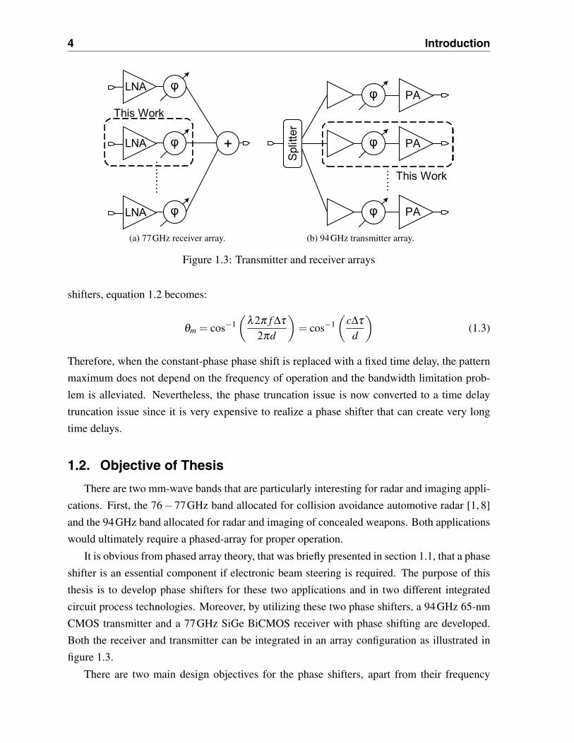
4 Introduction
φLNA
φLNA
φLNA
+
This Work
(a) 77GHz receiver array.
Spl
itter
φ PA
φ PA
φ PA
This Work
(b) 94GHz transmitter array.
Figure 1.3: Transmitter and receiver arrays
shifters, equation 1.2 becomes:
θm = cos−1(
λ2π f Δτ2πd
)= cos−1
(cΔτ
d
)(1.3)
Therefore, when the constant-phase phase shift is replaced with a fixed time delay, the pattern
maximum does not depend on the frequency of operation and the bandwidth limitation prob-
lem is alleviated. Nevertheless, the phase truncation issue is now converted to a time delay
truncation issue since it is very expensive to realize a phase shifter that can create very long
time delays.
1.2. Objective of Thesis
There are two mm-wave bands that are particularly interesting for radar and imaging appli-
cations. First, the 76− 77GHz band allocated for collision avoidance automotive radar [1, 8]
and the 94GHz band allocated for radar and imaging of concealed weapons. Both applications
would ultimately require a phased-array for proper operation.
It is obvious from phased array theory, that was briefly presented in section 1.1, that a phase
shifter is an essential component if electronic beam steering is required. The purpose of this
thesis is to develop phase shifters for these two applications and in two different integrated
circuit process technologies. Moreover, by utilizing these two phase shifters, a 94GHz 65-nm
CMOS transmitter and a 77GHz SiGe BiCMOS receiver with phase shifting are developed.
Both the receiver and transmitter can be integrated in an array configuration as illustrated in
figure 1.3.
There are two main design objectives for the phase shifters, apart from their frequency

1.3 Technology Overview and mm-wave Circuit Design Aspects 5
of operation. First, they need to be able to generate phase shifts from 0◦ to 360◦ so that the
resulting 2D array will be able to scan a whole hemisphere. Second, at least sixteen, equidistant
steps of 22.5◦ are required in order to steer the beam with high angular resolution while the
array elements are reasonably spaced (equation 1.2).
1.3. Technology Overview and mm-wave Circuit Design Aspects
Two technologies were utilized for the circuits developed in this work, both provided by
STMicroelectronics. A 130-nm SiGe BiCMOS [9] process and a 65-nm CMOS process.
STMicroelectronics’ 130-nm SiGe BiCMOS (BICMOS9MW) is a dedicated, all-copper,
millimeter-wave process. It features two thick metal metallization layers, intended for low-loss
transmission lines and inductors, and high quality factor Alucap MIM (Metal-Insulator-Metal)
capacitors. The HBT transistors achieve fT of 240GHz and fMAX 270 GHz. The current
density that yields the maximum power gain at each frequency is 1.4mA per micron of emitter
length. The measured HBT Maximum Available Gain (MAG) at 77GHz is above 9dB. The
130-nm n-MOSFET devices feature fT / fMAX of 85/95 GHz when biased at 0.3 mA per micron
of gate width, and the VDS voltage is 1.2V
STMicroelectronics’ standard 65-nm CMOS process features 7-layer Cu back-end, as well
as MIM capacitors. Both LP and GP transistors are available on the same die. However,
because GP transistors exhibit 20-30% higher gm and fT , and lower VT , they were used exclu-
sively in all circuits. The General Purpose (GP) NMOS transistors exhibit peak fT of 180GHz
when biased at 0.3mA to 0.35mA per gate width, with VDS = 0.7V, while their MAG is 8dB
at 94GHz.
In the circuits presented in this thesis, all transistors are biased at their peak fMAX current
densities in order to obtain as much gain as possible out of them [10, 11]. The only exception
is the first two 77GHz low noise amplifier stages that are biased at slightly lower current for
optimum noise figure. In all NMOS transistors, the finger width is 1 μm while the drawn
emitter width of all HBTs is 0.13 μm. In addition, all passive components are realized using
lumped inductors and transformers as described in [11, 12].

6 Introduction

2 Phase Shifter Architectures
2.1. Introduction
This chapter reviews the theory of high-frequency phase shifters. It starts with a formal
definition of the phase shifter as a circuit building block. Then, the different microwave phase
shifter topologies that can be realized in standard integrated circuit form are presented and ana-
lyzed. An attempt is made to present the main advantages and disadvantages of each topology.
Phase shifter topologies involving ferrites, Surface Acoustic Wave devices, exotic dielectrics
and optics will not be analyzed in this work.
Almost all topologies were first proposed and analyzed between 1955 – 1975. During this
period the Cold War was at its peak and there was a demand of accurate, long range (i.e. high
power) radars. This demand drove the microwave engineers to innovate, notably in digitally
controlled phase shifters, utilizing mainly PIN diodes [13–16]. The interest in microwave
and mm-wave phase shifters was revived recently due to the application of phased arrays in
commercial radars (i.e. 24GHz and 77GHz automotive radars), radios (60GHz radios) as well
as low cost military (Q, X, K, Ka and Ku band) radars.
2.2. Definition and Categorization
Throughout this work, an ideal phase shifter will be defined through its scattering parameter
matrix as:
S =
[0 A e− jφ
A e− jφ 0
](2.1)
where A is the gain of the phase shifter and φ is the applied phase shift. The purpose of the
phase shifter is to change the phase of the signal applied at its input in a known and well defined
manner. If φ is constant then the phase shifter is a Fixed Phase Shifter [17]. If φ can be varied
though an external control signal then the phase shifter is a Tunable Phase Shifter. Ideally,
7

8 Phase Shifter Architectures
Frequency (Hz)
Phas
e(D
egre
es)
(a) Phase versus frequency characteristics of a con-stant phase type shift shifter.
Frequency (Hz)
Phas
e(D
egre
es)
(b) Phase versus frequency characteristics of a con-stant time delay shifter.
Figure 2.1: Phase versus frequency characteristics of phase shifters.
the gain of a tunable phase shifter remains constant when the phase shift varies. Nevertheless,
based on the application, small variations of the gain can be tolerated. It should be noted that
the generic definition (2.1) applies only to reciprocal phase shifters. There are certain types of
non-reciprocal shifters that can be represented by a slight modification of (2.1).
Based on how the phase shift can be controlled, two major categories can be distinguished:
• Continuous phase shifters. These shifters can vary the phase of the input signal in a cer-
tain range [φmin,φmax] in a continuous way. I.e. every phase within the range [φmin,φmax]
can be obtained when the control voltages are set appropriately.
• Digital phase shifters. These shifters can only apply certain phase shift values φ1,φ2, · · · ,φn
to the input signal. Usually, the phase shift is controlled by setting the corresponding
control bits.
There are two other major phase shifter categories that are not immediately apparent from
equation (2.1). The equation can be modified so that it expresses the scattering parameter
matrix over frequency:
S(ω) =
[0 A(ω) e− jφ(ω)
A(ω) e− jφ(ω) 0
](2.2)
As a result, based on the frequency variation of the phase shift, the following two categories
could be specified:
• Constant phase type phase shifters. These shifters apply a constant phase shift over
frequency to the input signal, i.e. φ(ω) = φ0 (Figure 2.1a).

2.3 Digital Phase Shifters 9
l0
l0 + l
in out
ctrl
Figure 2.2: Switched line phase shifter.
• Constant time delay type phase shifters (or True Time Delay (TTD) phase shifters).
These phase shifters apply a constant time delay to the input signal: φ(ω) = ω · Δt.
I.e, the phase varied linearly with respect to frequency (Figure 2.1b).
In both categories, the gain is required to remain constant over frequency: A(ω) = A0. Since
φ = ωΔt, the two phase shifter types are equivalent over a narrow bandwidth. As presented
in the introduction, constant time delay phase shifting is highly desirable for phased arrays,
which constitutes the major application of phase shifters.
2.3. Digital Phase Shifters
This section discusses and compares different digital phase shifter architectures. First the
various methods of creating a phase shift bit are presented. Then, two ways of creating a
multi-bit phase shifter will be shown.
2.3.1. Switched Line Phase Shifter
In the Switched Line Phase Shifter, it is possible to switch between two different time
delays, realized with transmission lines, as illustrated in Figure 2.2. The time delay of a trans-
mission line of length l0 is τD = 2πl0vp
, where vp is the phase velocity of the guided wave. As a
result, the time delay of the two states is given by
Δτ =2πlvp
(2.3)
where l is the length difference between the two transmission lines.
The major advantage of the switched line phase shifter is that it can realize variable time
10 Phase Shifter Architectures
l/2
in
out
ctrl
(a) Hybrid coupler based reflection type phase shifter.
l/2
in
outctrl
(b) Circulator based reflection type phase shifter.
Figure 2.3: Reflection type phase shifters.
delay, rendering it ideal for wideband array applications. However there are three disadvan-
tages associated it. First, two single-pole double-throw switches are required and as a result, an
advanced CMOS technology is needed to realize this phase shifter at high frequencies with low
switch insertion loss. Second, the two lines that realize the time delays have unequal lengths
and different attenuations. This implies that the two time delay states will have different attenu-
ations, resulting in amplitude imbalance between the two states. Third, in order to realize large
time delays, long line lengths are required resulting in impractical size for integrated circuit
realization for most frequency ranges and in increased loss for larger time delays.
2.3.2. Reflection Type Phase Shifter
A reflection type phase shifter takes advantage of the directional properties of a 3-dB hybrid
coupler as shown if Fig 2.3a or of a circulator as depicted in Figure 2.3b. In the hybrid coupler
case, the signal enters at the input port and splits into two equal parts. These two parts, based
on the state of the switch, are either reflected back and recombine at the output port or travel on
the l/2 transmission line and are then reflected back, traveling further l/2 length before being
recombined. Since the total traveled length is l, the time delay that the signal is subject to is
provided by equation (2.3).
The advantages and disadvantages of this phase shifter are similar to the switched line
case. However, there is additional loss stemming from the hybrid coupler or the circulator.
The advantage of using a hybrid or circulator is the fact that the input and output ports are
better matched to the desired impedance since these structures have high isolation between
their ports.
2.3 Digital Phase Shifters 11
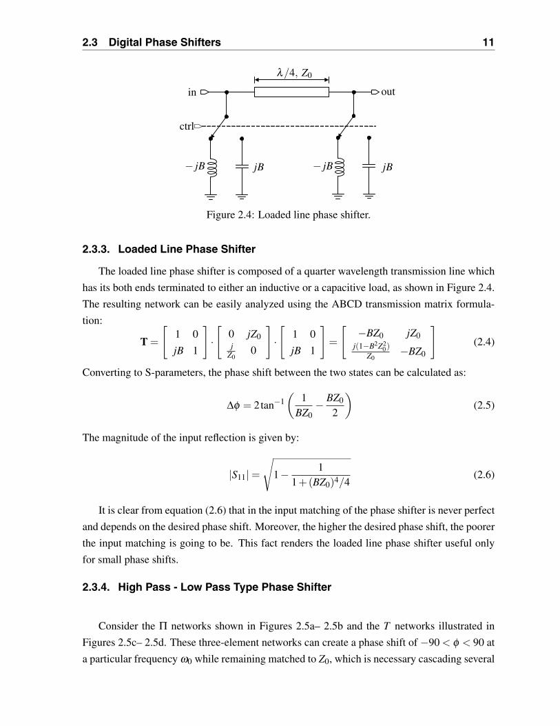
λ/4, Z0
− jB− jB jBjB
in out
ctrl
Figure 2.4: Loaded line phase shifter.
2.3.3. Loaded Line Phase Shifter
The loaded line phase shifter is composed of a quarter wavelength transmission line which
has its both ends terminated to either an inductive or a capacitive load, as shown in Figure 2.4.
The resulting network can be easily analyzed using the ABCD transmission matrix formula-
tion:
T =
[1 0
jB 1
]·[
0 jZ0j
Z00
]·[
1 0
jB 1
]=
[−BZ0 jZ0
j(1−B2Z20)
Z0−BZ0
](2.4)
Converting to S-parameters, the phase shift between the two states can be calculated as:
Δφ = 2tan−1(
1BZ0
− BZ0
2
)(2.5)
The magnitude of the input reflection is given by:
|S11|=√
1− 11+(BZ0)4/4
(2.6)
It is clear from equation (2.6) that in the input matching of the phase shifter is never perfect
and depends on the desired phase shift. Moreover, the higher the desired phase shift, the poorer
the input matching is going to be. This fact renders the loaded line phase shifter useful only
for small phase shifts.
2.3.4. High Pass - Low Pass Type Phase Shifter
Consider the Π networks shown in Figures 2.5a– 2.5b and the T networks illustrated in
Figures 2.5c– 2.5d. These three-element networks can create a phase shift of −90 < φ < 90 at
a particular frequency ω0 while remaining matched to Z0, which is necessary cascading several

12 Phase Shifter Architectures
of these networks. The design equations are provided below [18]:
For the low-pass Π network, −90 < φ < 0 (Figure 2.5a):
L =Z0 sin |φ |
ω0(2.7)
C =tan |φ/2|
ω0Z0(2.8)
For the high-pass Π network, 0 < φ < 90 (Figure 2.5b):
L =Z0
ω0 tan |φ/2| (2.9)
C =1
ω0Z0 sin |φ | (2.10)
For the low-pass T network, −90 < φ < 0 (Figure 2.5c):
L =Z0 tan |φ/2|
ω0(2.11)
C =sin |φ |ω0Z0
(2.12)
For the high-pass T network, 0 < φ < 90 (Figure 2.5d):
L =Z0
ω0 sin |φ | (2.13)
C =1
ω0Z0 tan |φ/2| (2.14)
Two types of phase shifters can be constructed using these networks [16, 18]. The first
type switches between one of the networks described above and a bypass line as illustrated in
Figures 2.6a – 2.6d. This shifter can produce a relative phase shift 0◦ < Δφ < 90◦ between
its two states. The other type of phase shifter switches between a High-pass and a Low-pass
network as illustrated in Figures 2.7a – 2.7b, resulting in a relative phase shift of 0◦ < Δφ <
180◦.
The high-pass – low-pass phase shifters can result in very compact size when realized in
integrated circuit form with spiral inductors and MiM capacitors. Furthermore, the broadband
characteristics of the of the T and Π networks allow operation over at least an octave band-
width [16]. Nevertheless, as mentioned before, the large number of switches utilized requires
an advanced CMOS process to minimize the loss at frequencies above 50GHz.

2.3 Digital Phase Shifters 13
L
CC
(a) Low-pass Π network.
LL
C
(b) High-pass Π network.
LL
C
(c) Low-pass T network.
L
CC
(d) High-pass T network.
Figure 2.5: Π and T networks.
L CC
in outctrl
(a) Switched Low-pass Π – Bypass phase shifter.
LL C
in outctrl
(b) Switched High-pass Π – Bypass phase shifter.
LL
C
in outctrl
(c) Switched Low-pass T – Bypass phase shifter.
L
CC
in outctrl
(d) Switched High-pass T – Bypass phase shifter.
Figure 2.6: Switched – bypass phase shifters.

14 Phase Shifter Architectures
L
LL
C
CC
in outctrl
(a) Switched High-pass – Low-pass Π phase shifter.
L
LL
C
CC
in outctrl
(b) Switched High-pass – Low-pass T phase shifter.
Figure 2.7: Switched high-pass – low-pass phase shifters.
22.5◦ 45◦ 90◦ 180◦
Bit0 Bit1 Bit2 Bit3
in out
Figure 2.8: Cascade of four single phase shift bits resulting in a phase shifter with 16 states.
2.3.5. Multibit Digital Phase shifters
A simple way to create a multibit digital phase shifter is to cascade a number of single-bit
phase shifters. The phase shift that each bit should introduce is decided based on the desired
phase shift range and resolution. For example if 360◦ are required in sixteen, 22.5◦ steps, the
arrangement of Figure 2.8 is possible. In this arrangement, each network switches between 0◦
and its corresponding phase shift as controlled by bits Bit0 - Bit3. The total phase shift will be
given by:
Δφ = 22.5◦ ×Bit0 +45◦ ×Bit1 +90◦ ×Bit2 +180◦ ×Bit3 (2.15)
The shortcoming of this approach it that the loss of each phase shift bit adds resulting in
high loss. For example, in [18] 10dB loss at 30GHz is reported.
A second, distributed approach is depicted in Figure 2.9 and is similar to the one presented
in [19]. A transmission line is periodically tapped so that the input signal is delayed by τD at
the input and output of every tap. Only one tap is selected for every state and the corresponding
delay for the nth bit is:
Δτ = 2nτD (2.16)
where τD is the delay introduced by each transmission line section.
There is a parasitic amplitude modulation resulting from the transmission line loss. The
loss when the nth tap is switched is 2nαl where αl is the loss of each section. Techniques to
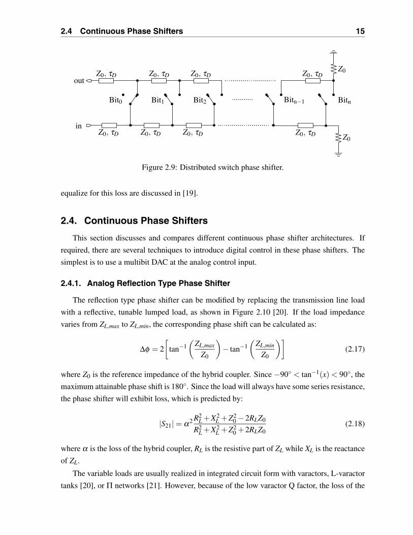
2.4 Continuous Phase Shifters 15
Z0, τD Z0, τD Z0, τD Z0, τD
Z0, τDZ0, τDZ0, τDZ0, τD
Z0
Z0
Bit0 Bit1 Bit2 Bitn−1 Bitn
in
out
Figure 2.9: Distributed switch phase shifter.
equalize for this loss are discussed in [19].
2.4. Continuous Phase Shifters
This section discusses and compares different continuous phase shifter architectures. If
required, there are several techniques to introduce digital control in these phase shifters. The
simplest is to use a multibit DAC at the analog control input.
2.4.1. Analog Reflection Type Phase Shifter
The reflection type phase shifter can be modified by replacing the transmission line load
with a reflective, tunable lumped load, as shown in Figure 2.10 [20]. If the load impedance
varies from ZL,max to ZL,min, the corresponding phase shift can be calculated as:
Δφ = 2
[tan−1
(ZL,max
Z0
)− tan−1
(ZL,min
Z0
)](2.17)
where Z0 is the reference impedance of the hybrid coupler. Since −90◦ < tan−1(x)< 90◦, the
maximum attainable phase shift is 180◦. Since the load will always have some series resistance,
the phase shifter will exhibit loss, which is predicted by:
|S21|= α2 R2L +X2
L +Z20 −2RLZ0
R2L +X2
L +Z20 +2RLZ0
(2.18)
where α is the loss of the hybrid coupler, RL is the resistive part of ZL while XL is the reactance
of ZL.
The variable loads are usually realized in integrated circuit form with varactors, L-varactor
tanks [20], or Π networks [21]. However, because of the low varactor Q factor, the loss of the

16 Phase Shifter Architectures
ZL
ZL
in
out
Figure 2.10: Reflection type phase shifter with lumped loads.
C
LL CTCT
in out
Figure 2.11: Tunable low-pass T network.
analog reflection type phase shifter is usually very high. For example, reference [21] reports
10-12 dB at 24 GHz while [20] reports 5 dB at 6.2 GHz.
2.4.2. Tunable Filter Type Phase Shifter
The Π and T networks presented in figure 2.5 can be made tunable in order to adjust
the phase shift that the network introduces. However, both the inductors and the capacitors
must change simultaneously in order to preserve the input and output matching of the filter.
”Tunable” inductors can be realized by utilizing series capacitors along with a fixed value
inductor as illustrated in Figure 2.11 [22] for a Low-pass T network. The variable capacitors
can be realized in integrated circuits using varactors.
The reactance of the series L and CT is:
Zeq = jωL− jωCT
(2.19)
As a result, at a particular frequency ω0, Zeq can be represented by an equivalent inductance:
Leq = L− 1
ω20CT
(2.20)
Solving equation (2.11) for φ yields:
|φ |= 2tan−1(
ω0Leq
Z0
)= 2tan−1
(ω0Leq
Z0− 1
ω0CT Z0
)(2.21)
2.4 Continuous Phase Shifters 17
Zi, lZi, lZi, l
CVCVCV
in out
Figure 2.12: Periodically loaded line phase shifter.
Assuming that CT can vary from CT,min to CT,max, the corresponding phase shift is:
|Δφ |= 2tan−1(
ω0Leq
Z0− 1
ω0CT,maxZ0
)−2tan−1
(ω0Leq
Z0− 1
ω0CT,minZ0
)(2.22)
In order to preserve the matching to Z0, C must also vary as:
Cmax =sin |φmax|
ω0Z0(2.23)
Cmin =sin |φmin|
ω0Z0(2.24)
where,
|φmax|= 2tan−1(
ω0Leq
Z0− 1
ω0CT,maxZ0
)(2.25)
|φmin|= 2tan−1(
ω0Leq
Z0− 1
ω0CT,minZ0
)(2.26)
The tunable filter phase shifter is very attractive for integrated circuit implementation be-
cause of its highly compact size. Nevertheless, the assumption (2.20) is valid only for a 10 -
20 % bandwidth [22]. Furthermore, the attainable phase shift is limited by the varactor capaci-
tance ratio. The loss of the phase shifter is also dominated by the varactor resistance, resulting
in high loss as the frequency increases.
2.4.3. Periodically Loaded Transmission Line Phase Shifter
The periodically loaded line phase shifter is depicted in figure 2.12 [23] and is composed
of a transmission line that is periodically tapped with varactors. By varying the capacitance of
the varactors, the characteristics of the resulting synthetic transmission line can also be varied.
The transmission line unit cell is assumed to have characteristic impedance Zi, phase ve-

18 Phase Shifter Architectures
locity vi and length l. The equivalent inductance and capacitance of each section is:
Lt =lZi
vi(2.27)
Ct =l
Zivi(2.28)
The resulting synthetic transmission line’s cut-off frequency is:
fT =1
π√
Lt(Ct +CV )(2.29)
For frequencies below the cut-off frequency, the synthetic transmission line parameters are:
ZL =
√Lt
Ct +CV(2.30)
vφ =
√l
Ll(Cl +CV )(2.31)
The loading factor of the transmission line is defined as
x =CV,max
Ct(2.32)
whereas the ratio of the minimum to maximum varactor capacitance is also defined as:
y =CV,min
CV,max(2.33)
Assuming that the characteristic impedance of the synthetic line is required to be 50Ω when
CV =CV,max, the phase shift per each section is [23]:
Δφ = 2π flvi
(√1+ x−
√1+ xy
)(2.34)
The above formula is valid under the assumption that f << fT . Since τD =− dφdω , the periodi-
cally loaded line phase shifter in fact creates time delay as long as f << fT :
Δτ =lvi
(√1+ x−
√1+ xy
)(2.35)
If the sections of length l are assumed to be lossless, the insertion loss due to the varactors
2.4 Continuous Phase Shifters 19
Zctrl
in
out
Figure 2.13: Dual gate phase shifter.
is [23]:
IL = nsectionπffs
ZL (2.36)
where nsection is the number of sections and fs is the varactor cut-off frequency:
fs =1
2πriCV,max(2.37)
where ri is the varactor series resistance.
The periodically loaded line phase shifter can achieve 360◦ of phase shift with a moderate
number of sections. Moreover, if designed properly [23], the transmission line loss could be
minimized. Nevertheless, as with many other phase shifter topologies suggested up to now, the
low quality factors of the varactors at mm-wave frequencies overwhelms the loss and renders
the phase shifter impractical for this frequency range.
2.4.4. Dual Gate FET Type Phase Shifter
The dual gate FET type phase shifter originates from dual gate MESFETs which can be
fabricated as a separate device in GaAs processes, essentially by sharing a common junction
between two FETs. Although this also possible is possible in CMOS, a more suitable version
of the phase shifter is illustrated in Figure 2.13 [24], where the dual gate device is replaced by
a cascode configuration. The impedance Z located at the gate of the common source transistor
causes a parallel resonance with the gate source capacitance and thus maximizing the available
gain and phase shift. The phase shift is controlled through the gate biasing of the common
source transistor.
The dual gate phase shifter is simple compact and can have gain. However, it can only
create small phase shifts, less than 90◦. Furthermore, the gain and phase shift are interrelated,
resulting in severe gain variation as the phase shift varies. Reference [24] reports more than 6
20 Phase Shifter Architectures
InIQ Splitter
Phase Rotator
+Out
(a) Phase interpolation phase shifter block diagram.
AI
AQ
φ
(b) I-Q phase vector synthesis.
Figure 2.14: Phase interpolation phase shifter.
dB of gain variation for 60◦ of phase variation.
2.4.5. Phase Interpolation Phase Shifter
The phase interpolation phase shifter was originally introduced in [25] and its block level
diagram is shown in Figure 2.14a. The input signal is first split into two equal amplitude in-
phase and quadrature components. In the next stage, the two components are independently
amplified by two variable gain amplifiers (VGAs) and then summed, forming the output signal.
Depending on the gain of the two VGAs, any phase between 0◦ and 360◦ can be synthesized.
The weighted summation of the I and Q components is sometimes called phase rotation and is
graphically shown in Figure 2.14b.
In order to analyze the phase interpolation phase shifter, we utilize phasor representations
for the signals and we assume that all the blocks are conjugately matched at their input and
output (i.e. there are no reflections). Furthermore, each VGA is assumed to be able to vary its
gain in the [−A,A] range. In the following analysis the signals will be represented using the
phasor notation.
The input signal is:
Vin = vin∠0◦ (2.38)
Assuming that the I-Q splitting network is passive, the I and Q outputs are:
VI =vin√
2∠0◦ (2.39)
VQ =vin√
2∠−90◦ (2.40)
If the gain of the I and Q VGAs is AI and AQ respectively, the signal at the output of the phase

2.4 Continuous Phase Shifters 21
rotator is:
Vout = AIVI +AQVQ =AIvin√
2∠(0◦ −wI180◦)+
AQvin√2
∠(−90◦ −wQ180◦) (2.41)
where
wI =
{0 if AI ≥ 0
1 if AI < 0(2.42)
wQ =
{0 if AQ ≥ 0
1 if AQ < 0(2.43)
Performing the vector addition at the right hand side of (2.41) yields the output phasor:
|Vout |= vin√2
[(|AI|cos
(0◦ −wI180◦
)+ |AQ|cos
(−90◦ −wQ180◦))2
+
+
(|AI|sin
(0◦ −wI180◦
)+ |AQ|sin
(−90◦ −wQ180◦))2
] 12
=
=vin√
2
√(|AI|cos
(0◦ −wI180◦
))2+(|AQ|sin
(−90◦ −wQ180◦))2
=vin√
2
√|AI|2 + |AQ|2
(2.44)
and
φ = ∠Vout = 180◦k+ tan−1
[|AI|sin
(0◦ −wI180◦
)+ |AQ|sin
(−90◦ −wQ180◦)
|AI|cos(0◦ −wI180◦
)+ |AQ|cos
(−90◦ −wQ180◦)]=
= 180◦k+ tan−1
[|AQ|sin
(−90◦ −wQ180◦)
|AI|cos(0◦ −wI180◦
)]
(2.45)
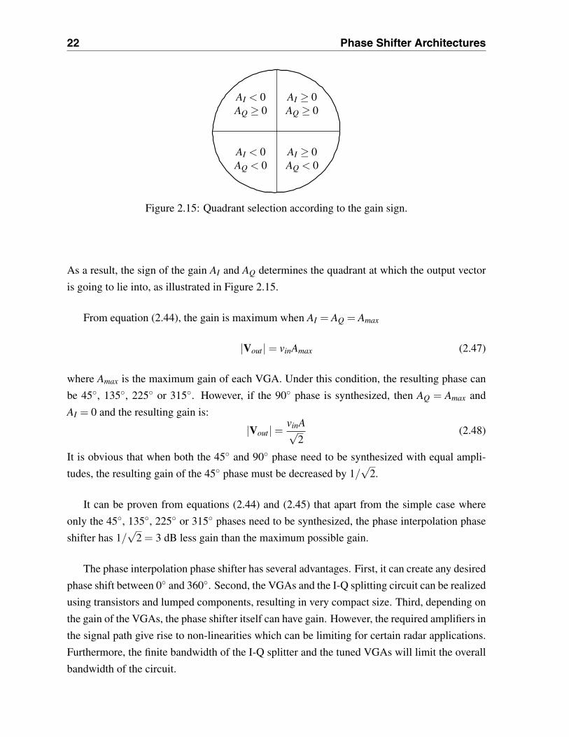
where k = 0, ±1, ±2, . . . represents the infinite solutions of the transcendental equation.
Equation (2.45) can be simplified by expanding it according to the various values of wI and
wQ:
φ =
⎧⎪⎪⎪⎪⎪⎪⎨⎪⎪⎪⎪⎪⎪⎩
tan−1( |AQ|
|AI |)
if AI ≥ 0, AQ ≥ 0
180◦ − tan−1( |AQ|
|AI |)
if AI < 0, AQ ≥ 0
180◦+ tan−1( |AQ|
|AI |)
if AI < 0, AQ < 0
− tan−1( |AQ|
|AI |)
if AI ≥ 0, AQ < 0
(2.46)
22 Phase Shifter Architectures
AI ≥ 0AQ ≥ 0
AI < 0AQ ≥ 0
AI < 0AQ < 0
AI ≥ 0AQ < 0
Figure 2.15: Quadrant selection according to the gain sign.
As a result, the sign of the gain AI and AQ determines the quadrant at which the output vector
is going to lie into, as illustrated in Figure 2.15.
From equation (2.44), the gain is maximum when AI = AQ = Amax
|Vout |= vinAmax (2.47)
where Amax is the maximum gain of each VGA. Under this condition, the resulting phase can
be 45◦, 135◦, 225◦ or 315◦. However, if the 90◦ phase is synthesized, then AQ = Amax and
AI = 0 and the resulting gain is:
|Vout |= vinA√2
(2.48)
It is obvious that when both the 45◦ and 90◦ phase need to be synthesized with equal ampli-
tudes, the resulting gain of the 45◦ phase must be decreased by 1/√
2.
It can be proven from equations (2.44) and (2.45) that apart from the simple case where
only the 45◦, 135◦, 225◦ or 315◦ phases need to be synthesized, the phase interpolation phase
shifter has 1/√
2 = 3 dB less gain than the maximum possible gain.
The phase interpolation phase shifter has several advantages. First, it can create any desired
phase shift between 0◦ and 360◦. Second, the VGAs and the I-Q splitting circuit can be realized
using transistors and lumped components, resulting in very compact size. Third, depending on
the gain of the VGAs, the phase shifter itself can have gain. However, the required amplifiers in
the signal path give rise to non-linearities which can be limiting for certain radar applications.
Furthermore, the finite bandwidth of the I-Q splitter and the tuned VGAs will limit the overall
bandwidth of the circuit.

2.5 Phase Shifter Architecture Summary 23
2.5. Phase Shifter Architecture Summary
The table below summarizes the basic properties of the phase shifters presented thus far.
The phase shift range of every phase shifter is also provided in the table. Nevertheless, as with
digital shifters, the phase shift range of analog phase shifters can be extended by cascading
several of them. The penalty of this extension is again the increased loss of the resulting
system.
Type Analog /
Digital
Constant Phase /
True Time Delay
Phase Shift Range
Switched Line Digital True Time Delay (0,∞)
Reflection Digital True Time Delay (0,∞)
Loaded Line Digital Constant Phase (0,180)
High Pass - Low Pass Digital Constant Phase (0,180)
Distributed Switch Digital True Time Delay (0,∞)
Analog Reflection Analog Constant Phase (0,180)
Tunable Filter Analog Constant Phase (0,90)
Periodically Loaded T-line Analog True Time Delay (0,∞)
Dual Gate Analog Constant Phase (0,90)
Phase Interpolation Analog Constant Phase (0,360)
2.6. Other Applications of Phase Shifters
Perhaps the most important and widely used application of phase shifters is that of phased
arrays, as discussed in section 1.1. In this section, two other well established applications are
analyzed.
2.6.1. I-Q Calibration
A generic Hartley quadrature wireless receiver front-end is depicted in Figure 2.16a. This
receiver architecture or its heterodyne equivalent is present in almost every modern wireless
system. It is a well documented [26, 27] fact that phase imbalance in the I-Q splitter degrades
the performance of the receiver. In the case of a heterodyne receiver, it degrades the image
rejection ratio (IRR) whereas in a direct conversion receiver, the imbalance causes cross-talk
between the data modulated in the I and Q paths.
A possible solution to the I-Q imbalance problem is illustrated in figure 2.16b. In this
case, two high-resolution phase shifters with small phase shift range are placed in the I and Q
paths, after the I-Q splitting. When an appropriate, known test vector is applied at the input

24 Phase Shifter Architectures
RFIN
LNA
90◦
IFI IFQ
(a) I-Q receiver.
RFIN
LNA
90◦
IFI IFQ
φ φ
(b) I-Q receiver with calibration.
Figure 2.16: I-Q receiver architectures.
of the receiver, any possible I-Q imbalance could be detected by the baseband Digital Signal
Processor which in turn, can set the appropriate phase shift in the phase shifters to correct the
I-Q imbalance.
Although I-Q imbalance could be fully corrected by the baseband DSP [28], the scheme of
figure 2.16b is more appropriate for multi-gigabit mm-wave radios since it reduces the already
severe computational burden of the DSP.
2.6.2. Frequency Translators - Modulators
Consider the system of Figure 2.17 where an analog 0◦ − 360◦ phase shifter has it phase
control input modulated with a continuous ramp with slope of r degrees/sec. A constant fre-
quency sinusoid of frequency fref is applied at the high frequency input of the phase shifter.
The output of the phase shifter is:
RFout = cos(freft +Δφ) = cos(freft + rt) = cos(fref + r)t (2.49)
Therefore, the frequency of the input signal can be shifted in frequency by r or −r depending
on the slope of the ramp. This circuit is known as frequency translator and dates back to the
days of microwave ferrite phase shifters which could be used to adjust the frequency of a known
reference.
2.7 Conclusion 25
fref
InputRamp
φ out
Figure 2.17: Frequency translator.
Equation (2.49) can be seen from another point of view. The input carrier is modulated by
another sinusoid in one of its two sidebands. As a result, a phase shifter can be utilized as a
frequency or phase modulator.
2.7. Conclusion
This chapter presented the various phase shifter architectures encountered in the literature
and can be realized in standard integrated circuit form. Mathematical analysis was provided
for the various topologies and their main advantages and disadvantages were discussed.

26 Phase Shifter Architectures

3Analysis and Design Of
Phase Interpolation Phase
Shifters
3.1. Choice of Phase Shifter Topology
The main goal of this work is the development of a transmitter (TX) and a receiver (RX)
with phase shifting. The transmitter and receiver need to be capable of being integrated in a
phased array system, which could be assembled by using only multiple copies of them and
an in-phase power combiner or divider. The target frequencies for the arrays are 77GHz and
94GHz.
As discussed in section 1.1, a phased array can either use true time delay phase shifters
of constant-phase phase shifters. All time delay elements need transmission lines in order to
realize time delays. Assuming that the effective dielectric constant of a transmission line in
silicon is εe f f = 3.8, the resulting length of a λ/4 transmission line which would be needed
to create a 90◦ phase shift is 500μm at 77GHz and 410μm at 94GHz. Even if the loss of
these lines is small in the case of a thick metallization process, their size is prohibitively large
since several of these lines would be required in a phase shifter. As a result, the use of a
constant-phase phase shifter was decided.
Most of the passive constant-phase phase shifters require varactors to realize tunable ele-
ments. However, the varactor Q factor is ranging from 6-8 at 94GHz in 65-nm CMOS [29] and
5-10 for 130-nm SiGe BiCMOS at 77GHz [30]. These low Q factors would result in very high
loss which would be very difficult and power intensive to be compensated using amplifiers. For
example, reference [31] presents a loaded line phase shifter with 9.4dB loss at 60GHz, while
reference [21] reports 10− 12dB at 24GHz for a reflection type phase shifter. A different
choice would be the High-Pass Low-Pass phase shifter as in section 2.3.4. However, in order
to attain, for example, a 0◦ − 360◦ phase shift range in 22.5◦ steps, four such phase shifters
need to be cascaded, resulting in high loss. Examples of High-Pass Low-Pass phase shifter can
be found in [18] and [32] where the losses are 10dB at 30GHz (4 bits) and 20dB at 12GHz
(5 bits) respectively. It should be also noted that these losses are going be further exacerbated
27

28 Analysis and Design Of Phase Interpolation Phase Shifters
0◦
0◦
90◦
90◦In Out
Figure 3.1: Interpolation phase shifter utilizing differential signals.
at the target frequencies of 77GHz and 94GHz and would most likely result in a non-practical
phase shifter.
Driven by these facts, the phase interpolation phase shifter was selected. The topology was
preferred because of its potential to have low loss, its ability to easily obtain 0◦ − 360◦ phase
shift range and its very compact size. It’s major disadvantage is its potentially poor linearity
which can be a major issue in certain radar applications. However, this issue could be partially
corrected in the circuit design of the variable gain amplifiers.
3.2. System Analysis of the Phase Interpolation Phase Shifter
The basic theory behind the interpolation phase shifter was presented in section 2.4.5. In
order to be able to synthesize phases in all four quadrants, the variable gain amplifiers need to
have both positive and negative gain. To accomplish this, the VGAs have to be differential so
that their two outputs could be flipped and cause a sign inversion. A more detailed version of
the phase shifter, utilizing differential signals, is illustrated in Figure 3.1 where the differential
splitting and combining is done using transformers. The input signal is first split into two parts
of equal amplitude. The normalized phase of the two signals can be considered to be 0◦ and
180◦ respectively. Similarly, the normalized phases at the output of the first I-Q splitter are 0◦
and 90◦ whereas, at the output of the second splitter, the phases are 180◦ and 270◦. Rearranging
the signals, the phases at the input of the first VGA are 0◦ and 180◦ while the phases at the
input of the second VGA are 90◦ and 270◦. The outputs of the VGAs are summed in current,
as will be shown in the phase rotator section, and the output is converted to single ended using
a second transformer.
The mathematical analysis is essentially the same as presented in section 2.4.5. The ra-
tio of the gains of the two VGAs can be calculated, based on the desired phase shift, using
equation (2.45):
RI/Q =AQ
AI= tanφ (3.1)

3.3 Error Model for the Interpolation Phase Shifter 29
If a phase shift in the range of 0◦ − 360◦ is required in N steps, there are two possible
arrangements. First, the N phases could be arranged as 0, 360◦/N, 2×360◦/N, . . . , (N−1)×360◦/N. A second arrangement is possible if a constant phase offset of 360◦/2N is added to
every phase shift state, resulting in: 360◦/2N, 3× 360◦/2N, 5× 360◦/2N, . . . , (2N − 1)×360◦/2N. Table 3.1 shows the ratio RI/Q of the VGA gains when N = 16 for the two phase
arrangements. The arrangement without phase offset results in a VGA that needs infinite gain
adjustment range whereas the arrangement with 11.25◦ offset requires a VGA with only 14dB
of gain adjustment range.
When RI/Q is known based on the phase requirements, the individual gains of the VGAs
can be calculated based on the requirement that all phase states have equal amplitudes. If the
maximum VGA gain is normalized to 1 (0dB), solving equation (2.44) yields:
AI =1√
1+R2I/Q
(3.2)
AQ =RI/Q√
1+R2I/Q
(3.3)
The normalized gain of each phase is −3dB, i.e., 3dB lower than the gain of the individual
VGA. Table 3.2 illustrates AI and AQ, along with their signs, for case of N = 16. The phase
arrangement with 11.25◦ offset will be utilized in the design of the interpolation phase shifter
in this work because of its reduced dynamic range requirement.
3.3. Error Model for the Interpolation Phase Shifter
The analysis up to now assumed that all the components used in the system are ideal.
Nevertheless, there are various sources of imperfections that can result in both amplitude and
phase error in the interpolation phase shifter. The most important of these include:
• Transformer balun amplitude and phase imbalance. Due to modeling imperfections and
process variations, the transformers used in at the input and output in figure 3.1 will not
split the signal exactly in two equal parts and these parts will not be precisely 180◦ out
of phase.
• Quadrature splitter amplitude and phase imbalance. As with the transformers, the outputs
of the quadrature splitters will not be exactly equal, or 90◦ out of phase.
• Variable gain amplifier phase stability. Up to now we have assumed that the phase shift
introduce by the VGAs is constant as their gain varies. In all practical VGAs though, the
phase can vary significantly as the amplitude changes.

30 Analysis and Design Of Phase Interpolation Phase Shifters
Phase Shift AQ/AI AQ/AI (11.25◦offset)
0◦ 0 0.2
22.5◦ 0.414 0.66845◦ 1 1.497
67.5◦ 2.414 5.02790◦ ∞ -5.027
112.5◦ -2.414 -1.497135◦ -1 -0.668
157.5◦ -0.414 -0.2180◦ 0 0.2
202.5◦ 0.414 0.668225◦ 1 1.497
247.5◦ 2.414 5.027270◦ ∞ -5.027
292.5◦ -2.414 -1.497315◦ -1 -0.668
337.5◦ -0.414 -0.2Gain Range ∞ 14dB
Table 3.1: RI/Q for different phase shifts and phase arrangements.
Phase Shift Sign AI (dB) Sign AQ (dB) Sign AI (dB)11.25◦offset
Sign AQ (dB)11.25◦offset
0◦ + 0 ø −∞ + 0 + -1422.5◦ + -0.69 + -8.34 + -1.43 + -4.9445◦ + -3 + -3 + -4.94 + -1.43
67.5◦ + -8.34 + -0.69 + -14 + 090◦ ø −∞ + 0 - -14 + 0
112.5◦ - -8.34 + -0.69 - -4.94 + -1.43135◦ - -3 + -3 - -1.43 + -4.94
157.5◦ - -0.69 + 8.34 - 0 + -14180◦ - 0 ø −∞ - 0 - -14
202.5◦ - -0.69 - -8.34 - -1.43 - -4.94225◦ - -3 - -3 - -4.94 - -1.43
247.5◦ - -8.34 - -0.69 - -14 - 0270◦ ø −∞ - 0 + -14 - 0
292.5◦ + -8.34 - -0.69 + -4.94 - -1.43315◦ + -3 - -3 + -1.43 - -4.94
337.5◦ + -0.69 - -8.34 + 0 - -14
Table 3.2: AI and AQ for different phase shifts and arrangements.

3.3 Error Model for the Interpolation Phase Shifter 31
The amplitude and phase imbalance of the transformer balun and IQ splitter can be modeled
based on the passivity relation of their scattering parameter matrix [33]. Since the transformer
is passive its two outputs, including possible errors will be:
V◦0 = αde j·0◦ (3.4)
V180◦ =√
1−α2d e j·(180◦+φe,180◦) (3.5)
where 0 ≤ αd ≤ 1 and −90◦ ≤ φe,180◦ ≤ 90◦. αd = 1/√
2 and φe,180◦ = 0◦ when no errors are
present. The transformer amplitude imbalance is defined as
Ae,180◦ = 20log
(αd√
1−α2d
)(3.6)
Similarly, the passivity relations of the IQ splitter yield:
V◦0 = αIQe j·0◦ (3.7)
V90◦ =√
1−α2IQe j·(90◦+φe,90◦) (3.8)
where 0 ≤ αIQ ≤ 1 and and −45◦ ≤ φe,90◦ ≤ 45◦. αIQ = 1/√
2, φe,90◦ = 0◦ when errors are not
considered. The amplitude imbalance is also defined by:
Ae,90◦ = 20log
(αIQ√
1−α2IQ
)(3.9)
In the VGA case, the assumption of linear phase variation is made. At a certain frequency,
the transmission phase of the VGA is assumed to vary linearly as the gain varies:
φ(S21) = φr(◦/dB) · |S21|(dB) (3.10)
Simulation and measurement results that will presented later in the thesis will confirm the
validity of this linear model. The phase shift is assumed to be independent of the gain sign.
In order to analyze the impact of each non-ideality in the phase shifter, each source of error
is considered separately. The result is analyzed using two methods: first, the polar diagram
of the transfer (S21) parameter of the phase shifter for all different phase states is generated.
Second, the maximum possible phase error between two consecutive states and the peak-to-
peak gain deviation between all states are computed.

32 Analysis and Design Of Phase Interpolation Phase Shifters
-0.5 0.0 0.5
-0.5
0.0
0.5
Real
Imag
inar
y
Ae,90◦ = 1.5dB
(a) Distortion when Ae,90◦ = 1.5dB.
-0.5 0.0 0.5
-0.5
0.0
0.5
Real
Imag
inar
y
φe,90◦ = 10◦
(b) Distortion when φe,90◦ = 10◦
-0.5 0.0 0.5
-0.5
0.0
0.5
Real
Imag
inar
y
Ae,180◦ = 1.5dB
(c) Distortion when Ae,180◦ = 1.5dB.
-0.5 0.0 0.5
-0.5
0.0
0.5
Real
Real
Imag
inar
y
φe,180◦ = 10◦
(d) Distortion when φe,180◦ = 10◦.
-0.5 0.0 0.5
-0.5
0.0
0.5
Real
Imag
inar
y
φr = 3◦/dB
(e) Distortion when φr = 3◦/dB.
Figure 3.2: Phase shifter signal constellation under various errors.

3.3 Error Model for the Interpolation Phase Shifter 33
Error Condition MaximumAmplitude Error
Maximum PhaseError
Ae,90◦ = 1.5dB 1.4 dB 9.5◦φe,90◦ = 10◦ 1.4 dB 6.5◦
Ae,180◦ = 1.5dB 0.1 dB 0.4◦φe,180◦ = 10◦ 0.1 dB 0.4◦
φr = 3◦ 2.3 dB 5.4◦Monte Carlo
σ(Ae,90◦) = σ(Ae,180◦) = 0.2dBσ(φe,90◦) = σ(φe,180◦) = 2◦
σ(φr) = 0.5◦
5.6 dB 18◦
Table 3.3: Phase and amplitude errors of the phase shifter.
Figures 3.2a and 3.2b show the distortion of the polar diagram when the amplitude imbal-
ance and phase error of the quadrature splitter are Ae,90◦ = 1.5dB and φe,90◦ = 10◦ respectively.
In both cases, the diagram is distorted and gets an elliptic shape. Moreover, amplitude imbal-
ance in the I-Q splitter results in both amplitude and phase error in the phase shifter. The same
case holds for the phase imbalance in the splitter.
Figures 3.2c and 3.2d illustrate the distortion when the amplitude imbalance and phase
error of the transformer balun are Ae,180◦ = 1.5dB and φe,180◦ = 10◦. The amplitude imbalance
case causes a negligible distortion in the third quadrant of the diagram (where both AI and AQ
are negative). The phase error case adds a constant phase offset without adding a phase error
to the final points.
Figure 3.2e depicts the distortion in the polar diagram when the phase shift introduced by
the VGA is φr = 3◦/dB. The diagram is severely distorted, with both phase and amplitude
error. The resulting shape is rectangular with ”curled” sides.
Table 3.3 summarizes the peak-to-peak amplitude and phase error of each of the cases
discussed above. It can be seen that the most severe error source is the phase variation with
gain in the VGAs. A significant error source can also be the phase and amplitude imbalance in
the I-Q splitter.
In order to study the overall effect when all error sources are present, a Monte Carlo
simulation is utilized. The error sources are assumed to follow uncorrelated normal distri-
butions. The average values of the distributions are set as: μ(Ae,90◦) = μ(Ae,180◦) = 0dB,
μ(φe,90◦) = μ(φe,180◦) = 0◦ μ(φr) = 1◦. The deviations are set as: σ(Ae,90◦) = σ(Ae,180◦) =
0.2dB σ(φe,90◦) = σ(φe,180◦) = 2◦ σ(φr) = 0.5◦. The resulting I-Q diagram is shown in Fig-
ure 3.3 and the maximum phase shifter errors are summarized in table 3.3. It is clear that when
all the sources of error are present, large errors are possible in the phase shifter. This fact is
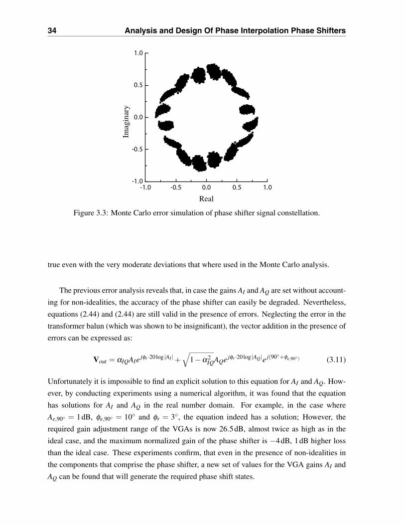
34 Analysis and Design Of Phase Interpolation Phase Shifters
-1.0 -0.5 0.0 0.5 1.0-1.0
-0.5
0.0
0.5
1.0
Real
Imag
inar
y
Figure 3.3: Monte Carlo error simulation of phase shifter signal constellation.
true even with the very moderate deviations that where used in the Monte Carlo analysis.
The previous error analysis reveals that, in case the gains AI and AQ are set without account-
ing for non-idealities, the accuracy of the phase shifter can easily be degraded. Nevertheless,
equations (2.44) and (2.44) are still valid in the presence of errors. Neglecting the error in the
transformer balun (which was shown to be insignificant), the vector addition in the presence of
errors can be expressed as:
Vout = αIQAIejφr·20log |AI |+
√1−α2
IQAQe jφr·20log |AQ|e j(90◦+φe,90◦) (3.11)
Unfortunately it is impossible to find an explicit solution to this equation for AI and AQ. How-
ever, by conducting experiments using a numerical algorithm, it was found that the equation
has solutions for AI and AQ in the real number domain. For example, in the case where
Ae,90◦ = 1dB, φe,90◦ = 10◦ and φr = 3◦, the equation indeed has a solution; However, the
required gain adjustment range of the VGAs is now 26.5dB, almost twice as high as in the
ideal case, and the maximum normalized gain of the phase shifter is −4dB, 1dB higher loss
than the ideal case. These experiments confirm, that even in the presence of non-idealities in
the components that comprise the phase shifter, a new set of values for the VGA gains AI and
AQ can be found that will generate the required phase shift states.

3.4 I-Q Splitting 35
Inp
Inn
Ip
Qn
Qp
InC
C
L
L
2R
2R
Figure 3.4: All-Pass polyphase filter.
3.4. I-Q Splitting
An essential component of the interpolation phase shifter is the splitting of the signal into
in-phase and quadrature complements. There are several methods proposed in the bibliogra-
phy to achieve this I-Q splitting which include: High-Pass – Low-Pass filters [34], Polyphase
Filters [35, 36] and Quadrature Hybrids [33].
In this work, the different approaches a I-Q splitting were studied and compared based
on their feasibility for mm-wave frequency operation. The main problem for high frequency
operation of most I-Q splitters remains their potentially high loss or the resulting very small
component values, which could lead to process variation problems. Two different ways of
splitting were finally implemented: an All-Pass Polyphase filter [36] and a lumped quadrature
hybrid [37].
3.4.1. All-Pass Polyphase filter
The All-Pass polyphase filter was recently proposed in [36] and is shown in figure 3.4. It
consists of four RLC All-Pass filters, arranged to introduce ±45◦ phase shifts. This principle
of operation is similar to the RC polyphase filter where the ±45◦ phase shifts are created by
RC-CR filters.
The values of the resistors in figure 3.4 determine the bandwidth of operation of the filter,
its input and output characteristic impedances as well as the tolerance of the filter to variations
of its load. Although larger resistance results in increased bandwidth, the loss of the filter also
increases leading to bandwidth – loss trade-off. Once the value of the filter quality factor (and
bandwidth) Q is selected, the values of R, L and C are selected based on the desired frequency
of operation:
ω0 =1√LC
(3.12)
Q =
√L/C
R

36 Analysis and Design Of Phase Interpolation Phase Shifters
80 85 90 95 100-7
-6
-5
-4
-3
-2
-1
0
89
90
91
Frequency (GHz)
S 21,
S 31
(dB
)Phase
Difference
(Degrees)
S21 −S31S21S31Phase(S21/S31)
Figure 3.5: All-Pass polyphase filter simulation results.
where ω0 is the frequency of operation.
In order to obtain large bandwidth and make the filter insensitive to poorly predictable
load variations that are common in mm-wave frequencies, a quality factor value Q = 0.25 was
selected and ω0 = 90GHz. Under these conditions, equations 3.12 yield C = 105fF, L = 33pH
and R = 75Ω. This design procedure also sets the input and output impedances of the filter to
75Ω.
The simulated response of the filter is shown in figure 3.5, where it can be seen that the filter
exhibits slightly more than ±1◦ of phase imbalance and less than 1dB of amplitude imbalance
in the 80GHz− 100GHz range. However, the price paid for this broadband behavior is the
fact that the filter has 3dB additional loss from the input to each of the I and Q outputs. This
additional loss is still much lower than the corresponding loss that would be generated by a
classical polyphase filter of similar performance.
3.4.2. Lumped Quadrature Hybrid
Quadrature hybrids have been commonly used for I-Q splitting in microwave circuits. A
quadrature hybrid can be realized utilizing different methods including: branch line couplers,
ring hybrids and coupled-line couplers. Of these methods, the coupled line couplers have been
extensively utilized because of their high bandwidth of operation. Unfortunately, the length
of the coupled lines must be λ/4 which renders their size relatively large even for mm-wave
frequencies. There have been several attempts to reduce the size of coupled line couplers, the
most important being the one described in [37, 38]. In this approach, the coupled lines are
approximated at a particular frequency ω0 with lumped elements as depicted in figure 3.6a.

3.4 I-Q Splitting 37
In I
Q
CMCM
CGCG
CGCG
R
k
L
L
(a) Fully descretized version.
In I
Q
CM1 CM2
R
k
L
L
(b) Reduced element version
Figure 3.6: Two versions of the lumped quadrature hybrid.
Each individual line is approximated with a Π network, whereas the magnetic coupling is
realized by introducing coupling between the two inductors and the capacitive coupling is
realized using lumped capacitors. The design equations are straightforward:
L = LnormZ0
ω0(3.13)
CG =CGnorm
Z0ω0(3.14)
CM =CMnorm
Z0ω0(3.15)
k = 0.707 (3.16)
where Lnorm = 1.414, CGnorm = 0.414, CMnorm = 1.
In mm-wave frequencies, application of equations (3.13 - 3.16) results in components with
impractically small values. For example, when f0 = 77GHz and Z0 = 50Ω, then L = 140pH,
CM = 41fF, CG = 17fF. Clearly the capacitors CG are very small to be reliably realized with
high Q MiM capacitors. In order to alleviate this problem, our design methodology proceeds as
follows. First, a transformer with component values as close as possible with the ones predicted
by equations (3.13) and (3.16) is designed and the 2−Π model [12] for this transformer is
extracted. The small capacitors are omitted and the resulting structure is optimized in order
to obtain a response as close as possible with the ideal one. Following this methodology, a
design centered at 85GHz is shown in figure 3.6b (L = 96pH, CM1 = 27 fF, CM1 = 40 fF
and R = 40 Ω) and its simulated response in figure 3.7. It can be seen that the lumped hybrid
coupler also exhibits slightly more than ±1◦ of phase imbalance and less than 1dB of amplitude
imbalance in the 70GHz−90GHz range. Moreover, the loss from the input to each of the two
outputs remains lower than 1dB.

38 Analysis and Design Of Phase Interpolation Phase Shifters
70 75 80 85 90-4
-3
-2
-1
0
89
90
91
Frequency (GHz)
S 21,
S 31
(dB
)Phase
Difference
(Degrees)
S21 −S31S21S31Phase(S21/S31)
Figure 3.7: Lumped quadrature hybrid simulation results.
3.5. Variable Gain Amplifiers
The variable gain amplifier is an essential component in the interpolation phase shifter.
First, it must have an adequate gain adjustment range in order for the phase shifter to generate
0◦ − 360◦ phase shift. Most importantly, as numerical experiments in section 3.2 showed, a
large gain adjustment range is required in order for the non-idealities of the phase shifter to
be corrected. Second, the transmission phase variation with gain control must be as low as
possible since it can severely alter the resulting constellation diagram of the phase shifter. Last
but not least, the overall linearity of the phase shifter will be determined by the variable gain
amplifiers because they are the only active components utilized.
There have been numerous variable gain amplifiers proposed in the literature, since a VGA
is needed in every high dynamic range receiver. There are topologies that exhibit both ana-
log [39] and digital [40] gain control. In this work, two different mm-wave VGAs have been
implemented: a 65-nm CMOS current steering VGA for the 94-GHz phase shifter and a SiGe
BiCMOS Gilbert-cell VGA for the 77-GHz phase shifter. The two VGAs utilize similar circuit
topologies. Their main difference is the way the gain control is applied.
3.5.1. 65-nm CMOS, 94 GHz Variable Gain Amplifier
The CMOS current steering VGA is shown in figure 3.8. The VGA is very similar to a
Gilbert multiplier where the cascode transistors M4-M7 are used only to control the sign of the
output signal with respect to the input. When the sign bit switches from 0 to 1.2V, the positive
and negative outputs are flipped and as a result, the phase of the output changes by 180◦. The

3.5 Variable Gain Amplifiers 39
In
M1 GainCtrl
LC
M2 M3
M4 M5 M6 M7
LMLM
signsignsignsign
Out
CdecParameter Value
WM1 2 μmWM2, WM3 16 μm
WM4 −WM7 24 μmLC 140pHLM 140pH
Cdec 500fF
Figure 3.8: 65-nm CMOS, 94 GHz CMOS variable gain amplifier.
differential input signal is applied to the gates of transistors M2 and M3 and is amplified by the
cascode formed by M2-M4 (M5 when sign = 0) and M3-M6 (M7). At DC, M1 forms a current
mirror with M2 and M3 and thus, it is able to control the bias currents of M2 and M3. As the
voltage GainCtrl is decreased from its nominal value, the current flowing through the cascodes
M2-M4 and M3-M6 is decreased. The decreasing current results in reduced effective fT in the
cascodes and consequently reduced gain.
The inductor LC helps improve the common mode rejection properties of the amplifier
whereas, inductors LM create a series resonance with the drain capacitances of M2-M3 and the
source capacitances of M4-M7, improving the overall gain of the VGA [11]. In order to ensure
high frequency stability of the amplifier, decoupling capacitors Cdec = 500fF are placed in the
gates of the common-gate transistors M4-M7.
The transistors M2 and M3 are biased at 0.3mA/μm when their gain is maximum. This
corresponds to the peak fT current density for this process and biasing at this level provides the
maximum possible gain. The resulting power consumption is 11.5mW (9.5mA from 1.2V).
A critical aspect with this VGA topology stems from the bias current variation itself. As the
bias point varies, the parasitic capacitances of the transistors will also change. As a result, the
transmission phase of the VGA will depend on the gain state. Another side effect associated
with the bias current variation is the fact that the input impedance of the VGA also changes,

40 Analysis and Design Of Phase Interpolation Phase Shifters
resulting in non-constant loading of its preceding and succeeding stages.
There are two limiting factors in the linearity of the VGA, as expressed by its input com-
pression point. First, if the input signal amplitude is very large, the gate source voltage of
transistors M2 and M3 swings below their threshold voltage and causes them to turn off. This
mode of operation is identical to class AB amplifiers and results in gain reduction at large sig-
nal amplitudes. The second limiting mechanism is the fact that the output signal swing cannot
be larger than VDD − 2VSAT, where VSAT is the drain-source saturation voltage of the MOS-
FETs. If the input signal is large enough to cause the output swing to exceed this value, the
output voltage will clip and also result in gain reduction.
When the gain of the VGA is reduced by decreasing the bias current flowing through tran-
sistors M2 and M3, the DC gate-source voltage VGS of the transistors is also reduced, resulting
in degradation of the input linearity of the amplifier. However, since the output voltage is:
vOUT = VDD −gmvin|Zout | (3.17)
and gm decreases with bias current (when the current density JDS is less than 0.15mA/μm),
the output non-linear behavior of the amplifier improves as the gain is reduced.
Based on the above analysis, the input compression point of the VGA is initially expected
to improve as the gain reduces. However, there will be a gain setting where the input non-
linearity of the M2 and M3 will dominate the linearity of the VGA. Beyond this point, there
will not be any further improvement of the compression level.
3.5.2. 130-nm SiGe BiCMOS, 77 GHz Variable Gain Amplifier
The Gilbert-cell type SiGe BiCMOS variable gain amplifier is illustrated in figure 3.9. A
BiCMOS topology with MOS transconductors was selected in order to facilitate low supply
voltage operation and high linearity. Moreover, because the pole at the drain of the MOSFET
and the emitter of the HBT is pushed beyond the HBT fT/2, the MOS-HBT cascode has higher
stability phase margin than an HBT-HBT cascode while providing over 10dB of power gain
from a lower supply [41].
The differential input signal is applied at the gates of the MOS transconductors. The gain
control is achieved by steering the current between transistors Q1-Q2 and Q3-Q4 through a
differential DC control signal applied at their bases. When maximum positive gain is required,
all the bias current is steered through transistors Q1 and Q3, while Q2 and Q4 remain off. In
order to reduce the gain, a portion of the current is steered through Q2 and Q4, resulting in
addition of the opposite phases of the input signal at the output. The sign of the gain of the
VGA can be flipped by steering the current through Q2 and Q4 instead of Q1 and Q3.

3.5 Variable Gain Amplifiers 41
In
Lin
Lin
M1 M2
LELE
LC
GainCtrl Q1 Q2 Q3 Q4
Cdec
Out
Parameter Value
WM1, WM2 16×1.125 μmlQ1−Q4 2.8 μm
LC 100pHLE 35pH
Cdec 500fF
Figure 3.9: 130-nm SiGe BiCMOS, 77 GHz variable gain amplifier.
This gain adjustment procedure has the advantage that the bias current at the transconduc-
tors M1 and M2 remains constant as the gain is varied. As a result, the input impedance of the
VGA will remain constant to a first order approximation. For the same reason, the transmission
phase versus gain is also expected to remain roughly constant. Furthermore, the gate-source
voltage of the MOS transconductors is held constant and as a result, based on similar arguments
as with the CMOS VGA, the linearity is expected to improve as the gain is reduced, until it is
completely dominated by the input non-linearity of the MOS transconductors. However, the
gain where the input non-linearity will dominate the linearity of the VGA is going to be much
lower than the corresponding one in the CMOS VGA because of the constant VGS in M1 and
M2.
Inductors Lin and LE facilitate conjugate matching with the previous stage. In addition, the
inductors LE provide series feedback in the MOS transconductors, improving their linearity,
with a penalty in the gain of the VGA. As with the 65-nm VGA, capacitors Cdec assure the
high frequency stability of the amplifier and make it immune to possible base interconnect
inductances. Similarly, inductor LC improves the common mode rejection properties of the
amplifier.
The sizing ratio between the MOS and HBT transistors is such that all transistors are biased
at the peak fT current density when the quad transistors are fully switched. The bias current
per side is 5.2mA and the power supply voltage, which is applied through the center tap of a
transformer as will be shown in the next section, is 2.5V, resulting in a total power consumption
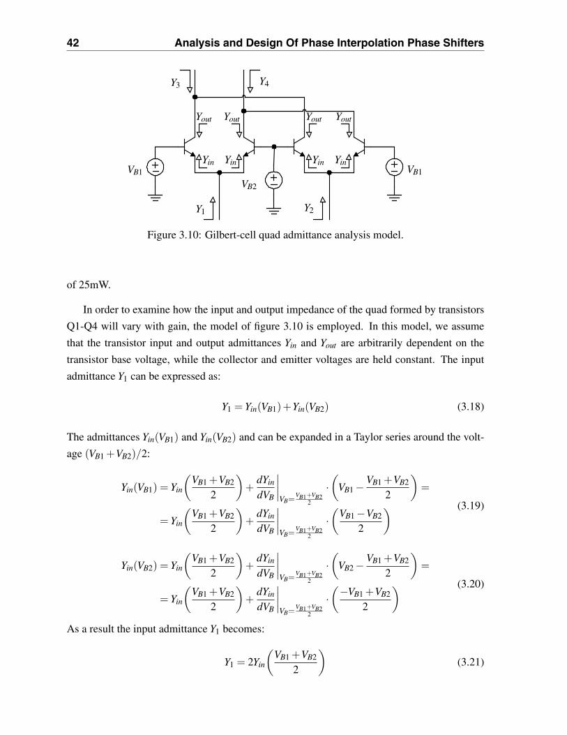
42 Analysis and Design Of Phase Interpolation Phase Shifters
Y1 Y2
YinYinYinYin
YoutYoutYoutYout
Y3 Y4
VB1VB1
VB2
Figure 3.10: Gilbert-cell quad admittance analysis model.
of 25mW.
In order to examine how the input and output impedance of the quad formed by transistors
Q1-Q4 will vary with gain, the model of figure 3.10 is employed. In this model, we assume
that the transistor input and output admittances Yin and Yout are arbitrarily dependent on the
transistor base voltage, while the collector and emitter voltages are held constant. The input
admittance Y1 can be expressed as:
Y1 = Yin(VB1)+Yin(VB2) (3.18)
The admittances Yin(VB1) and Yin(VB2) and can be expanded in a Taylor series around the volt-
age (VB1 +VB2)/2:
Yin(VB1) = Yin
(VB1 +VB2
2
)+
dYin
dVB
∣∣∣∣VB=
VB1+VB22
·(
VB1 − VB1 +VB2
2
)=
= Yin
(VB1 +VB2
2
)+
dYin
dVB
∣∣∣∣VB=
VB1+VB22
·(
VB1 −VB2
2
) (3.19)
Yin(VB2) = Yin
(VB1 +VB2
2
)+
dYin
dVB
∣∣∣∣VB=
VB1+VB22
·(
VB2 − VB1 +VB2
2
)=
= Yin
(VB1 +VB2
2
)+
dYin
dVB
∣∣∣∣VB=
VB1+VB22
·(−VB1 +VB2
2
) (3.20)
As a result the input admittance Y1 becomes:
Y1 = 2Yin
(VB1 +VB2
2
)(3.21)
3.6 Phase Rotators 43
Following the same reasoning, the remaining input and output admittances are:
Y2 = 2Yin
(VB1 +VB2
2
)(3.22)
Y3 = 2Yout
(VB1 +VB2
2
)(3.23)
Y4 = 2Yout
(VB1 +VB2
2
)(3.24)
It is clear from the above equations that the voltages VB1 and VB2 may vary independently,
but as long as their sum VB1 +VB2 is constant, the input and output admittances of the quad
will remain constant to a first order approximation. As a matter of fact, expansion with more
Taylor series terms in equations (3.19) and (3.20) reveals that all the odd terms cancel while
the even terms remain and add up. Assuming that all the series terms above the third order are
negligible, any impedance variation will come from:
d2Yin
dV 2B
∣∣∣∣VB=
VB1+VB22
·(
VB1 −VB2
2
)2
(3.25)
The above analysis reveals how the DC control voltage of the quads should be applied, i.e.
VB1 +VB2 should be held constant in order to minimize variations in Y1-Y4 with gain.
3.6. Phase Rotators
3.6.1. 65-nm CMOS, 94 GHz Phase Rotator
The 65-nm CMOS phase rotator is illustrated in figure 3.11. It is composed of two VGAs,
as presented in section 3.5.1. The outputs of the two VGAs are summed in current at the output
transformer. The transformer, apart from providing the tuned load to the circuit, it AC-couples
the output and provides differential to single ended conversion.
The sign of the gain of each VGA is selected by the two bits signI and signQ at the the top
CMOS switches of the two VGAs. This sign selection essentially also selects the quadrant of
the applied phase shift. Inside the selected quadrant, the phase is controlled in analog fashion
by changing gain through the bias currents of the common source MOSFETs in the I and Q
VGAs. A multi-bit DAC could replace the analog control in an all-digital control version.
In order to assess the performance of each VGA in the rotator, the Q input is terminated to
100 Ω differentially and S-parameter simulation ports are connected to the I input of the other
VGA and the output. Figure 3.12a shows the simulated magnitude of S21 at 94GHz versus the
control current flowing through the mirror transistor M1 and the control input GainI. It can be

44 Analysis and Design Of Phase Interpolation Phase Shifters
InI InQ
GainI GainQ
LCLC
LM LMLMLM
signI
signI
signQ
signQ
M1
M2 M3 M4 M5
M6 M7 M8 M9 M10 M11 M12 M13
M14
VDD
k Lp
Ls
out
Figure 3.11: 65-nm CMOS, 94 GHz CMOS phase rotator.
seen that the power gain peaks when the current density of M2 and M3 is set to approximately
0.35mA/μm while it reduces in a linear-in-dB fashion as the current is decreased.
Figure 3.12b reproduces the phase of S21 at 94GHz versus the current flowing through
M1. The phase varies significantly, by almost 60 degrees, over the gain control range. The
variation of the parasitic capacitances of transistors M2 and M3 as their current density varies,
causes the transmission delay through the transistors as well as the input and output matching
characteristics to shift, resulting in significant phase shift variation.
Figure 3.13a illustrates the transmission phase of the VGA at 94GHz versus the small signal
gain (S21) of the amplifier. The phase shift characteristics are similar to those of Figure 3.12b,
where the phase varies by approximately 60◦ as the gain is reduced by 2dB to −40dB. This
approximate linear phase shift versus gain variation confirms the linear model utilized in sec-
tion 3.3, especially at lower gains.
Figure 3.13b highlights the input 1-dB compression point of the VGA versus small signal
gain. The input compression point improves linearly as the gain is reduced which was expected
due to the output swing reduction. When the gain is lower than −2dB, the slope of the gain
curve changes and the input compression point appears to improve almost exponentially. This
slope change beyond that point occurs because the amplifier gain is expanding as the input

3.6 Phase Rotators 45
(a) S21 versus gain control at 94 GHz. (b) Phase of S21 versus gain control at 94 GHz.
Figure 3.12: Transfer characteristics versus gain control for the SiGe variable gain amplifier.
signal amplitude is increased, instead of compressing.
3.6.2. 130-nm SiGe BiCMOS, 77 GHz Phase Rotator
The SiGe BiCMOS phase rotator is illustrated in figure 3.14. It is also composed of two
Gilbert cell VGAs, identical to those presented in section 3.5.2. The outputs of the two VGAs
are added in current at the output 3:1 transformer. The 3:1 transformer features a primary
inductance Lp = 140pH, a secondary inductance Ls = 50pH and a coupling factor k = 0.7.
Figure 3.15a shows the simulated S21 and S11 of the VGA versus ΔVctrl at 77GHz. It can be
seen that the maximum gain is 10dB with more than 50dB of gain control. When ΔVctrl = 0,
the quad transistors are balanced (equal current flows through all of them) and as a result, the
gain is theoretically zero, although in practice this is going to be limited by phase imbalance
of the differential inputs and mismatch between the transistors. The input matching varies by
about 7dB across the whole gain control range. However, it remains reasonably well matched
with S11 =−8.5dB at the worst case.
Figure 3.15b illustrates the simulated phase of S21 versus ΔVctrl . The phase is relatively
constant in the [-100 mV,0) and (0,100 mV] regions; around ΔVctrl = 0, the phase rapidly
switches by 180◦ since the mixing quads also switch and the output phases are flipped (i.e. the
transmission phase changes by 180◦). This switching also highlights the fact that the VGA can
attain both positive and negative gain.
Figure 3.16a details the simulated transmission phase variation as a function of the small
signal gain (|S21|) at 77GHz. The phase varies by a total of less 8◦ when the gain of the VGA
is reduced by 40dB. This simulation result validates the mathematical analysis of section 3.5.2
where the phase was shown to remain constant to a first order as the gain is varied.

46 Analysis and Design Of Phase Interpolation Phase Shifters
(a) Transmission phase versus small signal gain. (b) IP1dB versus small signal gain.
Figure 3.13: S21 and IP1dB variations as a function of small signal gain for the CMOS variablegain amplifier.
InI
Lin
Lin
Lin
Lin
M1 M2
LE LELELE
LCLC
GainI Q1 Q2 Q3 Q4 Q5 Q6 Q7 Q8
M3 M4 InQ
VDD
Lpk
Ls
Out
GainQ
Figure 3.14: 130-nm SiGe BiCMOS, 77 GHz phase rotator.

3.6 Phase Rotators 47
-100 -50 0 50 100-40
-30
-20
-10
0
10
-16
-14
-12
-10
-8
ΔVctrl (mV)
S 21
(dB
) S11
(dB)
(a) S21 and S11 versus gain control at 77GHz.
-100 -50 0 50 100-150
-125
-100
-75
-50
-25
0
25
50
phas
e(S 2
1)(D
egre
es)
ΔVctrl (mV)(b) Phase of S21 versus gain control at 77GHz.
Figure 3.15: Transfer Characteristics versus gain control for the SiGe Variable Gain Amplifier.
-30 -25 -20 -15 -10 -5 0 5 1031
32
33
34
35
36
37
phas
e(S 2
1)(D
egre
es)
S21 (dB)(a) Transmission phase versus small signal gain.
-30 -25 -20 -15 -10 -5 0 5 10-16
-14
-12
-10
-8
-6
-4
-2
0
2
IP1d
B(d
Bm
)
S21 (dB)(b) IP1dB versus small signal gain.
Figure 3.16: S21 and IP1dB variations as a function of small signal gain for the SiGe variablegain amplifier.

48 Analysis and Design Of Phase Interpolation Phase Shifters
InLNA
QuadratureHybrids
PhaseRotator
Out
0◦0◦
180◦
180◦
90◦
270◦I
I
Q
Q
Figure 3.17: SiGe BiCMOS 77GHz receiver.
Figure 3.16b depicts the input referred 1dB compression point (IP1dB) as a function of the
small signal gain of the variable gain amplifier at 77GHz. At the high gain states, the linearity
of the VGA is limited by the output non-linearity; i.e., the output swing of the amplifier is large
enough to drive the HBTs in saturation and the MOSFETs into triode. As the gain is reduced,
the output swing is also smaller and as a result, the input compression point improves sice the
VGA can handle more input power. Eventually, at low gain states, the linearity is limited by the
MOS transconductor’s input non-linear behavior; i.e. the input signal swing is large enough
to drive the MOSFETs in the cut-off region. No further improvement in linearity can occur
beyond this point.
3.7. 130-nm SiGe BiCMOS, 77 GHz Receiver with Phase Shifting
The block diagram of the 77GHz Receiver with phase shifting is illustrated in Figure 3.17.
The input signal is first amplified by a three stage Low Noise Amplifier (LNA), which accom-
modates 50Ω input matching at its first stage, and single ended to differential conversion in its
third stage. The differential signal from the output of the LNA drives two identical quadrature
hybrids which were presented in section 3.4.2. The configuration of the two hybrids is also
shown in figure 3.17 and is able to create two differential IQ signals at its output. The differ-
ential IQ signals are processed by the phase rotator (presented in section section 3.6.2) which
performs the phase interpolation.
The schematic of the LNA is depicted in figure 3.18 and is similar with the one presented
in [8]. The first two stages are biased for optimum noise figure whereas the last, cascode stage
is biased for maximum gain. The last stage is loaded with a transformer which facilitates the
single-ended to differential conversion. The two capacitors at the output are selected such
that the single ended-impedance Zout looking at each one of the output ports Outp and Outn is
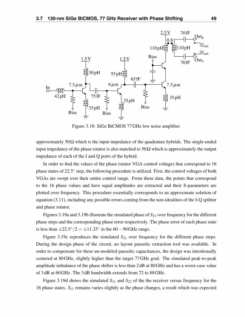
3.7 130-nm SiGe BiCMOS, 77 GHz Receiver with Phase Shifting 49
In
42pH
7.5 μm 7.5 μm
Bias
Bias BiasBias35pH
75fF
50pH
1.5V 1.5V
6 μm
55pH65fF
25pH35pH
2.5VOutp
Outn70fF
70fF
110pH 110pH
0.8
Zout
Zout
Figure 3.18: SiGe BiCMOS 77GHz low noise amplifier.
approximately 50Ω which is the input impedance of the quadrature hybrids. The single-ended
input impedance of the phase rotator is also matched to 50Ω which is approximately the output
impedance of each of the I and Q ports of the hybrid.
In order to find the values of the phase rotator VGA control voltages that correspond to 16
phase states of 22.5◦ step, the following procedure is utilized. First, the control voltages of both
VGAs are swept over their entire control range. From these data, the points that correspond
to the 16 phase values and have equal amplitudes are extracted and their S-parameters are
plotted over frequency. This procedure essentially corresponds to an approximate solution of
equation (3.11), including any possible errors coming from the non-idealities of the I-Q splitter
and phase rotator.
Figures 3.19a and 3.19b illustrate the simulated phase of S21 over frequency for the different
phase steps and the corresponding phase error respectively. The phase error of each phase state
is less than ±22.5◦/2 =±11.25◦ in the 60−90GHz range.
Figure 3.19c reproduces the simulated S21 over frequency for the different phase steps.
During the design phase of the circuit, no layout parasitic extraction tool was available. In
order to compensate for these un-modeled parasitic capacitances, the design was intentionally
centered at 80GHz, slightly higher than the target 77GHz goal. The simulated peak-to-peak
amplitude imbalance of the phase shifter is less than 2dB at 80GHz and has a worst-case value
of 3dB at 60GHz. The 3dB bandwidth extends from 72 to 88GHz.
Figure 3.19d shows the simulated S11 and S22 of the the receiver versus frequency for the
16 phase states. S11 remains varies slightly as the phase changes, a result which was expected
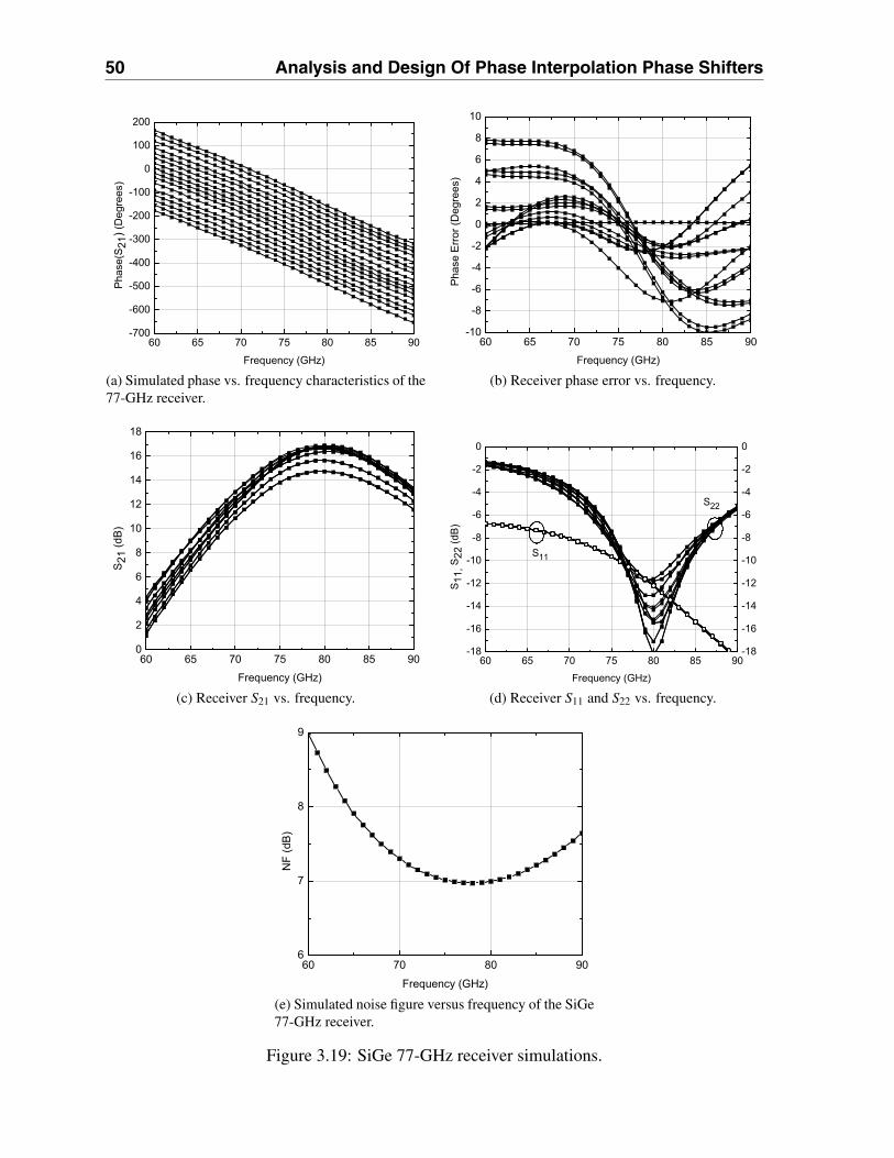
50 Analysis and Design Of Phase Interpolation Phase Shifters
(a) Simulated phase vs. frequency characteristics of the77-GHz receiver.
(b) Receiver phase error vs. frequency.
(c) Receiver S21 vs. frequency. (d) Receiver S11 and S22 vs. frequency.
(e) Simulated noise figure versus frequency of the SiGe77-GHz receiver.
Figure 3.19: SiGe 77-GHz receiver simulations.

3.8 65-nm CMOS, 94 GHz Transmitter with Phase Shifting 51
Out
PAPhase
Rotator
All-PassPolyphase
FilterIn
InputBuffer
IQBuffers
Figure 3.20: CMOS 94GHz transmitter.
due to the high reverse isolation of the LNA. Nevertheless, its value is −12dB at 80GHz which
is relatively poor for the case of low noise receivers. The reason for this design inconsistency
was the fact that the value of the input pad capacitance was overestimated and the inductor at
the input of the LNA was larger than it should have been. The output reflection coefficient S22
varies from −12dB to −18dB at 80GHz. However, the bandwidth over which S22 is better
than −10dB is relatively narrow.
Figure 3.19e illustrates the simulated noise figure of the receiver versus frequency of the
receiver. Although this simulation is generally unreliable because of the lack of modeling
of noise correlation in the transistor model [42], it provides an estimate of the noise figure,
typically a few dB higher than the expected measured one.
3.8. 65-nm CMOS, 94 GHz Transmitter with Phase Shifting
The block diagram of the 65-nm CMOS, 94 GHz transmitter is illustrated in figure 3.20.
The input signal under phase shift is first amplified by a two stage cascode buffer shown in
figure 3.21a. The buffer, apart from amplifying the input signal, provides input matching to
50Ω and output matching to 75Ω which is the input resistance of the following all-pass poly-
phase filter (presented in section 3.4.1).
The input buffer utilizes the topology discussed in [43] and features input shunt-series
transformer feedback matching to 50Ω. The output transformer, apart from matching to 75Ω,
it facilitates single-ended-to-differential conversion. It consumes a total of 16mA from 1.2V
power supply.
In order to assure constant 75Ω loading of the all-pass polyphase filter, differential buffers
were inserted between its output and the input of the phase rotator. The schematic of the
differential buffers is shown in figure 3.21a, where a cascode topology was preferred due to its
increased reversed isolation. This isolation is highly desirable since it shields the filter from
any input impedance variation that might occur in the phase rotator. The 75Ω input matching
network is formed by employing series-series inductive feedback, formed by the two 85pH and
90pH inductors. 130pH series peaking inductors are inserted between the common source and

52 Analysis and Design Of Phase Interpolation Phase Shifters
In
70pH
BiasBias
35pH
20 μm
20 μm
140pH
70pH
65fF
40 μm
40 μm
40pH
80pH 80pH0.7
Outp
Outn
0.6
1.2V1.2V
(a) CMOS 94GHz input buffer
In
85pH
85pH
16 μm16 μm
16 μm16 μm
130pH130pH
Bias
Bias
500fF
Out
72pH72pH
44fF
44fF
90pH90pH
1.2V
(b) CMOS 94GHz cascode IQ buffer
Figure 3.21: Input and differential buffers utilized in the transmitter.
common base transistors in order to increase the gain. The output matching network is formed
by the 72pH shunt inductors and 44fF series capacitors. Each differential buffer consumes
10mA from 1.2V power supply.
After the buffered polyphase filter, the phase rotator, which was presented in section 3.6.1,
completes the phase interpolation and generates the desired phase shift. The phase shifted
signal is then fed to a 4-stage medium-power power amplifier shown in figure 3.22. The power
amplifier was presented in [44] and features two input cascode stages followed by an AC-
coupled cascode stage that maximizes the signal swing at the output node. To ensure reliable
operation, the final common-gate stage is implemented with a low-power (LP) transistor, which
has a thicker gate oxide than the general purpose (GP) MOSFETs used elsewhere, making it
more immune to degradation due to large voltage swings. The power amplifier draws 65mA
from 1.2V power supply. It was measured as a separate breakout and exhibits small signal gain
of 7dB at 90GHz and a saturated output power of +3dBm.
A similar simulation methodology as in the 77GHz receiver was followed for the 94GHz
CMOS transmitter. Figures 3.23a and 3.23b illustrate the simulated phase of S21 over frequency
for the different phase steps and the corresponding phase error respectively. The phase error of
each state remains below ±11.25◦ in the 86−97GHz range.
Figure 3.23c reproduces the simulated S21 over frequency for the different phase steps. The
design was purposefully centered at 90GHz instead of 94GHz since the layout parasitic extrac-
tor provided with the technology tends to overestimate the parasitic capacitances in MOSFETs.

3.8 65-nm CMOS, 94 GHz Transmitter with Phase Shifting 53
In
60pH
Bias
Bias
BiasBias70pH
24 μm
24 μm
140pH
60pH
44fF
40 μm
40 μm
80pH
60pH
128fF
60pH
60 μm
20pH 128fF 60pH
80 μm
40pH 83fF
Out
1.2V1.2V
1.2V1.2V
Figure 3.22: CMOS 94GHz power amplifier.
This usually results in a design being centered slightly higher than simulated. The measure-
ment capabilities with the available VNA extend up to 94GHz and had the design ended up
higher than 94GHz, measurements at peak gain would have been impossible. The peak-to-peak
amplitude imbalance is 3dB at 90GHz while the peak gain is 16dB.
Finally, figure 3.23d shows the simulated reflection coefficients S11 and S22 over frequency
for the different phases. Due to the reverse isolation provided by the input buffer and power am-
plifier, any variation of the phase rotator impedance does not affect the reflection coefficients.
Both simulated S11 and S22 remain below −10dB between 90 and 100GHz.

54 Analysis and Design Of Phase Interpolation Phase Shifters
(a) Simulated phase vs. frequency characteristics of the94-GHz transmitter.
(b) Transmitter phase error vs. frequency.
(c) Transmitter S21 vs. frequency. (d) Transmitter S11 and S22 vs. frequency.
(e) Simulated input-output power characteristics of thetransmitter at 94GHz.
Figure 3.23: CMOS 94-GHz transmitter simulations.

4 Characterization
4.1. 77 GHz Receiver with Phase Shifting
The 77GHz receiver was fabricated in STMicroelectronics’ BiCMOS9MW process. The
die photo is illustrated in figure 4.1. The circuit occupies 660× 690 μm2 including the pads
and 150×500 μm2 without pads. The layout configuration was purposefully arranged so that
the circuit has a narrow and long shape. This configuration would be necessary in order to
vertically stack several of these receivers and add their outputs to form a phased-array. The
total measured power consumption is 128mW from 1.5V and 2.5V power supplies.
First, On-wafer S-parameter measurements were carried out in the 55−94GHz range using
a Wiltron 360B Vector Network Analyzer (VNA) and 110-GHz Cascade Infinity probes. The
LRRM (Line-Reflect-Reflect-Match) calibration method was used in order to correct the non-
idealities of the VNA and the 110GHz setup required to connect and probe the circuit. The
analog control voltages of the phase shifters were provided by an Agilent 4155 semiconductor
parameter analyzer, as shown in figure 4.2a.
The S-parameter measurement methodology was similar with the simulation methodology.
The control voltages of the variable gain amplifiers were swept over their entire range and S-
parameter measurements were conducted at each point. Then, the required phase states were
extracted. Figures 4.3a and 4.3b illustrate the measured phase and phase errors over frequency
when the phase is varied from 0◦ to 360◦ in sixteen 22.5◦ steps. Good agreement is observed
with the corresponding simulation results of figures 3.19a and 3.19b. The phase error remains
below 6◦ in the 72− 76GHz range and below 8◦ in the 70− 77GHz range which is the 3-dB
bandwidth of the entire receiver. Figure 4.3c shows the measured amplitude of S21 for the cor-
responding phase states. The maximum gain is 17dB with less than 2dB of peak-to-peak gain
imbalance. A shift of 6GHz in the center frequency of the receiver is observed compared with
simulation (figure 3.19c) as well as narrower 3dB bandwidth. Although the receiver was origi-
nally centered at higher frequency to account for possible shifts, the frequency shifted by 4GHz
55
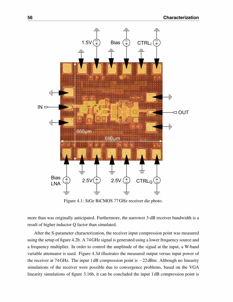
56 Characterization
INOUT
2.5V 2.5V CTRLQ
1.5V Bias CTRLI
BiasLNA
690μm660μm
Figure 4.1: SiGe BiCMOS 77GHz receiver die photo.
more than was originally anticipated. Furthermore, the narrower 3-dB receiver bandwidth is a
result of higher inductor Q factor than simulated.
After the S-parameter characterization, the receiver input compression point was measured
using the setup of figure 4.2b. A 74GHz signal is generated using a lower frequency source and
a frequency multiplier. In order to control the amplitude of the signal at the input, a W-band
variable attenuator is used. Figure 4.3d illustrates the measured output versus input power of
the receiver at 74GHz. The input 1dB compression point is −22dBm. Although no linearity
simulations of the receiver were possible due to convergence problems, based on the VGA
linearity simulations of figure 3.16b, it can be concluded the input 1dB compression point is

4.1 77 GHz Receiver with Phase Shifting 57
Wiltron 360BVector Network
Analyzer
Agilent 4155Semiconductor
Analyzer
(a) S-parameter measurement setup.
Agilent 4155Semiconductor
Analyzer
HP0-20GHzGenerator
X6W-bandMultiplier
W-bandVariable
AttenuatorW-bandPowerSensor
(b) Linearity measurement setup.
Agilent 4155Semiconductor
Analyzer
W-bandNoise
Source
W-bandVariable
Attenuator
Agilent W8486A Down-
converter
HP8970B NoiseFigure
Analyzer
(c) Noise figure measurement setup.
Figure 4.2: 77GHz receiver measurement setups.
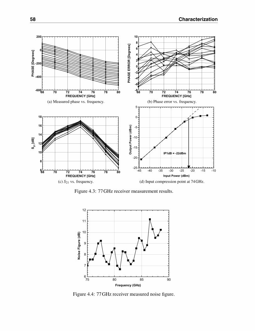
58 Characterization
68 70 72 74 76 78 80FREQUENCY [GHz]
-600
-400
-200
0
200PH
ASE
[Deg
rees
]
(a) Measured phase vs. frequency.
68 70 72 74 76 78 80FREQUENCY [GHz]
-8
-6
-4
-2
0
2
4
6
8
10
PHA
SE E
RR
OR
[Deg
rees
]
(b) Phase error vs. frequency.
68 70 72 74 76 78 80FREQUENCY [GHz]
6
8
10
12
14
16
18
S 21[d
B]
(c) S21 vs. frequency. (d) Input compression point at 74GHz.
Figure 4.3: 77GHz receiver measurement results.
Figure 4.4: 77GHz receiver measured noise figure.

4.2 94 GHz Transmitter with Phase Shifting 59
limited by the LNA linearity. In case a better compression point is required, which is likely the
case for radar receivers, gain control could be implemented in the LNA.
Finally, the noise figure of the receiver was measured using the setup of figure 4.2c. An
ELVA W-band noise source was used to provide the input to the receiver while an external
downconverter and noise figure analyzer where connected to the output. Noise figure measure-
ments in the 75− 87.5GHz are possible with this setup. Figure 4.4 illustrates the measured
noise figure of the receiver in this range. Its minimum value is 7dB which is in good agree-
ment with simulation.
Table 4.1 below summarizes the measured performance of the 77GHz receiver.
Measured Simulated
Gain 17dB 17dB3dB Bandwidth 7GHz (70−77GHz) 16GHz (72−88GHz)
Phase Shift 0◦ −360◦ (22.5◦ steps) 0◦ −360◦ (22.5◦ steps)RMS phase error @ 3dB BW < 4◦ < 3.5◦p-p phase error @ 3dB BW < 8◦ < 10◦
p-p phase error @ maximum gain 5◦ 6◦p-p gain error @ maximum gain 2dB 2dB
IP1dB −22dBm did not convergeNF 7dB 7dB
Table 4.1: Measured versus simulated performance of the 77GHz receiver.
4.2. 94 GHz Transmitter with Phase Shifting
The 94GHz transmitter was fabricated in STMicroelectronics’ 65 nm CMOS process. The
transmitter was part of a larger chip as shown in figure 4.5 where the output of the power
amplifier is connected to a pad through a λ/4 SPTD switch [45]. The complete transmit chain
consumes 142mW from 1.2V supply while occupying 800×150 μm2.
In order to conduct S-parameter measurements, the input and output are connected to the
Wiltron VNA while the analog controls to the Agilent 4155 semiconductor parameter analyzer.
The controls of the SPDT switch and the digital controls of the phase shifter are loaded to an
on-chip shift register through a pattern generator. Figure 4.6a illustrates the measured phase
versus frequency while figure 4.6b shows the phase error over frequency of the transmitter for
the 16 different phase states. The phase error reaches a minimum of 4◦ at 90GHz, at the center
of the PA bandwidth. Good agreement with the corresponding simulations of figures 3.23a
and 3.23b is observed.
Figure 4.6c illustrates the amplitudes of S21, S11 and S22 over frequency for the different
phases. A maximum small-signal gain of 3.8dB is demonstrated, with a maximum peak-to-

60 Characterization
OUT
IN
800μm
150μm
Figure 4.5: 65nm CMOS 94GHz transmitter die photo.
peak gain variation among all states of less than 4dB, at 90GHz. Compared with the simulated
S21 of figure 3.23c, the center frequency of S21 is at exactly the same frequency. However, the
gain is approximately 10dB lower and the amplitude imbalance slightly higher. This relatively
large inconsistency between measurement and simulated S21 has been a subject of extensive in-
vestigation by the author. Different simulation models were tested along with different extrac-
tion methods for parasitics with limited success in reproducing the measured gain reduction.
Furthermore, several different measurement techniques were attempted under various condi-
tions. What was observed is that the measured gain increased significantly when the power
supply was raised to values higher than 1.2V. Although this is case with every CMOS circuit
that utilizes cascodes from 1.2V, it may also be an indication of a layout inconsistency that
causes an IR drop in the on-chip power supply distribution. This is especially true since the
transmitter is a part of a more complicated chip in which designing a supply distribution has
been extraordinarily difficult.

4.2 94 GHz Transmitter with Phase Shifting 61
80 82 84 86 88 90 92 94FREQUENCY [GHz]
-400
-200
0
200
PHA
SE [D
egre
es]
(a) Transmitter measured phase vs. frequency.
80 82 84 86 88 90 92 94FREQUENCY [GHz]
-6-4-202468
101214
PHA
SE E
RR
OR
[Deg
rees
]
(b) Transmitter measured phase error vs. frequency.
80 82 84 86 88 90 92 94FREQUENCY [GHz]
-14
-12
-10
-8
-6
-4
-2
0
2
4
S 21, S
11 &
S22
[dB
]
S21
S22S11
(c) Transmitter measured S21 vs. frequency.
Figure 4.6: 94GHz transmitter measurement results.

62 Characterization
Measured Simulated
Gain 3.8dB 16dB3dB Bandwidth 28GHz (82−106?GHz) 14GHz (82−96GHz)
Phase Shift 0◦ −360◦ (22.5◦ steps) 0◦ −360◦ (22.5◦ steps)RMS phase error @ 3dB BW < 5◦ < 5.3◦p-p phase error @ 3dB BW < 12◦ < 11.5◦
p-p phase error @ maximum gain 4.5◦ 4◦p-p gain error @ maximum gain 4dB 3dB
PSAT (PA only) 3dBm 4dBm
Table 4.2: Measured versus simulated performance of the 94GHz transmitter.
Frequency Gain Phase Arrangement Phase Error Gain Error Reference
34GHz 11dB 0◦ −360◦, 16 steps 7◦ RMS 3dB [18]24GHz −11.3dB 0◦ −360◦ - 2.4dB [21]12GHz 3.5dB 0◦ −360◦, 16 steps 5.5◦ RMS 1dB [19]20GHz −4.6dB 0◦ −360◦, 16 steps 6.5◦ RMS 1.1dB RMS [36]60GHz −5.5dB 0◦ −180◦ - 3.3dB [46]60GHz −2dB 0◦ −360◦ 3◦ RMS - [46]60GHz −9.4dB 0◦ −180◦, 8 steps 9.2◦ RMS 6.2 [47]77GHz −19.2dB 0◦ −360◦, 16 steps 11◦ RMS 7.4dB [48]74GHz 17dB 0◦ −360◦, 16 steps 4◦ RMS 2dB This work90GHz 3.8dB 0◦ −360◦, 16 steps 5◦ RMS 4dB This work
Table 4.3: Comparison of different phase shifters.
The output power of the transmitter was measured with a similar setup as the one described
in figure 4.3d. However, due to the unavailability of a signal source with high output power at
90GHz, it was impossible to drive the transmitter into compression and determine the OP1dB
and PSAT .
Table 4.2 below summarizes the measured performance of the 94GHz transmitter.
4.3. Comparison with Relevant Work
Table 4.3 provides a comparison of different phase shifters. Although this comparison is not
absolute since the phase shifters are at different frequencies and target different applications,
it provides a summary of the phase and amplitude errors achieved by different phase shifters
found in the literature. Furthermore, it illustrates that the results presented in this work are of
equal performance or even better than lower frequency phase shifters.

5 Conclusion
In this thesis, different phase shifter architectures were investigated and their potential for
realization in IC form and operation in mm-wave frequencies was assessed. Although many
phase shifter topologies have been proposed during the last 60 years, only a handful of them
are capable to satisfy both requirements. The phase interpolation phase shifter was found to be
the best candidate due to its compact size, its ability to have gain and generate phase shifts in
the 0◦ −360◦ range.
Two circuits are required to realize the phase interpolation phase shifters: An I-Q splitter
and a variable gain amplifier. Extensive bibliographic studies were also conducted in order to
pick the proper topologies for both building blocks. Furthermore, two different I-Q splitters
and variable gain amplifiers were implemented in two different IC processes. The theoretical
analysis of the interpolation phase shifter revealed that the variable gain amplifiers need to have
as constant phase shift as possible when their gain varies. Variable gain amplifiers that satisfy
this requirement have not been extensively studied in the literature.
5.1. Contributions
The first CMOS phase shifter operating above 60GHz has been presented in this thesis. A
transmitter with phase shifting capabilities was also developed by utilizing the phase shifter.
The transmitter was able to generate phase shifts of 0◦ − 360◦ in 22.5◦ steps. Although this
transmitter was developed in October 2007, to the best of the author’s knowledge, no other
CMOS or SiGe BiCMOS phase shifter in the same frequency range has been reported up to
this date.
A 77GHz SiGe BiCMOS receiver has also been developed. There have been other 77GHz
phase shifters published prior to this receiver, the proposed receiver was the first to utilize phase
shifting in the RF front-end and as a result, the first to show calibrated VNA 0◦ − 360◦ phase
shift in this frequency range.
In the circuit design level, two novel phase rotator topologies have been proposed. First,
63

64 Conclusion
a 65nm CMOS rotator that facilitates both coarse digital phase control with respect to the se-
lected quadrant and analog fine control within the quadrant. Second, a SiGe BiCMOS rotator
based on MOS-HBT cascode variable gain amplifiers and exhibits improved phase stability
and linearity due to the constant current through the MOS transconductors. Moveover, the fea-
sibility of a compact, low-loss 3dB quadrature hybrid at W-band frequencies was proven. The
hybrid offers significantly reduced size than its transmission line counterparts while exhibiting
very broadband characteristics.
5.2. Future Work
The phase shifters presented in this thesis operate in an analog (or semi-analog) fashion and
require extraction of the phase shift states during measurements because of possible component
variations. Moreover, in a practical phased array system, there are several other sources of
error, as illustrated in figure 5.1 [49]. Most of the error sources, such as antenna coupling, are
out of the control of the circuit designer. As a result, calibration of the array is required [49].
This calibration procedure would also require an external mm-wave source in case the coupling
between the antennas, line lengths and air interface are considered, which can be a costly and
time consuming procedure.
Figure 5.1: Errors in phased array systems.
Future research could focus on the development of a calibration procedure that would avoid
the use of an external source. A two step procedure, utilizing on-chip loopback through cou-
plers or SPDT switches, and off-chip loopback through a reflector could be developed.

5.3 Publication 65
5.3. Publication
The results of this thesis were published in the IEEE RFIC 2009 Symposium [50].

66 Conclusion

Bibliography
[1] H. P. Forstner, H. Knapp, H. Jager, E. Kolmhofer, J. Platz, F. Starzer, M. Treml,
A. Schinko, G. Birschkus, J. Bock, K. Aufinger, R. Lachner, T. Meister, H. Schafer,
D. Lukashevich, S. Boguth, A. Fischer, F. Reininger, L. Maurer, J. Minichshofer, and
D. Steinbuch, “A 77GHz 4-channel automotive radar transceiver in SiGe,” in Radio Fre-
quency Integrated Circuits Symposium, 2008. RFIC 2008. IEEE, Atlanta, GA, Jun. 17–
Apr. 2008, 2008, pp. 233–236.
[2] J. M. Gilbert, C. H. Doan, S. Emami, and C. B. Shung, “A 4-Gbps Uncompressed Wire-
less HD A/V Transceiver Chipset,” IEEE Micro, vol. 28, no. 2, pp. 56–64, Mar./Apr.
2008.
[3] M. Skolnik, Introduction to Radar Systems. McGraw-Hill, 2002.
[4] K.-J. Koh, J. May, and G. Rebeiz, “A Millimeter-Wave (40-45 GHz) 16-Element Phased-
Array Transmitter in 0.18-μm SiGe BiCMOS Technology,” IEEE Journal of Solid-State
Circuits, vol. 44, no. 5, pp. 1498–1509, May 2009.
[5] A. Babakhani, X. Guan, A. Komijani, A. Natarajan, and A. Hajimiri, “A 77-GHz Phased-
array Transceiver With On-chip Antennas in Silicon: Receiver and Antennas,” Solid-State
Circuits, IEEE Journal of, vol. 41, no. 12, pp. 2795–2806, Dec. 2006.
[6] R. J. Mailloux, Phased Array Antenna Handbook, 2nd ed. Artech House, 2005.
[7] C. A. Balanis, Antenna Theory: Analysis and Design, 3rd ed. Wiley, 2005.
[8] S. T. Nicolson, K. H. K. Yau, S. Pruvost, V. Danelon, P. Chevalier, P. Garcia, A. Chantre,
B. Sautreuil, and S. P. Voinigescu, “A low-voltage SiGe BiCMOS 77-GHz automotive
radar chipset,” IEEE Transactions on Microwave Theory and Techniques, vol. 56, pp.
1092–1104, May 2008.
67
68 Bibliography
[9] G. Avenier, S. P. Voinigescu, N. Revil, P. Chevalier, S. Pruvost, J. Bouvier, G. Troil-
lard, L. Depoyan, M. Buczko, S. Montusclat, A. Margain, S. T. Nicolson, K. H. K. Yau,
D. Gloria, A. Chantre, M. Diop, N. Loubet, N. Derrier, C. Leyris, S. Boret, and D. Du-
tartre, “0.13 μm SiGe BiCMOS Technology Fully Dedicated to mm-wave Applications,”
IEEE Journal of Solid-State Circuits, vol. 44, no. 9, pp. 2312–2321, Sep. 2009.
[10] T. O. Dickson, K. H. K. Yau, T. Chalvatzis, A. M. Mangan, E. Laskin, R. Beerkens,
P. Westergaard, M. Tazlauanu, M.-T. Yang, and S. P. Voinigescu, “The Invariance of
Characteristic Current Densities in Nanoscale MOSFETs and Its Impact on Algorithmic
Design Methodologies and Design Porting of Si(Ge) (Bi)CMOS High-speed Building
Blocks,” Solid-State Circuits, IEEE Journal of, vol. 41, no. 8, pp. 1830–1845, Aug. 2006.
[11] S. P. Voinigescu, RF and High-Speed ICs Course Notes. University of Toronto, 2008.
[12] T. O. Dickson, M. A. LaCroix, S. Boret, D. Gloria, R. Beerkens, and S. P. Voinigescu, “30-
100-GHz inductors and transformers for millimeter-wave (Bi)CMOS integrated circuits,”
IEEE Transactions on Microwave Theory and Techniques, vol. 53, no. 1, pp. 123–133,
Jan. 2005.
[13] J. White, “High Power, p-i-n Diode Controlled, Microwave Transmission Phase Shifters,”
IEEE Transactions on Microwave Theory and Techniques, vol. 13, no. 2, pp. 233–242,
Mar 1965.
[14] ——, “Diode phase shifters for array antennas,” IEEE Transactions on Microwave Theory
and Techniques, vol. 22, no. 6, pp. 658–674, Jun 1974.
[15] ——, “Review of semiconductor microwave phase shifters,” Proceedings of the IEEE,
vol. 56, no. 11, pp. 1924–1931, Nov. 1968.
[16] R. Garver, “Broad-band diode phase shifters,” IEEE Transactions on Microwave Theory
and Techniques, vol. 20, no. 5, pp. 314–323, May 1972.
[17] S. K. Koul and B. Bhat, Microwave and Millimeter Wave Phase Shifters. Artech House,
1991.
[18] B.-W. Min and G. Rebeiz, “Single-Ended and Differential Ka-Band BiCMOS Phased
Array Front-Ends,” IEEE Journal of Solid-State Circuits, vol. 43, no. 10, pp. 2239–2250,
Oct. 2008.
[19] D.-W. Kang and S. Hong, “A 4-bit cmos phase shifter using distributed active switches,”
IEEE Transactions on Microwave Theory and Techniques, vol. 55, no. 7, pp. 1476–1483,
July 2007.

Bibliography 69
[20] F. Ellinger, R. Vogt, and W. Bachtold, “Compact reflective-type phase-shifter MMIC for
C-band using a lumped-element coupler,” IEEE Transactions on Microwave Theory and
Techniques, vol. 49, no. 5, pp. 913–917, May 2001.
[21] J.-C. Wu, C.-C. Chang, S.-F. Chang, and T.-Y. Chin, “A 24-GHz full-360◦ CMOS
reflection-type phase shifter MMIC with low loss-variation,” in Proc. IEEE Radio Fre-
quency Integrated Circuits Symposium (RFIC), 2008, April 2008, pp. 365–368.
[22] T. Hancock and G. Rebeiz, “A 12-GHz SiGe phase shifter with integrated LNA,” IEEE
Transactions on Microwave Theory and Techniques, vol. 53, no. 3, pp. 977–983, March
2005.
[23] A. Nagra and R. York, “Distributed analog phase shifters with low insertion loss,” IEEE
Transactions on Microwave Theory and Techniques, vol. 47, no. 9, pp. 1705–1711, Sep
1999.
[24] C. Tsironis and P. Harrop, “Dual gate GaAs MESFET phase shifter with gain at 12 GHz,”
Electronics Letters, vol. 16, no. 14, pp. 553–554, 3 1980.
[25] M. Kumar, R. Menna, and H.-C. Huang, “Broad-Band Active Phase Shifter Using Dual-
Gate MESFET,” IEEE Transactions on Microwave Theory and Techniques, vol. 29,
no. 10, pp. 1098–1102, Oct 1981.
[26] A. Abidi, “Direct-conversion radio transceivers for digital communications,” IEEE Jour-
nal of Solid-State Circuits, vol. 30, no. 12, pp. 1399–1410, Dec 1995.
[27] B. Razavi, “Design considerations for direct-conversion receivers,” IEEE Transactions
on Circuits and Systems II: Analog and Digital Signal Processing, vol. 44, no. 6, pp.
428–435, Jun 1997.
[28] A. Tarighat, R. Bagheri, and A. Sayed, “Compensation schemes and performance analysis
of IQ imbalances in OFDM receivers,” IEEE Transactions on Signal Processing, vol. 53,
no. 8, pp. 3257–3268, Aug. 2005.
[29] E. Laskin, M. Khanpour, R. Aroca, K. W. Tang, P. Garcia, and S. P. Voinigescu, “A
95 GHz Receiver with Fundamental-frequency VCO and Static Frequency Divider in
65nm Digital CMOS,” in Solid-State Circuits Conference, 2008. ISSCC 2008. Digest of
Technical Papers. IEEE International, San Francisco, CA, Feb. 3–7, 2008, pp. 180–605.
[30] C. Lee, T. Yao, A. Mangan, K. Yau, M. A. Copeland, and S. P. Voinigescu, “SiGe BiC-
MOS 65-GHz BPSK transmitter and 30 to 122 GHz LC-varactor VCOs with up to 21%
70 Bibliography
tuning range,” 2004. IEEE Compound Semiconductor Integrated Circuit Symposium, pp.
179–182, Oct. 24–27, 2004.
[31] Y. Yu, P. Baltus, A. van Roermund, D. Jeurissen, A. de Graauw, E. van der Heijden,
and R. Pijper, “A 60 GHz digitally controlled phase shifter in CMOS,” in 34th European
Solid-State Circuits Conference, 2008. ESSCIRC 2008, Sept. 2008, pp. 250–253.
[32] M. Morton, J. Comeau, J. Cressler, M. Mitchell, and J. Papapolymerou, “5 bit, silicon-
based, X-band phase shifter using a hybrid Π / T high-pass/low-pass topology,” Mi-
crowaves, Antennas & Propagation, IET, vol. 2, no. 1, pp. 19–22, February 2008.
[33] D. M. Pozar, Microwave Engineering, 3rd ed. Wiley, 2005.
[34] B. Razavi, RF Microelectronics, 1st ed. Prentice Hall, 1999.
[35] T. H. Lee, The Design of CMOS Radio-Frequency Integrated Circuits, 2nd ed. Cam-
bridge University Press, 2003.
[36] K.-J. Koh and G. M. Rebeiz, “0.13μm CMOS Phase Shifters for X-, Ku-, and K-band
Phased Arrays,” IEEE Journal of Solid-State Circuits, vol. 42, no. 11, pp. 2535–2546,
Nov. 2007.
[37] R. C. Frye, S. Kapur, and R. C. Melville, “A 2-GHz quadrature hybrid implemented in
CMOS technology,” IEEE Journal of Solid-State Circuits, vol. 38, no. 3, pp. 550–555,
Mar. 2003.
[38] F. Ali and A. Podell, “Design and applications of a 3:1 bandwidth GaAs monolithic spiral
quadrature hybrid,” in Gallium Arsenide Integrated Circuit (GaAs IC) Symposium, 1990.
Technical Digest 1990., 12th Annual, New Orleans, LA, Oct. 7–10, 1990, pp. 279–282.
[39] W. M. C. Sansen and R. G. Meyer, “Distortion in bipolar transistor variable-gain ampli-
fiers,” IEEE J. Solid-State Circuits, vol. 8, no. 4, pp. 275–282, Aug. 1973.
[40] C.-C. Hsu and J.-T. Wu, “A highly linear 125-MHz CMOS switched-resistor
programmable-gain amplifier,” IEEE Journal of Solid-State Circuits, vol. 38, no. 10, pp.
1663–1670, Oct. 2003.
[41] T. O. Dickson, R. Beerkens, and S. P. Voinigescu, “A 2.5-V, 40-Gb/s decision circuit
using SiGe BiCMOS logic,” in VLSI Circuits, 2004. Digest of Technical Papers. 2004
Symposium on, Jun. 17–19, 2004, pp. 206–209.

Bibliography 71
[42] K. H. K. Yau and S. P. Voinigescu, “Modeling and extraction of SiGe HBT noise parame-
ters from measured y-parameters and accounting for noise correlation,” in Silicon Mono-
lithic Integrated Circuits in RF Systems, 2006. Digest of Papers. 2006 Topical Meeting
on, San Diego, CA, Jan. 18–20, 2006.
[43] M. Khanpour, K. W. Tang, P. Garcia, and S. P. Voinigescu, “A Wideband W-band Re-
ceiver Front-end in 65-nm CMOS,” Solid-State Circuits, IEEE Journal of, vol. 43, no. 8,
pp. 1717–1730, Aug. 2008.
[44] E. Laskin, M. Khanpour, S. T. Nicolson, A. Tomkins, P. Garcia, A. Cathelin, D. Belot,
and S. P. Voinigescu, “Nanoscale CMOS Transceiver Design in the 90–170-GHz Range,”
IEEE Transactions on Microwave Theory and Techniques, vol. 57, pp. 3477–3490, Dec.
2009.
[45] A. Tomkins, P. Garcia, and S. P. Voinigescu, “A 94 GHz SPST Switch in 65nm Bulk
CMOS,” in Compound Semiconductor Integrated Circuits Symposium, 2008. CSICS ’08.
IEEE, Monterey, CA, Oct. 12–15, 2008, pp. 1–4.
[46] M.-D. Tsai and A. Natarajan, “60 GHz passive and active RF-path phase shifters in
silicon,” in Radio Frequency Integrated Circuits Symposium, 2009. RFIC 2009. IEEE,
Boston, MA, Jun. 7–9, 2009, pp. 223–226.
[47] Y. Yu, P. Baltus, A. van Roermund, D. Jeurissen, A. de Graauw, E. van der Heijden, and
R. Pijper, “A 60 GHz digitally controlled phase shifter in CMOS,” in Solid-State Circuits
Conference, 2008. ESSCIRC 2008. 34th European, Edinburgh, Sep. 15–19, 2008, pp.
250–253.
[48] S. Y. Kim and G. M. Rebeiz, “A 4-bit Passive Phase Shifter for Automotive Radar Appli-
cations in 0.13 μm CMOS,” in Compound Semiconductor Integrated Circuit Symposium,
2009. CISC 2009. Annual IEEE, Greensboro, NC, Oct. 11–14, 2009, pp. 1–4.
[49] C. T. Charles and D. J. Allstot, “A Calibrated Phase and Amplitude Control System for a
1.9 GHz Phased-array Transmitter Element,” IEEE Transactions on Circuits and Systems
I: Regular Papers, vol. 56, no. 12, pp. 2728–2737, Dec. 2009.
[50] I. Sarkas, M. Khanpour, A. Tomkins, P. Chevalier, P. Garcia, and S. P. Voinigescu, “W-
band 65-nm CMOS and SiGe BiCMOS transmitter and receiver with lumped I-Q phase
shifters,” in Radio Frequency Integrated Circuits Symposium, 2009. RFIC 2009. IEEE,
Boston, MA, Jun. 7–9, 2009, pp. 441–444.


![Liquid Crystal Based Dielectric Waveguide Phase Shifters ... · tems (MEMS) are available as possible solutions for DW phase shifters. In [5] and [6] high impedance surfaces (HIS)](https://img.pdfslide.us/doc/110x75/5f6580af6a466a36f634975b/liquid-crystal-based-dielectric-waveguide-phase-shifters-tems-mems-are-available.jpg)


![CPW band-stop filter using unloaded and loaded EBG … papers...band-stop filters, low-pass filter and band-pass filter [2, 3], phase shifters [4], and antennas [5]. Examples of](https://img.pdfslide.us/doc/110x75/6043774997ca054282461acf/cpw-band-stop-ilter-using-unloaded-and-loaded-ebg-papers-band-stop-ilters.jpg)