Embed Size (px)
Citation preview
Sensors & Transducers, Vol. 156, Issue 9, September 2013, pp. 276-285
276
SSSeeennnsssooorrrsss &&& TTTrrraaannnsssddduuuccceeerrrsss
© 2013 by IFSAhttp://www.sensorsportal.com
The Design of an Embedded Video Data
Acquisition System
1 Chongyu Wei, 2 Weichen Wei, 1 Zuping Gu 1 Qingdao University of Science & Technology, No.99 Songling road, Qingdao, 266061, P. R.China
2 Melbourne University, VIC, Australia 1 Tel.& fax: 86-532-88959036, E-mail: [email protected]
Received: 5 June 2013 /Accepted: 25 August 2013 /Published: 25 September 2013 Abstract: A video transmission system generally consists of three main parts: A video data acquisition unit, transmission networks and play back terminals. The video data acquisition unit is one of the main parts. This paper focuses on an embedded video data acquisition hardware and software design. In the design, a PXA310 is used as a primary processor. The software design is based on an Android operating system. First, the paper briefly introduces the hardware design including overall scheme and the selection of key components. Then, the software design of the video data acquisition unit is introduced more detail, which includes the transplant of an Android operating system and the application software implementations for video data acquisition and processing. The modifications of BLOB boot program, the modifications of the operating system kernel and the NAND FLASH driver transplantation are described in more detail. The description of the video data acquisition software design includes the use of the Android internal class “Mediarecorder”, the method of extracting frame data according to 3GP and H.264 protocol, and the use of the socket interface to transmit frame data to a 3G wireless network called TD-SCDMA. The designed acquisition unit has been tested in a video surveillance and monitoring system and the experiment results are given at the end of the paper. Copyright © 2013 IFSA. Keywords: Networking video monitoring, Android, System transplant, Video data acquisition, H.264, Transmission unit.
1. Introduction In recent years, the increasing market demands
for network surveillance camera systems provide a good chance for the video data acquisition, processing and transmission technology development. And with the rapid increase in market penetration of 3G wireless cellular networks and their transmission bandwidths, wireless video surveillance and monitoring system can be deployed where a 3G network deployed. Under this condition, surveillance camera systems based on wireless networks and Internet becomes the mainstream of the monitoring
system [1, 2]. On the other hand, wireless video surveillance is also one of the main driving forces for 3G market development and will be an important growth of future mobile applications. Broadband wireless networks and the development of video compression coding techniques provided the necessary conditions for promotion of wireless video surveillance technology. In developing the surveillance camera systems above, how to design the unit for video data acquisition, processing and coding, and transmissions through a wireless network or Internet is a pivotal work, and have been becoming a hot point in technology development [12-15].
Article number P_1357
Sensors & Transducers, Vol. 156, Issue 9, September 2013, pp. 276-285
277
Video transmission based on the embedded system technology has features of low cost, compact size, easy to create and flexible applications. Android [3] is widely used embedded operating systems with open source code in recent years. Developing a video data acquisition and transmission unit based on an embedded system technology and for use in a 3G network is of great significance.
This paper describes the hardware and software design of the video data acquisition and processing.
2. Hardware Design of The Video Data Acquisition, Processing and Transmission Unit
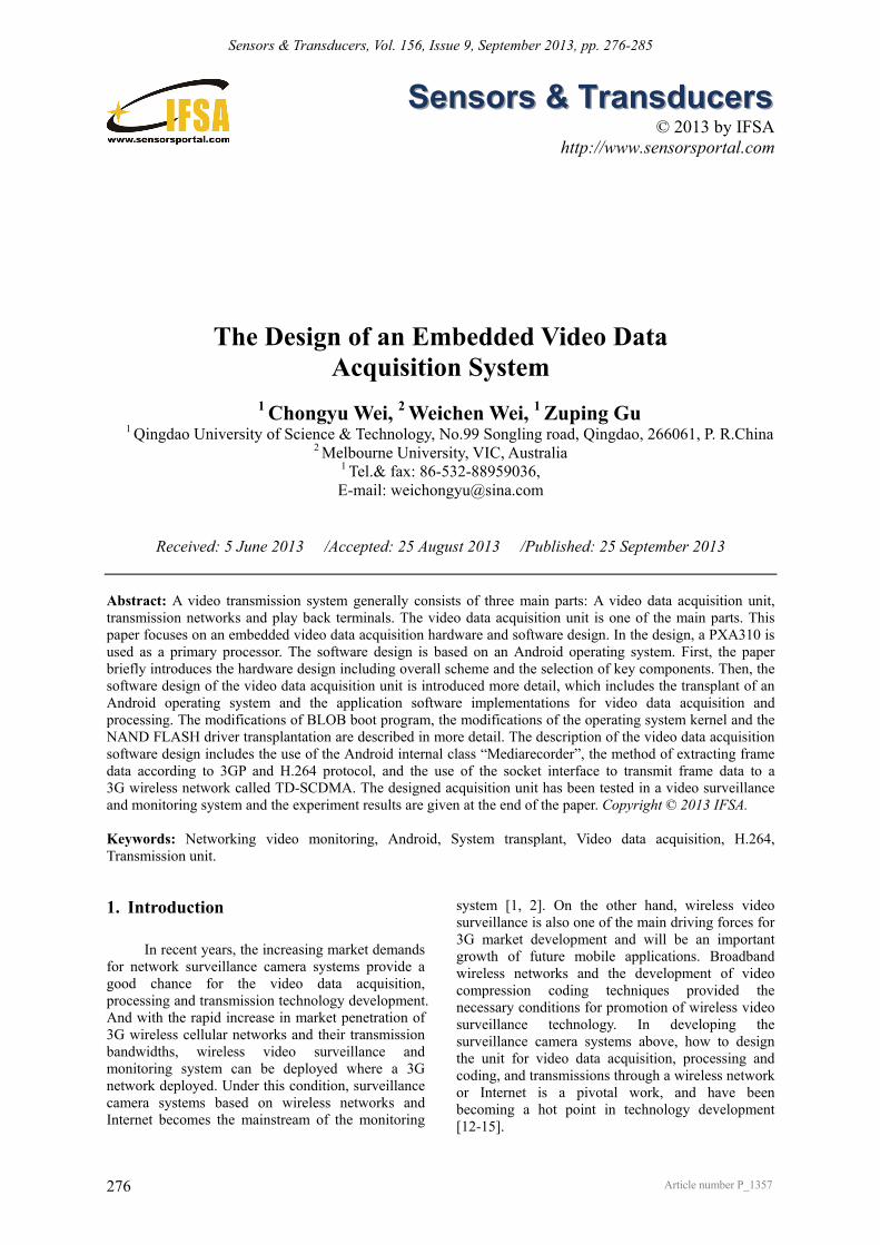
The hardware platform mainly consists of a
camera unit on the front end, a PXA310 [4, 5] processor module and a TM1902 wireless modem, as shown in Fig. 1. The Video camera OV7670 is an image sensor with 8 bits resolution data output and its frame rate is 30 F/s. The TM1902 modem supports TD-SCDMA HSUPA wireless transmissions. The Android platform is selected as the operating system.
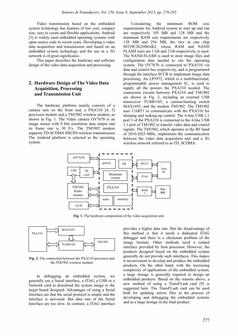
Considering the minimum ROM size requirements for Android system to start up and run are respectively 105 MB and 128 MB and the minimum RAM size requirements are respectively 128 MB and 256 MB, the two in one chip MT29C2G24MAKJ, whose RAM and NAND FLASH sizes are 1 Gb and 2 Gb respectively, is used. The NAND-FLASH is used to store image files and configuration data needed to run the operating system. The OV7670 is connected to PXA310 via data and control bus respectively, and is programmed through the interface SCCB to implement image data processing. An LP3972, which is a multifunctional, programmable power management IC, is used to supply all the powers the PXA310 needed. The connection circuits between PXA310 and TM1902 are shown in Fig. 2, including an external USB transceiver TUSB1105, a current-limiting switch MAX1693, and the modem TM1902. The TM1902 uses UART1 to communicate with the PXA310 for sleeping and waking-up control. The 6-line USB 1.1 port 3 of the PXA310 is connected to the 4-line USB 1.1 port of TM1902 to transfer video data and control signals. The TM1902, which operates in the RF band of 2010-2025 MHz, implements the communication between the video data acquisition unit and a 3G wireless network referred to as TD_SCDMA.
UIM
TM1902 Radio
modem
PXA310
reset
power clk
memory
Minimumsystem
LCD
TF card
OV7670
RS485
Pan &tilt
RS232
JTAG
Host PC
Fig. 1. The hardware composition of the video acquisition unit.
Fig. 2. The connection between the PXA310 processor and
the TM1902 wireless modem
In debugging an embedded system, we generally use a Serial interface, a JTAG, a USB or a Network card to download the system image to the target board designed. Advantages of using a Serial Interface are that the serial protocol is simple and the interface is universal. But data rate of the Serial Interface are too slow. In contrast, a JTAG interface
provides a higher data rate. But the disadvantage of this method is that it needs a dedicated JTAG debugger and there is a checksum problem of the image formats. Other methods need a related interface provided by host processor. However, the products designed based on the embedded system generally do not provide such interfaces. This makes it inconvenient to develop and produce the embedded products. On the other hand, with the increasing complexity of applications of the embedded system, a large storage is generally required in design an embedded products. Based on the reasons above, a new method of using a TransFLash card [9] is suggested here. The TransFLash card can be used both for updating mirror files in the process of developing and debugging the embedded systems and as a large storage in the final product.
PXA310
TM1902
MAX1693
TUSB1105
Sensors & Transducers, Vol. 156, Issue 9, September 2013, pp. 276-285
278
3. Software Design 3.1. General Software Solution
Software development requires first transplant
Android operating system [6-8] to the embedded hardware platform. And then implement the software design for the video data acquisition, encoding, extracting video frame data, and transferring the encoded video data into the 3G wireless network. The transplantation of the Android system includes the modification of the boot loader, the Linux kernel and the root file system.
There are two implementation schemes for video data acquisition and processing. The first one is to directly encode video data from the inner CAMERA class of Android. Disadvantages of this software encoding approach are that it takes a lot of processor resources and its output frame rate is generally lower. The second one is the use of the MEDIARECORDER class of Android for video data acquisition and encoding. Since the outputs of the MEDIARECORDER class are the documents in 3GP or MP4 format, they must be transformed into the video data stream for streaming media transmission. This is a hardware encoding approach that does not require the transplantation of code library. Therefore it is easy for implementing and can output a higher frame rate. To output a suitable frame rate, the second method is adopted in the paper. Camera resolution and encode format are configured in the MEDIARECORDER class. The encoded data are packed in file stream of 3GP format. The data for each frame are picked up from the file stream according to the 3GP protocol. Then the frame data picked up is sent to the server via the wireless modem TM1902.
For sending video data through the TM1902 modem, operations needed include dialing wireless TD-SCDMA network, establishing PPP protocol connection and sending video data by an application program calling the Socket interface [10]. Android 2.3 and later versions include a software module supporting TD-SCDMA modems and what needed in achieving above operations is to add TM1902 to the module and configure it accordingly.
The OV7670 camera used has a photosensitive array of 640 × 480. Maximum frame rate can be 30 f/s when outputting VGA video data with CIF image format and H.264 coding standard. UDP datagram fashion is used for video data transmission and TCP for signaling. Since the maximum transmission unit (MTU) in link layer is 1500 bytes, and considering the total length of IP and UDP datagram heads is 28 bytes, the maximum UDP length in a local area network is 1472 bytes and 576 bytes in Internet. The maximum transmission unit for UDP transferring is 548 bytes.
3.2. Transplanting Android Operating System
3.2.1. General Description
There are many kinds of bootloaders in use. Considering the PXA310 Board Development Kit has contained a BLOB, the transplantation of the bootloader in the article is based on the BLOB given.
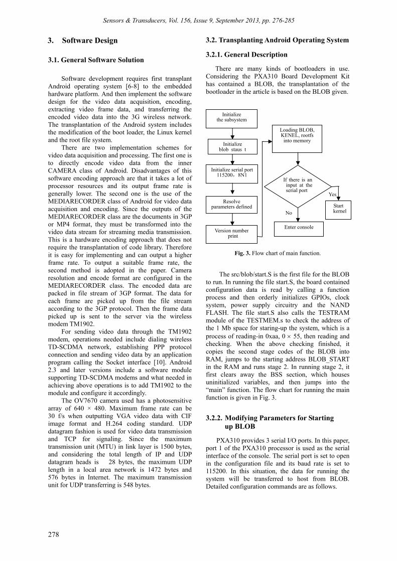
Fig. 3. Flow chart of main function.
The src/blob/start.S is the first file for the BLOB to run. In running the file start.S, the board contained configuration data is read by calling a function process and then orderly initializes GPIOs, clock system, power supply circuitry and the NAND FLASH. The file start.S also calls the TESTRAM module of the TESTMEM.s to check the address of the 1 Mb space for staring-up the system, which is a process of reading-in 0xaa, 0 55, then reading and checking. When the above checking finished, it copies the second stage codes of the BLOB into RAM, jumps to the starting address BLOB_START in the RAM and runs stage 2. In running stage 2, it first clears away the BSS section, which houses uninitialized variables, and then jumps into the “main” function. The flow chart for running the main function is given in Fig. 3.
3.2.2. Modifying Parameters for Starting up BLOB
PXA310 provides 3 serial I/O ports. In this paper, port 1 of the PXA310 processor is used as the serial interface of the console. The serial port is set to open in the configuration file and its baud rate is set to 115200. In this situation, the data for running the system will be transferred to host from BLOB. Detailed configuration commands are as follows.
No
Yes
Initializethe subsystem
Initializeblob staus t
Initialize serial port115200,8N1
Resolveparameters defined
Version number print
Loading BLOB, KENEL, rootfs into memory
If there is an input at the serial port
Enter console
Start kernel

Sensors & Transducers, Vol. 156, Issue 9, September 2013, pp. 276-285
279
/* Use STUART */ #define USE_SERIAL1 1 #define TERMINAL_SPEED baud_115200
In booting the kernel to start up, it must be insure that all the modules on the hardware platform have been enabled and clocked properly. Since the enable pins of modules connect the processor’s GPIOs, in the BLOB the GPIOs should be set to the response level or MFP pins. These settings include camera enable pin, the write-protect pin of the NAND FLASH, the power supply pin of the power manager, and the pins for enabling and clocking TM1902.
It requires BLOB read the kernel image files exactly from NAND FLASH, which implies that the kernel address must be obtained accurately, for booting the system kernel to start up normally. Therefore, the BLOB should be partitioned in light of the image file sizes, and their initial addresses should be marked. Generally, the BLOB is partitioned from address 0, and in the order of BLOB, kernel, Android root file system. The partition sizes are in the image file sizes rounding. Detailed setting commands are as follows.
/* and where do they live in flash */ #define BLOB_FLASH_BASE (0x00000000) #define BLOB_FLASH_LEN (1024* 1024) #define PARAM_FLASH_BASE (BLOB_FLASH_BASE + BLOB_FLASH_LEN) #define PARAM_FLASH_LEN (0) /* no parameters */ #define KERNEL_FLASH_BASE (PARAM_ FLASH_BASE + PARAM_FLASH_LEN) #define KERNEL_FLASH_LEN(3*1024*1024) #define LOAD_RAMDISK 0/* load ramdisk into ram */ #define RAMDISK_FLASH_BASE (KERNEL_ FLASH_BASE+ KERNEL_FLASH_LEN) #define RAMDISK_FLASH_LEN (96*1024* 1024) #define USERDATA_FLASH_BASE (RAMDISK_FLASH_BASE + RAMDISK_FLASH_LEN) #define USERDATA_FLASH_LEN (32 * 1024 * 1024)
3.3. Transplanting the System Kernel
Transplanting the kernel is modifying and recompiling the kernel to run corresponding hardware platform, which requires add driver programs and other kernel modules to support corresponding new chips and hardware modules on the platform. The main contents of the kernel
transplantation include modifying the kernel booting parameters and adding new device driver programs.
Equipment driver programs are the interfaces between the operating system kernel and platform hardware devices. The driver programs implement functions of initializing or releasing devices, transferring data from kernel to hardware devices or vice versa, reading the data that an application program sends to a device file or responding the data it asking for, detecting device faults and implementing fault-tolerance.
In the operating system Linux, there are mainly three kinds of device files. They are block devices, character devices and network equipments. Jobs of writing device driver programs mainly include the writing of sub functions and putting them into different “file_operations” fields.
3.3.1. Transplanting the Driver of NAND FLASH
Since the login of an NAND FLASH proceeds its
driver, when the NAND driver logs it will match all the devices logged on the bus by matching their names. If the matching is successful, it will execute the probe function of the NAND driver, namely pxa3xx_nand_probe(), which is the beginning of running the NAND driver program. Logical flow chart is given in Fig. 4.
Initialize NAND
controller
Scann NAND and
match devices
Add MTD partition
Fig. 4. Structure diagram of NAND Flash driver.
1). Initializing the NAND controller. On starting up, the system will allocate the NAND controller a data structure, in which the configuring data are included such as a controller’s clock, a reference address, and the transferring mode. Android system kernel can support various NAND chips. During initializing, the controller can read the ID of the NAND chip by operating a register and match it to the ID in configuration. This operation will continue until the controller finds the chip’s configuration data and then completes the controller initialization. Fig. 5 gives the initialization flow chart.
Source codes for the configuration of MT29C2G24MAKJ are as follows.
struct type_info[] = {
…… { DFC_FLASH_Toshiba2GbX16, &toshiba2GbX16}, { DFC_FLASH_Micron_2Gb_X_16, µn2GbX16}, { DFC_FLASH_NULL, NULL},
};

Sensors & Transducers, Vol. 156, Issue 9, September 2013, pp. 276-285
280
struct dfc_flash_info micron2GbX16 = {
.timing = { .tCH = 10, /* tCH, Enable signal hold time */ .tCS = 35, /* tCS, Enable signal setup time */ .tWH = 15, /* tWH, ND_nWE high duration */ .tWP = 25, /* tWP, ND_nWE pulse time */ .tRH = 15, /* tRH, ND_nRE high duration */ .tRP = 25, /* tRP, ND_nRE pulse width */ /* tR = tR+tRR+tWB+1, ND_nWE high to ND_nRE low for read */ .tR = 25000, /* tWHR, ND_nWE high to ND_nRE low delay for status read */ .tWHR = 60, .tAR = 10, /* tAR, ND_ALE low to ND_nRE low delay */ }, .enable_arbiter = 1,/* Data flash bus arbiter enable */ .page_per_block = 64, /* Pages per block */ .row_addr_start = 1, /* Second cycle start, Row address start position */ .read_id_bytes = 4, /* Returned ID bytes */
… …
No
Yes
Configure controller
Start
The chip ID= ith configuration ID ?
Read chip ID
End
Configure controller
Fig. 5. Flow chart of NAND controller initialization.
2). The function for scanning NAND. This function is used to print device ID in starting up kernel and lookup bad blocks in the NAND and setup a bad block table (BBT), by which the kernel can judge if a data block is normal or not and then complete device scanning.
3). Add MTD subarea information. By using the function “mtd_part”, an original MTD device can be divided into several parts and logged in “mtd_table”. In the “mtd_table” each original MTD partition can be logged as a MTD device. Two functions of
“add_mtd_device” and “add_mtd_partitions” are used to do this work. Detail codes are as follows.
littleton_nand_info.parts = pxa300_android_128m_partitions; littleton_nand_info.nr_parts = ARRAY_SIZE(pxa300_android_128m_partitions); add_mtd_partitions(monahans_mtd, pdata->parts, pdata->nr_parts);
3.3.2. Compiling Kernel Source Codes
This work contains the following steps. 1) Decompressing kernel. Decompress kernel
source codes to the host working environment. In this paper, the kernel version used is Linux-2.6.29 and compressing format is tar.gz. Use “#tar zxvf linux-2.6.29.tar.gz” to decompress the kernel to the working directory.
2) Configuring the kernel to support ARM platform. The kernel source codes include the source codes supporting x86 and ARM system. The source codes supporting ARM platform are in the “arch/arm” directory. In compiling, setup the corresponding infrastructure and cross compile tool chain at the top layer of the “Makefile”, which makes calling the file “arch/arm/Kconfig” as configuring Linux kernel. Commands used are as follows.
#ARCH ?= $(SUBARCH) #CROSS_COMPILE ?= ARCH=arm CROSS_COMPILE=arm-eabi-
3) Modifying platform clock rate. Modify the line 42 of the file “arch/arm/mach-pxa/pxa3xx.c” in kernel and set the clock rate to 13 MHz, which is the external clock signal frequency of PXA310 processor. Commands are as follows.
/* Crystal clock: 13MHz */ #define BASE_CLK 13000000
4) Making kernel configuration file. For the kernel used in the paper, when installing a patch package a default configuration file “pxa3xx_android_defconfig” will be added in the directory of the configuration file “arch/arm/configs”. The hardware platform in the paper uses this default configuration. Executing command “#make menuconfig”, the PC screen will display a man-machine interface in Fig. 6. On completing kernel configuration and executing command “#cp .config arch/arm/configs/myconfig”, the current configuration files will be stored.
5) Adding hardware platform ID. When BLOB starts system kernel, it first transfers the platform ID stored in the register R1 to the kernel. If the ID has not been added in the kernel, kernel starts up fault. Therefore, the processor ID must be added in the kernel before starting up. The ID of PXA310 is 1388. The codes for adding platform ID are as follows.

Sensors & Transducers, Vol. 156, Issue 9, September 2013, pp. 276-285
281
Where the command “machine_is_xxx” is a function used to judge if the current platform is right, “CONFIG_xxxx” is a function produced during the kernel configuration, “MACH_TYPE_xxx” is the definition of the system platform ID, and “number” is the platform ID value.
Fig. 6. Printed screen of kernel configuration.
#machine_is_xxx CONFIG_xxxx MACH_TYPE_xxx number littleton MACH_LITTLETON
LITTLETON 1388
6) Modifying MTD partition. The operation of the kernel is based on the MTD partition. The BLOB and kernel must be partitioned in full accord, including partition name, size, starting address. The MTD information of the kernel is as follow.
static struct mtd_partition pxa300_android_128m_partitions[] = { [0] = { .name = "Bootloader", .offset = 0, .size = 0x100000, .mask_flags = MTD_WRITEABLE, /* force read-only */ }, [1] = { .name = "Kernel", .offset = 0x100000, .size = 0x300000, .mask_flags = MTD_WRITEABLE, /* force read-only */ }, [2] = { .name = "system", .offset = 0x0400000, .size = 0x4000000, /* mount 64M fs */ }, [3] = { .name = "userdata", .offset = 0x4400000, .size = 0x2000000, }, …… },
When above modifications completed, the kernel can be compiled. To do this, execute command “#make zImage” and the kernel image named “zImage” will be formed under the “arch/arm/boot” directory. Using a TF card to download [9] and in combining with BLOB command, the kernel image can be burned to the hardware platform, i.e. the target board.
4. Software Implementation of the Video Data Acquisition Front End Based on Android
Video and audio data capturing and processing
are implemented by using the “Mediarecorder” class of Android platform. The “Mediarecorder” is based on the “OpenCore” library and achieved in JNI by calling "media_jni" library file [11]. Image resolution, coding standard and output file type can be set directly in the “Mediarecorder” class. Fig. 7 gives the operation flow chart.
Configuring parameters for the operation of the camera
Setting coding format and resolution
Setting output path
Call “prepare” of mediarecorder
Starting up mediarecorder, recording
Fig. 7. Mediarecorder configuration flow chart.
The “Mediarecorder” calls “setCamera” to select a camera, “setVideoSource” to capture video data from the camera, and “setOutputFormat” to set output routing path, which must be a file descriptor. The detailed “Mediarecorder” configurations are as follows.
mediarecorder.setCamera(c); mediarecorder.setVideoSource(MediaRecorder.VideoSource.CAMERA); mediarecorder.setOutputFormat(MediaRecorder.OutputFormat.THREE_GPP); mediarecorder.setVideoEncoder(MediaRecorder.VideoEncoder.H264); mediarecorder.setVideoFrameRate(15); mediarecorder.setVideoSize(640, 480);
Because the “Mediarecorder” class can only
record local video data, another class called

Sensors & Transducers, Vol. 156, Issue 9, September 2013, pp. 276-285
282
“LocalSocket” is required for sending the coded video data to network server via socket interface and UDP protocol. The flow chart is shown in Fig. 8.
Fig. 8. Logical connection of LocalSocket.
The detailed codes of the “LocalSocket” are as follows.
LocalServerSocket mVideoLocalServerSocket = null; LocalSocket mVideoLocalClientSocket = null; LocalSocket mVideoReceiveSocket = null; mVideoLocalServerSocket = new LocalServerSocket("Video"); mVideoReceiveSocket.connect(new LocalSocketAddress("Video")); mVideoReceiveSocket.setReceiveBufferSize(500000); mVideoReceiveSocket.setSendBufferSize(500000); mVideoLocalClientSocket = mVideoLocalServerSocket.accept(); mVideoLocalClientSocket.setReceiveBufferSize(500000); mVideoLocalClientSocket.setSendBufferSize(500000);
The output data of the “Mediarecorder” are file
streams in 3GP format. Since no writing back, the file stream can’t be played in stream media; neither the stream server can recognize the files and transfer them. The recorded video data must be further processed to pick up their frame data in H.264 format.
The recorded H.264 data are stored in a media package from which the frame data can be picked up according to the H.264 protocol. The H.264 data are stored in the sequence of NAL cells. Namely a NAL cell stores a frame. Generally there are two fashions for packaging the H.264 data. One is that the first four bytes of each frame is its head 0x00000001 [3]. The other one is that the first four bytes of each frame is its length instead of head. The latter is used in Android “Mediarecorder” outputs. Therefore, in
processing the recorded file stream in 3GP format, first check the “mov” (movie package) in the 3GP file stream and pick up decoding parameters SPS and PPS, add H.264 frame head to the two parameters respectively to form data frames, and send these two data frames to the stream media server. Then, find the media data package “madt”, read the first four bytes of the “NAL”, calculate their length, read the NAL according to the length calculated. Afterwards, repeat the above operations in circulation till the processing is finished. Flow chart for above processing is shown in Fig. 9.
Fig. 9. Flow chart of extracting frames.
The TM1902 is used as a modem transceiver to connect the 3G network TD-SCDMA. The modem is controlled by PXA310 via programmed AT commands. Since data interface of TM1902 is a USB, the USB driver must be transplanted to operate the modem. On the other hand, since the current kernel supports PPP dialing, the Android system can use RIL (Radio Interface Layer) to control the modem. The modem driver is the function “usbserial.ko” for changing the USB interface into a serial port. After loaded the “usbserial.ko”, a node called “ttyUSB*”, which is used as a channel for transmitting AT commands, will be produced.
1). In the file “reference_ril.c” of the RIL, there are several operations for using AT commands. These operations must be modified corresponding to different hardware platform, which can be done via the “onRequest” interface. Modify the function “at_open” in “ril/reference-ril/atchannel.c” to open the channel “ttyUSB0” for modem TM 1902. Detailed source codes are as follows.
int fd2 = -1; while(fd2 < 0) { fd2 = open ("/dev/ttyUSB0", O_RDWR); if (fd2 < 0) {
No
Yes
Start
Initializing cache
Lookup “moov” and “mdat”
Recording ?
End
Reading data according to the length given above, storing the data in the cache and setting a 4 bytes offset
Setting the first 4 bytes of the cache as a frame head
Reading the first 4 bytes of data in the cache and write back its length
Mediarecorder outputing
Local client socket
Local server socket
Local receiver socket
Socket transmiting

Sensors & Transducers, Vol. 156, Issue 9, September 2013, pp. 276-285
283
perror ("opening URC interface. retrying..."); sleep(10); }
The modifications in “ril/reference-ril/reference-ril.c” are that delete command “#define PPP_TTY_PATH "/ dev/omap_csmi_tty1"” and add command “#define PPP_TTY_PATH "/dev/ppp0"”. 2). Add an access point in the file “apn-conf-sdk.xml”. For mobile network TD-SCDMA, the access point is 46007. Source codes for doing this are as follows.
<apn carrier="CHINA MOBILE" mcc="460" mnc="07" apn="cmnet" user="*" server="*" password="*" mmsc="null" />
3). Modify the file “init.rc” and add “pppd_gprs”
as system server. Source codes for doing this are as follows.
service ril-daemon /system/bin/rild -l libreference-ril.so -- -d /dev/ttyUSB0 socket rild stream 660 root radio socket rild-debug stream 660 radio system user root group radio cache inet misc service pppd_gprs /etc/ppp/init.gprs-pppd /dev/ttyUSB0 user root group radio cache inet misc disabled
On above modifications finished, Android
system can control TM1902 to dial TD-CDMA network and make PPP connection. The Socket requests from application layer will be translated by RIL layer into corresponding AT commands and sent to the hardware at bottom layer. The flow chart for video data acquisition, processing and sending into TD-SCDMA network is shown in Fig. 10.
5. Test Results 5.1. The Transplantation of Android
Platform
In debugging an embedded system, a serial interface is generally used to connect the target board and a host PC. The host uses serial tools such as HyperTerminal to display debugging information. JTAG port is used to download BLOB to the target board. If command lines are displayed on host screen,
it means that the BLOB starts successfully. Since parameters for starting BLOB have been modified and the TF card driver has been transplanted, further adding a download command “tfdownload” is needed. The commands for reading the TF card, downloading and burning the system image are as follows.
Fig. 10. Flow chart of video data acquisition and processing unit.
blob>tfdownload init //initializing TF card [9] blob>nanderase -z 0x100000 0x300000 //brushing NAND blob> tfdownload zImage //downloading system image blob>nandwrite -z 0x80800000 0x100000 <zImage-actual-length> //burning image blob>nanderase -y 0x400000 0x4000000 blob> tfdownload system blob>nandwrite -y 0x80800000 0x400000 <system.img actual length> blob>nanderase -y 0x4400000 0x2000000 blob>tfdownload userdata blob>nandwrite -y 0x80800000 0x4400000 <userdata.img actual length>
The debugging output information printed on
host screen is shown in Fig. 11, which implies that the BLOB starts up successfully and the initialization of the TF card has been completed.
After the BLOB started up, the software has been in a suitable situation for system operation. At this time the operating system will jump to the kernel entry address 0x80800000, and start the kernel. Fig. 12 gives the starting information and the command line parameters of Linux-2.6.29 system.
Upon starting up, the kernel will check peripheral equipments such as NAND FLASH. If it
Yes
No
Start
Connecting localsocket & socket
Startup video recording thread
Set parameters for mediarecorder
Startup mediarecorder
Capturing SPS & PPS and sending
Read and calculate the length of NAL
Read the data of the NAL
Send via socket
Stop recording ?
End
Sensors & Transducers, Vol. 156, Issue 9, September 2013, pp. 276-285
284
can’t identify the NAND, the kernel can’t start up normally. The information displayed in Fig. 13 shows that the kernel reads the ID of the NAND equipment as 0xba2c, which is the chip MT29C2G24MAKJ used in this paper. The following data are the information read from MTD partition table.
The Linux kernel will eventually mounts Android file system of YAFFS format and runs the “Init” process in the file system. The “Init” process starts other local processes and services. The above start-up processes can be printed by adding a debugging command “Logcat” in the kernel, see Fig. 14.
5.2. The Running Results of the Video Acquisition Software.
By using the debugging command “Logcat”, the
information for running the video data acquisition software can also be seen on host screen. Fig. 15 gives the running results. In the figure, D/ and I/ are debugging information types denoting "debugging" and "notice" respectively. “VIDEOINF” is the software name. The debugging information shows that this program is acquiring video data.
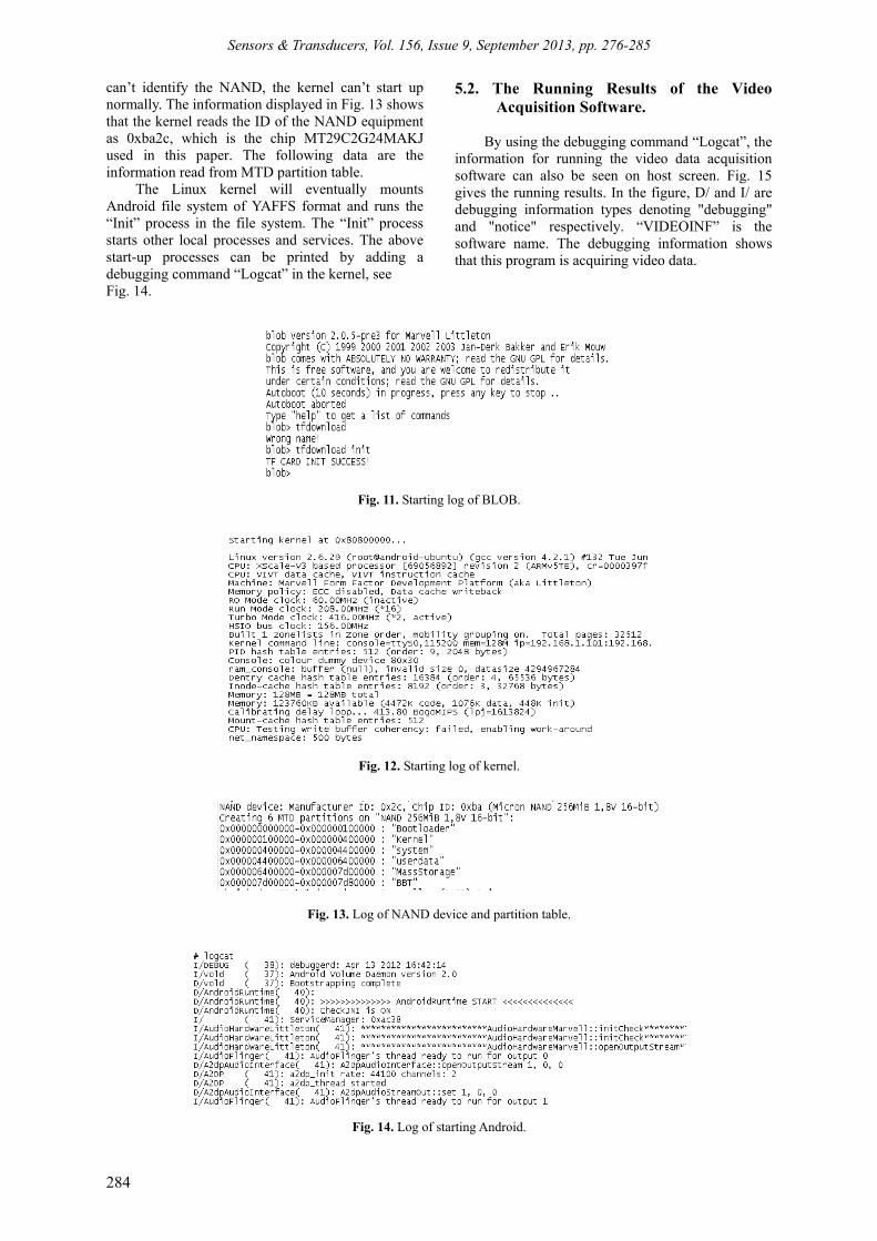
Fig. 11. Starting log of BLOB.
Fig. 12. Starting log of kernel.
Fig. 13. Log of NAND device and partition table.
Fig. 14. Log of starting Android.
Sensors & Transducers, Vol. 156, Issue 9, September 2013, pp. 276-285
285
Fig. 15. Log of the VIDEOINF.
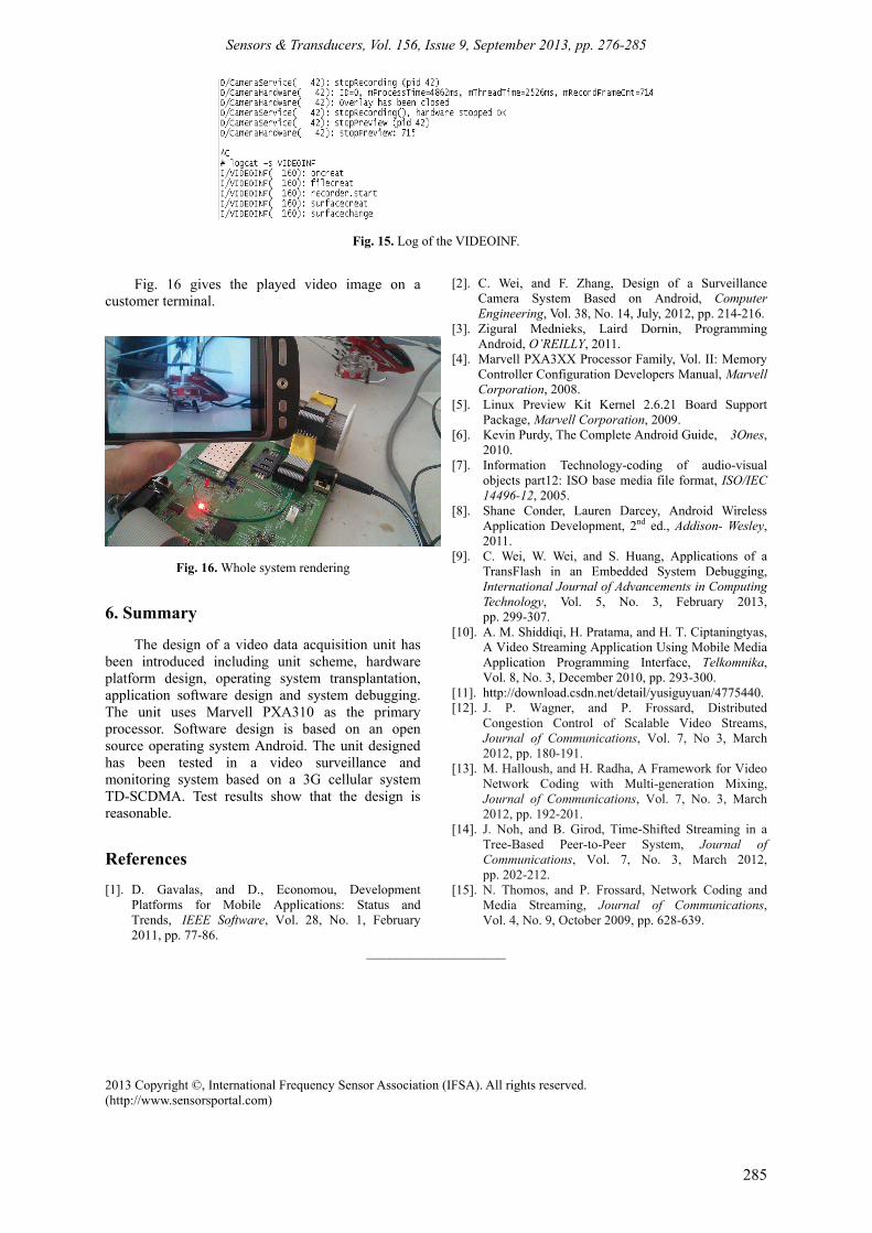
Fig. 16 gives the played video image on a customer terminal.
Fig. 16. Whole system rendering
6. Summary
The design of a video data acquisition unit has been introduced including unit scheme, hardware platform design, operating system transplantation, application software design and system debugging. The unit uses Marvell PXA310 as the primary processor. Software design is based on an open source operating system Android. The unit designed has been tested in a video surveillance and monitoring system based on a 3G cellular system TD-SCDMA. Test results show that the design is reasonable.
References [1]. D. Gavalas, and D., Economou, Development
Platforms for Mobile Applications: Status and Trends, IEEE Software, Vol. 28, No. 1, February 2011, pp. 77-86.
[2]. C. Wei, and F. Zhang, Design of a Surveillance Camera System Based on Android, Computer Engineering, Vol. 38, No. 14, July, 2012, pp. 214-216.
[3]. Zigural Mednieks, Laird Dornin, Programming Android, O’REILLY, 2011.
[4]. Marvell PXA3XX Processor Family, Vol. II: Memory Controller Configuration Developers Manual, Marvell Corporation, 2008.
[5]. Linux Preview Kit Kernel 2.6.21 Board Support Package, Marvell Corporation, 2009.
[6]. Kevin Purdy, The Complete Android Guide, 3Ones, 2010.
[7]. Information Technology-coding of audio-visual objects part12: ISO base media file format, ISO/IEC 14496-12, 2005.
[8]. Shane Conder, Lauren Darcey, Android Wireless Application Development, 2nd ed., Addison- Wesley, 2011.
[9]. C. Wei, W. Wei, and S. Huang, Applications of a TransFlash in an Embedded System Debugging, International Journal of Advancements in Computing Technology, Vol. 5, No. 3, February 2013, pp. 299-307.
[10]. A. M. Shiddiqi, H. Pratama, and H. T. Ciptaningtyas, A Video Streaming Application Using Mobile Media Application Programming Interface, Telkomnika, Vol. 8, No. 3, December 2010, pp. 293-300.
[11]. http://download.csdn.net/detail/yusiguyuan/4775440. [12]. J. P. Wagner, and P. Frossard, Distributed
Congestion Control of Scalable Video Streams, Journal of Communications, Vol. 7, No 3, March 2012, pp. 180-191.
[13]. M. Halloush, and H. Radha, A Framework for Video Network Coding with Multi-generation Mixing, Journal of Communications, Vol. 7, No. 3, March 2012, pp. 192-201.
[14]. J. Noh, and B. Girod, Time-Shifted Streaming in a Tree-Based Peer-to-Peer System, Journal of Communications, Vol. 7, No. 3, March 2012, pp. 202-212.
[15]. N. Thomos, and P. Frossard, Network Coding and Media Streaming, Journal of Communications, Vol. 4, No. 9, October 2009, pp. 628-639.
___________________
2013 Copyright ©, International Frequency Sensor Association (IFSA). All rights reserved. (http://www.sensorsportal.com)