Embed Size (px)
Citation preview

Embedded Wireless Data Acquisition System
Kalyanramu Vemishetty
Thesis Submitted to the Faculty of the
Virginia Polytechnic Institute and State University
in partial fulfillment of the requirements for the degree of
Master of Science
In
Mechanical Engineering
Alfred L. Wicks, Chairmen
Charles F. Reinholtz, Co-chairman
Craig Woolsey, Committee Member
February 23, 2005
Blacksburg, Virginia, USA, 2005
©Kalyanramu Vemishetty, 2005
Embedded Wireless Data Acquisition System
By
Kalyanramu Vemishetty
Abstract
The Wake Forest University Physiology/Pharmacology (WFU Phys./Pharm.) electrophysiology
research labs currently carry out memory research by recording neural signals from laboratory
animals tethered to nearby signal conditioning and recording equipment. A wireless neural signal
recording system is desirable because it removes the cumbersome wires from the animal, allowing it
to roam more freely. The result is an animal that is more able to behave as it would in its natural
habitat, thus opening the possibility of testing procedures that are not possible with wired recording
systems.
Sampling rates obtained by conventional RF wireless systems ten to be very low (800Hz) since the
bandwidth of these RF wireless systems is low. Also, interfacing methods (RS-232) to develop RF
systems are slow (57.6Kbps). Another shortcoming of RF systems is the high power consumption.
This thesis presents development of embedded wireless system to replace wired systems. RF wireless
system is developed to replace wired electrophysiology system. An infrared wireless system
development is discussed to achieve higher sampling rates unachievable by RF wireless system.
Infrared operate at data rates 4Mbps and high sampling rates can be achieved. Infrared systems are
interfaced using ISA interfacing technique and operate at faster rates (8Mbytes/sec). Also, Infrared
systems consume low power than RF systems. Power consumption is an important consideration as
application in hand is battery powered.

iii
Acknowledgements
I would like to thank my advisor Dr. Wicks for giving me the very special opportunity to work on my
Masters project. This project allowed me to develop solid understanding of wireless communications.
Thanks to John Bird for giving much appreciated electrical guidance.
I would like to thank my family. The emotional and financial support that they provided made my
transition from undergraduate student to graduate student much more comfortable than it might have
otherwise been.
Finally, I would like to give recognition to the friends that I made during my stay at Virginia Tech.
You made my time at Virginia Tech very enjoyable.
iv
Table of Contents
Chapter 1 INTRODUCTION................................................................................................................. 1
1.1 Motivation:................................................................................................................................... 1
1.1.1 Neurological Signals:............................................................................................................ 1
1.1.2 Memory Research ................................................................................................................. 2
1.2 Electrophysiology recording systems .......................................................................................... 4
1.2.1 Wired Electrophysiology Recording Systems ...................................................................... 4
1.3 Motivation for Wireless Electrophysiology System .................................................................... 5
1.4 Wireless Data acquisition – Radio Frequencies........................................................................... 5
1.5 Wireless Data acquisition – Infrared............................................................................................ 6
Chapter 2 BACKGROUND................................................................................................................... 7
2.1 Bluetooth...................................................................................................................................... 7
2.1.1 Avoiding Interference: Low Power....................................................................................... 8
2.1.2 Personal Area Networks........................................................................................................ 9
2.2 Frequency Hopping Technique.................................................................................................. 11
2.3 Interfacing to PC........................................................................................................................ 12
2.4 Infrared Data Transfer (IrDA).................................................................................................... 12
2.4.1 The IrDA Architecture ........................................................................................................ 14
2.4.2 The IrDA Physical Layer .................................................................................................... 16
2.4.3 The 4-Mbit/s Link ............................................................................................................... 17
2.4.4 Interfacing to PC ................................................................................................................. 20
2.4.5 Choice of Technology for application................................................................................. 21
Chapter 3 Embedded RF Wireless Data Acquisition System .............................................................. 22
3.1 Conceptual Model of the Embedded Wireless Transmission System: ...................................... 22
3.2 RF Data Acquisition System...................................................................................................... 23
3.3 PIC 18F452 ................................................................................................................................ 24
3.4 ML 2724 Starter Kit................................................................................................................... 25
3.5 Analog Section of the Data Acquisition System........................................................................ 26
3.6 Receive and Display components .............................................................................................. 26
Chapter 4 Components of RF Wireless Data Acquisition System....................................................... 30
4.1 PIC Microcontroller and C Program.......................................................................................... 30
4.1.1 UART Communication ....................................................................................................... 30
v
4.1.2 A/D Conversion................................................................................................................... 31
4.2 Data Memory and Program Memory ......................................................................................... 32
4.3 Functions .................................................................................................................................... 33
4.3.1 Overhead of Passing Variables............................................................................................ 33
4.3.2 Interrupts ............................................................................................................................. 34
4.4 C code......................................................................................................................................... 34
4.4.1 Initialization of UART Module ........................................................................................... 36
4.5 ML2724 Starter Kit .................................................................................................................... 40
Chapter 5 Performance of the RF Wireless Data Acquisition System ................................................. 42
5.1 Stanford Research Systems Function Generator ........................................................................ 42
5.2 PIC code testing.......................................................................................................................... 43
5.2.1 RF Wireless Data Acquisition System Testing ................................................................... 43
Chapter 6 Infrared Data Acquisition System........................................................................................ 45
6.1 Infrared System Design .............................................................................................................. 45
6.2 Infrared Receiving station .......................................................................................................... 46
6.3 LabVIEW Program..................................................................................................................... 48
6.3.1 IrDA Data Client: ................................................................................................................ 48
6.4 Selection of infrared chips for data transmission ....................................................................... 50
6.5 Basic Architectures..................................................................................................................... 51
6.6 ISA Overview............................................................................................................................. 51
6.7 Interface between infrared chip and microcontroller ................................................................. 52
6.8 The circuit layout........................................................................................................................ 53
6.9 Infrared Communication ............................................................................................................ 55
6.9.1 Configuration....................................................................................................................... 55
6.9.2 Checking the connection between Infrared Device and PIC Microcontroller..................... 57
6.10 Loop Back Test for Fast Infrared Communication................................................................... 58
Chapter 7 Conclusion ........................................................................................................................... 60

vi
List of Figures
Figure 1-1: Typical Neurological Signal Representation....................................................................... 2
Figure 1-2: Rat undergone surgery to access hippocamal neural signals .............................................. 3
Figure 1-3: Wired Electrophysiology system…………………………………………………………13
Figure 1-4: Shown is a rat in a testing box. ........................................................................................... 5
Figure 2-1: International Radio Frequency Band Allocation................................................................. 8
Figure 2-2: Frequency Hopping and Piconets........................................................................................ 9
Figure 2-3: Piconet in House ............................................................................................................... 10
Figure 2-4: Frequencies hopping with respect to time......................................................................... 12
Figure 2-5: Infrared Network............................................................................................................... 13
Figure 2-6: Viewing Angle specified in IrDA specification................................................................ 14
Figure 2-7: IrDA Protocol Stack.......................................................................................................... 15
Figure 2-8: 4-Mbits/sec Link Architecture .......................................................................................... 18
Figure 2-9: 4PPM Message Encoding ................................................................................................. 18
Figure 2-10: Signal –to-Noise Ratio gain and pulse width trade-off ................................................... 19
Figure 2-11: 4-Mbits/sec packet format............................................................................................... 20
Figure 3-1: Embedded Wireless Data Acquisition System Model ...................................................... 23
Figure 3-2: RF Data Acquisition system design .................................................................................. 23
Figure 3-3: RF Wireless Data Acquisition System with components and interfaces .......................... 24
Figure 3-4: PICDEM-2 Board with PIC18F452 .................................................................................. 24
Figure 3-5: Connection between ICD2 debugger, PICDEM-2 and PC ............................................... 25
Figure 3-6: ML 2724 Starter Kit from Micro Linear ........................................................................... 25
Figure 3-7: The ML2724 evaluation board is used to wirelessly communicate with the PIC. a. A
close-up of the Evaluation board. b. The evaluation board is connected to the PC through a serial
cable. The LabVIEW interface code is seen on the computer display................................................ 26
Figure 3-8: LabVIEW front panel showing received data ................................................................... 27
Figure 3-9: Message Packet encoded ML2724 Starter Kit .................................................................. 28
Figure 4-1: Flow chart explaining code on PIC18F452....................................................................... 35
Figure 4-2: Software buffer inside PIC microcontroller and its pointers............................................. 37
Figure 4-3: Components of ML2724 Transceiver Evaluation Board .................................................. 40
Figure 5-1: PICDEM-2 board with Function Generator input............................................................. 42

vii
Figure 5-2: Data collected using wireless RF Data Acquisition System.............................................. 43
Figure 5-3: The performance of the prototype (bottom) was compared to the performance of the wired
setup (top)............................................................................................................................................. 44
Figure 6-1: Infrared Data Acquisition System Model .......................................................................... 46
Figure 6-2: IrDA-USB Dongle from SigmaTel.................................................................................... 46
Figure 6-3: Infrared Dongle components ............................................................................................. 47
Figure 6-4: Windows message showing detection of other computer.................................................. 48
Figure 6-5: IrDA Data Server GUI for transmitting data through the infrared port on computer....... 48
Figure 6-6: (a) GUI for receiving data through infrared port on computer (IrDA Data Client)........... 50
Figure 6-7: Connections between PIC PCB board and ICD2 Debugger.............................................. 53
Figure 6-8: Schematics of PIC- ISA board........................................................................................... 54
Figure 6-9: Picture of Evaluation Board in ISA Slot............................................................................ 55
Figure 6-10: Infrared Communication Controller Components ........................................................... 57
Figure 6-11: IrDA FIR encoder inside FDC37C672............................................................................ 59

viii
List of Tables
Table 1: Comparison of Wireless technologies ................................................................................... 21
Table 2: Summary of AT Commands .................................................................................................. 41
Table 3: Logical Device number of devices inside FDC37C672......................................................... 56
Table 4: Device Identification registers inside FDC37C672 ............................................................... 58
Table 5: Device Identification registers of Infrared Block (IrCC 2.0) inside FDC37C672................. 58

1
Chapter 1
INTRODUCTION
This section is intended to give a brief introduction to the common data acquisition methods
of physiological signals. One of the main motivations for this project was to provide a replacement
for wired systems with wireless systems for collecting physiological signals. Wired and wireless
recording instrumentation used in the memory research are introduced, and the motivation for a
wireless system is explained in next section. One of the problems with wired system is that wired
systems place geometric constraints on the design of test boxes for collecting physiological signals
from rat’s brain. Also, off-animal electronics in wired systems degrade electrophysiological signals
by adding noise. Wireless systems will reduce problems associated with wired systems in memory
research. A comparison is made between wired and wireless techniques used for acquiring
physiological signals. Radio Frequency and Infrared wireless instrumentation is introduced, and the
motivation for the infrared wireless system is explained.
1.1 Motivation:
In physiological monitoring, scientists’ measure electrical signals from a variety of body
parts, including muscles, heart, lungs, brain, and optic nerves, to understand the part’s functions. All
body parts respond to electrical signals, and scientists acquire and analyze these responses and
electrical signals. This thesis will discuss an application of wireless technology for measuring
neurological signals from rat's brain. Electrical signals generated during brain’s thought process are
called neurological signals.
1.1.1 Neurological Signals:
Neurons are cells of the central and peripheral nervous system and they provide the pathways
to distribute brain’s electrical signals. Neurons transmit messages electrochemically. Due to the
neural firing, action potentials are generated. A typical neural signal is shown in Figure 1-1 below

2
Figure 1-1: Typical Neurological Signal Representation
To characterize this neurological signal in time domain, at least 10 samples are required from each
cycle. At least 10 samples are required from each cycle so as not to lose the amplitude information of
the neurological signal. To extract accurate information 20 samples are required from each cycle.
Each cycle is millisecond and it is divided into 20 points to extract accurate time domain information.
So, the sampling duration between each sample is sec20
10sec20
1 3−
=milli . The sampling rate
required to extract time domain information from the neurological signal is (inverse of 20
milliseconds) 20 KHz.
1.1.2 Memory Research
It has long been recognized that the part of the brain known as the hippocampus plays a part
in the brains ability to memorize [17]. For this reason, memory research is carried out by recording
neural electrical activity (neural signals) of the hippocampus and statistically correlating this activity
to memory. Researchers at Wake Forest University are currently involved in electrophysiological
memory research using laboratory rats.
In this research with laboratory rats, the animals are placed in a special testing box and are
taught certain tasks. The animals learn how to receive a reward, such as water, by memorizing what
actions to take based on visual cues. An automated electro-mechanical testing apparatus presents the

3
reward to the animal if the tasks are correctly completed. Once the animal has learned the task, it is
fitted with a special hat to make its hippocamal neural signals accessible. Firing patterns of the
hippocampal neurons are then recorded while the animal performs the learned task. The action-
potentials of the recorded neural signal are electronically isolated and an attempt is made to identify
the neural mechanisms responsible for memory.
To give researchers convenient long term access to the electrical signals generated by rat’s
neurons, the rat must be fitted with a special cap, often called a hat, which allows for a direct
electrical connection with the neural signals. Rats must undergo surgery to have a hat installed. To
start, the rats are given anesthesia that put them to sleep. The animals head is secured and the skull is
exposed. Small holes are drilled through the skull over the parts of the brain where an array of
electrodes is to be dropped into the soft brain tissue. During the surgery, a micromanipulator is used
to make fine adjustments to the depth of the electrodes in the brain, while an audio amplifier
amplifies the signal from the electrodes, allowing the surgeon to audibly verify the electrodes
proximity to firing hippocampal neurons. Once the array is in place, dental cement is used to
carefully seal the array to the skull. Figure 1-2 shows a picture of a rat that has had a hat installed.
Figure 1-2: Rat undergone surgery to access hippocamal neural signals
Once the electrodes are surgically implanted on the animal, the electrical activity of some of
its hippocampal neurons is conducted through the metallic electrodes to the hat, where a connector
may be plugged in to access them.
Because the neural signals in their raw form are too small in amplitude to record directly,
electronic equipment must be used to filter and amplify the signal before the spikes may be isolated,

4
digitized, sorted, and analyzed. The next section introduces the electronics that are designed for this
task.
1.2 Electrophysiology recording systems
In this section, general wired and RF neural instrumentation will be discussed first. Then, the
drawbacks of wired and RF systems will be discussed. Finally, infrared wireless system will be
introduced which overcome the shortcomings described.
1.2.1 Wired Electrophysiology Recording Systems
Shown in Figure 1-3, is a flow diagram of a typical wired electrophysiology recording system.
In the arrangement shown in the Figure 1-4, the rat’s hat provides access to multiple channels of
neural signals from the animal’s brain. Neural signals are electrical in nature and are generated when
brain thinks. A head-stage, or front-end, is plugged into the rat’s hat to buffer the high impedance
output of the rat’s brain waves from the low impedance wires. The head-stage may also provide
varying amounts of filtering and amplification depending on the particular system. After passing
through the front-end, the neural signal is sent through the signal conditioning block. Inside the signal
conditioning block, signal is filtered, amplified, digitized, and processed to isolate the spikes. The
output of signal conditioning block is still analog signal. Since, computers deal with binary data
(digital format), analog signal should be digitized. Digitization is the process of turning analog signals
into binary format and is performed by Analog to Digital Converters (ADCs). The Desktop Personal
Computer (PC) displays incoming digital stream using Data Acquisition Software. Software can be
used to adjust the filtering and amplification characteristics, as well as the parameters of the spike
isolation and sorting process. After being processed, the action-potentials are then saved to a file and
displayed by the PC.
Figure 1-3: Wired Electrophysiology system
In a typical wired electrophysiology recording system, multiple channels of neural data are
buffered by a head-stage and lead off the rat through a wire where the signals are, filtered, amplified,
digitized, processed, and finally displayed by a Personal Computer. In a wired system, a wire bundle
Head Stage Signal
Conditioning
A/D
Conversion
Desktop
PC

5
is used to lead the signals from the front-end to the other electronics in the system. This wire must be
prevented from twisting as the animal moves about the test box. To prevent a torque from building up
the wire a special rotating electrical connection called a commutator is used. Figure 1-4 shows a rat in
a testing box. It can be seen that a commutator acts to prevent the wire bundle from getting twisted.
In this picture, the output of the commutator is lead to a pre-amplifier (blue box), which is part of the
electrophysiology recording equipment from Plexon Inc.
Figure 1-4: Shown is a rat in a testing box.
1.3 Motivation for Wireless Electrophysiology System
Wireless systems for electrophysiological recording are very attractive for the reasons
described below. Wired systems have several drawbacks when compared to wireless systems. First,
the wired system place geometric constraints on the design of test boxes. Since the wires should
never be placed in tension, instrument packages have to be designed in certain ways. Second, wired
systems prevent the animal from tunneling under obstacles, as the wire would get hung up. Third, the
electrical commutator used to provide a torque free connection between the animal and the off-animal
electronics inevitably adds noise to the signal. In order to eliminate the problems described in wires,
an attractive solution is to develop wireless transmission system.
1.4 Wireless Data acquisition – Radio Frequencies
Radiofrequency was first used to develop solution for this application. RF solution with
Bluetooth technology was used to address wired system [17]. One of the problems concerned with
Bluetooth technology was power consumption. ML2724 Transceiver from Micro Linear board was

6
chosen as replacement RF technology solution. For memory research, 8 channels with sampling rate
of 20 KHz are required. Low sampling rate of 900Hz on single channel was attained using Micro
Linear solution. Sampling rate was an issue with MicroLinear solution.
1.5 Wireless Data acquisition – Infrared
Infrared Wireless System overcomes the short comings (data rates and power consumption)
of RF Wireless system for this short-range application. Infrared Data Transmission is a point-to-point,
ad-hoc data transmission standard designed to operate over a distance of 0-1 meter and at speeds of
9600bps to 16 Mbps. For this application, transmission rate of 4 Mbps (Fast Infrared) is chosen. Fast
Infrared system has baud rate more than Microlinear solution. Fast Infrared has bandwidth
approximately 35 times than Microlinear solution. Infrared is also known for its lower power
consumption
7
Chapter 2
BACKGROUND
The most popular standards for short-range wireless data communication are IrDA,
Bluetooth, Wi-Fi (802.11) and HomeRF. In this chapter I will discuss about Bluetooth and Infrared.
Each allows battery-powered devices to communicate without wires. Each technology is backed by
an industry organization that manages a set of specifications and qualification programs. In general,
following are the factors to be considered when selecting wireless technology:
a) Cost b) Power Consumption c) Size d) Rang (Maximum distance between two wireless devices communicating) e) Data Rates f) Project Development Time g) Security
Range, power consumption and data rates are inter-related. As the range increases power
consumption increases. Power consumption also increases with data rates. In the following sections
each factor for the different wireless technology will be discussed.
2.1 Bluetooth
Bluetooth is a radio frequency standard. In 1994, Ericsson Mobile Communications began
research on a radio module that could link mobile phones and accessories, especially headsets. Four
years later, the Bluetooth Special Interest Group (SIG) was launched by Ericsson, Nokia, IBM, Intel,
and Toshiba, which broadened the concept beyond mobile phones to include connections between
PCs and other devices.
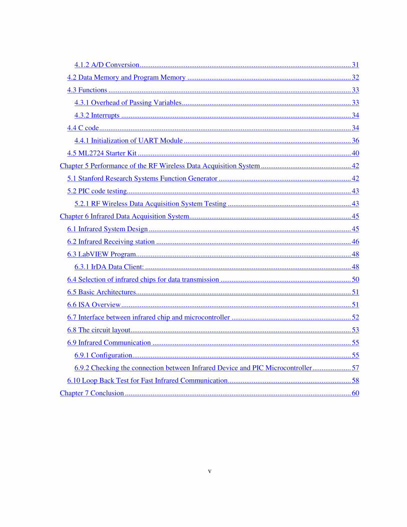
Bluetooth communicates on a frequency of 2.4 Gigahertz as shown in Figure 2-1, which has
been set aside by international agreement for the use of industrial, scientific and medical devices
(ISM). Many manufacturers produce radio devices taking advantage of this same radio-frequency
band. Baby monitors, garage-door openers and the newest generation of cordless phones all make use
of frequencies in the ISM band. Making sure that Bluetooth and these other devices don't interfere
with one another has been a crucial part of the design process.
8
Figure 2-1: International Radio Frequency Band Allocation
2.1.1 Avoiding Interference: Low Power
One of the ways Bluetooth devices avoid interfering with other systems is by sending out
very weak signals of 1 mill watt. By comparison, the most powerful cell phones can transmit a signal
of 3 watts. The low power limits the range of a Bluetooth device to about 10 meters, cutting the
chances of interference between computer system and portable telephone or television in home. Even
with the low power, the walls won't stop a Bluetooth signal, making the standard useful for
controlling several devices in different rooms.
With many different Bluetooth devices in room interference, devices operating at same
frequency can interfere with each other. Bluetooth devices tackle this problem using frequency
hopping and spread spectrum techniques. Since it is unlikely that several devices will be on the same
frequency at the same time Bluetooth devices uses a technique called frequency hopping spread-
spectrum. In this technique, Bluetooth device will use 79 individual, randomly chosen frequencies
within a designated range, changing from one to another on a regular basis. In the case of Bluetooth,
the transmitters change frequencies 1,600 times every second, meaning that more devices can make
full use of a limited slice of the radio spectrum. Since every Bluetooth transmitter uses spread-
spectrum transmitting automatically, it’s unlikely that two transmitters will be on the same frequency
at the same time. This same technique minimizes the risk that portable phones or printers will disrupt
Bluetooth devices, since any interference on a particular frequency will last only a tiny fraction of a
second.

9
Figure 2-2: Frequency Hopping and Piconets
2.1.2 Personal Area Networks
When Bluetooth-capable devices come within range of one another, each device discovers
another using “Service Discovery Protocol”. Bluetooth systems then create a personal-area network
(PAN), or piconet. Once a piconet is established as showing in Figure 2-3, the members randomly
hop frequencies in unison so they stay in touch with one another and avoid other piconets that may be
operating in the same room. Pico-networks reduce interference between multiple Bluetooth devices.
Following discussion explains how Bluetooth frequency hopping and personal-area network keep
systems away from becoming confused.

10
Figure 2-3: Piconet in House
Typical Bluetooth applications include connecting PC to printers, wireless headset to mobile
phone and cordless telephone to notebook. Each of these systems uses Bluetooth and each form their
own piconet. The PC has Bluetooth transmitter station working as base stand printer has its own.
Each unit is programmed with an address by manufacturing company that falls into a range of
addresses it has established for a particular type of device. When the base is first turned on, it sends
radio signals asking for a response from any units with an address in a particular range. Since the
printer has an address in the range, it responds, and a tiny network is formed. Similarly, wireless
headset forms piconet with mobile phone. Now, even if one of these devices should receive a signal
from another system, it will ignore it since it’s not from within the network. Once the networks are
established, the systems begin talking among themselves. Each piconet hops randomly through the
available frequencies, so all of the piconets are completely separated from one another.
Each piconet is made up of devices that know the address of transmitters it should listen to
and the address of receivers it should talk to. Since each network is changing the frequency of its
operation thousands of times a second, it’s unlikely that any two networks will be on the same
frequency at the same time. If the two networks are on same frequency at any instant, then the
network which is not supposed to hear will hear it as noise for that tiny fraction of a second. Usually,
Bluetooth soft ware is designed to correct such noise that appears on the network.

11
2.2 Frequency Hopping Technique
Spread spectrum technology can be implemented in several different ways, Bluetooth devices
commonly use frequency hopping. Frequency hopping technique is efficient utilization of free
2.4GHz ISM band available. The basic idea behind frequency hopping is simple instead of
transmitting on one frequency, a spread spectrum system switches rapidly from one frequency to the
next. The choice of the next frequency is random, so it is nearly impossible for someone to eavesdrop
or jam the signal. The Bluetooth device hops to the next frequency according pseudo-random number
generator. The challenge is to keep both the transmitter and receiver synchronized with accurate
clocks and pseudo-random number generators. In frequency hopping transmitter and receiver
continuously hop between frequencies and keep synchronized. Frequency hopping makes wireless
network secure and difficult for eaves dropping by other systems. Using a MicroLinear solution
frequency hopping can also be done.
The attractive feature of frequency hopping is effective utilization of limited frequency
spectrum. It is getting harder and harder to find clear channels on the crowded airwaves. Spread
spectrum technology gives engineers a way to fit Bluetooth devices into an existing spectrum without
jamming the devices already using it. Assume a PC is transmitting at 1 watt, but is hopping between
dozens or hundreds of channels very rapidly. Other devices don't see the phone because it is
transmitting for only a fraction of a second on any channel. Therefore, the average perceived power
on any given channel is extremely low, and other devices using that channel don't even notice it. The
phone creates the equivalent of a low-power noise pattern across all of the channels it uses. Other
devices deal with noise already, so the phone is essentially invisible to devices using specific
channels.

12
Figure 2-4: Frequencies hopping with respect to time
2.3 Interfacing to PC
Bluetooth SIG (Special Interest Group) has defined that USB, RS232 (serial cable), UART,
and PC Card are alternatives for a Bluetooth module to be connected with a PC (host). Bluetooth SIG
has specified the standardized interfaces for the USB, RS232, and UART.
2.4 Infrared Data Transfer (IrDA)
Infrared refers to light waves of a lower frequency than human eyes can receive and interpret.
Infrared is used in most television remote control systems, and with a standard called IrDA (Infrared
Data Association), it's used to connect some computers with peripheral devices.
Infrared devices communicate reliably and are available at low costs, but they have some
disadvantages. First, infrared is a "line of sight" technology. For example, infrared remote control
should be pointed at the television to control it. The second drawback is that infrared is almost always
a "one to one" technology. Data can be sent between a desktop computer and a laptop, but not
between a laptop computer and a PDA at the same time. These disadvantages are application specific.
For the application in hand, one to one technology is not an issue. Since infrared transmitters and
receivers have to be lined up with each other, interference between devices is uncommon. The one-to-
one nature of infrared communications is useful in that you can make sure a message goes only to the
intended recipient, even in a room full of infrared receivers.

13
Depending on the modulation scheme used, infrared communications can be done in various
types such as Fast Infrared (FIR), Medium Infrared (MIR), Serial Infrared (SIR), Consumer IR (CIR)
and Sharp ASK IR. The IrDA (Infrared Data Association) is aimed to allow its standards to support a
wide class of computing devices and peripherals that might be used by mobile professionals. These
devices would range from very sophisticated, high-power notebook or laptop personal computers,
through palmtop computers and personal digital assistants, to simple single-function devices like
electronic business cards or phone dialers. It was also envisaged that IrDA would enable new classes
of devices such as information access points. To target such a broad range of devices, a set of general
requirements was placed on any prospective standard.
These requirements included:
a) Low cost
b) Industry standard
c) Compact, lightweight, low-power
d) Intuitive and easy to use
e) Non-Interfering.
Figure 2-5: Infrared Network
IrDA has specified the physical and protocol layers necessary for any two devices that
conform to the IrDA standards to detect each other and exchange data. The initial IrDA 1.0
specification detailed a serial, half-duplex, asynchronous system with transfer rates of 2400 bits/s to
115,200 bits/s at a range of up to one meter with a viewing half-angle of between 15 and 30 degrees

14
(Figure 2-6). IrDA has extended the physical layer specification to allow data communications at
transfer rates up to 4 Mbits/s. Most recently, it has announced physical layer specification for VFIR
(very Fast Infrared -16 Mbits/sec). FIR communications is selected for this application because of
high data rates it offers.
Figure 2-6: Viewing Angle specified in IrDA specification
2.4.1 The IrDA Architecture
In the basic IrDA model, there are two devices. One is the primary and the other is the
secondary. The primary device is responsible for selecting a device within its visual space,
establishing a connection, and maintaining the virtual wire or link. The secondary responds when
spoken to. At the beginning of a typical IrDA operation, the primary initiates a process known as
“discovery”, in which it explores its visible space for devices. From those devices that respond the
primary selects a device and attempts to connect to it. During connection establishment, the two
devices negotiate to understand each other’s capabilities. In this way a connection can be optimized
despite the unpredictable differences between two disparate devices. Once they have negotiated, they
will jump to their highest common transmission speed, and attempt to communicate in ways that
optimize the throughput and reliability of their connection. Having established a connection, the
devices may now search the services of the other devices. If the other device supports a desired
service, a connection can be made to the service. At this point, applications on either side of the
connection can transfer data. Obviously there are considerably more details than that have been
presented here, and the IrDA specifications are the definitive source for that information.

15
Figure 2-7: IrDA Protocol Stack
The IrDA protocols are organized in a traditional layered or stacked architecture (Figure 2-7). IrPHY
specifies optical characteristics, encoding of data, and framing for various speeds.
The IrPHY specification was quickly followed with the publication of the Infrared Link
Access Protocol (IrLAP). IrLAP specifies an HDLC-based protocol for controlling access to the
infrared medium and providing the basic link-level connection between a pair of devices.
During the development of IrPHY and IrLAP, it was realized that some additional functionality was
required in addition to the ability to provide a single connection between a pair of devices. The
Infrared Link Management (IrLMP) layer was conceived. This layer has two primary functions.
First, it provides the mechanism by which multiple entities within any pair of IrDA devices
can simultaneously and independently use the single IrLAP connection between those devices. IrLMP
multiplexes services and applications on the LAP connection. This function is called the link
management multiplexer (LM-MUX). Second, it provides a way for entities using the IrDA services
to discover what services are offered by a peer device and to register available services within the
local device. This link management information access service (LM-IAS) considerably benefits the
ease of use of portable devices, allowing pairs of devices to interrogate each other to discover
information about the applications within each device. These three standards—IrPHY, IrLAP, and
IrLMP—form the core of the IrDA architecture, and all are required for a device to be IrDA-
compliant. The current complete IrDA architecture is shown in Figure 2-7.

16
In addition to the base standards, IrDA has specified a protocol called Tiny TP. This protocol
is an extremely lightweight transport protocol designed to provide application-level flow control as
well as segmentation and reassembly of application data units. This protocol has proved to be useful
and is now implemented by most applications that support the IrDA architecture. To complement the
functionality of the main components of the IrDA architecture, several application-level protocols
have been and are in the process of being developed. These protocols are aimed at providing
convenient and uniform interfaces to the functionality of the IrDA protocols for both old and new
applications. The receiver and transmitter section for infrared communications should use the same
IrDA architecture and protocol. For example, if a laptop wants to communicate with an infrared port
on printer, application running on the laptop should use same protocol stack and IrDA architecture
used on printer.
2.4.2 The IrDA Physical Layer
IrDA data communications operate in a half-duplex mode. The reason is quite simple. While
transmitting, a device’s receiver is blinded by the light of its own transmitter. Because of this, full
duplex communication is not feasible. The two devices that communicate simulate full duplex
communication by quickly turning the link around. The primary device controls the timing of the link,
but both sides are bound to certain hard constraints and are encouraged to turn the link around as fast
as possible.
2.4.2.1 Framer
The Physical layer includes the optical transceiver, and deals with shaping and other
characteristics of infrared signals including the encoding of data bits, and some framing data such as
begin and end of frame flags (BOFs and EOFs) and cyclic redundancy checks (CRCs). This layer
must be at least partially implemented in hardware, but in some cases is handled entirely by hardware.
In order to isolate the remainder of the stack from the ever-changing hardware layer, a software layer
called the framer is created. Its primary responsibility is to accept incoming frames from the hardware
and present them to the Link Access Protocol layer (IrLAP). This includes accepting outgoing frames
and doing whatever is necessary to send them. In addition, the framer is responsible for changing
hardware speeds at the bidding of the IrLAP layer; using whatever magic incantations the hardware
designer invented for that purpose (these signals have not yet been standardized). CRC (error
17
checking on data received) can be implemented in hardware or software. BOF synchronize
transmitter and receiver.
2.4.2.2 Driver
The driver portion refers to the software that acts as a device driver for the system’s
transceiver controller. This driver initializes the infrared hardware; changes transmission speeds,
delivers data to the transceiver, and receives data from the transceiver. Drivers implement some of the
protocols such as IrCOMM, IrOBEX. The choice of driver depends on the application of interest.
The IrDA physical layer is split into three distinct data rate ranges: 2400 to 115,200 bits/s,
1.152 Mbits/s, and 4 Mbits/s. Initial protocol negotiation takes place at 9600 bits/s, making this data
rate compulsory. All other rates are optional and can be added if a device requires a higher data rate.
The links are designed to be used in a line-of-sight, point-and-shoot manner and hence have a modest
minimum coverage of one meter, with a ±15° viewing angle. The details about 2400 to 115200 bit/s
and 1.152 Mbits/sec are described elsewhere [3]. This section describes about 4 Mbits/s modulation
scheme and framing.
2.4.3 The 4-Mbit/s Link
The 4-Mbit/s link architecture is shown in Figure 2-8. In 4-Mbits/s link, packet framing and
CRC generation and checking are performed in hardware to relieve the burden on the host processor,
while higher-level protocols are implemented in software on the host processor. The link uses a 4
PPM encoding scheme (described below) and robust packet structure. A phase-locked is used as
means of recovering the sampling clock from the received signal. PC chipsets including the 4-Mbit/s
hardware are already available from leading semiconductor manufacturers. FDC37C672 from SMSC
is used to perform Fast Infrared (FIR) communications. Packet Framing and CRC generation are done
inside this chip and this relieves the burden on the software.

18
Figure 2-8: 4-Mbits/sec Link Architecture
2.4.3.1 Encoding and Packet Format
Pulse position modulation (PPM) was chosen as the line code for the 4-Mbit/s link. Data is
transmitted within a PPM signal by varying the position of a pulse (referred to here as a chip) within a
symbol (referred to here as a cell). The PPM modulation for the 4-Mbit/s link allows one chip to be
set in one of four possible positions; thus it is known as 4PPM. Since a chip can be set in one of four
possible positions, four different messages can be sent within one cell, allowing two bits of data to be
encoded per cell. Figure 2-9: 4PPM Message Encoding shows the four possible messages that can be
transmitted by 4PPM.
Figure 2-9: 4PPM Message Encoding

19
Pulse position modulation has many properties that make it attractive for use on the free-
space optical channel. One of the main properties is the sparseness of the code. Sparse code allows
high peak powers to be employed for set chips while maintaining a reasonable average power. The
eye-safety rules stipulate a maximum average optical power, and LED’s tend to be average-power-
limited at moderate duty cycles.
Pulse position modulation also contains significant and regular timing content, which
facilitates synchronous clock recovery using a phase-locked loop. It is a modulation format that has
very little dc content and can be high-pass filtered at 100 kHz, avoiding interference generated by
fluorescent lighting without adversely affecting the receiver’s eye diagram. A particularly interesting
feature of PPM—one that had important ramifications in the choice of end delimiters—is its ability to
detect line code errors.
Higher orders of PPM give lower duty cycles and theoretically greater signal-to-noise ratio
gains on the infrared medium. Figure 2-10 illustrates the interesting relationship between signal-to-
noise ratio gain achievable with various orders of PPM and the required pulse width. It is interesting
to note that the optimum order of PPM from a bandwidth efficiency perspective would be 3PPM.
This result might be of theoretical interest, but is fairly useless in a practical system. Since the fastest
bright LEDs have a rise time of around 40 ns, and the rise time of an LED is proportional to the pulse
width, the use of high-order PPMs at 4 Mbits/s becomes impractical. The decision to adopt the order
four for the PPM was motivated by knowledge of the range of duty cycles over which LEDs are peak-
power-limited, the rise and fall time of available LEDs, and the frequent timing content provided at
order four.
Figure 2-10: Signal –to-Noise Ratio gain and pulse width trade-off

20
2.4.3.2 Packet Format: The 4-Mbit/s physical layer packet has distinct features that perform a
useful and well-defined role (see Figure 2-11). A preamble allows dc balance to be attained, and more
important, permits the phase-locked loop to achieve chip-level synchronization. The length of the
preamble was considered carefully such that the preceding two goals could be achieved without a
significant impact on efficiency. The start and stop delimiters provide cell and frame synchronization
and were chosen so as not to compromise overall packet robustness or adversely affect the receiver
eye diagram. To distinguish the preamble and the end delimiters from the frame body, these fields
contain code violations. The body of the packet is 4PPM-coded and has a 32-bit cyclic redundancy
check (CRC) field appended to it. The choice of a 32-bit CRC provides a guaranteed level of
robustness to undetected data errors over the range of error rates expected on a free space infrared
channel. The CRC is performed on the data bits rather than on the PPM-encoded chips. Packet
framing and modulation are done inside Infrared Communication Controller (FDC37C672).
Figure 2-11: 4-Mbits/sec packet format
For technical reasons, the transceiver and controller are separate physical modules and are
often manufactured by different suppliers. In principle, a mixed-signal module containing transceiver
and controller functions would be desirable but is considered a major technical design challenge
because of potential interference between the circuits carrying the small photon-induced currents and
those carrying digital signals. Even so, system integrators have encountered problems that are related
to the interface between transceiver and controller when operating in the 4 Mb/s IrDA mode (called
Fast Infrared or FIR) based on four-slot pulse position modulation (4-PPM).
2.4.4 Interfacing to PC
Typically Infrared devices are connected to the PC through the USB and serial ports. There
are some vendors who develop ISA and boards with Infrared, Serial and Parallel Port Connectivity on
these boards. Since the chip on these boards can provide Infrared, Serial and Parallel Port
functionality; these chips are called as Super I/O (Input/Output) chips.
21
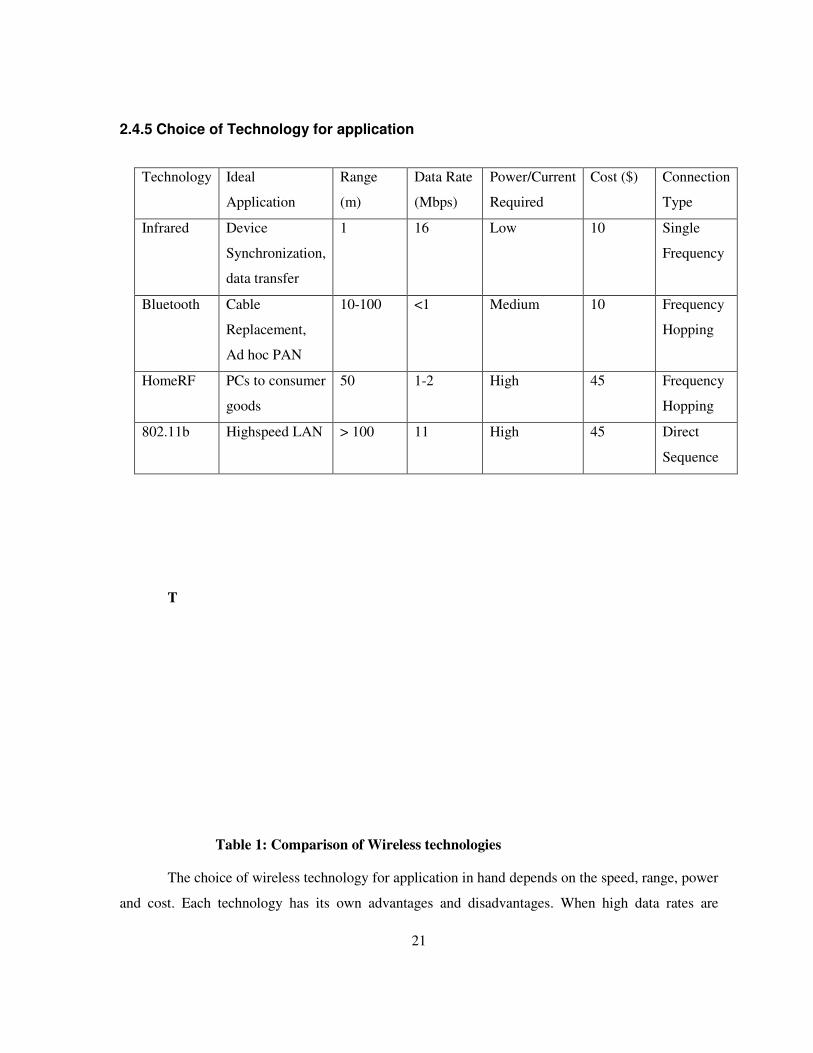
2.4.5 Choice of Technology for application
T
Table 1: Comparison of Wireless technologies
The choice of wireless technology for application in hand depends on the speed, range, power
and cost. Each technology has its own advantages and disadvantages. When high data rates are
Technology Ideal
Application
Range
(m)
Data Rate
(Mbps)
Power/Current
Required
Cost ($) Connection
Type
Infrared Device
Synchronization,
data transfer
1 16 Low 10 Single
Frequency
Bluetooth Cable
Replacement,
Ad hoc PAN
10-100 <1 Medium 10 Frequency
Hopping
HomeRF PCs to consumer
goods
50 1-2 High 45 Frequency
Hopping
802.11b Highspeed LAN > 100 11 High 45 Direct
Sequence

22
required with low power consumption within very short range infrared becomes obvious choice. If
security and range are important with moderate data rates, Bluetooth is attractive. There are also other
technologies such as Wi-Fi (802.11b) and HomeRF which can provide wireless connectivity. The
table below summarizes range, data rate, power, cost and Modulation scheme for different wireless
applications.
Chapter 3
Embedded RF Wireless Data Acquisition System
3.1 Conceptual Model of the Embedded Wireless Transmission System:
The main goal of the project is to transmit data from a sensor to Desktop in wireless
format. Figure 3-1 shows basic circuit diagram to transmit data from a sensor to a Desktop PC
through the wireless medium. The blue box represents the sensor which measures physical activity
and converts it to analog electrical signal. The microcontroller (red box) acquires analog data from a
sensor and converts it into digital format. Digital data is transferred to transmitting station (green box)
which modulates digital data to wireless signal and transmits it. The receiving station which is in
yellow receives the wireless data, demodulates the wireless data into digital data and transfers it to
Desktop PC.

23
Figure 3-1: Embedded Wireless Data Acquisition System Model
Since the main objective of this thesis is to demonstrate a wireless transmission system,
signal conditioning (anti-aliasing filters and amplification) needed to acquire data from a sensor is not
discussed in detail here. Description of signal conditioning and anti-aliasing can be found in [17].
Radio Frequency wireless transmission is the main topic of this chapter. This chapter
discusses wireless transmission of data from sensor to Desktop PC through Radio Frequency (RF)
Medium. In Chapter 4, components of RF wireless transmission system will be described in detail. In
this chapter, the overall system will be explained in more general terms.
Figure 3-2: RF Data Acquisition system design
3.2 RF Data Acquisition System
The data acquisition system developed for the RF system consists of a microcontroller
PIC18F452 and ML2724 Transceiver. The PICDEM2 board from Microchip is used to download the
code onto the PIC microcontroller. After the final code is debugged, the PCB board is designed and
the PIC microcontroller is soldered onto the PCB board. The ML2724 starter kit from Micro Linear is
used to convert digital data from the PIC microcontroller into RF format. Figure 3-3 below shows the
embedded RF wireless system with components and interface.

24
Figure 3-3: RF Wireless Data Acquisition System with components and interfaces
3.3 PIC 18F452
PIC is a member of Microchip's popular PICMicro (TM) line of microcontrollers. The
PIC18F452 [5] is selected as microcontroller to develop the embedded RF Wireless system because
of the built-in USART support (RS 232) and A/D converter. Built-in USART and A/D converter
modules execute in parallel with CPU, thus saving lot of CPU time. Also, the PIC18F series has a
large number of I/O ports which come handy for debugging and other applications. Shown in Figure
2.4 is the PICDEM-2 board from Microchip. PIC-DEM2 is PIC development board from Microchip
to debug and program PIC18F452. PIC18F452 MCU can also be seen in Figure 3-4. A USB
programming connector (ICD2 Header) is used to download C code onto the PIC MCU and a UART
connector is used to access its UART pins. 40 MHz clock oscillator is used to run internal instruction
cycle of PIC microcontroller.
Figure 3-4: PICDEM-2 Board with PIC18F452
The Microchip In-Circuit Debugger (ICD) is used for programming and debugging the PIC
MCU on PIC Development Board (PICDEM-2). The ICD debugger is connected between a USB port
on the PC and ICD Header on the PICDEM-2 board as shown in Figure 3-5.
PIC18F452

25
Figure 3-5: Connection between ICD2 debugger, PICDEM-2 and PC
The ICD can also be used as a programmer, which eliminates the need for an external
programmer. The Microchip Integrated Development Environment, MPLAB-IDE is used to develop
PIC MCU code. The MPLAB-IDE software provides user-friendly debugging environment to debug
PIC18F452 on PICDEM-2 board. The MCC-18 C compiler from Microchip is added to MPLAB-IDE
to develop C code. The MCC-18 C compiler converts C code into assembly code. Assembly code
generated by C compiler is converted into op-codes and downloaded into the PIC MCU using ICD
debugger. Another advantage of the ICD debugger is that it can set breakpoints in C code so that the
microcontroller registers can be accessed in real-time while the code is executing. The RF
transmission component ML 2724 Starter Kit is discussed in the next section.
3.4 ML 2724 Starter Kit
The ML 2724 starter kit [6] from Micro Linear is shown in Figure 3-6. This is rhe
development board from Micro Linear on which the ML2724 Transceiver is soldered. The ML2724
Transceiver on this starter kit handles the wireless communication. This transceiver is the heart of the
board. We will refer to this board as the RF board.
Figure 3-6: ML 2724 Starter Kit from Micro Linear
ML22724 Transceiver
Firmware IC

26
3.5 Analog Section of the Data Acquisition System
This section discusses the A/D converter of the PIC18F452 microcontroller [5]. The
microcontroller PIC 18F452 from microchip is used to convert analog data from the sensor to digital
format. The PIC MCU converts signal on its ADC pins into 10-bit binary format. An ADC will have
upper and lower reference voltages. On 10-bit A/D converter, the voltage spacing between upper and
lower limit into 102 discrete steps. Resolution of A/D converter on the PIC microcontroller is (upper
limit – lower limit)/102 . This would be smallest voltage level detected by the PIC microcontroller
with 0 and 5Volts as reference. The default ADC references if not configured by the PIC are 1) Upper
limit is the Supply Voltage 2) Lower limit is GND. For this application, the upper limit is 5V and the
lower limit is GND or 0V. Resolution of A/D converter = (5-0)/1024=0.00488V=4.88mV.
3.6 Receive and Display components
The receiving station receives the data transmitted wirelessly from the transmitting station
and transfers it to the PC. The ML2724 evaluation board made by Micro Linear for the purposes of
evaluating their ML2724 transceiver is used as the RF wireless reception station.
Figure 3-7: The ML2724 evaluation board is used to wirelessly communicate with the PIC. a. A
close-up of the Evaluation board. b. The evaluation board is connected to the PC through a
serial cable. The LabVIEW interface code is seen on the computer display.
Once a wireless connection is established with a proper configuration, data received by the
evaluation board from the transmitting station is sent through a serial cable to the computer. The
LabVIEW graphical user interface code (GUI) is used to display data collected from the sensor on the

27
computer’s screen. Since LabVIEW makes it easy to collect data and display data on graph,
LabVIEW is used for developing the final user interface.
Figure 3-8: LabVIEW front panel showing received data
The LabVIEW front panel on receiving side is shown in Figure 3-8. The waveform graph is
used to display a single set of samples received from the computers RS232 buffer. As soon as a
complete message packet is received without errors, it is displayed on the waveform graph. The
section “Serial Port settings” on the front panel allows the user to change the serial port number
(COM1, COM2), baud rate, data bits size and parity bits. The port number is used to change the serial
port which accesses received data. Baud rate is used to select the serial transmission baud rate. All the
serial port settings are set by default to the parameters at which the ML 2724 board works so that user
need not worry about serial port settings.
The “Received Data” indicator on the front panel shows the recent complete message packet
received through the serial port in string format. “Bytes in the buffer” indicate the number of samples
received by the port and the “string read” shows the received string of data in ASCII format. “Packet
Information” on the front panel displays the information of the packet received. RF Transmitter sends

28
data in form of messages/packets. Each packet has a packet number, address of the receiving station,
Data and an End-of-Packet character inside packet. End-of-Packet character is also called as
“termination character”. Figure 3-9 shows typical packet type sent by the transmitter. For example, a
packet/message looks like 01: FC: KJLFGJF\n. 01 is the packet number, FC is the receiver address,
KJLFGJF is data in the packet and \n is the termination character.
Figure 3-9: Message Packet encoded ML2724 Starter Kit
As soon as a data packet is obtained inside LabVIEW, header (packet number and address
portion) is detached from the data packet. Important header information such as Packet number is
displayed on the front panel. Data or information starts from end of data packet number portion and
ends with termination character. In the LabVIEW program the number of information bytes inside a
Data Packet are counted and presented on the front panel.
The program setting section has a control “Milliseconds to wait”. The “Milliseconds to wait”
control allows the user to adjust the amount of time between each successive read of the computer
serial port buffer. A larger “milliseconds to wait” value means that more time is allowed for samples
to enter the buffer before a read so that on the next read cycle more samples will be received and
displayed on the waveform graph. Alternatively, a smaller “milliseconds to wait” value will result in
fewer samples displayed in the waveform graph display. The write section on the front panel is used
to write data through a serial port to the ML2724 Starter Kit. ML2724 Starter Kit Transceiver is
enabled to receive data by writing AT+XCEN=1\n through serial port.
LabVIEW enables easy access to a computer’s serial port through the use of built-in Virtual
Instruments (VIs). VISA Configure Serial Port.vi initiates connection to a serial port. Baud Rate,
Parity are set using VISA Configure Serial Port.vi. VISA Write.vi is used to write data to a serial
port. VISA bytes from serial port.vi determine the number of bytes in the serial port buffer and VISA
Read.vi data can be read from a serial port. VISA Close.vi closes connection to a serial port. If the
serial port connection is not closed, memory leakage occurs.

29
Remove Header.vi and Packet Decoder.vi separates data from the RF packet received through
the serial port. Queues are used to buffer data received from the serial port until complete data packet
is received into LabVIEW. The LabVIEW program’s front panel is shown in Figure 3-8. The
waveform graph is used to display the samples received from the computers RS-232 buffer. Queues
are used in LabVIEW to synchronize data reception from the serial port and display on the front
panel. As soon as a complete packet is received from the serial port, it is displayed on the waveform
graph. Number of data bytes inside RF data packet is fixed as 64 bytes in the C code inside PIC
microcontroller.

30
Chapter 4
Components of RF Wireless Data Acquisition System
This chapter takes a closer look at the Microchip PIC18F452 and the Micro Linear ML2724
Transceiver module [7], shown in green in Figure 2-3. The PIC18F452 MCU and its C language
program are to be discussed next. Finally, the ML2724 module and its wireless protocol are
discussed.
4.1 PIC Microcontroller and C Program
The PIC18F452 is a general purpose MCU from Microchip. It has several convenient built-in
modules such as A/D, UART, SPI, PSP etc., which reduce development time. In particular, an on-
chip Analog to Digital Converter (ADC) eliminates the need to design separate ADC circuitry. Also,
an on-chip Universal Asynchronous Receive Transmit (UART) module makes asynchronous
communication with the ML2724 Transceiver Module relatively simple. ADC and UART modules
operate in parallel with the microcontroller’s CPU. Operation of A/D and UART modules in parallel
with CPU saves CPU instruction cycles. In other words, once ADC and UART are configured
properly, they operate almost independently with the CPU inside PIC Microcontroller.
4.1.1 UART Communication
The PIC MCU and ML2724 Starter Kit communicate with one another using a UART interface.
The UART communication is a digital data packet communication scheme. The data packet consists
of eight binary data bits of information. A start bit is sent as a prefix to the eight bits of data and
either one or two stop bits may be appended to the data packet. A parity bit can also be appended for
error checking.
The PIC and the Starter Kit communicate using a one stop bit, 8 data bits, single stop bit for a
total packet length of ten bits. No parity bits are used for UART communication between the PIC and
the ML2724 Starter Kit. PC and ML2724 Starter Kit communicate through serial (RS232) interface.
RS232 and UART communication are exactly the same except that the voltage levels used to
represent binary ones and zeros are different. In typical UART interface binary one and zero are 5
and 0Volts respectively. RS-232 binary one and zero levels are represented by +10V and -10V. A line

31
driver is an electronic device that may be used to switch between UART and RS232. These line
drivers have an internal charge pump to create +10 volts and -10 volts. Using the UART module is a
simple matter of configuring the UART module and loading the appropriate registers with the data to
be exchanged. A variety of baud rates may be used, but the PIC’s UART baud rate was set as close
as possible to the baud rate of the ML2724 Starter Kit module’s UART baud rate of 57.6 kbaud. The
PIC’s UART baud rate was configured for 57.6 kbaud, which result in a baud rate error of when
matched to 57.6 kbaud.
4.1.2 A/D Conversion
The PIC’s ADC module can handle up to 8 separate channels but can only acquire sample
from single channel at an instant i.e., the PIC’s ADC can be configured to perform sequential
sampling. A 10-bit Successive Approximation Register (SAR) is used to do the conversion. The
PIC18F452 has its (General Purpose Input / Output) PORTA and PORTE multiplexed with Analog
Inputs of its A/D converter. To acquire data from Analog Inputs of PIC18F452, ADCON0 and
ADCON1 register should be configured. Since PIC 18F452 has 10-bit A/D converter, the result of the
PIC microcontroller A/D conversion is stored in two registers in PIC microcontroller. The lower 8
bits out of 10 bits are stored in ADRESL (A/D Register Low) and upper two bits are stored in
ADRESH (A/D Register High). The sequence below explains how to configure the PIC
microcontroller to acquire data from single channel continuously. PIC A/D Conversion steps:
1. Configure the A/D module:
• Configure analog pins, voltage reference and digital I/O (ADCON1)
• Select A/D input channel (ADCON0)
• Select A/D conversion clock (ADCON0)
• Turn on A/D module (ADCON0)
2. Wait the required acquisition time.
3. Start conversion:
• Set GO/DONE bit (ADCON0)
4. Wait for A/D conversion to complete, by either:
• Polling for the GO/DONE bit to be cleared (interrupts disabled)
5. Read A/D Result registers (ADRESH/ADRESL)

32
6. For next conversion, go to step 1 or step 2 as required. The A/D conversion time per bit is
defined as TAD.
A minimum wait of 2 TAD is required before the next acquisition starts. The delay between two A/D
conversions dictate sampling rate of the PIC MCU. If A/D converter collects samples at a rate greater
than the data it transfers through UART module, there will be data transmission loss. A/D converter’s
sampling rate for this application is dictated by UART transfer rate for this application. In subsequent
paragraphs, we will see that UART transfer rate for this wireless transmission is 57600bps (7200
bytes/sec). Since each A/D conversion generates 10 bits or 2 bytes of data for transmission, maximum
sampling rate of the A/D converter for this application cannot exceed 7200/2 = 3600 Hz. But later in
the chapter it will discussed that maximum sampling rate achieved in practice is 900Hz (less than the
estimated 3600Hz) due to limitation of firmware on the ML2724 board.
Before discussing the C code written for the PIC18F452, some basic Microcontroller
concepts that may be helpful for understanding the C code will be introduced. The concepts that will
be introduced, which were all used in the development of the code, are the hardware stack, interrupts,
and pointers.
4.2 Data Memory and Program Memory
The two different kinds of memory used on the PIC18F452 are data memory (RAM), and
program memory (ROM) [8]. Data memory (RAM) is divided into two different types of eight bit
registers: special function and general purpose. General Purpose Registers (GPRs) may be used to
store variables, while Special Function Registers (SFRs) are used to configure and control the MCU.
A variable defined in C is address of specific memory location inside RAM. All the constants are
stored inside ROM. In C, all variables must be declared before they are used. One of the biggest
advantages of C code is that it takes care of low-level details such as switching banks inside the PIC.
To save memory addressing space, Special Function registers are stored in banks/pages inside the
PIC18F452. This leaves more addressing space for General Purpose registers on the microcontroller’s
RAM. To access different registers banks are switched by writing bank number in Bank Select
Register (BSR).

33
Operations that tell the MCU what to do are called Operational Codes (Op-Codes) and they
are stored in program memory [8]. In the PIC18F452, there is nearly 2 Mb of addressable program
memory, which is executed sequentially from the top down. Only 32 Kbytes of this 2Mb is available
to store the program developed by the user. For more information on the 77 available Op-Codes
available for the PIC18F452, the interested reader should download the data sheet from [8]. When C
code is compiled it is converted into assembly code. This assembly code is a sequence of Op-Codes
Code to make microcontroller perform its operations.
A section is a portion of an application located at a specific address of memory. Sections can
contain code or data. A section can be located in either program or data memory. There are two types
of sections for each type of memory.
• Program memory
- Code – contains executable instructions
- romdata – contains variables and constants
• Data memory
- udata – contains statically allocated un-initialized user variables
- idata – contains statically allocated initialized user variables
4.3 Functions
Functions are defined for lateruse in code development. Properly defined functions can save
code space and significant development time . A function’s argument is a value that is passed to the
function when called. C allows zero or more arguments to be passed to a function. When a function is
defined, formal parameters are declared between the parentheses that follow the function name.
4.3.1 Overhead of Passing Variables
MPLAB-C18 uses a software stack for passing variables into functions and for returning
values from functions. This makes the compiler support complex functions and allows recursive
functions, but there is some overhead in managing the software stack. When compiling, the compiler
will examine the function and only include the appropriate level of stack support code. The STACK is
a series of registers that is used to save the value of the program counter so these locations of program
memory may be returned to. The number of parameters which can be passed into a specific function
34
depends on the depth of stack inside microcontroller. The stack depth also dictates number of external
functions that can be called inside a function call.
4.3.2 Interrupts
Interrupts are used to execute PIC code at full speed until some external or internal event
triggers the interrupt. Interrupts allow CPU to make efficient utilization of peripheral resources such
as the ADC or the UART. When an interrupt is triggered, the STACK is loaded with the current
program counter value, and the program disables interrupts and vectors to the location in ROM that is
dedicated to servicing interrupts. The PIC18F452 services a maximum of two interrupts at a time by
prioritizing them. In the case of the PIC18F452, this area of program memory is located at address
0x008. When the interrupt has been serviced, a “retfie” command (in assembly language) may be
used to return to the location in theROM. The “retfie” command also automatically re-enables the
interrupts. If the “retfie” command is not used the STACK is not unloaded and the stack must be
manually unloaded using the “pop” Op-Code to remove the top layer of the stack and avoid overflow.
Interrupts are declared in C code using pragma statements. For example,
#pragma code high_vector=0x08
This statement starts the interrupt at location 0x08 and the memory location of code for the interrupt
service routine is stored at this location.
4.4 C code
C code written for the PIC18F452 uses all of the concepts discussed thus far in section 3.2.
To reduce development time, programming is done in C instead of assembly level programming. C
code also eliminates the need to take care of switching banks inside microcontroller for register
access. In Appendix B, the C program for radio frequency transmission is included. This code was
developed in the Microchip Integrated Development Environment (IDE) version 6.10, which may be
downloaded from Microchip’s Website for free [9]. C code is developed using Microchip MCC18 C
compiler [10]. Application Maestro from Microchip is used to develop C code needed for UART
communications. A flow chart describing the sequence of code will be discussed in next paragraph.

35
Start
Initialize UART
(baud rate,
interrupts)
Set up ADC
(Channel 0)
Configure
ML2724 for
Transmisison
Delay
Acquire sample
Check buffer
space and add
to buffer
Figure 4-1: Flow chart explaining code on PIC18F452
Shown in Figure 4-1 is a simplified flow diagram of the C code. The oval labeled “start” in
Figure 4-1 indicates where the program begins. In C code is the main ( ) statement. The first thing that
the program does is initialize the MCU’s UART and ADC, setup interrupts, and send the proper
commands to the ML2724 Starter Kit module to setup a wireless connection. More information on
these commands will be given in section 4.5.

36
4.4.1 Initialization of the UART Module
The UART is initialized to transmit data from the PIC microcontroller to the ML2724
board.
First –In First-Out (FIFO) buffer is created inside microcontroller to increase buffer size of the UART
module. The UART module transmits data through interrupts. The UART module triggers an
interrupt as soon as it finishes transmitting a byte available in the Transmit Shift Register. The
Transmit Shift register obtains its data from the read/write transmit buffer register TXREG (Transmit
Register). The TXREG register is loaded with data from FIFO buffer when interrupt occurs. The TSR
register is not loaded until the last bit has been transmitted from the previous load. As soon as the last
bit is transmitted, the TSR is loaded with new data from the TXREG (if available). Once the TXREG
register transfers the data to the TSR register (occurs in one TCYCLE), the TXREG is empty and the
interrupt bit TXIF (Transmit Interrupt Flag) inside the Peripheral Interrupt Request Register 1(PIR1)
is set. As soon as this bit is set to one an interrupt occurs.
UARTIntInit ( ):
This function initializes USART module inside the PIC microcontroller. Initialization of the UART
module involves a) enabling the UART module/ Serial Port b) selecting the baud rate using register
SPBRG c) setting up the UART module to perform both transmission and reception d) configuring
transmission and reception interrupts. This function clears the user defined (FIFO) buffers and
initializes error and status flags to appropriate values.
Void UARTIntISR (void):
This is the Interrupt Service Routine function (ISR) for serial transmit and receive interrupt. The PIC
microcontroller enters into the Interrupt routine as soon as the UART module triggers the interrupt.
The UART module triggering condition is discussed in UARTIntinit ( ). This needs to be called from
the interrupt service routine in user’s main application at proper interrupt vector (low or high priority
vector).
This function transmits the byte in the buffer pointed by index vUARTIntTxBufRdPtr, updates the
read index to buffer and decrements vUARTIntTxBufDataCnt (number of bytes in transmit buffer not
yet transmitted).

37
Figure 4-2: Software buffer inside PIC microcontroller and its pointers
The above functions describe the code for handling serial transmission of data through UART
interface to the ML2724 starter kit. This section describes the code initialize A/D converter
module inside the PIC microcontroller.
// configure A/D converter
OpenADC (ADC_FOSC_8 & ADC_RIGHT_JUST & ADC_8ANA_0REF, ADC_CH0&
ADC_INT_OFF);
OpenADC ( ):
This function sets up the A/D module inside the PIC microcontroller to start analog to digital
conversion. This function can be used to choose to select analog channels on the PIC, select
reference voltage for analog channel. This function also enables interrupts for A/D conversion.
For the current application analog channel 0 is selected, reference voltage for this channel are
selected as GND and VCC. Interrupts for A/D conversion are not enabled. This is discussed in
detail in main program section.
ConvertADC ( ) starts A/D conversion
BusyADC ( ) informs the status of A/D conversion.

38
Main Program main( ):
The main( ) function is the main section of the code where the main sequence of application is done.
UARTIntInit ();
This statement initializes UART module to transmit data at 57600 bps.
OpenADC (ADC_FOSC_8 & ADC_RIGHT_JUST & ADC_8ANA_0REF,
ADC_CH0 & ADC_INT_OFF);
This statement initializes A/D converter with
a) ADC_FOSC_8 : Frequency of A/D converter is 1/8 times of 40 MHz = 5MHz This is not the A/D conversion rate. This is the clock A/D converter module uses to time A/D
conversion.
b) ADC_RIGHT_JUST: Result is in Least Significant bits.
c) ADC_8ANA_0REF: Upper Voltage Reference for analog channels is VDD (Power Supply), Lower Voltage reference for analog channels is VSS (GND).
d) ADC_CH0: Only channel 0 is selected for data acquisition.
e) ADC_INT_OFF: Interrupt generated A/D module is disabled.
Delay1KTCYx (22):
This statement introduces a delay of 22,000 (22K) instruction cycles between consecutive A/D
conversions. A 40MHz clock is used to run the PIC microcontroller for this application. In PIC
microcontroller, each instruction is pipelined into 4 cycles. Effectively, each instruction cycle takes
1/10= 0.1 microseconds. Delay introduced by 22000 instruction cycles is 22000*0.1 microseconds =
2.2 milliseconds. Therefore, the effective A/D sampling rate = 1/2.2 KHz = 454.5 Hz

39
By changing the integer inside the delay function, delay between A/D conversions can be
changed and thus sampling rate can be changed. The rest of the code is well commented and
describes transmission of digital data collected by the A/D converter through the UART
module. Code is included in appendix section.\r, \0 are termination characters for the ML2724
packet. If A/D conversion result is equal to \r,\0 (ASCII) then transmission packet from the
ML2724 transmitter doesn’t reach receiving side. To eliminate this problem, A/D converter is
incremented by 1 and transmitted. This increment is decremented on the final receiving station.
RF transmission from the microcontroller to the PC is discussed in subsequent paragraphs. Data
acquired using the PIC microcontroller is transferred to the ML2724 board through UART
Interface (Serial Bus). The PIC18F452 microcontroller has built-in USART module. UART
registers inside USART module of PIC18F452 are configured to transmit data as described in
UART initialization section above.
Once UART is configured, data is moved from ADRES registers to UART register through
FIFO buffer. Writing data into UART register before data is transmitted to the RF Board may
result in overwriting of data. To eliminate this problem, buffer is used. Overwriting of data also
results in loss of data as it is not transmitted to the RF Board. Overwriting occurs because
UART module doesn’t have enough buffer size to transmit A/D data. To solve this problem, a
software circular buffer is implemented inside the PIC microcontroller. Buffer size can be
reconfigured in the code depending on application requirements.
To enable proper data transmission between UART devices
1) Both UART Devices should be configured to operate at same speed
2) UART devices should follow same packet format i.e., same number of data, stop and
parity bits.
Two UART devices will not communicate with each other until the above requirements are
met. The UART in the PIC should be configured to work with the same baud rate and packet
format as the RF board. Firmware on the RF board communicates at baud rate of 57600bps.
The UART module on the PIC is configured to communicate at 57600bps. The data packet to
be sent to the RF Board should have 1 start bit, 8 data bits and 1 stop bit.

40
The effort required for transferring data from the PIC to the PC through RF wireless medium is
divided into 2 tasks:
1) Data is transferred from the PIC to the PC through wires (serial cable). 2) Data is transferred from the PIC to the PC through RF medium using the ML 2724 board.
4.5 ML2724 Starter Kit
To setup a wireless link, Micro Linear’s ML2724 Starter Kit is used. ML2724 is fully
integrated low power RF transceiver and operates in 2.4 GHz unlicensed ISM (Industry Scientific
Medical) Band. Functionalities required for radio transmission, reception, filtering, frequency
synthesis, RSSI, slicing and power amp control are handled in the ML2724 chip. ML2724 transmits
data in bursts at 1.5Million bits per second thus minimizing power consumption for portable medical
applications which is the primary application of the thesis. The ML2724 Starter Kit built-in
communication protocol simplifies the integration of wireless Wi-Fi technology. Schematic (Figure
4-3) below explains the Micro Linear board.
Figure 4-3: Components of ML2724 Transceiver Evaluation Board

41
The ML2724 development board from Micro Linear is used transmit the digital data in RF
frequencies. The ML2724 board has an IC with firmware written on to it. The firmware on the
chip makes a packet of data it receives through UART port and transmits it through the
ML2724. This starter kit requires no external components and is preinstalled with software to
enable wireless transmission through ASCII interface code. Special strings of ASCII characters
are sent to the wireless module to command it to take certain actions. For example, the module
may be instructed to enable its transceiver by sending it the command “AT+XCEN=1”. These
commands resemble AT commands used in old RS-232 keyboards. Table 3 is an excerpt of a
table in the ML2724 Starter Kit manual and shows some of the available commands.
Table 2: Summary of AT Commands
AT+CHAT =<data>\r Transmits data
AT+XCEN=<1>/<0>\r Enables/Disables Transceiver
AT+CVR=<0..8>\r Sets Receive Threshold
AT+AGC=<1>/<0>\r Enables/Disables Automatic Gain
Control
The MCU communicates with the ML2724 Starter Kit through a UART at about 57.6
kbaud Commands described in Table 3 are used to setup the wireless link using the PIC
microcontroller and the ML2724 Transceiver. Once a wireless connection is setup, the PIC
MCU sends sampled sensor data through the UART connection to the ML2724 Starter Kit
circuit board. The ML2724 Starter Kit assembles the data sent by the microcontroller into
packets and transmits them. When the RF data is received by the ML2724 board on reception
side, it is converted into UART format and line driven to levels readable by the computers
RS232 serial port. The net effect is that the ML2724 Starter Kit modules act as wireless serial
ports operating at 57.6 kbaud. At 57.6 kbaud, the maximum obtainable sample rate obtained
by the RF board is 910Hz, which is slower than the desired sampling rate of 20 Ksamples/sec.

42
Chapter 5
Performance of the RF Wireless Data Acquisition System
In this chapter, the performance of the RF wireless data acquisition system is discussed.
First, C code is verified using a Microchip demonstration board. Then the performance of the RF
wireless link is tested with “file size test”. In the file size test, the amount of data collected for a
given amount to time was determined for a wired baseline and the wireless link, giving a quantitative
measure of the quality of the wireless link. Two tools that helped in evaluating the prototype were the
Microchip demo board and the Stanford function generator. These tools will be introduced before
discussing the PIC code and wireless link performances.
5.1 Stanford Research Systems Function Generator
The Stanford Research Systems DS340 15MHz Function Generator was used to create an
input signal required to test the RF wireless system. Continuous Sine Wave signals of different
amplitudes were generated using the function generator. The output impedance of the function
generator, at 50Ω, is very low. The function generator is used as it produces signal of interest with
low noise. The clean and regular nature of the function generator output signal allowed some aspects
of the prototypes performance to be more accurately determined. For example, having a clean input
signal meant that any output data that was noisy was indicative of noise introduced by the system, as
it was not introduced by the input.
Figure 5-1: PICDEM-2 board with Function Generator input

43
5.2 PIC code testing
The function generator output was adjusted to create a 1000 Hz sine wave. The amplitudes of
sine waves generated are 1, 2, 3 and 4 volts. Signal generated using the function generator is
connected to analog input pins on the Microchip demo board. Analog input pins are connected to the
A/D converter inside the PIC microcontroller. Shown in Figure 5-2, is the data collected on the PC.
Figure 5-2: Data collected using wireless RF Data Acquisition System
5.2.1 RF Wireless Data Acquisition System Testing
During wireless operation, data is lost occasionally. The effective way to look at missing data
packets is look at the packet number encoded in the frame. A typical RF Data Packet received looks
as shown below:
<Packet Number> :< Receiver Address> :< Data Packet>
e.g., 01:9C:@@@@@@@@@@@@@@@22%%%%%%%%
40 packets of data are transmitted continuously using the microcontroller and received at the base
station. This test was repeated 10 times. At an average 2.5 packets were missing when 40 packets of
data are transmitted.
To get a more quantitative measurement of the quality of the wireless link of the RF Data
Acquisition System, a test was devised to compare the amount of data collected using a wired

44
baseline to that of the data collected over the wireless link. In this test, illustrated in Figure 5-3, the
Microchip Demo board was fitted with a DIP PIC18F452 programmed with C code identical to the
code on the RF wireless data acquisition system. Identical function generator signals were applied to
each device, and the sizes of the files collected over the course of 60 seconds were compared. This
test was run in both continuous and waveform sampling modes, and was run with the wireless devices
with both 2ft and 8ft of separation.
The output of the BK precision function generator was adjusted to produce a 100 Hz sine wave.
Figure 5-3: The performance of the prototype (bottom) was compared to the performance of
the wired setup (top).

45
Chapter 6
Infrared Data Acquisition System
In this chapter, an infrared wireless system developed for the application in hand is discussed.
The infrared data acquisition is designed to overcome some of the problems experienced with RF data
acquisition system. With the Micro Linear development system (RF system) a sampling rate of 900Hz
on a single channel can be achieved. Sampling rates of 20 KHz on 8 channels is required to collect
electrophysiological signals required for memory research. Fast infrared systems have high baud rates
of 4 Mbps can be used to develop high speed and high channel count data acquisition system. One of
the problems we faced with RF systems is high power consumption. Infrared technology is attractive
for its low power consumption. Problems faced with the TIR 2000 chip for fast infrared data
transmission are discussed. Also, a brief introduction to fast infrared chip FDC37C672 from Standard
Microsystems Corp (SMSC) is given. An infrared dongle from SigmaTel is selected to receive data
on computer because of its low cost. Also, the program developed to transmit and receive data
between two computers using infrared dongle is explained.
6.1 Infrared System Design
Infrared systems have the same design as the RF data acquisition system with RF components
being replaced by infrared components. The Micro Linear Development board had firmware which
took care of low-level details such as configuring registers RF Transceiver chip to setup RF link. This
firmware chip on the Micro Linear board was the bottleneck restricting the RF system from achieving
higher sampling rates. The firmware chip was a PIC microcontroller running at 32 KHz (low clock
speed). The firmware on the RF system had to make frames for transmission on the RF medium. Due
to the low clock speed of the PIC and the overhead of making frames for transmission, the firmware
supports lower data rates.
Chips selected for fast infrared transmission doesn’t have this problem as the data frames
required for transmission are framed inside the hardware. Since the frames are made inside the
hardware, it releases overhead in the software. Infrared chips run at high clock speed of 14MHz.
Since in the infrared system, the firmware chip is not present, this reduces the number of chips in the
system design. Also absent is the firmware chip, saving space and power on the final board design.
One of the goals of the project is to reduce the power consumption. The infrared chip selected for the

46
design can go into sleep mode and consumes less power in sleep mode than in normal operation.
Referring to the generic wireless transmission system inn Chapter 2, Infrared data acquisition system
model is presented in Figure 6-1.
Figure 6-1: Infrared Data Acquisition System Model
The main goal of the project is to transmit data from a sensor to a Desktop PC in a wireless
format. Figure 6-1 shows basic circuit diagram to transmit data. The blue box represents a sensor
which measures physical activity and converts it to analog electrical signal. The microcontroller (in
red) performs analog data to digital conversion. Digital data is transferred to the infrared chip (green
box) which encodes and modulates digital data to wireless format. The modulated electric signal is
sent to the infrared transceiver which converts electrical data into infrared signal and transmits to the
receiver. The receiving station (brown) receives the wireless data and demodulates the wireless data
into digital data and transfers it to the Desktop PC through a USB port. Since serial ports cannot
handle data throughput rate of 4Mbps, USB port is used for this application. In the next section,
transmission and reception of data through infrared dongles between two computers is described.
6.2 Infrared Receiving station
An infrared dongle is used to receive infrared data from infrared transmitting station and
transfer data to the Desktop PC through a USB Port. Infrared dongle (STIR 4200) [11] from
SigmaTel is used for this application.
Figure 6-2: IrDA-USB Dongle from SigmaTel

47
The SigmaTel STIR4200 (Figure 6-2) is a low cost, low power, USB/IrDA Bridge Controller
integrated circuit for enabling IrDA wireless data communications through a standard PC USB port.
The STIR4200 directly interfaces to both single path and dual path receive IrDA transceiver module
architectures and contains a USB controller, IrDA controller, interface logic, and memory buffer for
full IrDA 1.3, 4 Mbps data transfer rates. SigmaTel provides drivers for access of Infrared port in
application program. Figure 6-3 below shows the Infrared Dongle components
Figure 6-3: Infrared Dongle components
To receive data from a USB port, LabVIEW 7.0 from National Instruments is used.
LabVIEW is chosen as the application program as it is easy to develop a graphical user interface
(GUI) and code. Data received from the USB port is displayed on a waveform graph on the front
panel of LabVIEW. Development of LabVIEW Code for the reception of data is discussed in the next
section.
A GUI is developed in LabVIEW for the infrared transmission and reception through the PC.
IrDA Data Listener.vi and IrDA Data Server.vi are used to test the infrared dongles. Two PC’s with
Windows XP are used to test the infrared dongles for infrared transmission and reception. An infrared
dongles is connected to the USB port of both PC’s. Once the drivers for the infrared dongles are
installed on the PC, each dongle is brought into the range of the other dongle. The range of fast
infrared transmission for the infrared dongle is approximately 1m. Windows OS displays a message
that the other computer is with in the range of this computer. The windows message is shown in the
Figure 6-4 below

48
Figure 6-4: Windows message showing detection of other computer
The IrDA Data Server.vi is started in LabVIEW which continuously transmits data. To set up an
infrared link, IrDA Data Client.vi is opened and the name of computer transmitting data is entered in
the field of the control Remote Device Name.
6.3 LabVIEW Program
In this section, the LabVIEW program developed to test the reception and transmission of
data through the infrared dongle is described. A flowchart below outlines the code developed in
LabVIEW for infrared transmission and reception.
IrDA Data Server:
Figure 6-5: (a) IrDA Data Server GUI for transmitting data through the infrared port on computer

49
Fig 6-5: (b) Flow chart of code for IrDA Data Server
Data Server is the computer which transmits infrared data while Data Client is the computer
which receives infrared data. Data is transmitted in packets from Data Server to Data Client. While
transmitting data, the data size is bundled in the first four bytes of each data packet. As soon as the
data packet is received on Data Client, the data length is pulled out from data packet. Data packet size
is required to parse data into floating numbers in LabVIEW. LabVIEW front panel for Data Client
and the code for LabVIEW Data Client are described in Error! Reference source not found..
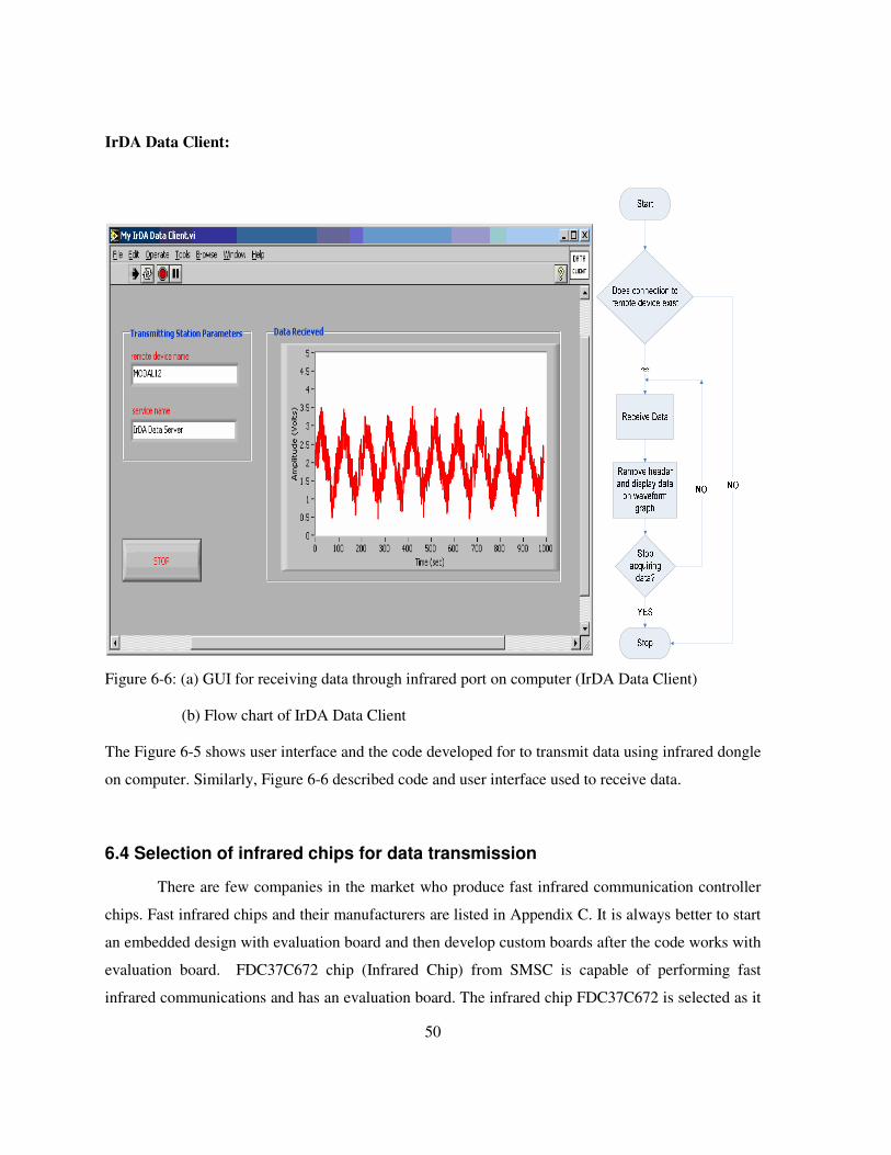
50
IrDA Data Client:
Figure 6-6: (a) GUI for receiving data through infrared port on computer (IrDA Data Client)
(b) Flow chart of IrDA Data Client
The Figure 6-5 shows user interface and the code developed for to transmit data using infrared dongle
on computer. Similarly, Figure 6-6 described code and user interface used to receive data.
6.4 Selection of infrared chips for data transmission
There are few companies in the market who produce fast infrared communication controller
chips. Fast infrared chips and their manufacturers are listed in Appendix C. It is always better to start
an embedded design with evaluation board and then develop custom boards after the code works with
evaluation board. FDC37C672 chip (Infrared Chip) from SMSC is capable of performing fast
infrared communications and has an evaluation board. The infrared chip FDC37C672 is selected as it

51
has the evaluation board EVB-SIO-672 which is fully functional. In subsequent chapters infrared
systems using the infrared chip FDC37C672 and the microcontroller PIC18F452 will be discussed.
6.5 Basic Architectures
In this chapter an introduction to the hardware architectures of infrared acquisition board is
given. In this chapter interface between the PIC microcontroller and the FDC37C672[13] and the
problems encountered will described. Initially, registers inside FDC37C672 were readable but not
writable due to some malfunctioning of interface between the PIC microcontroller and the
FDC37C672. After debugging, it was found that floating reset pin on FDC37C672 didn’t allow us to
write into registers inside FDC37C672. Once the RESET on the FDC37C672 pin was grounded, the
FDc37C672 was writable.
The PIC 18F452 was chosen to communicate with the FDC37C672 (Infrared Chip). Infrared chip
requires ISA bus from the host (microcontroller) to communicate with it. The PIC18F452 has a large
number of I/O ports. It is possible to connect the microcontroller's inputs without any sophisticated
interface logic one by one to the ISA slot. The infrared chip has an 8-bit architecture so it can be
processed with the PIC microcontroller with little overhead. In the following paragraph ISA interface
logic between the PIC microcontroller and the Infrared chip will be explained. The ISA bus protocol
is easy to implement and the 8-bit mode of the card reduces complexity of the PIC - Infrared
interface.
6.6 ISA Overview
The Industry Standard Architecture (ISA) bus originated in the early 1980’s at a development
lab in IBM. The original IBM Personal Computer introduced in 1981 included the 8-bit subset of the
ISA bus. In 1984, IBM introduced the PC-AT which was the first full 16-bit implementation of the
ISA bus. The ISA bus has
a) Data lines to move data between the host and the device in both directions. The host
(usually PC or microcontroller) controls data transfer.
b) Address lines: The host uses these lines to access Input/Output or memory addresses inside
device.
c) Control Lines: These lines are used to control direction transfer of data.

52
The infrared chip has 8 data lines (D0-D7), 11 address lines (A0-A10) and 2 control lines (nIOR and
nIOW) for ISA communication. Inorder to ensure proper communication between the PIC
microcontroller and the FDC37C672, it is important to understand read and write cycles of the ISA
bus. PIC microcontroller reads and writes data to the FDC37C672 by asserting ISA read and write
cycles. Descriptions of ISA bus read and write cycle for PIC microcontroller is given below:
Read Cycle:
a) Microcontroller sends out the address on A0-A10 lines.
b) Then the microcontroller takes the -IOR signal to a low level. Then address of the target
port to be read will be latched, so that the addressed device will take a data byte to the D0-D7
data bus.
c) The microcontroller will read then the data bus and take the -IOR signal to a high again.
Write Cycle:
a) The microcontroller outputs address on A0-A10.
b) The microcontroller sends out the data byte D0-D7 to be written.
c) It then asserts the -IOW signal.
d) After the device has time to read the data byte, the microcontroller raises the -IOW signal
high again.
6.7 Interface between infrared chip and microcontroller
In this section, pin count analysis is performed to check the compatibility of the PIC
microcontroller with the FDC37C672. The microcontroller PIC18F452 has four GPIO (general
Purpose Input Output) ports which are 8-bits wide and one GPIO port which is 4-bits wide. A total of
36 lines are available for communication. PORTA, PORTB, PORTC, PORTD and PORTE are the
GPIO ports available on the PIC Microcontroller. There are some design constraints on the number of
digital lines available from the microcontroller for this application. Since the main objective of this
project is to develop an infrared data acquisition system with 8 channels, PORTA is not used for ISA
bus communication. PORTA is used acquiring analog signals from sensor. In the 28 digital lines
available on the PIC microcontroller for ISA communication, 3 of the digital lines on PORTB are
used to debug C code on the PIC. The remaining 25 lines are available on the PIC microcontroller for
ISA communications. The interface to the infrared chip requires 8 data lines, 11 address lines and 2
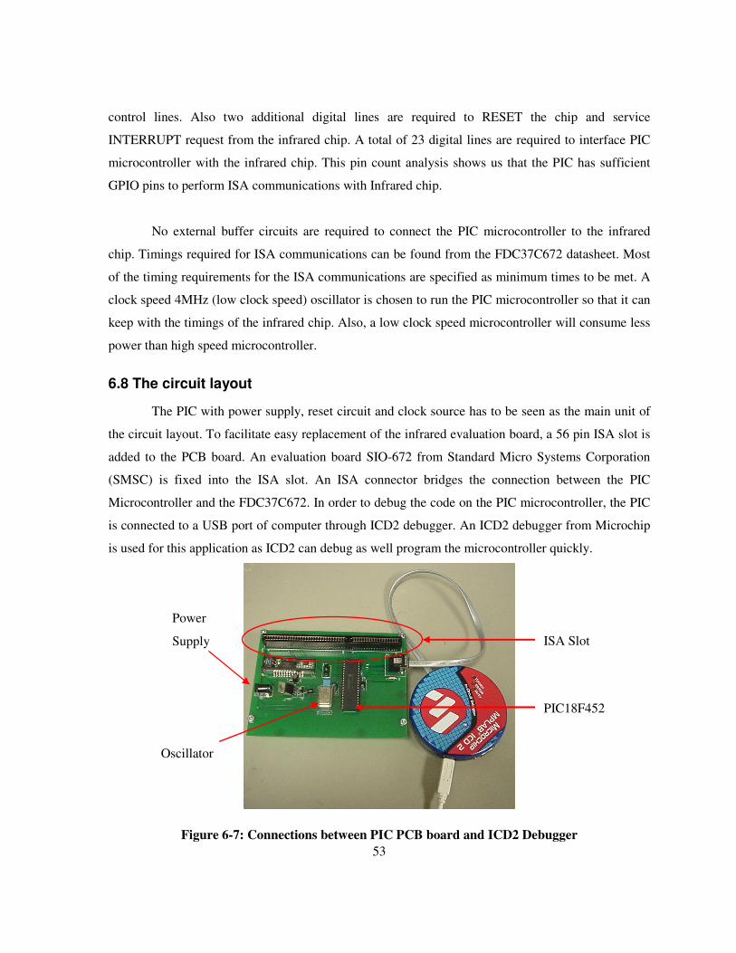
53
control lines. Also two additional digital lines are required to RESET the chip and service
INTERRUPT request from the infrared chip. A total of 23 digital lines are required to interface PIC
microcontroller with the infrared chip. This pin count analysis shows us that the PIC has sufficient
GPIO pins to perform ISA communications with Infrared chip.
No external buffer circuits are required to connect the PIC microcontroller to the infrared
chip. Timings required for ISA communications can be found from the FDC37C672 datasheet. Most
of the timing requirements for the ISA communications are specified as minimum times to be met. A
clock speed 4MHz (low clock speed) oscillator is chosen to run the PIC microcontroller so that it can
keep with the timings of the infrared chip. Also, a low clock speed microcontroller will consume less
power than high speed microcontroller.
6.8 The circuit layout
The PIC with power supply, reset circuit and clock source has to be seen as the main unit of
the circuit layout. To facilitate easy replacement of the infrared evaluation board, a 56 pin ISA slot is
added to the PCB board. An evaluation board SIO-672 from Standard Micro Systems Corporation
(SMSC) is fixed into the ISA slot. An ISA connector bridges the connection between the PIC
Microcontroller and the FDC37C672. In order to debug the code on the PIC microcontroller, the PIC
is connected to a USB port of computer through ICD2 debugger. An ICD2 debugger from Microchip
is used for this application as ICD2 can debug as well program the microcontroller quickly.
Figure 6-7: Connections between PIC PCB board and ICD2 Debugger
ISA Slot
PIC18F452
Power
Supply
Oscillator

54
A schematic between the PIC microcontroller and the ISA slot is shown in the picture below.
Schematics and board were made using Protel software, an Electronic CAD Software that runs under
Windows. A free evaluation version of Protel is used for design PCB baord, as it has a powerful auto
router for the board layout, and allows boards up to size of 100 x 80 mm.
Figure 6-8: Schematics of PIC- ISA board
A PCB board with two layers (Figure 6-9) was designed using Protel software as it is easy to
test the connections between different devices such as power supply, microcontroller and the infrared
chip on the 2 layer PCB board. In the final development system, a 4 layer board with power and
ground planes in between the top and bottom layer is to be designed.

55
Figure 6-9: Picture of Evaluation Board in ISA Slot
6.9 Infrared Communication
The FDC37C672 [13]is a super I/O chip with infrared capability. It can also be configured to
work as a UART, Floppy Disk Controller, Keyboard Controller and Parallel port device. It has an ISA
interface and is a plug and play device. FDC37C672 has 128 byte FIFO buffer. FDC37C672 can be
configured to work as Serial, Sharp-IR, SIR (IrDA 1.0), MIR and FIR (IrDA 1.1), and Consumer
Electronics IR mode. FDC37C672 is a super I/O chip with set of registers built inside the chip.
Configuring registers specific to Infrared operation will enable infrared module inside the
FDC37C672. In the next paragraph 6.9.1, configuration of the FDC37C672 to operate in Infrared
Mode is discussed.
6.9.1 Configuration
The FDC37C672 device operates in two states: (a) Run or user state (b) Configuration State.
FDC37C672 enters into configuration by writing configuration key 0x55 to configuration base
address (0x3F0h). Only after entering into configuration mode, INDEX (0x3f0h) and DATA PORT
(0x3F1h) registers become effective to configure devices. Device enters into Configuration Mode by
writing Configuration Key 0x55 (hexadecimal value 55) to CONFIG PORT after Power on Reset or
Hard Reset. The device exits configuration state and returns to normal mode when 0xAA
(hexadecimal value AA) is written to CONFIG PORT. To perform fast infrared communications
using FDC37C672, the infrared device inside FDC37C672 should enabled and powered by entering

56
into configuration mode. After configuring the FDC37C672 to operate in infrared mode, FDC37C672
can switch back to normal mode. Now, all the infrared registers can be accessed in normal mode.
6.9.1.1 Configuration Sequence
To program configuration registers, the following sequence must be followed:
1. Enter into FDC37C672 Configuration Mode
2. Configure the Configuration registers
3. Exit FDC37C672 Configuration Mode
Only two states are defined (Run and Configuration) inside FDC37C672. In the Run state
FDC37C672 will always be ready to enter the configuration state.
Table 3: Logical Device number of devices inside FDC37C672
Logical Device Number Logical Device
Logical Device 0 Floppy Disk Device
Logical Device 1 Reserved
Logical Device 2 Reserved
Logical Device 3 Parallel Port
Logical Device 4 Serial Port 1
Logical Device 5 Serial Port 2
Logical Device 6 Reserved
Logical Device 7 Keyboard
Logical Device 8 Auxiliary I/O
Logical Device 9 Reserved
The Table 3 above shows logical device numbers associated with the different logical
devices. Serial Port 2 can be configured to work in either UART mode or Infrared Mode. UART 2 of
the FDC37C672 is intended for infrared communication. It provides three different units, one for the
original IrDA standard for speeds up to 115200 baud (referred to as SIR mode in the following),
1.152 Mbps (MIR) and 4.0Mbps standard (referred to as FIR mode). Both units have a distinct set of
control registers, but they share the same pins for transmission/receiving data and interrupt control as
a result they cannot be operated at the same time. Each unit consists of a bit encoder/decoder and a

57
serial to parallel data engine. The SIR mode is based on a UART (UART 2) while the engine for the
high speed mode is a high speed serial to parallel (HSSP) receiver-transmitter. To support a variety of
IrDA transceivers, transmit and receive data pins can be configured to use either normal or inverted
data. Transmit and receive polarity depends on the infrared transceiver used for infrared
communications. The pins are designed to be directly connected to the infrared transceiver modules.
Figure 6-10: Infrared Communication Controller Components
To operate the FDC37C672 in Infrared Mode, Logical Device 5 should be accessed by
entering configuration mode. Logical Device 5 is configured to work in IrDA mode instead of
UART2 Mode.
Logical Device 5 is enabled, powered and set to work in Fast Infrared Mode. The code for performing
these steps in PIC Microcontroller is added in Appendix B under the function smc_init_chip ( ).
6.9.2 Checking the connection between Infrared Device and PIC Microcontroller
FDC37C672 has two registers which are specific to the device which are written by the
manufacturer at the time of manufacturing. The registers are only readable by the user. Reading these
registers (Device ID and Device Rev) and checking the value with the value supplied in datasheet
indicates the presence of FDC37C672.

58
Table 4: Device Identification registers inside FDC37C672
Register Number Register Name Value
0x21 Device ID 0x40
0x22 Device Rev 0x01
Chip detection is also included in the code for smc_init_chip ( ).
6.10 Loop Back Test for Fast Infrared Communication
As explained above, the fast infrared base I/O Address is set as 0x300h. After exiting from
configuration mode, all the fast infrared registers can be accessed with offset to this address (0x300).
Before configuring fast infrared module, it is necessary to make sure that the fast infrared module is
accessed correctly. Registers in fast infrared module are arranged in pages or banks. In order to access
some specific registers associated with fast infrared modules, banks should be switched. Registers are
formatted in banks to save addressing space in the chip. The infrared module inside FDC37C672 has
two IrCC 2.0 [15]Block Identifier Registers (see Table 5). These read-only registers classify hardware
manufacture, the Device ID, the Version Number and Host Interface Parameters.
Table 5: Device Identification registers of Infrared Block (IrCC 2.0) inside FDC37C672
Register Number Register Name Value
0x0 (Block 3) SMSC ID (high-byte) 0x10
0x1 (Block 3) SMSC ID (low-byte) 0xB8
0x2 (Block 3) CHIP ID 0xF2
0x3 (Block 3) VERSION Number 0x00
SMSC ID registers (show in Table 5) are 16 bit manufacturer identification code. These Chip ID
register identify Infrared Module inside FDC37C672. Reading these IrCC 2.0 identification registers
and checking the value with the value supplied in datasheet indicates the presence of IrCC 2.0.
After IrCC 2.0 is identified, a loop back test is done. The loop back test should always be
performed on the FDC37C672 before setting up infrared link. This test ensures that all components are
functioning properly and thus assuring a reliable connection. The loop back test is performed on the fast
infrared module inside FDC37C672 to check the functionality of fast infrared communications. The

59
loop back mode allows diagnostic of the Fast Infrared Infrared Module. Once the Infrared module
passes the loop back test it indicates that fast infrared module is capable of performing fast infrared
communications. This allows indicates that the code and hardware developed for fast infrared
communication is fully-functional. After this step, data from the fast infrared chip can be transferred to
the Infrared Transceiver and transmitted in Infrared Medium. On FDC37C672 an internal loop back
facility is available. So, an internal loop back test is done. With the external loop back test, data will be
transmitted at the same time. Fast infrared communication is half duplex, which means data cannot be
received and transmitted at the same time. Since it is not possible to perform the external loop back test,
the internal loop back test is done. Loop back tests require that Infrared Module FIFO be used for both
transmit and receive modes, simultaneously. In fast infrared module, receiver and transmitter share
same FIFO as fast infrared module operates in half-duplex mode. So, in loop back mode data is to be
transmitted first and then loop back mode should be enabled.
Figure 6-11: IrDA FIR encoder inside FDC37C672
The code for the above operation is in the function smc_chip_loop_back( ).

60
Chapter 7
Conclusion
Introduction of the miniature wireless electrophysiology instrumentation would greatly aid
memory research. Unfortunately, wireless technology is somewhat limited in bandwidth and range,
which sometimes offsets its inherent benefits. Also, power is one of big issues with wireless
technologies. This thesis presented a RF wireless system to transmit neural signals. A RF system
couldn’t achieve the higher sampling rates required but provided a reliable RF wireless connection to
replace a wired system. A fast infrared system was developed to replace the RF system. The infrared
system provides higher bandwidth but limited in its range. For application in hand, range is not a
concern. Thus short range infrared technology promising and a more viable alternative to wired
systems.
This proof-of-concept RF system was constructed using inexpensive commercially available
electronic components. A Microchip PIC MCU was used for analog to digital conversion and to
communicate with the ML2724 Starter Kit. The PIC18F452 MCU and its C code were described in
detail. Also described was the ML2724 Starter Kit module. Bluetooth protocol and frequency
hopping was discussed not because these concepts were needed to implement the module, but because
these concepts were needed to appreciate the module, as its simplicity is deceptive. The PIC code
written for the PIC18F452 device was demonstrated to work properly, and the performance of the RF
wireless data acquisition system transceiver was measured.
It was shown that some data was lost over the radio frequency link during uninterrupted
transmission in continuous mode. Possible reasons for the lost data were given and some future work
was suggested for improving the prototype device.
An infrared system is developed which can operate in the loop back mode. The PIC MCU
collects data from sensor and communicates with the FDC37C672. The fast infrared communication
is discussed in detail as it is required to properly configure the FDC37C672. The C code written for
PIC MCU to operate fast infrared module inside FDC37C672 is functional and tested. Future work
required for fully functional infrared link is discussed. As electronics continue to become
miniaturized and wireless technology improves, as it inevitably will, the applications for wireless
technology will undoubtedly proliferate.

61
Appendix A
PIC C Code for RF Transmission
/*********************************************************************
Filename:test_adc.c
Main Program
PIC Used- PIC 18f452
Oscillator Clock Speed - 40MHz
Baud Rate - 57600
Transmit Buffer Size -16
Receive Buffer Size - 16
Additional Files Required:
test_adc.c
USRTInt.c
UARTInt.h
UARTIntC.def
18f452i.lkr
*************************************************************************/
#include "UARTIntC.h"
#include "delays.h"
#include <p18f452.h>
/*Extra Headers*/
#include "adc.h"
#include "delays.h"
void low_isr(void);
// serial interrupt taken as low priority interrupt
#pragma code uart_int_service = 0x08
void uart_int_service(void) _asm goto low_isr _endasm
#pragma code
#pragma interruptlow low_isr save=section(".tmpdata")

62
void low_isr(void)
// call of library module function, MUST
UARTIntISR();
void main(void)
// Test data array
unsigned char spArray[]='A','T','+','X','C','E','N','=','1','\r','\n';
unsigned char j = 0,i=0,l=0,k=0;
unsigned char TX_ZERO = 0,chData,chData1;
// Initalize UART Module
UARTIntInit();
// configure A/D convertor
OpenADC( ADC_FOSC_8 & ADC_RIGHT_JUST & ADC_8ANA_0REF,
ADC_CH0 & ADC_INT_OFF);
// Just to show that PIC is working
TRISB=0x0;
PORTB=0x03;
//WDTCONbits.SWDTEN=0x0;
//Enable ML2724 Transceiver by transmitting AT+XCEN=1 command to ML2724
k=0;
While (k<11)
if (UARTIntPutChar(spArray[k])) k++;
Delay1KTCYx (60); //Delay of 15ms to charge up charge amplifier
// Display data acquired on PORTB
PORTB=0xff;
// Start Continuous data acquisition
while (1)
Delay1KTCYx (22); //Delay of 15ms

63
ConvertADC(); // Start conversion
While (BusyADC() ) // Wait for completion
if (i==0)
if (TX_ZERO==0)
// Transmit AT Command before sending packet
UARTIntPutChar('A'); UARTIntPutChar('T'); UARTIntPutChar('+');
UARTIntPutChar('C'); UARTIntPutChar('H'); UARTIntPutChar('A');
UARTIntPutChar('T'); UARTIntPutChar('='); TX_ZERO=1;
else TX_ZERO=0;
chData=ADRESL; chData1=ADRESH;
//Transmit Lower Byte
if(!chData) UARTIntPutChar(0x1);
else if(chData=='\r') UARTIntPutChar(0x0E);
else UARTIntPutChar(chData);
//Transmit Upper Byte
//Increment chData1 to eliminate \0 termination error. Later it will be decoded in reception program
UARTIntPutChar(++chData1);
PORTB=chData;
//Transmit Termination Character
if(i++>=32)
UARTIntPutChar('\r'); UARTIntPutChar('\n'); i=0;
//Close A/D Converter
CloseADC();

64
/*********************************************************************
* This file implements the functionality of UART with user defined circular buffer. It has the
* implementation of functions namely UARTIntPutChar, UARTIntGetChar and UARTIntISR .
* These functions are the core part of UART MPAM module. Additional functions will be
* added in future as more desired functionality is identified.
*********************************************************************
* FileName: UARTIntC.C
* Dependencies: UARTIntC.h
* Processor: PIC18XXX
* Compiler: MCC18
* Assembler: MPASMWIN 03.20.07
* Linker: MPLINK 3.20
* Company: Microchip Technology, Inc.
********************************************************************/
#include "UARTIntC.h"
#include <p18f452.h>
// status flags of receive and transmit buffers
struct status vUARTIntStatus;
// variable definitions
#if TXON
unsigned char vUARTIntTxBuffer[TX_BUFFER_SIZE];
unsigned char vUARTIntTxBufDataCnt;
unsigned char vUARTIntTxBufWrPtr;
unsigned char vUARTIntTxBufRdPtr;
#endif
#if RXON
unsigned char vUARTIntRxBuffer[RX_BUFFER_SIZE];
unsigned char vUARTIntRxBufDataCnt;
unsigned char vUARTIntRxBufWrPtr;

65
unsigned char vUARTIntRxBufRdPtr;
#endif
/*********************************************************************
* Function: void UARTIntInit(void)
* PreCondition: None
* Input: None
* Output: None
* Side Effects: None
* Stack Requirements: 1 level deep
* Overview: This function initializes UART peripheral. This function need to be called before
*using UARTIntPutChar and UARTIntGetChar functions to send and receive the characters.
********************************************************************/
void UARTIntInit(void)
// Initializing the status variables and circular buffer variables.
#if TXON
vUARTIntStatus.UARTIntTxBufferFull = 0;
vUARTIntStatus.UARTIntTxBufferEmpty = 1;
vUARTIntTxBufDataCnt = 0;
vUARTIntTxBufWrPtr = 0;
vUARTIntTxBufRdPtr = 0;
#endif
#if RXON
vUARTIntStatus.UARTIntRxBufferFull = 0;
vUARTIntStatus.UARTIntRxBufferEmpty = 1;
vUARTIntStatus.UARTIntRxError = 0;
vUARTIntStatus.UARTIntRxOverFlow = 0;
vUARTIntRxBufDataCnt = 0;
vUARTIntRxBufWrPtr = 0;
vUARTIntRxBufRdPtr = 0;
#endif
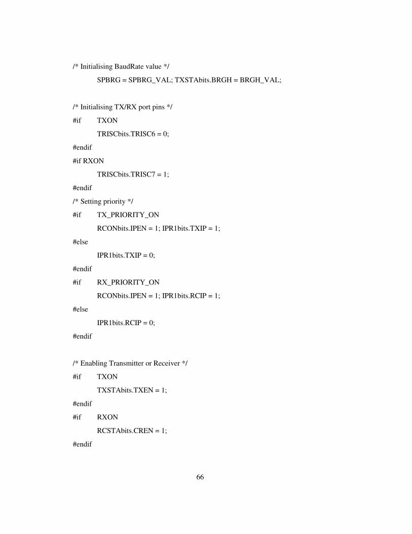
66
/* Initialising BaudRate value */
SPBRG = SPBRG_VAL; TXSTAbits.BRGH = BRGH_VAL;
/* Initialising TX/RX port pins */
#if TXON
TRISCbits.TRISC6 = 0;
#endif
#if RXON
TRISCbits.TRISC7 = 1;
#endif
/* Setting priority */
#if TX_PRIORITY_ON
RCONbits.IPEN = 1; IPR1bits.TXIP = 1;
#else
IPR1bits.TXIP = 0;
#endif
#if RX_PRIORITY_ON
RCONbits.IPEN = 1; IPR1bits.RCIP = 1;
#else
IPR1bits.RCIP = 0;
#endif
/* Enabling Transmitter or Receiver */
#if TXON
TXSTAbits.TXEN = 1;
#endif
#if RXON
RCSTAbits.CREN = 1;
#endif

67
/* Enabling Serial Port */
RCSTAbits.SPEN = 1;
/* Enable the TX and RX. Interrupt */
#if TXON
PIE1bits.TXIE = 1;
#endif
#if RXON
PIE1bits.RCIE = 1;
#endif
/* Setting Global interrupt pins */
#if ((TX_PRIORITY_ON)|(RX_PRIORITY_ON))
INTCONbits.GIEH = 1; INTCONbits.GIEL = 1;
#else
INTCONbits.GIE = 1; INTCONbits.PEIE = 1;
#endif
/*********************************************************************
* Function: unsigned char UARTIntPutChar(unsigned char)
* PreCondition: UARTIntInit()function should have been called.
* Input: unsigned char
* Output: unsigned char
* 0 - single character is successfully added to transmit buffer. 1 - Transmit buffer is full and the
* character could not be added to transmit buffer.
* Side Effects: None
* Stack Requirements: 1 level deep
* Overview: This function puts the data in to transmit buffer. Internal implementation wise , it
*places the argument data in transmit buffer and updates the data count and write pointer variables.
*********************************************************************/

68
#if TXON
unsigned char UARTIntPutChar(unsigned char chCharData)
/* check if its full , if not add one */ /* if not busy send data */
if(vUARTIntStatus.UARTIntTxBufferFull) return 0;
//critical code , disable interrupts
PIE1bits.TXIE = 0; vUARTIntTxBuffer[vUARTIntTxBufWrPtr] = chCharData;
vUARTIntStatus.UARTIntTxBufferEmpty = 0; vUARTIntTxBufDataCnt ++;
if(vUARTIntTxBufDataCnt == TX_BUFFER_SIZE)
vUARTIntStatus.UARTIntTxBufferFull = 1;
vUARTIntTxBufWrPtr++;
if(vUARTIntTxBufWrPtr == TX_BUFFER_SIZE)
vUARTIntTxBufWrPtr = 0;
PIE1bits.TXIE = 1;
return 1;
/*********************************************************************
* Function: unsigned char UARTIntGetTxBufferEmptySpace(void)
* PreCondition: UARTIntInit()function should have been called.
* Input: None
* Output: unsigned char
* 0 - There is no empty space in transmit buffer. number - the number of bytes of empty
* space in transmit buffer.
* Side Effects: None
* Stack Requirements: 1 level deep
* Overview: This function returns the number of bytes of free space left out in the transmit
*buffer at the calling time of this function. It helps the user to further write data in to transmit
* buffer at once, rather than checking transmit buffer is full or not with every addition of
* data in to the transmit buffer.
********************************************************************/

69
unsigned char UARTIntGetTxBufferEmptySpace(void)
if(vUARTIntTxBufDataCnt < TX_BUFFER_SIZE)
return(TX_BUFFER_SIZE-vUARTIntTxBufDataCnt);
else return 0;
#endif
/*********************************************************************
* Function: unsigned char UARTIntGetChar(unsigned char*)
* PreCondition: UARTIntInit()function should have been called.
* Input: unsigned char*
* Output: unsigned char
* 0 - receive buffer is empty and the character could not be read from the receive buffer.
* 1 - single character is successfully read from receive buffer.
* Side Effects: None
* Stack Requirements: 1 level deep
* Overview: This function reads the data from the receive buffer. It places the data in
* argument and updates the data count and read pointer variables of receive buffer.
********************************************************************/
#if RXON
unsigned char UARTIntGetChar(unsigned char *chTemp)
if( vUARTIntStatus.UARTIntRxBufferEmpty) return 0;
//critical code, disabling interrupts here keeps the access pointer values proper.
PIE1bits.RCIE = 0; vUARTIntStatus.UARTIntRxBufferFull = 0;
*chTemp = vUARTIntRxBuffer[vUARTIntRxBufRdPtr]; vUARTIntRxBufDataCnt--;
if(vUARTIntRxBufDataCnt == 0 ) vUARTIntStatus.UARTIntRxBufferEmpty = 1;
vUARTIntRxBufRdPtr++;
if(vUARTIntRxBufRdPtr == RX_BUFFER_SIZE) vUARTIntRxBufRdPtr = 0;
PIE1bits.RCIE = 1; return 1;

70
/*********************************************************************
* Function: unsigned char UARTIntGetRxBufferDataSize(void)
* PreCondition: UARTIntInit()function should have been called.
* Input: None
* Output: unsigned char
* number - the number of bytes of data in receive buffer.
* Side Effects: None
* Stack Requirements: 1 level deep
* Overview: This function returns the number of bytes of data available in receive buffer
* at the calling time of this function. It helps the user to read data from receive buffer at
* once rather than checking receive buffer is empty or not with every read of data from
* receive buffer.
********************************************************************/
unsigned char UARTIntGetRxBufferDataSize(void)
return vUARTIntRxBufDataCnt;
#endif
/*********************************************************************
* Function: void UARTIntISR(void)
* PreCondition: UARTIntInit() function should have been called.
* Input: None
* Output: None
* Side Effects: None
* Stack Requirements: 2 level deep
* Overview: This is the Interrupt service routine which is called in the user application's
* ISR portion. This function actually sends the data from transmit buffer to USART and updates
* the data count and read pointer variables of transmit buffer. For the receive portion, it reads the
* data from USART and places the data in to receive buffer (if no errors occured) and updates data
* count and write pointer variables receive buffer. If the receive buffer is full and it receives more
* data error flag is set.If frame errors(FERR) occur it sets the error flag. If over flow errors(OERR)

71
* occurs, it clears and sets the CREN bit, so that USART can receive further data.
********************************************************************/
void UARTIntISR(void)
#if RXON unsigned char chTemp; #endif
#if TXON
if(PIR1bits.TXIF & PIE1bits.TXIE)
if(!vUARTIntStatus.UARTIntTxBufferEmpty)
TXREG = vUARTIntTxBuffer[vUARTIntTxBufRdPtr];
if(vUARTIntStatus.UARTIntTxBufferFull)
vUARTIntStatus.UARTIntTxBufferFull = 0;
vUARTIntTxBufDataCnt--;
if(vUARTIntTxBufDataCnt == 0)
vUARTIntStatus.UARTIntTxBufferEmpty = 1;
vUARTIntTxBufRdPtr++;
if(vUARTIntTxBufRdPtr == TX_BUFFER_SIZE)
vUARTIntTxBufRdPtr = 0;
Else PIE1bits.TXIE = 0;
#endif
#if TXON_AND_RXON
else if( PIR1bits.RCIF & PIE1bits.RCIE)
#elif TXOFF_AND_RXON
if( PIR1bits.RCIF & PIE1bits.RCIE)
#endif
#if RXON if(RCSTAbits.FERR) /* FERR error condition */
chTemp = RCREG; vUARTIntStatus.UARTIntRxError = 1;
else if (RCSTAbits.OERR) /* OERR error condition */
RCSTAbits.CREN = 0; RCSTAbits.CREN = 1;
chTemp = RCREG; vUARTIntStatus.UARTIntRxError = 1;
else if ( vUARTIntStatus.UARTIntRxBufferFull)

72
chTemp = RCREG;
vUARTIntStatus.UARTIntRxOverFlow = 1;
else if(!vUARTIntStatus.UARTIntRxBufferFull)
vUARTIntStatus.UARTIntRxOverFlow = 0;
vUARTIntStatus.UARTIntRxBufferEmpty = 0;
vUARTIntRxBuffer[vUARTIntRxBufWrPtr] = RCREG;
vUARTIntRxBufDataCnt ++;
if(vUARTIntRxBufDataCnt == RX_BUFFER_SIZE)
vUARTIntStatus.UARTIntRxBufferFull = 1; vUARTIntRxBufWrPtr++;
if(vUARTIntRxBufWrPtr == RX_BUFFER_SIZE) vUARTIntRxBufWrPtr = 0;
#endif

73
/*********************************************************************
* This file implements the library functionality of UART. It adds Transmit and receive functionality,
* circular buffer and interrupt functionality.
*********************************************************************
* FileName: UARTIntC.h
* Dependencies: UARTIntC.def
* Processor: PIC18XXX
* Compiler: MCC18
* Assembler: MPASMWIN 03.20.07
* Linker: MPLINK 3.20
* Company: Microchip Technology, Inc.
********************************************************************/
#ifndef _UARTIntC_H
#define _UARTIntC_H
#include "UARTIntC.def"
/* Constants found in .def file are given readable names*/
#define TX_BUFFER_SIZE UARTINTC_TX_BUFFER_SIZE
#define RX_BUFFER_SIZE UARTINTC_RX_BUFFER_SIZE
#ifdef UARTINTC_TXON
#define TXON 1
#elif UARTINTC_TXOFF
#define TXON 0
#endif
#ifdef UARTINTC_RXON
#define RXON 1
#elif UARTINTC_RXOFF
#define RXON 0
#endif

74
#define TXON_AND_RXON ((TXON) & (RXON))
#define TXOFF_AND_RXON ((!(TXON)) & (RXON))
// User can change the following values and accordingly
// the ISR location in the main application.
// Can they be MPAM module parameters?
#define BRGH_VAL 1
#define TX_PRIORITY_ON 0
#define RX_PRIORITY_ON 0
// More error check to be done and the following
// code can be modified.
// If SPBRG is out of range, it won't let the
// main application be compiled and linked.
#define SPBRG_V1 (UART_CLOCK_FREQ / UARTINTC_BAUDRATE)
#define SPBRG_V2 SPBRG_V1/16
#define SPBRG_VAL (SPBRG_V2 - 1)
# if (SPBRG_VAL > 255)
#error Calculated SPBRG value is out of range
#elif (SPBRG_VAL < 10)
#error Calculated SPBRG value is out of range
#endif
struct status
unsigned UARTIntTxBufferFull :1; unsigned UARTIntTxBufferEmpty :1;
unsigned UARTIntRxBufferFull :1; unsigned UARTIntRxBufferEmpty :1;
unsigned UARTIntRxOverFlow :1; unsigned UARTIntRxError:1; ;
extern struct status vUARTIntStatus;
// variables representing status of transmission buffer and
// transmission buffer it self are declared below

75
#if TXON
extern unsigned char vUARTIntTxBuffer[TX_BUFFER_SIZE];
extern unsigned char vUARTIntTxBufDataCnt;
extern unsigned char vUARTIntTxBufWrPtr;
extern unsigned char vUARTIntTxBufRdPtr;
#endif
// variables referring the status of receive buffer.
#if RXON
extern unsigned char vUARTIntRxBuffer[RX_BUFFER_SIZE];
extern unsigned char vUARTIntRxBufDataCnt; extern unsigned char vUARTIntRxBufWrPtr;
extern unsigned char vUARTIntRxBufRdPtr;
#endif
// functions offered by this module
#if RXON
// function returns a character from receive buffer
unsigned char UARTIntGetChar(unsigned char*);
// function returns the number of characters in receive buffer
unsigned char UARTIntGetRxBufferDataSize(void);
#endif
#if TXON
// function to put a character in Transmit buffer
unsigned char UARTIntPutChar(unsigned char);
// function returns size of the empty section of Transmit buffer
unsigned char UARTIntGetTxBufferEmptySpace(void);
#endif
// Initialization of the module
void UARTIntInit(void);
// Interrupt service routine supplied by the module. This need to be

76
// called from ISR of the main program.
void UARTIntISR(void);
// Other useful macros
#define mDisableUARTTxInt() PIE1bits.TXIE = 0
#define mEnableUARTTxInt() PIE1bits.TXIE = 1
#define mDisableUARTRxInt() PIE1bits.RCIE = 0
#define mEnableUARTRxInt() PIE1bits.RCIE = 1
#define mSetUARTRxIntHighPrior() \
RCONbits.IPEN = 1;\ IPR1bits.RCIP = 1
#define mSetUARTRxIntLowPrior() IPR1bits.RCIP = 0
#define mSetUARTTxIntHighPrior()\ RCONbits.IPEN = 1;\ IPR1bits.TXIP = 1
#define mSetUARTTxIntLowPrior() IPR1bits.TXIP = 0
#define mSetUART_BRGHHigh() TXSTAbits.BRGH = 1
#define mSetUART_BRGHLow() TXSTAbits.BRGH = 0
#define mSetUART_SPBRG(iBRGValue)\ RCSTAbits.SPEN = 0;\
SPBRG = iBRGValue;\ RCSTAbits.SPEN = 1
#define mSetUARTBaud(iBaudRate)\ do\
#define SPBRG_V11 (UART_CLOCK_FREQ / UARTINTC_BAUDRATE)\
#define SPBRG_V21 SPBRG_V11/16\
#define SPBRG_VAL (SPBRG_V21 - 1)\
#if (SPBRG_VAL > 255)\
#error Calculated SPBRG value is out of range\
#elif (SPBRG_VAL < 10)\
#error Calculated SPBRG value is out of range\
#endif\
RCSTAbits.SPEN = 0;\
SPBRG = iBaudRate;\
RCSTAbits.SPEN = 1;\
while(false)

77
//###########################################################################
//UARTIntC.def
//This file is generated by Microchip Application Maestro
//DO NOT MODIFY MANUALLY
//###########################################################################
#ifndef _UARTIntC_DEF
#define _UARTIntC_DEF
#ifndef UART_CLOCK_FREQ
#define UART_CLOCK_FREQ 40000000
#endif
#define UARTINTC_TXON
#define UARTINTC_RXON
#define UARTINTC_BAUDRATE 57600
#define UARTINTC_TX_BUFFER_SIZE 16
#define UARTINTC_RX_BUFFER_SIZE 16
#endif

78
Appendix B
Table below shows list of manufactures producing devices with infrared capability with part numbers.
Manufacturer Type Part Number
National IR Controller PC87108
IR Controller PC87109
Super I/O PC87308
Super I/O PC87338
Super I/O PC97338
SMSC Super I/O FDC37C672
Super I/O FDC37C669
Super I/O LPC47N227
IR Controller CAM35C44
Winbond Super I/O W83877AF
Super I/O W83977AF
TI Communication Peripherals TIR2000
IBM Communication Peripherals 31T5102

79
Bibliography
[1] John B.Peatman. 2002, Embedded Design with the PIC18F452, Prentice Hall [2] Maxim, Introduction to Direct-Sequence Spread-Spectrum Communications,
http://www.maxim-ic.com/appnotes.cfm/appnote_number/1890
[3] Ian Miller, M.B., Bryan J Doohogue, Kirk W.Lindstorm, Stuart Williams. Standard for High
Speed Infrared Communications, http://www.findarticles.com/p/articles/mi_m0HPJ/is_n1_v49/ai_20329859.
[4] Microchip, PIC18F452: Compatible 10-Bit Analog-To-Digital (A/D) Converter Module.
[5] Maxim, ML2724 Starter Kit, http://www.microlinear.com/downloads/PB/PB_ML_SK02.pdf [6] Maxim, ML2724 Transceiver Datasheet, www.microlinear.com
[7] Microchip, MCC18 C compiler User’s Guide,
ww1.microchip.com/downloads/en/DeviceDoc/MPLAB_C18_Users_Guide_51288d.pdf [8] Microchip, PIC18F452 Microcontroller Datasheet,
http://ww1.microchip.com/downloads/en/DeviceDoc/39564b.pdf
[9] SigmaTel, STIr 4200 USB/IrDA Bridge Controller, http://www.sigmatel.com/documents/stir4200-pb-4-0.pdf
[10] Texas Instrument, TIR2000: High-Speed Serial Infrared Controller with 64-Byte FIFO,
http://pdf.alldatasheet.com/datasheet-pdf/view/28764/TI/TIR2000.html
[11] Standard Microsystems Corp, FDC37C672 Enhanced Super I/O Controller with Fast IR.
http://www.smsc.com/main/datasheets/37c672.pdf [12] Standard Microsystems Corp, Infrared Communications Controller,
http://www.smsc.com/main/datasheets/ircc20.pdf [13] ISA Bus Technical Summary, http://www.techfest.com/hardware/bus/isa.htm [14] Microchip, PIC18F452 Microcontroller Datasheet,
http://ww1.microchip.com/downloads/en/DeviceDoc/39564b.pdf
[15] Franklin, C., How Bluetooth Works, www.howstuffworks.com [16] Nadel, Lynn, Cooper, Lynn A., Culicover, Peter, Harnish, R. Michael, editors, Neural
Connections, Mental Computation, The MIT Press, 1989.

80
[17] Eric Slominski, A Prototype Device for Isolating and Wirelessly Transmitting Neural Action
Potential