Embed Size (px)
Citation preview

Rochester Institute of Technology Rochester Institute of Technology
RIT Scholar Works RIT Scholar Works
Theses
12-2018
The Design and Verification of a Synchronous First-In First-Out The Design and Verification of a Synchronous First-In First-Out
(FIFO) Module Using System Verilog Based Universal Verification (FIFO) Module Using System Verilog Based Universal Verification
Methodology (UVM) Methodology (UVM)
Vinoth Nagarajan [email protected]
Follow this and additional works at: https://scholarworks.rit.edu/theses
Recommended Citation Recommended Citation Nagarajan, Vinoth, "The Design and Verification of a Synchronous First-In First-Out (FIFO) Module Using System Verilog Based Universal Verification Methodology (UVM)" (2018). Thesis. Rochester Institute of Technology. Accessed from
This Master's Project is brought to you for free and open access by RIT Scholar Works. It has been accepted for inclusion in Theses by an authorized administrator of RIT Scholar Works. For more information, please contact [email protected].
The Design and Verification of a
Synchronous First-In First-Out (FIFO) module using
SystemVerilog based Universal Verification Methodology (UVM)
byVinoth Nagarajan
Graduate PaperSubmitted in partial fulfillment
of the requirements for the degree ofMaster of Science
in Electrical Engineering
Approved by:
Mr. Mark A. Indovina, LecturerGraduate Research Advisor, Department of Electrical and Microelectronic Engineering
Dr. Sohail A. Dianat, ProfessorDepartment Head, Department of Electrical and Microelectronic Engineering
Department of Electrical and Microelectronic EngineeringKate Gleason College of Engineering
Rochester Institute of TechnologyRochester, New York
December 2018

I would like to dedicate this work to my father ’Nagarajan’, my mother ’Shanthi’, and
friends, for all of their support and encouragement throughout my career at Rochester
Institute of Technology

Abstract
With the conventional directed testbench, it is highly improbably to handle verification of
current complex Integrated Circuit (IC) designs, because a person has to manually create
every test case. The greater the complexity of the designs, the higher the probability of bugs
appearing in the code. Increasing complexity of ICs has created a necessity for performing
verification on designs with an advanced, automated verification environment. Ideally this
would eliminate chip re-spins, minimizing the time required to enable checking of all the
design specifications, ensuring 100% functional coverage. This paper deals with the design
of Synchronous FIFO using Verilog. A FIFO (First-In-First-Out) is a memory queue, which
controls the data flow between two modules. It has control logic embedded with it, which
efficiently manages read and write operations. It has the capability to notify the concerned
modules regarding its empty status and full status to help ensure no underflow or overflow
of data. This FIFO design is classified as synchronous, as clocks control the read and write
operations. Both read and write operations happen simultaneously using of Dual port
RAM or an array of flip-flops in the design. After designing the Synchronous FIFO, its
verification is carried out using the Universal Verification Methodology (UVM). A detailed
discussion about the verification plan and test results is included.

Declaration
I hereby declare that all the work and contents of this paper are original, except where
specific references are made to the work of others. They have not been submitted in part
or in whole for consideration for any other qualification or degree in this, or any other
University. This research work on the Synchronous FIFO module is the result of my own
work and includes nothing done in collaboration, except where specifically mentioned in
the text.
Vinoth Nagarajan
December 2018

Acknowledgements
I would like to thank my project advisor, professor Mark A. Indovina, for all of his support,
guidance and encouragement throughout the project. He is the sole reason for my successful
completion of this graduate paper.

Contents
Abstract ii
Declaration iii
Acknowledgements iv
Contents v
List of Figures ix
List of Tables x
1 Introduction 11.1 Need for SystemVerilog . . . . . . . . . . . . . . . . . . . . . . . . . . . . 11.2 Problems in Synchronizing circuits . . . . . . . . . . . . . . . . . . . . . . 2
1.2.1 First-in First-out (FIFO) Module . . . . . . . . . . . . . . . . . . . 21.3 Research goals . . . . . . . . . . . . . . . . . . . . . . . . . . . . . . . . . . 31.4 Contributions . . . . . . . . . . . . . . . . . . . . . . . . . . . . . . . . . . 41.5 Organization . . . . . . . . . . . . . . . . . . . . . . . . . . . . . . . . . . 4
2 Bibliographical Research 62.1 Synchronous FIFO . . . . . . . . . . . . . . . . . . . . . . . . . . . . . . . 6
2.1.1 Architecture [1] . . . . . . . . . . . . . . . . . . . . . . . . . . . . . 72.1.2 Implementation (Design and Verification) . . . . . . . . . . . . . . 8
2.2 Coverage-Driven Verification (CDV) . . . . . . . . . . . . . . . . . . . . . . 82.3 Assertion-based Verification (ABV) . . . . . . . . . . . . . . . . . . . . . . 9
3 Universal Verification Methodology (UVM) 113.1 Brief Overview - Verification Components . . . . . . . . . . . . . . . . . . 11
3.1.1 Transaction . . . . . . . . . . . . . . . . . . . . . . . . . . . . . . . 123.1.2 Sequencer . . . . . . . . . . . . . . . . . . . . . . . . . . . . . . . . 123.1.3 Driver . . . . . . . . . . . . . . . . . . . . . . . . . . . . . . . . . . 12

Contents vi
3.1.4 Monitor . . . . . . . . . . . . . . . . . . . . . . . . . . . . . . . . . 133.1.5 Agent . . . . . . . . . . . . . . . . . . . . . . . . . . . . . . . . . . 143.1.6 Environment . . . . . . . . . . . . . . . . . . . . . . . . . . . . . . 14
3.2 UVM Transaction-Level Modeling (TLM) Protocol . . . . . . . . . . . . . 143.3 UVM Phases . . . . . . . . . . . . . . . . . . . . . . . . . . . . . . . . . . 15
3.3.1 Build phase . . . . . . . . . . . . . . . . . . . . . . . . . . . . . . . 153.3.1.1 Build . . . . . . . . . . . . . . . . . . . . . . . . . . . . . 163.3.1.2 Connect . . . . . . . . . . . . . . . . . . . . . . . . . . . 163.3.1.3 end_of_elaboration . . . . . . . . . . . . . . . . . . . . . 16
3.3.2 Run-Time Phase . . . . . . . . . . . . . . . . . . . . . . . . . . . . 163.3.2.1 start_of_simulation . . . . . . . . . . . . . . . . . . . . . 163.3.2.2 Run . . . . . . . . . . . . . . . . . . . . . . . . . . . . . . 173.3.2.3 pre_reset . . . . . . . . . . . . . . . . . . . . . . . . . . . 173.3.2.4 Reset . . . . . . . . . . . . . . . . . . . . . . . . . . . . . 173.3.2.5 post_reset . . . . . . . . . . . . . . . . . . . . . . . . . . 173.3.2.6 pre_configure . . . . . . . . . . . . . . . . . . . . . . . . 173.3.2.7 Configure . . . . . . . . . . . . . . . . . . . . . . . . . . . 173.3.2.8 post_configure . . . . . . . . . . . . . . . . . . . . . . . . 183.3.2.9 pre_main . . . . . . . . . . . . . . . . . . . . . . . . . . . 183.3.2.10 Main . . . . . . . . . . . . . . . . . . . . . . . . . . . . . 183.3.2.11 post_main . . . . . . . . . . . . . . . . . . . . . . . . . . 183.3.2.12 pre_shutdown . . . . . . . . . . . . . . . . . . . . . . . . 183.3.2.13 Shutdown . . . . . . . . . . . . . . . . . . . . . . . . . . . 183.3.2.14 post_shutdown . . . . . . . . . . . . . . . . . . . . . . . . 18
3.3.3 Cleanup phase . . . . . . . . . . . . . . . . . . . . . . . . . . . . . . 193.3.3.1 Extract . . . . . . . . . . . . . . . . . . . . . . . . . . . . 193.3.3.2 Check . . . . . . . . . . . . . . . . . . . . . . . . . . . . . 193.3.3.3 Report . . . . . . . . . . . . . . . . . . . . . . . . . . . . . 193.3.3.4 Final . . . . . . . . . . . . . . . . . . . . . . . . . . . . . . 19
3.3.4 UVM Macros . . . . . . . . . . . . . . . . . . . . . . . . . . . . . . 193.3.4.1 Report Macros . . . . . . . . . . . . . . . . . . . . . . . . 203.3.4.2 Utility Macros . . . . . . . . . . . . . . . . . . . . . . . . 203.3.4.3 Sequence-related Macros . . . . . . . . . . . . . . . . . . . 203.3.4.4 TLM Macros . . . . . . . . . . . . . . . . . . . . . . . . . 21
4 System Architecture 224.1 Synchronous FIFO - I/O Signals . . . . . . . . . . . . . . . . . . . . . . . . 234.2 Write control logic . . . . . . . . . . . . . . . . . . . . . . . . . . . . . . . 244.3 Read control logic . . . . . . . . . . . . . . . . . . . . . . . . . . . . . . . . 264.4 Memory array . . . . . . . . . . . . . . . . . . . . . . . . . . . . . . . . . . 274.5 Generation of FIFO full status and FIFO empty status . . . . . . . . . . . 28

Contents vii
5 Tests and Results 305.1 Synchronous FIFO - Test Bench components . . . . . . . . . . . . . . . . . 31
5.1.1 Test top (SFIFO_top_tb) . . . . . . . . . . . . . . . . . . . . . . . 315.1.2 Interfaces . . . . . . . . . . . . . . . . . . . . . . . . . . . . . . . . 315.1.3 SFIFO_package . . . . . . . . . . . . . . . . . . . . . . . . . . . . . 325.1.4 Test (SFIFO_test) . . . . . . . . . . . . . . . . . . . . . . . . . . . 325.1.5 Environment (SFIFO_environment) . . . . . . . . . . . . . . . . . 325.1.6 Agent (SFIFO_agent, SFIFO_agent_out) . . . . . . . . . . . . . . 335.1.7 Sequence items . . . . . . . . . . . . . . . . . . . . . . . . . . . . . 335.1.8 Sequence (SFIFO_sequence) . . . . . . . . . . . . . . . . . . . . . . 345.1.9 Sequencer (SFIFO_sequencer) . . . . . . . . . . . . . . . . . . . . . 345.1.10 Driver (SFIFO_driver) . . . . . . . . . . . . . . . . . . . . . . . . . 345.1.11 Monitor (SFIFO_monitor, SFIFO_monitor_out) . . . . . . . . . . 355.1.12 Scoreboard (SFIFO_scoreboard) . . . . . . . . . . . . . . . . . . . 35
5.2 Results . . . . . . . . . . . . . . . . . . . . . . . . . . . . . . . . . . . . . . 365.2.1 Synchronous FIFO Design Logic Synthesis Report . . . . . . . . . . 365.2.2 Simulation Results - Data read and write operation . . . . . . . . . 365.2.3 Coverage . . . . . . . . . . . . . . . . . . . . . . . . . . . . . . . . . 37
6 Conclusions 386.1 Project Conclusions . . . . . . . . . . . . . . . . . . . . . . . . . . . . . . . 386.2 Future Work . . . . . . . . . . . . . . . . . . . . . . . . . . . . . . . . . . . 39
References 40
I Source Code I-1I.1 Synchronous FIFO RTL . . . . . . . . . . . . . . . . . . . . . . . . . . . . I-1
I.1.1 Write control logic . . . . . . . . . . . . . . . . . . . . . . . . . . . I-1I.1.2 Read control logic . . . . . . . . . . . . . . . . . . . . . . . . . . . . I-3I.1.3 Memory array . . . . . . . . . . . . . . . . . . . . . . . . . . . . . . I-4I.1.4 SFIFO . . . . . . . . . . . . . . . . . . . . . . . . . . . . . . . . . . I-5
I.2 UVM Testbench . . . . . . . . . . . . . . . . . . . . . . . . . . . . . . . . . I-7I.2.1 Interface . . . . . . . . . . . . . . . . . . . . . . . . . . . . . . . . . I-7I.2.2 SFIFO_top_tb . . . . . . . . . . . . . . . . . . . . . . . . . . . . . I-9I.2.3 SFIFO_test . . . . . . . . . . . . . . . . . . . . . . . . . . . . . . . I-11I.2.4 SFIFO_env . . . . . . . . . . . . . . . . . . . . . . . . . . . . . . . I-12I.2.5 SFIFO_agent . . . . . . . . . . . . . . . . . . . . . . . . . . . . . . I-14I.2.6 SFIFO_agent_out . . . . . . . . . . . . . . . . . . . . . . . . . . . I-15I.2.7 SFIFO_scoreboard . . . . . . . . . . . . . . . . . . . . . . . . . . . I-16I.2.8 SFIFO_refmod . . . . . . . . . . . . . . . . . . . . . . . . . . . . . I-17I.2.9 SFIFO_monitor . . . . . . . . . . . . . . . . . . . . . . . . . . . . . I-21

Contents viii
I.2.10 SFIFO_monitor_out . . . . . . . . . . . . . . . . . . . . . . . . . . I-23I.2.11 SFIFO_driver . . . . . . . . . . . . . . . . . . . . . . . . . . . . . . I-25I.2.12 SFIFO_sequencer . . . . . . . . . . . . . . . . . . . . . . . . . . . . I-27

List of Figures
4.1 Black box view of Synchronous FIFO . . . . . . . . . . . . . . . . . . . . . 254.2 Write control logic - Block Diagram . . . . . . . . . . . . . . . . . . . . . . 264.3 Read control logic - Block Diagram . . . . . . . . . . . . . . . . . . . . . . 274.4 Memory array - Block Diagram . . . . . . . . . . . . . . . . . . . . . . . . 28
5.1 Simulation Waveform . . . . . . . . . . . . . . . . . . . . . . . . . . . . . . 37

List of Tables
5.1 Area, DFT and Timing Report . . . . . . . . . . . . . . . . . . . . . . . . 365.2 Power Analysis Report . . . . . . . . . . . . . . . . . . . . . . . . . . . . . 36

Chapter 1
Introduction
1.1 Need for SystemVerilog
When the Verilog Hardware Description Language (HDL) was first introduced, in addition
to modeling the design behaviorally or at the Register Transfer Level (RTL), the language
was also used for creating tests. The original Verilog HDL had just few constructs that
made it cumbersome for carrying out the verification of complex chip designs [2]. Then
commercial Hardware Verification Languages (HVL) like ’OpenVera’ and ’e’ came into
existence. Companies had to invest more money for making use of these tools, and many
tried to create their own tools to carry out the verification process at ease; but it is not
so easy to create new tools in a short span of time. Over time it became apparent that
there was a need for a unified verification language, which came into existence because
of the creation of a consortium of EDA companies and interested parties called Accellera.
The resulting language, called SystemVerilog, is an extension of Verilog and inherited the
verification constructs from OpenVera. SystemVerilog has proved to create high value in
the design and implementation of a reliable, repeatable verification environment that can

1.2 Problems in Synchronizing circuits 2
be used across different projects.
1.2 Problems in Synchronizing circuits
In digital engineering, there can be a scenario where the data exchange has to take place
between two systems operating at different clock frequencies [3], also known as clock domain
crossing. Usually, internal synchronizing circuits are used to achieve synchronization.
Flip-flops would serve as synchronizers. But, there might be a possibility of violating
the setup and hold times of the flip-flops which serve the purpose of synchronizing any
asynchronous signal with the local clock generator. Maintaining the setup and hold times
in the synchronizer is very crucial, else it would go into a metastable state. The metastable
state is an unpredictable state of the flip-flop that can often be avoided by the use of a
synchronizer. However, metastability issues can be found in synchronizing circuits which
are unavoidable and hence, usage of synchronizers is not an ideal choice for synchronizing
the data read/write operations between two systems (operating at different frequencies).
1.2.1 First-in First-out (FIFO) Module
A First-In-First-Out (FIFO) module can be used for synchronization between different
clock domains effectively solving the synchronization problem.
Module Description
A FIFO module in a digital system helps in assisting with variable-rate data transfers or to
hold/buffer data in the case of clock domain crossing to ensure no data loss in the system.
Data loss would be a serious problem in any digital system and must be avoided.
There are three kinds of FIFO:

1.3 Research goals 3
• Shift register – FIFO associated with an invariable number of stored data words.
It needs necessary synchronization between the read and the write operations. Also,
a data word will be read each and every time a new data word is written.
• Exclusive read/write FIFO – FIFO with a variable number of stored data words.
It also needs necessary synchronization between the read and the write operations
(its internal structure - being the reason behind).
• Concurrent read/write FIFO – FIFO with a variable number of stored data
words. It can support asynchronous read and write operations, hence giving rise
to two sub types, Synchronous FIFO and Asynchronous FIFO. This FIFO design
ensures synchronization between the source and the destination systems by utilizing
the control signals for writing and reading. The two systems, source and destination,
can operate at different frequencies.
More detailed explanation about the Synchronous FIFO module is provided in the upcoming
chapters, as it is the module being designed and verified in this project.
1.3 Research goals
The main goal of this research work is to construct an effective Universal Verification
Methodology (UVM) test bench to verify the synchronous FIFO module.
The objectives behind achieving this goal include:
• To gain a better understanding of the architecture of a synchronous FIFO module
considering various design specifications.
• To design a configurable synchronous FIFO module
1.4 Contributions 4
• To verify the synchronous FIFO module design using UVM.
• To validate if the UVM verification environment implemented is thorough in testing
the synchronous FIFO module functionality with a high level of coverage results.
1.4 Contributions
The contributions for this research work include:
• Reviewed IEEE papers and journals to get a better understanding of a Synchronous
FIFO.
• Referenced the UVM Language Reference manual to study the various UVM constructs
in detail.
• Designed a hierarchical test bench using SystemVerilog constructs and UVM libraries;
all the test bench components are properly integrated using ports and TLM interfaces.
• Verified the functionality of the Synchronous FIFO module by measuring the effec-
tiveness of the test bench in terms of coverage.
1.5 Organization
Organization of this graduate paper is as follows:
• Chapter 2: This chapter contains the background research information obtained from
reviewing various the IEEE papers and journals listed in the Reference section.
• Chapter 3: This chapter gives an in-depth description about the Universal Verification
Methodology and various components associated with it.

1.5 Organization 5
• Chapter 4: This chapter provides details about the architecture of the designed
module and its working principle are provided in this chapter.
• Chapter 5: This chapter contains the explanation of each verification component of
the Synchronous FIFO design along with the test results.
• Chapter 6: Conclusions arrived from this project and details about the possible future
implementations are provided in this section.

Chapter 2
Bibliographical Research
2.1 Synchronous FIFO
Synchronous FIFO can be implemented with software or hardware. In the case of hardware
implementation, any adaption demands a new board layout. And software implementation
gives enough flexibility for adaption. When it comes to speed, hardware FIFO would be
preferred than software implementation. So, there always exists a trade-off in either of the
implementation.
For this project, the synchronous FIFO module [4] is implemented at the RTL level
using Verilog HDL, which has a variable-length buffer with scalable register word-width
and address space. Buffer depth and data width can be adjusted within the module’s
parameterization. This module helps in syncing two unrelated modules in a digital system
involving different clocks running at different speeds [5]. It has an ability to notify the
buffer when to slow down the read/write operation through almost empty/almost full
watermark flags. It also has flags to notify the buffer its full/empty status. These flags help
in preventing read/write errors. In the case of buffer empty status, read operation shouldn’t

2.1 Synchronous FIFO 7
be carried out. In the case of buffer full status, write operation shouldn’t be carried out.
2.1.1 Architecture [1]
The building blocks of a synchronous FIFO include memory array and flag logic controlled
by the read control logic and the write control logic. An array of flip-flops forms the
memory array and width and depth expansion of the array can be achieved easily through
parameterization, as it is implemented in Software.
The FIFO module can efficiently handle two systems, one writing to the FIFO and one
reading from the FIFO, which are operating at different speeds. Simultaneous read and
write operations are possible through a request and acknowledgment based protocol. In the
case of a read operation, the read_request signal and r_enable signal help in successful
data read from the memory array. In the case of a write operation, the w_enable signal
helps in successful data write into the memory array.
There are two pointers, write_pointer and read_pointer, which help in steering the data
into and out of the memory array. They store the write and read address value associated
with the memory array. After each successful data write and / or read, the corresponding
pointer is incremented by one to point to the next address.
Those two address pointers are involved in flag logic. Flag logic[6] uses the information
in both the pointers to generate flags based on the comparison between the read address
pointer and the write address pointer. If the difference between the two pointers is zero,
the empty flag is asserted denoting the FIFO empty status. If the difference between the
two pointers is equal to the FIFO depth, the full flag is asserted denoting the FIFO full
status. Similarly, other flags such as almost full flag and almost empty flag are generated
by comparing the offset value specified in the program with the word count in the memory
array.

2.2 Coverage-Driven Verification (CDV) 8
2.1.2 Implementation (Design and Verification)
The synchronous FIFO design involves implementation of a memory array and associated
write/read control logic at the RTL level using Verilog HDL. A verification environment [7]
is developed using SystemVerilog and the UVM library to verify the functionality of the
Synchronous FIFO design model. A proper verification environment thoroughly checks on
proper functioning of the design, and requires the verification engineers to create systematic
and automated test benches. A good verification plan is also required before starting the
design and implementation of the verification environment as it will minimize the time
required for creating the test bench.
This paper describes the approach for implementing a verification environment for the
synchronous FIFO. It also describes the implementation of constrained random test stimuli
and functional coverage. This verification environment will be modular and capable of
verifying any Design Under Test (DUT) of similar structure [8].
2.2 Coverage-Driven Verification (CDV)
With growing complexity in digital system design, traditional directed-testing [9] wouldn’t
be efficient and hence, there is a need for a standard and efficient test bench environments
which would cover the testing of all features in the design and ensures that there is a
reduction of time consumed for verification in the overall design cycle. This type of
verification is referred to as coverage-driven verification (CDV) [10]. To achieve CDV, there
was a need for a standard testing framework and UVM satisfies these requirements[11].
UVM happens to be a variant of Open Verification Methodology (OVM) [12]. It also
greatly increases the verification’s efficiency for any design. Paper [13] provides an approach
of creating a complete UVM environment that substantially alleviates the difficulties for

2.3 Assertion-based Verification (ABV) 9
design efficiency. Due to its reusable and scalable test bench components, it paves the way
for complex SoC verification [14].
In addition, there are a lot of features in a CDV-based test bench that ensure early
achievement of the verification goals. One such feature would be an ability to tune the
stimulus generator to generate stimuli [15] that are necessary to verify all the design
functionalities/features. By making use of SystemVerilog constructs, such tuning, such as
applying constraints on randomization, can easily be achieved. Hence, a CDV test bench
environment supports both directed and constrained-random testing. Also, constrained-
random testing [16] has been shown to reduce the effort of writing test cases manually
which is both time-consuming and highly impossible for complex designs to reach all the
scenarios involved in the design functionality.
The CDV flow is as follows:
• Setting of verification goals
• Smart test bench creation that generates legal stimuli to be sent to the DUT
• Addition of coverage monitors in the test bench environment that measure test
progress and identify non-exercised design functionality (hence arises the term ‘code
coverage’ and ‘functional coverage’)
• Addition of checkers to find the undesired behavior of the DUT
• Launching the simulations after both the coverage model
2.3 Assertion-based Verification (ABV)
The assertions are used in the verification test bench to check if all the functions are met
by the DUT [16]. Assertions are simply a conditional statement and a message can be

2.3 Assertion-based Verification (ABV) 10
displayed if that statement is true or false (designers choice). These conditional statements
can help the test bench in checking the specific behavior of the DUT and can also be
used to generate an alert for DUT’s bad behavior. It’s also shown that assertion-based
verification can improve the efficiency of any design’s verification by possibly reducing the
time consumed for verification [17]. In paper [18], an analog design has been taken into
consideration whose mixed signal behavior is checked automatically using analog assertions.
There are two kinds of assertion:
• Immediate assertion: This assertion is used when the behavior of the DUT needs
to be monitored right after the condition is set. Example: After a reset signal goes
high , the behavior of the DUT is expected to be spontaneous. So here immediate
assertions can be used [19].
• Concurrent assertion [20]: This assertion is used for the case where an event follows
a condition after a few clock cycles delay as specified in the assertion statement.
Example: Checking for a flag trigger a few clock later after the condition has been
met.
In the case of complex designs, mistakes are possible while writing an assertion. There
are various methodologies in debugging assertions. One such method is using three-state
visualization and model that does pattern matching [21].
Finally, paper [22] tells the possible ways of integrating coverage and assertion in the
verification test bench.

Chapter 3
Universal Verification Methodology
(UVM)
A UVM test bench contains verification components that are reusable. A verification
component is said to be an encapsulated, configurable, ready-to-use verification environment
for a portion of or the entire design module under test. Each verification component has its
own set of elements for stimulating, driving, monitoring and collecting coverage information
for the DUT. All these verification components are well connected by making use of object-
oriented programming concepts in SystemVerilog [23] and help in efficient verification of
the DUT. Eventually, the UVM test bench made for one project could be re-used and
configured for another project based on the verification plan, thereby, reducing human effort
in creating a test bench from the scratch.
3.1 Brief Overview - Verification Components
This section deals with a short description of each verification component [24].

3.1 Brief Overview - Verification Components 12
3.1.1 Transaction
This component is responsible for creating different meaningful tests for the DUT. These
tests are basically the inputs given to the DUT. The inputs to the DUT are called as data
items. Maximum test coverage is attained by intelligently randomizing the fields of the
data items using SystemVerilog constraints.
3.1.2 Sequencer
A Sequencer happens to be the stimulus generator that controls the data items fed to the
Driver. Basically, constrained randomization is done by this component. A Sequencer and
a Driver operate based on a request-acknowledgment protocol. The driver requests the next
sequence from the Sequencer. To control the randomization of data items, this component
adds constraints to the extended UVM_sequence_item class.
It also has its built-in capabilities, including:
• Reaction to the DUT’s current state for every sequence generated
• Knows the order between data items, thereby, forming a meaningful and structured
stimulus pattern
• Controls multiple interfaces and allows synchronization
• Enables time modeling
3.1.3 Driver
This component is responsible for driving signals to the DUT. It receives data items
repeatedly from the Sequencer and subsequently drives signals to the DUT. Whatever
transaction it gets, it samples them and finally issues them into the DUT. For example, in

3.1 Brief Overview - Verification Components 13
the case of the Synchronous FIFO module, this component repeatedly receives write data,
data_request signal (read_request) and data_valid signals (write_data_valid) from the
sequence class where data items are randomized and feeds these inputs to the DUT. Using
UVM predefined ports, these randomized sequences can be collected and sent to some other
component in the verification environment.
3.1.4 Monitor
This component is responsible for sampling the DUT signals without driving them. It
collects coverage details and does checking. Apart from collecting coverage and performing
checks, it has other functionalities as given below.
• The Monitor collects data items from the DUT and translates it into a transaction
making it available to other verification components and to the test writer.
• It notifies other components about the availability of transaction through an event
emission.
• It also captures status information that are made available to other components and
to the test writer.
• Trace information can also be printed using a monitor.
Monitors can be of two types, namely bus monitor and agent monitor. All bus signals and
bus related transactions are handled by a bus monitor. Signals and transaction related to
a specific agent are handled by an agent monitor. It is always recommended to create a
monitor that doesn’t depend on driver for information.
3.2 UVM Transaction-Level Modeling (TLM) Protocol 14
3.1.5 Agent
As part of the UVM specification, it is recommended that test bench creators make a more
abstract container called an agent which encapsulates a sequencer, a driver and a monitor.
And all these components can be called through agent. Verification environments can have
more than one agent. Some agents can be master agents involved in initiating transactions
to the DUT, while other agents can be slave agents that react to transaction requests.
Agents have to be configured to act as either an active or a passive agent. Active agents are
responsible for driving transactions, while passive agents are involved only in monitoring
the DUT behavior.
3.1.6 Environment
The environment happens to be the top-level component in a verification test bench. It
contains all the verification components. It also contains configuration properties that allow
customization of topology and behavior, making it reusable. Any verification component
can have an environment-level monitor that performs checking and collection of coverage
details not related to a single agent. Pre-existing uvm_env class can be extended and
configured according to the project specifications. Environment class is responsible for
modeling the behavior of the DUT.
3.2 UVM Transaction-Level Modeling (TLM) Proto-
col
In UVM, Transaction-Level Modeling (TLM) [11] forms the basis for re-usability and
modularity. Basic transaction-level communication happens through a TLM port and a

3.3 UVM Phases 15
TLM export. A set of Application Programming Interfaces (APIs) are defined for TLM
components which can be used for a connection. These APIs include both blocking and
non-blocking type and implementation of these APIs are taken care by a TLM export.
TLM ports and exports take in a transaction type as a parameter.
In TLM aroducer component and consumer component communicate with each other
using the uvm_blocking_put_port and uvm_blocking_get_port. When the producer
sends the transaction through its ‘put’ port, the consumer will implement the ‘put’ method
provided by the uvm_blocking_put_port class. When the consumer requests the transac-
tions from the producer through its ‘get’ port, the producer implements the ‘get’ method
provided by the uvm_blocking_get_port class.
For producer and consumer to operate independently, uvm_tlm_fifo channel is used.
This channel facilitates non_blocking operation of the producer and the consumer.
3.3 UVM Phases
There are three phases involved in UVM test bench execution [25].
• Build phase
• Run-Time phase
• Cleanup phase
3.3.1 Build phase
Build phase involves the execution of build phase methods in zero simulation time. Methods
of build phase include:

3.3 UVM Phases 16
3.3.1.1 Build
This method constructs the components of the UVM test bench from the top-level hierarchy
downwards using the UVM factory.
3.3.1.2 Connect
This method is responsible for TLM connections. Handles to test bench resources are also
assigned during this method call. It should occur after successful construction of the test
bench components.
3.3.1.3 end_of_elaboration
This method call does final adjustments to the test bench structure, connectivity or
configuration before the start of the simulation.
3.3.2 Run-Time Phase
Run-Time Phase is executed after the start of simulation. The functions pre-reset through
to post_shutdown are run in parallel.
Methods of Run-Time phase include:
3.3.2.1 start_of_simulation
This function occurs before the start of the time-consuming part of the test bench, which is
called in bottom-up order.

3.3 UVM Phases 17
3.3.2.2 Run
This function occurs after the start_of_simulation phase. Stimulus generation and test
bench activities check are handled by this function call. It is executed as a task and all the
components run tasks are executed in parallel.
3.3.2.3 pre_reset
This function takes care of all the activities before reset. Its execution starts at the same
time as the Run function.
3.3.2.4 Reset
During this phase, all DUT related interface signals are put into reset state.
3.3.2.5 post_reset
This phase is meant for executing any activity following the Reset phase.
3.3.2.6 pre_configure
This phase is used for the preparation of the DUT’s configuration following the Reset phase.
Those activities include wait for the creation of component responsible for driving the DUT
(driver).
3.3.2.7 Configure
This phase is responsible for programming the DUT and setting signals that would initiate
the test case.

3.3 UVM Phases 18
3.3.2.8 post_configure
In this phase, there is a wait operation for propagating the configuration to the DUT or for
the DUT to reach a ready state to initiate the main test stimulus.
3.3.2.9 pre_main
During this phase, it is ensured that all the test bench components are in ready state to
initiate the stimulus generation.
3.3.2.10 Main
During this phase, the generated stimulus is driven into the DUT until all the stimulus
gets exhausted or the occurrence of a time-out.
3.3.2.11 post_main
This phase does activities for the finalization of the main phase.
3.3.2.12 pre_shutdown
This phase acts as a DUT stimulus buffer and happens before shutdown phase.
3.3.2.13 Shutdown
This phase ensures that the DUT has received all the generated stimulus.
3.3.2.14 post_shutdown
This phase takes care of final activities before the end of simulation. Cleanup phases start
after the execution of post_shutdown phase.

3.3 UVM Phases 19
3.3.3 Cleanup phase
Cleanup phases are meant for information extraction from monitors and scoreboards to
find if the test case has successfully passed and to check if the coverage goals are achieved.
Execution of these phases take zero time.
Different cleanup phases include:
3.3.3.1 Extract
During this phase, information from monitors and scoreboards are retrieved and processed.
Analysis components use this phase.
3.3.3.2 Check
Analysis components use this phase. During this phase, a check is done for the DUT
behavior and error is identified (if any).
3.3.3.3 Report
During this phase, the simulation results are displayed in the console or written into a file.
3.3.3.4 Final
This phase takes care of completion of any outstanding actions left.
3.3.4 UVM Macros
Macros are provided in UVM to make it easy for the users to specify different types of
constructs in SystemVerilog. There are different types of macros:

3.3 UVM Phases 20
3.3.4.1 Report Macros
Report Macros is a macro set providing wrappers around uvm_report_* functions. Some
commonly used Report Macros include:
• uvm_report_info
• uvm_report_warning
• uvm_report_error
• uvm_report_fatal
3.3.4.2 Utility Macros
Utility Macros must be used inside any user-defined uvm_object extended classes. They are
meant for defining the infrastructure for all the uvm test components and ensures correct
factory operation. Some commonly used Utility macros include:
• ‘uvm_object_utils
• ‘uvm_component_utils
3.3.4.3 Sequence-related Macros
Sequence-related Macros are meant for starting the sequence items and sequences on the
‘m_sequencer’ (default sequencer). Some commonly used Sequence-related macros include:
• ‘uvm_create
• ‘uvm_do
• ‘uvm_do_pri

3.3 UVM Phases 21
• ‘uvm_do_with
• ‘uvm_do_pri_with
• ‘uvm_sequence_library_utils
• ‘uvm_add_to_sequence_library
• ‘uvm_rand_send
3.3.4.4 TLM Macros
TLM Macros help in providing multiple implementation tasks to a port interface. For
example, any class implementing a put() function needs a ‘put_imp’ port. For it to execute
multiple put() implementations, it must create that many number of such ports. Some
commonly used TLM macros include:
• ‘uvm_analysis_imp_decl
• ‘uvm_put_imp_decl
• ‘uvm_get_imp_decl
• ‘uvm_master_imp_decl
• ‘uvm_slave_imp_decl

Chapter 4
System Architecture
The basic building blocks of a synchronous FIFO include memory array, write control logic
and read control logic. The memory array has been implemented as a dual-port write/read
memory. Dual-port implementation ensures simultaneous read and write access of the
memory array. Read and write access are governed by two separate clocks, clk_read_logic
and clk_write_logic, respectively. This means that both the access happens at different
rates simultaneously. In this synchronous FIFO module design, data read happens slower
than data write.
Data entering the input port w_data of the design will be written to the next empty
location on the memory array on positive edge of clk_write_logic, only when the w_enable
signal is high. w_enable signal checks for input write_request signal to get asserted or
de-asserted. Data in the memory array can be read from the output port of the design by
asserting the r_enable signal before the positive edge of the clk_write_logic. r_enable signal
is asserted only when the read_request signal has been set. By asserting full_fifo_status
and empty_fifo_status flags, memory array’s full and empty status can be reported. There
are even halffull_fifo_status and halfempty_fifo_status flags to report the memory array’s

4.1 Synchronous FIFO - I/O Signals 23
almost full and almost empty status to control the speed of data transfer.
Black box view of synchronous FIFO is shown in figure 4.1.
4.1 Synchronous FIFO - I/O Signals
Input signals to the Synchronous FIFO design include:
• clk_read_logic: All read operation related signals are sampled at the rising edge
of this clock input.
• clk_write_logic: All write operation related signals are sampled at the rising edge
of this clock input.
• read_request: This signal is sampled at the rising edge of clk_read_logic. It
decides the data read operation. When it is asserted, data read will be initiated. Data
read from memory array will be sent out through r_data output signal.
• write_request: This signal is sampled at the rising edge of clk_write_logic. Data
write happens, when this signal is asserted. Before writing the w_data into the
memory array, full_fifo_status is checked.
• w_data: This is a 16-bit wide data signal written into the memory array, which is
also a part of the Synchronous FIFO design.
Output signals from the Synchronous FIFO design include:
• r_data: This is a 16-bit wide data signal read from the memory array, only when
the r_enable signal is asserted.
• r_enable: This signal is enabled when a read is requested through a read_request
signal and the status of the FIFO not being empty.

4.2 Write control logic 24
• write_enable: This signal is enabled when a write is requested through a write_request
signal and the status of the FIFO not being full.
• read_ack: This is an acknowledgment given by the module notifying a successful
read from the memory array by asserting the read_ack signal.
• write_ack: write_ack signal is asserted after a successful write into the memory
array.
• full_fifo_status: This is a status signal that tries to notify the full status of the
memory array. It is checked along with write_request signal before asserting the
w_enable signal.
• halffull_fifo_status: This is a status signal that tries to notify if the memory array
is almost full. The limit that tells if the memory array is almost full is given in a
define statement.
• empty_fifo_status: This status signal tries to notify the empty status of the
memory array. r_enable signal is asserted only after checking this signal along with
the read_request signal.
• halfempty_fifo_status: This status signal is asserted only when the memory array
is almost empty and the almost empty limit has been provided in a define statement.
4.2 Write control logic
Write control logic, as shown in figure 4.2, is responsible for controlling the write of data into
the memory array. This logic depends on the rising edge of clk_write_logic. It increments
a 7-bit write pointer to point to the next empty location after every successful write.

4.2 Write control logic 25
Synchronous FIFO
w_data
write_request
read_request
halfempty_fifo_status
r_data
halffull_fifo_status
empty_fifo_status
halfempty_fifo_status
read_ack
write_ack
w_enable
r_enable
rese
t
clk_
wri
te_l
ogi
c
clk_
read
_lo
gic
Figure 4.1: Black box view of Synchronous FIFO

4.3 Read control logic 26
Figure 4.2: Write control logic - Block Diagram
The MSB of the 7-bits will be used to indicate the memory array’s full status. The
remaining 6-bits will be considered for the counter that increments after every successful
write to point to the next empty location.
There is also a logic to notify the full status and almost full status of the memory
array. Though a write request comes, if the memory array is full, this control logic waits
till the full_fifo_status signal gets de-asserted for doing a successful write. This control
logic doesn’t send a write acknowledgment during this wait (i.e.) write_ack signal will be
de-asserted.
4.3 Read control logic
Read control logic is responsible for controlling the read of data from the memory array.
All the signals in this logic act at the rising edge of clk_read_logic. A 7-bit read pointer is
incremented after a successful read to point to the next read location.

4.4 Memory array 27
Figure 4.3: Read control logic - Block Diagram
The MSB of the 7-bits will be used to indicate the FIFO (memory array) empty status.
The remaining 6-bits will be considered for the counter that increments after every successful
read to point to the next available memory address.
In addition to FIFO empty status, this control logic also asserts or de-asserts a flag
meant for telling the FIFO’s almost empty status (halfempty_fifo_status signal). If the
memory array is empty, read operation is not allowed even when there is a read request
(through a read_request signal). Acknowledgment is given after a successful read through
a read_ack signal.
Read control logic block diagram is shown in figure 4.3.
4.4 Memory array
Memory array (Figure 4.4) used in this module is a dual-port write/read RAM, which
operates using both clk_read_logic and clk_write_logic. The depth of this memory array
is 64. This value has been provided to a constant name ‘FIFO_DEPTH’ in the program.

4.5 Generation of FIFO full status and FIFO empty status 28
Figure 4.4: Memory array - Block Diagram
Each data written into the memory array is 16-bits wide.
At every rising edge of the clk_read_logic, data is read through the r_data line from
the memory location pointed by the r_addr (only if the r_enable signal is high). At every
rising edge of the clk_write_logic, data is written into the memory array at the location
pointed by the w_addr. Both these read and write operation happen at their corresponding
rates simultaneously, if both the read and write pointers do not match. All these conditions
have been met by the program.
4.5 Generation of FIFO full status and FIFO empty
status
Write control logic includes a piece of code that asserts or de-asserts full_fifo_status and
halffull_fifo_status signals. A piece of code is included in the Read control logic that sets

4.5 Generation of FIFO full status and FIFO empty status 29
or resets empty_fifo_status and halfempty_fifo_status signals.
The LSB 6-bits are extracted from the two pointers, read pointer and write pointer and
stored in separate registers, r_addr and w_addr. If the values in the r_addr and w_addr
match, only the most significant bit (MSB) of the read pointer and the write pointer decide
whether the memory array is full or empty. If the MSBs are different, it means that the
memory array is full. If the MSBs are same, it means that the memory array is empty.
Accordingly, corresponding flags are set.
By checking the halffull_fifo_status and halfempty_fifo_status, user can come to know
that the memory array is about to get full or empty. If the user sets the limit of half full and
half empty as 4, then the corresponding flags are asserted when there are only 4 locations
left for grabbing/ putting the new data from/ to the memory array.
Appendix part of this graduate paper contains all the RTL codes of each module.

Chapter 5
Tests and Results
The designed FIFO module has been verified using a full featured UVM test bench. It
involved creation of various test bench components, which were connected together to
successfully verify the Design Under Test (DUT).
For verifying the DUT, inputs are randomized and sent to the DUT. The outputs from
the DUT are captured by the monitor and sent to the scoreboard using ports. A reference
model has been written that mimics the behavior of the DUT. The randomized inputs
sent to the DUT are also sent to the reference model through UVM get port. The outputs
generated are sent out through the UVM put port to the scoreboard. In the scoreboard
component, outputs from the DUT and the reference model are compared and checked if it
matches to confirm the reliability of the design.

5.1 Synchronous FIFO - Test Bench components 31
5.1 Synchronous FIFO - Test Bench components
5.1.1 Test top (SFIFO_top_tb)
Integration of the test bench with the DUT is done in this top-level module. DUT uses
three interfaces, one for each sub-module (write control logic, read control logic and memory
array). Each interface is instantiated here. The interface signals are mapped to the
corresponding DUT signals in the top-level DUT instantiation.
This module also generates both the clocks required by the design (clk_read_logic
and clk_write_logic). It sets all the scan DFT signals to 0. Within an initial block, the
run_test method is called which is responsible for running the uvm_root.
5.1.2 Interfaces
• write_control_intf (clk_write_logic, reset)
• read_control_intf (clk_read_logic, reset)
• mem_array_intf (clk_write_logic)
These interfaces declare all the signals required by the Synchronous FIFO design. The
direction (input and output) of all these signals have been provided within a clocking block.
Clocking block serves the purpose of synchronizing all the signals within the block to the
specified clock signal. Timing details are separated from the structural, procedural and
functional test bench elements.
5.1 Synchronous FIFO - Test Bench components 32
5.1.3 SFIFO_package
All the SystemVerilog test bench components are included in this package class, which are
built in the order specified.
5.1.4 Test (SFIFO_test)
This test class extends the uvm_test class. Using uvm_component_utils macro, the
created class is factory registered. The constructor is created for this class and handles of
environment and other required components are declared. In build phase, different objects
are created for the specified handles. The default sequence is also set in this phase using
uvm_config_db. The topology is printed during the end_of_elaboration_phase. In the
run_phase, the SFIFO_sequencer is started that is responsible for randomizing the different
sequence items specified in the SFIFO_sequence_items class.
5.1.5 Environment (SFIFO_environment)
This class is a container component that creates handles for scoreboard, agent and reference
model. The objects are created for all these handles in the build phase. In the connect phase,
all the ports are connected to the respective components. get port, put port and TLM
interfaces are used in the test bench to favor communication between various components
to achieve the main aim of successful DUT verification. There is also a report phase that is
responsible for displaying match message and mismatch message after getting a feedback
from the scoreboard.

5.1 Synchronous FIFO - Test Bench components 33
5.1.6 Agent (SFIFO_agent, SFIFO_agent_out)
There are two agents, one active agent and one passive agent. Active agent has a monitor
(SFIFO_monitor), a sequencer (SFIFO_sequencer) and a driver (SFIFO_driver). Passive
agent has a monitor (SFIFO_monitor_out) and a driver (SFIFO_driver_out). The active
agent is at the input side and the passive agent is at the output side.
Two separate classes are created for each agent (SFIFO_agent and SFIFO_agent_out).
Objects are created for the different components in the agents. This happens in the build
phase, which builds all those components. Driver and sequencer are connected during the
connect phase. Even monitor port connections are established.
5.1.7 Sequence items
This class extends the uvm_sequence_item class. uvm_sequence_item is of object type
and is inherited from uvm_object. The data required by the DUT flows through the
different components of the test bench as packets called as transactions or sequence items.
There are two sequence items, which have been used in the test bench.
SFIFO_sequence_items include payload information (w_data) and configuration infor-
mation (write_request and read_request). SFIFO_sequence_items_out include pay-
load information (r_data) and analysis information (full_fifo_status, halffull_fifo_status,
empty_fifo_status, halfempty_fifo_status). uvm_object_utils macro is used to register
the created classes to factory. These sequence items are randomized and used by the
sequencer.

5.1 Synchronous FIFO - Test Bench components 34
5.1.8 Sequence (SFIFO_sequence)
This parameterized class extends uvm_sequence class. The parameter for this class will
be SFIFO_sequence_items. In this class, body() method serves the main purpose of
randomizing the sequence items. Code could also be included to constraint randomize
those sequence items. In the pre_body() method of this class, objections are raised. Those
objections are dropped in the post_body() method.
5.1.9 Sequencer (SFIFO_sequencer)
This component is responsible for running the sequences. Sequencer has to commu-
nicate with the driver. This communication happens using the built-in port called
sequence_item_export. This component class is a parameterized class that takes in
SFIFO_sequence_items as its parameter. Communication between the sequencer and
the driver is basically a request and acknowledgment sort of communication. The se-
quencer starts communicating with the driver by sending a request through that built-in
port (sequence_item_export), which the driver will respond by sending a response to the
sequencer.
5.1.10 Driver (SFIFO_driver)
This component is responsible for driving all the randomized sequence items into the DUT.
It also uses the virtual interfaces meant for each sub-module in the design. Objects for
those handles are created in the build phase just like in other components.
SFIFO_driver drives the interface signals such as w_data, write_request and read_request
at their corresponding clocks.
During the run phase, the reset_dut and drive tasks are run in parallel inside a fork and
5.1 Synchronous FIFO - Test Bench components 35
join block. Using the seq_item_port, the SFIFO_driver grabs the randomized sequence
items and sends them through the interfaces of the DUT.
5.1.11 Monitor (SFIFO_monitor, SFIFO_monitor_out)
DUT’s response will be sensed by SFIFO_monitor. This component is created by extending
the uvm_monitor class. Virtual interface handles are created in the build phase to help in
monitoring the data. Two tasks, collect transactions and record_tr, are run in parallel in
the run_phase.
SFIFO_monitor monitors the input data from the DUT interface. These input signals
are sent through the item_collected_port and sent to the reference model (in the case
of SFIFO_monitor). SFIFO_monitor_out collects the output data from the DUT inter-
face. These collected transactions are sent through item_collected_port and sent to the
scoreboard (in the case of SFIFO_monitor_out).
5.1.12 Scoreboard (SFIFO_scoreboard)
This component class is responsible for verification of functional correctness of the DUT. It
extends uvm_scoreboard class. Two ports, uvm_put_port and uvm_analysis_port, are
used here. Basically, results from the reference model and the DUT are obtained through
the corresponding ports.
Different functions and tasks are written in this class responsible for getting the data
from the uvm_put_port (from reference model). ‘put’ task does receive the data from the
uvm_put_port. ‘write’ function is responsible for comparison between the reference model
output and the DUT output. Accordingly, display statements are included in that function
to notify the mismatch or match of the results.
5.2 Results 36
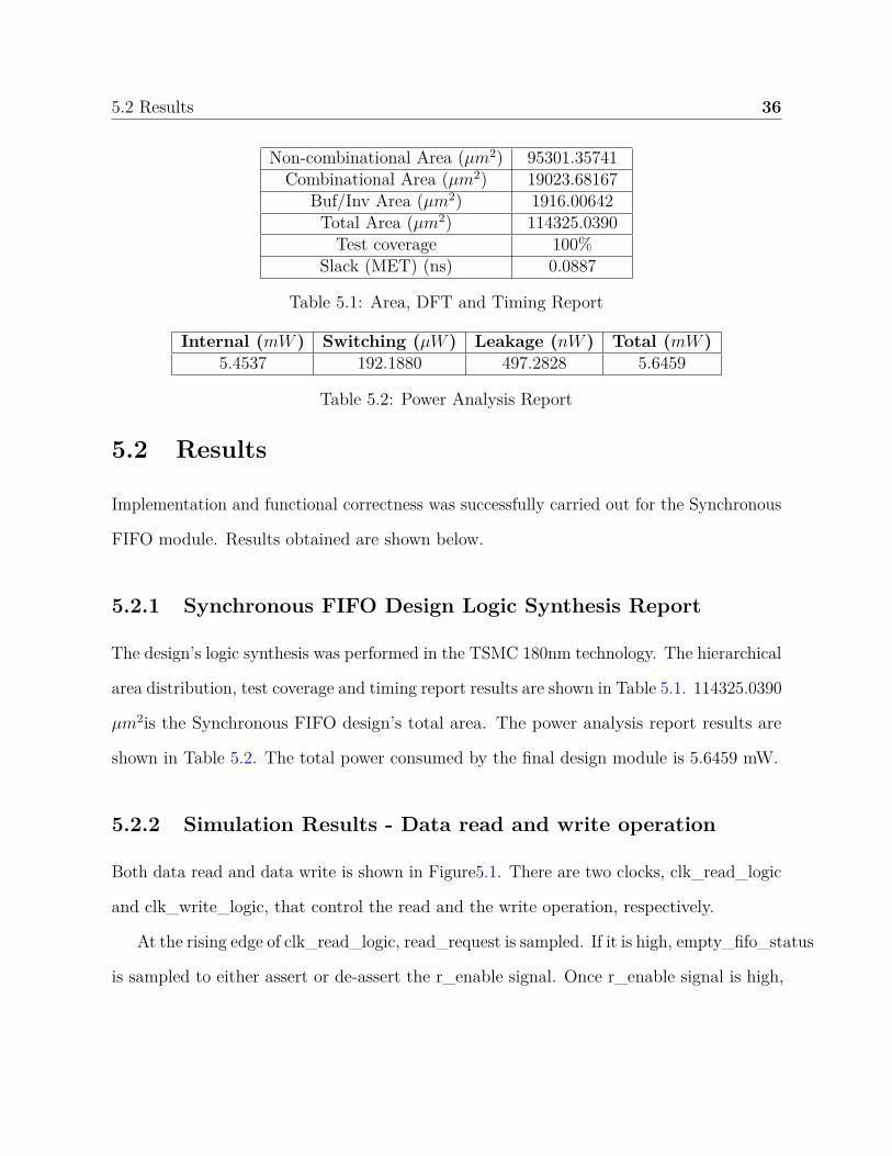
Non-combinational Area (µm2) 95301.35741Combinational Area (µm2) 19023.68167
Buf/Inv Area (µm2) 1916.00642Total Area (µm2) 114325.0390
Test coverage 100%Slack (MET) (ns) 0.0887
Table 5.1: Area, DFT and Timing Report
Internal (mW ) Switching (µW ) Leakage (nW ) Total (mW )5.4537 192.1880 497.2828 5.6459
Table 5.2: Power Analysis Report
5.2 Results
Implementation and functional correctness was successfully carried out for the Synchronous
FIFO module. Results obtained are shown below.
5.2.1 Synchronous FIFO Design Logic Synthesis Report
The design’s logic synthesis was performed in the TSMC 180nm technology. The hierarchical
area distribution, test coverage and timing report results are shown in Table 5.1. 114325.0390
µm2is the Synchronous FIFO design’s total area. The power analysis report results are
shown in Table 5.2. The total power consumed by the final design module is 5.6459 mW.
5.2.2 Simulation Results - Data read and write operation
Both data read and data write is shown in Figure5.1. There are two clocks, clk_read_logic
and clk_write_logic, that control the read and the write operation, respectively.
At the rising edge of clk_read_logic, read_request is sampled. If it is high, empty_fifo_status
is sampled to either assert or de-assert the r_enable signal. Once r_enable signal is high,

5.2 Results 37
Figure 5.1: Simulation Waveform
valid read operation takes place by reading the data from the memory array at the
read_pointer location.
At the rising edge of clk_write_logic, write request is sampled and if found high,
w_enable signal is either asserted or de-asserted based on the full_fifo_status signal. If
the memory array is full, full_fifo_status will be set. w_enable signal won’t be asserted,
when the memory array is full. Valid write operation takes place only when the w_enable
is high. It involves accessing the memory array location pointed by write_pointer to write
in the w_data.
5.2.3 Coverage
Code coverage and functional coverage[11] are essential in any verification plan. While code
coverage tells how much lines of code or block have been executed, functional coverage tries
to address other deficiencies in the DUT.
A covergroup is included in the sequencer part of the test bench that creates various
bins to cover all the possible values of w_data. In this case, coverage report would tell
if all the possible testcases are passed or not. For this project, the final coverage report
is checked using the Cadence Integrated Metrics Center (IMC) tool and both the code
coverage and the functional coverage where found to 100%.

Chapter 6
Conclusions
This chapter talks about conclusions and future work derived from this work.
6.1 Project Conclusions
This paper deals with the creation of a synchronous FIFO module and its verification using
UVM test bench environment. Three sub-modules of the synchronous FIFO design were
designed using Verilog HDL and integrated by instantiating all the three in the top-level
module. The test bench environment for this design was easily built by integrating all
the verification components which communicate with each other through ports and TLM
interfaces. It tries to verify the correct functionality of data write and data read with
proper flag triggers at the expected time. For achieving this, a reference model was written
mimicking the behavior of the Design under Test (DUT). Comparison with the DUT outputs
and the reference model outputs tells if the DUT functions correctly or not.
A covergroup was written in the sequencer part of the test bench to check if all the
possible cases of inputs are achieved and reports coverage judging the efficiency of the test

6.2 Future Work 39
bench environment.
6.2 Future Work
The current Synchronous FIFO design has a memory array of fixed depth (64) and fixed
data width (16 bits). Enhancements to the functionality of this design can be done by
including a logic that could bring about memory array’s width and depth expansion. This
depth expansion can be triggered, when new data has to be written during the memory
array’s full status. After adding such new features, the UVM test bench can be altered to
support the testing of new features as well.

References
[1] I. Miro Panades and A. Greiner. Bi-synchronous FIFO for synchronous circuit com-
munication well suited for network-on-chip in GALS architectures. In First In-
ternational Symposium on Networks-on-Chip (NOCS’07), pages 83–94, May 2007.
doi:10.1109/NOCS.2007.14.
[2] P. Coussy, A. Baganne, and E. Martin. A design methodology for integrating IP into
SOC systems. Proceedings of the IEEE 2002 Custom Integrated Circuits Conference
(Cat. No.02CH37285), pages 307–310, May 2002. doi:10.1109/CICC.2002.1012825.
[3] Allen E. Sjogren and Chris J. Myers. Interfacing synchronous and asynchronous modules
within a high-speed pipeline. IEEE Transactions on Very Large Scale Integration
(VLSI) Systems, 8(5):573–583, October 2000. doi:10.1109/92.894162.
[4] M. A. Khan and A. Q. Ansari. n-Bit multiple read and write FIFO memory model
for network-on-chip. In 2011 World Congress on Information and Communication
Technologies, pages 1326–1331, December 2011. doi:10.1109/WICT.2011.6141440.
[5] M. E. S. Elrabaa. A new FIFO design enabling fully-synchronous on-chip data
communication network. 2011 Saudi International Electronics, Communications and
Photonics Conference (SIECPC), pages 1–6, April 2011. doi:10.1109/SIECPC.2011.
5877006.

References 41
[6] D. Wyland. New features in synchronous FIFOs. In Proceedings of WESCON ’93,
pages 580–585, September 1993. doi:10.1109/WESCON.1993.488598.
[7] Geng Zhong, Jian Zhou, and Bei Xia. Parameter and UVM, making a layered testbench
powerful. In 2013 IEEE 10th International Conference on ASIC, pages 1–4, October
2013. doi:10.1109/ASICON.2013.6811929.
[8] K. Salah. A Unified UVM Architecture for Flash-Based Memory. In 2017 18th
International Workshop on Microprocessor and SOC Test and Verification (MTV),
pages 1–4. IEEE, December 2017. doi:10.1109/MTV.2017.10.
[9] Jiuling Tang. Design and FPGA implementation of a Viterbi decoder: A case study
using SystemVerilog and co-simulation. In 2009 IEEE International Symposium on
Signal Processing and Information Technology (ISSPIT), pages 1–6, December 2009.
doi:10.1109/ISSPIT.2009.5407512.
[10] G. Visalli. UVM-based verification of ECC module for flash memories. In 2017
European Conference on Circuit Theory and Design (ECCTD), pages 1–4, September
2017. doi:10.1109/ECCTD.2017.8093248.
[11] Accellera. Universal Verification Methodology 1.2 User’s Guide. page 190, 2015. URL:
http://www.accellera.org/downloads/standards/uvm.
[12] R. Sethulekshmi, S. Jazir, R. A. Rahiman, R. Karthik, S. Abdulla M, and S. Sree Swathy.
Verification of a RISC processor IP core using SystemVerilog. In 2016 International
Conference on Wireless Communications, Signal Processing and Networking (WiSP-
NET), pages 1490–1493, March 2016. doi:10.1109/WiSPNET.2016.7566385.
[13] Barada P. Biswal, Anurag Singh, and Balwinder Singh. Cache coherency controller veri-
fication IP using SystemVerilog Assertions (SVA) and Universal Verification Methodolo-

References 42
gies (UVM). Proceedings of 2017 11th International Conference on Intelligent Systems
and Control, ISCO 2017, pages 21–24, 2017. doi:10.1109/ISCO.2017.7855984.
[14] Zhili Zhou, Zheng Xie, Xin’An Wang, and Teng Wang. Development of verification
envioronment for SPI master interface using SystemVerilog. In 2012 IEEE 11th
International Conference on Signal Processing, volume 3, pages 2188–2192, October
2012. doi:10.1109/ICoSP.2012.6492015.
[15] H. Ke, D. Zhongliang, and S. Qiong. Verification of AMBA Bus Model Using SystemVer-
ilog. 2007 8th International Conference on Electronic Measurement and Instruments,
2:776–780, August 2007. doi:10.1109/ICEMI.2007.4350567.
[16] P. D. Mulani. SoC Level Verification Using System Verilog. In 2009 Second International
Conference on Emerging Trends in Engineering Technology, pages 378–380. IEEE,
December 2009. doi:10.1109/ICETET.2009.205.
[17] Prince Gurha and R. R. Khandelwal. SystemVerilog assertion based verification
of AMBA-AHB. Proceedings - 2016 International Conference on Micro-Electronics
and Telecommunication Engineering, ICMETE 2016, pages 641–645, 2017. doi:
10.1109/ICMETE.2016.67.
[18] C. Liang, G. Zhong, S. Huang, and B. Xia. UVM-AMS based sub-system verification
of wireless power receiver SoC. In 2014 12th IEEE International Conference on
Solid-State and Integrated Circuit Technology (ICSICT), pages 14–16, October 2014.
doi:10.1109/ICSICT.2014.7021458.
[19] Ivan Kastelan and Zoran Krajacevic. Synthesizable SystemVerilog assertions as a
methodology for SoC verification. ECBS-EERC 2009 - 1st Eastern European Re-

References 43
gional Conference on the Engineering of Computer-Based Systems: Setting New ECBS
Frontiers., pages 120–127, 2009. doi:10.1109/ECBS-EERC.2009.19.
[20] Hassan Sohofi and Zainalabedin Navabi. Assertion-Based Verification for System-Level
Designs. In Proceedings - International Symposium on Quality Electronic Design,
ISQED, March 2014. doi:10.1109/ISQED.2014.6783379.
[21] Moaz Mostafa, Mona Safar, M. Watheq El-Kharashi, and Mohamed Dessouky. Sys-
temVerilog assertion debugging: A visualization and pattern matching model. In
2015 IEEE Pacific Rim Conference on Communications, Computers and Signal
Processing (PACRIM), volume 2015-November, pages 385–390. IEEE, August 2015.
doi:10.1109/PACRIM.2015.7334867.
[22] Y. Tao. An introduction to assertion-based verification. In 2009 IEEE 8th International
Conference on ASIC, pages 1318–1323, October 2009. doi:10.1109/ASICON.2009.
5351246.
[23] IEEE Standard for SystemVerilog–Unified Hardware Design, Specification, and Ver-
ification Language. IEEE Std 1800-2017 (Revision of IEEE Std 1800-2012), pages
1–1315, February 2108. doi:10.1109/IEEESTD.2018.8299595.
[24] F. Neumann, M. Sathyamurthy, L. Kotynia, E. Hennig, and R. Sommer. UVM-
based verification of smart-sensor systems. In 2012 International Conference on
Synthesis, Modeling, Analysis and Simulation Methods and Applications to Circuit
Design (SMACD), number 2011, pages 21–24, September 2012. doi:10.1109/SMACD.
2012.6339407.
[25] Ashok B. Mehta. ASIC/SoC Functional Design Verification - A Comprehensive

References 44
Guide to Technologies and Methodologies. Springer International Publishing, 2018.
doi:10.1007/978-3-319-59418-7.

Appendix I
Source Code
I.1 Synchronous FIFO RTL
I.1.1 Write control logic
write_control.v1 //FIFO parameters2 `define FIFO_DEPTH 643 `define FIFO_MEM_ADDR_WIDTH 64 `define FIFO_HALFFULL 45
6 module write_control (7 reset,8 clk_write_logic,9 read_pointer,
10 write_request,11 w_enable,12 write_ack,13 write_pointer,14 full_fifo_status,15 halffull_fifo_status,16 wc_scan_in0,17 wc_scan_en,18 wc_test_mode,19 wc_scan_out020 );21
22 input reset;

I.1 Synchronous FIFO RTL I-2
23 input clk_write_logic;24 input reg [`FIFO_MEM_ADDR_WIDTH:0] read_pointer;25 input write_request;26 input reg wc_scan_in0, // test scan mode data input27 wc_scan_en, // test scan mode enable28 wc_test_mode; // test mode select29 output w_enable;30 output reg write_ack;31 output reg [`FIFO_MEM_ADDR_WIDTH:0] write_pointer;32 output full_fifo_status;33 output reg halffull_fifo_status;34 output wc_scan_out0; // test scan mode data35 output wire [`FIFO_MEM_ADDR_WIDTH-1:0] mem_addr_read;36
37 wire [`FIFO_MEM_ADDR_WIDTH-1:0] mem_addr_write;38
39 assign mem_addr_read = read_pointer [`FIFO_MEM_ADDR_WIDTH-1:0];40 assign mem_addr_write = write_pointer [`FIFO_MEM_ADDR_WIDTH-1:0];41 assign full_fifo_status = ((mem_addr_write == `FIFO_DEPTH - 1) &&
(read_pointer[`FIFO_MEM_ADDR_WIDTH] ^ write_pointer[`FIFO_MEM_ADDR_WIDTH]));↪→
42 assign w_enable = (write_request && (full_fifo_status==0))?1:0;43
44 always@(posedge clk_write_logic or posedge reset) begin45 if(reset) begin46 write_pointer <= 0;47 write_ack <= 0;48 end49 else begin50 halffull_fifo_status = ((`FIFO_DEPTH -
mem_addr_write)<=(`FIFO_HALFFULL))?1:0;↪→
51 if(w_enable) begin52 write_ack <= 1;53 write_pointer <= write_pointer + 1'b1;
↪→
54 end55 else56 write_ack <= 0;57 end58
59 end60
61 endmodule
I.1 Synchronous FIFO RTL I-3
I.1.2 Read control logic
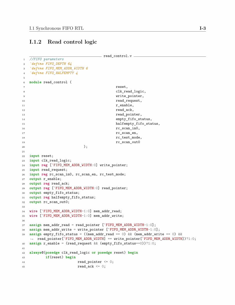
read_control.v1 //FIFO parameters2 `define FIFO_DEPTH 643 `define FIFO_MEM_ADDR_WIDTH 64 `define FIFO_HALFEMPTY 45
6 module read_control (7 reset,8 clk_read_logic,9 write_pointer,
10 read_request,11 r_enable,12 read_ack,13 read_pointer,14 empty_fifo_status,15 halfempty_fifo_status,16 rc_scan_in0,17 rc_scan_en,18 rc_test_mode,19 rc_scan_out020 );21
22 input reset;23 input clk_read_logic;24 input reg [`FIFO_MEM_ADDR_WIDTH:0] write_pointer;25 input read_request;26 input reg rc_scan_in0, rc_scan_en, rc_test_mode;27 output r_enable;28 output reg read_ack;29 output reg [`FIFO_MEM_ADDR_WIDTH:0] read_pointer;30 output empty_fifo_status;31 output reg halfempty_fifo_status;32 output rc_scan_out0;33
34 wire [`FIFO_MEM_ADDR_WIDTH-1:0] mem_addr_read;35 wire [`FIFO_MEM_ADDR_WIDTH-1:0] mem_addr_write;36
37 assign mem_addr_read = read_pointer [`FIFO_MEM_ADDR_WIDTH-1:0];38 assign mem_addr_write = write_pointer [`FIFO_MEM_ADDR_WIDTH-1:0];39 assign empty_fifo_status = ((mem_addr_read == 0) && (mem_addr_write == 0) &&
read_pointer[`FIFO_MEM_ADDR_WIDTH] == write_pointer[`FIFO_MEM_ADDR_WIDTH])?1:0;↪→
40 assign r_enable = (read_request && (empty_fifo_status==0))?1:0;41
42 always@(posedge clk_read_logic or posedge reset) begin43 if(reset) begin44 read_pointer <= 0;45 read_ack <= 0;

I.1 Synchronous FIFO RTL I-4
46 end47 else begin48 halfempty_fifo_status =
((mem_addr_read)<=(`FIFO_HALFEMPTY))?1:0;↪→
49 if(r_enable) begin50 read_ack <= 1;51 read_pointer <= read_pointer + 1'b1;52 end53 else54 read_ack <= 0;55 end56 end57
58 endmodule
I.1.3 Memory array
memory_array.v1 //FIFO parameters2 `define MEM_ADDR_WIDTH 63 `define MEM_DEPTH 644 `define MEM_DATA_WIDTH 165
6 module memory_array (7 input clk_write_logic,8 input clk_read_logic,9 input [`MEM_ADDR_WIDTH-1:0] w_addr,
10 input [`MEM_ADDR_WIDTH-1:0] r_addr,11 input w_enable,12 input r_enable,13 input reg [`MEM_DATA_WIDTH-1:0] w_data,14 input reg mem_scan_in0,15 input reg mem_scan_en,16 input reg mem_test_mode,17 output reg [`MEM_DATA_WIDTH-1:0] r_data,18 output mem_scan_out019 );20
21 reg [`MEM_DATA_WIDTH-1:0] memory [0:`MEM_DEPTH-1];22
23 always @(posedge clk_write_logic) begin24 if(w_enable)25 memory[w_addr] <= w_data;26 end27
28 always @(posedge clk_read_logic) begin

I.1 Synchronous FIFO RTL I-5
29 if(r_enable)30 r_data <= memory[r_addr];31 end32
33 endmodule
I.1.4 SFIFO
SFIFO.v1 `define FIFO_DEPTH 642 `define FIFO_MEM_ADDR_WIDTH 63 `define FIFO_MEM_DATA_WIDTH 164 `define FIFO_HALFEMPTY 45 `define FIFO_HALFFULL 46
7 module SFIFO (8 reset,9 clk_write_logic,
10 clk_read_logic,11 read_request,12 w_data,13 write_request,14 r_data,15 read_ack,16 w_enable,17 r_enable,18 empty_fifo_status,19 halfempty_fifo_status,20 full_fifo_status,21 halffull_fifo_status,22 write_ack,23 scan_in0,24 scan_en,25 test_mode,26 scan_out027 );28
29 input reset, // system reset30 clk_read_logic,31 clk_write_logic,32 read_request,33 write_request;34 input reg [`FIFO_MEM_DATA_WIDTH-1:0] w_data;35 input reg scan_in0, // test scan mode data input36 scan_en, // test scan mode enable37 test_mode; // test mode select

I.1 Synchronous FIFO RTL I-6
38
39 output reg [`FIFO_MEM_DATA_WIDTH-1:0] r_data;40 output w_enable, r_enable;41 output reg read_ack;42 output empty_fifo_status, full_fifo_status;43 output reg halfempty_fifo_status,44 halffull_fifo_status,45 write_ack;46 output scan_out0; // test scan mode data output47
48 reg [`FIFO_MEM_ADDR_WIDTH:0] read_pointer;49 reg [`FIFO_MEM_ADDR_WIDTH:0] write_pointer;50
51 wire [`FIFO_MEM_ADDR_WIDTH-1:0] w_addr;52 wire [`FIFO_MEM_ADDR_WIDTH-1:0] r_addr;53
54 assign w_addr = write_pointer [`FIFO_MEM_ADDR_WIDTH-1:0];55 assign r_addr = read_pointer [`FIFO_MEM_ADDR_WIDTH-1:0];56
57 read_control READ_CONTROL_MOD (58
59 .reset(reset),60 .clk_read_logic(clk_read_logic),61 .write_pointer(write_pointer),62 .read_request(read_request),63 .r_enable(r_enable),64 .read_ack(read_ack),65 .read_pointer(read_pointer),66 .empty_fifo_status(empty_fifo_status),67 .halfempty_fifo_status(halfempty_fifo_status),68 .rc_scan_in0(scan_in0),69 .rc_scan_en(scan_en),70 .rc_test_mode(test_mode),71 .rc_scan_out0(scan_out0)72
73 );74
75 write_control WRITE_CONTROL_MOD (76
77 .reset(reset),78 .clk_write_logic(clk_write_logic),79 .read_pointer(read_pointer),80 .write_request(write_request),81 .w_enable(w_enable),82 .write_ack(write_ack),83 .write_pointer(write_pointer),84 .full_fifo_status(full_fifo_status),85 .halffull_fifo_status(halffull_fifo_status),86 .wc_scan_in0(scan_in0),

I.2 UVM Testbench I-7
87 .wc_scan_en(scan_en),88 .wc_test_mode(test_mode),89 .wc_scan_out0(scan_out0)90
91 );92
93
94 memory_array MEM_ARRAY_MOD (95
96 .clk_write_logic(clk_write_logic),97 .clk_read_logic(clk_read_logic),98 .w_addr(w_addr),99 .r_addr(r_addr),
100 .w_enable(w_enable),101 .r_enable(r_enable),102 .w_data(w_data),103 .r_data(r_data),104 .mem_scan_in0(scan_in0),105 .mem_scan_en(scan_en),106 .mem_test_mode(test_mode),107 .mem_scan_out0(scan_out0)108
109
110 );111
112 endmodule
I.2 UVM Testbench
I.2.1 Interface
interface.sv1 `define ADDR_WIDTH 62 `define DATA_WIDTH 163
4 //-----------------------------Write control interface---------------------------------5 interface write_control_intf(input logic clk_write_logic, input logic reset);6 bit [`ADDR_WIDTH:0] read_pointer;7 logic write_request;8 logic w_enable;9 logic write_ack;
10 bit [`ADDR_WIDTH:0] write_pointer;11 logic full_fifo_status;12 logic halffull_fifo_status;

I.2 UVM Testbench I-8
13 logic scan_in0, scan_en, test_mode, scan_out0;14
15 clocking cb@(posedge clk_write_logic);16 output reset;17 output read_pointer;18 output write_request;19 output scan_in0, scan_en, test_mode;20 input w_enable;21 input write_ack;22 input write_pointer;23 input full_fifo_status;24 input halffull_fifo_status;25 input scan_out0;26 endclocking:cb27
28 modport WC(clocking cb, input clk_write_logic);29
30 endinterface:write_control_intf31 //-------------------------------------------------------------------------------------32
33 //----------------------------Read control interface-----------------------------------34 interface read_control_intf(input logic clk_read_logic, input logic reset);35 logic reset;36 bit [`ADDR_WIDTH:0] write_pointer;37 logic read_request;38 logic r_enable;39 logic read_ack;40 bit [`ADDR_WIDTH:0] read_pointer;41 logic empty_fifo_status;42 logic halfempty_fifo_status;43 logic scan_in0, scan_en, test_mode, scan_out0;44
45 clocking cb@(posedge clk_read_logic);46 output reset;47 output write_pointer;48 output read_request;49 output scan_in0, scan_en, test_mode;50 input r_enable;51 input read_ack;52 input read_pointer;53 input empty_fifo_status;54 input halfempty_fifo_status;55 input scan_out0;56 endclocking:cb57
58 modport RC(clocking cb, input clk_read_logic);59
60 endinterface:read_control_intf61 //-----------------------------------------------------------------------------------

I.2 UVM Testbench I-9
62
63 //---------------------------Memory array interface----------------------------------64 interface mem_array_intf(input logic clk_write_logic);65 logic clk_read_logic;66 bit [`ADDR_WIDTH-1:0] w_addr;67 bit [`ADDR_WIDTH-1:0] r_addr;68 logic w_enable;69 logic r_enable;70 bit [`DATA_WIDTH-1:0] w_data;71 bit [`DATA_WIDTH-1:0] r_data;72
73 clocking cb@(posedge clk_write_logic);74 output clk_read_logic;75 output w_addr;76 output r_addr;77 output w_enable;78 output r_enable;79 output w_data;80 input r_data;81 endclocking:cb82
83 modport MEM(clocking cb, input clk_write_logic);84
85 endinterface:mem_array_intf86
87 //----------------------------------------------------------------------------------
I.2.2 SFIFO_top_tb
SFIFO_top_tb.sv1 /* * Author: Vinoth Nagarajan2 * RIT, NY, USA3 * Module: SFIFO_top_tb */4
5 `include "interface.sv"6 `include "SFIFO_package.sv"7 `define write_logic_half_clock_period 1008 `define read_logic_half_clock_period 10009 //------------------------------------------------------------------------------------------
10
11 module test;12
13 //------------------------------------------------------------------------------------------↪→
14 import uvm_pkg::*;15 import SFIFO_package::*;

I.2 UVM Testbench I-10
16 //------------------------------------------------------------------------------------------17 bit clk_write_logic;18 bit clk_read_logic;19 bit reset;20 bit scan_en, scan_in0, test_mode;21 wire scan_out0;22 assign scan_out0 = 1'b0;23
24 initial begin25 scan_en = 1'b0;26 scan_in0 = 1'b0;27 test_mode = 1'b0;28 clk_write_logic = 1'b0;29 clk_read_logic = 1'b0;30 reset = 0;31 #25 reset = 1;32 #25 reset = 0;33 end34
35 always begin #`write_logic_half_clock_period clk_write_logic <= ~ clk_write_logic;36 #`read_logic_half_clock_period clk_read_logic <= ~ clk_read_logic;37 end38 //------------------------------------------------------------------------------------------39 //Interface instantiation40 write_control_intf w_ctrl(clk_write_logic, reset);41 read_control_intf r_ctrl(clk_read_logic, reset);42 mem_array_intf memory_intf(clk_write_logic);43 //------------------------------------------------------------------------------------------44 SFIFO top (45 .reset(w_ctrl.reset),46 .clk_write_logic(w_ctrl.clk_write_logic),47 .clk_read_logic(r_ctrl.clk_read_logic),48 .read_request(r_ctrl.read_request),49 .w_data(memory_intf.w_data),50 .write_request(w_ctrl.write_request),51 .r_data(memory_intf.r_data),52 .read_ack(r_ctrl.read_ack),53 .w_enable(w_ctrl.w_enable),54 .r_enable(r_ctrl.r_enable),55 .empty_fifo_status(r_ctrl.empty_fifo_status),56 .halfempty_fifo_status(r_ctrl.halfempty_fifo_status),57 .full_fifo_status(w_ctrl.full_fifo_status),58 .halffull_fifo_status(w_ctrl.halffull_fifo_status),59 .write_ack(w_ctrl.write_ack),60 .scan_in0(scan_in0),61 .scan_en(scan_en),62 .test_mode(test_mode),63 .scan_out0(scan_out0)64 );

I.2 UVM Testbench I-11
65 //------------------------------------------------------------------------------------------66
67 initial begin68 $set_coverage_db_name("SFIFO");69 $timeformat(-9,2,"ns", 16);70 `ifdef SDFSCAN71 $sdf_annotate("sdf/SFIFO_tsmc18_scan.sdf", test.top);72 `endif73 uvm_config_db#(virtual write_control_intf)::set(uvm_root::get(), "*",
"w_ctrl", w_ctrl);↪→
74 uvm_config_db#(virtual read_control_intf)::set(uvm_root::get(), "*", "r_ctrl",r_ctrl);↪→
75 uvm_config_db#(virtual mem_array_intf)::set(uvm_root::get(),"*", "memory_intf", memory_intf);↪→
76 run_test("test");77 end78
79 //------------------------------------------------------------------------------------------80 endmodule:test
I.2.3 SFIFO_test
SFIFO_test.sv1 /* * Author: Vinoth Nagarajan2 * RIT, NY, USA3 * Module: test */4
5 class test extends uvm_test;6 //------------------------------------------------------------------------------------------7 `uvm_component_utils (test)8 //------------------------------------------------------------------------------------------9 function new (string name="test", uvm_component parent=null);
10 super.new (name, parent);11 endfunction : new12 //------------------------------------------------------------------------------------------13 Environment t_env;14 SFIFO_sequence seq;15 SFIFO_sequence_items seq_items;16 //-----------------------------------------------------------------------------------------17 virtual function void build_phase(uvm_phase phase);18 super.build_phase(phase);19 `uvm_info(get_full_name(), "Build phase called in test", UVM_LOW)
↪→
20 t_env = Environment::type_id::create(.name("t_env"),.parent(this));↪→

I.2 UVM Testbench I-12
21 seq = SFIFO_sequence::type_id::create(.name("seq"), .parent(this));uvm_config_db#(uvm_object_wrapper)::set(this,"*",
"default_sequence", SFIFO_sequence::type_id::get());endfunction: build_phase
↪→
↪→
↪→
22 //-----------------------------------------------------------------------------------------23 virtual function void connect_phase(uvm_phase phase);24 super.connect_phase(phase);25 `uvm_info(get_full_name(), "Connect phase called in test", UVM_LOW)
↪→
26 endfunction: connect_phase27 //----------------------------------------------------------------------------------------28 virtual function void end_of_elaboration_phase(uvm_phase phase);
↪→
29 uvm_top.print_topology();30 endfunction: end_of_elaboration_phase
//-----------------------------------------------------------------------------------------↪→
31 function void start_of_simulation_phase(uvm_phase phase);32 super.start_of_simulation_phase (phase);33 endfunction: start_of_simulation_phase34 //----------------------------------------------------------------------------------------35 virtual task run_phase(uvm_phase phase);36 `uvm_info(get_full_name(), "in main phase", UVM_LOW)37 phase.raise_objection(.obj(this));38 seq.start(t_env.agent.sequencer);39 phase.drop_objection(.obj(this));40 endtask: run_phase41
42 //---------------------------------------------------------------------------------------43 endclass: test
I.2.4 SFIFO_env
SFIFO_env.sv1 /* * Author: Vinoth Nagarajan2 * RIT, NY, USA3 * Module: Environment */4
5 class Environment extends uvm_env;6 //--------------------------------------------------------------------------------------------
`uvm_component_utils(Environment)↪→
7 uvm_tlm_analysis_fifo #(SFIFO_sequence_items) to_refmod;8 //--------------------------------------------------------------------------------------------9 function new(string name="Environment", uvm_component parent=null);
↪→
10 super.new(name,parent);11 to_refmod = new("to_refmod", this);

I.2 UVM Testbench I-13
12 endfunction: new13 //-------------------------------------------------------------------------------------------14 SFIFO_agent agent;15 refmod_exec reference_mod;16 SFIFO_agent_out agent_out;17 SFIFO_scoreboard #(SFIFO_sequence_items_out) scoreboard;18 //-------------------------------------------------------------------------------------------19 virtual function void build_phase(uvm_phase phase);20 super.build_phase(phase);21 uvm_report_info(get_full_name(),"Build phase called in Environment",
UVM_LOW);↪→
22 agent = SFIFO_agent::type_id::create(.name("agent"), .parent(this));↪→
23 agent_out = SFIFO_agent_out::type_id::create(.name("agent_out"),.parent(this));↪→
24 reference_mod = refmod_exec::type_id::create(.name("reference_mod"),.parent(this));↪→
25 scoreboard = SFIFO_scoreboard#(SFIFO_sequence_items_out)::type_id::create(.name("scoreboard"),.parent(this));
uvm_report_info(get_full_name(),"Build phase inEnvironment ends", UVM_LOW);
↪→
↪→
↪→
↪→
26 endfunction: build_phase27 //-------------------------------------------------------------------------------------------28 virtual function void connect_phase(uvm_phase phase);29 super.connect_phase(phase);30 uvm_report_info(get_full_name(),"START of connect phase in
Environment",UVM_LOW);↪→
31 //Connect agent to FIFO32 agent.item_collected_port.connect(to_refmod.analysis_export);
↪→
33 //Connect FIFO to REFMOD34 reference_mod.in.connect(to_refmod.get_export);35 //Connect scoreboard36 reference_mod.out.connect(scoreboard.from_refmod);37 agent_out.item_collected_port.connect(scoreboard.from_dut);38 uvm_report_info(get_full_name(),"END of connect phase in
Environment",UVM_LOW);↪→
39 endfunction: connect_phase40 //--------------------------------------------------------------------------------------------41 virtual function void end_of_elaboration_phase(uvm_phase phase);42 super.end_of_elaboration_phase(phase);43 endfunction: end_of_elaboration_phase44 //--------------------------------------------------------------------------------------------
↪→
45 virtual function void report_phase(uvm_phase phase);46 super.report_phase(phase);47 `uvm_info(get_type_name(),48 $sformatf("Reporting matched %0d",

I.2 UVM Testbench I-14
49 scoreboard.m_matches), UVM_NONE)50 if (scoreboard.m_mismatches) begin51 `uvm_error(get_type_name(),52 $sformatf("Saw %0d mismatched
samples", scoreboard.m_mismatches))↪→
53 end54 endfunction: report_phase55 //-------------------------------------------------------------------------------------------56 endclass: Environment
I.2.5 SFIFO_agent
SFIFO_agent.sv1 /* * Author: Vinoth Nagarajan2 * RIT, NY, USA3 * Module: SFIFO_agent4 */5
6 class SFIFO_agent extends uvm_agent;7 //---------------------------------------------------------------------------------------------
`uvm_component_utils(SFIFO_agent)↪→
8 SFIFO_sequencer sequencer;9 SFIFO_driver driver;
10 SFIFO_monitor monitor;11 uvm_analysis_port#(SFIFO_sequence_items) item_collected_port;
//--------------------------------------------------------------------------------------------↪→
12 function new(string name = "SFIFO_agent", uvm_component parent);↪→
13 super.new(name, parent);14 item_collected_port = new("item_collected_port", this);15 endfunction: new16 //-------------------------------------------------------------------------------------------17 virtual function void build_phase(uvm_phase phase);18 super.build_phase(phase);19 `uvm_info(get_full_name(),"Build phase called in agent", UVM_LOW)
↪→
20 monitor = SFIFO_monitor::type_id::create("monitor", this);↪→
21 sequencer = SFIFO_sequencer::type_id::create(.name("sequencer"),.parent(this));↪→
22 driver = SFIFO_driver::type_id::create(.name("driver"), .parent(this));↪→
23 `uvm_info(get_full_name(),"Build phase ends in agent", UVM_LOW)↪→
24 endfunction: build_phase25 //------------------------------------------------------------------------------------------

I.2 UVM Testbench I-15
26 virtual function void connect_phase(uvm_phase phase);27 super.connect_phase(phase);28 `uvm_info(get_full_name(),"Connect phase called in agent",
UVM_LOW)monitor.item_collected_port.connect(item_collected_port);driver.seq_item_port.connect(sequencer.seq_item_export);
↪→
↪→
↪→
↪→
29 `uvm_info(get_full_name(),"Connect phase ends in agent", UVM_LOW)↪→
30 endfunction: connect_phase31 //------------------------------------------------------------------------------------------32 endclass: SFIFO_agent
I.2.6 SFIFO_agent_out
SFIFO_agent_out.sv1 /* * Author: Vinoth Nagarajan2 * RIT, NY, USA3 * Module: SFIFO_agent_out */4
5 class SFIFO_agent_out extends uvm_agent;//----------------------------------------------------------------------------------------↪→
6 `uvm_component_utils(SFIFO_agent_out)7 SFIFO_monitor_out mon_out;8 uvm_analysis_port #(SFIFO_sequence_items_out) item_collected_port;9 //----------------------------------------------------------------------------------------
10 function new(string name = "SFIFO_agent_out", uvm_component parent = null);11 super.new(name, parent);12 item_collected_port = new("item_collected_port", this);13 endfunction14 //----------------------------------------------------------------------------------------15 virtual function void build_phase(uvm_phase phase);16 super.build_phase(phase);17 mon_out = SFIFO_monitor_out::type_id::create("mon_out", this);18 endfunction19 //----------------------------------------------------------------------------------------20 virtual function void connect_phase(uvm_phase phase);21 super.connect_phase(phase);22 mon_out.item_collected_port.connect(item_collected_port);23 endfunction24 //----------------------------------------------------------------------------------------25 endclass: SFIFO_agent_out

I.2 UVM Testbench I-16
I.2.7 SFIFO_scoreboard
SFIFO_scoreboard.sv1 /* * Author: Vinoth Nagarajan2 * RIT, NY, USA3 * Module: SFIFO_scoreboard */4
5 class SFIFO_scoreboard #(type T = SFIFO_sequence_items_out) extends uvm_scoreboard;6 //----------------------------------------------------------------------------------------7 typedef SFIFO_scoreboard #(T) this_type;8 `uvm_component_param_utils(this_type)9 const static string type_name = "SFIFO_scoreboard #(T)";
10 uvm_put_imp #(T, this_type) from_refmod;11 uvm_analysis_imp #(T, this_type) from_dut;12 typedef uvm_built_in_converter #( T ) convert;13
14 int m_matches, m_mismatches;15 T exp;16 bit free;17 event compared, end_of_simulation;18 integer count;19 //-----------------------------------------------------------------------------------------20 function new(string name="SFIFO_scoreboard", uvm_component
parent=null);↪→
21 super.new(name, parent);22 from_refmod = new("from_refmod", this);23 from_dut = new("from_dut", this);24 m_matches = 0;25 count = 0;26 m_mismatches = 0;27 exp = new("exp");28 free = 0;29 endfunction30 //---------------------------------------------------------------------------------------31 virtual function string get_type_name();32 return type_name;33 endfunction34 //---------------------------------------------------------------------------------------35 task run_phase(uvm_phase phase);36 phase.raise_objection(this);37 @(end_of_simulation);38 $finish;39 phase.drop_objection(this);40 endtask41 //---------------------------------------------------------------------------------------42 virtual task put(T t);43 if(!free) @compared;44 exp.copy(t);45 free = 0;

I.2 UVM Testbench I-17
46 @compared;47 free = 1;48 endtask49 //---------------------------------------------------------------------------------------50 virtual function bit try_put(T t);51 if(free) begin52 exp.copy(t);53 free = 0;54 return 1;55 end56 else57 return 0;58 endfunction59 //---------------------------------------------------------------------------------------60 virtual function bit can_put();61 return free;62 endfunction63 //---------------------------------------------------------------------------------------64 virtual function void write(T rec);65 if (free)66 uvm_report_fatal("No expect transaction to compare
with", "");↪→
67 if (exp.compare(rec)) begin68 uvm_report_info("Comparator match", "");69 m_matches++;70 end71 else begin72 uvm_report_warning("Comparator Mismatch", "");73 m_mismatches++;74 end75
76 if(m_matches+m_mismatches > 1000) begin77 $display("---------------------------------------End-----------------------------------");
->end_of_simulation;↪→
78 end79 ->compared;80 endfunction81 //---------------------------------------------------------------------------------------82 endclass
I.2.8 SFIFO_refmod
SFIFO_refmod.sv1 /* * Author: Vinoth Nagarajan2 * RIT, NY, USA3 * Module: SFIFO_refmod */

I.2 UVM Testbench I-18
4
5 `define FIFO_DEPTH 646 `define FIFO_MEM_ADDR_WIDTH 67 `define FIFO_HALFFULL 48 `define FIFO_HALFEMPTY 49 //------------------------------------------------------------------------------------------
10 class SFIFO_refmod extends uvm_object;11 //------------------------------------------------------------------------------------------
↪→
12 SFIFO_sequence_items seq_in;13 `uvm_object_utils(SFIFO_refmod)14 bit [15:0] write_read_q[$];15 bit full,empty,almost_full,almost_empty;16 integer read_counter, write_counter;17 bit [15:0] rd;18 typedef bit [15:0] queue_of_int[$];19 virtual write_control_intf w_ctrl;20 virtual read_control_intf r_ctrl;21 virtual mem_array_intf memory_intf;22 //---------------------------------------------------------------------------------------23 function new (string name = "SFIFO_refmod");24 super.new(name);25 assert(uvm_config_db#(virtual write_control_intf)::get(uvm_root::get(),
"*", "w_ctrl", w_ctrl));assert(uvm_config_db#(virtual
read_control_intf)::get(uvm_root::get(), "*", "r_ctrl", r_ctrl));assert(uvm_config_db#(virtual
mem_array_intf)::get(uvm_root::get(), "*", "memory_intf",memory_intf)); seq_in =SFIFO_sequence_items::type_id::create("seq_in");
↪→
↪→
↪→
↪→
↪→
↪→
↪→
26 endfunction: new27 //-----------------------------------------------------------------------------------------
↪→
28 task refmod_reset;29 full = 0;30 empty = 0;31 almost_full = 0;32 almost_empty = 0;33 read_counter = 0;34 write_counter = 0;35 endtask: refmod_reset36 //----------------------------------------------------------------------------------------37 function int full_almostfull_status_check();38 if(write_counter == `FIFO_DEPTH - 1)39 return 1;40 else if((`FIFO_DEPTH - write_counter) <= `FIFO_HALFFULL)
↪→
41 return 2;42 else
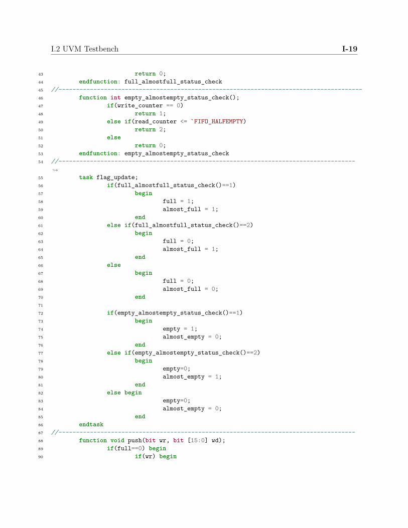
I.2 UVM Testbench I-19
43 return 0;44 endfunction: full_almostfull_status_check45 //---------------------------------------------------------------------------------------46 function int empty_almostempty_status_check();47 if(write_counter == 0)48 return 1;49 else if(read_counter <= `FIFO_HALFEMPTY)50 return 2;51 else52 return 0;53 endfunction: empty_almostempty_status_check54 //-------------------------------------------------------------------------------------
↪→
55 task flag_update;56 if(full_almostfull_status_check()==1)57 begin58 full = 1;59 almost_full = 1;60 end61 else if(full_almostfull_status_check()==2)62 begin63 full = 0;64 almost_full = 1;65 end66 else67 begin68 full = 0;69 almost_full = 0;70 end71
72 if(empty_almostempty_status_check()==1)73 begin74 empty = 1;75 almost_empty = 0;76 end77 else if(empty_almostempty_status_check()==2)78 begin79 empty=0;80 almost_empty = 1;81 end82 else begin83 empty=0;84 almost_empty = 0;85 end86 endtask87 //-------------------------------------------------------------------------------------88 function void push(bit wr, bit [15:0] wd);89 if(full==0) begin90 if(wr) begin

I.2 UVM Testbench I-20
91 write_read_q.push_front(wd);↪→
92 write_counter += 1;↪→
93 end94 end95 endfunction96 //------------------------------------------------------------------------------------97 function bit [15:0] pop(bit rr);98 if(empty==0) begin99 if(rr) begin
100 rd = write_read_q.pop_back();↪→
101 read_counter += 1;↪→
102 end103 return rd;104 end105 endfunction106 //-------------------------------------------------------------------------------------107 endclass: SFIFO_refmod108 //-------------------------------------------------------------------------------------109
110 //-------------------------------------------------------------------------------------------------111 class refmod_exec extends uvm_component;112 //-------------------------------------------------------------------------------------113 `uvm_component_utils(refmod_exec)114 SFIFO_sequence_items seq_in;115 SFIFO_sequence_items_out seq_out;116 virtual write_control_intf w_ctrl;117 virtual read_control_intf r_ctrl;118 virtual mem_array_intf memory_intf;119 SFIFO_refmod mod_ref;120 //------------------------------------------------------------------------------------121 uvm_get_port #(SFIFO_sequence_items) in;122 uvm_put_port #(SFIFO_sequence_items_out) out;123 //------------------------------------------------------------------------------------124 function new(string name = "refmod_exec", uvm_component parent);
↪→
125 super.new(name, parent);126 mod_ref = new();127 in = new("in", this);128 out = new("out", this);129 endfunction130 //------------------------------------------------------------------------------------131 virtual function void build_phase(uvm_phase phase);132 super.build_phase(phase);133 uvm_report_info(get_full_name(),"Build phase called in Reference model",
UVM_LOW);↪→
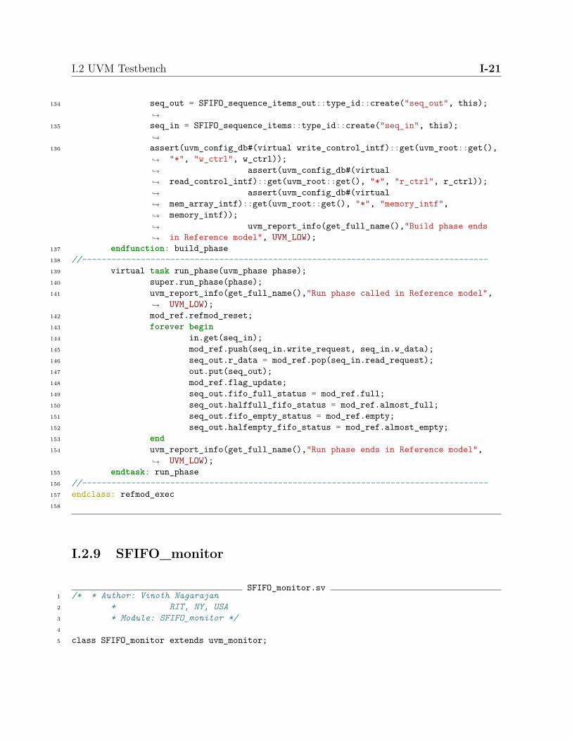
I.2 UVM Testbench I-21
134 seq_out = SFIFO_sequence_items_out::type_id::create("seq_out", this);↪→
135 seq_in = SFIFO_sequence_items::type_id::create("seq_in", this);↪→
136 assert(uvm_config_db#(virtual write_control_intf)::get(uvm_root::get(),"*", "w_ctrl", w_ctrl));
assert(uvm_config_db#(virtualread_control_intf)::get(uvm_root::get(), "*", "r_ctrl", r_ctrl));
assert(uvm_config_db#(virtualmem_array_intf)::get(uvm_root::get(), "*", "memory_intf",memory_intf));
uvm_report_info(get_full_name(),"Build phase endsin Reference model", UVM_LOW);
↪→
↪→
↪→
↪→
↪→
↪→
↪→
↪→
137 endfunction: build_phase138 //-----------------------------------------------------------------------------------139 virtual task run_phase(uvm_phase phase);140 super.run_phase(phase);141 uvm_report_info(get_full_name(),"Run phase called in Reference model",
UVM_LOW);↪→
142 mod_ref.refmod_reset;143 forever begin144 in.get(seq_in);145 mod_ref.push(seq_in.write_request, seq_in.w_data);146 seq_out.r_data = mod_ref.pop(seq_in.read_request);147 out.put(seq_out);148 mod_ref.flag_update;149 seq_out.fifo_full_status = mod_ref.full;150 seq_out.halffull_fifo_status = mod_ref.almost_full;151 seq_out.fifo_empty_status = mod_ref.empty;152 seq_out.halfempty_fifo_status = mod_ref.almost_empty;153 end154 uvm_report_info(get_full_name(),"Run phase ends in Reference model",
UVM_LOW);↪→
155 endtask: run_phase156 //-----------------------------------------------------------------------------------157 endclass: refmod_exec158
I.2.9 SFIFO_monitor
SFIFO_monitor.sv1 /* * Author: Vinoth Nagarajan2 * RIT, NY, USA3 * Module: SFIFO_monitor */4
5 class SFIFO_monitor extends uvm_monitor;

I.2 UVM Testbench I-22
6 //--------------------------------------------------------------------------------------------`uvm_component_utils(SFIFO_monitor)↪→
7 SFIFO_sequence_items seq_item;8 uvm_analysis_port #(SFIFO_sequence_items) item_collected_port;9 //--------------------------------------------------------------------------------------------
10 function new(string name="SFIFO_monitor", uvm_component parent=null);↪→
11 super.new(name, parent);12 item_collected_port = new ("item_collected_port", this);13 endfunction: new14 //------------------------------------------------------------------------------------------15 virtual write_control_intf w_ctrl;16 virtual read_control_intf r_ctrl;17 virtual mem_array_intf memory_intf;18 event begin_record, end_record;19 //-------------------------------------------------------------------------------------------20 virtual function void build_phase(uvm_phase phase);21 super.build_phase(phase);22 uvm_report_info(get_full_name(),"Build phase starts in monitor",
UVM_LOW);↪→
23 assert(uvm_config_db#(virtual write_control_intf)::get(this, "","w_ctrl", w_ctrl)); assert(uvm_config_db#(virtualread_control_intf)::get(this, "", "r_ctrl", r_ctrl));
assert(uvm_config_db#(virtualmem_array_intf)::get(this, "", "memory_intf", memory_intf));
↪→
↪→
↪→
↪→
↪→
24 seq_item = SFIFO_sequence_items::type_id::create("seq_item", this);↪→
25 uvm_report_info(get_full_name(),"Build phase ends in monitor", UVM_LOW);↪→
26 endfunction: build_phase27 //------------------------------------------------------------------------------------------28 virtual task run_phase(uvm_phase phase);29 super.run_phase(phase);30 uvm_report_info(get_full_name(),"Run phase starts in monitor", UVM_LOW);
↪→
31 collect_transactions(phase);32 uvm_report_info(get_full_name(),"Run phase ends in monitor", UVM_LOW);
↪→
33 endtask: run_phase34 //------------------------------------------------------------------------------------------35 task collect_transactions(uvm_phase phase);36 wait(w_ctrl.reset === 1);37 @(negedge w_ctrl.reset);38 forever begin39 -> begin_record;40 @(posedge w_ctrl.clk_write_logic) begin

I.2 UVM Testbench I-23
41 seq_item.write_request =w_ctrl.write_request;↪→
↪→
42 seq_item.w_data = memory_intf.w_data;↪→
43 end44 @(posedge r_ctrl.clk_read_logic)
↪→
45 seq_item.read_request =r_ctrl.read_request;↪→
46 item_collected_port.write(seq_item);47 -> end_record;48 end49 endtask: collect_transactions50 //----------------------------------------------------------------------------------------
↪→
51 task record_tr;52 forever begin53 @(begin_record);54 begin_tr(seq_item, "SFIFO_monitor");55 @(end_record);56 end_tr(seq_item);57 end58 endtask: record_tr59 //---------------------------------------------------------------------------------------60 endclass: SFIFO_monitor
I.2.10 SFIFO_monitor_out
SFIFO_monitor_out.sv1 /* * Author: Vinoth Nagarajan2 * RIT, NY, USA3 * Module: SFIFO_monitor_out */4
5 class SFIFO_monitor_out extends uvm_monitor;6 //-------------------------------------------------------------------------------------------
`uvm_component_utils(SFIFO_monitor_out)↪→
7 uvm_analysis_port #(SFIFO_sequence_items_out) item_collected_port;8 SFIFO_sequence_items_out seq_item;9 //-------------------------------------------------------------------------------------------
10 function new(string name="SFIFO_monitor_out", uvm_component parent=null);11 super.new(name, parent);12 item_collected_port = new ("item_collected_port", this);13 endfunction14 //------------------------------------------------------------------------------------------15 virtual write_control_intf w_ctrl;

I.2 UVM Testbench I-24
16 virtual read_control_intf r_ctrl;17 virtual mem_array_intf memory_intf;18 event begin_record, end_record;19 //------------------------------------------------------------------------------------------20 virtual function void build_phase(uvm_phase phase);21 super.build_phase(phase);22 uvm_report_info(get_full_name(),"Build phase starts in monitor_out",
UVM_LOW);↪→
23 assert(uvm_config_db#(virtual write_control_intf)::get(this, "","w_ctrl", w_ctrl));↪→
24 assert(uvm_config_db#(virtual read_control_intf)::get(this, "","r_ctrl", r_ctrl));↪→
25 assert(uvm_config_db#(virtual mem_array_intf)::get(this, "","memory_intf", memory_intf));↪→
26 seq_item = SFIFO_sequence_items_out::type_id::create("seq_item", this);↪→
27 uvm_report_info(get_full_name(),"Build phase ends in monitor_out",UVM_LOW);↪→
28 endfunction: build_phase29 //------------------------------------------------------------------------------------------30 virtual task run_phase(uvm_phase phase);31 super.run_phase(phase);32 uvm_report_info(get_full_name(),"Run phase starts in monitor_out",
UVM_LOW);↪→
33 collect_transactions(phase);34 uvm_report_info(get_full_name(),"Run phase ends in monitor_out",
UVM_LOW);↪→
35 endtask: run_phase36 //-----------------------------------------------------------------------------------------37 task collect_transactions(uvm_phase phase);38 wait(w_ctrl.reset === 1);39 @(negedge w_ctrl.reset);40 forever begin41 -> begin_record;42 @(posedge w_ctrl.clk_write_logic) begin
↪→
43 seq_item.fifo_full_status = w_ctrl.full_fifo_status;↪→
44 seq_item.halffull_fifo_status =w_ctrl.halffull_fifo_status;↪→
45 end46 @(posedge r_ctrl.clk_read_logic) begin
↪→
47 seq_item.halfempty_fifo_status =r_ctrl.halfempty_fifo_status;↪→
↪→
48 seq_item.fifo_empty_status = r_ctrl.empty_fifo_status;↪→

I.2 UVM Testbench I-25
49 if(r_ctrl.read_request)↪→
50 seq_item.r_data = memory_intf.r_data;↪→
51 end52 item_collected_port.write(seq_item);53 -> end_record;54 end55 endtask: collect_transactions56 //-----------------------------------------------------------------------------------------57 task record_tr;58 forever begin59 @(begin_record);60 begin_tr(seq_item, "SFIFO_monitor_out");61 @(end_record);62 end_tr(seq_item);63 end64 endtask: record_tr65 //---------------------------------------------------------------------------------------66 endclass: SFIFO_monitor_out
I.2.11 SFIFO_driver
SFIFO_driver.sv1 /* * Author: Vinoth Nagarajan2 * RIT, NY, USA3 * Module: SFIFO_driver */4
5 class SFIFO_driver extends uvm_driver #(SFIFO_sequence_items);6 //-------------------------------------------------------------------------------------------7 `uvm_component_utils(SFIFO_driver)8 //------------------------------------------------------------------------------------------9 //Constructor
10 function new (string name = "SFIFO_driver", uvm_component parent=null);↪→
11 super.new(name, parent);12 endfunction: new13 //------------------------------------------------------------------------------------------14 //Virtual interfaces declaration15 virtual write_control_intf w_ctrl;16 virtual read_control_intf r_ctrl;17 virtual mem_array_intf memory_intf;18 //------------------------------------------------------------------------------------------19 virtual function void build_phase(uvm_phase phase);20 `uvm_info(get_full_name(), "Build phase called in driver",
UVM_LOW)↪→

I.2 UVM Testbench I-26
21 super.build_phase(phase);22 assert(uvm_config_db#(virtual write_control_intf)::get(this, "",
"w_ctrl", w_ctrl));assert(uvm_config_db#(virtual
read_control_intf)::get(this, "", "r_ctrl", r_ctrl));assert(uvm_config_db#(virtual
mem_array_intf)::get(this, "", "memory_intf", memory_intf));`uvm_info(get_full_name(), "Build
phase ends in driver", UVM_LOW)
↪→
↪→
↪→
↪→
↪→
↪→
↪→
23 endfunction: build_phase24 //------------------------------------------------------------------------------------------25 //runs the necessary methods of the driver26 virtual task run_phase(uvm_phase phase);27 super.run_phase(phase);28 `uvm_info(get_full_name(), "Run phase called in driver",
UVM_LOW)↪→
29 fork30 reset_dut;31 drive(phase);32 join33 `uvm_info(get_full_name(), "Run phase called in driver",
UVM_LOW)↪→
34 endtask: run_phase35 //-----------------------------------------------------------------------------------------36 //Resets the DUT37 virtual protected task reset_dut;38 uvm_report_info(get_full_name(),"Start of reset_dut() method in driver",
UVM_LOW);↪→
39 wait(w_ctrl.reset==1);40 forever begin41 w_ctrl.write_ack <= '0;42 w_ctrl.write_pointer <= '0;43 w_ctrl.full_fifo_status <= '0;44 w_ctrl.halffull_fifo_status <= '0;45 w_ctrl.write_request <= '0;46 memory_intf.r_data <= 'x;47 memory_intf.w_data <= 'x;48 r_ctrl.read_ack <= '0;49 r_ctrl.read_request <= '0;50 r_ctrl.halfempty_fifo_status <= '0;51 r_ctrl.empty_fifo_status <= '0;52 r_ctrl.read_pointer <= '0;53 @(posedge w_ctrl.reset);54 end55 uvm_report_info(get_full_name(),"End of reset_dut() method in driver
",UVM_LOW);↪→
56 endtask : reset_dut57 //-------------------------------------------------------------------------------------------58 //Drives the stimulus to the DUT

I.2 UVM Testbench I-27
59 virtual protected task drive(uvm_phase phase);60 SFIFO_sequence_items stim;61 wait(w_ctrl.reset == 1);62 @(negedge w_ctrl.reset);63 @(posedge w_ctrl.clk_write_logic);64 forever begin65 seq_item_port.get_next_item(stim);66 uvm_report_info(get_full_name(),"Driving packet ...",UVM_LOW);67 @(posedge w_ctrl.clk_write_logic) begin
↪→
68 memory_intf.w_data = stim.w_data;↪→
69 w_ctrl.write_request = stim.write_request;↪→
70 end71 @(posedge r_ctrl.clk_read_logic)
↪→
72 r_ctrl.read_request=stim.read_request;↪→
73 @(posedge w_ctrl.clk_write_logic);74 seq_item_port.item_done();75 end76 endtask: drive77 //------------------------------------------------------------------------------------------78 endclass: SFIFO_driver79 //-----------------------------------------------------------------------------------------
I.2.12 SFIFO_sequencer
SFIFO_sequencer.sv1 /* * Author: Vinoth Nagarajan2 * RIT, NY, USA3 * Module: SFIFO_sequencer */4
5 `define FIFO_MEM_DATA_WIDTH 166 //---------------------------------------------------------------------------------------7 class SFIFO_sequence_items extends uvm_sequence_item;8 rand bit read_request;9 rand bit write_request;
10 rand bit [`FIFO_MEM_DATA_WIDTH-1:0] w_data;11 `uvm_object_utils_begin(SFIFO_sequence_items)12 `uvm_field_int(read_request, UVM_ALL_ON|UVM_DEFAULT)13 `uvm_field_int(write_request, UVM_ALL_ON|UVM_DEFAULT)14 `uvm_field_int(w_data, UVM_ALL_ON|UVM_DEFAULT)15 `uvm_object_utils_end16
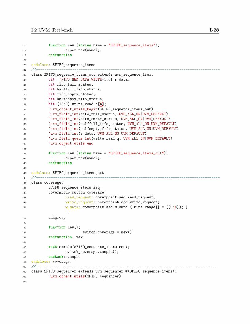
I.2 UVM Testbench I-28
17 function new (string name = "SFIFO_sequence_items");18 super.new(name);19 endfunction20
21 endclass: SFIFO_sequence_items22 //--------------------------------------------------------------------------------------23 class SFIFO_sequence_items_out extends uvm_sequence_item;24 bit [`FIFO_MEM_DATA_WIDTH-1:0] r_data;25 bit fifo_full_status;26 bit halffull_fifo_status;27 bit fifo_empty_status;28 bit halfempty_fifo_status;29 bit [15:0] write_read_q[$];30 `uvm_object_utils_begin(SFIFO_sequence_items_out)31 `uvm_field_int(fifo_full_status, UVM_ALL_ON|UVM_DEFAULT)32 `uvm_field_int(fifo_empty_status, UVM_ALL_ON|UVM_DEFAULT)33 `uvm_field_int(halffull_fifo_status, UVM_ALL_ON|UVM_DEFAULT)34 `uvm_field_int(halfempty_fifo_status, UVM_ALL_ON|UVM_DEFAULT)35 `uvm_field_int(r_data, UVM_ALL_ON|UVM_DEFAULT)36 `uvm_field_queue_int(write_read_q, UVM_ALL_ON|UVM_DEFAULT)37 `uvm_object_utils_end38
39 function new (string name = "SFIFO_sequence_items_out");40 super.new(name);41 endfunction42
43 endclass: SFIFO_sequence_items_out44 //--------------------------------------------------------------------------------------45 class coverage;46 SFIFO_sequence_items seq;47 covergroup switch_coverage;48 read_request: coverpoint seq.read_request;49 write_request: coverpoint seq.write_request;50 w_data: coverpoint seq.w_data { bins range[] = {[0:$]}; }
↪→
51 endgroup52
53 function new();54 switch_coverage = new();55 endfunction: new56
57 task sample(SFIFO_sequence_items seq);58 switch_coverage.sample();59 endtask: sample60 endclass: coverage61 //-------------------------------------------------------------------------------------62 class SFIFO_sequencer extends uvm_sequencer #(SFIFO_sequence_items);63 `uvm_object_utils(SFIFO_sequencer)64

I.2 UVM Testbench I-29
65 function new (string name="SFIFO_sequencer", uvm_component parent=null);↪→
66 super.new(name, parent);67 endfunction: new68
69 endclass: SFIFO_sequencer70 //-------------------------------------------------------------------------------------71 class SFIFO_sequence extends uvm_sequence #(SFIFO_sequence_items);72 `uvm_object_utils(SFIFO_sequence)73 coverage cov;74 SFIFO_sequence_items req;75
76 function new(string name="SFIFO_sequence");77 super.new(name);78 endfunction: new79
80 virtual task pre_body ();81 if (starting_phase != null)82 starting_phase.raise_objection (this);83 endtask84
85 virtual task body();86 forever begin87 repeat(5) begin88 req =
SFIFO_sequence_items::type_id::create("req");↪→
89 start_item(req);90 assert(req.randomize());
↪→
91 cov.sample(req);92 finish_item(req);93 end94 end95 endtask: body96
97 virtual task post_body();98 if (starting_phase != null)99 starting_phase.drop_objection (this);
100 endtask101
102 endclass: SFIFO_sequence103 //----------------------------------------------------------------------------------------------