Embed Size (px)
Citation preview
The Computer IS the Memory
Tom Coughlin, Coughlin Associates Jim Handy, Objective Analysis
© 2015 Coughlin Associates & Objective Analysis 1
CoughlinCoughlinData Storage Consulting
AssociatesAssociates
Outline
• The Shape of Things to Come • Getting Memory & Processing Closer • Spin-Based Memory and Processors • Conclusions
2 © 2015 Coughlin Associates & Objective Analysis

The Shape of Things to Come
© 2015 Coughlin Associates & Objective Analysis 3
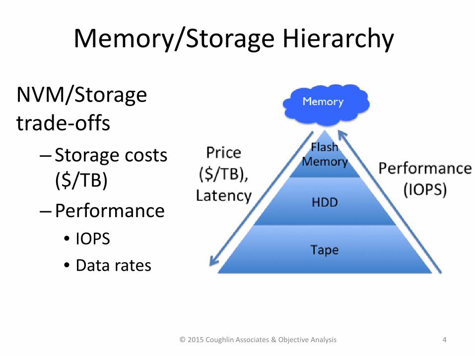
Memory/Storage Hierarchy
NVM/Storage trade-offs
– Storage costs ($/TB)
– Performance • IOPS • Data rates
4 © 2015 Coughlin Associates & Objective Analysis
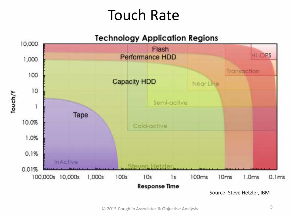
Touch Rate
5 © 2015 Coughlin Associates & Objective Analysis
Source: Steve Hetzler, IBM
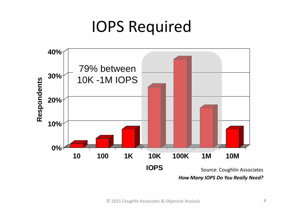
IOPS Required
0%
10%
20%
30%
40%
Res
pond
ents
10 100 1K 10K 100K 1M 10MIOPS
79% between 10K -1M IOPS
6 © 2015 Coughlin Associates & Objective Analysis
Source: Coughlin Associates How Many IOPS Do You Really Need?
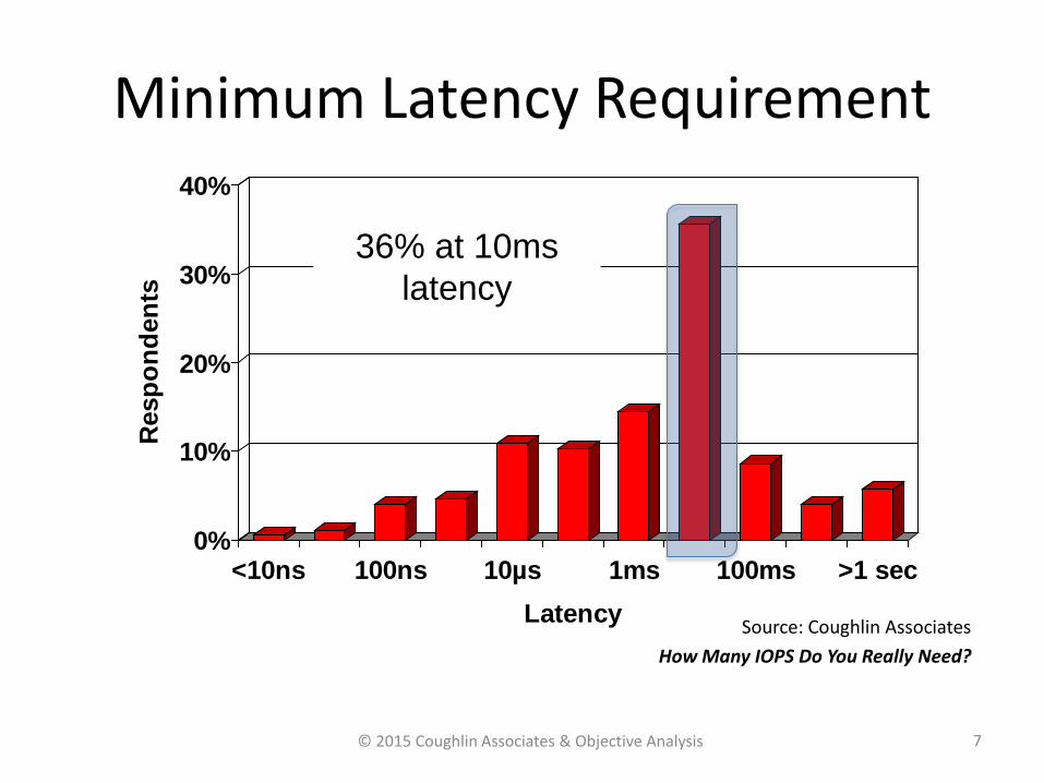
Minimum Latency Requirement
0%
10%
20%
30%
40%R
espo
nden
ts
<10ns 100ns 10µs 1ms 100ms >1 secLatency
36% at 10ms latency
7 © 2015 Coughlin Associates & Objective Analysis
Source: Coughlin Associates How Many IOPS Do You Really Need?
Persistent Memory Implications
• Retains data during a power loss – Instant recovery of state before power down
• Lower latencies than disk • Lower power than DRAM • Allows persistent states for Remote Direct
Memory Access (RDMA) • Supports “logic-in-memory architecture”
– Could lead to new distributed computer architectures
8 © 2015 Coughlin Associates & Objective Analysis
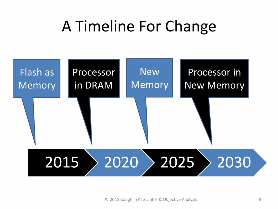
A Timeline For Change
2015 2020 2025 2030
Flash as Memory
New Memory
Processor in DRAM
Processor in New Memory
9 © 2015 Coughlin Associates & Objective Analysis
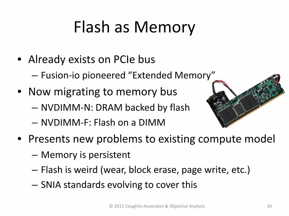
Flash as Memory
• Already exists on PCIe bus – Fusion-io pioneered “Extended Memory”
• Now migrating to memory bus – NVDIMM-N: DRAM backed by flash – NVDIMM-F: Flash on a DIMM
• Presents new problems to existing compute model – Memory is persistent – Flash is weird (wear, block erase, page write, etc.) – SNIA standards evolving to cover this
10 © 2015 Coughlin Associates & Objective Analysis
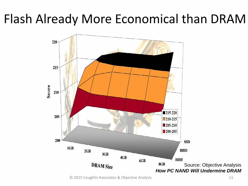
Flash Already More Economical than DRAM
Source: Objective Analysis How PC NAND Will Undermine DRAM
11 © 2015 Coughlin Associates & Objective Analysis
Getting Memory & Processing Closer
© 2015 Coughlin Associates & Objective Analysis 12
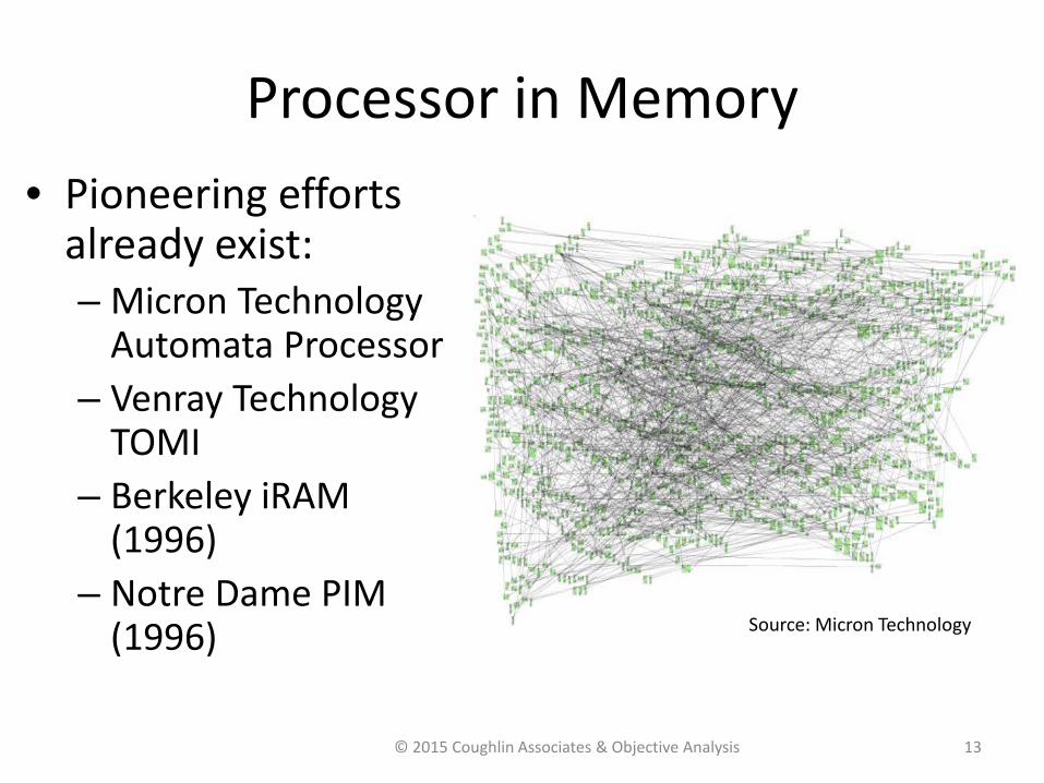
Processor in Memory • Pioneering efforts
already exist: – Micron Technology
Automata Processor – Venray Technology
TOMI – Berkeley iRAM
(1996) – Notre Dame PIM
(1996)
13 © 2015 Coughlin Associates & Objective Analysis
Source: Micron Technology
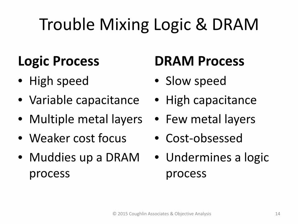
Trouble Mixing Logic & DRAM
Logic Process • High speed • Variable capacitance • Multiple metal layers • Weaker cost focus • Muddies up a DRAM
process
DRAM Process • Slow speed • High capacitance • Few metal layers • Cost-obsessed • Undermines a logic
process
14 © 2015 Coughlin Associates & Objective Analysis
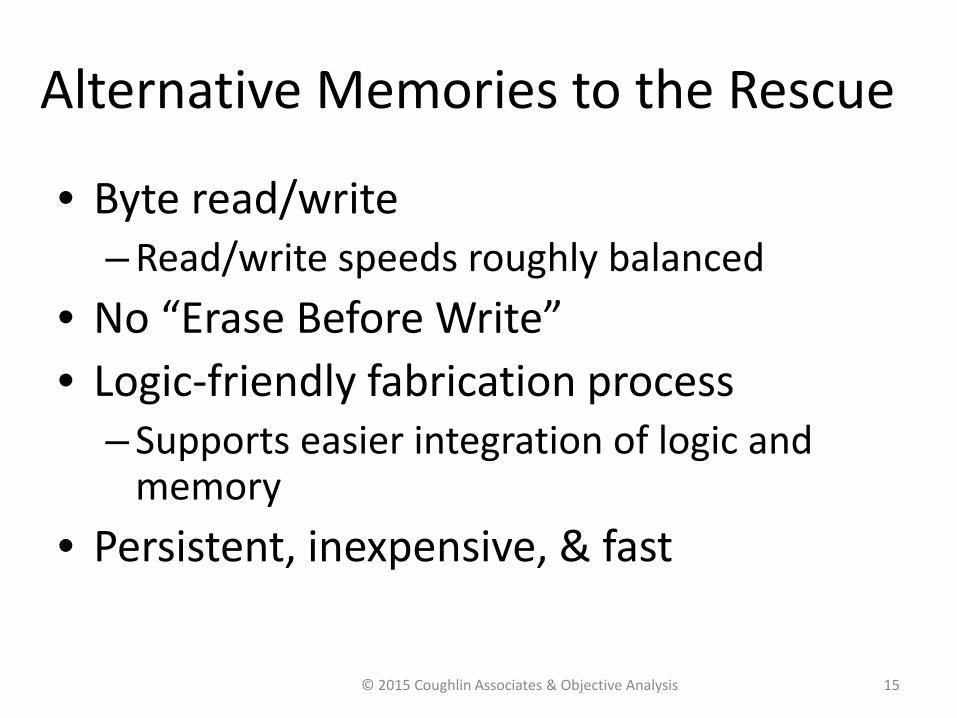
Alternative Memories to the Rescue
• Byte read/write – Read/write speeds roughly balanced
• No “Erase Before Write” • Logic-friendly fabrication process
– Supports easier integration of logic and memory
• Persistent, inexpensive, & fast
15 © 2015 Coughlin Associates & Objective Analysis
Yes, But Which New Memory Will Win?
• Many good alternatives: – STT MRAM – ReRAM – Memristor – Racetrack – PCM – FRAM
• Hard to know which will cross over DRAM & NAND pricing
16 © 2015 Coughlin Associates & Objective Analysis
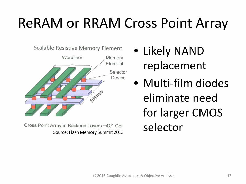
ReRAM or RRAM Cross Point Array
• Likely NAND replacement
• Multi-film diodes eliminate need for larger CMOS selector Source: Flash Memory Summit 2013
17 © 2015 Coughlin Associates & Objective Analysis
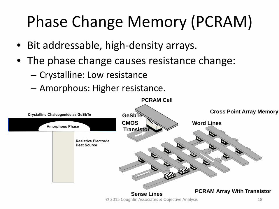
Phase Change Memory (PCRAM) • Bit addressable, high-density arrays. • The phase change causes resistance change:
– Crystalline: Low resistance – Amorphous: Higher resistance.
PCRAM Cell
PCRAM Array With Transistor
Word Lines
Sense Lines
Cross Point Array Memory
CMOS Transistor
GeSbTe
18 © 2015 Coughlin Associates & Objective Analysis
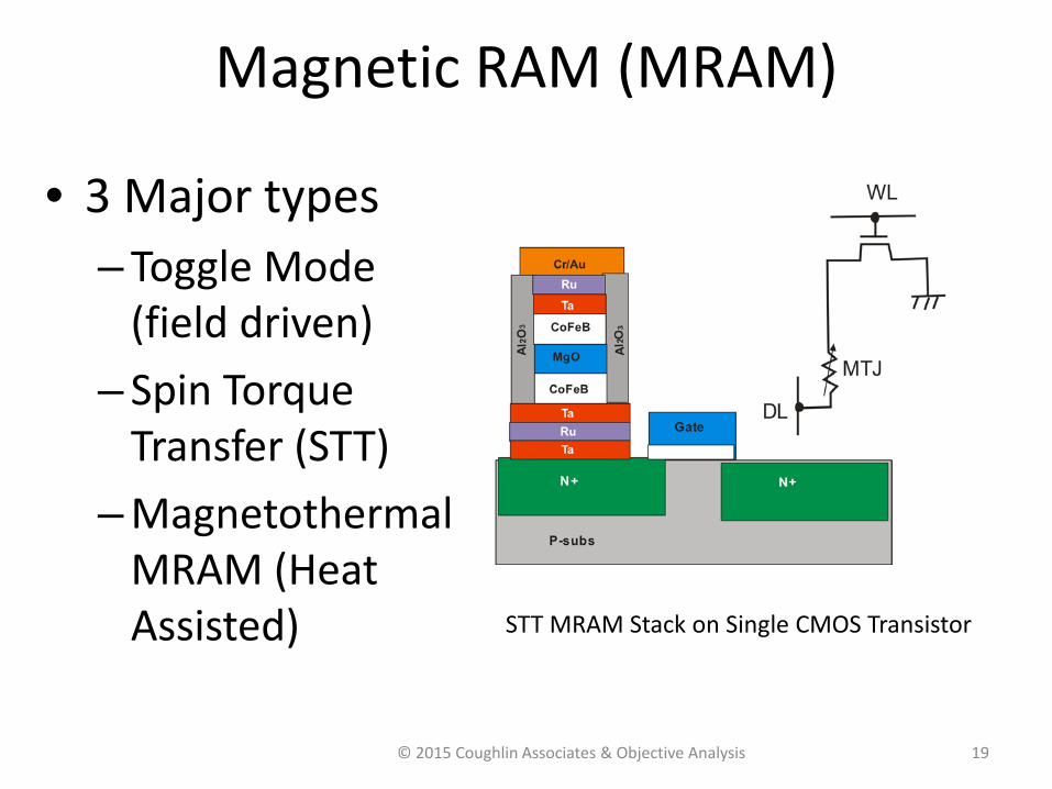
Magnetic RAM (MRAM)
• 3 Major types – Toggle Mode
(field driven) – Spin Torque
Transfer (STT) – Magnetothermal
MRAM (Heat Assisted) STT MRAM Stack on Single CMOS Transistor
19 © 2015 Coughlin Associates & Objective Analysis
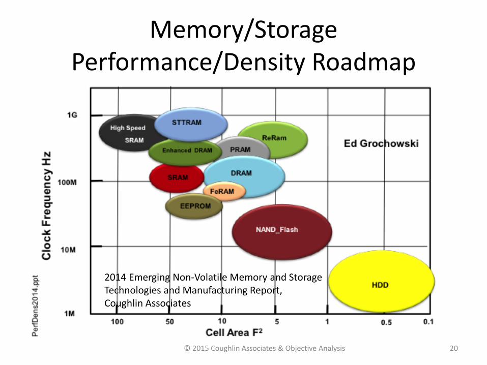
Memory/Storage Performance/Density Roadmap
20 © 2015 Coughlin Associates & Objective Analysis
2014 Emerging Non-Volatile Memory and Storage Technologies and Manufacturing Report, Coughlin Associates
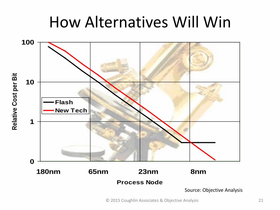
How Alternatives Will Win
0
1
10
100
180nm 65nm 23nm 8nmProcess Node
Rela
tive
Cost
per
Bit
FlashNew Tech
21 © 2015 Coughlin Associates & Objective Analysis
Source: Objective Analysis
The Impact of Moore’s Law • “Doubling transistors per chip every year or two”
– Put differently: “Making two chips into one every year or two”
• Using the 18-month rule of thumb – 2015 single-socket server with 96GB of RAM & an SSD
• 200-300 chips – 2030 – 15 years later
• About 1/5th to 1/3rd of one chip • Today’s 10,000-server data center could fit in 10
server slots! – Computing structures will adapt to this evolution
• Will Moore’s Law stop? Stay tuned!
22 © 2015 Coughlin Associates & Objective Analysis
Summary
• First step: Persistent Memory • Second Step: Processor in Memory • Third Step: Processor in Persistent Memory • Finally: Data Center in a Rack
Architectures and code will have to adapt!
23 © 2015 Coughlin Associates & Objective Analysis
24
Spin-Based Memory and
Processors
© 2015 Coughlin Associates & Objective Analysis
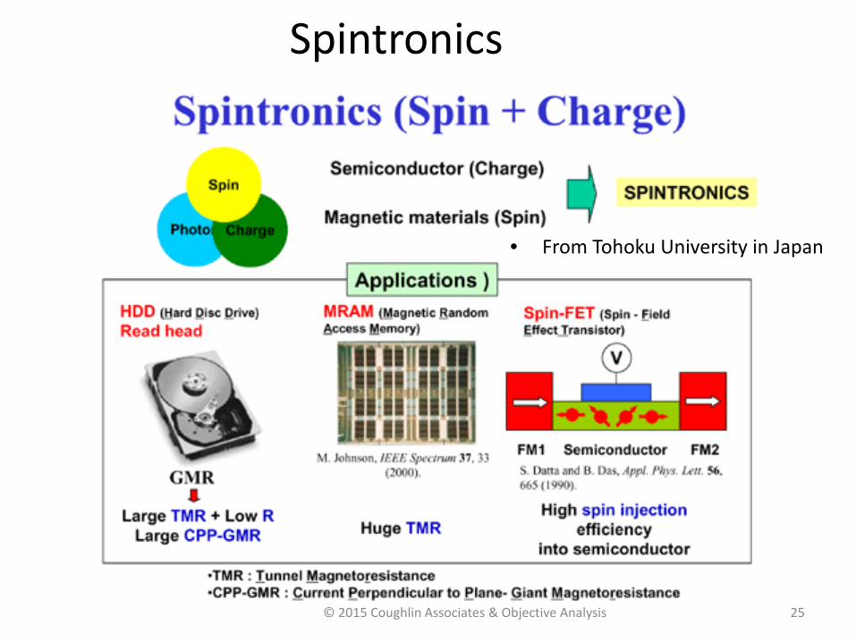
Spintronics
• From Tohoku University in Japan
25 © 2015 Coughlin Associates & Objective Analysis
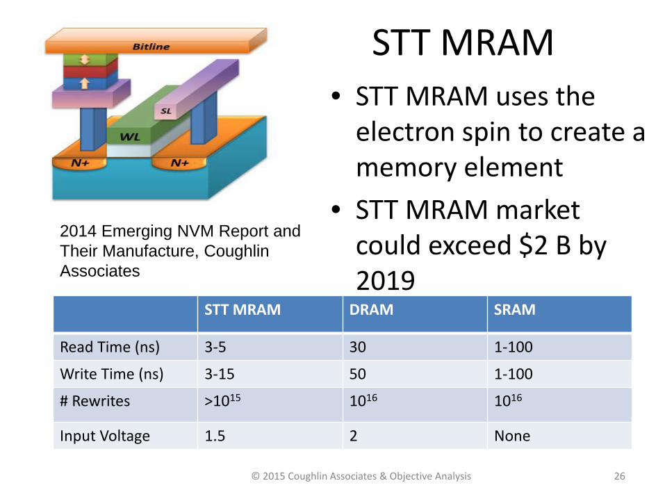
STT MRAM • STT MRAM uses the
electron spin to create a memory element
• STT MRAM market could exceed $2 B by 2019 STT MRAM DRAM SRAM
Read Time (ns) 3-5 30 1-100
Write Time (ns) 3-15 50 1-100
# Rewrites >1015 1016 1016
Input Voltage 1.5 2 None
26 © 2015 Coughlin Associates & Objective Analysis
2014 Emerging NVM Report and Their Manufacture, Coughlin Associates
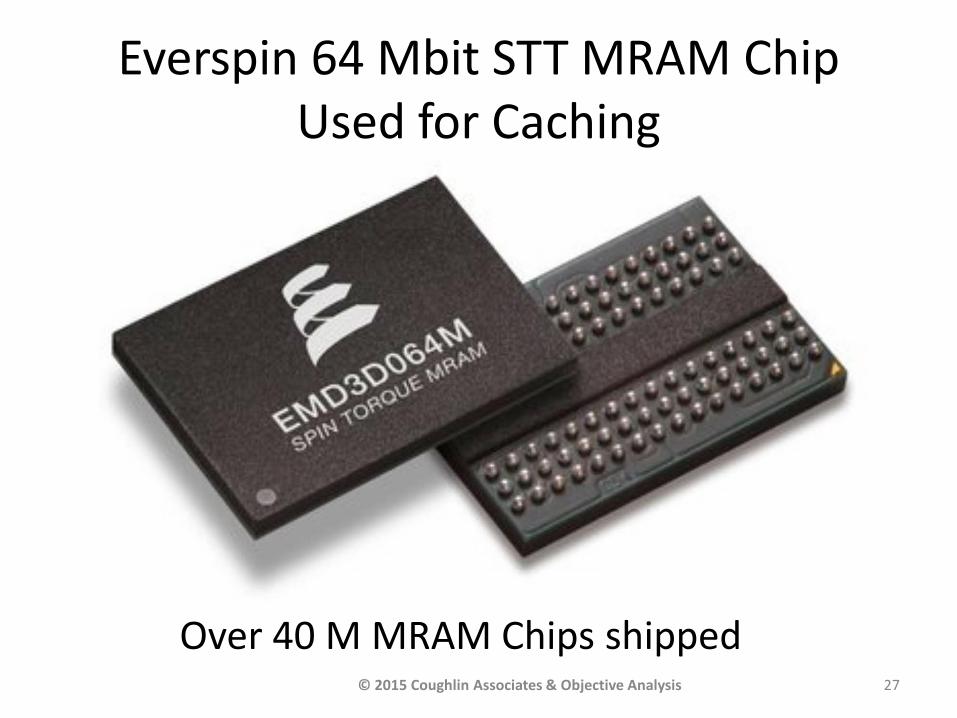
Everspin 64 Mbit STT MRAM Chip Used for Caching
27
Over 40 M MRAM Chips shipped © 2015 Coughlin Associates & Objective Analysis
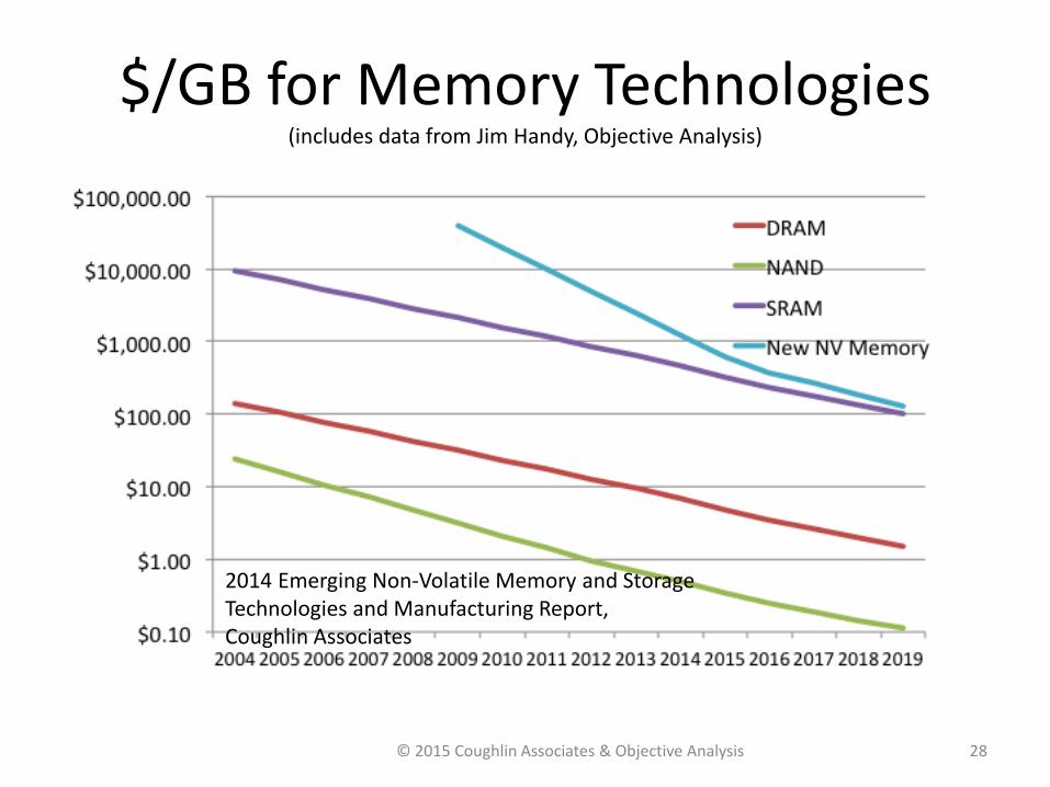
$/GB for Memory Technologies (includes data from Jim Handy, Objective Analysis)
28 © 2015 Coughlin Associates & Objective Analysis
2014 Emerging Non-Volatile Memory and Storage Technologies and Manufacturing Report, Coughlin Associates
What if Spin Transfer Replaced Charge Transfer (Current)?
• Spin transfer would not generate the heat that electrical currents generate
• Build powerful devices in small spaces
• Spin could be used for both processing and memory/storage
© 2015 Coughlin Associates & Objective Analysis 29
Conclusions
• The storage/memory landscape has more options than ever
• Non-volatile memories will replace volatile memories
• NVM and processors want to come together • Spin-based electronics are one example of a
technology that could put memory and processing in one device
© 2015 Coughlin Associates & Objective Analysis 30

© 2015 Coughlin Associates & Objective Analysis
Thanks
31