Embed Size (px)
Citation preview
MNRAS 000, 1–12 (2018) Preprint 16 November 2018 Compiled using MNRAS LATEX style file v3.0
The C-Band All-Sky Survey (C-BASS): Digital backend for thenorthern survey
M. A. Stevenson,1 T. J. Pearson,1? Michael E. Jones,2 C. J. Copley,2,3 C. Dickinson,4
J. J. John,2 O. G. King,1,2 S. J. C. Muchovej,1 and Angela C. Taylor21California Institute of Technology, Pasadena, CA 91125, USA2Sub-department of Astrophysics, University of Oxford, Denys Wilkinson Building, Keble Road, Oxford OX1 3RH, UK3Department of Physics and Electronics, Rhodes University, Drostdy Road, Grahamstown, 6139, South Africa4Jodrell Bank Centre for Astrophysics, School of Physics and Astronomy, The University of Manchester, Manchester, M13 9PL, UK
Accepted XXX. Received YYY; in original form ZZZ
ABSTRACTThe C-Band All-Sky Survey (C-BASS) is an all-sky full-polarization survey at a frequency of5 GHz, designed to provide data complementary to the all-sky surveys of WMAP and Planckand future CMB B-mode polarization imaging surveys. We describe the design and perfor-mance of the digital backend used for the northern part of the survey. In particular we describethe features that efficiently implement the demodulation and filtering required to suppresscontaminating signals in the time-ordered data, and the capability for real-time correction ofdetector non-linearity and receiver balance.
Key words: instrumentation: polarimeters – methods: data analysis – radio continuum: gen-eral
1 INTRODUCTION
The C-Band All-Sky Survey (C-BASS) is an all-sky full-polarization survey at a frequency of 5 GHz, designed to providedata complementary to the all-sky surveys of WMAP and Planckand future cosmic microwave background imaging surveys (Joneset al. 2018). It uses two single-dish radio telescopes, one in thenorthern hemisphere at the Owens Valley Radio Observatory, Cal-ifornia, and one in the southern hemisphere at the South AfricanRadio Astronomy Observatory site at Klerefontein. Although thetelescopes have different optics they have matched beams withFWHM 45 arcmin. Both telescopes are equipped with similar dual-polarization receivers that combine a continuous-comparison ra-diometer for measuring the Stokes parameter combinations I +Vand I−V with a correlation polarimeter for measuring Stokes Qand U by cross-correlation of the two circularly polarized signals.However, the two receivers differ in the implementation of the ra-diometer and polarimeter.
The northern receiver (King et al. 2014) uses analogue elec-tronics to process the 4.5 – 5.5 GHz radio frequency (RF) signalsin a single frequency channel, forming linear combinations of theorthogonal polarization voltages and reference signals using pas-sive microwave circuits, and ultimately producing analogue outputswhose powers are detected with Schottky diodes. The newer south-ern receiver (C. Copley et al., in preparation), in contrast, samples
? E-mail [email protected]
the voltages using high-speed digitizers, and all the subsequent sig-nal combination, power detection and integration are done usingdigital signal processing.
In this paper we present the design of the digital backendfor the northern receiver, which was operated between 2009 and2015. This system provided the sampling, data acquisition andread-out, as well as the phase-switching modulation scheme thatwas essential for the suppression of systematic effects in the re-ceiver. Section 2 summarizes the design of the northern receiverand the requirements it places on the backend. Section 3 describesthe backend hardware, and Section 4 describes the custom field-programmable gate array (FPGA) firmware developed to carryout the demodulation and integration and pass the data to a data-acquisition computer. We emphasize the novel filtering and timingalgorithms needed to carry out the processing in the FPGA envi-ronment. Section 5 presents the conclusions.
2 CONTEXT AND REQUIREMENTS
2.1 Receiver architecture
The C-BASS North receiver is a continuous-comparison radiome-ter combined with a correlation polarimeter (Jones et al. 2018;King et al. 2014). The radiometer architecture is similar to thoseof WMAP (Jarosik et al. 2003) and the Planck Low-Frequency In-strument (Seiffert et al. 2002). The receiver consists of a cryogenicsection containing the cold radio-frequency (RF) components, a
c© 2018 The Authors
arX
iv:1
811.
0612
4v1
[as
tro-
ph.I
M]
15
Nov
201
8
2 M. A. Stevenson et al.
warm receiver section of analogue RF components which imple-ments the radiometer and polarimeter, and a digital backend whichis the subject of this paper. The system estimates the Stokes param-eters I,Q,U,V from the complex voltages representing right andleft circular polarization EL and ER using (e.g., Hamaker & Breg-man 1996; Trippe 2014)
I = 〈ERE∗R〉+ 〈ELE∗L〉 (1)
Q = 〈ERE∗L〉+ 〈ELE∗R〉 (2)
U =−i[〈ERE∗L〉−〈ELE∗R〉] (3)
V = 〈ERE∗R〉−〈ELE∗L〉 . (4)
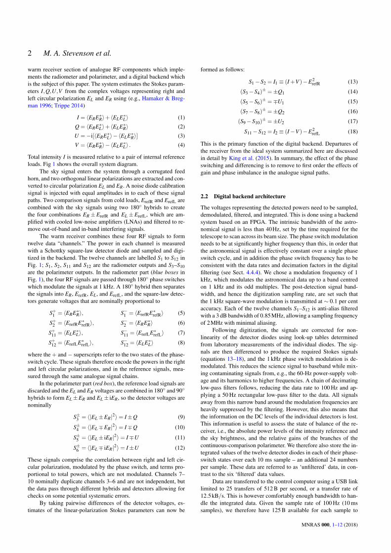
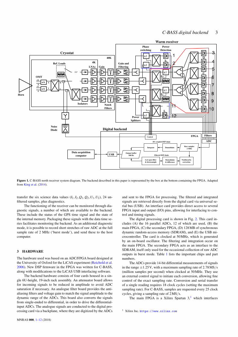
Total intensity I is measured relative to a pair of internal referenceloads. Fig 1 shows the overall system diagram.
The sky signal enters the system through a corrugated feedhorn, and two orthogonal linear polarizations are extracted and con-verted to circular polarization EL and ER. A noise diode calibrationsignal is injected with equal amplitudes in to each of these signalpaths. Two comparison signals from cold loads, ErefR and ErefL arecombined with the sky signals using two 180◦ hybrids to createthe four combinations ER ±ErefR and EL ±ErefL, which are am-plified with cooled low-noise amplifiers (LNAs) and filtered to re-move out-of-band and in-band interfering signals.
The warm receiver combines these four RF signals to formtwelve data “channels.” The power in each channel is measuredwith a Schottky square-law detector diode and sampled and digi-tized in the backend. The twelve channels are labelled S1 to S12 inFig. 1; S1, S2, S11 and S12 are the radiometer outputs and S3–S10are the polarimeter outputs. In the radiometer part (blue boxes inFig. 1), the four RF signals are passed through 180◦ phase switcheswhich modulate the signals at 1 kHz. A 180◦ hybrid then separatesthe signals into ER, ErefR, EL, and ErefL, and the square-law detec-tors generate voltages that are nominally proportional to
S+1 = 〈ERE∗R〉, S−1 = 〈ErefRE∗refR〉 (5)
S+2 = 〈ErefRE∗refR〉, S−2 = 〈ERE∗R〉 (6)
S+11 = 〈ELE∗L〉, S−11 = 〈ErefLE∗refL〉 (7)
S+12 = 〈ErefLE∗refL〉, S−12 = 〈ELE∗L〉 (8)
where the + and− superscripts refer to the two states of the phase-switch cycle. These signals therefore encode the powers in the rightand left circular polarizations, and in the reference signals, mea-sured through the same analogue signal chains.
In the polarimeter part (red box), the reference load signals arediscarded and the EL and ER voltages are combined in 180◦ and 90◦
hybrids to form EL±ER and EL± iER, so the detector voltages arenominally
S±3 = 〈|EL±ER|2〉= I±Q (9)
S±4 = 〈|EL∓ER|2〉= I∓Q (10)
S±5 = 〈|EL± iER|2〉= I∓U (11)
S±6 = 〈|EL∓ iER|2〉= I±U (12)
These signals comprise the correlation between right and left cir-cular polarization, modulated by the phase switch, and terms pro-portional to total powers, which are not modulated. Channels 7–10 nominally duplicate channels 3–6 and are not independent, butthe data pass through different hybrids and detectors allowing forchecks on some potential systematic errors.
By taking pairwise differences of the detector voltages, es-timates of the linear-polarization Stokes parameters can now be
formed as follows:
S1−S2 = I1 ≡ (I +V )−E2refR (13)
(S3−S4)± =±Q1 (14)
(S5−S6)± =∓U1 (15)
(S7−S8)± =±Q2 (16)
(S9−S10)± =±U2 (17)
S11−S12 = I2 ≡ (I−V )−E2refL (18)
This is the primary function of the digital backend. Departures ofthe receiver from the ideal system summarized here are discussedin detail by King et al. (2015). In summary, the effect of the phaseswitching and differencing is to remove to first order the effects ofgain and phase imbalance in the analogue signal paths.
2.2 Digital backend architecture
The voltages representing the detected powers need to be sampled,demodulated, filtered, and integrated. This is done using a backendsystem based on an FPGA. The intrinsic bandwidth of the astro-nomical signal is less than 40Hz, set by the time required for thetelescope to scan across its beam size. The phase switch modulationneeds to be at significantly higher frequency than this, in order thatthe astronomical signal is effectively constant over a single phaseswitch cycle, and in addition the phase switch frequency has to beconsistent with the data rates and decimation factors in the digitalfiltering (see Sect. 4.4.4). We chose a modulation frequency of 1kHz, which modulates the astronomical data up to a band centredon 1 kHz and its odd multiples. The post-detection signal band-width, and hence the digitization sampling rate, are set such thatthe 1 kHz square-wave modulation is transmitted at ∼ 0.1 per centaccuracy. Each of the twelve channels S1–S12 is anti-alias filteredwith a 3 dB bandwidth of 0.85MHz, allowing a sampling frequencyof 2MHz with minimal aliasing.
Following digitization, the signals are corrected for non-linearity of the detector diodes using look-up tables determinedfrom laboratory measurements of the individual diodes. The sig-nals are then differenced to produce the required Stokes signals(equations 13–18), and the 1 kHz phase switch modulation is de-modulated. This reduces the science signal to baseband while mix-ing contaminating signals from, e.g., the 60-Hz power-supply volt-age and its harmonics to higher frequencies. A chain of decimatinglow-pass filters follows, reducing the data rate to 100 Hz and ap-plying a 50 Hz rectangular low-pass filter to the data. All signalsaway from this narrow band around the modulation frequencies areheavily suppressed by the filtering. However, this also means thatthe information on the DC levels of the individual detectors is lost.This information is useful to assess the state of balance of the re-ceiver, i.e., the absolute power levels of the intensity reference andthe sky brightness, and the relative gains of the branches of thecontinuous-comparison polarimeter. We therefore also store the in-tegrated values of the twelve detector diodes in each of their phase-switch states over each 10 ms sample – an additional 24 numbersper sample. These data are referred to as ‘unfiltered’ data, in con-trast to the six ‘filtered’ data values.
Data are transferred to the control computer using a USB linklimited to 25 transfers of 512 B per second, or a transfer rate of12.5kB/s. This is however comfortably enough bandwidth to han-dle the integrated data. Given the sample rate of 100 Hz (10 mssamples), we therefore have 125 B available for each sample to
MNRAS 000, 1–12 (2018)
C-BASS digital backend 3
±1
±1
±1
±1
180°
180°
180°
180°
±1
±1
90°
180°
180°
90°
OMT
180°
180°
Gain and Filtering
40K4K
L
R
Warm receiver
Ref. Loads
ADC
USB
Control Filters
Data acquisitioncomputer
Phaseswitching
PowerDetection
U
-U
Q
Q
IR
IL
NoiseDiode
Horn
Cryostat
GainLNAs
NotchFilters
+Y
+X
ER
PowerSplitters
EL
Isolators
-X
-Y
a-b
a-b
90°X
Y
Raw samples2 MHzDemodulateIntegrate
Nonlinearitycorrection
Demodulate& difference
Low-pass filter& downsample
Output buffer100 Hz
FPGA
Digital backend
DC-coupled DSP chain
Filtered DSP chain
1
2
11
12
3
45
6
7
89
10
Figure 1. C-BASS north receiver system diagram. The backend described in this paper is represented by the box at the bottom containing the FPGA. Adaptedfrom King et al. (2014).
transfer the six science data values (I1, I2,Q1,Q2,U1,U2), 24 un-filtered samples, plus diagnostics.
The functioning of the receiver can be monitored through dia-gnostic signals, a number of which are available to the backend.These include the status of the GPS time signal and the state ofthe internal memory. Packaging these signals with the data time se-ries facilitates monitoring the backend. As an additional diagnosticmode, it is possible to record short stretches of raw ADC at the fullsample rate of 2 MHz (‘burst mode’), and send these to the hostcomputer.
3 HARDWARE
The hardware used was based on an ADC/FPGA board designed atthe University of Oxford for the LiCAS experiment (Reichold et al.2006). New DSP firmware in the FPGA was written for C-BASS,along with modifications to the LiCAS USB interfacing software.
The backend hardware consists of four cards housed in a sin-gle 6U-height, 19-inch rack assembly. An attenuator board allowsfor incoming signals to be reduced in amplitude to avoid ADCsaturation if necessary. An analogue filter board provides the anti-aliasing filters and voltage gain to match the signal amplitude to thedynamic range of the ADCs. This board also converts the signalsfrom single-ended to differential, in order to drive the differential-input ADCs. The analogue signals are conducted to the digital pro-cessing card via a backplane, where they are digitized by the ADCs
and sent to the FPGA for processing. The filtered and integratedsignals are retrieved directly from the digital card via universal se-rial bus (USB). An interface card provides direct access to severalFPGA input and output (I/O) pins, allowing for interfacing to con-trol and timing signals.
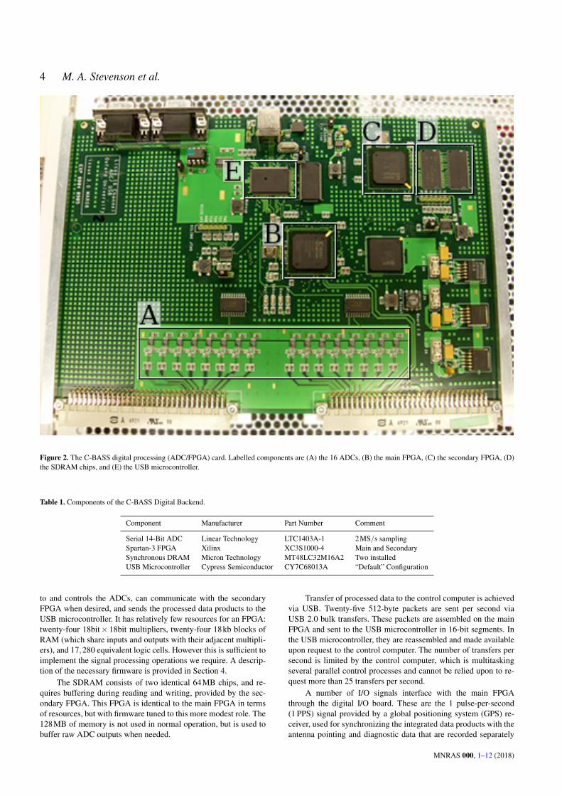
The digital processing card is shown in Fig. 2. This card in-cludes (A) the 16 parallel ADCs, 12 of which are used, (B) themain FPGA, (C) the secondary FPGA, (D) 128MB of synchronousdynamic random-access memory (SDRAM), and (E) the USB mi-crocontroller. The card is clocked at 50MHz, which is generatedby an on-board oscillator. The filtering and integration occur onthe main FPGA. The secondary FPGA acts as an interface to theSDRAM, itself only used for the occasional collection of raw ADCoutputs in burst mode. Table 1 lists the important chips and partnumbers.
The ADCs provide 14-bit differential measurements of signalsin the range±1.25V, with a maximum sampling rate of 2.78MS/s(million samples per second) when clocked at 50MHz. They usean external control signal to initiate each conversion, allowing finecontrol of the exact sampling rate. Conversion and serial transferof a single reading requires 18 clock cycles (setting the maximumsampling rate). For C-BASS, samples are requested every 25 clockcycles, giving a sampling rate of 2MS/s.
The main FPGA is a Xilinx Spartan 3,1 which interfaces
1 Xilinx Inc. https://www.xilinx.com
MNRAS 000, 1–12 (2018)
4 M. A. Stevenson et al.
Figure 2. The C-BASS digital processing (ADC/FPGA) card. Labelled components are (A) the 16 ADCs, (B) the main FPGA, (C) the secondary FPGA, (D)the SDRAM chips, and (E) the USB microcontroller.
Table 1. Components of the C-BASS Digital Backend.
Component Manufacturer Part Number Comment
Serial 14-Bit ADC Linear Technology LTC1403A-1 2MS/s samplingSpartan-3 FPGA Xilinx XC3S1000-4 Main and SecondarySynchronous DRAM Micron Technology MT48LC32M16A2 Two installedUSB Microcontroller Cypress Semiconductor CY7C68013A “Default” Configuration
to and controls the ADCs, can communicate with the secondaryFPGA when desired, and sends the processed data products to theUSB microcontroller. It has relatively few resources for an FPGA:twenty-four 18bit× 18bit multipliers, twenty-four 18kb blocks ofRAM (which share inputs and outputs with their adjacent multipli-ers), and 17,280 equivalent logic cells. However this is sufficient toimplement the signal processing operations we require. A descrip-tion of the necessary firmware is provided in Section 4.
The SDRAM consists of two identical 64MB chips, and re-quires buffering during reading and writing, provided by the sec-ondary FPGA. This FPGA is identical to the main FPGA in termsof resources, but with firmware tuned to this more modest role. The128MB of memory is not used in normal operation, but is used tobuffer raw ADC outputs when needed.
Transfer of processed data to the control computer is achievedvia USB. Twenty-five 512-byte packets are sent per second viaUSB 2.0 bulk transfers. These packets are assembled on the mainFPGA and sent to the USB microcontroller in 16-bit segments. Inthe USB microcontroller, they are reassembled and made availableupon request to the control computer. The number of transfers persecond is limited by the control computer, which is multitaskingseveral parallel control processes and cannot be relied upon to re-quest more than 25 transfers per second.
A number of I/O signals interface with the main FPGAthrough the digital I/O board. These are the 1 pulse-per-second(1 PPS) signal provided by a global positioning system (GPS) re-ceiver, used for synchronizing the integrated data products with theantenna pointing and diagnostic data that are recorded separately
MNRAS 000, 1–12 (2018)
C-BASS digital backend 5
by the control system; the six 180◦ phase switches in the analoguereceiver; and the on/off switch for the calibration noise diode.
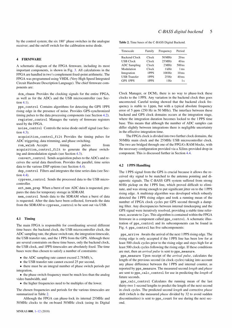
4 FIRMWARE
A schematic diagram of the FPGA firmware, including its mostimportant components, is shown in Fig. 3. All calculations in theFPGA are handled in two’s complement fixed-point arithmetic. TheFPGA was programmed using VHDL (Very High Speed IntegratedCircuit Hardware Description Language). The chief firmware com-ponents are:
dcm_cbass Provides the clocking signals for the entire FPGA,as well as for the ADCs and the USB microcontroller (see Sec-tion 4.1).pps_control Contains algorithms for detecting the GPS 1PPS
rising edge in the presence of noise. Provides GPS-synchronizedtiming pulses to the data processing components (see Section 4.2).register_control Manages the variety of firmware registers
used by the FPGA.noise_control Controls the noise diode on/off signal (see Sec-
tion 4.3).acquisition_control_filt Provides the timing pulses for
ADC triggering, data trimming, and phase switching.rom_walsh Accepts timing pulses fromacquisition_control_filt to generate the phase switch-ing and demodulation signals (see Section 4.3).convert_control Sends acquisition pulses to the ADCs and re-
ceives the serial data therefrom. Provides the parallel, time seriesdata to the various DSP options (see Section 4.4).dsp_control Filters and integrates the time series data (see Sec-
tion 4.4).cypress_control Sends the processed data to the USB micro-
controller.ext_mem_prep When a burst of raw ADC data is requested, pre-
pares the data for temporary storage in SDRAM.mem_control Sends data to the SDRAM when a burst of data
is requested. After the data have been collected, forwards the datafrom the SDRAM to cypress_control to be sent out via USB.
4.1 Timing
The main FPGA is responsible for coordinating several differenttime bases: the backend clock, the USB microcontroller clock, theADC sampling rate, the phase switch rate, the integration timescale,the USB transfer rate, and the 1 PPS from the GPS. Although thereare several constraints on these time bases, only the backend clock,the USB clock, and 1PPS timescales are absolutely fixed. The timebases were thus chosen to satisfy a number of constraints:
• the ADC sampling rate cannot exceed 2.78MS/s,• the USB transfer rate cannot exceed 25 per second,• there must be an integral number of phase switch periods per
integration,• the phase switch frequency must be much less than the analog
video bandwidth, and• the higher frequencies need to be multiples of the lower.
The chosen frequencies and periods for the various timescales aresummarized in Table 2.
Although the FPGA can phase-lock its internal 25MHz and50MHz clocks to the on-board 50MHz clock (using its Digital
Table 2. Time bases of the C-BASS Digital Backend.
Timescale Family Frequency Period
Backend Clock Clock 50MHz 20nsUSB Clock Clock 25MHz 40nsADC Sampling Clock 2MHz 500nsModulation Clock 1kHz 1msIntegration 1PPS 100Hz 10msUSB Transfer 1PPS 25Hz 40msGPS 1PPS 1PPS 1Hz 1s
Clock Manager, or DCM), there is no way to phase-lock theseclocks to the 1 PPS. Any variation in the backend clock thus goesuncorrected. Careful testing showed that the backend clock fre-quency is stable to 1ppm, but with a typical absolute frequencyerror of 5 ppm (250 Hz in 50 MHz). The interface between thesebackend and GPS clock domains occurs at the integration stage,where the integration duration becomes locked to the 1 PPS timebase. This means that although the number of ADC samples candiffer slightly between integrations there is negligible uncertaintyin the effective integration time.
The FPGA clock is divided into two further clock domains, the50MHz main clock and the 25MHz USB microcontroller clock.The two are bridged through one of the FPGA’s RAM blocks, withthe necessary configuration provided via a Xilinx-provided drop-incomponent. This is discussed further in Section 4.4.
4.2 1 PPS Handling
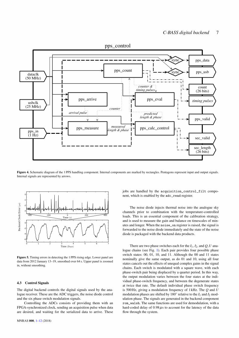
The 1 PPS signal from the GPS is crucial because it allows the re-ceived sky signal to be matched to the antenna pointing and di-agnostic signals. The C-BASS GPS system suffered from strong60Hz pickup on the 1 PPS line, which proved difficult to elimi-nate, and was strong enough to put significant jitter on to the 1 PPSrising edge. A multistep algorithm was developed which robustlydetected the 1 PPS rising edges and took a running mean of thenumber of FPGA clock cycles per GPS second through a damp-ing filter. Any discrepancies between internal timekeeping and theGPS signal were iteratively resolved, providing a stable time refer-ence, accurate to 2 µs. This algorithm is contained within the FPGAfirmware in a component called pps_control. A schematic illus-tration of pps_control and its subcomponents can be found inFig. 4. pps_control has five subcomponents:
pps_arrive Awaits the arrival of the next 1 PPS rising edge. Therising edge is only accepted if the 1 PPS line has been low for atleast 500 clock cycles prior to the rising edge and stays high for atleast 500 clock cycles following the rising edge. If these conditionsare met, then an arrival pulse is sent to pps_measure.pps_measure Upon receipt of the arrival pulse, calculates the
length of the previous second (in clock cycles) taking into accountany phase difference between the 1 PPS and internal counter, asreported by pps_measure. The measured second length and phaseare sent to pps_calc_control for use in predicting the length offuture seconds.pps_calc_control Calculates the running mean of the last
thirty-two 1-second lengths to predict the length of the next secondin clock cycles. The predicted second length and corrective phaseshift (which is the measured phase divided by 32 to avoid suddendiscontinuities) is sent to pps_count for use during the next sec-ond.
MNRAS 000, 1–12 (2018)
6 M. A. Stevenson et al.
Figure 3. Schematic diagram of the primary FPGA firmware. The components are represented as rectangles. Pentagons represent the input and output signals.Internal signals, and groups thereof, are represented by arrows. The bold lines and components mark the path of continuous data. The dot-dashed line is forburst (high time-resolution) data.
pps_count Maintains an internal counter representing the bestguess of the current time between 1 PPS arrivals. The countercounts up to the predicted second length, modified by the predictedsecond phase, as calculated by pps_calc_control. This counteris used by pps_measure to measure the current second’s length, aswell as to drive several timing pulses for use in the firmware DSPchain.pps_eval Ensures the health of the counter and timing pulses
coming from pps_count in comparison to the 1 PPS signal itself.If all appears to be well, the pps_valid flag is raised.
These five components work together in a negative feedback loopwhich is robust to noise on the 1 PPS line and quickly damps any er-rors resulting from rare failures to detect the 1 PPS rising edge. In-deed, the system is designed to work using predicted second lengths
for eight seconds in the event that no 1 PPS rising edge is detected.This is sufficient for normal operation.
The pps_valid flag is high when all is working well, and isused by the rest of the firmware to ensure proper timing. The pre-dicted second lengths are bundled with the astronomical data prod-uct and are saved in the C-BASS data archive. A sample of theseis shown in Fig. 5. It is clear from these time series that the timingvaries over the day, probably because of temperature variations ofthe backend hardware. Errors in the detection of the 1 PPS risingedge occur on 1-second timescales, but result in timing errors ofless than 2 µs and are quickly damped. These errors are small com-pared with the integration time and have negligible effect on theastronomical data.
MNRAS 000, 1–12 (2018)
C-BASS digital backend 7
Figure 4. Schematic diagram of the 1 PPS handling component. Internal components are marked by rectangles. Pentagons represent input and output signals.Internal signals are represented by arrows.
Time (Days)
Back
en
d C
lock
Err
or
(µs)
-400 -200 0 200 400Time (s)
-3
-2
-1
0
0 1 2 3 4 5 6 7
-6
-4
-2
0
Figure 5. Timing errors in detecting the 1 PPS rising edge. Lower panel aredata from 2012 January 13–19, smoothed over 64 s. Upper panel is zoomedin, without smoothing.
4.3 Control Signals
The digital backend controls the digital signals used by the ana-logue receiver. These are the ADC triggers, the noise diode controland the six phase switch modulation signals.
Controlling the ADCs consists of providing them with anFPGA-synchronized clock, sending an acquisition pulse when dataare desired, and waiting for the serialized data to arrive. These
jobs are handled by the acquisition_control_filt compo-nent, which is enabled by the adc_read register.
The noise diode injects thermal noise into the analogue skychannels prior to combination with the temperature-controlledloads. This is an essential component of the calibration strategy,and is used to measure the gain and balance on timescales of min-utes and longer. When the noise_on register is raised, the signal isforwarded to the noise diode immediately and the state of the noisediode is packaged with the backend data products.
There are two phase switches each for the I1, I2, and Q,U ana-logue chains (see Fig. 1). Each pair provides four possible phaseswitch states: 00, 01, 10, and 11. Although the 00 and 11 statesnominally give the same output, as do 01 and 10, using all fourstates cancels out the effects of unequal complex gains in the signalchains. Each switch is modulated with a square wave, with eachphase-switch pair being displaced by a quarter period. In this way,the output modulation varies between the four states at the indi-vidual phase-switch frequency, and between the degenerate statesat twice that rate. The default individual phase switch frequencyis 500Hz, giving a modulation frequency of 1kHz. The Q and Umodulation phases are shifted by 180◦ relative to the I1 and I2 mod-ulation phase. The signals are generated in the backend componentrom_walsh. The same functions are used for demodulation, with ahard-coded delay of 0.98 µs to account for the latency of the dataflow through the system.
MNRAS 000, 1–12 (2018)
8 M. A. Stevenson et al.
Figure 6. Flowchart of the continuous mode DSP, showing data bit-widthsand rates at various stages.
4.4 DSP Chain
The signal processing is split into two parallel chains, one for fil-tered and one for unfiltered data (see Section 2.2). The filtered chainis designed to give maximal rejection of systematic noise while pre-serving the astronomical signal. The unfiltered data allows somesystematic noise to pass, but preserves absolute power level infor-mation.
As described in Section 3, 14-bit data enter the FPGA via se-rial transfers from each ADC. The first step in processing the data isto convert the data from serial to parallel, which is done in the com-ponent convert_control. The data then enter the dsp_controlcomponent through the data_mux, which can also be switched toprovide simulated data instead. The unfiltered chain splits the datainto 24 channels, representing the two phase-states of each of the12 analog inputs, while the filtered chain pairwise-subtracts and de-modulates the data down to 6 channels. The unfiltered chain thenintegrates the data directly, while the filtered chain filters and down-samples the data in four stages, to achieve the final data rate of100 Hz. Finally, the outputs of the two chains are packaged to-gether and prepared for USB transfer. A flowchart of these chainsis shown in Fig. 6.
The data precision throughout the DSP chain is limited by theFPGA resources. More bits for a given data point allow higher pre-cision, but at the cost of greater resource requirements. The FPGA’smultipliers and random access memory blocks (BRAM) operatewith 18-bit data; using more than 18 bits thus requires double the
1 4 16 64 256 1024 4096 16384
Nonlinearity-Free Measurement (DU)
1
4
16
64
256
1024
4096
AD
C M
easu
rem
en
t (D
U)
Linear
Nonlinear
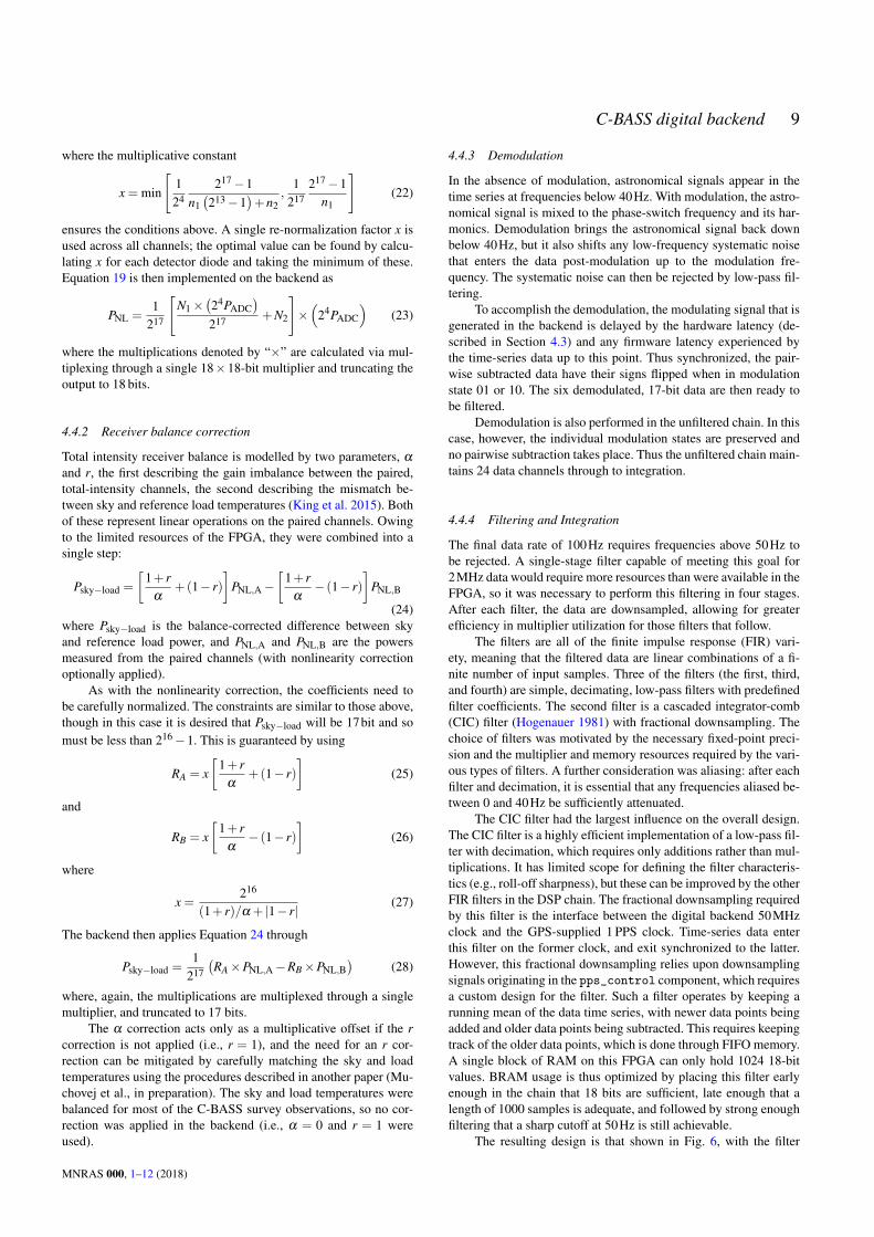
Figure 7. Sample nonlinearity curve for the detector diode of Channel 1. Alinear response is shown for comparison.
number of multipliers or RAM blocks. At the same time, truncat-ing the number of bits can introduce roundoff noise (Rabiner &Gold 1975). Care must be taken to ensure that the roundoff noiseis less than the intrinsic noise of the data, to ensure that the finalsignal-to-noise ratio is not compromised.
4.4.1 Nonlinearity correction
The integration and differencing that occurs in the filtered datachain precludes the possibility of doing certain kinds of data correc-tions off-line. These must therefore be done in the real-time system.In particular, any nonlinearity effects due to the detector diode re-sponse, as well as any multiplicative corrections required to correctreceiver balance, must be done in real time. The filter chain allowsfor these corrections in the filter_condition component, whichapplies pre-set nonlinearity and receiver balance corrections to thedata.
Detector nonlinearity is modelled as a quadratic function:
PNL = n1P2ADC +n2PADC = (n1PADC +n2)PADC (19)
where PADC is the measured power and PNL the power after non-linearity correction. These coefficients were measured for the in-dividual detector diodes in the lab. Typical values are a few times10−4 for n1 and between 0.95 and 1.05 for n2. An example curveis shown in Fig. 7. On-sky tests demonstrated that in normal astro-nomical observations nonlinearity was not detectable, as the diodeswere typically operated at relatively low power levels.
In the case where a nonlinearity correction is required, caremust be taken to ensure that the dynamic ranges of the data chan-nels are preserved. Because the arithmetic is fixed-point rather thanfloating-point, poor choice of coefficients can lead to under- orover-flow of significant bits. The 14-bit PADC inputs are made 18-bit via zero-padding the least significant bits (equivalent to multi-plying by 24). Being two’s complement, the maximum values arethen 217− 24. The maximum acceptable value of PNL is 217− 1.The value of n1 should be maximized to guarantee maximum dy-namic range, but be no greater than 217−1. These requirements aresatisfied by re-normalizing the nonlinearity coefficients via:
N1 = 217 xn1 (20)
and
N2 = 24 xn2 (21)
MNRAS 000, 1–12 (2018)
C-BASS digital backend 9
where the multiplicative constant
x = min
[124
217−1n1(213−1
)+n2
,1
217217−1
n1
](22)
ensures the conditions above. A single re-normalization factor x isused across all channels; the optimal value can be found by calcu-lating x for each detector diode and taking the minimum of these.Equation 19 is then implemented on the backend as
PNL =1
217
[N1×
(24PADC
)217 +N2
]×(
24PADC
)(23)
where the multiplications denoted by “×” are calculated via mul-tiplexing through a single 18×18-bit multiplier and truncating theoutput to 18 bits.
4.4.2 Receiver balance correction
Total intensity receiver balance is modelled by two parameters, α
and r, the first describing the gain imbalance between the paired,total-intensity channels, the second describing the mismatch be-tween sky and reference load temperatures (King et al. 2015). Bothof these represent linear operations on the paired channels. Owingto the limited resources of the FPGA, they were combined into asingle step:
Psky−load =
[1+ r
α+(1− r)
]PNL,A−
[1+ r
α− (1− r)
]PNL,B
(24)where Psky−load is the balance-corrected difference between skyand reference load power, and PNL,A and PNL,B are the powersmeasured from the paired channels (with nonlinearity correctionoptionally applied).
As with the nonlinearity correction, the coefficients need tobe carefully normalized. The constraints are similar to those above,though in this case it is desired that Psky−load will be 17bit and somust be less than 216−1. This is guaranteed by using
RA = x[
1+ rα
+(1− r)]
(25)
and
RB = x[
1+ rα− (1− r)
](26)
where
x =216
(1+ r)/α + |1− r|(27)
The backend then applies Equation 24 through
Psky−load =1
217
(RA×PNL,A−RB×PNL,B
)(28)
where, again, the multiplications are multiplexed through a singlemultiplier, and truncated to 17 bits.
The α correction acts only as a multiplicative offset if the rcorrection is not applied (i.e., r = 1), and the need for an r cor-rection can be mitigated by carefully matching the sky and loadtemperatures using the procedures described in another paper (Mu-chovej et al., in preparation). The sky and load temperatures werebalanced for most of the C-BASS survey observations, so no cor-rection was applied in the backend (i.e., α = 0 and r = 1 wereused).
4.4.3 Demodulation
In the absence of modulation, astronomical signals appear in thetime series at frequencies below 40Hz. With modulation, the astro-nomical signal is mixed to the phase-switch frequency and its har-monics. Demodulation brings the astronomical signal back downbelow 40Hz, but it also shifts any low-frequency systematic noisethat enters the data post-modulation up to the modulation fre-quency. The systematic noise can then be rejected by low-pass fil-tering.
To accomplish the demodulation, the modulating signal that isgenerated in the backend is delayed by the hardware latency (de-scribed in Section 4.3) and any firmware latency experienced bythe time-series data up to this point. Thus synchronized, the pair-wise subtracted data have their signs flipped when in modulationstate 01 or 10. The six demodulated, 17-bit data are then ready tobe filtered.
Demodulation is also performed in the unfiltered chain. In thiscase, however, the individual modulation states are preserved andno pairwise subtraction takes place. Thus the unfiltered chain main-tains 24 data channels through to integration.
4.4.4 Filtering and Integration
The final data rate of 100Hz requires frequencies above 50Hz tobe rejected. A single-stage filter capable of meeting this goal for2MHz data would require more resources than were available in theFPGA, so it was necessary to perform this filtering in four stages.After each filter, the data are downsampled, allowing for greaterefficiency in multiplier utilization for those filters that follow.
The filters are all of the finite impulse response (FIR) vari-ety, meaning that the filtered data are linear combinations of a fi-nite number of input samples. Three of the filters (the first, third,and fourth) are simple, decimating, low-pass filters with predefinedfilter coefficients. The second filter is a cascaded integrator-comb(CIC) filter (Hogenauer 1981) with fractional downsampling. Thechoice of filters was motivated by the necessary fixed-point preci-sion and the multiplier and memory resources required by the vari-ous types of filters. A further consideration was aliasing: after eachfilter and decimation, it is essential that any frequencies aliased be-tween 0 and 40Hz be sufficiently attenuated.
The CIC filter had the largest influence on the overall design.The CIC filter is a highly efficient implementation of a low-pass fil-ter with decimation, which requires only additions rather than mul-tiplications. It has limited scope for defining the filter characteris-tics (e.g., roll-off sharpness), but these can be improved by the otherFIR filters in the DSP chain. The fractional downsampling requiredby this filter is the interface between the digital backend 50MHzclock and the GPS-supplied 1 PPS clock. Time-series data enterthis filter on the former clock, and exit synchronized to the latter.However, this fractional downsampling relies upon downsamplingsignals originating in the pps_control component, which requiresa custom design for the filter. Such a filter operates by keeping arunning mean of the data time series, with newer data points beingadded and older data points being subtracted. This requires keepingtrack of the older data points, which is done through FIFO memory.A single block of RAM on this FPGA can only hold 1024 18-bitvalues. BRAM usage is thus optimized by placing this filter earlyenough in the chain that 18 bits are sufficient, late enough that alength of 1000 samples is adequate, and followed by strong enoughfiltering that a sharp cutoff at 50Hz is still achievable.
The resulting design is that shown in Fig. 6, with the filter
MNRAS 000, 1–12 (2018)
10 M. A. Stevenson et al.
properties listed in Table 3. The filters are characterized by theirpassband frequencies fpass, stopband frequencies fout, the passbandripple Apass, and the stopband attenuation Astop. The input frequen-cies, filter orders, decimation rates, and output bitwidths are alsolisted.
The first filter was designed under the limitations of using asingle multiplier/BRAM pair and providing the CIC filter with 18-bit inputs. This filter decimates by a factor of four, has a passbandbelow 40Hz, and a stopband above 499960Hz (with 100dB of re-jection). This is a rather broad filter, only requiring 15 coefficients.The output data are at a 500kHz rate and 18-bit resolution. TheCIC filter follows, with a length of 1000 samples and a decimationfactor of 25. The CIC filter’s frequency response is a sinc func-tion, which falls off only as 1/ν but has nulls at multiples of 5kHz.The choice of decimation rate thus places those frequencies aliasedto the passband at nulls in the CIC response. Further, any periodicartefacts due to the modulation itself will be nulled as well. As men-tioned above, the downsampling rate is synchronized to the 1 PPStiming so that the output data have a rate of exactly 20kHz. The fil-ter length requires an output precision of 24bit. For this filter, eachchannel requires its own BRAM, and so a total of six on the FPGAare used.
The last two filters decimate by factors of 20 and 10 respec-tively to reach the final data rate of 100Hz. Achieving the necessarystopbands at 940 and 60Hz, with attenuations of 100 and 80dB, re-quired filter lengths of 119 and 239, respectively. Output precisionsof 28bit and 30bit were used. These filters were achieved on theFPGA using 3 multipliers plus 4 blocks of RAM for the first, and3 plus 6 for the second. Altogether, the filter chain used 17 of theFPGA’s 24 multiplier/BRAM pairs.
As mentioned in Section 4.3, only a small number of modu-lation frequencies are compatible with this filter chain. There aretwo constraints. First, the modulation period must be divisible by16 to accommodate the four phase states and the first decimationby four. Second, the CIC period must be divisible by one quarter ofthe modulation period in order to guarantee removal of modulationartefacts. Eight frequencies meet these requirements and are listedin Table 4. The default was chosen as the lowest of these in orderto minimize attenuation from the detector diode video bandwidths.
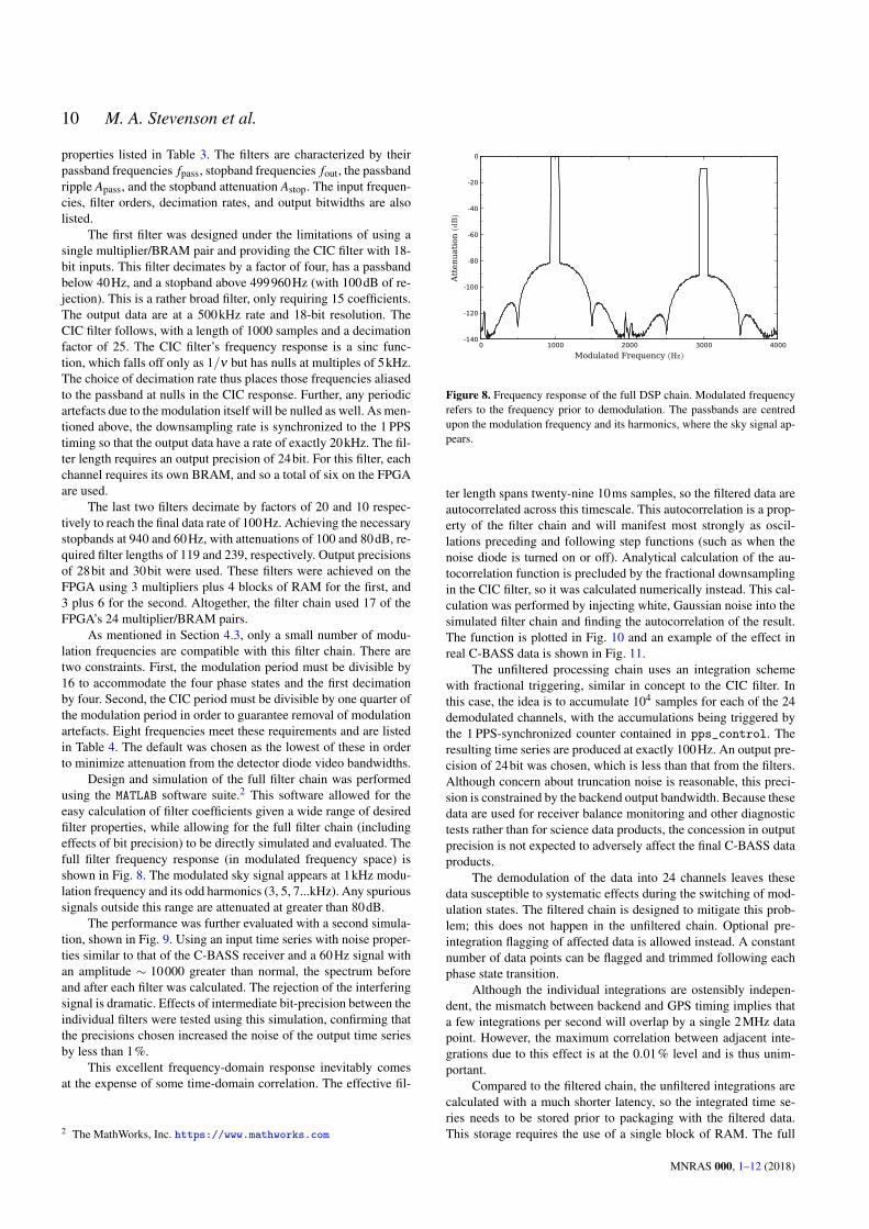
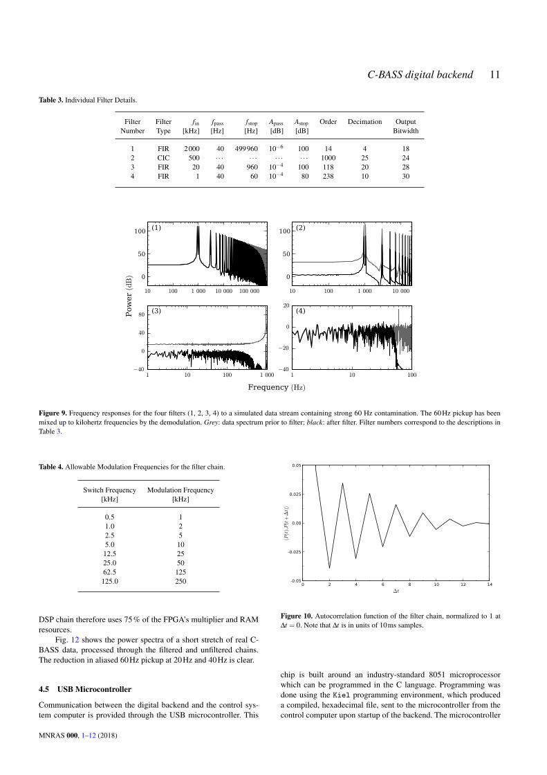
Design and simulation of the full filter chain was performedusing the MATLAB software suite.2 This software allowed for theeasy calculation of filter coefficients given a wide range of desiredfilter properties, while allowing for the full filter chain (includingeffects of bit precision) to be directly simulated and evaluated. Thefull filter frequency response (in modulated frequency space) isshown in Fig. 8. The modulated sky signal appears at 1kHz modu-lation frequency and its odd harmonics (3, 5, 7...kHz). Any spurioussignals outside this range are attenuated at greater than 80dB.
The performance was further evaluated with a second simula-tion, shown in Fig. 9. Using an input time series with noise proper-ties similar to that of the C-BASS receiver and a 60Hz signal withan amplitude ∼ 10000 greater than normal, the spectrum beforeand after each filter was calculated. The rejection of the interferingsignal is dramatic. Effects of intermediate bit-precision between theindividual filters were tested using this simulation, confirming thatthe precisions chosen increased the noise of the output time seriesby less than 1%.
This excellent frequency-domain response inevitably comesat the expense of some time-domain correlation. The effective fil-
2 The MathWorks, Inc. https://www.mathworks.com
0 1000 2000 3000 4000
Modulated Frequency (Hz)
-140
-120
-100
-80
-60
-40
-20
0
Att
en
uati
on
(dB
)
Figure 8. Frequency response of the full DSP chain. Modulated frequencyrefers to the frequency prior to demodulation. The passbands are centredupon the modulation frequency and its harmonics, where the sky signal ap-pears.
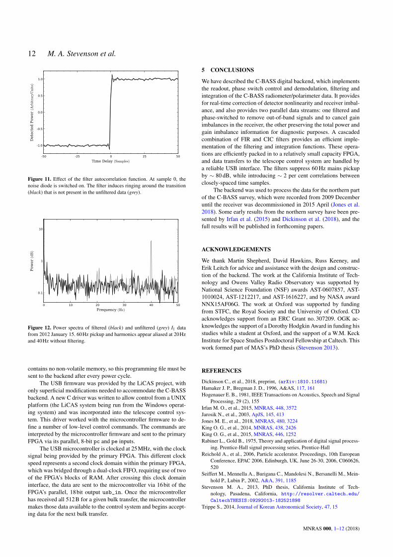
ter length spans twenty-nine 10ms samples, so the filtered data areautocorrelated across this timescale. This autocorrelation is a prop-erty of the filter chain and will manifest most strongly as oscil-lations preceding and following step functions (such as when thenoise diode is turned on or off). Analytical calculation of the au-tocorrelation function is precluded by the fractional downsamplingin the CIC filter, so it was calculated numerically instead. This cal-culation was performed by injecting white, Gaussian noise into thesimulated filter chain and finding the autocorrelation of the result.The function is plotted in Fig. 10 and an example of the effect inreal C-BASS data is shown in Fig. 11.
The unfiltered processing chain uses an integration schemewith fractional triggering, similar in concept to the CIC filter. Inthis case, the idea is to accumulate 104 samples for each of the 24demodulated channels, with the accumulations being triggered bythe 1 PPS-synchronized counter contained in pps_control. Theresulting time series are produced at exactly 100Hz. An output pre-cision of 24bit was chosen, which is less than that from the filters.Although concern about truncation noise is reasonable, this preci-sion is constrained by the backend output bandwidth. Because thesedata are used for receiver balance monitoring and other diagnostictests rather than for science data products, the concession in outputprecision is not expected to adversely affect the final C-BASS dataproducts.
The demodulation of the data into 24 channels leaves thesedata susceptible to systematic effects during the switching of mod-ulation states. The filtered chain is designed to mitigate this prob-lem; this does not happen in the unfiltered chain. Optional pre-integration flagging of affected data is allowed instead. A constantnumber of data points can be flagged and trimmed following eachphase state transition.
Although the individual integrations are ostensibly indepen-dent, the mismatch between backend and GPS timing implies thata few integrations per second will overlap by a single 2MHz datapoint. However, the maximum correlation between adjacent inte-grations due to this effect is at the 0.01% level and is thus unim-portant.
Compared to the filtered chain, the unfiltered integrations arecalculated with a much shorter latency, so the integrated time se-ries needs to be stored prior to packaging with the filtered data.This storage requires the use of a single block of RAM. The full
MNRAS 000, 1–12 (2018)
C-BASS digital backend 11
Table 3. Individual Filter Details.
Filter Filter fin fpass fstop Apass Astop Order Decimation OutputNumber Type [kHz] [Hz] [Hz] [dB] [dB] Bitwidth
1 FIR 2000 40 499960 10−6 100 14 4 182 CIC 500 · · · · · · · · · · · · 1000 25 243 FIR 20 40 960 10−4 100 118 20 284 FIR 1 40 60 10−4 80 238 10 30
10 100 1 000 10 000 100 000
0
50
100
10 100 1 000 10 000
0
50
100
1 10 100 1 000−40
0
40
80
1 10 100−40
−20
0
20
Frequency (Hz)
Pow
er
(dB
)
(1) (2)
(3) (4)
Figure 9. Frequency responses for the four filters (1, 2, 3, 4) to a simulated data stream containing strong 60 Hz contamination. The 60Hz pickup has beenmixed up to kilohertz frequencies by the demodulation. Grey: data spectrum prior to filter; black: after filter. Filter numbers correspond to the descriptions inTable 3.
Table 4. Allowable Modulation Frequencies for the filter chain.
Switch Frequency Modulation Frequency[kHz] [kHz]
0.5 11.0 22.5 55.0 10
12.5 2525.0 5062.5 125125.0 250
DSP chain therefore uses 75% of the FPGA’s multiplier and RAMresources.
Fig. 12 shows the power spectra of a short stretch of real C-BASS data, processed through the filtered and unfiltered chains.The reduction in aliased 60Hz pickup at 20Hz and 40Hz is clear.
4.5 USB Microcontroller
Communication between the digital backend and the control sys-tem computer is provided through the USB microcontroller. This
0 2 4 6 8 10 12 14
∆t
-0.05
-0.025
0.00
0.025
0.05
〈P(t
),P(t
+∆t)〉
Figure 10. Autocorrelation function of the filter chain, normalized to 1 at∆t = 0. Note that ∆t is in units of 10ms samples.
chip is built around an industry-standard 8051 microprocessorwhich can be programmed in the C language. Programming wasdone using the Kiel programming environment, which produceda compiled, hexadecimal file, sent to the microcontroller from thecontrol computer upon startup of the backend. The microcontroller
MNRAS 000, 1–12 (2018)
12 M. A. Stevenson et al.
-50 -25 0 25 50
Time Delay (Samples)
-1.0
-0.5
0.0
0.5
1.0
Dete
cted
Pow
er
(Arb
itra
ryU
nits)
Figure 11. Effect of the filter autocorrelation function. At sample 0, thenoise diode is switched on. The filter induces ringing around the transition(black) that is not present in the unfiltered data (grey).
0 10 20 30 40 50
Frequency (Hz)
0.1
1
10
Pow
er
(dB
)
Figure 12. Power spectra of filtered (black) and unfiltered (grey) I1 datafrom 2012 January 15. 60Hz pickup and harmonics appear aliased at 20Hzand 40Hz without filtering.
contains no non-volatile memory, so this programming file must besent to the backend after every power cycle.
The USB firmware was provided by the LiCAS project, withonly superficial modifications needed to accommodate the C-BASSbackend. A new C driver was written to allow control from a UNIXplatform (the LiCAS system being run from the Windows operat-ing system) and was incorporated into the telescope control sys-tem. This driver worked with the microcontroller firmware to de-fine a number of low-level control commands. The commands areinterpreted by the microcontroller firmware and sent to the primaryFPGA via its parallel, 8-bit pc and pe inputs.
The USB microcontroller is clocked at 25MHz, with the clocksignal being provided by the primary FPGA. This different clockspeed represents a second clock domain within the primary FPGA,which was bridged through a dual-clock FIFO, requiring use of twoof the FPGA’s blocks of RAM. After crossing this clock domaininterface, the data are sent to the microcontroller via 16bit of theFPGA’s parallel, 18bit output usb_in. Once the microcontrollerhas received all 512B for a given bulk transfer, the microcontrollermakes those data available to the control system and begins accept-ing data for the next bulk transfer.
5 CONCLUSIONS
We have described the C-BASS digital backend, which implementsthe readout, phase switch control and demodulation, filtering andintegration of the C-BASS radiometer/polarimeter data. It providesfor real-time correction of detector nonlinearity and receiver imbal-ance, and also provides two parallel data streams: one filtered andphase-switched to remove out-of-band signals and to cancel gainimbalances in the receiver, the other preserving the total power andgain imbalance information for diagnostic purposes. A cascadedcombination of FIR and CIC filters provides an efficient imple-mentation of the filtering and integration functions. These opera-tions are efficiently packed in to a relatively small capacity FPGA,and data transfers to the telescope control system are handled bya reliable USB interface. The filters suppress 60 Hz mains pickupby ∼ 80 dB, while introducing ∼ 2 per cent correlations betweenclosely-spaced time samples.
The backend was used to process the data for the northern partof the C-BASS survey, which were recorded from 2009 Decemberuntil the receiver was decommissioned in 2015 April (Jones et al.2018). Some early results from the northern survey have been pre-sented by Irfan et al. (2015) and Dickinson et al. (2018), and thefull results will be published in forthcoming papers.
ACKNOWLEDGEMENTS
We thank Martin Shepherd, David Hawkins, Russ Keeney, andErik Leitch for advice and assistance with the design and construc-tion of the backend. The work at the California Institute of Tech-nology and Owens Valley Radio Observatory was supported byNational Science Foundation (NSF) awards AST-0607857, AST-1010024, AST-1212217, and AST-1616227, and by NASA awardNNX15AF06G. The work at Oxford was supported by fundingfrom STFC, the Royal Society and the University of Oxford. CDacknowledges support from an ERC Grant no. 307209. OGK ac-knowledges the support of a Dorothy Hodgkin Award in funding hisstudies while a student at Oxford, and the support of a W.M. KeckInstitute for Space Studies Postdoctoral Fellowship at Caltech. Thiswork formed part of MAS’s PhD thesis (Stevenson 2013).
REFERENCES
Dickinson C., et al., 2018, preprint, (arXiv:1810.11681)Hamaker J. P., Bregman J. D., 1996, A&AS, 117, 161Hogenauer E. B., 1981, IEEE Transactions on Acoustics, Speech and Signal
Processing, 29 (2), 155Irfan M. O., et al., 2015, MNRAS, 448, 3572Jarosik N., et al., 2003, ApJS, 145, 413Jones M. E., et al., 2018, MNRAS, 480, 3224King O. G., et al., 2014, MNRAS, 438, 2426King O. G., et al., 2015, MNRAS, 446, 1252Rabiner L., Gold B., 1975, Theory and application of digital signal process-
ing. Prentice-Hall signal processing series, Prentice-HallReichold A., et al., 2006, Particle accelerator. Proceedings, 10th European
Conference, EPAC 2006, Edinburgh, UK, June 26-30, 2006, C060626,520
Seiffert M., Mennella A., Burigana C., Mandolesi N., Bersanelli M., Mein-hold P., Lubin P., 2002, A&A, 391, 1185
Stevenson M. A., 2013, PhD thesis, California Institute of Tech-nology, Pasadena, California, http://resolver.caltech.edu/CaltechTHESIS:09292013-182521898
Trippe S., 2014, Journal of Korean Astronomical Society, 47, 15
MNRAS 000, 1–12 (2018)