Embed Size (px)
Citation preview
Purdue UniversityPurdue e-Pubs
ECE Technical Reports Electrical and Computer Engineering
4-1-1996
THE ANALYSIS, SIMULATION, ANDIMPLEMENTATION OF CONTROLSTRATEGIES FOR A PULSEWIDTHMODULATED INDUCTION MOTORDRIVEScott D. RollerPurdue University School of Electrical and Computer Engineering
Chee Mun OngPurdue University School of Electrical and Computer Engineering
Follow this and additional works at: http://docs.lib.purdue.edu/ecetrPart of the Electrical and Computer Engineering Commons
This document has been made available through Purdue e-Pubs, a service of the Purdue University Libraries. Please contact [email protected] foradditional information.
Roller, Scott D. and Ong, Chee Mun, "THE ANALYSIS, SIMULATION, AND IMPLEMENTATION OF CONTROLSTRATEGIES FOR A PULSEWIDTH MODULATED INDUCTION MOTOR DRIVE" (1996). ECE Technical Reports. Paper 101.http://docs.lib.purdue.edu/ecetr/101
THE ANALYSIS, SIMULATION, AND
IMPLEMENTATION OF CONTROL
STRATEGIES FOR A PULSEWIDTH
MOD~~LATED INDUCTION MOTOR
DRIVE
TR-ECE 96-7 APRIL 1996
THE ANALYSIS. SIMULATION
AND IMPLEMENTATION OF
CONTROL STRATEGIES FOR
A PULSEWIDTH MODCTLATED
INDUCTION MOTOR DRIVE
by
Scott D. Roller
Professor Chee-Mun Ong
Purdue Electric Power Center
School of Electrical Engineering
Purdue University
1285 Electrical Engineering Building
West Lafayette, IN 47907- 1285
May 1996

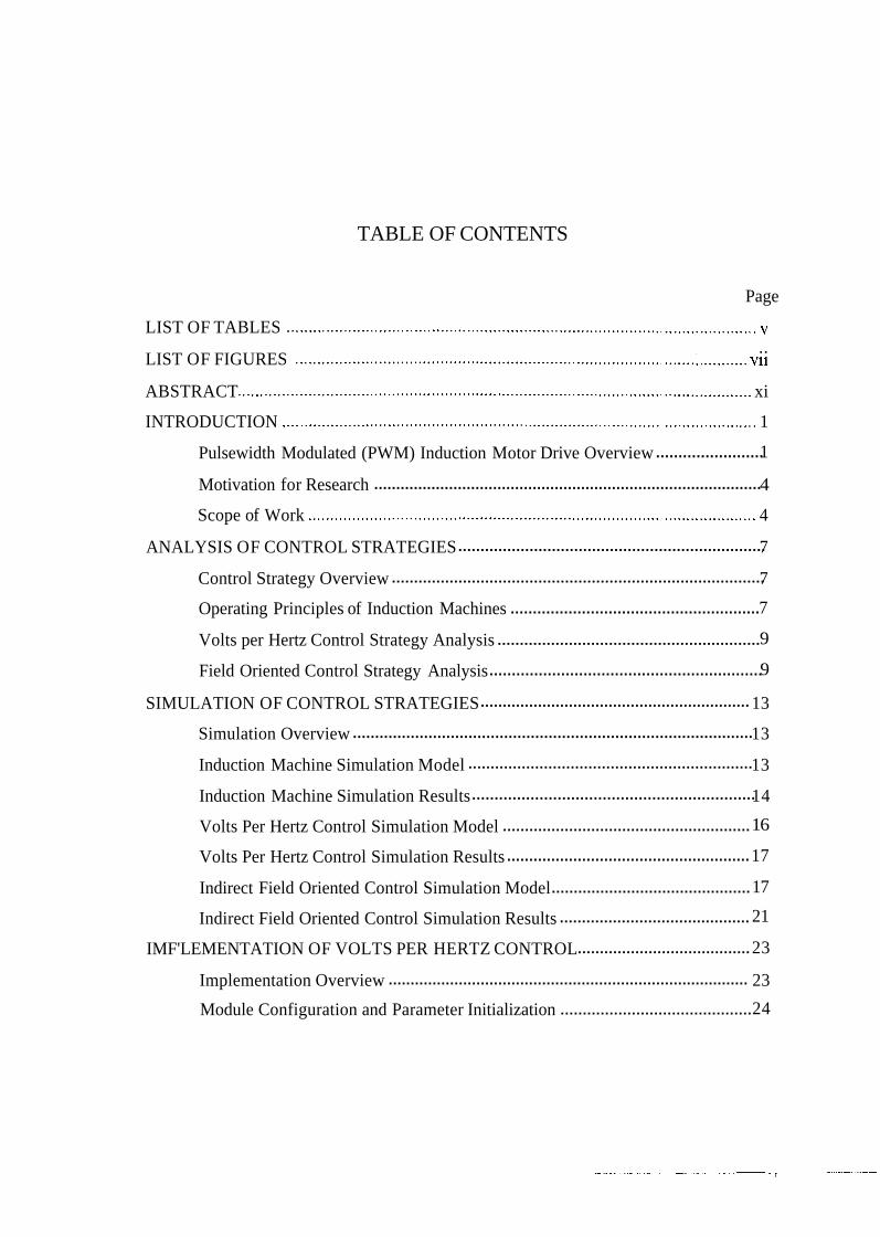
TABLE OF CONTENTS
Page
LIST OF TABLES ........................................................................................................... v . .
LIST OF FIGURES ........................................................................................... : ........... vii
ABSTRACT ..................................................................................................................... xi
INTRODUCTION ............................................................................................................ 1
........................ Pulsewidth Modulated (PWM) Induction Motor Drive Overview 1
........................................................................................ Motivation for Research 4
Scope of Work ....................................................................................................... 4
..................................................................... ANALYSIS OF CONTROL STRATEGIES 7
.................................................................................... Control Strategy Overview 7
........................................................ Operating Principles of Induction Machines 7
........................................................... Volts per Hertz Control Strategy Analysis 9
............................................................. Field Oriented Control Strategy Analysis 9
............................................................. SIMULATION OF CONTROL STRATEGIES 13
.......................................................................................... Simulation Overview 13
................................................................ Induction Machine Simulation Model 13
............................................................... Induction Machine Simulation Results 14
........................................................ Volts Per Hertz Control Simulation Model 16
....................................................... Volts Per Hertz Control Simulation Results 17
............................................. Indirect Field Oriented Control Simulation Model 17
........................................... Indirect Field Oriented Control Simulation Results 21
....................................... IMF'LEMENTATION OF VOLTS PER HERTZ CONTROL 23
.................................................................................. Implementation Overview 23
........................................... Module Configuration and Parameter Initialization 24
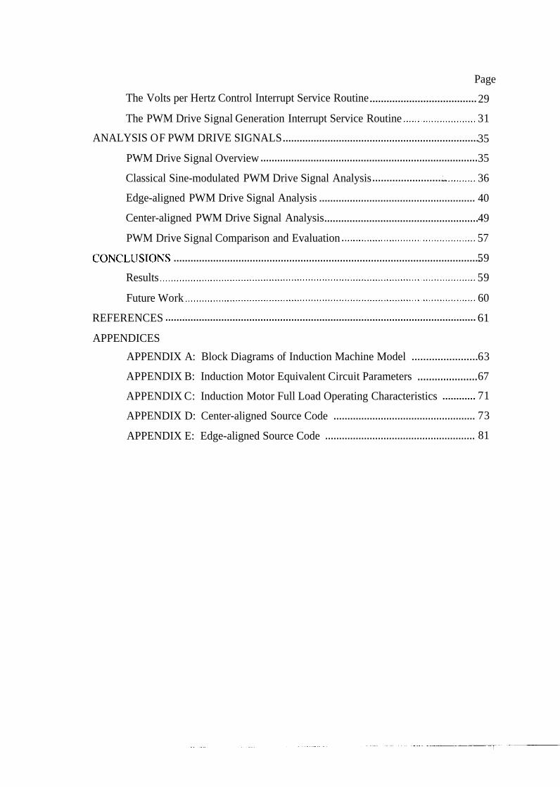
Page
...................................... The Volts per Hertz Control Interrupt Service Routine 29
The PWM Drive Signal Generation Interrupt Service Routine .......................... 31
...................................................................... ANALYSIS OF PWM DRIVE SIGNALS 35
.............................................................................. PWM Drive Signal Overview 35
.......................... Classical Sine-modulated PWM Drive Signal Analysis ; ........... 36
........................................................ Edge-aligned PWM Drive Signal Analysis 40
....................................................... Center-aligned PWM Drive Signal Analysis 49
PWM Drive Signal Comparison and Evaluation ................................................. 57
............................................................................................................. COPKLUSIONS 59
Results .................................................................................................................. 59
Future Work ......................................................................................................... 60
............................................................................................................... REFERENCES 61
APPENDICES
....................... APPENDIX A: Block Diagrams of Induction Machine Model 63
..................... APPENDIX B: Induction Motor Equivalent Circuit Parameters 67
............ APPENDIX C: Induction Motor Full Load Operating Characteristics 71
................................................... APPENDIX D: Center-aligned Source Code 73
...................................................... APPENDIX E: Edge-aligned Source Code 81

LIST OF TABLES
Tab1.e Page
............................................... 4.1. Program variables. definitions and initial values 27
4.2. User defined exception vectors and associated vector assignments .................. 27
........... 5.1. Spectra analysis of the classical sine-modulated PWMAB drive signal 40
.............................. 5.2. Spectra analysis of the edge-aligned PWMAB drive signal 47
............................ 5.3. Spectra analysis of the center-aligned PWMAB drive signal 52
5.4. Spectra Analysis of the classical. center-aligned and edge-aligned PWM drive
signals ............................................................................................................... 58


LIST OF FIGURES
Figure Page
1.1. Block diagram of an induction motor drive system ............................................ 1
1.2. Schematic diagram of a three phase variable frequency converter,
including the full-wave rectifier, DC link and voltage-source inverter. .............. 2
1.3. Classical PWM drive signals for a three phase sine-modulated
PWM voltage-source inverter. ............................................................................. 3
2.1. The per phase equivalent circuit of a singly excited induction machine. ............ 8
2.2. Block diagram of the closed loop volts per hertz control strategy. ..................... 9
2.3. Graphical representation of the relationship between the stator anti
rotor abc reference frames and the synchronously rotating qdO ref0 ,rence
frame of the rotor when the rotor flux is properly aligned. ............................... 12
2.4. Block Diagram of the indirect field oriented control strategy. .......................... 12
3.1. Block diagram of the simulation model for an induction motor ........................ 14
3.2. Plots of the electromagnetic torque and stator current versus mechanical
rotor speed for an induction motor operating under no control. ........................ 15
3.3. Plots of the electromagnetic torque and rotor flux versus time for
an induction motor operating under no control. ................................................ 15
3.4. Block diagram of the simulation model for the closed loop volts per
hertz control strategy. . . . .. .. .. .. .. .. .. .. .. .. .. ... .. .. .. .. .. . . . . . . . . . . . . . . . . . . . . 16
3.5. Plots of the electromagnetic torque and stator current versus mechanical
rotor speed for the simulation model of an induction motor operating
under closed loop volts per hertz control. ............ .......................... ...... .............. 18
3.6. Block diagram of the indirect field oriented control simulation model. ............ 19

Figure Page
3.7. Block diagram of the calcs block for the indirect field oriented cointrol simulation
model ................................................................................................................. 20
3.8. Block diagram of the qde2abc block for the indirect field oriented
control simulation model ................................................................................... 20
3.9. Plots of the electromagnetic torque and rotor flux versus time for
the simulation model of an induction motor operating under indirect
field oriented control ......................................................................................... 21
4.1. Flow diagram of induction motor drive system source code ............................. 25
.................... 4.2. Flow Diagram of volts per hertz control interrupt service routine 30
4.3. Algorithm for generating the three balanced PWM drive signal high times ..... 34
5.1. Classical sine-modulated PWMA, PWMB and PWMAB drive signals.
....................................................... (fcarrier= 1000 Hz. fref= 100 Hz. ma=0.90) 37
5.2. Spectra analysis of the classical sine-modulated PWMAB drive signal
.................................................................. with a reference frequency of 30 Hz 38
5.3. Spectra analysis of the classical sine-modulated PWMAB drive signal
.................................................................. with a reference frequency of 60 Hz 38
5.4. Spectra analysis of the classical sine-modulated PWMAB drive signal
.................................................................. with a reference frequency of 90 Hz 39
5.5. Spectra analysis of the classical sine-modulated PWMAB drive signal
..................................... carrier harmonics with a reference frequency of 90 Hz 39
5.6. External logic and subtraction circuit. edge-aligned mode ................................ 42
5.7. High time update timing diagram. edge-aligned mode .................................... 42
5.8. Edge-aligned PWMA, PWMB and PWMABdrive signals.
....................................................................... (fcarrier= 1000 Hz. fref= 100 Hz) 43
5.9. Edge-aligned PWMA. PWMB and PWMAB drive signals.
.................................................................... (fcarrier= 16.384 kHz. fref=30 Hz) 43
5.10. Edge-aligned PWMA. PWMB and PWMAB drive signals.
.................................................................... (farrier= 16.384 kHz. fref=60 Hz) 44
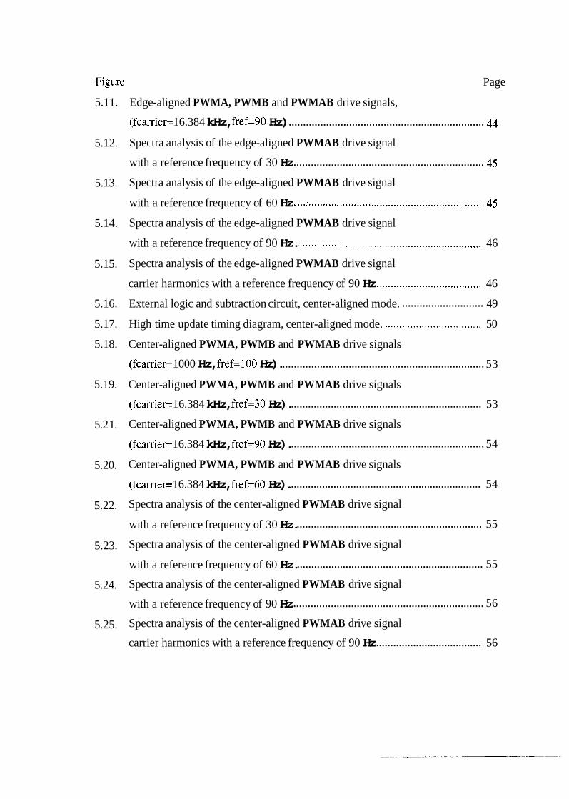
Figure Page
5.11. Edge-aligned PWMA, PWMB and PWMAB drive signals,
.................................................................... (fcarrier= 16.384 kHz, fref=90 Hz) 44
5.12. Spectra analysis of the edge-aligned PWMAB drive signal
.................................................................. with a reference frequency of 30 Hz 45
5.13. Spectra analysis of the edge-aligned PWMAB drive signal
.... ............................................................. with a reference frequency of 60 Hz : 45
5.14. Spectra analysis of the edge-aligned PWMAB drive signal
with a reference frequency of 90 Hz. ................................................................. 46
5.15. Spectra analysis of the edge-aligned PWMAB drive signal
carrier harmonics with a reference frequency of 90 Hz ..................................... 46
............................ 5.16. External logic and subtraction circuit, center-aligned mode. 49
5.17. High time update timing diagram, center-aligned mode. .................................. 50
5.18. Center-aligned PWMA, PWMB and PWMAB drive signals
...................................................................... (fcarrier= 1000 Hz, fref=100 Hz). 53
5.19. Center-aligned PWMA, PWMB and PWMAB drive signals
................................................................... (fcarrier= 16.384 kHz, fref=30 Hz). 53
5.2 1. Center-aligned PWMA, PWMB and PWMAB drive signals
................................................................... (fcarrier= 16.384 kHz, fref=90 Hz). 54
5.20. Center-aligned PWMA, PWMB and PWMAB drive signals
................................................................... (fcarrier= 16.384 kHz, fref=60 Hz). 54
5.22. Spectra analysis of the center-aligned PWMAB drive signal
................................................................. with a reference frequency of 30 Hz. 55
5.23. Spectra analysis of the center-aligned PWMAB drive signal
................................................................. with a reference frequency of 60 Hz. 55
5.24. Spectra analysis of the center-aligned PWMAB drive signal
.................................................................. with a reference frequency of 90 Hz 56
5.25. Spectra analysis of the center-aligned PWMAB drive signal
..................................... carrier harmonics with a reference frequency of 90 Hz 56

Figure Page
A . 1 . Induction machine block diagram ...................................................................... 63
A.2. abc2qds block diagram ...................................................................................... 64
A.3. Q-axis block diagram .......................................................................................... 64
A.4. D-axis block diagram ......................................................................................... 65
A.5. Rotor block diagram .......................................................................................... 65
A.6. qds2abc block diagram ...................................................................................... 66
........... B . 1 The per phase equivalent circuit of a singly excited induction machine 69
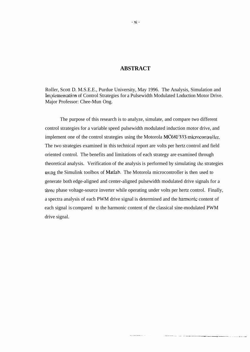
ABSTRACT
Roller, Scott D. M.S.E.E., Purdue University, May 1996. The Analysis, Simulation and Iml?lementation of Control Strategies for a Pulsewidth Modulated Lnduction Motor Drive. Major Professor: Chee-Mun Ong.
The purpose of this research is to analyze, simulate, and compare two different
control strategies for a variable speed pulsewidth modulated induction motor drive, and
implement one of the control strategies using the Motorola MC68F333 inicrocontroller.
The two strategies examined in this technical report are volts per hertz control and field
oriented control. The benefits and limitations of each strategy are examined through
theoretical analysis. Verification of the analysis is performed by simulating thc strategies
usmg the Simulink toolbox of Matlab. The Motorola microcontroller is then used to
generate both edge-aligned and center-aligned pulsewidth modulated drive signals for a
three phase voltage-source inverter while operating under volts per hertz control. Finally,
a spectra analysis of each PWM drive signal is determined and the hamionic content of
each signal is compared to the harmonic content of the classical sine-modulated PWM
drive signal.

1. INTRODUCTION
1.1 Pulsewidth Modulated (PWM) Induction Motor Drive Overview
The advent of high power, fast switching devices and fast microprocessors has
facjlitated the growth of variable spced induction motor drive systems. An induction
motor drive system is comprised of a variable frequency converter, a coritroller and an
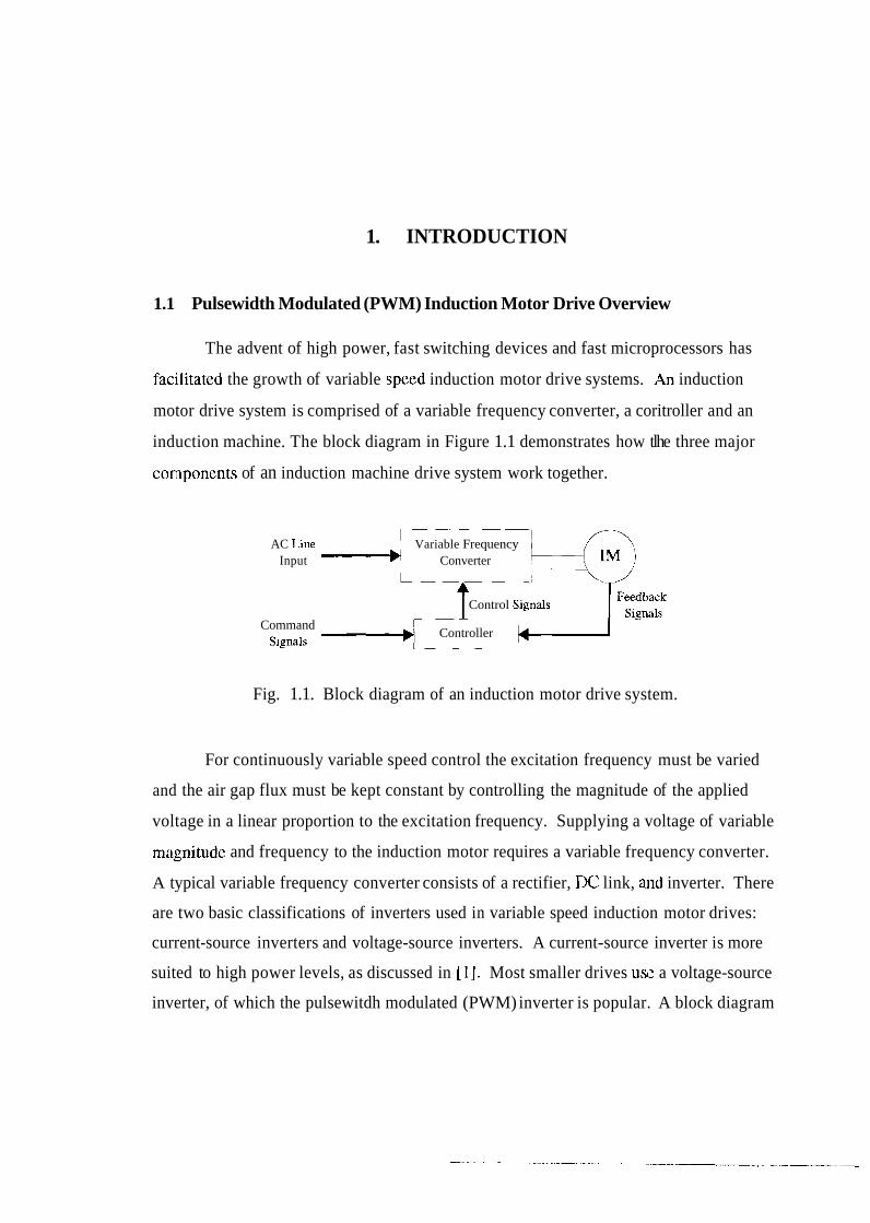
induction machine. The block diagram in Figure 1.1 demonstrates how tlhe three major
components of an induction machine drive system work together.
AC Line Variable Frequency Input Converter
Control S~gnals
Command Controller
Slgnals
Fig. 1.1. Block diagram of an induction motor drive system.
For continuously variable speed control the excitation frequency must be varied
and the air gap flux must be kept constant by controlling the magnitude of the applied
voltage in a linear proportion to the excitation frequency. Supplying a voltage of variable
magnitude and frequency to the induction motor requires a variable frequency converter.
A typical variable frequency converter consists of a rectifier, DC link, and inverter. There
are two basic classifications of inverters used in variable speed induction motor drives:
current-source inverters and voltage-source inverters. A current-source inverter is more
suited to high power levels, as discussed in [I]. Most smaller drives us!: a voltage-source
inverter, of which the pulsewitdh modulated (PWM) inverter is popular. A block diagram
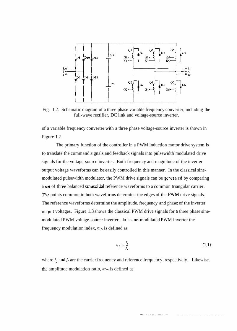
Fig. 1.2. Schematic diagram of a three phase variable frequency converter, including the full-wave rectifier, DC link and voltage-source inverter.
of a variable frequency converter with a three phase voltage-source inverter is shown in
Figure 1.2.
The primary function of the controller in a PWM induction motor drive system is
to translate the command signals and feedback signals into pulsewidth modulated drive
signals for the voltage-source inverter. Both frequency and magnitude of the inverter
output voltage waveforms can be easily controlled in this manner. In the classical sine-
modulated pulsewidth modulator, the PWM drive signals can be general.ed by comparing
a set of three balanced sinusoidal reference waveforms to a common triangular carrier.
Th: points common to both waveforms determine the edges of the PWM drive signals.
The reference waveforms determine the amplitude, frequency and phase: of the inverter
ou'.put voltages. Figure 1.3 shows the classical PWM drive signals for a three phase sine-
modulated PWM voltage-source inverter. In a sine-modulated PWM inverter the
frequency modulation index, mf, is defined as
where f, and& are the carrier frequency and reference frequency, respectively. Likewise.
thr: amplitude modulation ratio, ma, is dcfincd as
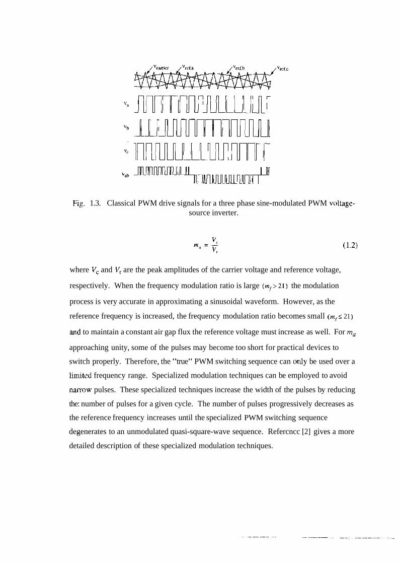
Fig. 1.3. Classical PWM drive signals for a three phase sine-modulated PWM voltage- source inverter.
where V, and V, are the peak amplitudes of the carrier voltage and reference voltage,
respectively. When the frequency modulation ratio is large (if 1 2 1 ) the modulation
process is very accurate in approximating a sinusoidal waveform. However, as the
reference frequency is increased, the frequency modulation ratio becomes small (mf s 21 )
anti to maintain a constant air gap flux the reference voltage must increase as well. For m,
approaching unity, some of the pulses may become too short for practical devices to
switch properly. Therefore, the "true" PWM switching sequence can only be used over a
limited frequency range. Specialized modulation techniques can be employed to avoid
narrow pulses. These specialized techniques increase the width of the pulses by reducing
the: number of pulses for a given cycle. The number of pulses progressively decreases as
the reference frequency increases until the specialized PWM switching sequence
degenerates ,- to an unmodulated quasi-square-wave sequence. Refercncc [2] gives a more
detailed description of these specialized modulation techniques.
1.2 Motivation for Research
From the preceding section it is obvious that complex control strategies are
required to control the speed of an induction machine. The motivation behind this
research was to gain experience and understanding of the problems associated with an
implementation of a variable speed PWM induction motor drive system. The two control
strategies that are focused on in this thesis are the volts per hertz and field oriented control.
The research involved two phases. The first was to simulate and evaluate the
performance of the volts per hertz and field oriented control strategies. The second was to
implement the volts per hertz control strategy on the Motorola MC68F333
microcontroller. The benefits and limitations of each algorithm were examined through
theoretical analysis. Verification of the analysis was performed by simulating the
strategies using the SimuLink toolbox of Matlab. The MC68F333 was then used to
generate both edge-aligned and center-aligned pulsewidth modulated drive signals for a
three phase voltage source inverter while operating under volts per hertz control. Finally,
a spectra analysis of each PWM drive signal was determined and the harmonic content of
each signal was compared to the harmonic content of the classical sine-modulated PWM
drive signal. From this comparison the performance of the edge-aligned and the center-
aligned drive signals could be evaluated.
1.3 Scope of Work
The thesis begins by analyzing the volts per hertz and field oriented control
strategies. The volts per hertz control attempts to keep the stator flux constant while the
field oriented control attempts to keep the rotor flux unperturbed. The volts per hertz
cointrol is a simple scalar control scheme whereas the field oriented control is a vector
control scheme. The benefits and limitations of each control strategy are drawn out
through the theoretical analysis and are discussed in Chapter 2.
The theoretical analysis of each control strategy is verified through simulation
using the Simulink toolbox of Matlab and is discussed in Chapter 3. Thl? induction
machine operating under no control was first simulated to establish a reference to which

the performance of the control strategies could be measured. Each of the control strategies
were then simulated and evaluated.
Chapters 4 discusses the implementation of the volts per hertz control strategy in a
PWM drive and the generation of edge-aligned and center-aligned sine-modulated PWM
drive signals on the Motorola MC68F333 microcontroller. The MC68F333 is a modular
microcontroller with a 68000-based instruction set and is ideally suited for many motor
control applications. The features of the MCU which are critical to the induction motor
drive system are the Time Processor Unit (TPLT), the Table Look-up and Interpolate
(TB'L) instruction and the capability of the processor to operate at a high clock frequency
of 16.777 MHz
A spectra analysis of the edge-aligned and center-aligned PWM drive signals
generated by the MC68F333 microcontroller is presented in Chapter 5. 'The frequency
spectrum of the classical sine-modulated PWM drive signal is also analyzed to serve as a
benchmark for the other two drive signals. The chapter ends with an evaluation of each
drive signal based on the spectra analysis.


2. ANALYSIS OF CONTROL STRATEGIES
2.1 Control Strategy Overview
The speed of the induction machine can be controlled by adjusting the magnitude
ancl frequency of the applied stator voltages. The specific control strategy implemented is
dependent on the requirements of the specific application. Two different control
strategies, volts per hertz control and field oriented control, are analyzedl in this chapter.
Thl: benefits and limitations of each control strategy are then drawn out from the
theoretical analysis.
2.2, Operating Principles of Induction Machines
A brief overview of induction machine operating principles is required before the
spt:cific control strategies can be analyzed. For a more complete discus,sion on this topic
refer to [3] and [4].
For a small value of slip, the rotor speed of an induction machine is approximately
proportional to the excitation frequency, o), . For full benefit of the iron provided, the air
gap flux, I.,, , should be maintained at its rated value. When the air gap flux is maintained
at its rated value the motor is capable of producing its rated torque and ~:xcessive
saiiuration does not occur.
The air gap flux rotates at a synchronous speed relative to the stator windings
establishing an emf which is commonly referred to as the air gap voltage, E,, . This is
illustrated in the per phase equivalent circuit for a singly excited induction machine
shown in Figure 2.1. From magnetic circuit analysis it can be shown th~at

., "
Fig. 2.1. The per phase equivalent circuit of a singly excited induction machine.
Thus, maintaining a constant air gap flux requires that the ratio of the magnetizing voltage
to t.he excitation frequency be constant. When the machine is singly excited, we can see
from Figure 2.1 that the square of the referred rotor current can be expre:ssed by the
following equation.
Equation (2.2) can then be substituted into the electromechanical torque equation for a
singly excited P-pole induction machine as shown in Equation (2.3)
Fr'om this equation, it is obvious that when the air gap flux is held cons1,ant the
electromechanical torque becomes a function of only the slip speed. Thus, if the slip
speed is maintained at a constant value then the torque will also remain constant as the
excitation frequency, a,, varies. Likewise, the rotor current remains constant as 0, varies
if the slip speed is maintained at a constant value.
voltslhertz DC Bus, control I I
speed controller
voltage luniter
. .- "" 1 Phase T".,,.+,
slip limiter I W r m
Fig. 2.2. Block diagram of the closed loop volts per hertz contrc~l strategy.
2.3 Volts per Hertz Control Strategy Analysis
In the volts per hertz strategy, the air gap flux is kept reasonably constant over the
cor~stant torque region by keeping the ratio of stator voltage to excitation frequency
constant if the stator impedance is small or the air gap voltage is close to the input voltage
applied to the stator. However, at low frequencies the stator resistance becomes dominant
ant1 the voltage drop across the stator is no longer negligible. Therefore, a low frequency
voltage boost is required to compensate for the voltage drop across the stator resistance.
Thl: volts per hertz control is often referred to as a scalar control strategy.
If a small variation in rotor speed with a change in loading is tolt:rable, then a
simple open loop control strategy would probably suffice. However, if the application
requires a tighter control over rotor speed and torque while limiting stator current, then a
clclsed loop control strategy with rotor speed as feedback is the better alternative. With
rotor speed as feedback, the slip speed of the motor can be regulated. The block diagram
for. the volts per hertz control strategy is shown in Figure 2.2.
2.41 Field Oriented Control Strategy Analysis
The field oriented control strategy allows very precise and rapid control of the
e1~;ctromechanical torque produced by an induction machine. The torque control is

accomplished by varying the stator current in such a way as to produce the amount of
torque commanded while at the same time keeping the rotor field constant. However, the
control of the rotor field is made more difficult by the interaction of the rotating stator and
rotor magnetic fields and is not easily controlled in the abc reference frame. Therefore, a
transformation to a synchronously rotating qdO reference frame whose d--axis is aligned
wit11 the rotor field is required. In such a reference frame, the q compont:nt of the rotor
field, hlEr , is zero. When proper alignment of the reference frame occurs, the torque
equation reduces to the following.
It can be seen from the equation above that the torque can be controlled by adjusting either
the rotor flux or stator current. Because the time constant of the rotor is usually large
cornpared to the stator time constant, the torque response to a change in the rotor field will
be ,very sluggish. On the other hand, the torque response to a change in the stator current
will be very rapid. Hence, the objective of the field oriented control strategy is to maintain
a constant rotor flux while controlling the torque by adjusting the q component of the
stal.or current.
In a direct field oriented control system the air gap flux is measured directly
through the use of embedded search coils or Hall-effect sensors. This approach is not
usually used in industry because the search coils are unable to measure the rotor field at
low frequencies without integrator drift, the Hall devices are temperature sensitive and
fragile and neither device is easily installed or maintained. The reader sk~ould note that the
air gap flux measured by this method is not the flux linking the rotor winding, but rather
the mutual flux between the rotor and the stator. However, the measured air gap flux,
along with the measured stator current, can be used to determine the magnitude of the
rotor flux and the position of the properly oriented qdO reference frame, as discussed in
P I . Indirect field orientation does not rely on direct measurement of the air gap flux,
but instead uses the q and d components of the stator currents and the rotor speed to

control the rotor flux indirectly and maintain proper orientation of the qdO reference
franne. This control strategy is excellent for low speed operations and for motion control
applications. However, some machine parameters, in particular the rotor resistance, may
vayj with temperature and loading of the machine. This variation in machine parameters
degrades the effectiveness of the control strategy. In practice, on-line parameter
adaptation techniques are employed to compensate for the parameter variation.
It has been shown in [3] that for a given command value of rotor fl!ux, the regulated
value of i:, is defined as follows.
It was also shown that the regulated value of i;, is proportional to the torque command
vali~e and inversely proportional to the rotor flux command value as shown below.
The regulated values of ii, and izJ can then be used to calculate the slip speed necessary to
mamtain the proper alignment of the synchronously rotating qdO reference frame with the
rotor flux as shown in the equation below.
Figure 2.3 shows the relationship between the properly oriented synchronously
rotating qdO reference frame and the stator and rotor abc reference frames. The field
orir:ntation, p, is the sum of the rotor angular position, O r , and the integral of the slip
speed, 0 2 . A block diagram of the indirect field oriented control strategy is shown in
Figure 2.4.
me
n stator field
rotor field
f rotor phase a axis
stator + phasea
axis
rotor field d-axis
Fiig. 2.3. Graphical representation of the relationship between the stator and rotor abc reference frames and the synchronously rotating qdO reference frame of he rotor when the
rotor flux is properly aligned.
speed ,DC Bus, controller --
I i * s, - -- PW=' Three
Phase -- Inverter
b
P field
weakening 8
I Ils
+
+ 1
Fig. 2.4. Block Diagram of the indirect field oriented control strategy.

3. SIMULATION OF CONTROL STRATEGIES
3.1 Simulation Overview
The theoretical analysis of the volts per hertz and field oriented control strategies
are verified through simulation using the Simulink toolbox of Matlab. The simulation of
the induction machine operating under no control was first examined to establish a frame
of reference from which the performance of each control strategy could be measured.
Simulating the three phase voltage-source inverter along with the induction
machine and the associated control strategy would be very costly in terrns of simulation
model complexity and amount of time required for a simulation run. To reduce the model
complexity time required per simulation run, a sine wave of variable fre:qucncy and
magnitude was used to approximate the fundamental component of the voltage-source
inverter output waveform. Although simulation of the voltage source inverter is possible,
it is not necessary in evaluating the performance of the control strategies since power
transfer is primarily through the fundamental component of the inverter output waveform.
3.2 Induction Machine Simulation Model
The simulation model used to evaluate the induction machine under no control
consists of a three phase induction machine block and a three phase voltage source. The
complete simulation model is shown in Figure 3.1. The model for the jnduction machine
block is shown in Appendix A and a complete analysis of the machine is given in [3]. The
actual machine simulated by the model was the MagneTek 1/4 HP Century AC Motor.
This machine has a voltage rating of 200-230 volts and a current rating of 1.1-1.4 amperes
mhen excited at a frequency of 60 Hz. The equivalent circuit parameter calculations and
full load operating characteristics for this machine are detailed in Appendices B and C,
respectively.
.I 1 L.3Mub~l Vcs
us
Irdztbn Machine
Fig. 3.1. Block diagram of the simulation model for an induction motor.
3.3 Induction Machine Simulation Results
For the first simulation run, the induction machine was excited at its rated voltage
and frequency (210 volts, 60 Hz) without any regulation of the input and with no load
torque applied. This simulation, using the Adams/Gear integration method, was run for 25
seconds of simulation time. The electromagnetic torque and rotor flux were plotted versus
the mechanical speed of the rotor to establish a reference by which the performance of the
volts per hertz control strategy could be measured. These plots are shown below in Figure
3 . From the torque versus rotor speed plot, it can be seen that the starting torque is
approximately 3.5 Nm which is 3.5 times greater than the rated torque of the machine.
Likewise, the magnitude of the stator current at start-up is approximately 6.6 amperes
which is 6 times greater than the rated stator current of the machine. Starting currents of 6
tinnes the rated value is not uncommon. However, for larger motors, the large starting
currents may be unacceptable. In such cases soft starting methods may be necessary.
The second simulation run was identical to the first except the load torque applied
to the machine was varied between no load and full load during the simulation run. The
e1r:ctromagnetic torque and rotor flux were plotted versus time to establish a reference
from which the performance of the indirect field oriented control strate,gy could be
measured. These plots are shown in Figure 3.3. It can be seen from the torque versus time
plot that it takes the induction machine approximately 2.5 seconds for the machine to
No Control Stmulation
01 I 1 0 50 100 150 200
wrm (rad/sec)
Fig. 3.2. Plots of the electromagnetic torque and stator current versus mechanical rotor speed for an induction motor operating under no control.
No Control Simulation
Fig. 3.3. Plots of the electromagnetic torque and rotor flux versus time for an induction motor operating under no control.
Fig. 3.4. Block diagram of the simulation model for the closed loop volts per hertz control strategy.
produce the amount of torque required by the load. For example, at 10.0 seconds the load
tonque is changed from no load to 0.5 Nm. However, the electromagnetic torque does not
reach the load torque value until 12.5 seconds. Since the time constant of the rotor, 64.7
msec, is so large, a change in rotor flux causes the torque response of the machine to be
vely slow. The relationship between the torque response and the change in rotor flux is
shown in Figure 3.3. The slow torque response shown in this simulation. may be
~n~acceptable for some critical applications.
3.41 Volts Per Hertz Control Simulation Model
The electromagnetic torque can be kept relatively constant and the stator current
can be kept within safe limits through the use of the volts per hertz control strategy. The
model used in the simulation of this control strategy is shown in Figure 3.4. The
excitation frequency, m,, is controlled by feeding the rotor speed, o,, back into the control
system where it is compared to the rotor speed command value,o,* . The relative error
between the two values is fed into a proportional-integral controller which generates the
slip speed of the machine. Good performance was obtained with the constants of
proportion and integration set to 1 and 0, respectively. The slip speed, which was limited

to a maximum value of 37.7 radlsec, was added to the rotor speed to protiuce the required
excitation frequency. The magnitude of the stator voltage was determined by multiplying
the excitation frequency by the ratio of rated stator voltage to rated frequency. At low
excitation frequencies, the stator voltage was boosted slightly to compensate for the
voltage drop across the stator resistance. The relationship between the excitation
frequency and stator voltage used in this simulation is shown below in Equation (3.1).
Vs,rared Is. rated A m , vs = - a , + - e rated rs
The values of m e and v, were then used to generate the three phase sinusoidal stator
voltages applied to the induction machine simulation.
3.5 Volts Per Hertz Control Simulation Results
The volts per hertz control simulation, using the Adams/Gear integration method,
and was run for 25 seconds of simulation time with no change in load torque. The plots of
the electromagnetic torque and stator current versus the mechanical rotor speed and are
shown in Figure 3.5. It can be seen from the torque plot that the starting torque is
apl~roximately 0.5 Nm which is 7 times less than the starting torque of tlhe machine
operating under no control. Likewise, the stator current has a maximum value of
apl~roximately 2.2 amperes which is 3 times less than the maximum stator current for the
machine operating under no control. From Figure 3.5 it can also be seen that the torque
and stator current remain relatively constant while the rotor speed varies. The variation in
magnitude in the torque and stator current is a consequence of the changing rotor
impedance as the rotor ran up to its rated speed. This simulation demonstrates the
effkctiveness of the soft-start feature.
3.6 Indirect Field Oriented Control Simulation Model
The torque response of the induction machine can be greatly improved through the
us: of indirect field oriented control. The rotor speed and position along with the stator
currents in the abc reference frame are fed back into the control system which attempts to
Closed Loop Volts per Hertz Control Simulation
wrm (radlsec)
Fig. 3.5. Plots of the electromagnetic torque and stator current versus mechanical rotor speed for the simulation model of an induction motor operating under closed loop volts
per hertz control.
maintain constant rotor flux thus giving rapid and precise torque control. The block
diagram of the simulation model for the indirect field oriented control strategy is shown
below in Figure 3.6.
The mechanical speed of the rotor is compared to its command value and the speed
error is fed into a PI controller which produces the command torque value. For the
si~nulation results shown, the constants of proportion and integration wlxe set to 10 and 1
respectively to achieve good performance of the control strategy. The rotor speed is also
used to determine the rotor flux command value through the use of a look-up table. When
the induction machine is operating in the constant torque region, the rotor flux is equal to
the stator voltage divided by the excitation frequency at their respective rated values. In
the constant power region, the rotor flux is equal to the rated stator voltagc divided by the
excitation frequency.
The command values for torque, rotor flux and rotor position are used in the calcs
block to determine ii,*, i:,* and the slip speed, 01, , using muations (2.5), (2.6) and (2.7).
3 ---
C k c k
Tern- I
s p e d cmmller
I I
Fig. 3.6. Block diagram of the indirect field oriented control simulation model.
By satisfying these equations, the rotor flux is held constant and is properly oriented with
the synchronously rotating qdO reference frame while the q component of the stator
current is adjusted to match the load torque requirements. The slip speed is integrated and
then added to the angular position of the rotor to obtain the field orientation, p . The block
diagram inside the calcs block for the indirect field oriented control simulation model,
which performs the calculations discussed above, is shown in Figure 3.7
The command values for the q and d components of the stator current in the
synchronously rotating qdO reference frame and the corresponding field. orientation are
fed into the qde2abc block where the stator currents are transformed from the
synchronously rotating qdO reference frame to the abc reference frame in two
transformations. The first transformation transforms the q and d compc~nents of the stator
currents from the synchronously rotating qdO reference frame to the stationary qdO
reference frame. The second transformation transforms the stationary currents from the
stationary qdO reference frame to the abc reference frame. The block diagram inside the
qcle2abc block for the indirect field oriented control simulation model is shown in Figure
3.8. The transformation equations used in the simulation block were derived in [S].
The voltage applied to the induction machine is determined by i.he error between
Fig. 3.7. Block diagram of the calcs block for the indirect field oriented control simulation model.
Fig. 3.8. Block diagram of the qde2abc block for the indirect field oriented control simulation model.
the stator current command values and actual stator currents. The conversion from current
to voltage is required to match the output of the qde2abc block to the input of the
induction machine block. The equation used to make this conversion for phase a is shown
below in Equation (3.2)
where R, is much larger than the per phase input impedance of the machine. The
equations for phases b and c are similar in form to Equation (3.2).
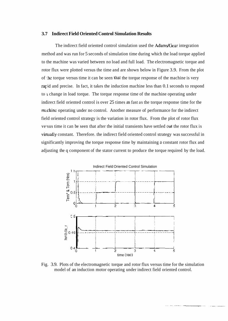
3.7 Indirect Field Oriented Control Simulation Results
The indirect field oriented control simulation used the AdamslGear integration
method and was run for 5 seconds of simulation time during which the load torque applied
to the machine was varied between no load and full load. The electromagnetic torque and
rotor flux were plotted versus the time and are shown below in Figure 3.9. From the plot
of l.he torque versus time it can be seen that the torque response of the machine is very
r a ~ i d and precise. In fact, it takes the induction machine less than 0.1 seconds to respond
to a change in load torque. The torque response time of the machine operating under
indirect field oriented control is over 25 times as fast as the torque response time for the
m;.chine operating under no control. Another measure of performance for the indirect
field oriented control strategy is the variation in rotor flux. From the plot of rotor flux
versus time it can be seen that after the initial transients have settled oul the rotor flux is
vir.tually constant. Therefore. the indirect field oriented control strategy was successful in
significantly improving the torque response time by maintaining a constant rotor flux and
adjusting the q component of the stator current to produce the torque required by the load.
Indirect Field Oriented Control Simulation
time (sec)
Fig. 3.9. Plots of the electromagnetic torque and rotor flux versus time for the simulation model of an induction motor operating under indirect field oriented control.

4. IMPLEMENTATION OF VOLTS PER HERTZ CONTROL
4.1 Implementation Overview
In a variable speed pulsewidth modulated induction motor drive system the
voltage applied to the motor must be varied in both frequency and magnitude. This task is
usually achieved through the use of a three phase voltage-source inverter. A single
mic:rocontroller can be employed to generate the sine wave modulated PINM drive signals
for the inverter as well as provide control functions for the drive system. This chapter
disc:usses the generation of sine modulated PWM drive signals and the digital
implementation of the volts per hertz control strategy on the Motorola NIC68F333
mic:rocontroller.
The Motorola MC68F333 ('333) is a modular microcontroller and is well suited
for AC motor control. The '333 is built around the CPU32 module, a 32-bit core processor
with an instruction set nearly identical to that of the MC68020. One new instruction,
Table Look-up and Interpolation (TBL), provides a means for linear interpolation between
points in a look-up table. In this research, the instruction is used to calculate the value of a
sin? wave from a relatively small number of entries. This instruction performs an 8-bit
table look-up and an 8-bit interpolation between consecutive entries. Therefore. 65,536
discrete values of the sine function can be represented by a look-up table (LUT)
containing only 256 entries.
Another module which is useful in the induction motor PWM drive system is the
Tirner Processor Unit (TPU) module. This module is a microcoded processor which
handles timing functions and can run semi-autonomously of the CPU32. One of the
microcoded timing functions, the Multichannel Pulsewidth Modulation (MCPWM)
function. uses externally gated multiple channels to generate sophisticated PWM drive
signals. These drive signals have a common period and independently varying pulse
widths, or high times. The function allows the user to select the timing relationship
between PWM drive signals as either center-aligned or edge-aligned. The MCPWM
function can also generate a periodic interrupt request for high time updating. The TBL
inslruction, MCPWM function and the microcontroller's ability to opera1.e at 16.777 MHz
are the primary features of the '333 which are critical in the generation of accurate PWM
drive signals.
The Queued Serial Module contains two serial interfaces, the queued serial
peripheral interface (QSPI) and the serial communications interface (SCI). In this
research project, the SCI is used to provide a means of serial communication between the
'333 and a personal computer (PC). The SCI is configured so that an inlerrupt request is
gerierated whenever data is transmitted from the PC to the '333 . The associated interrupt
service routine is programmed to implement the volts per hertz control strategy. This
module provides a means of motor control through a simple serial comu~unication
interface.
The source code written to generate the PWM drive signals and implement the
volts per hertz control strategy is stored in the 16-Kbyte flash EEPROM module of the
'333 microcontroller. The source code can be divided into three separate sections with the
lasl. two sections being interrupt driven. The first section is responsible for the
cordiguration of the various modules and the initialization of the program variables. The
second section is an interrupt service routine which is responsible for the calculation of the
new PWM drive signal high times. This routine is executed on a periodic basis. The third
section is an interrupt service routine which is responsible for implementing the volts per
hertz control strategy. This routine is executed only when the user comn~ands a change in
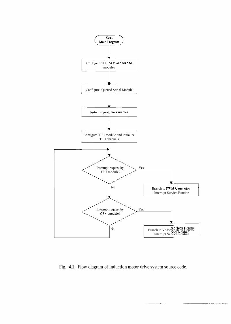
the speed of the machine. A flow diagram of the overall system is shown in Figure 4.1.
Th: code with edge-aligned PWM drive signals is shown in Appendix 1) while the code
wii h center-aligned PWM drive signals is shown in Appendix E.
4.2, Module Configuration and Parameter Initialization
The ' 333 microcontroller contains two different on-chip random access memory
(RAM) modules which need to be configured at the start of the program. The standby
Main Program :+; modules
Configure Queued Serial Module
Initialize program variables r Configure TPU module and initialize
TPU channels
Fig. 4.1. Flow diagram of induction motor drive system source code.
Interrupt request by Yes TPU module?
No Branch to PWhI Generahon Interrupt Service Routine
Interrupt request by Yes
No Branch to Volts per Hertz Control Interrupt Service 1 Routine
RAM module with TPU emulation capability (TPURAM) is a 3.5-Kbyte array of fast (two
bus cycle) static RAM. In emulation mode the TPU uses the TPURAM, normally used by
the CPU32 module, to store timing functions which are not stored in the microcode ROM
of the TPU module. Since the MCPWM function was not included in the microcode
ROlM of the TPU, the TPURAM must be used to store the function. After the source code
containing the MCPWM function has been assembled and loaded into the TPURAM the
TPU module must be put into emulation mode. When the TPU enters emulation mode,
the TPURAM is dedicated to the TPU and replaces the microcode ROM. Also the
TPLTRAM module is no longer accessible by the CPU32 module. Refer to [6], [7] and [8]
for more detailed information regarding the TPURAM module and emulation mode.
The standby RAM (SRAM) module is a 5 12-byte array of fast (two bus cycle)
static RAM. The SRAM module is configured so that the array occupies the first 512
by1.e~ of the processor memory map. This array is then used to store the program variables
and exception vector table. The exception vector table contains a total of 256 exception
vectors with 64 vectors defined by the processor and 192 vectors reserved for user
de Gnition. In this application, an exception vector was defined for each of the two
interrupt service routines. For further information regarding the SRAM module refer to
[6: and for further information regarding exception vectors refer to [9].
The third module which must be configured is the Queued Serial Module (QSM).
Tk,e Serial Communications Interface (SCI) of the QSM must be configured to transmit
and receive data at a rate of 9600 baud and generate an interrupt request whenever data is
received. An interrupt level and vector address must also be specified. ' h e interrupt level
determines the priority of the interrupt request while the interrupt vector address
corresponds to the appropriate vector in the exception vector table. For further
information regarding the configuration of the QSM refer to [6].
The program variables are initialized and the starting addresses of the interrupt
routines are written to the corresponding exception vector rollowing the configuration of
the memory modules and the QSM. The program variables along with their definitions
ar~d initial values are listed in Table 4.1. The user defined exception vectors along with
their associated interrupt service routine assignments are listed in Table 4.2. The reader
Table 4.1. Program variables, definitions and initial valu~es.
I V 1 Reference voltage 1 0 volts 1
Program Variable
-
f Reference frequency
I PER2 1 One-half PWM drive signal period 1 128 TPU clock cycles I
Variable Definition .-- --.
I TBLNUM / Previous position in look-up table 1 0 1
-v Initial Value
( b w 10)
I I
I First RPM digit to be displayed
P P --- -. =
Second RPM digit to be displayed
I - - 1 DIG3 1 Third RPM digit to be displayed 0 7
DIG4 1 Fourth RPM digit to be displayed I
Table 4.2. User defined exception vectors and associated vector assignments.
! voI'P1 i Points to the starting address of the PWM generation interrupt service routine.
Exception Vector Vector Assignment
-- -.-. 1
should note that the reference voltage, V, is scaled to a maximum value of 1024 to
accommodate integer multiplication and division. The reader should also note that the
va.riables PER and PER2 are specitied by the number of TPU clock cyc:les, where a TPU
cllnck cycle is approximately equal to 238 nsec. The reference voltage and frequency are
each initialized to zero in order to ensure that the motor starts from rest when the
processor comes out of reset.
The TPU module is the final module which requires configuration. An interrupt
level and vector address must first be assigned to the TPU module. The interrupt level
I
"":'- Points to the starting address of the volts per hertz control interrupt service
determines the priority of the interrupt request while the interrupt vector address
cori-esponds to the appropriate vector in the exception vector table. Nex~:, the MCPWM
funztion is selected for each of the active TPU channels. The number of active TPU
channels is dependent on the mode of operation for the MCPWM function. The MCPWM
function allows the user to select either edge-aligned or center-aligned timing
relationships between multiple PWM drive signals. A brief summary of the two modes of
ope ration is given in the following paragraphs. However, a complete performance
evaluation of the MCPWM function operating in each of the two modes is given in
Chapter 5. For further information regarding the MCPWM function refer to [lo].
In the edge-aligned mode, the PWM drive signals have aligned rising edges. The
edge-aligned mode requires four channels to generate three balanced PMTM drive signals.
The first TPU channel operates as the Master channel which is responsible for channel
syr~chronization and the generation of periodic interrupt requests. The next three TPU
channels operate as Slave channels. Each of the slave channels is exterrially gated with
the master channel through an XOR gate to produce the three PWM drive signals.
In the center-aligned mode, the PWM drive signals have center-aligned high times.
The center-aligned mode requires eight TPU channels to generate three balanced PWM
drive signals. The first TPU channel operates as a Master channel which is responsible for
channel synchronization. The next six TPU channels operate as slave channel pairs. The
fir,jt channel in each pair is referred to as a Slave A channel and the second channel in
each pair is referred to as a Slave B channel. Each of the slave channel pairs are externally
gated through an XOR gate to produce the three PWM drive signals. The last TPU
channel is configured as a Master channel and is responsible for the generation of periodic
inlerrupt requests.
Two parameters which must be configured and are common to each of the PWM
drwe signals regardless of the mode of operation are the period and the high time. The
period is common to all three signals and only needs to be written to the TPU module once
before the channels are initialized. This parameter is specified by the number of TPU
cl13ck cycles where a TPU clock cycle is equivalent to 238 nsec. A value of 256 TPU
clock cycles was chosen and corresponds to a PWM signal frequency of 16.384 kHz. The
initial value of the high time parameter for each of the three PWM drive signals is written
to the TPU module before the channels are initialized and is equal to one half of the signal
period. The reader should note that after the TPU channels have been inj tialized, the high
time for each of the signals is updated by the CPU32 through a periodic interrupt service
routine and varies independently of the other PWM drive signals.
The master channel responsible for generating the interrupt request is configured
to generate a request every third period of the PWM drive signal regardless of the mode of
operation. This allows the CPU32 time to write the new high times to the appropriate
TPLJ channels and allows the TPU time to recognize the new high times before another
intt:rrupt request is generated. After all of the TPU channels have been configured each of
the channels are initialized and the interrupt enable bit of the channel responsible for
generating the interrupt request is set. Once this occurs, the processor is configured and
the program releases control to the two interrupt service routines.
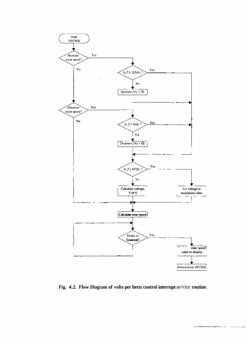
4.3 The Volts per Hertz Control Interrupt Service Routine
The volts per hertz control interrupt service routine (VFCISR) is responsible for
colltrolling the speed of the rotor by adjusting the reference frequency, j; and the relative
magnitude of the reference voltage, V, which in turn are used to control the frequency and
magnitude of the voltage applied to the machine. The user can comman~d a change in the
rotor speed through a simple serial communication interface between the host PC and the
'333 microcontroller. A command to increase the speed of the rotor is issued by the user
prf:ssing either the 'f' or 'F' key on the host PC keyboard. Likewise, a command to
decrease the rotor speed is issued by the user pressing either the 's' or '15' key on the
keyboard. An interrupt request is generated by the QSM whenever the user attempts to
transmit data to the '333 microcontroller. Once the CPU32 acknowledges and accepts the
inlerrupt request the VFCISR is executed. The flow diagram of the volts per hertz control
inierrupt service routine is shown below in Figure 4.2.
The first task of the VFCISR is to determine whether the user is issuing a
command to increase or decrease the speed of the rotor. If the user commands an increase
in the speed of the rotor, and the current reference frequency, f, is less than the maximum
VFCISR P
Yes
No Yes
S o
Decrease f by 1 HZ A
Calculate voltage, Si:t voltage to maximum value 1
Calculate rotor speed L,
Transmit?
rotor speed 1 value to display 1
Fig. 4.2. Flow Diagram of volts per hertz control interrupt senice routine.
frequency allowed, 120 Hz, then f is increased by 1 Hz and the new value: off is compared
to rated frequency of the machine, 60 Hz. If the new value off is less than the rated
frequency, then the new reference voltage, V, is calculated by multiplying f by the constant
k, where k is defined below in Equation (4.1).
Otherwise, the new value of V is set to its maximum value of 1024. If the user commands
an increase in the speed of the rotor, and the current reference frequency, f, is greater than
or equal to the maximum frequency allowed, then f remains unchanged m d Vis set to its
maximum value.
If the user commands a decrease in the speed of the rotor, and the current reference
frequency,f, is greater than the minimum frequency allowed, 0 Hz, then f is decreed by 1
Hz and the new value off is compared to rated frequency of the machine. If the new value
of f is less than the rated frequency, then the new reference voltage, V, is calculated by
multiplying f by the constant k, where k is defined in Equation (4.1). Otherwise, the new
value of V is set to its maximum value. If the user commands a decrease in the speed of
the rotor, and the current reference frequency, f, is equal to the minimurn frequency
allowed, then f remains unchanged and V is set to zero.
Once the new reference voltage and frequency values have been determined, the
rejerence speed is transmitted to the host PC where it is displayed. If the interrupt service
routine is executed by the user inadvertently pressing a key other than 'f'. 'F', 's' or 'S',
then the reference frequency and voltage are not changed and the calculated rotor speed
reinains the same.
4.4 The PWM Drive Signal Generation Interrupt Service Routine
The generation of classical sine-modulated PWM drive signals is accomplished by
comparing a sinusoidal reference waveform to that of a triangular carrier waveform.
When the magnitude of the reference waveform is greater than that of the carrier then the
output level of the PWM drive signal is high. However, in the discrete time domain this
approach is not feasible and an algorithm which can be implemented digitally must be
developed.
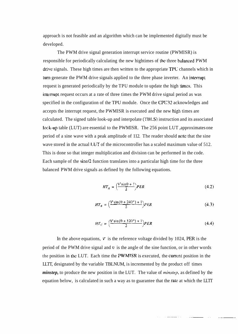
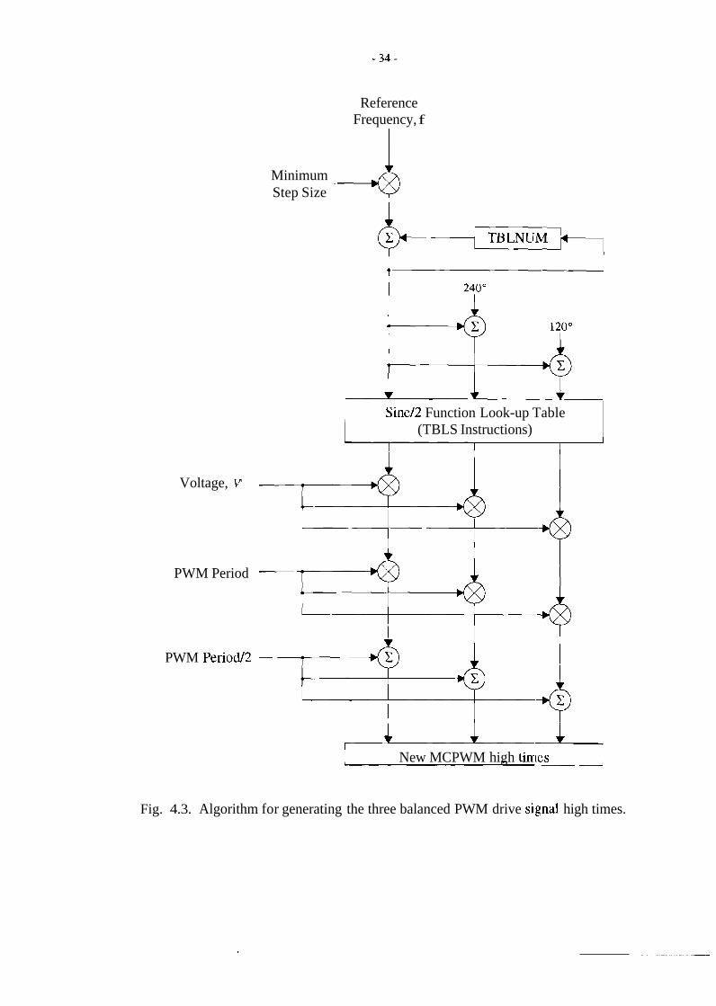
The PWM drive signal generation interrupt service routine (PWMISR) is
responsible for periodically calculating the new hightimes of the three balanced PWM
drive signals. These high times are then written to the appropriate TPU channels which in
tun1 generate the PWM drive signals applied to the three phase inverter. An interrupt
request is generated periodically by the TPU module to update the high rimes. This
int6:rmpt request occurs at a rate of three times the PWM drive signal period as was
specified in the configuration of the TPU module. Once the CPU32 acknowledges and
accepts the interrupt request, the PWMISR is executed and the new high1 times are
calculated. The signed table look-up and interpolate (TBLS) instruction and its associated
loclk-up table (LUT) are essential to the PWMISR. The 256 point LUT ,approximates one
period of a sine wave with a peak amplitude of 112. The reader should note that the sine
wave stored in the actual LUT of the microcontroller has a scaled maximum value of 512.
This is done so that integer multiplication and division can be performed in the code.
Each sample of the sine12 function translates into a particular high time for the three
balanced PWM drive signals as defined by the following equations.
In the above equations, v is the reference voltage divided by 1024, PER is the
period of the PWM drive signal and 0 is the angle of the sine function, or in other words
the position in the LUT. Each time the PWMTSR is executed, the cum:nt position in the
LLTT, designated by the variable TBLNUM, is incremented by the product off times
minstep, to produce the new position in the LUT. The value of minstep, as defined by the
equation below, is calculated in such a way as to guarantee that the ratt: at which the LLTT

is stepped through is equal to reference frequency,$
Therefore, the sine12 function will appear to have a frequency equal to that of the
reference frequency. After the new position in the LUT is determined, its value is copied
and shifted by the appropriate amounts to form a balanced set of sine12 functions. Once,
the three positions in the LUT are located, the values of the sine12 functilon can be
determined by using the TBLS instruction. The new high times are then calculated by
substituting the sine12 values into equations (4.2) through (4.4). Since the high times of
the three balanced PWM drive signals are calculated using the sine12 furrction, the
PU'MISK produces sine modulated PWM drive signals with the fundamental component
having a frequency equal to that of the reference frequency. The algorithm used in the
PM7MISR is shown in Figure 4.3. Refer to [ll] for further information regarding this
algorithm.
Reference Frequency, f
I
Voltage, v
PWM Period
PWM Period2
Minimum Step Size
SineM Function Look-up Table (TBLS Instructions)
1 New MCPWM high tirr~es I
Fig. 4.3. Algorithm for generating the three balanced PWM drive signal high times.
5. ANALYSIS OF PWM DRIVE SIGNALS
5.1 PWM Drive Signal Overview
In this chapter, the spectra of the edge-aligned and center-alignedl PWM drive
sigrlals generated by Motorola's MC68F333 microcontroller are analyze'd, evaluated, and
conlpared to that of the classical sine-modulated PWM drive signal. If the drive signals of
the A, B and C phase legs of the inverter are denoted PWM,, PWMB ancl PWMc and
assuming ideal switching, the line-to-line output voltage of the inverter rnay be derived
froin the following equation
Neglecting switching delays the drive signal PWMAB is a very close approximation to the
sha.pe of the line-to-line voltage actually applied to the induction machine and therefore
car1 be used to analyze and evaluate the harmonics delivered to the machine.
Two measures used to quantitatively compare the harmonic content of each signal
are the total harmonic distortion (THD) of the signal and the magnitude of the signal's
furtdamental component relative to the magnitude of the PWM drive signal itself. In this
paper, THD is defined by the following equation.
where the h subscript indicates the " h t h harmonic component of the signal. All evcn and
odd harmonics over the frequency spectrum of 0 Hz to 1800 Hz are used in the THD
calculation. Although significant harmonics are present around integer multiples of the
carrier frequency, 16.384 kHz, they are not included in the THD calculation because they
are located so much further out in the frequency spectrum. However, these harmonics are
shown and are taken into account during the evaluation of each signal generation scheme.
Each of the three PWM drive signals were analyzed at three different reference
frequencies, 30 Hz, 60 Hz and 90 Hz. These three frequencies were chosen so that the
siginals could be evaluated below, at and above the induction machine's rated excitation
frequency to provide some indication of variation over the speed range of the machine.
5.2 Classical Sine-modulated PWM Drive Signal Analysis
In a classical sine-modulated pulsewidth modulator, the PWM d ~ i v e signals are
generated by comparing a sinusoidal reference waveform to a triangular carrier waveform,
with the points common to both waveforms determining the edges of the PWM drive
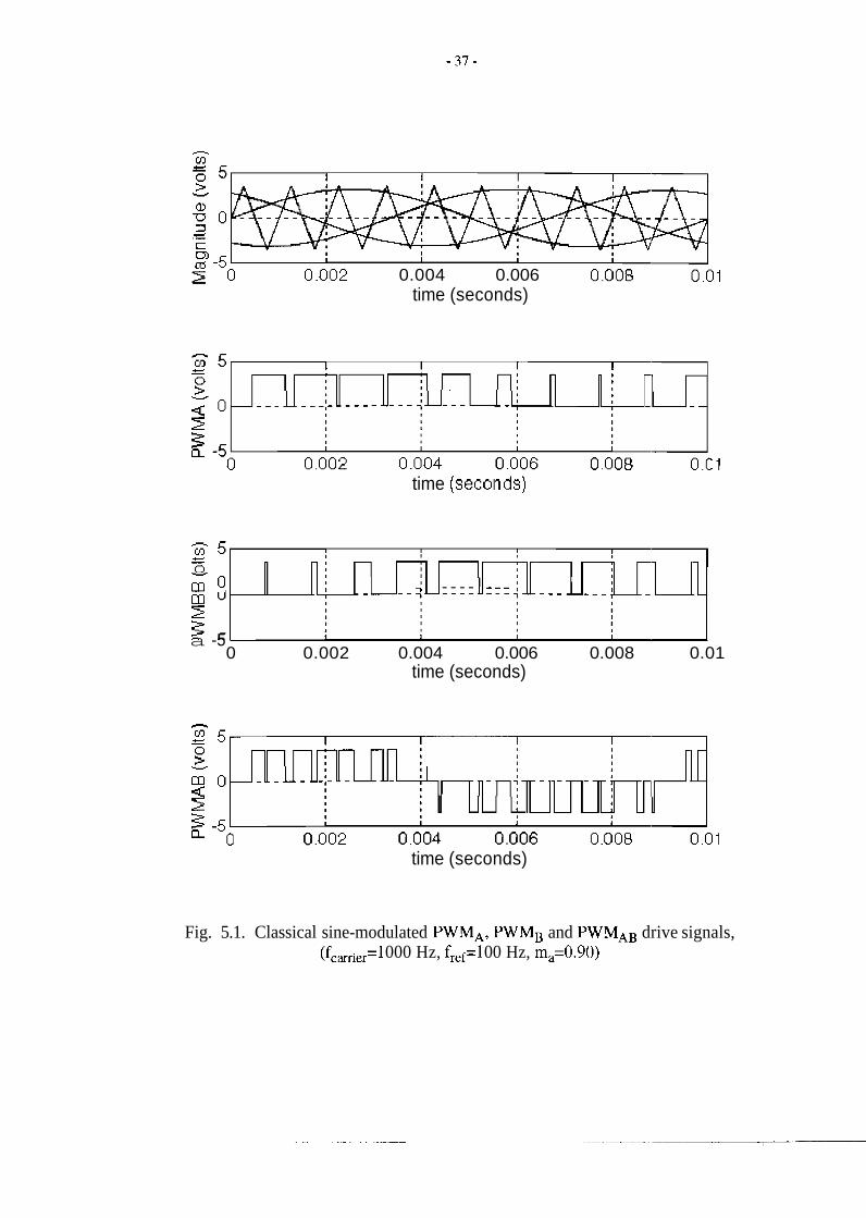
signals. Matlab was used to generate such a scheme and an example is shown in Figure
5.1. These signals, with a carrier frequency of 1000 Hz, a reference frequency of 100 Hz
andl an amplitude modulation index of 0.90, are used to illustrate the rel.ations between
each of the PWM signal pulses. It is clear from this figure that the c1ass:ical sine-
modulated PWM drive signals for each phase, PWMA and PWMB, have center-aligned
high times. The reader should note that these PWM signals are not be suitable for a
practical induction motor drive system because the carrier frequency ant1 the frequency
modulation index are much too low.
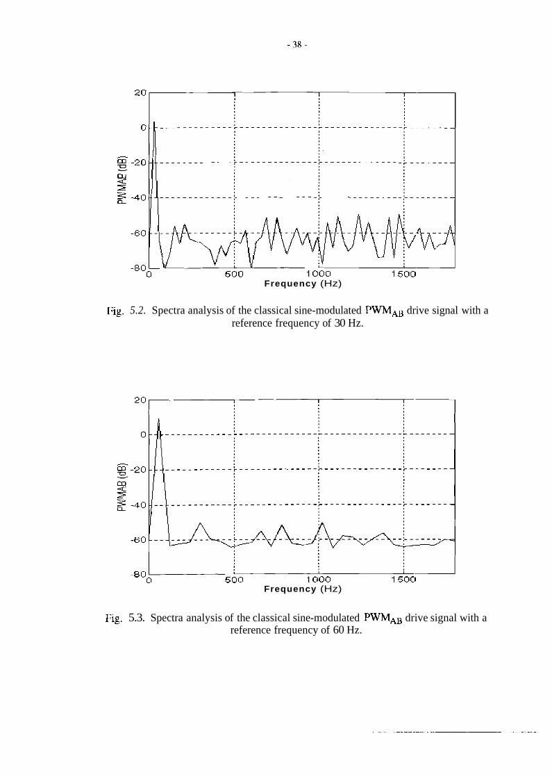
To analyze the harmonic content of the classical sine-modulated PWM drive
signal, the carrier frequency was increased to 16.384 kHz, which is equal to the carrier
frequency of the induction motor drive system. Matlab was then used to perform a Fast
Fourier Transform (FFT) on the drive signal, PWMAB, at reference frequencies of 30,60
andl 90 Hz. The amplitude modulation index was varied with the reference frequency to
ma:intain constant volts per hertz control. At a reference frequency of 30 Hz, the ma was
set to 0.5 and at reference frequencies of 60 and 90 Hz the ma was set to 1.0. The
fretjuency spectrum plots are shown in Figures 5.2 through 5.5. The THII and the relative
magnitude of the fundamental component at each reference frequency an: shown below in
0.004 0.006 time (seconds)
time (seco~ids)
> E 5 5 1 I U I V 1 J L _ 1 G ' o -I - - - - - - -
5 I I I
a -5 0 0.002 0.004 0.006 0.008 0.01
time (seconds)
time (seconds)
Fig. 5.1. Classical sine-modulated PWMA, PWMB and PWMAB drive signals, (fCxrier=1 000 Hz, fref=l 00 Hz, m,=0.90)
Frequency (Hz)
Fig. 5.2. Spectra analysis of the classical sine-modulated PWMAB drive signal with a reference frequency of 30 Hz.
Frequency (Hz)
Fig. 5.3. Spectra analysis of the classical sine-modulated PWMAB drive signal with a reference frequency of 60 Hz.
F3g. 5.4. Spectra analysis of the classical sine-modulated PWMAB drive signal with a reference frequency of 90 Hz.
5 10 15 Frequency (Hz) x lo4
Fig. 5.5. Spectra analysis of the classical sine-modulated PWMAB drive signal carrier harmonics with a reference frequency of 90 Hz.
Table 5.1. From the table it can be seen that when the reference frequency is set at 30 HZ
Table 5.1. Spectra analysis of the classical sine-modulated PWMd3 drive signal.
the THD is much greater than the THD at 60 Hz. and 90 Hz. This is simply due to the fact
that there are more harmonics present over the frequency band of 0 Hz to 1800 Hz for the
30 Hz signal than there are for the other two signals. It can also be seen that the relative
magnitude of the fundamental component at 30 Hz is much less than the relative
magnitude of the fundamental component at 60 Hz and 90 Hz. This is a direct result of the
reference voltage being decreased to half of its rated value to satisfy the volts per hertz
control condition.
The harmonics due to the carrier frequency are shown in the frequency spectrum
plclt of Figure 5.5. These harmonics occur at and around the integer multiples of the
carrier frequency. As the frequency increases the magnitude of the sidehands surrounding
each of these harmonics also increases. The magnitudes of these harmonics are much
greater than the magnitudes of the harmonics found over the frequency band used to
calculate the THD. However, since these harmonics occur at such high frequencies they
are easily filtered and do not greatly degrade the voltage applied to the machine. This
pal-ticular frequency spectrum plot was generated with the reference frequency set to 90
Hz,. Similar results were found at each of the lower frequencies as well. but for the sake
redundancy are left out of this paper.
5.91 Edge-aligned PWM Drive Signal Analysis
The multichannel PWM TPU function (MCPWM) of the MC68F333
microcontroller allows the user to select edge-aligned or center-aligned timing

relationships between multiple PWM drive signals. In the edge-aligned mode, the PWM
drive signals for each phase have aligned rising edges. The PWMA and PWMB drive
sigilals are constructed by externally gating the slave channel assigned to the signal with
the master channel of the MCPWM function through an XOR gate. A unity gain
difference amplifier is then used to construct the PWMAB drive signal. A schematic
diagram of the external circuitry used to generate the edge-aligned PWMk, PWMB and
Pfi'MAB drive signals is shown in Figure 5.6.
In the edge-aligned mode, the high times of the phase PWM drive signals are
updated every third PWM period. This allows enough time for the new high times to be
recl~gnized and used by the TPU module before the new high times are written, When a
new high time is written in edge-aligned mode and the write takes place before the falling
edge of the PWM drive signal, the new high time value is used in the n e ~ t period.
However, if the write takes place after the falling edge of the PWM drive signal, the new
high time value is not used until the second period after the write. Therefore, it is possible
that the high times of the phase PWM drive signals could be updated duiring different
periods. A high time update timing diagram where this occurs is shown in Figure 5.7.
This high time update uncertainty is unacceptable in a variable speed induction motor
drive PWM switching scheme.
Once the TPU interrupt request has been serviced, the CPU32 module requires 87
CPU clock cycles to respond and write the new high times for the three PWM drive
signals. Refer to [6] for a detailed analysis of instruction execution timiing calculations.
With a system clock frequency of 16.777 MHz, one CPU clock cycle is approximately
equal to 59.6 nsec. Therefore, if a drive signal has a current high time of less than 5.2
psec , which corresponds to a duty cycle of less than 8.5%, the new high time value for
that drive signal will not be used until the second period after the write. 'This results in the
incoherent updating of the high times for the three PWM drive signals.
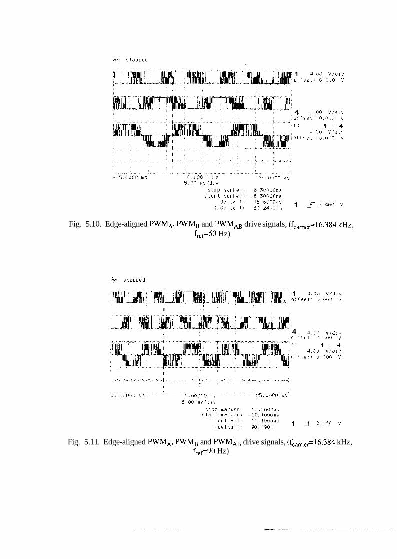
The PWMA, PWMB and PWMAB edge-aligned drive signals generated by the '333
mic:rocontroller are shown in Figures 5.8 through 5.11. In each of the figures, the top
waveform is the PWMA drive signal, the middle waveform is the PWMB drive signal and
Master lOkR PWMB
lOkR
lOkR
PWM A
lOkR
Fig. 5.6. External logic and subtraction circuit, edge-aligned mode.
k-- Per~od -4 I
I Master I
Channel I I
I I I I
Slave I I I I I I I I
Channel 1 I I I I
I I I I
1 I PWMA I
Slave I I
I I I
Channel 2 I I I I I I
PWMB I
(S2XOR MC)
Inltlaltzat~on of 1 P L l
channels
I PWM hlgh I PWM A high I PWM A high I ,tlmr rrcpgnlzrd I tme recognized I time used this I
I this prrtod I t h ~ s period I per~od I
I I I I I I I I PWM B high I I I I I tlme used this I
I I j period I I
i IRQ from New high
Master times Channel written by servlced CPU
IRQ from Master
Channel ser~lced
Fig. 5.7. High time update timing diagram, edge-aligned mode.
.:t.op marker: 5.680i)0111s s t.6r t. s a r k e r : - 4 . 32::Ii!rjms
Fig. 5.8. Edge-aligned PWMA, PWMB and PWMABdrive signals, (f,,,i,,=loOO Hz, fief= 100 HZ).
Fig. 5.9. Edge-aligned PWMA, PWMB and PWMAB drive signals, (fc,~e,=16.384 kHz, f , ,~30 Hz).
,..! ii:)i . ; . , . , J J s 75. i:11Qr]Q nc;
5 . 0 0 m s 7 d i v
s t o p h a r k e l - : 6 . S~iOuOni.; stnr! niar 'ker: -5.71?1:11;1!:1~!~
Fig. 5.10. Edge-aligned PWMA, PWMB and PWMAB drive signals, (fc,,~,,=16.384 kHz, f r , ~ 6 0 Hz)
I .. , .. I
4 4 , (31) '0, l' 13 : ' , j t . !
: ,j 1 " $, E t. ' I I , l . : l ~ I ~ ~ 5:
.. , I .. 0 . . . . .................................. f . .:..,... ..-... .. > ...... :.+..;. .: .. '...,.. :..i... .; ...... i . . . ..! ....... . . . . . . . . .- i..:. :...'..i I .
i .: , ,
. . . . . . . . . . . . . . . . . . . . . . . . . . . . i . . . . . . . . . . . . . . . . . . : r . . - . . . . . . . . . . . . . . . . . : . . . . . . . . . . . i ...:Ic - -, , !:J!;I~ I) nl 5 <I , (I !:! (11 [I CI 5 25. 01.;Cuj ir;
5.1jl j rfis:'dlv
,i,:cp m a r k e r : 1.301:100m5 5 t . a r t m a r k e r : -10, 10110ms
i l e l r n t : I I , I I > l ) ~ j l i i ~ 1 f 2.36i:l ' b i
I ! d e 1 t a I. : 91) . :?~I;I 1
Fig. 5.1 1. Edge-aligned PWMA, PWMB and PWMAB drive signals, (fc,,i,,=16.384 kHz, fref90 Hz)
SPECTRUM M a t h A: REF B: REF 0 M A R 30.001 Hz 20.00 0.000 v ~ a 3. $6252 o i3
i ~a 1 : ........ 1 N A G ............ + . ' I
. . ............ L . . . . . . .....
.......... ...... ......
..... ........ ...+. -.... ...... ....... ........
...... ........ ...- ... I
' .... ........ ,.... ..... ........ .....-..-.. '
.......
.... . . . .
.............. ...... -.
.. ........... ........... ........ i- ....
BTM 3IV START 0.001 Hz -80.00 10.00 S T O P 1 800.000 Hz RSW: 10 Hz ST: 6 . 8 6 m i n RANGE: 2- 0. T= O d B m
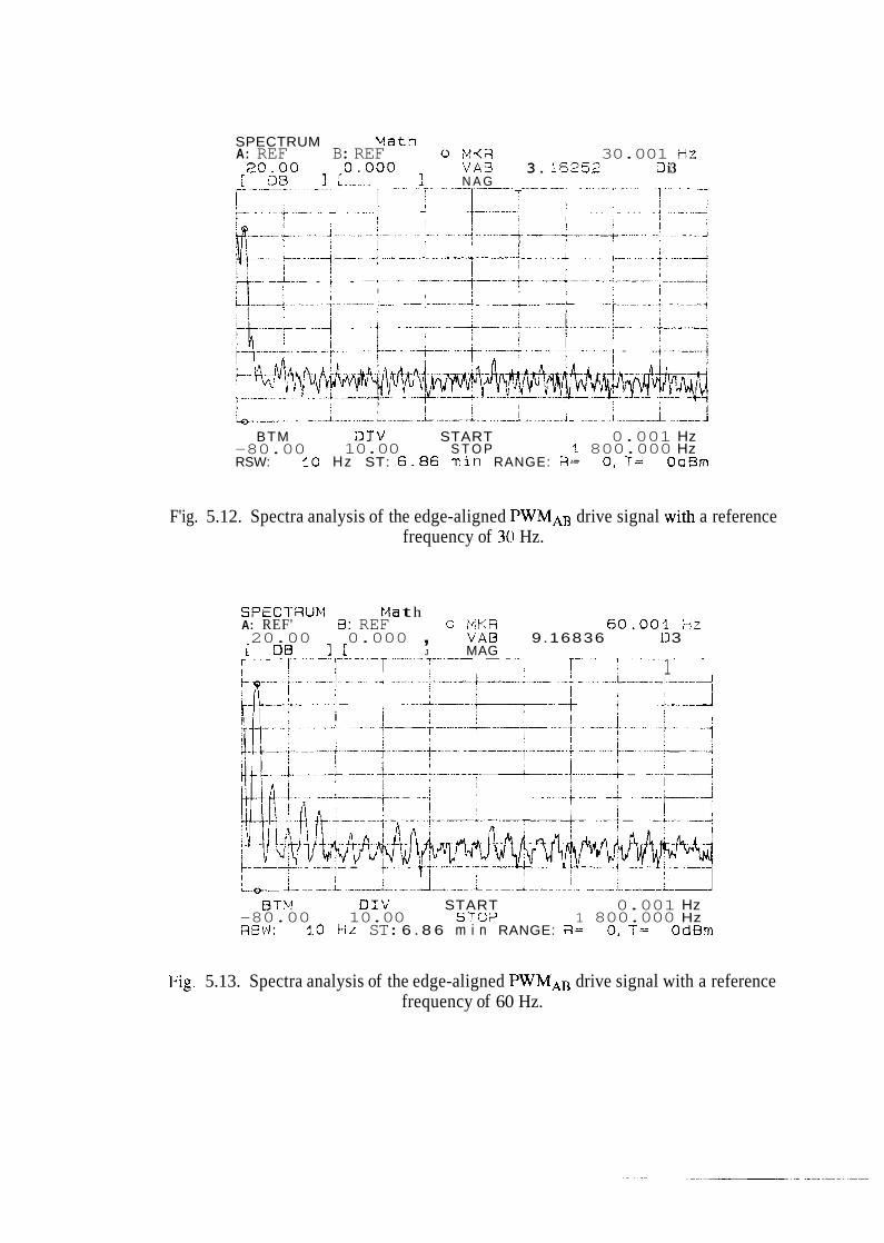
F'ig. 5.12. Spectra analysis of the edge-aligned PWMAB drive signal with a reference frequency of 30 Hz.
SPECTRUF.1 t4a t h A: REF' 9: REF 0 MKfi 60.00:l ? z 20.00 0.000 , \;At3 9.16836 11 3 [ Di3 j i J MAG ........... -----
....- ........ 1
L I
I .-i- .. ....
i ........ ..........
..........
....
. .-......... ......- .........
......
........
BTFl D I L ' START 0.001 Hz -80.00 10.00 STOF 1 800.000 Hz F1BW: 10 Hz ST: 6 . 8 6 m i n RANGE: R= 0. T- OdBm
Fig. 5.13. Spectra analysis of the edge-aligned PWMAB drive signal with a reference frequency of 60 Hz.
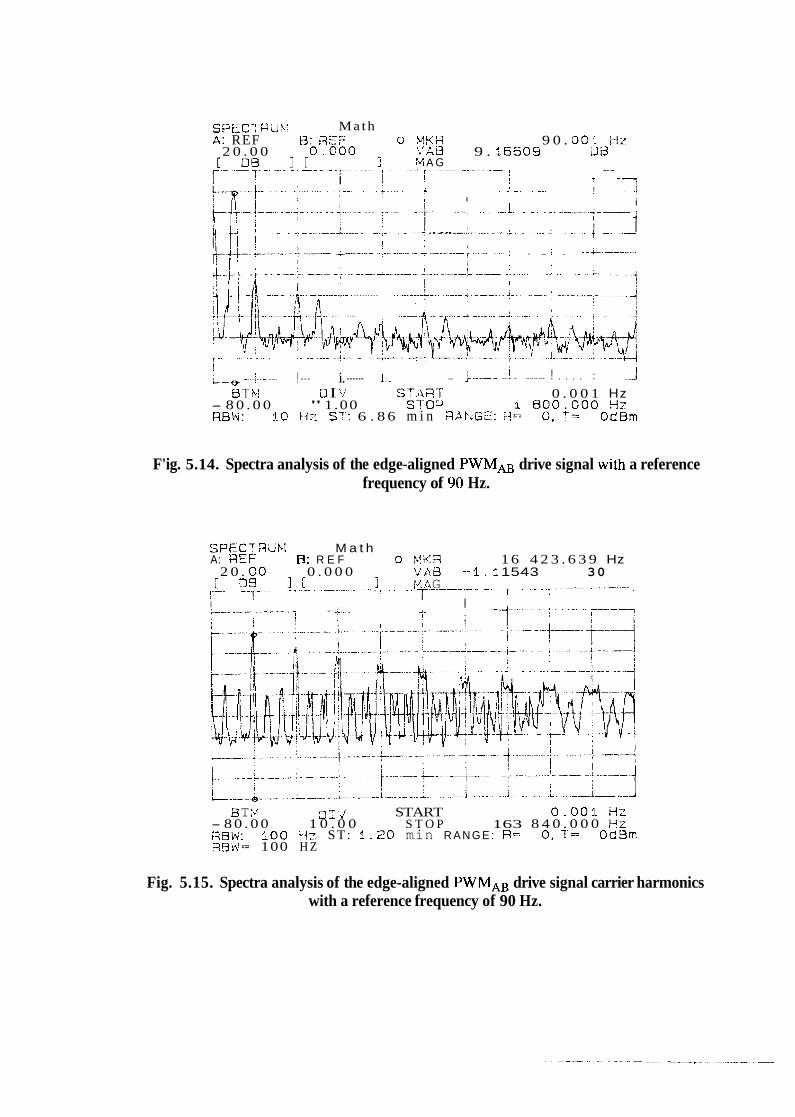
SPEC-;-^ J;%: M a t h A: REF 13: RSF- O MKS 9 0 . OCi: i - l ~
2 0 . 0 0 9 . i 6 6 0 9 2 i3 rvi A G !
i ! 4 j --j ... . . . . . . . ! ~ ~ 2
! I I i
.... ... .-. -~ --- ; . .... -.' ....... I i ! . . . . .... .: . . . . f -~ ...- i
! i . . . . . -- : : -:. - -C-------
... -I... I 4 --- .: ... . . . . . . ...' -- I
.........
....
. . . . . - . -. . . . - .... 1 --
1.
i ! . . . . ..... ...... ... i-, i ! i. ._.I._ i - L _ ! : __I
i3 7- b! i3 I '%i ST.a>T 0 . 0 0 1 Hz - 8 0 . 0 0 " 1.00 S7-03 1 t300.000 3-f~ HB!4: 10 t-lx ST: 6 . 8 6 m i n RAEJGE: 2- 0. T- OdBrn
F'ig. 5.14. Spectra analysis of the edge-aligned PWMAB drive signal .with a reference frequency of 90 Hz.
SPECT'RLJM M a t h A: FIEF 8: R E F 0 MKR 16 4 2 3 . 6 3 9 Hz
2 0 . C o 0 . 0 0 0 '+!AB --I. t 1543 30 [ DB I [ 1 14 A G ................... .-.-.---,-.- -. .. [ . . . . . . . ? - ........ . - . . . . . r-- I
I I I 1 . .. . . - . - - - . - $ . ~ . 2- ... 1 1 -
E3 T :%<I 3 1 ..,I START 0 . 0 0 ? . HZ - 8 0 . 0 0 1 0 . 0 0 S T O P 163 8 4 0 . 0 0 0 PZ RBW: i O O f i z ST: l. 20 min R A N G E : R- 0. 7'= OdBm 2BW= 100 H Z
Fig. 5.15. Spectra analysis of the edge-aligned PWMAB drive signal carrier harmonics with a reference frequency of 90 Hz.
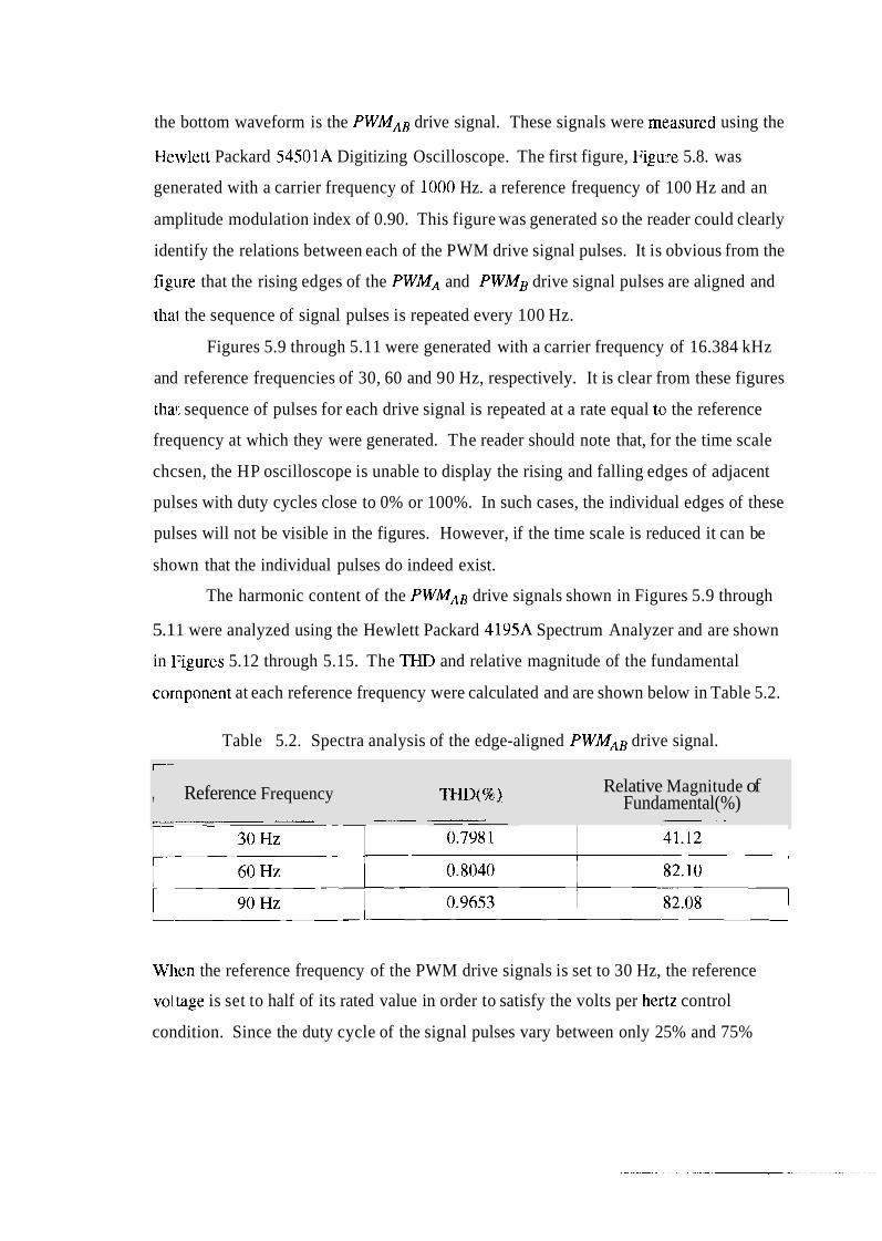
the bottom waveform is the PWMAB drive signal. These signals were me:asured using the
Hewlett Packard 54501A Digitizing Oscilloscope. The first figure, Figuire 5.8. was
generated with a carrier frequency of 1000 Hz. a reference frequency of 100 Hz and an
amplitude modulation index of 0.90. This figure was generated so the reader could clearly
identify the relations between each of the PWM drive signal pulses. It is obvious from the
figure that the rising edges of the PWMA and PWMB drive signal pulses are aligned and
that the sequence of signal pulses is repeated every 100 Hz.
Figures 5.9 through 5.11 were generated with a carrier frequency of 16.384 kHz
and reference frequencies of 30, 60 and 90 Hz, respectively. It is clear from these figures
thar. sequence of pulses for each drive signal is repeated at a rate equal ta the reference
frequency at which they were generated. The reader should note that, for the time scale
chcsen, the HP oscilloscope is unable to display the rising and falling edges of adjacent
pulses with duty cycles close to 0% or 100%. In such cases, the individual edges of these
pulses will not be visible in the figures. However, if the time scale is reduced it can be
shown that the individual pulses do indeed exist.
The harmonic content of the PWMAB drive signals shown in Figures 5.9 through
5.1 1 were analyzed using the Hewlett Packard 4195A Spectrum Analyzer and are shown
in Figures 5.12 through 5.15. The THD and relative magnitude of the fundamental
component at each reference frequency were calculated and are shown below in Table 5.2.
Table 5.2. Spectra analysis of the edge-aligned PWMAB drive signal.
When the reference frequency of the PWM drive signals is set to 30 Hz, the reference
vol.tage is set to half of its rated value in order to satisfy the volts per hertz control
condition. Since the duty cycle of the signal pulses vary between only 25% and 75%
r-
, Reference Frequency THD(%) Relative Magnitude of Fundamental(%)
--.- - - -. -- - . .
when the reference voltage is equal to half of its rated value, the CPU32 module has
enough time to coherently update the high times for all three PWM drivc: signal phases.
Thc: slight increase in the THD from the classical case can be attributed 1.0 the asymmetry
present in the drive signal. The asymmetry found in the signal is not uncommon in
practical PWM switching schemes. This asymmetry is a result of the fre:quency
modulation index not being equal to an odd integer multiple of three for all reference
frequency values. The even harmonics seen in Figure 5.12 verify that asymmetry is
indeed present in the PWMM drive signal when the reference frequency is set to 30 Hz.
When the reference frequency of the PWM drive signals is increased to 60 Hz, the
reference voltage is increased to its rated value to satisfy the volts per hertz condition and
the duty cycle of the signal pulses vary between 0% and 100%. Because the variation in
duty cycle has increased, the CPU32 module is unable to coherently update the high times
of I he drive signal phases on a consistent basis. This results in an increase in the harmonic
content of the PWMAB drive signal, and thus increases the THD despite the fact that the
number of harmonics present in the 60 Hz signal is less than the number of harmonics
present in the 30 Hz signal. The THD of the PWMAB drive signal increases further when
the reference frequency is increased to 90 Hz because fewer pulses are being used to
approximate a sinusoid at 90 Hz. Thus, the inability of the CPU32 module to coherently
upljate the signal high times on a consistent basis has a greater impact on the harmonic
content of the signal. The reader should note that the even harmonics seen in Figures 5.13
and 5.14 verify that asymmetry is also present in the PWM- drive signal when the
reikrence frequency is set to 60 and 90 Hz.
The harmonics of the carrier frequency in the edge-aligned PWh4M drive signal
arc: shown in the frequency spectrum plot of Figure 5.15. These harmollics are integer
m~iltiples of the carrier frequency and are of greater magnitude than the same harmonics
for the classical sine-modulated PWM drive signal. This increase in carrier harmonics is a
direct result of the decrease in the relative magnitude of the fundamental component of the
edge-aligned PWMAB drive signal. Although the carrier harmonics are not accounted for
in the THD calculation, they do decrease the efficiency of the signal. The energy lost in
lOkR
IOX-R
lOkR
Fig. 5.16. External logic and subtraction circuit, center-aligned mode.
the: fundamental component of the edge-aligned PWMAB drive signal is distributed over
the: higher harmonics. The particular frequency spectrum plot in Figure 5.15 was
generated with the reference frequency set to 90 Hz. Similar results were found at each of
thc: other reference frequencies as well, as such they are not shown in this thesis.
5.4 Center-aligned PWM Drive Signal Analysis
In the center-aligned mode, the PWM drive signals for each phase have center-
aligned high times. The PWMA and PWMB drive signals are construcled by externally
gating the slave A and slave B channels assigned to each signal through an XOR gate. A
urity gain difference amplifier is then used to construct the PWMAB drive signal. A
schematic diagram of the external circuitry used to generate the edge-aligned PWMA,
PWMB and PWMa drive signals is shown in Figure 5.16.
In the center-aligned mode, the high times of the phase PWM dnve signals are also
updated every third PWM period. This allows enough time for the next set of high times
to be recognized and used by the TPU module before the new high times are written.
U'hen a new high time is written in center-aligned mode and the write ~.akes place before
the rising edge of the PWM drive signal, the new high time value is used in the next
k- Period 4 Master
Channel I I
I I I I
P W M A { (A1 XORB1)
I I I I I
Slave Channel A1
Slave Channel A2
I I I
I I I
I I I
I I
Slave Channel B2
I I I I I I
Slave I I I
Channel B1 I I I I I I
PWM B (A2 XOR B2)
2nd Master Channel
I 1 I I 2nd Master Channel laps 1st DI rc New high t i m e s : ~ e w tugh times I
I I due to P1.7 service latencies I I I recognized this I used coherenlly I I
I I I I period I th~s period I I I / I I I I I I I I I I I I
i Initialization
of TPU channels
IRQ from Maximum 2nd Maqter timeavallable
Channel for CPU to serviced write new
high times
IRQ from 2nd Master
Channel serviced
Fig. 5.17. High time update timing diagram, center-aligned mode.
period. If the write takes place after the rising edge of the PWM drive signal, the new high
time value is not used until the second period after the write.
Coherent updating of PWM drive signal high times can be acconiplished in center-
aligned mode by using a second Master channel solely for periodic interrupt generation.
Thl: second Master channel runs at twice the speed of the Master channel. It is responsible
for PWM generation and is configured to request an interrupt during the second half of
every third PWM period, close to the mid-point but after the other MCPWM channels
have been serviced. Once the request has been accepted. the CPU32 module has the
remainder of the PWM period to update the high times of the PWM drivle signals before
the next rising edge, thus guaranteeing the coherent use of the high times during the
seclsnd PWM period after the write. A high time update timing diagram for the center-
aligned PWMA and PWMB drive signals is shown in Figure 5.17.
The worst-case delay (DI) from the mid-point of the PWM period to the time the
inte:rmpt is serviced can be closely estimated by adding together the worst case service
times (WCST) for each slave channel and the 2nd master channel. For three center-
aligned PWM drive signals the worst-case delay is estimated by the equation below.
DI = 3( WCSTSA) + 3(WCSTSB) + WCSTM2 = 214 CPU clocks (5.3)
With a system clock frequency of 16.777 MHz, one CPU clock cycle is approximately
equal to 60 nsec. Therefore, with a camer frequency of 16.384 kHz, the CPU32 module
has approximately 24.1 psec to respond and write the new high times, which is obviously
greater than the 5.2 psec required by the CPU32 module to complete the task.
The PWMA, PWMB and PWMm center-aligned drive signals generated by the
'333 microcontroller are shown in Figures 5.18 through 5.21. In each ot' the figures, the
top waveform is the PWMA drive signal, the middle waveform is the PU7MB drive signal
and the bottom waveform is the PWMAB drive signal. These signals were also measured
using the Hewlett Packard 54501A Digitizing Oscilloscope. The first figure, Figure 5.18,
was generated with a carrier frequency of 1000 Hz, a reference frequenc:~ of 100 Hz and
an amplitude modulation index of 0.90. This figure was generated so the reader could
clearly identify the relations between each of the PWM drive signal pulses. It is obvious
from the figure that the high times of the PWMA and PWMB drive signal pulses are center-
ali,gned and that the sequence of signal pulses is repeated every 100 Hz. It can also be
seen from the figure that the center-aligned PWM drive signals are nearly identical to the
cla.ssica1 sine-modulated PWM drive signals.
The drive signals shown in figures 5.19 through 5.21 were generated with a carrier
frequency of 16.384 kHz and reference frequencies of 30,60 and 90 Hz, respectively. It is
clear from these figures that the sequence of pulses for each of drive signal is repeated at a
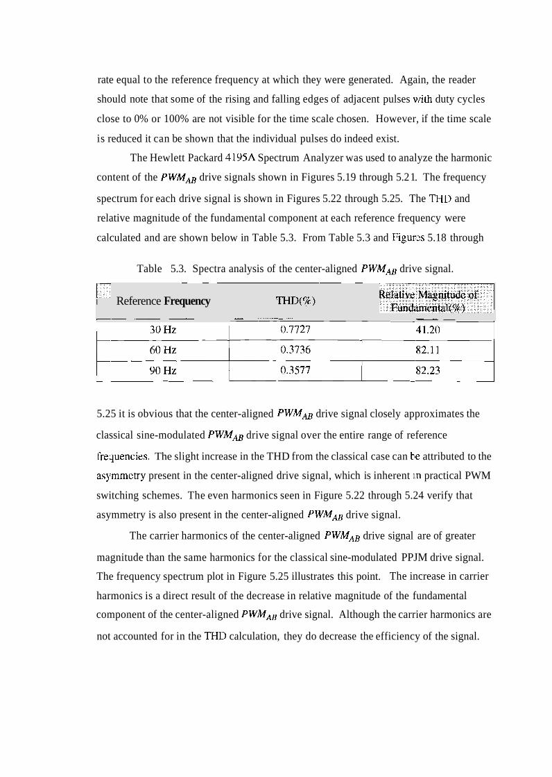
rate equal to the reference frequency at which they were generated. Again, the reader
should note that some of the rising and falling edges of adjacent pulses with duty cycles
close to 0% or 100% are not visible for the time scale chosen. However, if the time scale
is reduced it can be shown that the individual pulses do indeed exist.
The Hewlett Packard 4195A Spectrum Analyzer was used to analyze the harmonic
content of the P W M m drive signals shown in Figures 5.19 through 5.2 1. The frequency
spectrum for each drive signal is shown in Figures 5.22 through 5.25. The THD and
relative magnitude of the fundamental component at each reference frequency were
calculated and are shown below in Table 5.3. From Table 5.3 and Figurizs 5.18 through
Table 5.3. Spectra analysis of the center-aligned PWMm drive signal.
5.25 it is obvious that the center-aligned P W M m drive signal closely approximates the
classical sine-modulated P W M m drive signal over the entire range of reference
freyencies. The slight increase in the THD from the classical case can he attributed to the
asymmetry present in the center-aligned drive signal, which is inherent !In practical PWM
switching schemes. The even harmonics seen in Figure 5.22 through 5.24 verify that
asymmetry is also present in the center-aligned PWMm drive signal.
The carrier harmonics of the center-aligned PWM- drive signal are of greater
magnitude than the same harmonics for the classical sine-modulated PPJM drive signal.
The frequency spectrum plot in Figure 5.25 illustrates this point. The increase in carrier
harmonics is a direct result of the decrease in relative magnitude of the fundamental
component of the center-aligned PWMAB drive signal. Although the carrier harmonics are
not accounted for in the THD calculation, they do decrease the efficiency of the signal.
1- I Reference Frequency -- .- --
THD(%)
b - - . - ... --
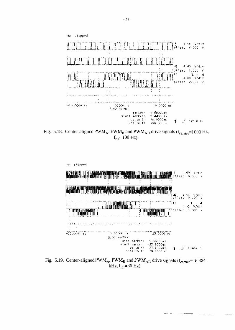
. " """" ...... " . . . " ....... .," .......... " ....... j7 1 I 5 n nlr-?r"! ! 4 . a o v ! o l v 1 J , 1 , I.,: i o f r s e t , ! ? . O I ~ Q ;: ..... . . . . . . . . . . . , .. .
A i
I .' I :
> : . . ;
.... 4 4 . r j 0 '~1 / ,j 1 %: 1 : I :
: I I : , I y ; . . .. ..-. ,.;. ; ...:..... . . . 7.. . . .......... :.. ...... :.....:.....;....,%..*...a. ... :.. ::
1 - 4
0 f i 5% ! : %,;I , !> b,:! 12 \;
. . .: ........... ' ....................... " .... ."I'.'"...'" ....... "' . . . ' . . . ..-......... " ....,.... ...... .'. ............. , . : I
I I : I
. . . . . . . . . . . . . . . . . . . . . . . . . . . . ...................... (..4 .:- ... :..: ........... ;.: ............. ..: .... :...;.. ...... * .:.. (... ................. .? . . . . . . .
: 1 : I
I i ...........,.... : . . . . . . . . . . . . . . . . . . . . . . . . . . . . . . . . . . . . . . . ........................ ...................... . . . . . . .
-7,). I : I I : :<I~, fils , i,:r?ijfii! :,: 1n:r,fi(~c0 n;: '7 ij [) 5 { fl 1 *y - .
ER,rl:er-: 7. ~~~I:II:I[I~~
s t ~ r t ~ Q r k s r : -:.140.:;i:ms j e i r a i. : 11:) , (I~JI:~~;I~~, 1 -f :34'5. i) p ? ~ '
1 :'jel t a t.: I~jlj.~ji;ilj 4:
Fig. 5.18. Center-aligncd PWMA. PWMB and PWMAB drive signals (f,,i,,=lOOO Hz, fref=lOO HZ).
i : o f f s e t : I ) (II:~(:I :i . . - . . . . . . . . . . . ....... .......... .................... ,.
f l
n i t , ; g f : ( ~ . f i ~ f i if
................... ...........-.. .......... . . . . . . . . . . . . . . . . . . . . . . . . , ' : -
I
. . . 1:. ' . . . . . . . . . . . . . . I . :..:,. i . . . . I. ; ..:.,: ........................ i : .. . .: r :. ......... .;.. .. ..: .-.: .: . . . . . : .... . .
. I :
,. . . . . . . . . . . . . . . . . . . . . . . . . . . . . . . . . . . . - . . . . . . . . . . 8.. ........... A . .......................... -2:. Ci<tfJ<! e s (i,[lI)OCICl 5 25 . I > I : I ~~ m q
5.00 n.-. 4 , 1 d 1 v ::top m a t h l i e r . 3,9l;01.:jds1s
s t a r t !itar;;er -2:.69013ms de! t a ! : 3 3 . 5 0 0 : 3 ~ ; 1 3- 2 , 0 6 3 ! j
: / d e l t a t : 2 3 . 5 5 0 7 L
Fig. 5.19. Center-aligned PWMA, PWMB and PWMAB drive signals; (fc,,,,=16.384 kHz, fr,f30 Hz).
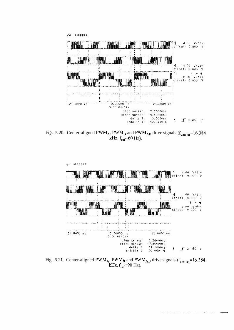
s t o p p e d
Fig. 5.20. Center-aligned PWMA, PWMB and PWMAB drive signals (fc,,er=16.384 kHz, fref=60 HZ).
I$p s t o p p e d
o f i s * : : 0.0iJO !i
1 - 4 ' 4 1;11:1 1; ,i 4 , s,,
o f f s e t . : ii.C101) \:
I I .. ! '
: I : . . . . . . . . i . . . . . . . . . . . I ......... .:. . : I . ../ : .:.:..: ...... :. . :....a. ; ... : .. :. ...... : ....... : .- ...... ;...... . : .... : ........ .; . . . . . . . . . . . . . . . . .
. I . : I : .j. , .
: . .............. i ............................. I ....... .; .............. :... ............................................. : . . . . :
- 2 5 , I) 0 0 I(, 5 0 . 030013 s 25. GO00 rs 5 . 1:4 n ~ s ? ' d i u
s!op mar -ker : 3 . :1)(100ms s t a r t m a r k e r : - 7 . Bt?rtOOn~.;
r f e l t e t : l l . !~ :100n.s 1 3- 2.469 'y' I t : 31:1.1!901 HZ
Fig. 5.21. Center-aligned PWMA, PWMB and PWMAB drive signals (fcarier=16.384 kHz, fref=90 HZ).
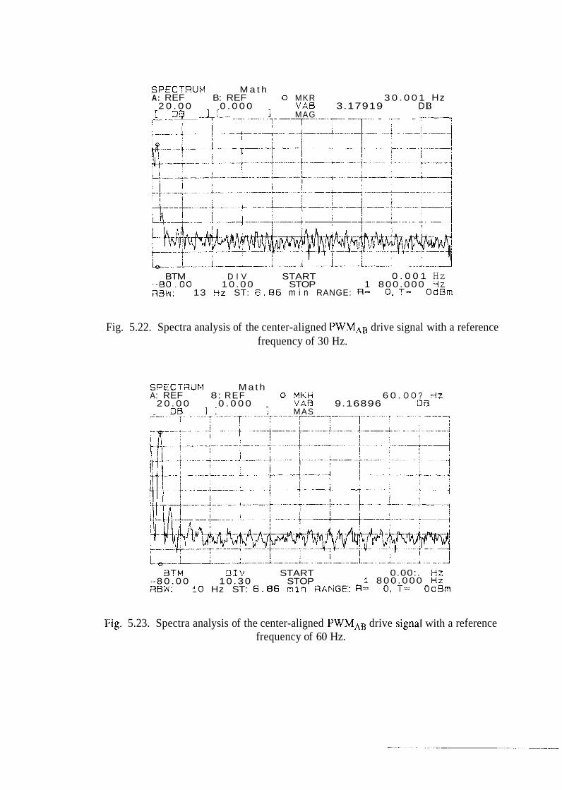
SPECTRUI.1 M a t h A: REF B: REF o MKR 3 0 . 0 0 1 Hz
2 0 . 0 0 0 . 0 0 0 V A B 3.17919 D I3 [ 33 , ---T-. I [ -. 1 MAG T- ....... ....... r..-7-.-. - .,.... - -7
BTM D I V START 0 . 0 0 1 Hz - 6 0 . 0 0 10 .00 STOP 1 800 .000 32 39~q: 13 g z ST: 6 . 8 6 m i n RANGE: R = 0. T= OdSm
Fig. 5.22. Spectra analysis of the center-aligned PWMAB drive signal with a reference frequency of 30 Hz.
SPECTFIUM M a t h A: REF 8: REF 0 MKR 6 0 . O O ? i?z
2 0 . 0 0 0 . 0 0 0 VAB 9.16896 OF3 DB j [ 2 MAS
BTM D I V START 0.00:. HZ --8 0 . 0 0 10 .30 STOP 2 800 .000 HZ RBW: L O Hz ST: 6.86 rnin FlkhiGE: R= 0. T= OdBm
Fig. 5.23. Spectra analysis of the center-aligned PWMAB drive signall with a reference frequency of 60 Hz.
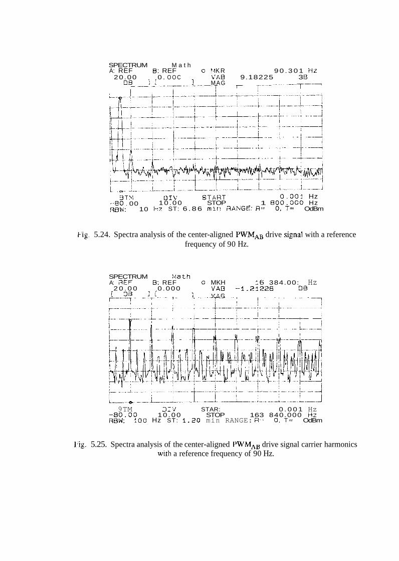
SPECTRUM M a t h A: REF B: REF 0 1.1 K R 9 0 . 3 0 1 i i z
20.00 0 . O O C V A B 9.18225 3 t3 DB : l 1 MAG .............. ?-- l--.--
I i : 7
3 T Y DIL' START 0 . 0 0 : Hz - -80 . 00 10 .00 STOP 1 600.OCCt Hz RBW: 10 i t z ST: 6 .86 m i r ! 3ANGE: A== 0. T= OdBm
F'ig. 5.24. Spectra analysis of the center-aligned PWMAB drive signa'l with a reference frequency of 90 Hz.
SPECTRUM Math A: FlEF B: REF 0 MKH 26 384.00: Hz
2 0 . 0 0 0 .000 brAR --1.21226 11 B [ 33 I [ r-.-T.- -. -. , . 1 .T....- ..... M A G . -. .. .,~ . . . . . . . . . . . . . . . . - > . .-
7 ! I i
9TM LIIV STAR: 0 . 0 0 1 Hz -80.00 10 .00 STOP 163 840.000 HZ RBW: $00 Hz ST: 1 . 2 0 min RANGE: 2.. 0. T= OdBm
Fig. 5.25. Spectra analysis of the center-aligned PWMAB drive signal carrier harmonics with a reference frequency of 90 Hz.
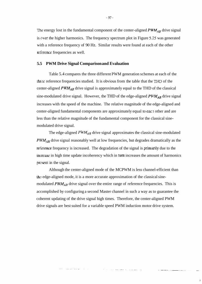
Tht! energy lost in the fundamental component of the center-aligned PWMM drive signal
is clver the higher harmonics. The frequency spectrum plot in Figure 5.2:5 was generated
with a reference frequency of 90 Hz. Similar results were found at each of the other
reference frequencies as well.
5.5 PWM Drive Signal Comparison and Evaluation
Table 5.4 compares the three different PWM generation schemes at each of the
thfi3e reference frequencies studied. It is obvious from the table that the THD of the
center-aligned PWMM drive signal is approximately equal to the THD of the classical
sine-modulated drive signal. However, the THD of the edge-aligned PMIMAB drive signal
increases with the speed of the machine. The relative magnitude of the edge-aligned and
center-aligned fundamental components are approximately equal to each other and are
less than the relative magnitude of the fundamental component for the classical sine-
modulated drive signal.
The edge-aligned PWMAB drive signal approximates the classical sine-modulated
PJVMAB drive signal reasonably well at low frequencies, but degrades dramatically as the
rejerence frequency is increased. The degradation of the signal is prim;uily due to the
increase in high time update incoherency which in turn increases the amount of harmonics
present in the signal.
Although the center-aligned mode of the MCPWM is less channel-efficient than
th,? edge-aligned mode, it is a more accurate approximation of the classical sine-
modulated PWMAB drive signal over the entire range of reference frequencies. This is
accomplished by configuring a second Master channel in such a way as to guarantee the
coherent updating of the drive signal high times. Therefore, the center-aligned PWM
drive signals are best suited for a variable speed PWM induction motor drive system.
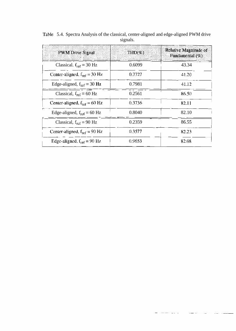
Table 5.4. Spectra Analysis of the classical, center-aligned and edge-aligned PWM drive signals.
1 Classical. fief = 30 Hz I 0.6099 43.34 I
Edge-aligned, fief = 30 Hz 0.7981
Classical, fief = 60 Hz 0.2561
Edge-aligned, fief = 60 Hz 0.8040 82.10
Classical, fief = 90 Hz 0.2359 86.55
6. CONCLUSIONS
6.1 Results
In this thesis, the performance of the volt3 per hertz and the field oriented control
str,itegies were evaluated through simulation. In Chapter 3, an implementation of the
vo Its per hertz control was successfully carried out with the soft-start feature limiting the
magnitude of the stator starting currents. When compared to the induct~on machine
opsrating under no control, the starting current was reduced by a factor of 3 and the
starting torque was correspondingly lowered by a factor of 7.
Likewise, it was shown through simulation that the indirect fieltl oriented control
was able to increase the torque response time of the induction machine while maintaining
a constant value of rotor flux. When compared to the machine operating under no control,
the indirect field oriented control strategy was able to increase the torque response time by
oker 2500%. Therefore, the indirect field oriented control strategy was also successful in
mzeting its objective.
A spectra analysis of the edge-aligned and center-aligned PWMAB drive signals
generated by the MC68F333 microcontroller operating under volts per hertz control were
p~esented in Chapter 5. From the spectra analysis. it was found that the edge-aligned
P WMAB drive signal closely approximatcd the classical sine-modulatetl PWMAB drive
signal at low frequencies, but degraded dramatically as the reference frequency was
increased. The degradation of the signal was primarily due to incoherent high time
updating which resulted in an increase in the harmonic content of the signal.
From the spectra analysis of the center-aligned PWMAB drive signal it was found
that this signal closely approximated the classical sine-modulated PWAdAB drive signal
over the entire range of reference frequencies. This was accomplished by configuring a

second master channel in such a way as to guarantee coherent updating of the drive signal
high times. Therefore, the center-aligned PWM drive signals are better suited for a
variable speed induction motor drive system despite the fact that the center-aligned mode
less channel efficient.
6.2 Future Work
The next phase of this research project would most likely include the incorporation
of the MC68F333 microcontroller into an actual induction motor drive system. This
would require interfacing the microcontroller with a three phase converier and modifying
the source code to include system protection. Further improvements coluld also be made
to the volts per hertz control interrupt service routine. Currently, the routine is operating
opm loop. However, the feedback loop could be closed by using the Quadrature Decode
(QDEC) function of the TPU module to measure the speed and position of the rotor. In a
sir2ilar manner, the stator currents could be measured to provide overcurrent protection.
Fllally, the volts per hertz control strategy could be replaced by field oriented control.
This would require the addition of the MC68882 floating-point coprocessor to handle the
trigonometric functions.
7. REFERENCES
J.A. Houldsworth and W.B. Rosink, "Introduction to PWM Speeld Control System for Three Phase a.c. motors," Electronic Components & Applicai5ons, Vol. 2, No. 2, February 1980.
R.M. Green and J.T. Boys, "Implementation of hlsewidth Modulated Inverter Modulation Strategies," IEEE Transactions on Industry Applica~~ions, Vol. IA-18, No. 2, pp. 138-145, MarchIApril 1982.
C. M. Ong, Dynamic Simulation of Electric Machinery, 1st ed., 1996, ch.9.
Ned Mohan, Tore M. Undeland, William P. Robins, Power Electronics, Converters, Applications, and design, 2nd cd., John Wiley & Sons, Inc., 1995, pp. 399-432.
Paul C. Krause, Oleg Wasynczuk, Scott D. Sudhoff, Analysis oj'Electric Machinery, McGraw Hill Book Company, 1986, ch. 3.
MCfi8F333 User's Manual, Motorola Inc., 1993.
TPU Tinzer Processor Unit Reference Manual, Motorola Inc., 1993.
Jeff Wright, Mike Pauwels, "Using the TPU Function Library and TPU Emulation Mode," Motorola Semiconductor Programming Note, Motorola. Inc., 1993.
CPU32 Reference Manual, Motorola Inc., 1993.
Jeff Wright, "Multichannel PWM TPU Function (MCPWM)," .Votorola Semiconductor Programming Note, Motorola Inc., 1993.
Jeff Baum and Ken Berringer, "Using the MC68332 Microconl.roller for AC Induction Motor Control," Motorola Semiconductor Application Note, Motorola Inc., 1993.

APPENDIX A: Block Diagrams of Induction Machine NIodel
Fig. A. 1. Induction machine block diagram.
Fig. A.2. abc2qds block diagram.
Fig. A.3. Q-axis block diagram.
Fig. A.4. D-axis block diagram.
U
p s k L.. -
- Tern-out
{g-m wrhb-cim
ids
Fig. A.5. Rotor block diagram.
ibs ids
Fig. A.6. qds2abc block diagram.

APPENDIX B: Induction Motor Equivalent Circuit Parameters
The stator resistance was determined by measuring the line-to-line resistance of
the machine when "cold7' and "hot" and then averaging the three measurements for each
case. The average resistance per phase was then calculated by dividing the line-to-line
resistance by two for each case.
19.8 + 19.8 + 19.7= 19.8R Ril , c o l d = -
3
21.1 + 21.1 + 20.9 R l ~ , h o t = 3 F 21.OR
- Rl l , hor - R p h , h o , - - - 10.5R 2
Since the Rph,hol is the more accurate measurement under loaded conditions this value was
used for the stator resistance.
Next, the no-load test was performed on the machine. This test corresponds to the
open-circuit test of a transformer. Therefore, under no-load conditions the circuit is
primarily reactive and the input impedance is approximately jxl , and jx, in series.

The third test performed was the block-rotor test. This test corresponds to the
short-circuit test of a transformer. Under blocked-rotor conditions the magnitude of the
impedance looking into the terminals of one phase of the machine was:
Assuming that the magnetizing impedance is much larger than the rotor
impedance, Zbr is defined as follows:
During the blocked rotor test, the rotor shaft cannot turn, thus w, = o and s = 1 .
Therefore, Rbr simplifies to
pt,, R,, = r, + r', = 7- z 15.84ST
31,r (B. 10)
from which the referred rotor resistance is
r', = R,,- r, z 5.34n (B.11)
The phase angle between the stator current and voltage during the blocked rotor test was
calculated as shown below.
%,, = acos - 32.37" [ h ; ; j b ]
(B. 12)
The imaginary part of Zhr can be calculated by substituting Equation (B. 12) into the
following equation.

X,, = IZ,,I sine,, z 10.04R (B.13)
For a Design B type motor, the stator and referred rotor reactances are:
The magnetizing reactance can be calculated by substituting Equation (B. 14) into
Equation (B.7) as shown below.
x, = IZ,,I - x,, E 124.22R (B.16)
The equivalent circuit with the machine parameters calculated above is shown in Figure
B. 1 below.
Fig. B. 1 The per phase equivalent circuit of a singly excited induction machine.


APPENDIX C: Induction Motor Full Load Operating Characteristics
The induction machine being studied throughout this research has been the
MagneTek Century AC Motor. The nameplate data from the motor was used to calculate
the stator excitation frequency, output power, and mechanical rotor speed of the machine
when operating under rated conditions, as shown below in Equations (C. 1) through (C.3).
rad = ( 6 0 H z ) ( 2 x r a d ) z 377-
S (C.1)
Pout,, = (;HP)(746%) = 186.5 Watts
rad - ( 1 7 2 5 ? ) ( 2 ~ ~ 9 ( ~ ~ ) E 180.64- O r m , f l - mzn rev 60 s s
The above calculations were then used to calculate electromechanical torque, slip speed,
slip frequency, and slip of the machine when operating under rated conditions, as shown
below in Equations (3.4) through (3.7).
rad O,,,,,, = a,,- (@r,n.ll. 1 5 . 7 2 ~

APPENDIX D: Center-aligned Source Code
..................................................................................... * MC68332 AC INDUCTION MOTOR THREE PHASE SINEWAVE GERERATION PROGRAM * ....................................................................................... * This program generates edge-aligned PWM signals for a three-phase inverter module which in turn * can drive an AC induction machine. The program enlploys open-loop, constant V/f control. The source * code was derived from a program created by Jeff Baum of Motorola, Inc.
*SCIM Registers SYNCR EQU SFFFA04 SYPCR EQU $FFFA20
*SRAM Module Registers SRAMMCR EQU $FFFB40 SRAMBAH EQU $FFFB44 SRAMB AL EQU SFFFB46
*TPURAM Module Registers TRAMMCR EQU $FFFB 00 TRAMBAR EQU $FFFB04
*TPU module registers TMCR TICR CIER CFSRO CFSRl CFSR2 CFSR3 HSQRO HSQR 1 HSRRO HSRRl CPRO CPRl CISR LR SGLR DCNR
* QSM/SCI control registers QMCR EQU $FFFCOO QILVR EQU $FFFCO4 SCCRO EQU SFFFC08 SCCR 1 EQU $FFFCOA
SCSR SCDR
* TPIJ parameter registers * TPUO: MCPWM Master Channel used for PWM alignment PERIOD-0 EQU $FFFFOO IRQ-PERIOD-0 EQU $FFFFO2 LAST-RT-0 EQU $FmTF04 LAST-FT-0 EQU $FFFFO6 RT-PTR-0 EQU $FFFFOS FT-PTR-0 EQU $FFFFO A
*TPUl: MCPWM Slave Channel (Phase a) - Edge-Aligned Mode PERIOD-1 EQU $FFFF 1 0 HIGHTIME- 1 EQU $FFFF 1 2 HT-PTR- 1 EQU $FFFF 1 6 RT-PTR_ I EQU $FFFF 1 8 FT-PTR- I EQU $FFFF I A
*TPU2: MCPWM Slave Channel (Phase b) - Edge-Aligned Mode PERIOD-2 EQU $FFFF20 HIGHTIME-2 EQU $FFFF22 HT-PI'R-2 EQIJ $FFFF26 RT-PTR-2 EQU $FFFF28 FT-PTR-2 EQU $FFFF2A
*TPU3: MCPWM Slave Channel (Phase c) - Edge-Aligned Mode PERIOD-3 EQU $FFFF30 HIGHTIME3 EQU SFFFF32 HT-PTR-3 EQU SFFI;F36 RT-PTR-3 EQU $FFFF38 FT-PTR-3 EQU $FFFF3A
* ISR-interrupt service routine location vectors VOFFl EQU $000 100 ;PWM ISR vector VOFF2 EQU $000 140 ;VFC ISR vector
* Main program labels v EQU F EQU PER EQU PER2 EQU TBLNUM EQU DIG 1 EQU DIG2 EQU DIG3 EQU DIG4 EQU
$000 180 ;reference voltage $000 1 82 ;reference frequency $000 1 84 ;pwm period $000 186 ;one-half pwm period $0001 88 ;position in look-up table $000 190 ;storage for SCI RPM digits $000 192 ;to display $000 19 4 $000 196
* MAIN PROGRAM
BEGIN ORG $10000
M0VE.W #$0000,TRAMMCR.L ;configure TPURAM for normal operation M0VE.W #$0000,TRAMBAR.L ;set TPURAM base address to $0000
Load the TPURAM Mask Set G Time Functions via ICD32
M0VE.W #$04CF,TMCR.L ;enable TPURAM M0VE.W #SOOOO,SRAMBAH.L ;configure SRAM for normal operation M0VE.W #$0000,SRAMMCRL ;set TPURAM base address to $0000
M0VE.W #$7FOO,SYNCR.L ;set system clock frequency to 16.777 MHz M0VE.W #$0000,SYPCR.L ;disable watchdog timer MOVE. W #$2400,SR ;supervisor mode, int mask 0
M0VE.L #$1 lOO0,VOFFl .L ;load PWMISR vector starting address M0VE.L #$11800,VOFF2.L ;load VFCISR vector starting address
BSR SCI-CNFG ;configure SCI
M0VE.L #$12000,AO ;load starting address of look-up table MOVE. W #$0400,V.L ;initialize voltage M0VE.W #$OOSA,F.L ;initialize frequency MOVE. W #$0000,TBLNUM.L ;initialize position in look-up table M0VE.W #$0 100,PER.L ;initialize pwm period
BSR TPU-CNFG ;configure and initialize TPU channels
BRA *
..................................................................................... *TPU configuration subroutine
TPU-CNFG M0VE.W #$0000,CPRO.L ;disables channels 8-1 5 M0VE.W #$0000,CPRl .L ;disables channels 0-7 MOVE.W #$OOCF,TMCR.L ;div4 clock, T2CG, IARB is F M0VE.W #$0640,TICR.L ;TPU intlvl 6, vector base $40 MOVE. W #$0007,CFSR2.L ;TP4: MCPWM M0VE.W #$7777,CFSR3.L ;TPO,TP 1 ,TP2,TP3: MCPWM M0VE.W #SOOOO,HSQR 1 .L ;slave channel type selection
TPUO RAM: Master MCPWM timing channel configuration M0VE.W #$0 100,PERIOD-0.L ;pwm frequency = 16.384 kHz M0VE.W #$0300,IRQ-PERIOD-0.L;request interrupt every period M0VE.W #$0004,RT-PTR-0.L ;last risetime address - master ch. M0VE.W #$0006,ET-PTR0.L ;last falltime address - master ch.
TPUl RAM: MCPWM Slave Channel configuration (Phase a) MOVE. W #$0100,PERIOD-l.L ;pwm frequency = 16.384 kHz M0VE.W #$0080,HIGHTIME-l.L ;initialize pwm duty cycle to 50% M0VE.W #$00 12,HT-PTRl .L ;hightime address - slave channel M0VE.W #$0004,RT-PTR-l.L ;last risetime address - master ch. MOVE. W #$0006,FT-PTR-l.L ;last falltime address - master ch.
TPU2 RAM: MCPWM Slave Channel configuration (Phase b) M0VE.W #$0 100,PERIOD-2.L ;pwm frequency = 16.384 kHz M0VE.W #$0080,HIGHTIME-2.L ;initialize pwm duty cycle to 50% M0VE.W #$0022,HT-PTR-2.1, ;hightime address - slave channel MOVE. W #S0004,RT-PTR-2.L ;last risetime address - master ch. M0VE.W #S0006,FT-PTR-2.L ;last falltime address - master ch.
TPU3 RAM: MCPWM Slave Channel configuration (Phase c) M0VE.W #$OlOO,PERIOD-3.L ;pwm frequency = 16.384 kHz M0VE.W #$0080,HIGHTIME-3.L ;initialize pwm duty cycle to 50% M0VE.W #$0032,HT-PTR-3.L ;hightime address - slave channel M0VE.W #$0004,RT-PTR-3.L :last risetime address - master ch. M0VE.W #$0006,FT-PTR-3.L ;last falltime address - master ch.
TPU Initialization MOVE. W #$03AB,HSRRl.L ;channel initialization 0RI.W #SO00 1 ,CIER.L ;enable TPO interrupt M0VE.W #$03FF,CPR1 .L ;channel priority RTS
......................................................................................... *SCI configuration subroutine
SCI-CNFGM0VE.W #$008 1 ,QMCR.L ;sup mode, iarb 1 M0VE.W #$0550,QILVR.L ;intlvl 5, vector $50 MOVE. W #S0037,SCCRO.L ;9600 baud M0VE.W #$002C,SCCR 1 .L ;RE, TE, RE RTS
*PWM interrupt service routine
PWMISR ORG $1 1000 AND1.W #$FFFE,CER.L ;disable TPO interrupt MOVE. W CISR.L,DO ;read interrupt status register AND1.W #$FFFE,CISR.L ;clear TE'O interrupt status bit
M0VE.W D 1 ,HIGHTIME- 1 .L ;write new high times to all M0VE.W D2,HIGHTIME-2.L ;three PWM phases MOVE. W D3,HIGHTIME-3 .L
M0VE.W PER.L,PER2 .L ;PER12 and store in PER2 LSR.W PER2.L
M0VE.W TBLNUM.L,D 1 ;load prev. TBLNUM in D l MOVE. W F.L,D2 ;put reference frequency in D2 MULU. W #$OC,D2 ;mult. freq. by 4 (min. step) ADD.W D2,D 1 ;add delta TBLNUM to old M0VE.W D 1 .TBLNUM.L ; save new TBLNUM
M0VE.W D 1 ,D2 ;copy f*t product to D2
ADD .W #$AAAA,D2 M0VE.W Dl,D3 ADD. W #$5555,D3
TBLS .W (AO),D 1 TBLS.W (AO),D2 TBLS .W (AO),D3
MULS.W PER.L,D 1 MULS.W PER.L,D2 MULS. W PER.L,D3
;add +240 deg. phase shift ;copy f*t product to D:3 ;add +I20 deg. phase shift
;look up sin(f*t)l2 value in table ;look up sin(f*t + 240)12 value ;look up sin(f*t + 120)/2 value
;multiply sine samples by V
;multiply sine samples by PER
ADD.W PER2.L,D 1 ;add period12 to all three phases ADD.W PER2.L,D2 ;for new pulse width calculations ADD.W PER2.L.D3
0RI.W #$000 1 ,CIER.L ;enable TPO interrupt RTE ;return from interrupt
*QSMISCI ISR-intermpt service routine
VFCISR ORG M0VE.W M0VE.W CMP1.B BEQ CMP1.B BEQ CMP1.B BEQ CMP1.B
$11800 SCSR.L,D7 SCDR.L,D4 #$46,D4 INCRPM #S66,D4 INCRPM #$53,D4 DECRPM #$73,D4
;read SCS R ;receive character ;check for 'F'aster
;check for 'f'aster
;check for 'S'lower
;check for 's 'lower
BEQ BRA
DECRPM ENDSVC ;illegal character, no changes
CMP1.W BGE ADDQ.W BRA
#$78,F.L COMPVOLT #$I ,F.L COMPVOLT
;do not exceed 120 Hz ;compute voltage ;increment freq. by 1 Hz ;compute voltage
INCRPM
DIZRPM
COMPVOLT
#$O,F.L COMPVOLT #$1 ,F.L
CMP1.W BLE SUBQ.W
;do not go negative in freq ;compute voltage ;decrement freq. by 1 132
CMP1.W BGE M0VE.W MULU. W M0VE.W BRA
#$3C,F.L CONSTVOLT F.L,D5 #$ll,DS D5,V.L ENDSVC
;check if >= 60 Hz ;maintain maximum v'dtage
;volts=freq* 17 ;store new voltage ;go calculate rpm's
CONSTVOLT
ENDSVC ;rpm=30*frequency
;poll bit 8 ti1 clear, ready to XMIT
;output <CR> to screen
;refresh digits to blank characters
BTST BEQ M0VE.W
;point to addr. to store: digits M0VE.L ADDQ .L
D1VU.W M0VE.W SWAP ADD1.B M0VE.W CLR.L MOVE. W CMP1.W BNE LEA MOVE.W#3,D7 BTST BEQ M0VE.W DBF RTE
#$A,DS D5,D6 D5 #$30,D5 D5,-(Al) D5 D6,D5 #$O,D5 BCDCONV DIGl.L,Al
;divide rpm hex by 10 ;copy D5low (quotient) to D6 ;put D5up (remainder) in D5 low :add $30 to convert tc ASCII
;clear entire D5 ;restore previous quotient to D5 ;check D5=zero, done converting ;loop to next conversion ;point to first digit to transmit ;reset transmit digit cwnter ;poll transmit complete flag
;write SCDR to transmit digit ;transmit next digit
*LOOK-UP TABLE (LUT) PWTRL ORG $12000
D W $0000,$000d,SOO 1 9,$0026,$0032,$003f,$004b,$0058 DW $006~,$oo70,$Oo7c,$0089,$0095,$00al,$00ac,$00b8 DW $00c4,$00cf,$00db,$00e6,S00f 1 ,$0Ofc,$0107,$0 1 12 D W $01 lc,$0127,$013 1,$013b,$0145,$014e,$0158,$0161 DW $016a,$0173,$017b,~0184,$018c,$0194,$019b,$01a3 D W $01aa,$01b1,$0lb7,$0lbd,$Olc4,$01c9,$01cf,$01d4 DW $01d9,$0lde,$Ole2,SOle6,$0lea,$01ed,$01f1,$01f4 DW SO1f6,$01f8,$01fa,$O1fc,$O1fe,$O1ff,S01ff,$0200 D W $0200,$0200,$01ff,$O1 ff,$O lfe,$01fc,$01fa,$01 f8 DW $Olf6,$01f4,$01f l,$O led,$Ol ea,$0 le6,$01e2,$0lde DW $01 d9,$01d4,S01 cf,$Olc9,SOlc4,$0 lbd,$0lb7,$0lbl DW $01aa,$01a3,$019b,$0194,$018c,S0184,$017b,$0173 D W S016a,$0161,$0158,$014e,$0145,$013b,$0131,$0127 DW $01 lc,$0112,$0 107,$00fc,$OOf 1,$00e6,$00db,$00cf DW $00c4,$C~0b8,$00ac,$OOal,$0095,$0089,$007~,$0070 DW $0064,$00~8,$004b,$003f,$0032,$0026,$0019,$~0d DW $0000,$fff3,$ffe7,$ffda,Sffce,Sffcl ,$ffb5,$ffa8 Dw $ffgc,$ffgO,$ff84,$ff77,$ff6b,$ff5f,$ff54,$ff48 DW $ff3c,$ff31 ,$ff25,$ffl a,$ffOf,$ffO4,$fef9,$feee DW Sfe&,$fed9,$fecf,$fec5,$febb,$feb2,Sfea8,$fe9f DW $fe96,$fe8d,$fe85,$fe7c,$fe74,$fe6c,$fe65,$fe5d DW $fe56,$fe4f,$fe49,$fe43,$fe3c,$fe37,$fe3l,$fe2~ DW $fe27,$fe22,$fel e,$fel a,Sfel6,Sfel3,$feOf,$feOc DW $feOa,Sfe08,Sfe06,$feO4,$fe02,$feOl,$fe01 ,$fe00 DW SfeOO,$feOO,$feO 1 ,$feOl ,$fe02,$fe04,$fe06,$fe08 DW $feOa,$feOc,$feOf,$fe13,$fel6,$fel a,$fele,$fe22 Dw $fe27,$fe2c,$fe3 l,$fe37,$fe3c,$fe43,$fe49,$f&f DW $fe56,$fe5d,$fe65,$fe6c,$fe74,$fe7c,$fe85,Sfe8d D W $fe96,$fe9f,$fea8,$feb2,$febb,$fecS,$fecf,$fed9 DW Sfee4,$feee,$fef9,$ff04,SffOf,$ff 1 a,$ff25,$ff3 1 DW $ff3c,$ff48,$ff54,$ff5f.$ff6b,$ff77,$ff84,$ff90 DW $ff9c,$ffa8,$fR&$ffcl,$ffce,$ffda,$ffe7,$fff3 DW $0000

APPENDIX E: Edge-aligned Source Code
...................................................................................... * MC68332 AC INDUCTION MOTOR THREE PHASE SINEWAVE GERERATION PROGRAM * **C******************************************************************:k****************
* This program generates center-aligned PWM signals for a three-phase inverter module which in turn * can drive an AC induction machine. The program employs open-loop, constant V/f control. The source * code was derived from a program created by Jeff Baum of Motorola, Inc.
*SCM Registers S TI'NC R EQU $FFFAO4 SYPCR EQU $FFFA20
*SRAM Module Registers SF-AMMCR EQU $FFFB~O SFLAMB AH EQU $FFFB44 SFLAMB AL EQU SFFFB46
*?FURAM Module Registers TRAMMCR EQU $FFFBOO TE: AMB AR EQU $FFFBO4
*?PU module registers RdCR EQU TlCR EQtJ CIER EQU C1:SRO EQU CI'S R 1 EQrJ C12SR2 EQU C12SR3 EQU H:SQRO EQU HlSQR 1 EQU HSRRO EQU H'SRR1 EQU CI'RO EQU Cl'Rl EQU C:[SR EQU Lli EQU S(7LR EQU DCNR EQU
* QSWSCI control registers QMCR EQIJ $Fl;FCOO QILVR EQU $FFFC04 SCCRO EQU $FFFCO8 SCCR 1 EQU $FFFCOA
SCSR SCDR
EQU $FFFCOC EQU $E;FFCOE
* I'PU parameter registers * I'PUO: MCPWM Master Channel used for PWM alignment PERIOD-0 EQU $FFFF00 IRQ-PERIOD-0 EQU $FFFFO2 LAST-RT-0 EQU $FFFFO4 LAST-FT-0 EQU $FFFFO6 R?'-PTR-0 EQU $FFFFO8 FT-PTR-0 EQtJ $FFFFOA
*TPUl: MCPWM Slave Channel A (Phase a) - Non-Inverted Center-Aligned Mode PERIOD-1. EQU $FFFFl 0 D1'-HT-PTR- I EQU $FFFF 1 6 R1'-PTR-l EQU $FFFF 1 8 FTTTR- 1 EQU SFEFFIA
*TPU2: MCPWM Slave Channel B (Phase a) - Non-Inverted Center-Aligned Mode HIGHTIME-2 EQU $FFFF20 B-FT-PTR-2 EQU $FFFF28 B-.RT-PTR-2 EQU $FFFF2A
*1PU3: MCPWM Slave Channel A (Phase b) - Non-Inverted Center-Aligned Mode PE:RIOD3 EQU $FFFF30 D:T-HT-PTR-3 EQU $FFFF36 R7'-PTR-3 EQU SFFFF38 FI'-PTR-3 EQU $-3A
*?'PtJ4: MCPWM Slave Channel B (Phase b) - Non-Inverted Center-Aligned Mode HIGHTIME-4 EQU $FEW40 B-.FT-PTR-4 EQU $FFFF48 R--RT-PTR-4 EQU $FFF'F4A
*1'PU5: MCPWM Slave Channel A (Phase c) - Non-Inverted Center-Aligned Mode PERIOD-5 EQU SFFFFSO DTHT-PTR-5 EQU $FFFF56 RT-PTR-5 EQU $FFFF5 8 F7'PTR-5 EQU $FFFF5A
*7.TU6: MCPWM Slave Channel B (Phase c) - Non-Inverted Center-Aligned Mode HIGHTIME-6 EQIJ $FFFF60 B-_FT_PTR_6 EQU $FFEF68 B--R'r-PTR-6 EQU SFFF'F6A
* ' PU7 : MCPWM Master Channel used for PWM interrupt generation PI5RIOD-7 EQU $FFFF~O 1R.Q-PERIOD-7 EQU $lTTF72 LAST-RT-7 EQU $FFFF~~ L,%SI7-FT-7 EQU $P7FF'F76 KT-PTR-7 EQU $FFFF78 FT-PTR-7 EQU $FFFF7A
* ISR-interrupt service routine location vectors VOFF 1 EQU $0001 1C ;PWM ISR vector VOFF2 EQU $000 140 ;VFC ISR vector
* Main program labels v EQU F EQU PE.R EQU PE.R2 EQU TE;LNUM ' EQU DIG 1 EQU DIG2 EQU DIG3 EQU DIG4 EQU
$000 180 ;reference voltage $000 182 ;reference frequency $000 184 ;pwm period $000 186 ;one-half pwm period $000 188 ;position in look-up table $000 190 ;storage for SCI RPM digits $000 192 ;to display $000 194 $000196
..................................................................................... * IvIAIN PROGRAM
BEGIN ORG $10000 M0VE.W #$0000,TRAMMCR.L ;configure TPURAM for normal operation M0VE.W #$OOOO,TRAMBAR.L ;set TPURAM base address to $0000
* Load the TPURAM Mask Set G Time Functions via ICD32
M0VE.W #$04CF,TMCR.IJ ;enable ITURAM MOVE. W #$0000,SRAMBAH.L ;configure SRAM for normal operation M0VE.W #$0000,SRAMMCR.L ;set TPURAM base address to $0000 MOVE. W #$7FOO,SYNCR.L ;set system clock frequency to 16.777 MHz M0VE.W #$0000,SYPCR.L ;disable watchdog timer M0VE.W #$2400,SR ;supervisor mode, int mask 0
M0VE.L #$llOOO,VOFF 1 .L ;load PWMISR vector starting address M0VE.L #$118OO,VOFF2.L ;load VFCISR vector starting address
B SR SCI-CNFG ;configure SCI
M0VE.L #$12000,AO ;load starting address of look-up table M0VE.W #$0400,V.L ;initialize voltage M0VE.W #$OOSA,F.L ;initialize frequency MOVE. W #$0000,TBLNUM.L ;initialize position in 1.ook-up table M0VE.W #$0 1 O0,PER.L ;initialize pwm period
BSR TPU-CNFG iconfigure and initialize TPU channels
BRA *
. . . . . . . . . . . . . . . . . . . . . . . . . . . . . . . . . . . . . . . . . . . . . . . . . . . . . . . . . . . . . . . . . . . . . . . . . . . . . . . . . . . . . .
*:SCI configuration subroutine
Sl2I-CNFG M0VE.W #$008 1 ,QMCR.L ;sup mode,iarb 1 M0VE.W #$OSSO,QILVR.L ;intlvl 5, vector $SO
M0VE.W #$0037,SCCRO.L ;9600 baud M0VE.W #$002C,SCCR l.L ;RE, TE, RE RTS
*TPU configuration subroutine
TF'U-CNFG M0VE.W #$0000,CPRO.L ;disables channels 8-15 M0VE.W #$0000,CPR 1 .L ;disables channels 0-7 M0VE.W #$OOCF,TMCR.L ;div4 clock, T2CG, IARB is F M0VE.W #$0640,TICR.L ;TPU intlvl6, vector base $40 M0VE.W #$7777,CFSR2.L ;TP4,TP5,TP6,TP7: MCPWM MOVE. W #$7777,CFSR3.L ;TPO,TPl,TP2,TP3: MLCPWM M0VE.W #$2664,HSQR l.L :slave channel type selection
TPUO RAM: MCPWM Master Channel configuration M0VE.W #SO 100,PEFUOD-0.L ;pwm frequency = 16.384 kHz M0VE.W #$OlFF,IRQ-PERIOD-0.L;request interrupt every period M0VE.W #$0004,RT-PTR-0.L ;last risetime address - master ch. M0VE.W #$0006,FT-PTR-0.L ;last falltime address - master ch.
TPU1 RAM: MCPWM Slave A Channel (Phase a) configuration M0VE.W #$0 100,PERIOD-l.L ;pwm frequency = 16.384 kHz M0VE.W #SO02 1 ,DT-HT-PTR-1.L ;LSB of hightime add].. - slave B M0VE.W #S0004,RT-PTR-l.L ;last risetime address - master ch. M0VE.W #SOI306,FT-PTR- 1 .L ;last falltime address - master ch.
TPU2 RAM: MCPWM Slave B Channel (Phase a) configuration M0VE.W #$0080,HIGHTME-2.L ;initialize pwm duty cycle to 5 0 8 M0VE.W #$0014,B-FT-PTR-2.L ;next falltime address - slave A ch. M0VE.W #$0012,B-RT-PTR-2.L ;next risetime address - slave A ch.
TPU3 RAM: MCPWM Slave A Channel (Phase b) configuration M0VE.W #$0100,PERIOD3.L ;pwm frequency = 16.384 kHz M0VE.W #$0041 ,DT-HT-PTR-3. ;LSB of hightime addr. - slave B M0VE.W #$0004,RT-PTR-3.L ;last risetime address .- master ch. M0VE.W #$0006,FT-PTR-3.L ;last falltime address - master ch.
TPU4 RAM: MCPWM Slave B Channel (Phase b) configuration M0VE.W #$0080,HIGHTIME-4.L ;initialize pwm duty cycle to 50% M0VE.W #$0034,B-FT-PTR-4.L ;next falltime address - slave A ch. M0VE.W #S0032,B-RT-PTR-4.L :next risetime address - slave A ch.
TPU5 RAM: MCPWM Slave A Channel (Phase c) configuration M0VE.W #$0 100,PERIOD-5.L ;pwm frequency = 16.384 kHz M0VE.W #$0061,DT-HT-FIR-5.L ;LSB of hightime addr. - slave B M0VE.W #$0004,RT-PTR-5.L ;last risetime address - master ch. MOVE. W #$0006,FT-PTR-5.L ;last falltime address - master ch.
TPU6 RAM: MCPWM Slave B Channel (Phase c) configuration MOVE. W #SOlOO,HIGHTIME-6.L ;initialize pwm duty cycle to 50% M0VE.W #$0054.B-FT-PTR-6.L ;next falltime address - slave A ch.
M0VE.W #$0052,B-RT-PTR-6.L ;next risetime address - slave A ch.
TPU7 RAM: 2nd MCPWM Master channel configuration M0VE.W #$OOSO,PERIOD-7.L ;pwm frequency = 16.384 kHz M0VE.W #$0600,IRQ-PERIOD-7.L;request interrupt every 4th period M0VE.W #$0074,RT-PTR-7.L ;last risetime address - master ch. M0VE.W #$0076,FT-PTR-7.L ;last falltime address - master ch.
TPU Initialization M0VE.W #$EAAB,HSRR 1.L ;channel initialization M0VE.W #$FFFF,CPR 1 .L ;channel priority 0RI.W #$0080,CIER.L ;enable TP7 interrupt RTS
*PWM interrupt service routine
PIVMISR ORG $1 1000 AND1.W #$FF7F,CIER .L ;disable TP7 interrupt M0VE.W CISR.L,DO ;read interrupt status register AND1.W #$FF7F,CISR.L ;clear TP7 interrupt status bit
M0VE.W D 1 , H I G H T W . L ;write new high times to all M0VE.W D2,HIGHTIME-4.L ;three PWM phases M0VE.W D3 ,HIGHTIME4.L
M0VE.W PER.L,PER2.L ;PER12 and store in PER2 LSR.W PER2.L
M0VE.W TBLNUM.L,D 1 ;load prev. TBLNUM in D 1 M0VE.W F.L,D2 ;put reference frequency in D2 MULU.W #$000C,D2 ;mult. freq. by 4 (min. step) ADD .W D2,D 1 ;add delta TBLNUM to old M0VE.W D 1 ,TBLNUM.L ; save new TBLNUM
M0VE.W D 1 ,D2 ;copy f*t product to D2 ADD .W #$AAAA,D2 ;add +240 deg. phase shift M0VE.W D 1 ,D3 ;copy f*t product to D3 ADD.W #$5555,D3 ;add +I 20 deg. phase shift
TBLS.W (AO),D 1 ;look up sin(f*t)/2 value in table TBLS.W (AO),D2 ;look up sin(f*t + 240)/2 value TBLS.W (AO),D3 ;look up sin(f*t + 120)/2 value
MULS.W V.L,D 1 MULS.W V.L,D2 MULS .W V.L,D3
;multiply sine sampler; by V
;divide V*sin (Pt)/2 by 1024
;divide V*sin ( P t + 2'40)/2 by 1024
MULS. W PER.L,DI MULS.W PER.L,D2 MULS. W PER.L.D3
;multiply sine samples by PER
ADD.W PER2.L,D 1 ;add period12 to all three phases ADD.W PER2.L,D2 ;for new pulse width calculations ADD.W PER2.L.D3
0RI.W #$0080,CIER.L ;enable TP7 interrupt RTE ;return from interrupt
*(!SM/SCI ISR-interrupt service routine
VIZCISR ORG M0VE.W M0VE.W CMP1.B BEQ CMP1.B BEQ CMP1.B BEQ CMP1.B BEQ BRA
$11800 SCSR.L,D7 ;read SCSR SCDR.L,D4 ;receive character #$46,D4 ;check for 'F'aster INCRPM #$66,D4 ;check for 'raster INCRPM #$53,D4 ;check for 'S'lower DECRPM #$73,D4 ;check for 's'lower DECRPM ENDSVC ;illegal character, no changes
IbICRPM CMP1.W #S78,F.L ;do not exceed 120 Hi! BGE COMPVOLT ;compute voltage ADDQ.W #$I ,F.L ;increment freq. by 1 ]Hz BRA COMPVOLT ;compute voltage
DECRPM CMP1.W #$O,F.L ;do not go negative in freq B LE COMPVOLT ;compute voltage SUBQ.W #$I ,F.L ;decrement freq. by 1 Hz
COMPVOLT CMP1.W #$3C,F.L ;check if >= 60 Hz BGE CONSTVOLT ;maintain maximum voltage M0VE.W F.L,DS
MULU.W #$I l,D5 M0VE.W D5,V.L BRA ENDSVC
;volts=freq* 17 ;store new voltage ;go calculate rpm's
CONSTVOLT M0VE.W #$400,V.L ;max voltage=$400 (1024)
'1 BTST #$O,SCSR.L ;poll bit 8 ti1 clear, ready to XMIT BEQ XMIT 1 MOVE. W #$OD,SCDR.L :output <CR> to screen
MOVE. W #$0030,DIG 1 .L ;refresh digits to blank characters M0VE.W #$0030,DIG2.L M0VE.W #$0030,DIG3.L MOVE. W #$0030,DIG4.L
BCDCONV D1W.W #SA,D5 M0VE.W D5,D6 SWAP D5 ADD1.B #S30,D5 MOVE. W D5,-(Al) CLR.L D5 M0VE.W D6,D5 CMP1.W #$O,D5 BNE BCDCONV LEA DIGl.L,Al M0VE.W #3,D7
XMIT9 BTST #$O,SCSR.L BEQ XMIT9 MOVE. W (Al)+,SCDR.L DBF D7,XMIT9 move.1 #$88888888,A6 RTE
;point to addr. to store digits
;divide rpm hex by 10 ;copy D5low (quotient) to D6 ;put D5up (remainder) in D5 low ;add $30 to convert to ASCII
;clear entire D5 ;restore previous quotient to D5 ;check D5=zero, done converting ;loop to next conversion ;point to first digit to t.ransmit ;reset transmit digit counter ;poll transmit complete flag
;write SCDR to transrnit digit ;transmit next digit
*ILOOK-UP TABLE (LUT) P'NTBL ORG $12000
D w $oOOO,$OOOd,$OO19,$0026,$0032,$003f,$~~~~,$~~~ DW $0064,$0070,$007~,S0089,$0095,$00a1,$00~~,$00b8 DW $00c4,$00cf,$00db,$00e6,$00f 1 ,~00f~,$0107,$0 1 12 DW $01 l~,$0127,$0131,$013b,$0145,$014e,$0158,$0161 D w $016a,$0173,$017b,$0184,$018c,$0194,$019b,$01a3 DW $Olaa,$Olbl,$Olb7,$0lbd,$Olc4,$0l~9,$01~f,$01d4 DW $Old9,$0lde,$Ole2,$0le6,$0lea,$01~d,$0lf 1,$01f4 D w $01f6,$01f8,$Olf.d,$Olfc,$01fe,$01ff,$01ff,$0200 DW $0200,$0200,$01ff,$O1ff,$O lfe,$0lfc,$0 1 fa,s01f8