Embed Size (px)
Citation preview
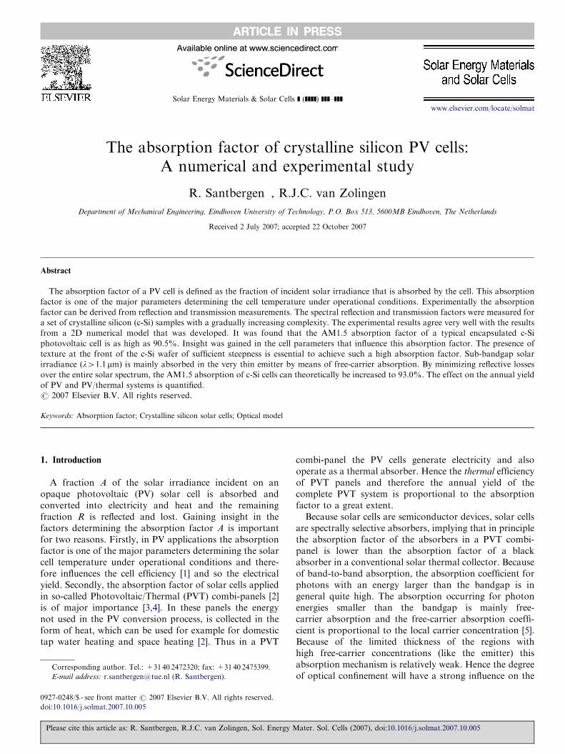
ARTICLE IN PRESS
0927-0248/$ - se
doi:10.1016/j.so
�CorrespondE-mail addr
Please cite thi
Solar Energy Materials & Solar Cells ] (]]]]) ]]]–]]]
www.elsevier.com/locate/solmat
The absorption factor of crystalline silicon PV cells:A numerical and experimental study
R. Santbergen�, R.J.C. van Zolingen
Department of Mechanical Engineering, Eindhoven University of Technology, P.O. Box 513, 5600MB Eindhoven, The Netherlands
Received 2 July 2007; accepted 22 October 2007
Abstract
The absorption factor of a PV cell is defined as the fraction of incident solar irradiance that is absorbed by the cell. This absorption
factor is one of the major parameters determining the cell temperature under operational conditions. Experimentally the absorption
factor can be derived from reflection and transmission measurements. The spectral reflection and transmission factors were measured for
a set of crystalline silicon (c-Si) samples with a gradually increasing complexity. The experimental results agree very well with the results
from a 2D numerical model that was developed. It was found that the AM1.5 absorption factor of a typical encapsulated c-Si
photovoltaic cell is as high as 90.5%. Insight was gained in the cell parameters that influence this absorption factor. The presence of
texture at the front of the c-Si wafer of sufficient steepness is essential to achieve such a high absorption factor. Sub-bandgap solar
irradiance ðl41:1mmÞ is mainly absorbed in the very thin emitter by means of free-carrier absorption. By minimizing reflective losses
over the entire solar spectrum, the AM1.5 absorption of c-Si cells can theoretically be increased to 93.0%. The effect on the annual yield
of PV and PV/thermal systems is quantified.
r 2007 Elsevier B.V. All rights reserved.
Keywords: Absorption factor; Crystalline silicon solar cells; Optical model
1. Introduction
A fraction A of the solar irradiance incident on anopaque photovoltaic (PV) solar cell is absorbed andconverted into electricity and heat and the remainingfraction R is reflected and lost. Gaining insight in thefactors determining the absorption factor A is importantfor two reasons. Firstly, in PV applications the absorptionfactor is one of the major parameters determining the solarcell temperature under operational conditions and there-fore influences the cell efficiency [1] and so the electricalyield. Secondly, the absorption factor of solar cells appliedin so-called Photovoltaic/Thermal (PVT) combi-panels [2]is of major importance [3,4]. In these panels the energynot used in the PV conversion process, is collected in theform of heat, which can be used for example for domestictap water heating and space heating [2]. Thus in a PVT
e front matter r 2007 Elsevier B.V. All rights reserved.
lmat.2007.10.005
ing author. Tel.: +3140 2472320; fax: +31 40 2475399.
ess: [email protected] (R. Santbergen).
s article as: R. Santbergen, R.J.C. van Zolingen, Sol. Energy M
combi-panel the PV cells generate electricity and alsooperate as a thermal absorber. Hence the thermal efficiencyof PVT panels and therefore the annual yield of thecomplete PVT system is proportional to the absorptionfactor to a great extent.Because solar cells are semiconductor devices, solar cells
are spectrally selective absorbers, implying that in principlethe absorption factor of the absorbers in a PVT combi-panel is lower than the absorption factor of a blackabsorber in a conventional solar thermal collector. Becauseof band-to-band absorption, the absorption coefficient forphotons with an energy larger than the bandgap is ingeneral quite high. The absorption occurring for photonenergies smaller than the bandgap is mainly free-carrier absorption and the free-carrier absorption coeffi-cient is proportional to the local carrier concentration [5].Because of the limited thickness of the regions withhigh free-carrier concentrations (like the emitter) thisabsorption mechanism is relatively weak. Hence the degreeof optical confinement will have a strong influence on the
ater. Sol. Cells (2007), doi:10.1016/j.solmat.2007.10.005
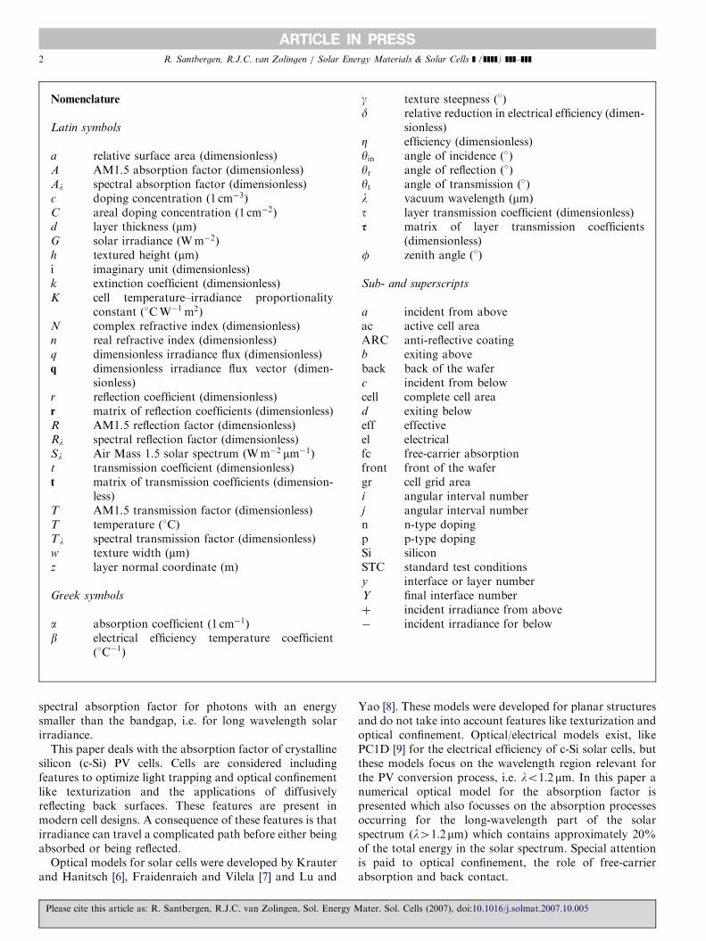
ARTICLE IN PRESS
Nomenclature
Latin symbols
a relative surface area (dimensionless)A AM1.5 absorption factor (dimensionless)Al spectral absorption factor (dimensionless)c doping concentration ð1 cm�3ÞC areal doping concentration ð1 cm�2Þd layer thickness ðmmÞG solar irradiance ðWm�2Þh textured height ðmmÞi imaginary unit (dimensionless)k extinction coefficient (dimensionless)K cell temperature–irradiance proportionality
constant ð�CW�1 m2Þ
N complex refractive index (dimensionless)n real refractive index (dimensionless)q dimensionless irradiance flux (dimensionless)q dimensionless irradiance flux vector (dimen-
sionless)r reflection coefficient (dimensionless)r matrix of reflection coefficients (dimensionless)R AM1.5 reflection factor (dimensionless)Rl spectral reflection factor (dimensionless)Sl Air Mass 1.5 solar spectrum ðWm�2 mm�1Þt transmission coefficient (dimensionless)t matrix of transmission coefficients (dimension-
less)T AM1.5 transmission factor (dimensionless)T temperature ð�CÞTl spectral transmission factor (dimensionless)w texture width ðmmÞz layer normal coordinate (m)
Greek symbols
a absorption coefficient ð1 cm�1Þb electrical efficiency temperature coefficient
ð�C�1Þ
g texture steepness ð�Þd relative reduction in electrical efficiency (dimen-
sionless)Z efficiency (dimensionless)yin angle of incidence ð�Þyr angle of reflection ð�Þyt angle of transmission ð�Þl vacuum wavelength ðmmÞt layer transmission coefficient (dimensionless)s matrix of layer transmission coefficients
(dimensionless)f zenith angle ð�Þ
Sub- and superscripts
a incident from aboveac active cell areaARC anti-reflective coatingb exiting aboveback back of the waferc incident from belowcell complete cell aread exiting beloweff effectiveel electricalfc free-carrier absorptionfront front of the wafergr cell grid areai angular interval numberj angular interval numbern n-type dopingp p-type dopingSi siliconSTC standard test conditionsy interface or layer numberY final interface numberþ incident irradiance from above� incident irradiance for below
R. Santbergen, R.J.C. van Zolingen / Solar Energy Materials & Solar Cells ] (]]]]) ]]]–]]]2
spectral absorption factor for photons with an energysmaller than the bandgap, i.e. for long wavelength solarirradiance.
This paper deals with the absorption factor of crystallinesilicon (c-Si) PV cells. Cells are considered includingfeatures to optimize light trapping and optical confinementlike texturization and the applications of diffusivelyreflecting back surfaces. These features are present inmodern cell designs. A consequence of these features is thatirradiance can travel a complicated path before either beingabsorbed or being reflected.
Optical models for solar cells were developed by Krauterand Hanitsch [6], Fraidenraich and Vilela [7] and Lu and
Please cite this article as: R. Santbergen, R.J.C. van Zolingen, Sol. Energy M
Yao [8]. These models were developed for planar structuresand do not take into account features like texturization andoptical confinement. Optical/electrical models exist, likePC1D [9] for the electrical efficiency of c-Si solar cells, butthese models focus on the wavelength region relevant forthe PV conversion process, i.e. lo1:2mm. In this paper anumerical optical model for the absorption factor ispresented which also focusses on the absorption processesoccurring for the long-wavelength part of the solarspectrum ðl41:2mmÞ which contains approximately 20%of the total energy in the solar spectrum. Special attentionis paid to optical confinement, the role of free-carrierabsorption and back contact.
ater. Sol. Cells (2007), doi:10.1016/j.solmat.2007.10.005
ARTICLE IN PRESSR. Santbergen, R.J.C. van Zolingen / Solar Energy Materials & Solar Cells ] (]]]]) ]]]–]]] 3
First the optical model obtained is validated bycomparing the numerical results to results of opticalmeasurements carried out on various c-Si PV cellstructures. The model is then used to acquire quantitativeinsight in the contributions of the various absorptionmechanisms to the total absorption factor. c-Si solar cellsposses various design features affecting the absorptionfactor such as the type of front texture or the metal gridcoverage. The optical model is also used to investigate theabsorption factor of various solar cell designs. It will turnout that the pursuit of high electrical efficiencies in mostcases will result in an increase of their absorption factorand thus in an increase of the operational cell temperature.Annual yield models exist for PV [10] and PVT systems[11–13]. Both a PV and a PVT model will be used to studyeffects of the increased temperature on the annual yield.
102
104
106
α c−S
i (cm
−1)
2. Model description
In the numerical model a PV cell is represented by a two-dimensional (2D) multi-layer structure as shown in Fig. 1.The laws of optics are used to determine how incidentirradiance propagates through this structure. The absorbedfraction at wavelength l, i.e. the spectral absorption factorAl, is determined taking into account the effects of an anti-reflective (AR) coating, scattering by rough interfaces andmultiple reflections of trapped irradiance. This is done for arange of wavelengths, i.e. l ¼ 0:323:0mm. By averagingthe spectral absorption factor Al over the AM1.5 spectrumSl [14], the (AM1.5) absorption factor A is found,
A ¼
RAlSl dlR
Sl dl. (1)
First in Section 2.1 the optical constants that play a role areintroduced. In Section 2.2 it is explained how the spectralabsorption factor Al can be determined for a multi-layerconfiguration with flat and smooth interfaces. This is only asimple representation of a PV cell in which the importantoptical effects of rough and textured interfaces are not yettaken into account. Next in Section 2.3 it is indicated howthese effects can be characterized using a matrix description.Finally in Section 2.4 it will be explained how these matricesare used in the extended model, to determine Al for morerealistic representations of a PV cell.
glass
EVA
p-layer
n-layer
metal
encapsulation AR coating
silicon wafer
back contact
Fig. 1. A schematic cross-section of an encapsulated c-Si PV cell.
Please cite this article as: R. Santbergen, R.J.C. van Zolingen, Sol. Energy M
2.1. The optical constants
In the model a PV cell is represented by a multi-layerstructure, each layer being characterized by a complexrefractive index,
N ¼ n� ik, (2)
where both the real refractive index n and the extinctioncoefficient k are functions of l. For most materials nðlÞ andkðlÞ can be found in literature [15,16]. Note that theabsorption coefficient a and the extinction coefficient k arerelated by,
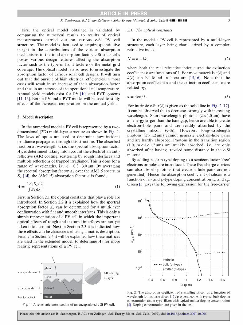
a ¼ 4pk=l. (3)
For intrinsic c-Si aðlÞ is given as the solid line in Fig. 2 [17].It can be observed that a decreases strongly with increasingwavelength. Short-wavelength photons ðlo1:0 mmÞ havean energy larger than the bandgap, hence are able to createelectron–hole pairs and are readily absorbed by thecrystalline silicon (c-Si). However, long-wavelengthphotons ðl41:2 mmÞ cannot generate electron-hole pairsand are hardly absorbed. Photons in the transition regionð1:0 mmolo1:2mmÞ are weakly absorbed, i.e. are onlyabsorbed after having traveled some distance in the c-Simaterial.By adding n- or p-type doping to a semiconductor ‘free’
electrons or holes are introduced. These free charge carrierscan also absorb photons (but electron–hole pairs are notgenerated). Hence the absorption coefficient of silicon is afunction of n- and p-type doping concentration cn and cp.Green [5] gives the following expression for the free-carrier
0.4 0.6 0.8 1 1.2 1.4 1.6
10−2
100
λ (μ m)
intrinsic
bulk (p−type)
emitter (n−type)
Fig. 2. The absorption coefficient of crystalline silicon as a function of
wavelength for intrinsic silicon [17], p-type silicon with typical bulk doping
concentration and n-type silicon with typical emitter doping concentration
[5]. Doping concentration are given in the text.
ater. Sol. Cells (2007), doi:10.1016/j.solmat.2007.10.005

ARTICLE IN PRESSR. Santbergen, R.J.C. van Zolingen / Solar Energy Materials & Solar Cells ] (]]]]) ]]]–]]]4
absorption coefficient,
afc ¼ 2:6� 10�18cnl3þ 2:7� 10�18cpl
2, (4)
where afc is given in cm�1, l in mm and cn and cp in cm�3.The p-type doping concentration in the bulk of the wafer
typically is 1:0� 1016 cm�3 and the maximum n-typedoping concentration in the emitter typically is 3:3�1020 cm�3 [18]. For these typical doping concentrations theabsorption coefficient ac�Si is illustrated in Fig. 2. Byevaluation of the product of these absorption coefficientsand the corresponding layer thickness, it is found that forl41:2mm free-carrier absorption is dominant and hencethis effect is taken into account.
2.2. The net-radiation method
A multi-layer configuration is a simple representation ofa PV cell. For now the interfaces are assumed to be flat andsmooth, so reflections are specular and the (unidirectional)net-radiation method [19] can be used to find Al. In thismethod at each interface y, four fluxes qy;x are definedwhere x ¼ a; b; c; d (see left panel of Fig. 3). Each fluxcontains the net-radiation, i.e. the contributions of multiplereflections between the interfaces. For each interface y, thefollowing relationships exist between the net-radiationfluxes,
qy;a ¼ ty�1 � qy�1;d ;
qy;b ¼ ry � qy;a þ ty � qy;c;
qy;c ¼ ty � qyþ1;b;
qy;d ¼ ry � qy;c þ ty � qy;a;
8>>>><>>>>:
(5)
where ry is the intensity coefficient of reflection andty ¼ 1� ry. These coefficients are determined using Fres-nell’s laws [20] in which the different polarization states are
inter-face
layer
1
1
Y
y-1
y-1
y
y
qy,a qy,bq1
y,bq2
y,b
q3y,b
qy,c qy,d
qy-1,d
qY,c
q1,a
qy+1,b
y+1
Y-1
Fig. 3. A schematic overview of the fluxes defined at each interface in the
net-radiation method. Left: the unidirectional model, as described in
Section 2.2. Right: the multi-directional model, as described in Section 2.4.
Please cite this article as: R. Santbergen, R.J.C. van Zolingen, Sol. Energy M
treated separately. Further
ty ¼ e�aydy= cosfy , (6)
is the transmission coefficient of layer y and ay and dy arethe layer’s absorption coefficient and thickness, respec-tively. The distance irradiance travels in a single passthrough layer y is given by dy= cosfy, where fy is thepropagation direction of irradiance in the layer, measuredfrom the interface normal direction. No irradiance isincident from below so qY ;c ¼ 0, where Y indicates the finalinterface. Because all fluxes are proportional to q1;a, it willbe convenient to non-dimensionalize the fluxes, so thatq1;a ¼ 1.The unknown fluxes can be found by solving the set of
linear equations (5) and the spectral absorption factor oflayer y is given by,
Al;y ¼ qy;d � qyþ1;a þ qyþ1;b � qy;c. (7)
By summing the spectral absorption factor of theindividual layers, the spectral absorption factor of theentire multi-layer configuration is found,
Al ¼XY�1y¼1
Al;y. (8)
The spectral reflection and transmission factors aregiven by,
Rl ¼ q1;b, (9)
Tl ¼ qY ;d , (10)
and it can be checked that in this method energy isautomatically conserved,
Rl þ Al þ Tl � 1. (11)
Net-radiation flux q contains contributions originatingfrom multiple reflections and its intensity is assumed to bethe sum of all contributions. This is only correct if nointerference effects occur, i.e. if the optical thickness ofeach layer exceeds the coherence length of the irradiancebeing approximately 1mm for solar irradiance [20]. In thec-Si PV cells considered here, this is true for all layersexcept for the AR coating, whose working principle isjust based on the interference effect. Hence the effectivereflection coefficient rARC of the AR coating is firstcalculated separately, taking into account the interferenceeffect [21]. In the multi-layer system the coating is thenrepresented as a single interface, characterized by rARC.
2.3. Light scattering at interfaces
The spectral absorption factor Al of weakly absorbedirradiance depends very much on the degree of opticalconfinement. If confinement is poor, a large part of theirradiance that has entered the cell will escape after a fewpasses, resulting in a low Al. However, irradiance scatteredinto oblique directions can be trapped inside the cellfor many passes, increasing the pathlength and hence Al.
ater. Sol. Cells (2007), doi:10.1016/j.solmat.2007.10.005
ARTICLE IN PRESSR. Santbergen, R.J.C. van Zolingen / Solar Energy Materials & Solar Cells ] (]]]]) ]]]–]]] 5
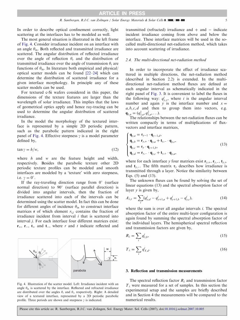
In order to describe optical confinement correctly, lightscattering at the interfaces has to be modeled as well.
The most general situation is illustrated in the left frameof Fig. 4. Consider irradiance incident on an interface withan angle yin. Both reflected and transmitted irradiance arescattered. The angular distribution of reflected irradianceover the angle of reflection yr and the distribution oftransmitted irradiance over the angle of transmission yt arefunctions of yin. In literature both empirical and physical/optical scatter models can be found [22–24] which candetermine the distribution of scattered irradiance for agiven interface morphology. In principle any of thesescatter models can be used.
For textured c-Si wafers considered in this paper, thedimensions of the texture features are larger than thewavelength of solar irradiance. This implies that the lawsof geometrical optics apply and hence ray-tracing can beused to determine the angular distribution of scatteredirradiance.
In the model the morphology of the textured inter-face is represented by a simple 2D periodic pattern,such as the parabolic pattern indicated in the rightpanel of Fig. 4. Effective steepness g is a model parameterdefined by,
tan g ¼ h=w, (12)
where h and w are the feature height and width,respectively. Besides the parabolic texture other 2Dperiodic texture profiles can be modeled and smoothinterfaces are modeled by a ‘texture’ with zero steepness,i.e. g ¼ 0�.
If the ray-traveling direction range from 0� (surfacenormal direction) to 90� (surface parallel direction) isdivided into angular intervals, then the fraction ofirradiance scattered into each of the intervals can bedetermined using the scatter model. In fact this can be donefor different angles of incidence yin to construct interfacematrices r of which element ri;j contains the fraction ofirradiance incident from interval i that is scattered intointerval j. For each interface four different matrices exist:rþ, r�, tþ and t�, where r and t indicate reflected and
γ
w
h
θin θr
θt
parabola
Fig. 4. Illustration of the scatter model. Left: Irradiance incident with an
angle yin is scattered by the interface. Reflected and refracted irradiance
are distributed over the angles yr and yt, respectively. Right: A detailed
view of a textured interface, represented by a 2D periodic parabolic
profile. Three periods are shown and steepness g is indicated.
Please cite this article as: R. Santbergen, R.J.C. van Zolingen, Sol. Energy M
transmitted (refracted) irradiance and þ and � indicateincident irradiance coming from above and below theinterface. These interface matrices will be used in the so-called multi-directional net-radiation method, which takesinto account scattering of irradiance.
2.4. The multi-directional net-radiation method
In order to incorporate the effect of irradiance sca-ttered in multiple directions, the net-radiation method(described in Section 2.2) is extended. In the multi-directional net-radiation method fluxes are defined ateach angular interval as schematically indicated in theright panel of Fig. 3. It is convenient to label the fluxes inthe following way: qi
y;x, where i is the angular intervalnumber and again y is the interface number and x ¼
a; b; c; d and then to group them into vectors, e.g.q1;a ¼ ðq
11;a; q
21;a; . . .Þ.
The relationships between the net-radiation fluxes can bewritten compactly in terms of multiplications of flux-vectors and interface matrices,
qy;a ¼ sy�1 � qy�1;d ;
qy;b ¼ ry;þ � qy;a þ ty;� � qy;c;
qy;c ¼ sy � qyþ1;b;
qy;d ¼ ry;� � qy;c þ ty;þ � qy;a;
8>>>><>>>>:
(13)
where for each interface y four matrices exist ry;þ, ry;�, ty;þand ty;�. The fifth matrix sy describes how irradiance istransmitted through a layer. Notice the similarity betweenEqs. (5) and (13).The unknown fluxes can be found by solving the set of
linear equations (13) and the spectral absorption factor oflayer y is given by,
Al;y ¼X
i
ðqiy;d � qi
yþ1;a þ qiyþ1;b � qi
y;cÞ, (14)
where the sum is over all angular intervals i. The spectralabsorption factor of the entire multi-layer configuration isagain found by summing the spectral absorption factor ofthe individual layers. The hemispherical spectral reflectionand transmission factors are given by,
Rl ¼X
i
qi1;b, (15)
Tl ¼X
i
qiY ;d . (16)
3. Reflection and transmission measurements
The spectral reflection factor Rl and transmission factorTl were measured for a set of samples. In this section theexperimental setup and the samples are briefly describedand in Section 4 the measurements will be compared to thenumerical results.
ater. Sol. Cells (2007), doi:10.1016/j.solmat.2007.10.005

ARTICLE IN PRESS
0.4 0.6 0.8 1 1.2 1.4 1.60
0.1
0.2
0.3
0.4
0.5
0.6
0.7
0.8
0.9
1
λ (μm)1
−Rλ,
Tλ
(−)
meas. 1−Rλ
meas. Tλsim. 1−Rλ
sim. Tλ
Rλ
Aλ
Tλ
reflected
absorbed
transmitted
1
Fig. 5. Measured and simulated 1�Rl and Tl as a function of l for a
polished wafer (sample 1).
R. Santbergen, R.J.C. van Zolingen / Solar Energy Materials & Solar Cells ] (]]]]) ]]]–]]]6
3.1. Experimental set-up
To measure the hemispherical reflectance Rl of a sample,a Labsphere RTC 060 SF integrating sphere is used whichcollects the reflected irradiance scattered in all hemisphe-rical directions. The intensity inside the Spectraflects
coated sphere is proportional to Rl and is measured byan Instruments Systems spectroradiometer (Spectro 320R5). Using this setup, besides the hemispherical reflectanceR, the hemispherical transmittance T can be determinedwith a 1% inaccuracy for 0:33olo1:4mm.
3.2. Samples
A complete c-Si PV cell is a complex optical device inwhich several optical effects occur simultaneously. In orderto validate the model a set of samples was prepared with agradually increasing complexity. In this way one opticaleffect is introduced at the time and it can be checkedwhether this effect is captured by the model. Next a briefdescription of samples 1–5 is given and the details are givenin Table 1.
All samples are c-Si wafers and have a p-type boron bulkdoping concentration of 1:0� 1016 cm�3, resulting in aresistivity of 1:5O cm. Sample 1 is a reference sample ofCzochralski (cz) mono-crystalline silicon of 500 mm thick-ness. Both sides are polished to flat and smooth interfaces.Samples 2–5 are multi-crystalline (mc) silicon texturedwafers of approximately 300mm thickness. They aretextured by means of an acid texture etch, resulting in apitted surface [25] at the front and to a lesser extent also atthe back.
Samples 3–5 have a phosphorous emitter of 62O&.Details of the emitter will be given in Section 4.3. Samples 4and 5 have a standard plasma enhanced chemical vapordeposition (PECVD) silicon-nitride ðSi3N4Þ AR coatingwith a thickness of typically 80 nm. Sample 5 has astandard aluminium back contact, which was screen-printed on the backside of the wafer and then alloyed.
4. Results
In this section the numerical and experimental results arecompared. This is done for the samples given in Table 1.
Table 1
Crystalline silicon samples 1–5
Nr Material Thickness
ðmmÞInterface Emitter ARC Back
contact
1 cz Si 500 Polished – – –
2 mc Si 325 Textured – – –
3 mc Si 318 Textured 62O& – –
4 mc Si 309 Textured 62O& Yes –
5 mc Si 325 Textured 62O& Yes Al
alloyed
cz ¼ Czochralski mono-crystalline, mc ¼ multi-crystalline.
Please cite this article as: R. Santbergen, R.J.C. van Zolingen, Sol. Energy M
In the following figures 1� Rl and Tl are plotted so thearea in between corresponds to the spectral absorptionfactor Al ¼ 1� Rl � Tl. The numerical results are plottedin the same way. Measurement results are indicated bysymbols ð�; ,Þ and numerical results by lines.
4.1. Polished wafer
In Fig. 5 the results are shown for sample 1, the doublesided polished wafer. This measurement illustrates that forlo1:0mm the wafer is opaque ðTl ¼ 0Þ while for l41:2mmthe wafer is transparent ðAl � 0Þ. The increase in Rl forl41:2mm (indicated by arrow 1) is caused by thetransparency of the wafer, allowing irradiance to beinternally reflected by the back interface. Both front andback surface were modeled as smooth interfaces. As can beseen the numerical results agree very well with theexperiments.
4.2. Textured wafer
When the measurement results of the textured sample 2(Fig. 6) are compared to the previous sample, the twoadvantages of texture can be seen. Firstly, in the opaqueregime ðlo1:0 mmÞ Rl is reduced as a result of improvedincoupling (indicated by arrow 2). Secondly, in thetransparent regime ðl41:2mmÞ Al has increased (indicatedby arrow 3) as a result of the increased pathlength causedby the improved optical confinement.As described in Section 2.3, textured interfaces are
modeled as a parabolic profile and by numerically varyingthe profile steepness g, the amount of incoupling and hencethe ‘effective’ reflection coefficient of the textured interface
ater. Sol. Cells (2007), doi:10.1016/j.solmat.2007.10.005

ARTICLE IN PRESS
0.4 0.6 0.8 1 1.2 1.4 1.60
0.1
0.2
0.3
0.4
0.5
0.6
0.7
0.8
0.9
1
λ (μm)
1−R
λ, T
λ (−
)
meas. 1−Rλmeas. Tλsim. 1−Rλsim. Tλ
4
Fig. 7. Measured and simulated 1�Rl and Tl as a function of l for a
textured wafer with emitter (sample 3).
2
3
0.4 0.6 0.8 1 1.2 1.4 1.60
0.1
0.2
0.3
0.4
0.5
0.6
0.7
0.8
0.9
1
λ (μm)
1−R
λ, T
λ (−
)
meas. Tλmeas. 1−Rλsim. 1−Rλsim. Tλ
Fig. 6. Measured and simulated 1� Rl and Tl as a function of l for a
textured wafer (sample 2).
R. Santbergen, R.J.C. van Zolingen / Solar Energy Materials & Solar Cells ] (]]]]) ]]]–]]] 7
can be controlled. By comparing the measured values ofRl¼1:0 mm for both the front and the backside of the texturedwafer to the results of a ray-tracing analysis it was foundthat a texture steepness of 41� and 32� are required for thefront and the back, respectively. Hence gfront ¼ 41� andgback ¼ 32� will be used to model the front and backinterfaces of all textured wafers (samples 2–5). The smalldeviation for l41:0mm is discussed in the next section.
It can be seen that both the reduction of Rlo1:0 mm andthe increase of Al41:2 mm are also found numerically. Thismeans that the parabolic profile, besides the incouplingeffect, also captures the scattering and trapping effect quitewell. Note that the parabolic profile was used because itbest resembles the pitted profile of an acid etch texturedwafer surface. If texture is represented by a differentprofile, such as a zigzag profile, then there is less agreementbetween model and measurement. This indicates thatbesides the steepness, the shape of the texture profile isimportant as well.
4.3. Emitter
Sample 3 is identical to the previous one with aphosphorous emitter with a sheet resistance of 62O&
added. The Hall-effect is commonly exploited to determinethe electrically active doping concentration. Bisschop [18]has determined the doping profile cðzÞ of similar emittersusing stripping Hall measurements, where z is the distanceto the wafer front. The emitter profiles have a maximumdoping concentration cð0Þ ¼ 3:3� 1020 cm�3 at the surfaceand their areal doping concentration C ¼
RcðzÞdz ¼
1:8� 1015 cm�2.
Please cite this article as: R. Santbergen, R.J.C. van Zolingen, Sol. Energy M
From the optical measurement results (Fig. 7) it can beseen that for lo1:0mm there is no difference with theprevious sample. However, for l41:2mm, Al has increasedtremendously because of free-carrier absorption in theemitter (indicated by arrow 4). Note that though thisabsorption mechanism increases the AM1.5 absorptionfactor significantly, the electrical efficiency is hardlyaffected, since no additional electron–hole pairs aregenerated.Since the free-carrier absorption coefficient is linear in
doping concentrations cn ðcpÞ, the amount of free-carrier absorption only depends on the areal dopingconcentration C. Hence the emitter was modeled as asingle layer with a constant doping concentration equal topeak concentration cnð0Þ and an effective thicknessd ¼ C=cnð0Þ ¼ 55 nm.Similar to the experiments, the model results show that
the addition of an emitter results in a large increase inAl41:2 mm (Fig. 7).
4.4. AR coating
Sample 4 is identical to the previous one, only an ARcoating was added to the front. From the experimentalresults (Fig. 8) it can be seen that for l � 0:7mm thecoating reduces Rl to very low values (indicated by arrow5). This is a well known interference effect exploited by ARcoatings. This effect is modeled with a coating thickness of84 nm and good agreement is found. There is a smalldeviation for l ¼ 0:4 mm (indicated by arrow 6) whichwould disappear if a slightly higher optical absorption
ater. Sol. Cells (2007), doi:10.1016/j.solmat.2007.10.005
ARTICLE IN PRESS
0
0.1
0.2
0.3
0.4
0.5
0.6
0.7
0.8
0.9
1
1−R
λ, T
λ (−
)
meas.
sim., esc. fact. = 1
sim., esc. fact. = 0.4
0.4 0.6 0.8 1 1.2 1.4 1.6
λ (μm)
Fig. 9. Measured and simulated 1� Rl as a function of l for a textured
wafer with emitter, AR coating and back contact (sample 5). The solid line
represents a simulation without correction (i.e. with an escape factor of 1)
and the dashed line represents a corrected simulation with an escape factor
of 0.4.
0.4 0.6 0.8 1 1.2 1.4 1.60
0.1
0.2
0.3
0.4
0.5
0.6
0.7
0.8
0.9
λ (μm)
Aλ
(−)
reflected
9.5%
glass 3.2%
aluminium
3.5%
fca bulk
silicon 0.9%
free carrier abs.
emitter 10.6%
band−to−band
abs. silicon 70.4%
ARC2.1%
Fig. 10. Area plot of the spectral absorption factor Al for each layer of
configuration 6. The AM1.5 absorption factors are also given for each
layer separately. The total absorption factor is 90.5%.
0.4 0.6 0.8 1 1.2 1.4 1.60
0.1
0.2
0.3
0.4
0.5
0.6
0.7
0.8
0.9
1
λ (μm)
1−R
λ, T
λ (−
)
sim. 1−Rλ
sim. Tλ
meas. 1−Rλ
meas. Tλ
5
6
Fig. 8. Measured and simulated 1� Rl and Tl as a function of l for a
textured wafer with emitter and AR coating (sample 4).
R. Santbergen, R.J.C. van Zolingen / Solar Energy Materials & Solar Cells ] (]]]]) ]]]–]]]8
in the Si3N4 coating is assumed. It is known thatfor lo0:4mm there can be some absorption in the coa-ting and the exact amount depends on the depositionconditions [26].
Please cite this article as: R. Santbergen, R.J.C. van Zolingen, Sol. Energy M
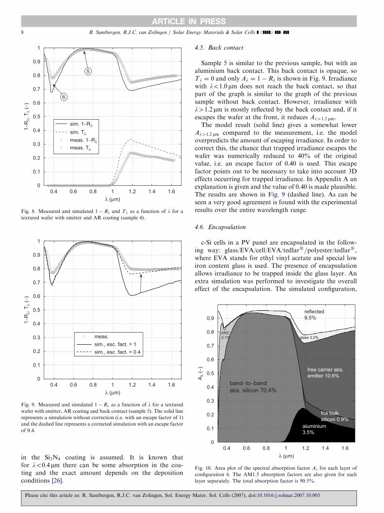
4.5. Back contact
Sample 5 is similar to the previous sample, but with analuminium back contact. This back contact is opaque, soTl ¼ 0 and only Al ¼ 1� Rl is shown in Fig. 9. Irradiancewith lo1:0 mm does not reach the back contact, so thatpart of the graph is similar to the graph of the previoussample without back contact. However, irradiance withl41:2mm is mostly reflected by the back contact and, if itescapes the wafer at the front, it reduces Al41:2 mm.The model result (solid line) gives a somewhat lower
Al41:2 mm compared to the measurement, i.e. the modeloverpredicts the amount of escaping irradiance. In order tocorrect this, the chance that trapped irradiance escapes thewafer was numerically reduced to 40% of the originalvalue, i.e. an escape factor of 0.40 is used. This escapefactor points out to be necessary to take into account 3Deffects occurring for trapped irradiance. In Appendix A anexplanation is given and the value of 0.40 is made plausible.The results are shown in Fig. 9 (dashed line). As can beseen a very good agreement is found with the experimentalresults over the entire wavelength range.
4.6. Encapsulation
c-Si cells in a PV panel are encapsulated in the follow-ing way: glass/EVA/cell/EVA/tedlars=polyester/tedlars,where EVA stands for ethyl vinyl acetate and special lowiron content glass is used. The presence of encapsulationallows irradiance to be trapped inside the glass layer. Anextra simulation was performed to investigate the overalleffect of the encapsulation. The simulated configuration,
ater. Sol. Cells (2007), doi:10.1016/j.solmat.2007.10.005
ARTICLE IN PRESS
0.87
0.88
0.89
0.9
0.91
0.92
(−)
R. Santbergen, R.J.C. van Zolingen / Solar Energy Materials & Solar Cells ] (]]]]) ]]]–]]] 9
denoted as configuration 6, has a 3mm thick low ironcontent glass cover added. It is assumed that the opticalproperties of EVA are similar to those of glass and hencethe EVA layer was not modeled separately.
The results are shown in Fig. 10. The spectral absorptionfactor is indicated for each layer separately. The remainingwhite area represents Rl. It can be seen that for short-wavelength solar irradiance ðlo1:1mmÞ the band-to-bandabsorption is dominant, while for long-wavelength solarirradiance free-carrier absorption in the emitter is domi-nant. Smaller fractions of the AM1.5 spectrum areabsorbed in the glass cover, in the AR coating and in theback contact.
4.7. Comparison of experimental and numerical results
In Table 2 an overview is given of the performedsimulations. The simulated absorption factors are com-pared to the ones derived from the experiments on samples1–5. It can be seen that the absorption factor of a barepolished wafer (sample 1) is only 49.5%. Because ofreduction of reflective losses by texture and AR coatingand by absorption in emitter and back contact thisincreases to as much as 90.2% for an almost complete cell(sample 5).
The numerical model is completely based on the laws of(geometrical) optics. Only the texture steepness g is used asparameter to fit the amount of incoupling of irradiance forl41:0mm to the measured values. For l41:0mm trappingof irradiance inside the wafer is an important effect, whichhas essentially a three-dimensional (3D) nature while themodel is 2D. But even without correcting for 3D effects inlight trapping, the deviations in AM1.5 absorption factor A
from the experimental values are at most 3.6%. Aftercompensating for the 3D effects by means of an escapefactor, the deviation is even reduced to only 1.2%. Theremaining deviation originates mainly from the blue part ofthe solar spectrum ðl � 0:4 mmÞ and is caused by someextra absorption in the AR coating, not taken into accountby the model.
The effect of encapsulation was only investigatednumerically (configuration 6). By comparing the absorp-tion factors for configurations 5 and 6 it can be seen that
Table 2
The numerical and the corresponding measured AM1.5 absorption
factor A
Nr Description Anum (%) Aexp (%)
1 Bare polished c-Si wafer 49.9 49.5
2 þ Texture (acid etch) 63.4 64.1
3 þ Emitter ð62O&Þ 69.7 71.4
4 þ AR coating ðSi3N4Þ 82.3 85.8
5 þ Back contact (Al) 86.6 90.2
89:0�
6 þ Encapsulation 90:5� –
For numerical results marked with *, an escape factor of 0.4 was used.
Please cite this article as: R. Santbergen, R.J.C. van Zolingen, Sol. Energy M
encapsulation increases the absorption factor from 89.0%to 90.5%. This encapsulated configuration will be used asreference configuration in Section 5.
5. Influence of the cell design
The influence of the cell design on the absorptionfactor will be investigated using the numerical model inSections 5.1–5.4, e.g. by varying the steepness of thetexture, the strength of the emitter and the reflectioncoefficient of the back contact. Each time configuration 6,which has encapsulation and an escape factor of 0.4, will beused as a starting point. This information will be used inSections 5.5 and 5.6, where the effect of the absorptionfactor on the annual electrical yield of PV systems and boththe annual electrical and thermal yield of PVT systems isdiscussed.
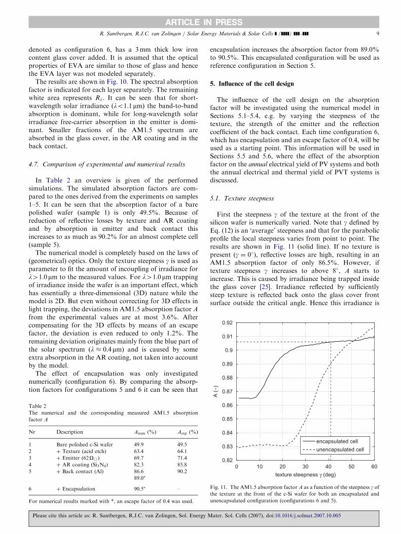
5.1. Texture steepness
First the steepness g of the texture at the front of thesilicon wafer is numerically varied. Note that g defined byEq. (12) is an ‘average’ steepness and that for the parabolicprofile the local steepness varies from point to point. Theresults are shown in Fig. 11 (solid line). If no texture ispresent ðg ¼ 0�Þ, reflective losses are high, resulting in anAM1.5 absorption factor of only 86.5%. However, iftexture steepness g increases to above 8�, A starts toincrease. This is caused by irradiance being trapped insidethe glass cover [25]. Irradiance reflected by sufficientlysteep texture is reflected back onto the glass cover frontsurface outside the critical angle. Hence this irradiance is
0 10 20 30 40 50 600.82
0.83
0.84
0.85
0.86
texture steepness γ (deg)
A
encapsulated cell
unencapsulated cell
Fig. 11. The AM1.5 absorption factor A as a function of the steepness g ofthe texture at the front of the c-Si wafer for both an encapsulated and
unencapsulated configuration (configurations 6 and 5).
ater. Sol. Cells (2007), doi:10.1016/j.solmat.2007.10.005

ARTICLE IN PRESS
0 0.2 0.4 0.6 0.8 10.89
0.895
0.9
0.905
0.91
0.915
0.92
0.925
0.93
0.935
0.94
rback (−)
A (
−)
AlCr Ni
Fig. 13. The AM1.5 absorption factor A as a function of back contact
reflectance rback for an encapsulated configuration (configuration 6).
R. Santbergen, R.J.C. van Zolingen / Solar Energy Materials & Solar Cells ] (]]]]) ]]]–]]]10
totally internally reflected back into the forward direction.This guarantees incident irradiance at least two chances ofentering the wafer before any chance of escaping the glassarises. Hence for a texture steepness of 8225� there is astrong increase in A to above 90%. Further increasing thesteepness to more than 25� only results in a small increasein A. This is in contrast with an unencapsulated cell, whichhas no glass cover to trap reflected irradiance. As a resultthe absorption factor remains low up to g ¼ 25� and thenincreases sharply, shown as the dashed line in Fig. 11.
5.2. Emitter strength
Since a significant part of long-wavelength irradiance isabsorbed by free-carrier absorption in the emitter, theeffect of emitter strength on the AM1.5 absorption factor A
is investigated. By varying the emitter thickness, the areal(integral) doping concentration and hence the correspond-ing sheet resistance can be varied. In Fig. 12 the absorptionfactor A is shown as a function of sheet resistance. In casethe emitter is omitted, the AM1.5 absorption factor is86.1%. A typical emitter increases this to between 90.2%(at 80O&) and to 91.2% (at 40O&).
5.3. Back contact reflectivity
Also the effect of back contact reflectivity on absorptionfactor A is investigated. Note that only long-wavelengthsolar irradiance ðl41:0mmÞ reaches the back contact andcan be affected by it. The value of rback is numericallyvaried between 0 and 1, i.e. between a perfectly absorbingand a perfectly reflecting back contact. The results areshown in Fig. 13. It can be seen that A varies between
20 40 60 80 1000.895
0.9
0.905
0.91
0.915
0.92
0.925
emitter sheet resistance (Ωsquare)
A (
−)
Fig. 12. The AM1.5 absorption factor A as a function of emitter sheet
resistance for an encapsulated configuration (configuration 6).
Please cite this article as: R. Santbergen, R.J.C. van Zolingen, Sol. Energy M
89.9% and 93.0%. The higher value corresponds to aperfectly absorbing back contact.The aluminium back contact used in the reference
configuration is very reflective, i.e. rback � 0:90. One couldconsider to use nickel (Ni) or chromium (Cr) instead ofaluminium (Al) as a back contact. Both from reflectionmeasurements carried out on a number of additionalsamples and from the Fresnel relations it follows that witha Ni back contact rback � 0:50 and with a Cr back contactrback � 0:30. From the results it can be derived that anencapsulated PV cell with a nickel or chromium backcontact would have an absorption factor as high as 92.3%or 92.7%, respectively. A consequence of the use of lessreflecting back contact materials is that the PV efficiencywill drop by approximately 0.3% absolute. This drop iscaused by the absorption of near bandgap solar irradiancewhich, if absorbed in the back contact, can no longergenerate photocurrent.
5.4. Metal coverage of front contact
Up till now only the active cell area was considered.However, a part of the PV cell can be covered by the frontcontact grid. So in order to determine the absorption factorof the entire PV cell ðAcellÞ a weighted average is taken ofthe active (ac) area absorption factor and the front contactgrid (gr) area absorption factors,
Acell ¼ aacAac þ agrAgr, (17)
where A is the absorption factor and a is the relativesurface area. Here the absorption factor of the standardconfiguration (configuration 6) is taken as active areaabsorption factor, i.e. Aac ¼ 90:5%. The spectral absorption
ater. Sol. Cells (2007), doi:10.1016/j.solmat.2007.10.005
ARTICLE IN PRESS
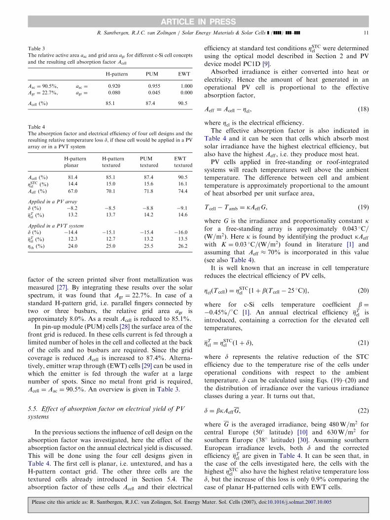
Table 3
The relative active area aac and grid area agr for different c-Si cell concepts
and the resulting cell absorption factor Acell
H-pattern PUM EWT
Aac ¼ 90:5%, aac ¼ 0.920 0.955 1.000
Agr ¼ 22:7%, agr ¼ 0.080 0.045 0.000
Acell (%) 85.1 87.4 90.5
Table 4
The absorption factor and electrical efficiency of four cell designs and the
resulting relative temperature loss d, if these cell would be applied in a PV
array or in a PVT system
H-pattern
planar
H-pattern
textured
PUM
textured
EWT
textured
Acell (%) 81.4 85.1 87.4 90.5
ZSTCel (%) 14.4 15.0 15.6 16.1
Aeff (%) 67.0 70.1 71.8 74.4
Applied in a PV array
d (%) �8.2 �8.5 �8.8 �9.1
ZTel (%) 13.2 13.7 14.2 14.6
Applied in a PVT system
d (%) �14.4 �15.1 �15.4 �16.0
ZTel (%) 12.3 12.7 13.2 13.5
Zth (%) 24.0 25.0 25.5 26.2
R. Santbergen, R.J.C. van Zolingen / Solar Energy Materials & Solar Cells ] (]]]]) ]]]–]]] 11
factor of the screen printed silver front metallization wasmeasured [27]. By integrating these results over the solarspectrum, it was found that Agr ¼ 22:7%. In case of astandard H-pattern grid, i.e. parallel fingers connected bytwo or three busbars, the relative grid area agr isapproximately 8.0%. As a result Acell is reduced to 85.1%.
In pin-up module (PUM) cells [28] the surface area of thefront grid is reduced. In these cells current is fed through alimited number of holes in the cell and collected at the backof the cells and no busbars are required. Since the gridcoverage is reduced Acell is increased to 87.4%. Alterna-tively, emitter wrap through (EWT) cells [29] can be used inwhich the emitter is fed through the wafer at a largenumber of spots. Since no metal front grid is required,Acell ¼ Aac ¼ 90:5%. An overview is given in Table 3.
5.5. Effect of absorption factor on electrical yield of PV
systems
In the previous sections the influence of cell design on theabsorption factor was investigated, here the effect of theabsorption factor on the annual electrical yield is discussed.This will be done using the four cell designs given inTable 4. The first cell is planar, i.e. untextured, and has aH-pattern contact grid. The other three cells are thetextured cells already introduced in Section 5.4. Theabsorption factor of these cells Acell and their electrical
Please cite this article as: R. Santbergen, R.J.C. van Zolingen, Sol. Energy M
efficiency at standard test conditions ZSTCel were determinedusing the optical model described in Section 2 and PVdevice model PC1D [9].Absorbed irradiance is either converted into heat or
electricity. Hence the amount of heat generated in anoperational PV cell is proportional to the effectiveabsorption factor,
Aeff ¼ Acell � Zel, (18)
where Zel is the electrical efficiency.The effective absorption factor is also indicated in
Table 4 and it can be seen that cells which absorb mostsolar irradiance have the highest electrical efficiency, butalso have the highest Aeff , i.e. they produce most heat.PV cells applied in free-standing or roof-integrated
systems will reach temperatures well above the ambienttemperature. The difference between cell and ambienttemperature is approximately proportional to the amountof heat absorbed per unit surface area,
Tcell � Tamb ¼ kAeffG, (19)
where G is the irradiance and proportionality constant kfor a free-standing array is approximately 0:043 �C=ðW=m2Þ. Here k is found by identifying the product kAeff
with K ¼ 0:03 �C=ðW=m2Þ found in literature [1] andassuming that Aeff � 70% is incorporated in this value(see also Table 4).It is well known that an increase in cell temperature
reduces the electrical efficiency of PV cells,
ZelðTcellÞ ¼ ZSTCel f1þ bðTcell � 25 �CÞg, (20)
where for c-Si cells temperature coefficient b ¼�0:45%=�C [1]. An annual electrical efficiency ZT
el isintroduced, containing a correction for the elevated celltemperatures,
ZTel ¼ ZSTCel ð1þ dÞ, (21)
where d represents the relative reduction of the STCefficiency due to the temperature rise of the cells underoperational conditions with respect to the ambienttemperature. d can be calculated using Eqs. (19)–(20) andthe distribution of irradiance over the various irradianceclasses during a year. It turns out that,
d ¼ bkAeffG, (22)
where G is the averaged irradiance, being 480W=m2 forcentral Europe (50� latitude) [10] and 630W=m2 forsouthern Europe (38� latitude) [30]. Assuming southernEuropean irradiance levels, both d and the correctedefficiency ZT
el are given in Table 4. It can be seen that, inthe case of the cells investigated here, the cells with thehighest ZSTCel also have the highest relative temperature lossd, but the increase of this loss is only 0.9% comparing thecase of planar H-patterned cells with EWT cells.
ater. Sol. Cells (2007), doi:10.1016/j.solmat.2007.10.005

ARTICLE IN PRESS
air (or glass)
silicon
γ
φ≈γ
Fig. A.1. Three rays reflected by the back contact under different zenith
angles f, reaching the textured front of the wafer. Only the ray having a
zenith angle close to the texture steepness, i.e. deviating less than the
critical angle, has a chance of escaping.
R. Santbergen, R.J.C. van Zolingen / Solar Energy Materials & Solar Cells ] (]]]]) ]]]–]]]12
5.6. Effect of absorption factor on electrical and thermal
yield of PVT systems
The approximation that was made for PV systems is notapplicable to PVT systems. In these systems a collectorloop transports heat form PV cells to a storage tank, fromwhich heat can be extracted by a load. Hence the actual risein cell temperature above the ambient temperature is notonly a function of the actual irradiance, but also of thestorage tank temperature.
The influence of the absorption factor on both theelectrical and thermal yield of PVT systems was investi-gated using the model of Zondag [4]. In this case a PVTsystem located in central Europe (50� latitude) is con-sidered with 6m2 PVT sheet-and-tube covered collectorsand a 200 l storage tank. In Table 4 the relativetemperature loss d is given for each type of cell whenapplied in this PVT system. Again the relative temperaturelosses d are higher for the cells with the highest ZSTCel .
Besides electricity PVT systems supply heat and inTable 4 the annual thermal system efficiency is given foreach type of PV cell. It can be seen that because highefficiency cells produce more heat, they also give rise tohigher thermal efficiencies. Note that because this PVTsystem during a large part of the year is operated at hightank temperatures, the temperature loss d is relatively highand the thermal efficiency is relatively low.
The EWT cell ðZSTCel ¼ 16:1%Þ has an 11.8% relativehigher ZSTCel compared to the planar cell with H-patternðZSTCel ¼ 14:4%Þ. Having taken into account the increase ofthe effective absorption factor, the temperature correctedZTel is 9.8% relative higher, implying that only 2.0% relative
of the gain at STC is lost because of the higher celltemperatures. However, the gain in thermal efficiency ofthe PVT systems is significant: 9.2% relative (from 24.0%to 26.2%).
6. Conclusion
The absorption factor of a PV cell is the fraction ofincident solar irradiance that is absorbed. This absorptionfactor is derived from spectral reflection and transmissionmeasurements for a set of c-Si samples. The fact thattexture and AR coating reduce reflective losses andincrease the absorption factor was expected. However theeffect of free-carrier absorption, especially in the emitter,on the absorption factor is unexpectedly large.
A 2D numerical model for the absorption factor of PVcells is developed, which is completely based on the laws ofgeometrical optics. The texture steepness parameter is usedto describe incoupling of irradiance into textured cells.A so-called escape factor is incorporated into the model totake into account the 3D effect of trapping weaklyabsorbed solar irradiance.
When the numerical results are compared to the spectralmeasurements it was found that the effects of wafer texture,AR coating and free-carrier absorption are captured by the
Please cite this article as: R. Santbergen, R.J.C. van Zolingen, Sol. Energy M
model very well. It was shown numerically that the effect oftexture steepness on the absorption factor very muchdepends on the presence of encapsulation. For anencapsulated cell a relatively moderate steepness of20230� is already sufficient to obtain a high absorptionfactor.Different cell designs were considered to illustrate that in
many cases an increase of the electrical efficiency isaccompanied by an increase of the effective absorptionfactor and hence by an increase in the relative temperatureloss. As an example a classical planar H-patterned cell iscompared to a modern textured EWT cell. Whenconsidering the electrical efficiency at standard testconditions, the EWT cell outperforms the H-patterned cellby 11.8% relative. When considering the annual electricalyield and taking into account the elevated cell tempera-tures, this number is reduced by only 1.0% for cells appliedin a PV array and by only 2.0% for cells applied in a PVTsystem. Note that in a PVT system the reduction inelectrical yield is more than compensated by an increase of9.2% relative in thermal yield.
Acknowledgements
The authors would like to thank Arthur Weeber,Valentin Mihailetchi and Martien Koppes of the SolarEnergy Department of Energy Research Center, theNetherlands (ECN) for preparing sample wafers andassistance with the optical experiments. Herbert Zondagof ECN is acknowledged for critically reading the manu-script. This work was funded by Energy Research Centre ofthe Netherlands and by SenterNOVEM.
Appendix A. 3D effects in light trapping
The numerical model is 2D in the sense that a 2D cross-section of a multi-layer is considered. Almost every opticaleffect that occurs in real PV cells can be captured by a 2Dmodel. However, for irradiance scattered by the backcontact and returning to the textured silicon/air (or silicon/glass) interface, the 2D and 3D situation are different withrespect to the fraction of irradiance that is transmitted bythe interface and escapes the silicon wafer. A ray can onlyescape if it is inside the loss-cone. Unlike in a real 3D
ater. Sol. Cells (2007), doi:10.1016/j.solmat.2007.10.005

ARTICLE IN PRESS
0 20 40 60 800
0.1
0.2
0.3
0.4
0.5
0.6
0.7
ray direction φ (deg)
escape c
hance (
−)
3D
2D
2D corrected
esc. fact.
0.5
0.4
0.3
0.2
Fig. A.2. The escape chance as a function the ray’s initial zenith angle f,for a 3D situation (solid line) and a 2D situation with various escape
factors (dashed lines).
R. Santbergen, R.J.C. van Zolingen / Solar Energy Materials & Solar Cells ] (]]]]) ]]]–]]] 13
situation, in a 2D model the loss-‘cone’ and the ray arealways in the same plane, resulting in an overestimation ofthe chance of escape.
This effect was analysed by comparing the chance ofescape through a textured silicon/air interface in both a 2Dand 3D model. The situation is kept as simple as possible,i.e. the interface is characterized by fixed refractive indicesat both sides (NSi ¼ 3:42 and Nair ¼ 1) and a zigzag (2D)or pyramid (3D) texture with a steepness of 41�. Raysincident on the textured interface are released at a randompoint below the interface, with a random azimuth butunder a well defined zenith angle f (i.e. angle with thevertical direction, see Fig. A.1). The fraction of rays that istransmitted by the interface and can escape is analysed.
In Fig. A.2 the escape chance is plotted as a function ofthe ray’s initial zenit angle f. It can be seen that the 2Dmodel (dashed line) and the 3D model (solid line) agree onthe part of the angular domain for which total internalreflectance occurs, i.e. having an escape chance of zero.However, as expected, for the rest of the domain the 2Descape chance is much higher than the 3D escape chance.To incorporate this 3D effect in the 2D model an escapefactor is introduced which reduces the escape chance. Notethat this correction is only used for a relatively smallamount of long-wavelength irradiance reaching to the frontinterface from the inside, e.g. after being reflected by theback contact.
References
[1] M.A. Green, Solar-Cells-Operating Principles, Technology and
System Applications, Prentice-Hall, USA, 1982.
Please cite this article as: R. Santbergen, R.J.C. van Zolingen, Sol. Energy M
[2] W.G.J. van Helden, et al., PV thermal systems: PV panels supplying
renewable electricity and heat, Progr. Photovoltaics 12 (2004) 415.
[3] PVT Roadmap, A European guide for the development and market
introduction of PV-thermal technology, hwww.pvtforum.orgi.
[4] H.A. Zondag, The thermal and electrical yield of a PV-thermal
collector, Solar Energy 72 (2002) 113.
[5] M.A. Green, Silicon Solar Cells: Advanced Principles & Practice,
University of New South Wales, Sydney, Australia, 1995, pp. 46–48.
[6] S. Krauter, R. Hanitsch, Actual optical and thermal performance of
PV-modules, Solar Energy Materials Solar Cells 41/42 (1996) 557.
[7] N. Fraidenraich, O.C. Vilela, Exact solutions for multilayer optical
structures, applications to PV modules, Solar Energy 69 (2000) 357.
[8] Z.H. Lu, Q. Yao, Energy analysis of silicon solar cell modules based
on an optical model for arbitrary layers, Solar Energy 81 (2007) 636.
[9] D.A. Clugston, PC1D Version 5: 32-bit solar cell modeling on
personal computers, in: 26th IEEE Photovoltaic Specialist Con-
ference, Anaheim, 1997.
[10] C.W.A. Baltus, et al., Analytical monitoring of losses in PV systems,
in: Proceedings of the 14th European Solar Energy Conference, 1997,
pp. 1547–1550.
[11] H.A. Zondag, The yield of different combined PV-thermal collector
designs, Solar Energy 74 (2003) 253.
[12] S.A. Kalogirou, et al., Hybrid PV/T solar systems for domestic hot
water and electricity production, Energy Conversion Management 47
(18–19) (2006) 3368.
[13] S.A. Kalogirou, et al., Industrial application of PV/T solar energy
systems, Appl. Thermal Eng. 27 (8–9) (2007) 1259.
[14] R. Hulstrom, et al., Spectral solar irradiance data sets for selected
terrestrial conditions, Solar Cells 15 (1985) 365.
[15] E.D. Palik, Handbook of Optical Constants of Solids, 1985,
pp. 397–401.
[16] M. Rubin, Soda lime silica glasses, Solar Energy Materials 12 (1985)
275.
[17] M.A. Green, et al., Optical properties of intrinsic silicon at 300K,
Progr. Photovoltaics 3 (1995) 189.
[18] F. Bisschop, Characterization and modeling of highly doped regions
in silicon solar cells, Ph.D. Thesis, University Utrecht, The Nether-
lands, 1992.
[19] R. Siegel, The net-radiation method for transmission through
partially transparent plates, Solar Energy 15 (1973) 273.
[20] E. Hecht, Optics, fourth ed., Addison-Wesley, Reading, MA, 2004,
p. 111.
[21] H.A. Macleod, Thin-film Optical Filters, second ed., Adam Hilger
Ltd., Bristol, UK, 1986, pp. 11–45.
[22] B.T. Phong, Illumination for computer generated pictures, Commun.
ACM 18 (1975) 311.
[23] R. Brendel, SUNRAYS: a versatile ray tracing program for the
photovoltaic community, in: Proceedings of the 12th EPVSEC,
Amsterdam, 1994, pp. 1339–1342.
[24] J. Chandezon, et al., A new theoretical method for diffraction
gratings and its numerical application, J. Opt. 11 (1980) 235.
[25] J.D. Hylton, Light coupling and light trapping in alkaline etched
crystalline silicon wafers of solar cells, Ph.D. Thesis, University
Utrecht, The Netherlands, 2006.
[26] S. Winderbaum, et al., Unveiling the differences between dynamic and
static deposition of PECVD SiN for silicon solar cells, in: Proceedings of
the 20th European Solar Energy Conference, 2005, pp. 1301–1304.
[27] A.R. Burgers, private communication.
[28] J.H. Bultman, et al., Pin-up module: a design for higher efficiency,
easy module manufacturing and attractive appearance, in: Proceed-
ings of the 16th European Photovoltaic Solar Energy Conference,
2000, pp. 1210–1213.
[29] J.M. Gee, et al., Progress on the emitter wrap-through silicon solar
cell, in: Proceedings of the 12th European Solar Energy Conference,
1994, pp. 743–746.
[30] M. Jantsch, Thesis Systemtechnische Untersuchung des Nutzungs-
grades Photovoltaischer Anlagen, VDI-verlag GmbH, Dusseldorf,
1996, p. 29.
ater. Sol. Cells (2007), doi:10.1016/j.solmat.2007.10.005