Embed Size (px)
Citation preview
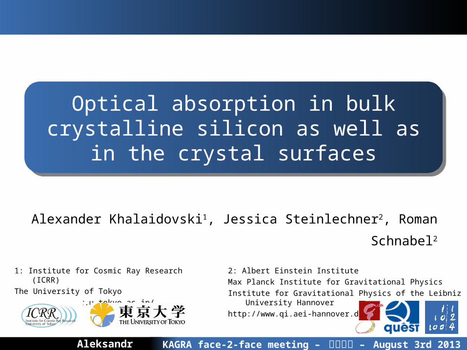
Absorption in bulk crystalline silicon and in the crystal surfacesAleksandr Khalaidovski 1
Alexander Khalaidovski1, Jessica Steinlechner2, Roman Schnabel2
KAGRA face-2-face meeting – 富山大学 – August 3rd 2013
2: Albert Einstein Institute
Max Planck Institute for Gravitational Physics
Institute for Gravitational Physics of the Leibniz University Hannover
http://www.qi.aei-hannover.de
Optical absorption in bulk crystalline silicon as well as in the crystal surfaces
1: Institute for Cosmic Ray Research (ICRR)
The University of Tokyo
http://www.icrr.u-tokyo.ac.jp/
Absorption in bulk crystalline silicon and in the crystal surfacesAleksandr Khalaidovski 2
Outline
Absorption in bulk crystalline silicon and in the crystal surfacesAleksandr Khalaidovski 3
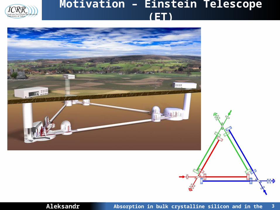
Motivation – Einstein Telescope (ET)
Absorption in bulk crystalline silicon and in the crystal surfacesAleksandr Khalaidovski 4
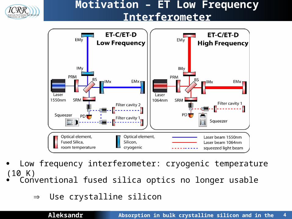
Motivation – ET Low Frequency Interferometer
Low frequency interferometer: cryogenic temperature (10 K)
Conventional fused silica optics no longer usable
Use crystalline silicon
Absorption in bulk crystalline silicon and in the crystal surfacesAleksandr Khalaidovski 5
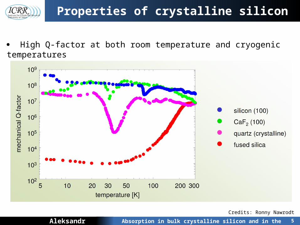
Properties of crystalline silicon
High Q-factor at both room temperature and cryogenic temperatures
Credits: Ronny Nawrodt
Absorption in bulk crystalline silicon and in the crystal surfacesAleksandr Khalaidovski 6
Properties of crystalline silicon
Source: http://www.bit-tech.net/hardware/2010/10/20/global-foundries-gtc-2010/4
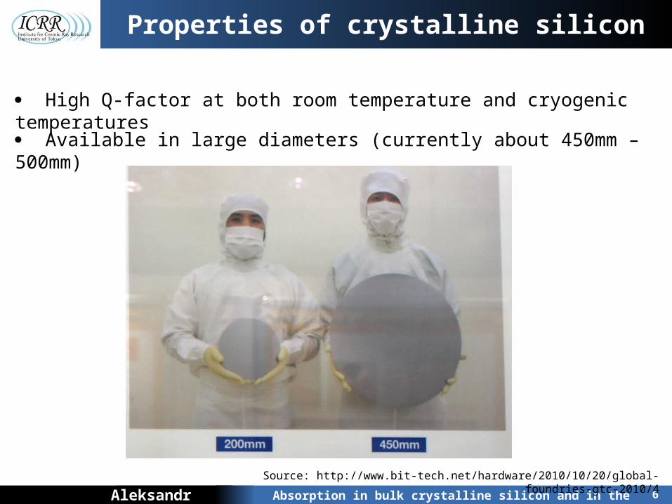
High Q-factor at both room temperature and cryogenic temperatures
Available in large diameters (currently about 450mm – 500mm)
Absorption in bulk crystalline silicon and in the crystal surfacesAleksandr Khalaidovski 7
Properties of crystalline silicon
High Q-factor at both room temperature and cryogenic temperatures
Available in large diameters (currently about 450mm – 500mm)
Completely opaque at 1064 nm, but ...
Absorption in bulk crystalline silicon and in the crystal surfacesAleksandr Khalaidovski 8
Properties of crystalline silicon
?
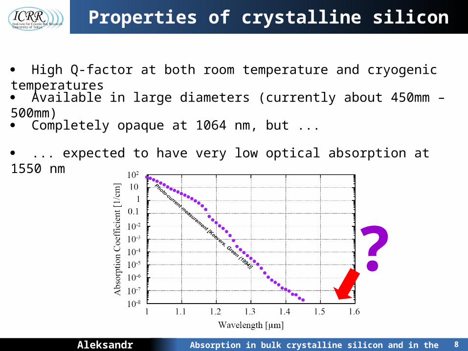
High Q-factor at both room temperature and cryogenic temperatures
Available in large diameters (currently about 450mm – 500mm)
Completely opaque at 1064 nm, but ...
... expected to have very low optical absorption at 1550 nm
Absorption in bulk crystalline silicon and in the crystal surfacesAleksandr Khalaidovski 9
Properties of crystalline silicon
High Q-factor at both room temperature and cryogenic temperatures
Available in large diameters (currently about 450mm – 500mm)
Completely opaque at 1064 nm, but ...
... expected to have very low optical absorption at 1550 nm
currently chosen as candidate material for ET-LF test masses
Absorption in bulk crystalline silicon and in the crystal surfacesAleksandr Khalaidovski 10
Properties of crystalline silicon
High Q-factor at both room temperature and cryogenic temperatures
Available in large diameters (currently about 450mm – 500mm)
Completely opaque at 1064 nm, but ...
... expected to have very low optical absorption at 1550 nm
currently chosen as candidate material for ET-LF test masses
we need to confirm low optical absorption at RT and CT
Absorption in bulk crystalline silicon and in the crystal surfacesAleksandr Khalaidovski 11
Optical absorption measurementsat the AEI Hannover
Absorption in bulk crystalline silicon and in the crystal surfacesAleksandr Khalaidovski 12
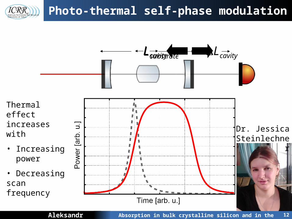
Photo-thermal self-phase modulation
cavityL cavityLsubstrateL
Thermal effect increases with
• Increasing power
• Decreasing scan frequency
Dr. Jessica Steinlechner
Absorption in bulk crystalline silicon and in the crystal surfacesAleksandr Khalaidovski 13
Photo-thermal self-phase modulation
Absorption leads to a heating of the analyzed substrate and thus (for a sum of the thermo-refractive index dn/dT and the thermal expansion coefficient > 0 ) to a thermally induced optical expansion.
When the substrate is placed in an optical cavity and the cavity length is scanned, this thermal expansion affects the detected cavity resonance peaks in a different way for an increase and a decrease of the cavity length.
An external increase of the cavity length and the thermally-induced expansion act in the same direction, resulting in a faster scan over the resonance and thus in a narrowing of the resonance peak.
In contrast, an external cavity length decrease and the thermally-induced expansion partly compensate. As a result, the scan over the resonance is effectively slower, leading to a broader resonance peak.
Absorption in bulk crystalline silicon and in the crystal surfacesAleksandr Khalaidovski 14
Photo-thermal self-phase modulation
Suitable to measure absorption in bulk and coatings
High sensitivity (sub-ppm), small error bars
Does not require high laser power
Requires a cavity setup around the sample
(can be the sample itself with dielectric coatings)
Advantages
Drawbacks
Thermal effect visible not at all laser powers
Absorption in bulk crystalline silicon and in the crystal surfacesAleksandr Khalaidovski 15
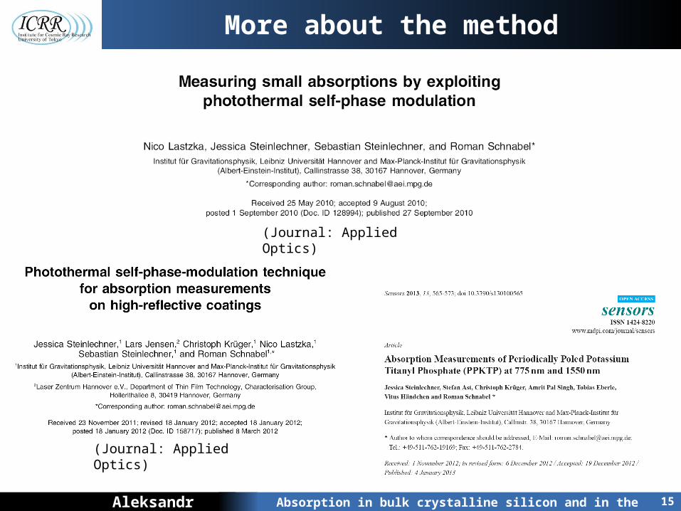
More about the method
(Journal: Applied Optics)
(Journal: Applied Optics)
Absorption in bulk crystalline silicon and in the crystal surfacesAleksandr Khalaidovski 16
Silicon absorption at 1550 nm-
measurement at a fixed optical power
Absorption in bulk crystalline silicon and in the crystal surfacesAleksandr Khalaidovski 17
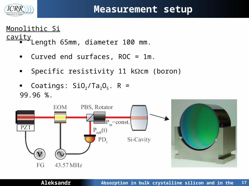
Measurement setup
Length 65mm, diameter 100 mm.
Curved end surfaces, ROC = 1m.
Specific resistivity 11 kcm (boron)
Monolithic Si cavity
Coatings: SiO2/Ta2O5. R = 99.96 %.
Absorption in bulk crystalline silicon and in the crystal surfacesAleksandr Khalaidovski 18
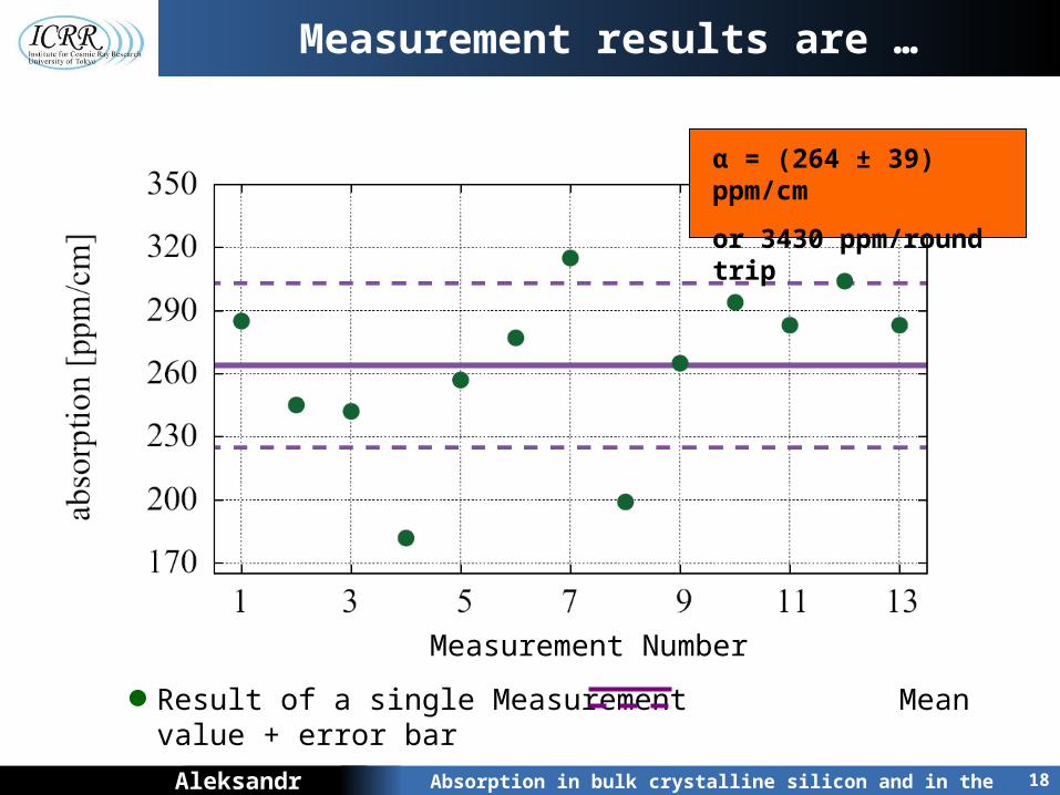
Measurement results are …
Measurement Number
Result of a single Measurement Mean value + error bar
α = (264 ± 39) ppm/cm
or 3430 ppm/round trip
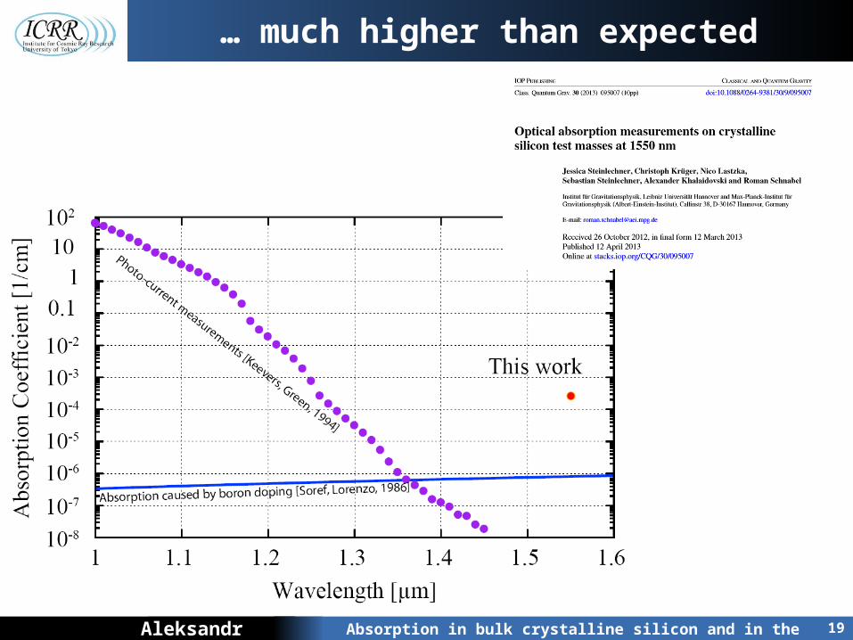
Absorption in bulk crystalline silicon and in the crystal surfacesAleksandr Khalaidovski 19
… much higher than expected
Absorption in bulk crystalline silicon and in the crystal surfacesAleksandr Khalaidovski 20
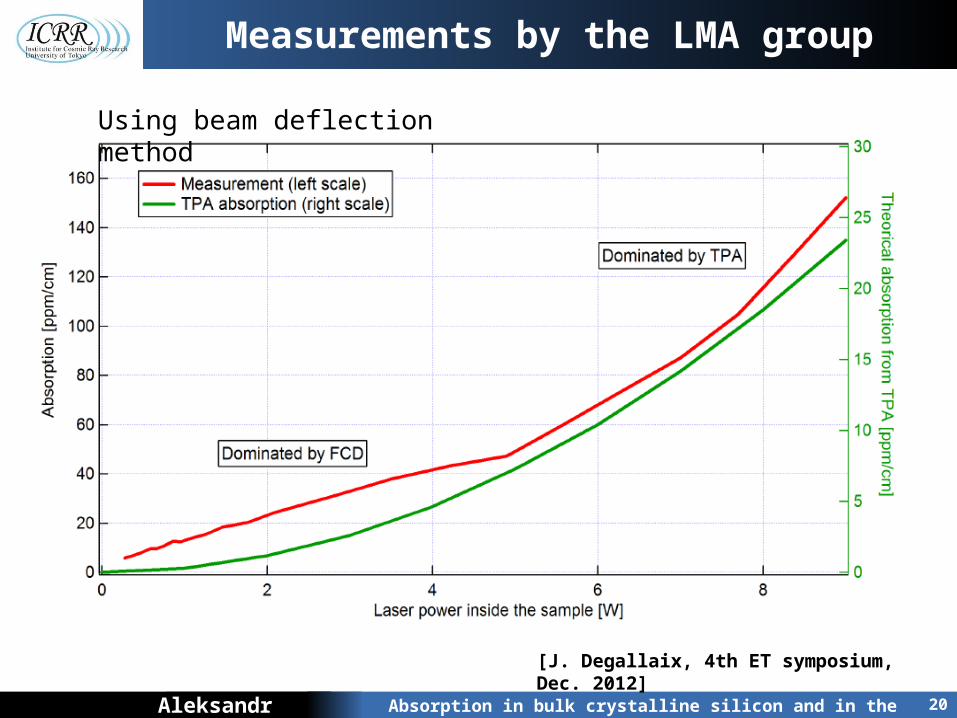
[J. Degallaix, 4th ET symposium, Dec. 2012]
Measurements by the LMA group
Using beam deflection method
Absorption in bulk crystalline silicon and in the crystal surfacesAleksandr Khalaidovski 21
Silicon absorption at 1550 nm-
power-dependent measurements
Absorption in bulk crystalline silicon and in the crystal surfacesAleksandr Khalaidovski 22
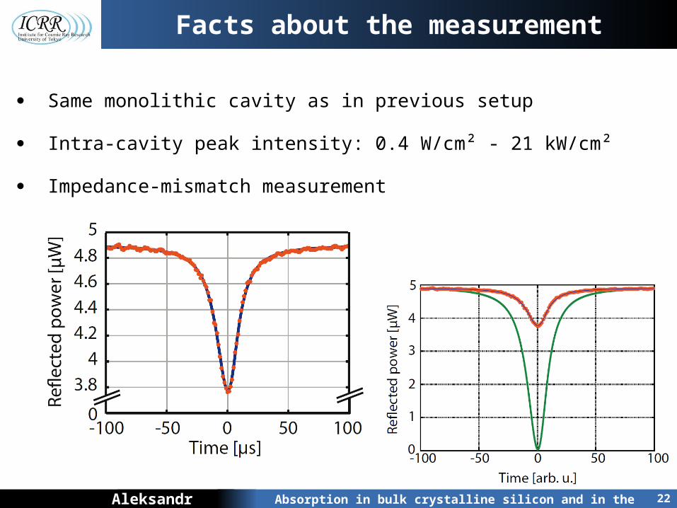
Facts about the measurement
Same monolithic cavity as in previous setup
Intra-cavity peak intensity: 0.4 W/cm² - 21 kW/cm²
Impedance-mismatch measurement
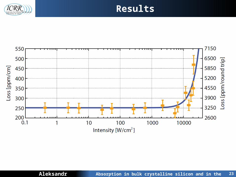
Absorption in bulk crystalline silicon and in the crystal surfacesAleksandr Khalaidovski 23
Results
Absorption in bulk crystalline silicon and in the crystal surfacesAleksandr Khalaidovski 24
Discussion
Results by Degallaix et al. qualitatively confirmed
Reason: probably two-photon absorption, quantitative analysis in progress
I) Non-linear dependence of absorption on optical intensity
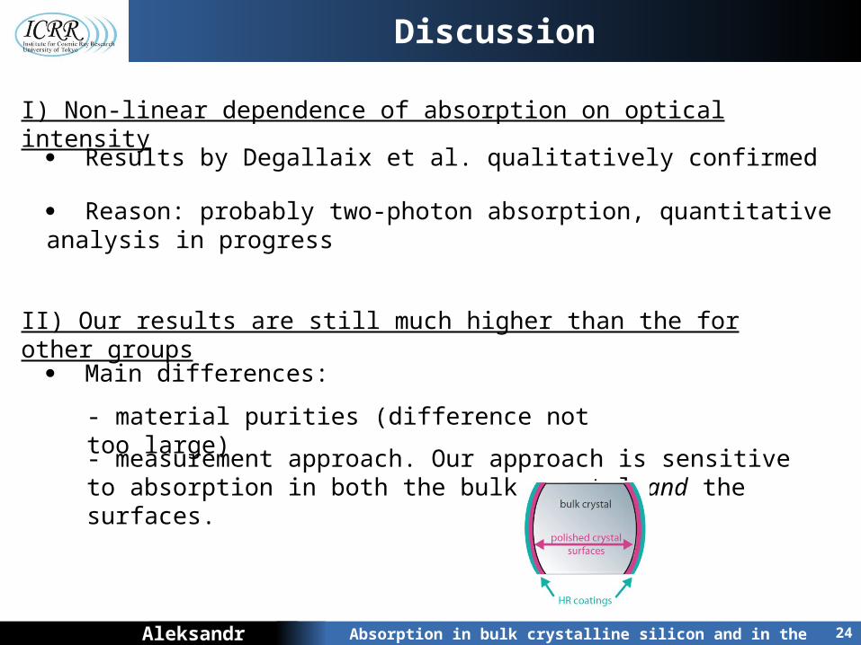
II) Our results are still much higher than the for other groups
Main differences:
- material purities (difference not too large)
- measurement approach. Our approach is sensitive to absorption in both the bulk crystal and the surfaces.
Absorption in bulk crystalline silicon and in the crystal surfacesAleksandr Khalaidovski 25
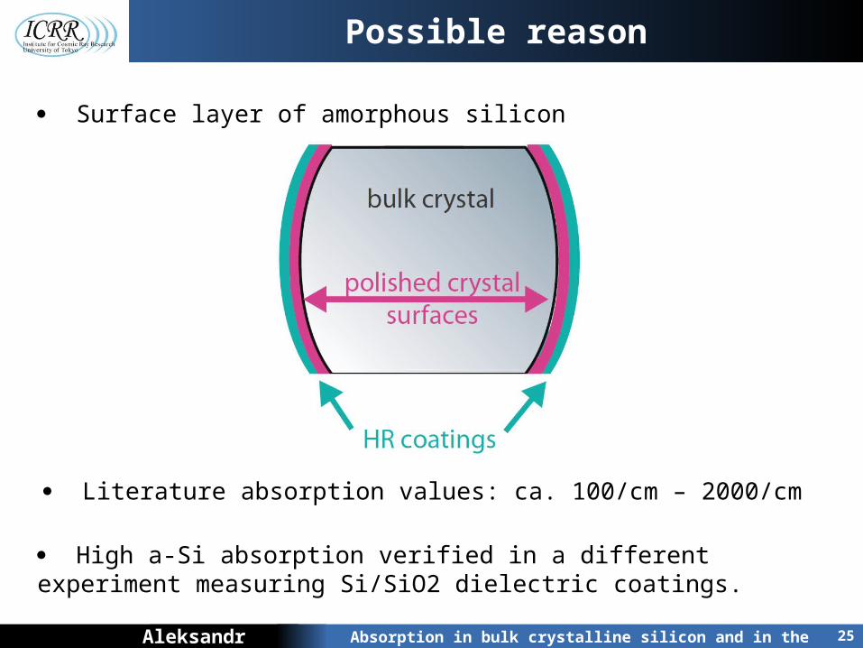
Possible reason
Surface layer of amorphous silicon
Literature absorption values: ca. 100/cm – 2000/cm
High a-Si absorption verified in a different experiment measuring Si/SiO2 dielectric coatings.
Absorption in bulk crystalline silicon and in the crystal surfacesAleksandr Khalaidovski 26
Possible implications
Absorption contribution of about 800 ppm per surface transmission
Absorbed laser power needs to be extracted through the suspensions
1600 ppm for transmission through input test mass (ITM)
Absorption in bulk crystalline silicon and in the crystal surfacesAleksandr Khalaidovski 27
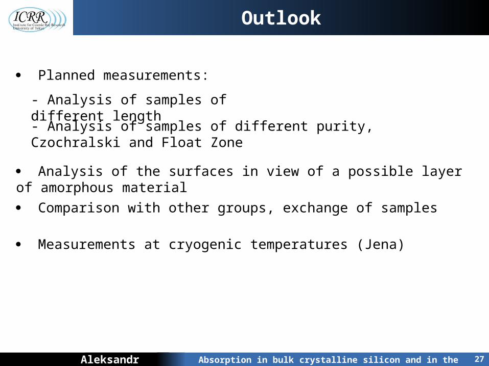
Outlook
Planned measurements:
Analysis of the surfaces in view of a possible layer of amorphous material
- Analysis of samples of different length
- Analysis of samples of different purity, Czochralski and Float Zone
Comparison with other groups, exchange of samples
Measurements at cryogenic temperatures (Jena)
Absorption in bulk crystalline silicon and in the crystal surfacesAleksandr Khalaidovski 28
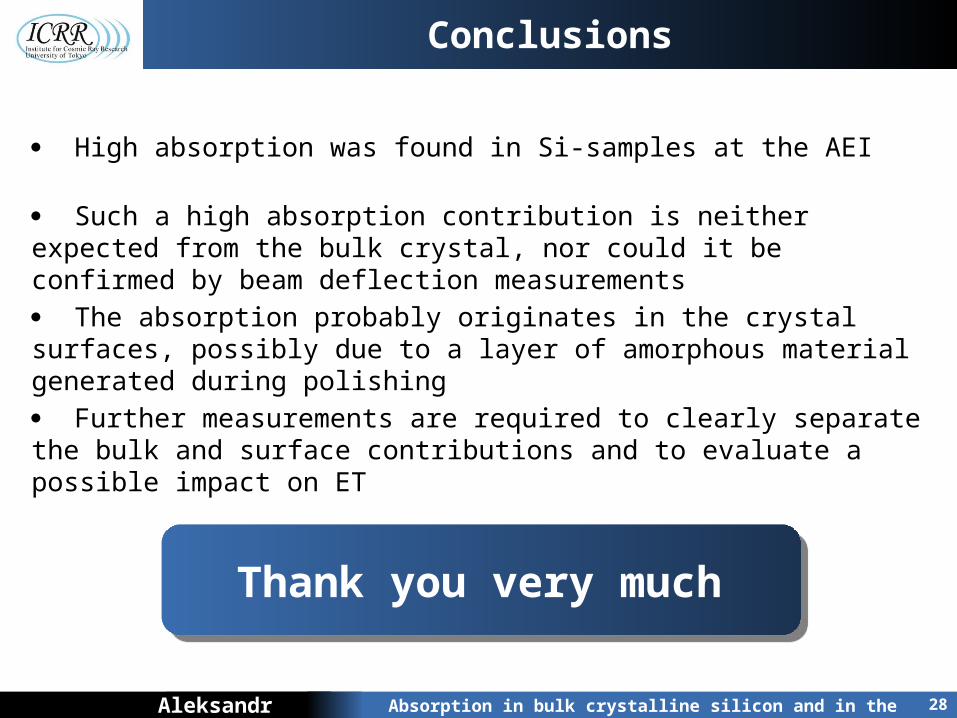
Conclusions
High absorption was found in Si-samples at the AEI
Such a high absorption contribution is neither expected from the bulk crystal, nor could it be confirmed by beam deflection measurements
The absorption probably originates in the crystal surfaces, possibly due to a layer of amorphous material generated during polishing
Further measurements are required to clearly separate the bulk and surface contributions and to evaluate a possible impact on ET
Thank you very much
Absorption in bulk crystalline silicon and in the crystal surfacesAleksandr Khalaidovski 29
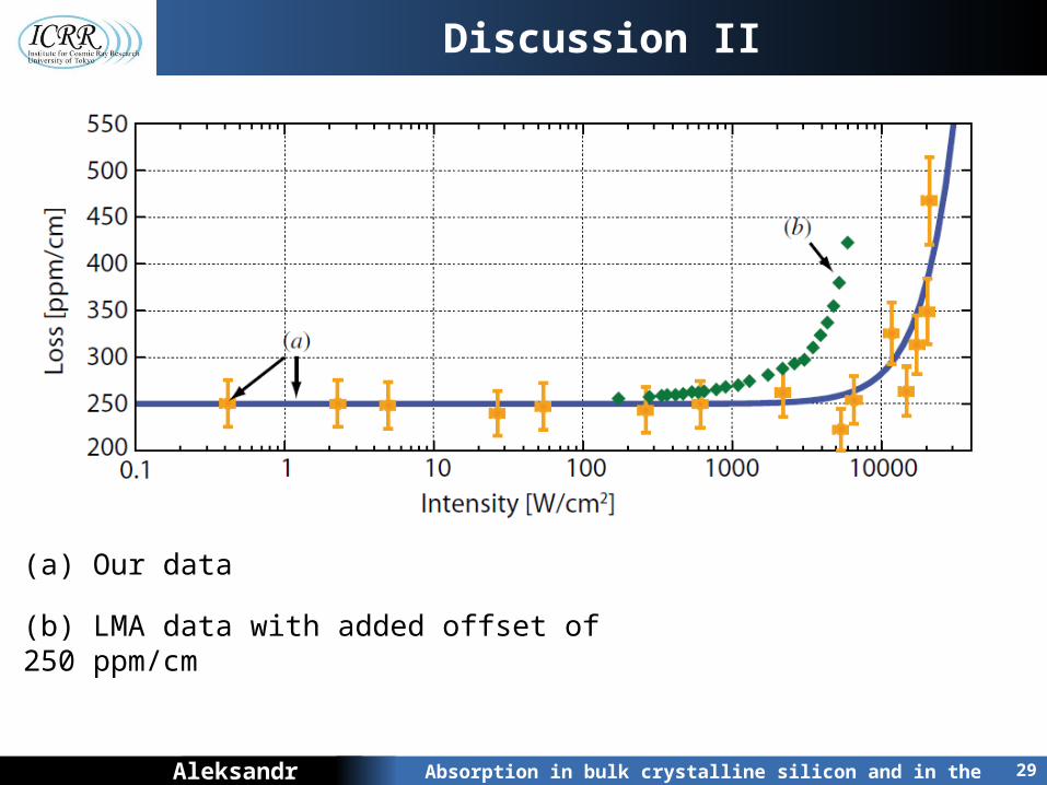
Discussion II
(a) Our data
(b) LMA data with added offset of 250 ppm/cm
Absorption in bulk crystalline silicon and in the crystal surfacesAleksandr Khalaidovski 30
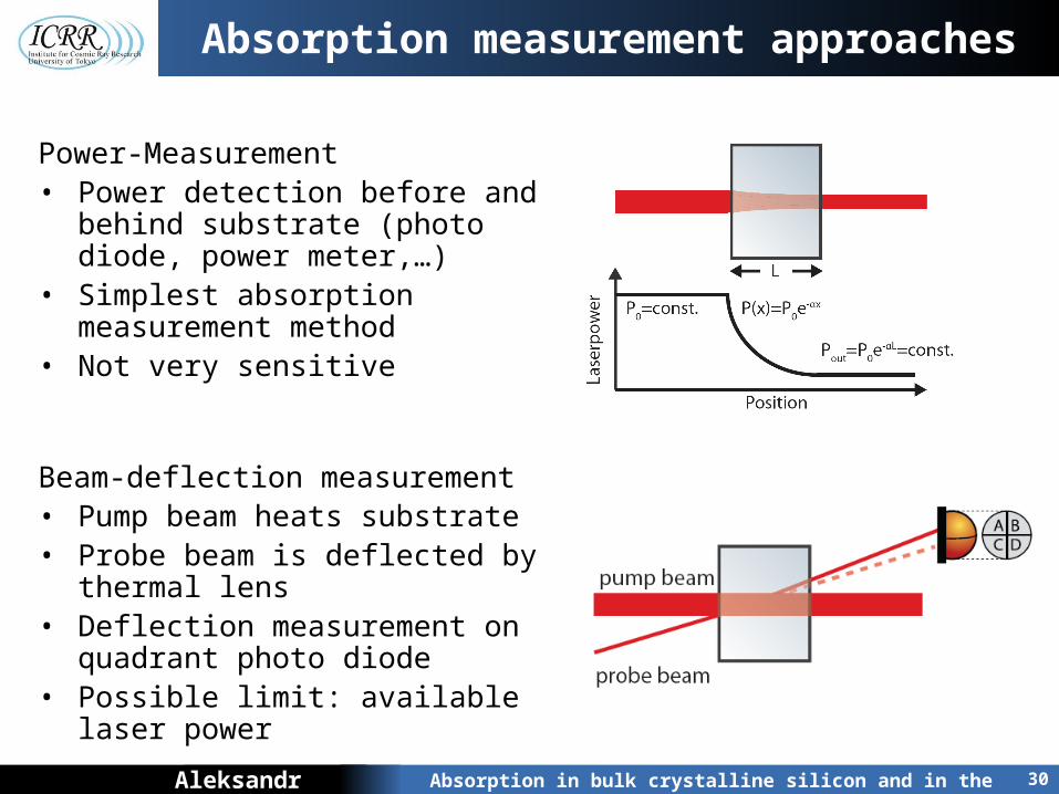
Absorption measurement approaches
Power-Measurement• Power detection before and behind
substrate (photo diode, power meter,…)
• Simplest absorption measurement method
• Not very sensitive
Beam-deflection measurement• Pump beam heats substrate• Probe beam is deflected by thermal
lens• Deflection measurement on
quadrant photo diode• Possible limit: available laser power