Embed Size (px)
Citation preview

THE 2920 ANALOG SIGNAL PROCESSOR DESIGN HANDBOOK
AUGUST 1980

Intel Corporation makes no warranty for the use of its products and assumes no responsibility for any errors which may appear in this document nor does it make a commitment to update the information contained herein.
Intel software products are copyrighted by and shall remain the property of Intel Corporation. Use, duplication or disclosure is subject to restrictions stated in Intel's software license, or as defined in ASPR 7-104.9 (a) (9). Intel Corporation assumes no responsibility for the use of any circuitry other than circuitry embodied in an Intel product. No other circuit patent licenses are implied.
No part of this document may be copied or reproduced in any form or by any means without the prior written consent of Intel Corporation.
The following are trademarks of Intel Corporation and may only be used to identify Intel products:
BXP Intelevision CREDIT Intellec i iSBC ICE iSBX ICS Library Manager im MCS Insite Megachassis Intel Micromap
MULTIBUS· MULTIMODULE PROMPT Promware RMX UPI ,",Scope
and the combinations of ICE, iCS, iSBC, MCS or RMX and a numerical suffix.
MDS is an ordering code only and is not used as a product name or trademark. MDS® is a registered trademark of Mohawk Data Sciences Corporation.
"MULTIBUS is a patented Intel bus.
Additional copies of this manual or other Intel literature may be obtained from:
Literature Department Intel Corporation 3065 Bowers Avenue Santa Clara, CA 95051
© INTELCORPORATION,1980 AFN-01300A-1
TABLE OF CONTENTS
1.0 INTRODUCTION AND TERMINOLOGY 1.1 The 2920 Signal Processor ............................................................. 1-1 1.2 Typical 2920 Design Sequence ......................................................... 1-2 1.3 Benefits of the 2920 Signal Processor Approach ......................................... 1-4
1.3.1 2920 Device Benefits ............................................................ 1-4 1.3.2 Deveiopment-Support-Tool Benefits ............................................. 1-4
2.0 SAM PLED DATA SYSTEMS 2.1 Elements of a Digital Sampled Data System ............................................. 2-1 2.2 Effects of Sampling ................................................................... 2-2
2.2.1 Aliasing Noise .................................................................. 2-3 2.2.2 Signal Reconstruction Distortion ................................................. 2-4 2.2.3 Jitter Noise ..................................................................... 2-5 2.2.4 Quantization Noise .............................................................. 2-6
3.0 THE 2920 SIGNAL PROCESSOR 3.1 Device Operation ................. . . . . . . . . . . . . . . . . . . . . . . . . . . . . . . . . . . . . . . . . . . . . . . . . . . .. 3-1
3.1.1 Overview of the 2920 ............................................................. 3-1 3.1.2 Analog Operations .............................................................. 3-2 3.1.3 DigitalOperations ............................................................... 3-2
3.2 A Closer Look at the Functional Elements ............................................... 3-2 3.2.1 EPROM Section ................................................................. 3-2 3.2.2 Arithmetic Unit and Memory ..................................................... 3-3 3.2.3 The Analog Section ............................................................. 3-7
3.3 Basic 2920 Performance Parameters and Limits ........................................ 3-10
4.0 BUILDING BLOCK FUNCTIONS-FOUNDATION OF DESIGN 4.1 Arithmetic Building Blocks ............................................................. 4-1
4.1.1 Elementary Arithmetic ........................................................... 4-1 4.1.2 Multiplication by a Constant ...................................................... 4-1 4.1.3 Multiplication by a Variable ...................................................... 4-3 4.1.4 Division by a Variable ............................................................ 4-5
4.2 Realizing Relaxation Oscillators ........................................................ 4-6 4.2.1 Reset Technique for Relaxation Oscillator ........................................ 4-6 4.2.2 Overflow Technique for Relaxation Oscillator ..................................... 4-7
4.3 Voltage Controlled Oscillators (VCO's) ................................................. 4-7 4.4 Oscillators Based on Unstable Second-Order Section ................................... 4-8 4.5 Gain Controlled Oscillator ............................................................. 4-8 4.6 Realization of Non-Linear Functions .................................................... 4-9
4.6.1 Simulation of Rectifiers .......................................................... 4-9 4.6.2 Simulation of Limiters ........................................................... 4-9
5.0 SUMMARY OF FILTER CHARACTERISTICS 5.1 Characteristics of "Ideal" Filters ....................................................... 5-1
5.1.1 The Rectangular Filter ........................................................... 5-1 5.2 Minimum Phase Filters ................................................................ 5-2
5.2.1 Butterworth Filters .............................................................. 5-2 5.2.2 Chebyshev Filters ............................................................... 5-2 5.2.3 Elliptic Function Filters .......................................................... 5-2 5.2.4 Bessel and Gaussian Filters ..................................................... 5-3 5.2.5 Transitional Gaussianl Butterworth Filters ........................................ 5-3 5.2.6 Other Minimum Phase Filters .................................................... 5-3 5.2.7 Comparison of Minimum Phase Filters ...............................•............ 5-3
TABLE OF CONTENTS
5.3 Non-Minimum Phase and Allpass Networks ............................................. 5-4 5.4 Review of Analog Filter Characteristics ................................................. 5-4
5.4.1 Effects of Pole/Zero Location on Filter Parameters ................................ 5-4 5.4.2 Transient Response and Selectivity ................... , .......................... 5-5
5.5 Digital Filters ......................................................................... 5-6 5.2.1 IIR Filters ....................................................................... 5-7 5.5.2 FIR Filters ...................................................................... 5-7 5.5.3 Canonical Forms of Digital Filters ................................................ 5-7 5.5.4 Matched Z Transform ............................................................ 5-9 5.5.5 Bi linear Transform ............................................................. 5-10
5.6 Implementing Filters with the 2920 ..................................................... 5-11 5.6.1 Simulating Single Real Poles .................................................... 5-12 5.6.2 Simulating Complex Conjugate Pole Pairs ....................................... 5-13 5.6.3 Realizing Zeros in Basic Filter Sections .......................................... 5-14 5.6.4 Complex Conjugate Zero Pairs .................................................. 5-14 5.6.5 Some Practical Considerations .................................................. 5-15 5.6.6 Very Low Frequency Filters ..................................................... 5-16 5.6.7 Filters at a Multiple of the Sampling Rate ......................................... 5-17 5.6.8 Other Filter Structures .......................................................... 5-17
6.0 ADVANCED TECHNIQUES 6.1 Time VarIable Filters .................................................................. 6-1 6.2 Noise Generation with the 2920 ......................................................... 6-4 6.3 Digitallnput/Output .......................... ,......................................... 6-4
7.0 APPLICATION EXAMPLES 7.1 Sweeping Local Oscillator ............................................................. 7-1 7.2 Piecewise Linear Logarithmic Amplifier ................................................ 7-2 7.3 Digital Filter .......................................................................... 7-5 7.4 The 2920 as a Spectrum Analyzer ....................................................... 7-7
7.4.1 Description of Spectrum Analyzer ................................................ 7-7 7.4.2 Block Diagram Description ....................................................... 7-7 7.4.3 Sampled Data System Considerations ............................................ 7-9 7.4.4 Complete Spectrum Analyzer Assembly Listing .................................. 7-10
8.0 DESIGN CONSIDERATIONS 8.1 2920 Debugging Procedures ........................................................... 8-1 8.2 Description of Application Breadboard ................................................. 8-2
8.2.1 Layout Considerations .......................................................... 8-2 8.2.2 Parts List ....................................................................... 8-5
9.0 2920 SUPPORT TOOLS 9.1 The Assembler ....................................................................... 9-1 9.2 The Simulator ......................................................................... 9-1
9.2.1 Concept of Simulation, Testing and Debugging .................................... 9-1 9.2.2 Modes of Operation ............................................................. 9-2 9.2.3 A Generalized Simulation Session ................................................ 9-3
9.3 The 2920 Signal Processing Applications Software/Compiler ............................. 9-3
APPENDIX
REFERENCES
ii

Introduction and Terminology 1

CHAPTER 1 INTRODUCTION AND TERMINOLOGY
1.0 INTRODUCTION AND TERMINOLOGY
This handbook provides the background review and design examples that will help the reader to understand analog signal processing applications using INTEL's digital signal processing system, the 2920. The 2920 uses digital sampled data techniques to implement continuous analog functions. In another words, analog signal processing can now be performed with digital signal processing techniques using the 2920.
Before looking at digital signal processing, it is useful to clarify the distinctions between signal processing and digital processing. Signal processing deals with continuous analog waveforms, whereas digital processing operates on data that are represented in a digital form. Digital signill processing would then be the operation on digital representation of continuous signals.
Digital signal processing, in the most general sense, means creating, altering, or detecting continuous signals, using digital rather than analog or electromechanical implementations. Furthermore, signal processing can be distinguished from data processing in that the former implies that real-time processing is needed. Data processing, however, implies the manipulation of data (which mayor may not represent an action occurring presently) in a batch or off-line manner, where the need for the result is not a function of real-time.
Most digital microprocessors are designed for data processing, not for high-speed complex signal processing. The industry-standard 8080/8085 microprocessor system can operate as a signal processor at frequencies to only a few hundred hertz, and will require mUltiple chips with a separate analog/digital conversion system and I/O circuitry.
By contrast, general signal processing frequencies are in the kilohertz range (thousands of cycles per second). Many signals, such as speech, heartbeat, and seismic waveforms are complex, and in many cases, multiple signals must be processed in parallel. Because of different requirements for signal processing, a general purpose microprocessor is not well suited for signal processing applications. A different processor architecture is required to implement signal processing algorithms.
1-1
1.1 The 2920 Signal Processor
The 2920 Signal Processor is a single chip microcomputer designed especially to process real-time analog signals. The 2920 has on-board program memory, scratchpad memory, D/ A circuitry, A/D circuitry, digital processor, and I/O circuitry. It is more than a single device, but is a complete digital sampled data system. The architecture and instruction set was developed to perform precise, high speed signal processing. The processor executes its programs at typically 13,000 times a second when used with a 10 MHz clock and full program memory. Each execution (1 pass of the 2920 program memory) can process up to four input signals and up to eight analog output signals. The processing speed allows signals with bandwidths to 5 kilohertz to be processed; shorter programs permit higher bandwidth. Its capabilities in signal processing are diverse and powerful, and include an extremely broad range of applications.
Some of the signal processing functions the 2920 can implement are shown in Table 1-1. It is important to note that these are fundamental building block functions which corresponds to functional blocks in an application block diagram. These are some of the building blocks that can be linked together to implement complex applications. Table 1-2 shows some of the possible application areas for the 2920 Signal Processor.
The 2920 Signal Processor can implement any of the listed functions under program control. Many functions can be realized on the same chip. Interleaving multiple inputs or outputs allows for several independent circuits or a single highly complex one to be implemented. Even higher complexity can be achieved by cascading 2920s. If increased speeds are desirable, several 2920s can be used in serial or parallel to achieve this. In most cases, complete signal processing applications are implemented on a single device.
The 2920 Signal Processor is only part of the solution. Since a large part of the cost in producing a product is the development time needed to design, test, and integrate the new circuit into the final product, the 2920 support package has been developed. It provides the software and hardware necessary to take a design from concept to implementation on the 2920 Signal Processor. This system combines a standard INTEL Intellec Series II microcomputer development system with the signal processing support package (SPS-20) to provide a powerful set of hardware and software support tools. This is described in Chapter 9.

INTRODUCTION AND TERMINOLOGY
Table 1-1. Signal Processing Functions
FILTERING Complex poles and zeros Arbitrary digital filter configurations Multiple parallel or cascaded filter combinations High accuracy and stability
WAVEFORM GENERATION Arbitrary waveforms, e.g., sine, square, triangle, etc. Broad frequency range with high resolution 9-bit amplitude accuracy
NONLINEAR FUNCTIONS Full wave rectifiers Limiters Comparators
~ ANXN
Multiply/Divide EX
PROCESSING Controllable with external signals (analog or digital inputs) Phase locked loops
Adaptive filters MODULATION/DEMODULATION
Amplitude, frequency and phase modulation Continuous or digital, e.g., FM and/or FSK Analog or digital inputs and outputs
Pipeline processing using multiple 2920s
Table 1-2. Broadly Based 2920 Signal Processor Applications Base
TELECOMMUNICATIONS DTMF /MF receivers Modems Tone/cadence generators FSK/PSK mod/demod Adaptive equalizers.
PROCESS CONTROL Transducer linearization Remote feedback control Remote data link Signal conditioning
SIGNAL PROCESSING Waveform generators Correia tors Digital filters Adaptive filters Speech processing Seismic processing Sonar processing Transducer linearization
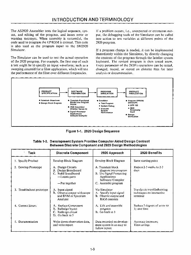
1.2 Typical 2920 Design Sequence
Designing with the 2920 Signal Processor is best thought of in terms of the building block functions it can implement and the application models already available as 2920 routines (see Chapter 7). The designer should COnsider short 2920 assembly language routines as tools which can be combined to achieve the desired system function.
1-2
GUIDANCE AND CONTROL Missile guidance Torpedo guidance Motor control
SPEECH PROCESSING Vocoders Speech analysis Pitch extraction Speech synthesis Speech recognition
TEST AND INSTRUMENTATION Phase locked loops Frequency locked loops Scanning spectrum analyzer Digital filters
INDUSTRIAL AUTOMATION Position and rate control Communication links Servo links
The first operation for the designer is to develop a detailed system block diagram similar to one for a continuous analog design. Each block is then realized in 2920 code and arranged in a suitable sequence. The 2920 Signal Processing Applications Software/Compiler (SP AS-20) can be used interactively to facilitate developing the precise code to meet design constraints. The code can then be assembled as individual functional blocks or as an entire system. Once the functions or system has been assembled, it can be debugged via use of the simulator.
INTRODUCTION AND TERMINOLOGY
The AS2920 Assembler tests the logical sequence, syntax, and editing of the program, and issues error or warning messages. When assembly is successful, the code used to program the EPROM is created. This code is also used as the program input to the SM2920 Simulator.
The Simulator can be used to test the actual operation of the 2920 prograrp. For example, the first step of such a test might be to specify an input waveform; such as a sweeping sinusoid for a filter application, which will test the performance of the filter over different frequencies.
• Establish Objectives • DeSign Block Diagram
• Translate Functional Blocks Into Program Blocks
• 2920 Assembler (Intellec®Senes II)
• Signal Processor Appllcallons Soltware/Compller
If a problem occurs, i.e., unexpected or erroneous output, the debugging tools of the Simulator can be called into action to test variables at different points of the 2920 program.
If a program change is needed, it can be implemented immediately within the Simulator, by directly changing the contents of the program through the Intellec system keyboard. The revised program is then tested anew. Every parameter of the 2920's operations can be tested, changed, traced, or stored on diskette files for later analysis or documentation .
• SimUlator
• Test Program • System Debug
• Evaluate System Performance
• Program EPROM (Intellec®) • UPP 103
• 2920 Personality Card
• DeSign Venllcallon
Figure 1-1. 2920 Design Sequence
Table 1-3. Development System Provides Computer Aided DeSign Contrast Between Discrete Component and 2920 DeSign Methodologies
Task Discrete Component 2920 Approach 2920 Benefits
1. Specify Product Develop Block Diagram Develop Block Diagram Same starting point
2. Develop Prototype A. Design Circuits A. Translate block Reduce 2-3 weeks to 2-3 B. Design Breadboard diagram into program days C. Build Breadboard B. Use Signal Processing
-Locate parts Applications Software/Compiler
-Put together C. Assemble program
3. Troubleshoot prototype A. Input signal Via Simulator Use classic troubleshooting B. Observe output with scope A. Specify input signal techniques on interactive
and DVM or Spectrum B. Observe output and terminal Analyzer RAM contents
4. Correct Errors A. Replace Component A. Edit and assemble Reduce 3 degrees of error to B. Redesign layout program 1; save time C. Redesign circuit B. Go back to 3 D. Go back to 3
5. Documentation Write down observation data, Data recorded on develop- Accuracy increases; and write report ment system in an easy to Time savings
follow report
1-3

INTRODUCTION AND TERMINOLOGY
When the simulation indicates the program is operating to specifications, it can be stored on a diskette. The latest version can then be loaded into the 2920 device for testing in the hardware prototype.
Figure 1-1 outlines the development sequence for a 2920 design. There are several important points to note that makes the 2920 much more efficient for a system design: 1) With the 2920, hardwired analog functions are now
implemented with flexible software, 2) Instead of designing circuits for each of the building
blocks of the block diagram, a sequence of 2920 instructions are used to implement each of the blocks,
3) Instead of building hardware prototypes early in the design phase of the product development, the 2920 uses a computer-aided design and debug package to facilitate design and development, and
4) There is no need for a hardware prototype until such a time that the system has been simulated and found to be completely functional and meets design specifications.
Table 1-3 shows the contrast in design methodologies for a 2920 design and one using analog components. Numerous benefits derive from using the 2920 development system for signal processing design and implementation. The digital methodology, with its unique tools (see Chapters 3 and 9) to aid designing and debugging, helps to: a) standardize the design process, and b) allow for immediate changes. Thus it can c) reduce drastically the time needed for creating new
products or for modifying prior work to fix errors or to add new features.
1.3 Benefits of the 2920 Signal Processor Approach
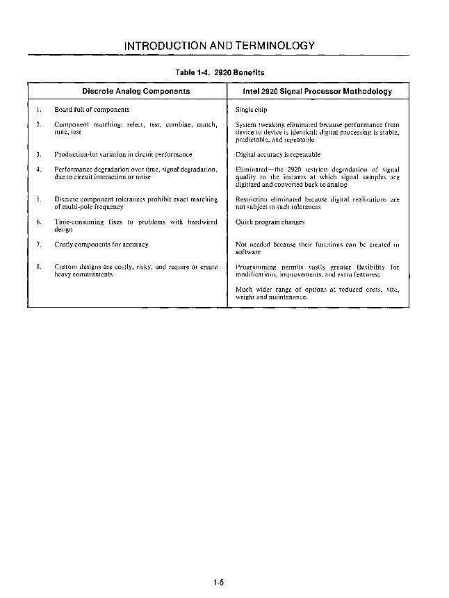
The 2920 is a solution for many signal processing needs. It is a complete system in a single 28-pin package. Along with 2920 are all the design and development tools required to move a product idea into finished product. The 2920 uses a digital sampled data system approach for signal processing applications. The digital sampled data approach brings many attributes to signal processing. Table 1-4 summarizes some of these benefits.
1.3.1 2920 Device Benefits
Lower manufacturing cost for 2920-based products results from a lower part count, improved reliability,
1-4
and the elimination of costly preCiSion components. Also eliminated is the production re-tuning or 'tweaking' so often required in analog systems integration.
The flexibility for rapid design changes in prototypes is a direct result of the 2920's programmability. Alternative designs are readily compared by reprogramming the 2920's EPROM. The re-use of standard debugged program blocks facilitates the creation of alternatives in both existing and future products.
The digital approach provides inherently stable, predictable, and reproducible results. The NMOS integrated circuitry means increased reliability. Conceptual errors or inefficient implementation choices are easily found during debugging and performance evaluation using the 2920 Simulator. The performance you design for is the realized performance.
Savings in long-term product maintenance, support, and enhancement result from the relative ease with which engineering changes are implemented in software. Field maintenance is reduced by digital stability and LSI reliability.
1.3.2 Deveiopment-Support-Tool Benefits
Long term savings in large part are derived from the 2920 support package. The 2920 Signal Processing Applications Software/Compiler (SPAS-20) contains very powerful code generation and macro capabilities, plus graphics and analysis capabilities permitting interactive specification and adjustment of design parameters. Creating usable libraries of macros and signal processing routines means ever increasing productivity due to building on the successes of the past.
The 2920 Assembler creates the actual machine bit patterns to be programmed into the 2920. Its careful error analysis detects problem areas, and the debugging information it provides greatly facilitates design evaluation during simulation.
The 2920 Simulator permits execution of any part of a 2920 program, plus collection of trace data on variables. This tool bears a strong family resemblance to Intel's In-Circuit-Emulators (ICE). The analysis and evaluation capabilities inherent in the 2920 Simulator make possible rapid problem isolation in the field or in the factory. It can also be used to generate revised object code for a quick check on proposed fixes or enhancements. This revised code can be saved and used to program the 2920.
J.
2.
3.
4.
5.
6.
7.
8.
INTRODUCTION AND TERMINOLOGY
Table 1-4. 2920 Benefits
Discrete Analog Components
Board full of components
Component matching: select, test, combine, match, tune, test
Production-lot variation in circuit performance
Performance degradation over time, signal degradation, due to circuit interaction or noise
Discrete component tolerances prohibit exact matching of multi-pole frequency
Time-consuming fixes to problems with hardwired design
Costly components for accuracy
Custom designs are costly, risky, and require or create heavy commitments
1-5
Intel 2920 Signal Processor Methodology
Single chip
System tweaking eliminated because performance from device to device is identical: digital processing is stable, predictable, and repeatable
Digital accuracy is repeatable
Eliminated-the 2920 restricts degradation of signal quality to the instants at which signal samples are digitized and converted back to analog
Restriction eliminated because digital realizations are not subject to such tolerances
Quick program changes
Not needed because their functions can be created in software
Programming permits vastly greater flexibility for modifications, improvements, and extra features;
Much wider range of options at reduced costs, size, weight and maintenance.

Sampled Data Systems 2


CHAPTER 2 SAMPLED DATA SYSTEMS
2:0 SAMPLED DATA SYSTEMS
Sampled data systems can be implemented using either analog or digital processing techniques, or both. Figure 2-1 shows two different types of sampled data systems: sampled analog system and sampled analog/digital system. Examples of sampled analog systems include transversal filters using CCD or bucket brigade shift registers analog weighted-taps and switched capacitor techniques to implement a filter characteristic. The identical systems can also be implemented using digital instead of analog processing. Such systems are referred to as digital sampled data systems. This type of system can be implemented with the 2920 Signal Processor. This chapter will discuss the various elements that comprise a digital sampled data system and also look at the design considerations in representing a continuous analog signal with digital sampled data techniques.
2.1 Elements of a Digital Sampled Data System
The block diagram shown in Figure 2-2 illustrates the basic blocks of a general purpose sampled data system using a digital signal processor. In this configuration it is assumed that both the input and output signals are analog. This is not a necessary condition since digital signals can be considered a special type of analog signals and processed accordingly. Elements of the block diagram are discussed below.
The system in Figure 2-2 operates on the input analog signal using the indicated components in sequence:
• Anti-Aliasing Filter-This filter is used to bandlimit the incoming analog signal prior to sampling; thus a continuous analog filter is used. This minimizes possible distortion terms (aliasing noise) which could arise from signal frequencies that are too high relative to the sample rate (Section 2-2).
• Input Sample and Hold (S&H)-The filtered input signal is then sampled at a fixed rate determined by the digital processor. Each resulting sampled amplitude is held long enough for subsequent processing (such as analog-to-digital conversion).
2-1
Analog-to-Digital Converter (A/D)-The held analog voltage is converted to a digital word. This digital word then represents the sampled input signal voltage. (Since the processor must operate on individual digital words, it is necessary to characterize the continuous analog input signal by discrete digital words which retain the information of the original signal.)
• Digital Processor-Each digitized sample is now processed by the digital processor, which has been programmed to perform a predetermined algorithm. Typically, a general microprocessor can be programmed to perform any funciton, but the resulting execution time is too limiting for most analog applications. The 2920 eliminates this problem because its architecture is configured to take advantage of serial repetitive signal processing, while at the same time preserving many of the advantages of the general purpose microprocessor.
Digital-to-Analog Converter (D/ A)-The processed digital words are converted back to analog using the D/ A. Again, the analog signal is approximated by discrete amplitude levels (as in the A/D). In addition, the D/ A sampled output weights the signal output in the frequency domain by sin(x)/x, thereby causing some signal distortion (Section 2-2).
• Output Sample-and-Hold (S&H)-One method of reducing the output frequency distortion is to widen the sin(x)/x rolloff by resampling the output signal using a very narrow sample width. The S&H takes the D/ A held output and res am pies it with narrow pulses. Another use of an output S&H is to store values when several outputs are multiplexed during a single sample period.
• Reconstruction Filter-Since the desired output signal is a continuous representation of the processed input signal, it is necessary to remove high frequency components resulting from the D/ A or sample-and-hold outputs. This, in effect, smooths the analog output from sample to sample. A lowpass filter is used to perform the signal "reconstruction". This filter can also be used to compensate for the sin(x)/x frequency rolloff of the D/ A or S&H (Section 2-2).

SAMPLED DATA SYSTEMS
C) SAMPLED ANALOG/DIGITAL SYSTEM
Figure 2·1. Sampled Data System
Figure 2·2. Elements of a Sampled Data System
2.2 Effects of Sampling
Assuming an input spectrum F(jw) and a sampling frequency fs, the output spectrum for square-topped sampling Fst (jw) is found to be
FST (jw) =.2.... sin (wtl2) T wtl2
L F [j(w-nws)] n=-oo
From this equation, the gain is a continuous function of frequency defined by ~ SIn Jt~y2) where T is the sample pulse width, t is time, T the sample period, and w the frequency in radians per second.
The time-and-frequency-domain plots for the squaretopped sampled signals are shown in Figure 2-3. Figure 2-3a and 2-3b show the signal before and after sampling. The corresponding spectra are shown in Figure 2-3c and 2-3d respectively. Figure 2-3d is a plot of the above equations where multiple spectra are formed around mUltiples of the sample frequency. As long as
2-2
the adjacent spectra do not overlay excessively (aliasing distortion), the continuous signal can be represented by discrete samples at that sampling frequency.
The quality of representation of a continuous signal by the sampled and digitized signal is determined by several factors: a) sampling rate b) sampling pulse width c) sampling stability and d) digitizing accuracy. The corresponding distortion terms are: a) aliasing noise b) signal reconstruction noise c) jitter noise and d) quantization noise respectively. These four factors can cause unacceptable distortion if they are not chosen properly.
By properly designing the sampled data system, these distortion or noise terms can be made insignificantly small, so that the sampled data system closely represents the analog equivalent system.
The sampled data system implementation will have the added advantages of digital processing and software flexibility. The following sections will discuss these sources of imprecision.
a lnput~slgnal waveform
b Square-topped sampled signal
FREQUENCY
c Input-signal spectrum
{T--;;;;t2 D.. - __
~ ::E ..: ~.... -- .... --
t'""""t •
d Square-topped sampled-signal spectrum
Figure 2·3. Analysis of Sampled Signal
SAMPLED DATA SYSTEMS
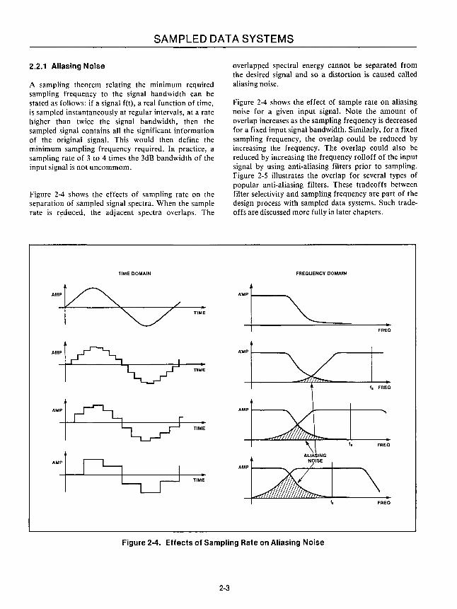
2.2.1 Aliasing Noise
A sampling theorem relating the minimum required sampling frequency to the signal bandwidth can be stated as follows: if a signal f(t), a real function of time, is sampled instantaneously at regular intervals, at a rate higher than twice the signal bandwidth, then the sampled signal contains all the significant information of the original signal. This would then define the minimum sampling frequency required. In practice, a sampling rate of 3 to 4 times the 3dB bandwidth of the input signal is not uncommom.
Figure 2-4 shows the effects of sampling rate on the separation of sampled signal spectra. When the sample rate is r~duced, the adjacent spectra overlaps. The
TIME DOMAIN
AM'~'C7L TIME
A·'I~LLL:/ TIME
A·'I~ TIME
A.') ~ TIME
overlapped spectral energy cannot be separated from the desired signal and so a distortion is caused called aliasing noise.
Figure 2-4 shows the effect of sample rate on aliasing noise for a given input signal. Note the amount of overlap increases as the sampling frequency is decreased for a fixed input signal bandwidth. Similarly, for a fixed sampling frequency, the overlap could be reduced by increasing the frequency. The overlap couJd also be reduced by increasing the frequency rolloff of the input signal by using anti-aliasing filters prior to sampling. Figure 2-5 illustrates the overlap for several types of popular anti-aliasing filters. These tradeoffs between filter selectivity and sampling frequency are part of the design process with sampled data systems. Such tradeoffs are discussed more fully in later chapters.
FREQUENCY DOMAIN
A.' I ~ FREQ
A.' I f. FREQ
AMP
f. FREQ
A·'IZ!. \ •
FREQ
Figure 2-4. Effects of Sampling Rate on Aliasing Noise
2-3
SAM PLED DATA SYSTEMS
10
20
30
40
1/21s
FREQUENCY
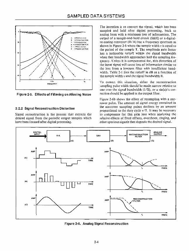
o 0 3 POLE BWRTH .0 3POLEO 3dBTCH
A 0 5 POLE BWRTH
.. 0 5POLEO 3dBTCH
c 0 7 POLE BWRTH
• 0 7POLEO 3dBTCH
Is
Figure 2·5. Effects of Filtering on Aliasing Noise
2.2.2 Signal Reconstruction Distortion
Signal reconstruction is the process that extracts the desired signal from the periodic output samples which have been formed after digital processing.
DIGITAL INPUT
D/A
The intention is to convert the signal, which has been sampled and held after digital processing, back to analog form with a minimum loss of information. The output of a sample-and-hold circuit (S&H) or a digitalto-analog converter (DI A) has a frequency spectrum as shown in Figure 2-6 where the sample width T is equal to the period of the sample T. The amplitude gain factor has a noticeable rolloff within the signal bandwidth when that bandwidth approaches half the sampling frequency. Unless it is compensated for, this distortion of the input signal will cause loss of information similar to the loss from a lowpass filter with insufficient bandwidth. Table 2-1 lists the rolloff in dB as a function of the sample width T and the signal bandwidth B.
To correct this situation, either the reconstruction sampling pulse width should be made narrow relative to one over the signal bandwidth (1/B), or a sin(x)/x correction should be applied in the output filter.
Figure 2-6b shows the effect of resampling with a narrower pulse. The amount of signal energy contained in the narrower sampling pulses declines by an amount proportional to the duty cycle TIT. It may be necessary to compensate for this gain loss when analyzing the relative effects of fixed offsets, overshoot, ringing, and other spurious signals that degrade the desired signal.
ANALOG OUTPUT
·1 L S&H ~ ___ ----I,",~I RECO~~L~~~CTION '-_____ -" (8) ""--_____ .... (C)
.;
(A) AM'I~ LLJ
.. TIME
AMP
I. FREO
AM'I n n Dr-. (8) DODD TIME AM' t ~" I. FREO
AM'p~// (C)
------- RECONSTRUCTION AMP ,
,/FILTER
, " "
I. FREO
.. TIME
Figure 2-6. Analog Signal Reconstruction
2-4
SAMPLED DATA SYSTEMS
When the data samples have been established, they are passed through a reconstruction lowpass filter whose primary purpose is to remove the higher-frequency spectra caused by the output sampling (Figure 2-6c). It can also help shape the amplitude and phase response of the output network.
Table 2-1. Reconstruction Distortion Due to Sample Pulse Width
BT -20 log
sin nBT ---
nBT
dB
0.1 0.14 0.2 0.58 0.3 1.32 0.4 2.40 0.5 3.92 0.6 5.96 0.7 8.70 0.8 12.60 0.9 19.3 1.0 00
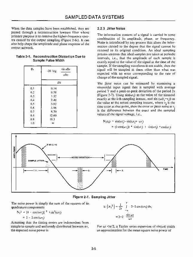
2.2.3 Jitter Noise
The information content of a signal is carried in some combination of its amplitude, phase, or frequency. Noise is introduced by any process that alters the information carried to the degree that the signal cannot be restored to its original condition. An ideal sampling process assumes that ideal samples are taken at periodic intervals, i.e., that the amplitude of each sample is exactly equal to the value of the signal at the time of the sample. If the sampling waveform is not stable, then the signal will be sampled at times other than what was expected with an error corresponding to the rate of change of the sampled signal.
The jitter noise can be estimated by examining a sinusoidal input signal that is sampled with average period T and a peak-to-peak deviation of the period 2T (Figure 2-7). Using sin(wti) as the value of the sinusoid exactly at the i-th sampling instant, and sin (W(tj+Tj» as the value at the actual sampling instant, where Ti is the time error at that point, then the error or jitter noise at ti is the difference between the exact and the sampled values of the signal voltage, i.e.,
NJ(t.) = sin(wtl) - sir,(wti+ WTI)
= (l-COS(WT) * sin(wt) + sin(wTi) * cos(wt)
11-- } .... I-----NOISE VARIATION---__
SAMPLE JITTER~::II -11111111 11111111
I-T±T_/ /_2T TIME
Figure 2-7. Sampling Jitter
The noise power is simply the sum of the squares of its quadrature components
NJ2 = [1 - cos (WT)] 2 +sin2(WT)
= 2 - 2COS(WTI)
Assuming that the timing errors are independent from sample to sample and uniformly distributed between ±T, the expected noise power is
2-5
T
E {N/ } = ;T f 2-2 cos (WTI) dTI
=2-2 sin WT
WT
For wt <TI12, a Taylor series expansion of sin(wt) yields an approximation for the mean square noise power of
SAM PLED DATA SYSTEMS
The signal-to-noise ratio (SNR) of a sampled sinusoid sin(wT) due to jitter uniformly distributed over -T~TO~T seconds is
Mean Square Signal Mean Square Noise = (SNR) jitter
3
(WT) 2 2
Expressed another way,
(SNR) .. = 0.038 (~)2 JItter T
where T is the period of the sampled signal. The jitter SNR is plotted in Figure 2-8 as a function of the jittertolerance ratio T/T.
rg -'UI <tUl z-,,0 iii Z WUl a: a:: <t< ::J:l 0° cn Ul ZZ <t< wUl ::;:i:
a: z III
I r LOG SCALE IlJ..U..l.LL..J
"- 10 5 2 1 100
~ ~ 80
60
40
20
o 10-6
~ ~
"" ~ 10-5 10-3
JITTER TOLERANCE, T
MINIMUM SIGNAL PERIOD, T
Figure 2-8. Jitter SNR
""
Since each pass of the 2920 program uses the same number of clock cycles, overall sampling jitter will be entirely a function of the clock stability. When the 2920 clock is crystal controlled, clock/sampling jitter will be insignificant.
2-6
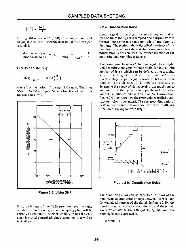
2.2.4 Quantization Noise
Digital signal processing of a signal implies that at specific times the signal is sampled and a digital word is formed that represents the amplitude of the signal at that time. The sections above described the effect of this sampling process, and showed that a minimum loss of information is possible with the proper selection of the input filter and sampling frequency.
The conversion from a continuous signal to a digital signal requires that signal voltage be divided into a finite number of levels which can be defined using a digital word n bits long. An n-bit word can describe 2n different voltage steps. Signal variations between these steps will go undetected. It is therefore necessary to determine the range of signal levels from maximum to minimum that the system must operate with, to determine the number of bits needed in an A/D conversion. Figure 2-9 illustrates how the error voltage (called quantization noise) is generated. The corresponding ratio of peak signal to quantization noise, expressed in dB, is a function of the digital word length.
OUTPUT VOLTAGE
Ja = 2N-1
N = It BITS
Ja ' 6N OB I MAX
I
ERROR I
1
: VOLTAGE" " t\ " 1\ t\ I
'J 'J \I \I \I '\
INPUT VOLTAGE
INPUT VOLTAGE
2 3 4 5 6 7 8 91011 SINO DB "6 18 24 30 36 42 48 54 60 66
Figure 2-9. Quantization Noise
The quantizing error can be expressed in terms of the total mean squared error voltage between the exact and the quantized samples of the signal. In Figure 2-10, any signal voltage v(t) falls between the i-th and the (i+ 1 )th levels which define the i-th quantizing interval. The error signal ei is expressed as
ei=V(t)-Vi

where
SAMPLED DATA SYSTEMS
ei = error voltage between the exact and the ith
quantized voltage levels
V(t) = input signal voltage
Vi = voltage of the ith quantized interval
Figure 2-10. Quantization Step
2-7
Assuming uniform quantization and a uniform distribution of the signal voltage, the resulting signal-toquantization-noise ratio is
S/Nq = M2-1
or, represented as a logarithm,
S/Nq = (6)*(n) dB, n>2
where
S is the peak signal power
Nq is the mean quantization noise
M is the number of quantization levels = 2n
n is the number of bits in the amplitude word
The 2920 has a programmable AID conversion of up to 9 bits of resolution, giving the device up to 54dB of instantaneous dynamic range based on quantization noise alone. For systems where the total dynamic range is >54dB but the instantaneous requirements are within this range, approaches such as automatic gain control, variable attenuators, or programmable amplifiers can be used in conjunction with the 2920. Some of these approaches are discussed in Chapters 4 and 7.

The 2920 Signal Processor 3

CHAPTER 3 THE 2920 SIGNAL PROCESSOR
3.0 THE 2920 SIG NAL PROCESSOR
This chapter will discuss the 2920 device operation functional elements and operating conventions.
3.1 Device Operation
3.1.1 Overview of the 2920
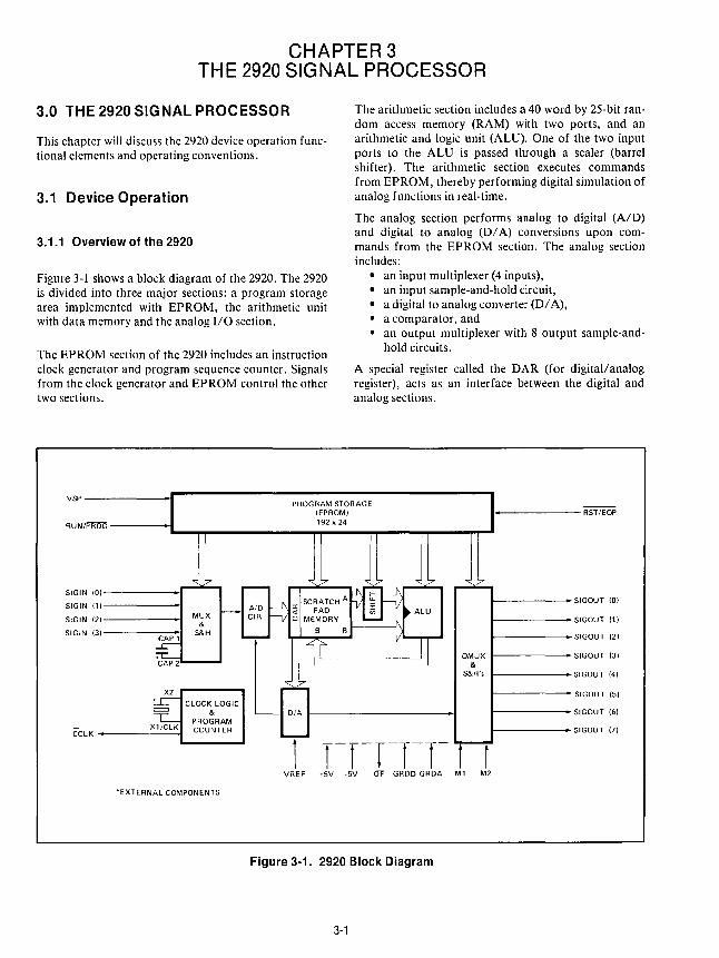
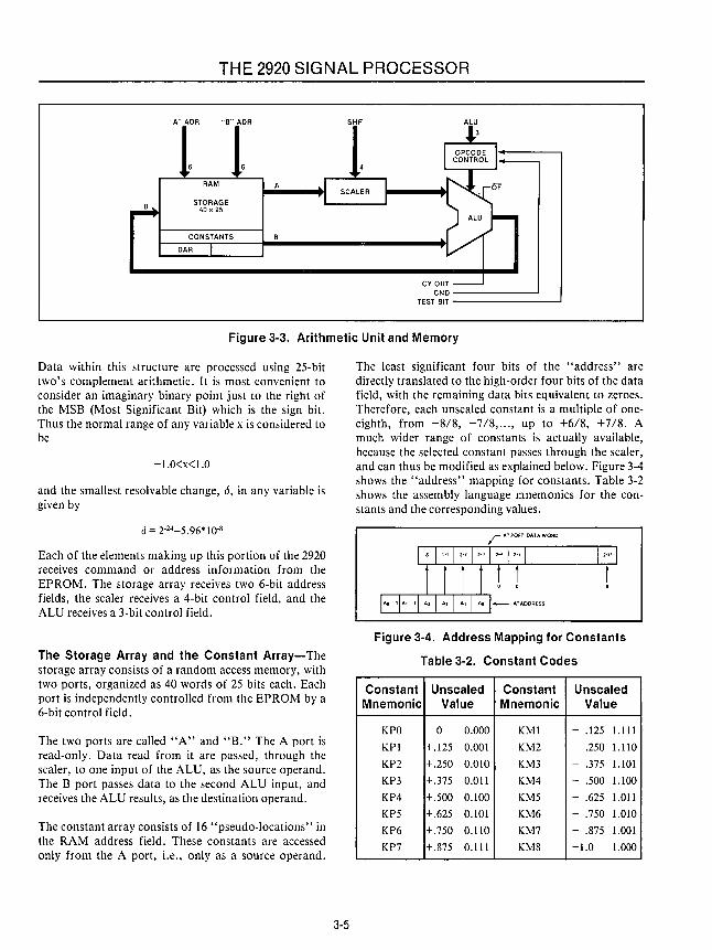
Figure 3-1 shows a block diagram of the 2920. The 2920 is divided into three major sections: a program storage area implemented with EPROM, the arithmetic unit with data memory and the analog 110 section.
The EPROM section of the 2920 includes an instruction clock generator and program sequence counter. Signals from the clock generator and EPROM control the other two sections.
The arithmetic section includes a 40 word by 25-bit random access memory (RAM) with two ports, and an arithmetic and logic unit (ALU). One of the two input ports to the AL U is passed through a scaler (barrel shifter). The arithmetic section executes commands from EPROM, thereby performing digital simulation of analog functions in real-time.
The analog section performs analog to digital (AID) and digital to analog (01 A) conversions upon commands from the EPROM section. The analog section includes:
• an input multiplexer (4 inputs), • an input sample-and-hold circuit, • a digital to analog converter (01 A), • a comparator, and • an output mUltiplexer with 8 output sample-and-
hold circuits.
A special register called the DAR (for digital/analog register), acts as an interface between the digital and analog sections.
VSP------------~--------------------------------------------, PROGRAM STORAGE
(EPROM) 1----------RST/EOP
RUN/PROG--------·L __ ~~--------------~'9:2~X~24~--~----~~----~~
SIGIN (0)----------,
SIGIN (1)-------1
SIGIN (2)-------, SIGIN (3)------1
X2
CCLK _----X-'_/C_LK-I
CLOCK LOGIC &
PROGRAM COUNTER
'EXTERNAL COMPONENTS
1 VREF
Figure 3-1. 2920 Block Diagram
3-1
1------ SIGOUT (0)
1-------- SIGOUT (,)
1------- SIGOUT (2)
DMUX 1-------- SIGOUT (3) &
s&H's 1--------_ SIGOUT (4)
1------ SIGOUT (5)
1-------- SIGOUT (6)
I------SIGOUT (7)
M2
THE 2920 SIGNAL PROCESSOR
3.1.2 Analog Operations
The basic operation of the 2920 can be seen by assuming that an input signal is to be processed, for example by a digital filter, and outputted as an analog signal. Under program control, one input would be selected from the four possible inputs, and the signal sampled and held. This signal would then be converted to a digital word with up to 9 bits of linear conversion (sign bit and 8 amplitude bits).
The bits are formed by a successive approximation AID conversion and stored in the DAR. This DAR register is the interface between the analog and digital sections of the 2920. During AID conversion, the DAR accumulates each bit of the digital word until conversion is complete.
This word may then be loaded into a scratch pad RAM location for further processing. When outputting a value, the 9 most significant bits of a RAM location are loaded into the DAR. Under program control, the DAR drives the 01 A converter, whose output can be routed to any of 8 analog outputs by the output demultiplexer and S&Hs.
3.1.3 Digital Operations
The digital part of the 2920 will be operating simultaneously with the above analog operations. For example, during a 9-bit AID conversion, a 3-pole lowpass filter could be realized using the digital circuitry. The digital loop includes the 2-port addressable 40-word RAM, a binary shifter, and the ALU. Under program control, two 25-bit locations in RAM are simultaneously addressed, with the data from the A address passing through the binary shifter. This shifter allows scaling from 22 (a 2-bit left shift) to 2-13 (a 13-bit right shift). The scaled A value and the unscaled B value are then propagated to the ALU as operands.
The ALU operates on these values with digital instructions specified by the program. The 25-bit result of that operation is loaded into the B address location of the RAM. What makes the 2920 fast enough for real-time processing is that the entire set of actions (analog operation, dual memory fetch, binary shift, ALU execution, and write back to RAM can take place in as little as 400 nanoseconds (depending on the clock rate).
3-2
3.2 A Closer Look at the Functional Elements
3.2.1 EPROM Section
The EPROM section contains 4608 bits of user programmable and erasable read-only memory. In normal operation of the 2920, i.e., in the RUN mode, it is arranged as 192 words of 24 bits each. Each word corresponds to one 2920 instruction. During programming, each 24-bit word is treated as six 4-bit nibbles; i.e., in PROGRAM mode the EPROM appears as 1152 words of four bits each. Figure 3-2 shows the 2920 pin connections for the RUN and PROG mode.
Run Mode-During the RUN mode the EPROM section acts as the system controller. Each 24-bit control word contains bit patterns that determine the operations to be performed by the analog and arithmetic sections.
The control word is composed of five fields, of which one controls the analog section and the remaining four control the arithmetic section. The four arithmetic section control fields include the two 6-bit fields which identifies RAM locations, a 4-bit scaler control field and a 3-bit ALU control field.
In the RUN mode, EPROM word addresses are numbered from 0 to 191. In normal operation alliocations are accessed in sequence and no program jumps are allowed. The EPROM program counter returns to location 0 upon completion of execution of the command in word 191, or when an EOP instruction is encountered in the analog control instruction field. The EOP feature allows the program to be terminated at the end of a user's program shorter than 192 words. Placement of the EOP is explained below.
The EPROM may be thought of as a crystal- or clockcontrolled cycle generator as program length determines the sampling frequency of the analog signals. If an input is sampled once per program pass, the sampling frequency is liNT where N is the number of words (instructions) in the program and T is the time required to execute one instruction.
The EPROM fetchlexecute cycle is pipelined four deep, meaning that the next four instructions are being fetched while the previously fetched instructions are being executed. Although otherwise invisible to the user, this technique requires that the EOP instruction be inserted in a word with an address divisible by four,
THE 2920 SIGNAL PROCESSOR
e.g., program location 0,4, .... ,188. The EOP does not take effect until the three following instructions are executed.
An open drain active low logic pin RST may be used to display the presence of an EOP signal or to apply an external active-low reset signal (which forces a jump to EPROM location zero). This output can sink 2.5mA, which allows connecting a 2.2K pull-up resistor, or one TTL load with a 6.2K pull-up. If the internal EOP instruction is not used, the pin may be tied to VCC or driven by a TTL or CMOS gate. An OR-tied connection may also be used. In normal operation, the 2920 does not use a reset signal, but one may be useful in applications requiring synchronization of the 2920 and other equipment. Proper operation of the EOP instruction requires- an external pull-up resistor on the RST pin.
Since RST and EOP are internally equivalent functions, an externally generated RST must conform to the same rules as the program placement of EOP. CCLK provides this cycle indication and should be used to strobe an externally supplied RST signal.
Two pins associated with the PROGRAM/RUN mode selection are VSP and RUN/PROG. Both pins should be tied to GRDD (digital ground) for RUN mode.
EPROM Program Mode-During programming, each 24-bit EPROM word is treated as six 4-bit nibbles, with the result that the EPROM is programmed as if it were organized as 1152 x 4. Table 3-1 shows the relationship between the control fields and the bit positions in each nibble. (See the sections below on the arithmetic and analog sections for details on the significance of each control bit.)
Many of the pins of the 2920 perform different functions in the PROG mode than they do in the RUN mode. These differences are noted in Figure 3-2.
Note that for the 2920 pin outs as shown in Figure 3-2, the power supply conventions are different for RUN and PROG mode. These conventions allow the programmer designer to use popular TTL family products as a basis for design. With the exception of the power connections, VSP is the only pin that requires other than 5 volt logic levels.
3-3
In the PROG mode, the four pins labelled DO through D3 are used for both data input and output. Their direction is controlled by the PROG/VER pin. A high level on this pin switches to input mode, a low to output. This feature allows the programmed data to be verified before proceeding to the next address. The input data must be presented in true form (logical 1 =high, logical O=low) but is read back complemented (logical 1 =low, 10gicaI0=high).
The internal counters are incremented during the falling edge of INCR. 1152 INCR transitions will complete the full program cycle. To initialize at nibble address 0, RST must be pulsed active (low) and an INCR must be issued.
For programming the RUN/PROG pin must be tied to VBB, the VCC pin to +5 volts, and VSP (the high voltage programming pin) should be pulsed from 5.0 ± .5 volts to +25 ± 1 V @ 15mA max. The data pins DO through D3 have open drains in the output direction; thus pull up resistors are required.
Table 3-1. 2920 Control Bit Assignments/Programming
Nibble Bit Assignment Nibble Number MSB LSB
(3) (2) (1 ) (0)
0 ADFO ADK2 ADKI ADKO 1 A2 Bl Al ADFI 2 A4 B3 A3 B2 3 AO B5 A5 B4 4 S2 Sl SO BO 5 L2 Ll LO S3
3.2.2 Arithmetic Unit and Memory
A block diagram of this subsystem is shown in Figure 3-3, which consists of three major elements: a RAM storage array, a scaler, and an arithmetic and logic unit (ALU).

TH E 2920 SIGNAL PROCESSOR
PIN DESCRIPTIONS (RUN MODE)
Symbol Function
SIGOUT 8 PinS corresponding to the 8 demultl-plexed analog outputs (0-7)
GROA Analog signal ground held at or near GROO tYPically
CAP, & CAP2 External capacitor connections for the Input signal sample and hold CirCUit
VREF Input Reference Voltage
SIGIN 4 pins corresponding to the 4 multi-plexed analog Inputs (0-3)
VBB Most negative power Pin set at -5 volts dUring run mode (different voltage In program mode)
X1/CLK Clock Input when uSing external clock signals, OSCillator Input for external crystal when uSing Internal clock
X2 OSCillator Input for external crystal when uSing Internal clock
GROO Digital ground
Vee 5 volts In run mode
CCLK Internal fetch cycle clock output The failing edge designates the START of a new PROM fetch cycle. CCLK IS 1/16 of X1/CLK rate.
RUN/PROG Mode control tied to GROO In run mode (different voltage In program mode)
RST/EOP Low RST input initializes program fetch counter to first location. As an output It Signifies EOP instruction present (open drain, active low).
PIN DESCRIPTIONS (PROGRAM MODE)
Symbol
00,01,02,03
Function
4 pins carrying EPROM program data for both input and output (open drain, active low output; active high Input)
VB" VB2 VB3 Digital ground In PROGRAM mode (different voltage for RUN mode)
VS" VS2, VS3 +5 volts In PROGRAM mode (function changes for RUN mode)
RUN/PROG Mode control pin tied to VBB for PROGRAM mode (voltage changes for RUN mode)
INCR Input pulse Increments the nibble (4-blts) counter In PROG mode (function changes In RUN mode)
VSP
PROGIVER
EPROM po\',er pin +5 volts for VERIFY mode and +25 volts for PROGRAM mode (different voltage In RUN mode)
Controls EPROM bl-dlrectlonal data bus for venfy (low) or program (high)
Input pulse resets nibble counter to POSition zero for start of programming
Symbol
OF
VSP
M1, M2
Function
Indicates an overflow In the current ALU operation (open drain, active low)
EPROM power Pin 0 volts for RUN mode (Different voltage In program mode)
Two pins which specify the output mode of the SIGOUT pins (see Table 4)
SIGOUT 3 SIGOUT 2
SIGOUT 4 SIGOUT 1
SIGOUT 5 SIGOUT 0
GROA M1
SIGOUT 6 M2
SIGOUT 7 VSP
CAP, OF
VREF RST/EOP
CAP2 RUN/PROG
SIGIN 0 CClK
SIGIN 3 Vee
VBB GROO
SIGIN 2 X2
SIGIN 1 XI/ClK
Run Mode Pin Configuration.
03 02
01
00
VSl
PROG/VER
VSP
INCR
RST
RUN/PROG
Program Mode Pin Configuration.
Figure 3-2. 2920 Pin Descriptions
3-4
THE 2920 SIGNAL PROCESSOR
'A" ADR "B" ADR
RAM
STORAGE 40 x 25
CONSTANTS
DAR
SHF ALU
A
CY OUT CND _____ --J
TEST BIT ---------1
Figure 3-3. Arithmetic Unit and Memory
Data within this structure are processed using 25-bit two's complement arithmetic. It is most convenient to consider an imaginary binary point just to the right of the MSB (Most Significant Bit) which is the sign bit. Thus the normal range of any variable x is considered to be
-1.0<x<1.0
and the smallest resolvable change, d, in any variable is given by
d = 2-24=5.96*10-8
Each of the elements making up this portion of the 2920 receives command or address information from the EPROM. The storage array receives two 6-bit address fields, the scaler receives a 4-bit control field, and the ALU receives a 3-bit control field.
The Storage Array and the Constant Array-The storage array consists of a random access memory, with two ports, organized as 40 words of 25 bits each. Each port is independently controlled from the EPROM by a 6-bit control field.
The two ports are called "A" and "B." The A port is read-only. Data read from it are passed, through the scaler, to one input of the ALU, as the source operand. The B port passes data to the second ALU input, and receives the ALU results, as the destination operand.
The constant array consists of 16 "pseudo-locations" in the RAM address field. These constants are accessed only from the A port, i.e., only as a source operand.
3-5
The least significant four bits of the "address" are directly translated to the high-order four bits of the data field, with the remaining data bits equivalent to zeroes. Therefore, each unsealed constant is a multiple of oneeighth, from -8/8, -718,00', up to +6/8, +7/8. A much wider range of constants is actually available, because the selected constant passes through the scaler, and can thus be modified as explained below. Figure 3-4 shows the "address" mapping for constants. Table 3-2 shows the assembly language mnemonics for the constants and the corresponding values.
~ A" PORT DATA WORD
1 1 II! ! lAS +. -11 A, I A, I A, I Ao 1- A"ADDRESS
Figure 3-4. Address Mapping for Constants
Table 3-2. Constant Codes
Constant Unscaled Constant Unscaled Mnemonic Value Mnemonic Value
KPO 0 0.000 KMI - .125 1.111
KPI +.125 0.001 KM2 - .250 1.110
KP2 +.250 0.010 KM3 - .375 1.101
KP3 +.375 0.011 KM4 - .500 1.100
KP4 +.500 0.100 KM5 - .625 1.011
KP5 +.625 0.101 KM6 - .750 1.010
KP6 +.750 0.110 KM7 - .875 1.001
KP7 +.875 0.111 KM8 -1.0 1.000

THE 2920 SIGNAL PROCESSOR
The DAR can be used as a source or a destination operand. It is both a digital to analog register and an analog to digital register. It is nine bits wide, occupying the nine most significant bit positions of a word whose other bits are set to ones in order to correct for AID conversion number system offset when read into the processor.
The DAR output is also tied directly to the digital to analog converter (DI A) inputs. The DAR is used as a successive-approximation register for analog to digital conversion, under control of the analog function instruction field. Each bit position of the DAR can also be tested by the ALU for conditional arithmetic operations.
Table 3-3. Scaler Codes and Operations
Scaler Bit Equivalent Code Values Multiplier Operation
L02 1110 22= 4.0 "A"x22
LOI 1101 2'= 2.0 "A"x21
ROO 1111 2°= 1.0 "A"x2°
ROI 0000 2-1=0.5 "A"x2-1
R02 0001 2-2= 0.25
R03 0010 2-3= 0.125
R04 0011 2-4= 0.0625 "A"x2-4
R05 0100 2-5= 0.03125
Scaler-The scaler is an arithmetic barrel shifter located between the A port of the RAM and the ALU. Values read from the A port can be shifted left or right. The shifts can be a maximum of two positions to the left or a maximum of thirteen positions right. Left shifts fill with zeroes at the right; right shifts fill with the sign bit at the left.
As explained above, these arithmetic shifts are equivalent to multiplication of the A port value by a power of two, where the number of positions shifted is the 2' s power.
The scaler is controlled by a 4-bit wide control field from the EPROM, as shown in Table 3-3. Note that left shifts may produce numbers which are too large to fit within a 25-bit field. The handling of such large numbers is described in the ALU section below.
The ALU-The Arithmetic Logic Unit calculates a 25-bit result from its A and B operands (source and destination) based on an operation code from the EPROM. The 25-bit result is written back into the B (destination) memory location at the end of the instruction cycle.
One condition for overflow is a left shift where the sense of the sign bit changes. For this reason the ALU uses extended precision to allow calculation of the correct
3-6
Scaler Bit Equivalent Code Values Multiplier
R06 0101 2 6= 0.015625
R07 0110 2 7= 0.0078125
R08 0111 2 8= 0.00390625
R09 1000 2-9= 0.001953125
RIO 1001 2-1°= 0.0009765625
Rll 1010 2- 11 = 0.00048828125
R12 1011 2 12 =0.000244140625
R13 1100 2 -13=0.0001220703125
result even when receiving left-shifted operands from the scaler. If the computed result YY exceeds the bounds
-l.O~YY<l.O
an overflow condition is indicated. When overflow limiting is enabled, this condition causes the result to be replaced with the legal value closest to the desired result, i.e., with -1 if the computed value was negative, and with + 1.0 if the result was positive.
In binary these extreme values appear as
Binary Value
1000 000 000 000 000 000 000 000 -1.0
0111 111 111 111 111 111 111 111 1-2-24
respectively. This overflow saturation characteristic is useful for realizing certain non-linear functions such as limiters, and is beneficial to the stability of filters. The OF pin indicates that an overflow is occurred on the previous operation (cycle). This output is active low and open-drain. In the case where overflow is not enabled, each binary number is extended to 28-bit precision by extending the sign bit to the left. The calculation is done a!1d the low 25 bits are written back to the destination.

THE 2920 SIGNAL PROCESSOR
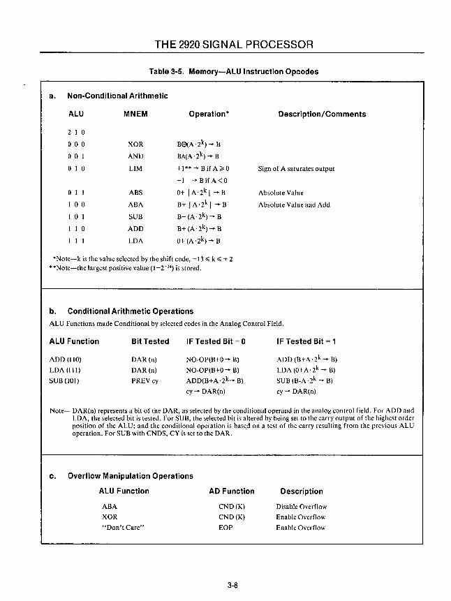
The operations performed by the ALU are summarized in Table 3-5. Although most of them are selfexplanatory, the following details may be useful at this point.
Absolute value (ABS) and absolute add (ABA) convert the" A" operand (source) to its absolute value before performing any calculations. Load A (LOA) and ABS are treated as arithmetic operations by the ALU, meaning that the source is added to zero and then replaces the "B" operand (destination). This causes the correct handling of those overflows caused by left shift operations.
The operation LIM sets the result to positive or negative full scale, based on the "A" port sign bit, behaving much like a forced overflow. However, the overflow flag will not indicate overflow for a LIM unless the given source operand and shiftcode would produce an overflow in an LOA operation.
The constant source codes allow you to select constants for arithmetic operations. The procedure is described in the section on the storage array of the ALU and memory. Table 3-2 above lists the mnemonics and corresponding un scaled value of each constant. Each value is passed through the scaler, and so may be multiplied by a value 2k, where k runs from +2 to -13. The scaler codes and equivalent multiplier values are shown in Table 3-3.
Conditional Arithmetic Operations-In addition to the basic operations described in Table 3-5, some ALU functions may execute conditionally. Certain codes in the analogi digital control field cause the execution of the arithmetic operation to be conditional on a selected bit of the DAR. The conditional instructions are tabulated in Table 3-5b.
The conditional field code selects a bit of the DAR, and uses its value to determine how the instruction is to be executed. A "I" implies execution of the instruction; a "0" implies execution of a NOP. For conditional subtract, the bit actually used is the carry from the previous result. In this case the selected bit of the DAR is set equal to the carry from the current instruction.
Conditional additions are used to mUltiply one variable by a second, as discussed in Chapter 4. The mUltiplier is loaded into the DAR, and the multiplicand is added conditionally to the partial product.
3-7
Conditional subtraction is used to divide one positive variable by another, using a non-restoring division algorithm. The divisor is conditionally subtracted from the dividend, and quotient bits are assembled in the DAR.
Conditional operations may also be useful for performing logic, also shown in Chapter 4. Table 3-4 summarizes the properties of the arithmetic section.
Table 3-4. Memory-ALU Section Summary
ALU result bit width
Number System
Operand A
ALU instruction field width
Scaler instruction field width
"A" and "B" port address field width
Ancillary Instructions
25 bits
2's complement
Read Only Memory Port A, Scaled by shifter, 28 bits wide Read Port B, Unsealed, 25 bits expanded to 28 bit equivalent
3 bits
4 bits
6 bits each
ConditIonal arithmetic, op codes are part of analog control field
Available Storage "A" port, AdrO-39, Read Only, Locations 25 bits. "B" port, AdrO-39,
Read-Write 25 bits.
Digital-Analog-Register "A" port, Adr40, Read Only, 9 MSBs, 16 LSB's are filled with Is. "B" port, same as "A" port but read-write.
Constant Register "A" port only, low 4 bits of adr. Field placed in 4 MSB's of 25-bit width. Low 21 LSB's fill as O's.
Scaler Range 22 (left 2) to TlJ (nght 13).
3.2.3 The Analog Section
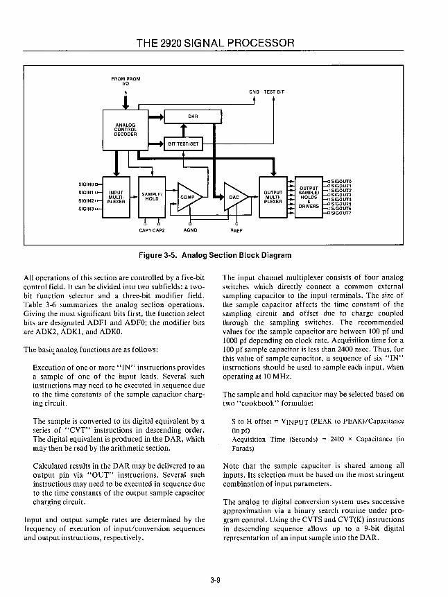
Figure 3-5 shows a detailed block diagram of the 2920's analog section, which provides four analog input channels and eight analog output channels. It includes circuitry for analog-to-digital conversion by successive approximation, and the sample-and-holds for both inputs and outputs.
THE 2920 SIGNAL PROCESSOR
Table 3-5. Memory-ALU Instruction Opcodes
a. Non-Conditional Arithmetic
ALU MNEM Operation*
210
000 XOR BED(A· 2k) .... B
001 AND BA(A·2k) .... B
010 LIM + 1 ** .... B if A ~ 0
-1 .... Bif A<O
o 1 1 ABS 0+ I A·2k I .... B
I 0 0 ABA B+ I A·2k I .... B
I 0 1 SUB B- (A·2k) .... B
I 1 0 ADD B+ (A·2k) .... B
I 1 1 LDA 0+ (A·2k) .... B
*Note-k is the value selected by the shift code, -13 ~ k ~ + 2 * *Note-the largest positive value (1-2-24) is stored.
b. Conditional Arithmetic Operations
Description/Comments
Sign of A saturates output
Absolute Value
Absolute Value and Add
ALU Functions made Conditional by selected codes in the Analog Control Field.
ALU Function Bit Tested IF Tested Bit = 0 IF Tested Bit = 1
ADD (110) DAR (n) NO-OP(B+O .... B) ADD (B+A· 2k .... B)
LDA(lll) DAR (n) NO-OP(B+O .... B) LDA (O+A· 2k .... B)
SUB (101) PREV cy ADD(B+A·2k .... B) SUB (B-A· 2k .... B)
cy .... DAR(n) cy .... DAR(n)
Note- DAR(n) represents a bit of the DAR, as selected by the conditional operand in the analog control field. For ADD and LDA, the selected bit is tested. For SUB, the selected bit is altered by being set to the carry output of the highest order position of the ALU; and the conditional operation is base,d on a test of the carry resulting from the previous ALU operation. For SUB with CNDS, CY is set to the DAR.
c. Overflow Manipulation Operations
ALU Function
ABA
XOR
"Don't Care"
AD Function
CND(K)
CND(K)
EOP
3-8
Description
Disable Overflow
Enable Overflow
Enable Overflow
THE 2920 SIGNAL PROCESSOR
SIGINO
SIGINl
SIGIN2
SIGIN3
FROM PROM 110
CAPl CAP2 AGND
CND TEST BIT
SIGOUTO SIGOUT1 SIGOUT2 SIGOUT3 SIGOUT4 SIGOUT5 SIGOUT6 SIGOUT7
VREF
Figure 3-5. Analog Section Block Diagram
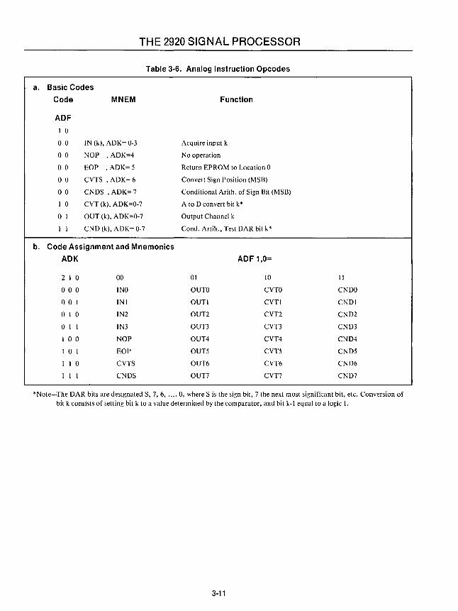
All operations of this section are controlled by a five-bit control field. It can be divided into two subfields: a twobit function selector and a three-bit modifier field. Table 3-6 summarizes the analog section operations. Giving the most significant bits first, the function select bits are designated ADF1 and ADFO; the modifier bits are ADK2, ADK1, and ADKO.
The basis analog functions are as follows:
Execution of one or more "IN" instructions provides a sample of one of the input leads. Several such instructions may need to be executed in sequence due to the time constants of the sample capacitor charging circuit.
The sample is converted to its digital equivalent by a series of "CVT" instructions in descending order. The digital equivalent is produced in the DAR, which may then be read by the arithmetic section.
Calculated results in the DAR may be delivered to an output pin via "OUT" instructions. Several such instructions may need to be executed in sequence due to the time constants of the output sample capacitor charging circuit.
Input and output sample rates are determined by the frequency of execution of input/conversion sequences and output instructions, respectively.
3-9
The input channel multiplexer consists of four analog switches which directly connect a common external sampling capacitor to the input terminals. The size of the sample capacitor affects the time constant of the sampling circuit and offset due to charge coupled through the sampling switches. The recommended values for the sample capacitor are between 100 pf and 1000 pf depending on clock rate. Acquisition time for a 100 pf sample capacitor is less than 2400 nsec. Thus, for this value of sample capacitor, a sequence of six "IN" instructions should be used to sample each input, when operating at 10 MHz.
The sample and hold capacitor may be selected based on two "cookbook" formulae:
S to H offset = VINPUT (PEAK to PEAK)/Capacitance (in pf) Acquisition Time (Seconds) = 2400 x Capacitance (in Farads)
Note that the sample capacitor is shared among all inputs. Its selection must be based on the most stringent combination of input parameters.
The analog to digital conversion system uses successive approximation via a binary search routine under program control. Using the CVTS and CVT(K) instructions in descending sequence allows up to a 9-bit digital representation of an input sample into the DAR.
THE 2920 SIGNAL PROCESSOR
The DAR is a two's complement binary register, nine bits long. When DAR values are delivered to the 01 A, they are converted to sign magnitude format via a one's complement operation. This leads to a potential 1 least significant bit offset during AID conversion, and a half least significant bit offset during 01 A conversion. To compensate for the AID offset, values read from the DAR to the processor have all bits (save the high-order nine) set to ones. 01 A offset may be corrected by subtracting the value 2-9 from the value prior to transferring it to the DAR.
Each CVT cycle sets the selected bit of the DAR to a value derived from the comparator, and also sets the next lower bit to a logic 1. Each cycle must allow the 01 A to settle, so at least two NOP instructions are needed between each pair of successive CVT instructions.
Each of the 2920's eight analog output channels includes an individual sample-and-hold circuit demultiplexed from a common, buffered 01 A output. A separate hold capacitor for each output channel is contained on the 2920.
There are several factors which affect the nature of the output waveform. Writing to the DAR, i.e., using the DAR as the destination, automatically activates signal conditioning circuitry in the buffer amplifier. An "OUT" operation should not appear in an instruction which writes to the DAR. For the most error-free output, the first "OUT" instruction should appear only after the time needed for the amplifier to settle; that is, it should be delayed by several instructions after the one which writes into the DAR. Acquisition time of the output sample-and-hold is typically longer than the instruction cycle, so that a sequence of several "OUT" instructions will usually be necessary.
In many applications, the output signal need only be a logic level of 1 or O. For such functions, the 2920 has provision for using outputs in either analog or logic mode. Two input pins each control four of the outputs. These inputs, designated M 1 and M2, are not TTL compatible, and are not intended to be used to switch modes dynamically while in RUN mode.
When used in logic mode, an output pin appears as an open drain circuit capable of sinking 2.5mA. Thus a CMOS or TTL gate can be driven if a suitable pull-up resistor is used.
A positive voltage reference supply must be provided by the user. The range of acceptable voltages is from + 1 V to +2V and is chosen to suit the application. The input and output voltage range is limited to the range ± VREF. The 01 A is a mUltiplying type and the step size (l LSB) is computed as VREF /256. The current required at VREF, referenced to Analog Ground, falls in the range from 50l1a to 250l1a. Noise appearing on the VREF pin will be transferred directly to the input and output signals through the 01 A. Therefore, VREF must be a noise free voltage source.
3.3 Basic 2920 Performance Parameters and Limits
The limits to 2920 capabilities are established by the size of the on-chip EPROM and RAM, the speed and capability of the processor, and the resolution of the AID and 01 A converters.
A program for the 2920 consists of a series of basic 2920 instructions which are executed sequentially at a fixed rate. The program allows no internal jumps, and is therefore of fixed length and execution time.
A sample interval is the time between samples of the same input channel. Normally, one pass through a program establishes a sample interval, i.e., input/output operations usually take place once per program pass. Similarly, the functions implemented by the sequence of instructions usually occur once per sample interval. However, the signal on a given input channel may be sampled more than once during a single pass through the program. In this case, sample interval is determined by multiplying the instruction-clock-period by the number of instructions between input samples.
The number of functions which can be realized with a single 2920 is established by the amount of EPROM provided and the number of RAM words on the chip. For example, a typical digital filter requires at least one RAM word per pole or two per complex conjugate pole pair. Thus the RAM limits the number of poles to less than 40, or less than 20 complex conjugate pairs. The number of EPROM words needed to realize a complex conjugate pole pair is variable, but has a typical value of approximately 10. Therefore, EPROM capacity also limits the number of conjugate pole pairs to less than 20.
3-10
THE 2920 SIGNAL PROCESSOR
Table 3-6. Analog Instruction Opcodes
a. Basic Codes
Code MNEM Function
ADF
1 0
o 0 IN (k), ADK= 0-3 Acquire input k
o 0 NOP , ADK=4 No operation
o 0 EOP ,ADK=5 Return EPROM to Location 0
o 0 CVTS ,ADK=6 Convert Sign Position (MSB)
o 0 CNDS ,ADK= 7 Conditional Arith. of Sign Bit (MSB)
1 0 CVT (k), ADK=0-7 A to 0 convert bit k*
o 1 OUT (k), ADK=0-7 Output Channel k
1 1 CND (k), ADK= 0-7 Condo Artih., Test DAR bit k*
b. Code Assignment and Mnemonics
ADK ADF 1,0=
210 00 01 10 11
000 INO OUTO CVTO CNDO
001 INI OUTl CVTl CNDI
010 IN2 OUT2 CVT2 CND2
o 1 1 IN3 OUT3 CVT3 CND3
100 NOP OUT4 CVT4 CND4
1 0 1 EOP OUT5 CVT5 CND5
1 0 CVTS OUT6 CVT6 CND6
1 I CNDS OUT7 CVT7 CND7
*Note-The DAR bits are designated S, 7, 6, .... 0, where S is the sign bit, 7 the next most significant bit, etc. Conversion of bit k consists of setting bit k to a value determined by the comparator, and bit k-l equal to a logic 1.
3-11

Building Block Functions- 4 Foundation of Design

CHAPTER4 BUILDING BLOCK FUNCTIONS-FOUNDATION OF DESIGN
"4.0 BUILDING BLOCK FUNCTIONSFOUNDATION OF DESIGN
The Intel 2920 Signal Processor is typically thought of in terms of the functions it can implement, rather than in terms of its architecture, as is more common with microprocessors. A long list of building block fuactions can be defined and 2920 assembly language code written for each one, possibly using the interactive Signal Processing Applications Software/Compiler. The system is then implemented by combining the building blocks as required. This is directly analogous with the normal design procedure of specifying a detailed block diagram of the desired system and then designing each block to specifications individually before combining them into the total system.
Building block functions can be lumped into general functions such as filtering, waveform generation, or non-linear functions. Table 4-1 indicates the number of instructions and RAM locations needed for some typical functions.
This table may be used to do a rough estimate of program length needed for a given application by assigning the required number of instructions to each block of the system block diagram. Once the program complexity has been estimated, the range of sample rates can be determined along with the corresponding signal bandwidth. Ideally, the signal bandwidth could be half the sample rate. When practical considerations such as antialiasing and reconstruction filter complexity are taken into account, signal bandwidths on the order of one third or one fourth the sampling rate are typical.
Table 4-2 gives the sample rate and corresponding maximum signal bandwidth as a function or program size. To better appreciate the complexity of a system that can be implemented with a given size program, three examples are given in Table 4-3 which are representative of a wide variety of possible applications.
4.1 Arithmetic Building Blocks
Among the simplest and most essential routines to be used in building more complex functions are multiplication and division, both by constants and by variables. This section describes such routines.
4.1.1 Elementary Arithmetic
The basic arithmetic instructions of the 2920 allow addition of one variable to another, subtraction of one
4-1
variable from another, or replacement of one variable by another in a single instruction, for example in assembly language:
ADD X, Y;
adds the value associated with the RAM location labelled X to the value in the RAM location labelled Y. No scaler code was specified; the default condition is equivalent to ROO.
Similarly, the value to be added or subtracted can be scaled by a power of two in a single instruction: e.g.,
SUB Y, X, R02;
causes one fourth of the value associated with X to be subtracted from the variable Y. The equivalent FORTRAN language statements for the operations above would be:
Y=Y+X Y = Y - (.25 * X)
respectively.
In general, the instruction set of the 2920 makes it quite easy to implement the equivalent of the FORTRAN statement:
y=y+(c * X)
where C is an arbitrary constant.
The last statement includes the equivalent of multiplication of X by an arbitrary constant. The next section describes some general rules for performing this basic operation.
4.1.2 Multiplication by a Constant
The number of 2920 steps required to perform an operation of the type
y=y+(c * X)
is determined by the value and accuracy of the constant C.
Any value C can be expressed as sums and differences of positive and negative powers of two. Once a constant C is expressed in this way, the equivalent to Y = Y + (C * X) can be easily converted to 2920 code.
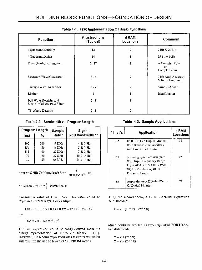
BUILDING BLOCK FUNCTIONS-FOUNDATION OF DESIGN
Table 4-1. 2920 Implementation Of Basic Functions
Function # Instructions
(Typical)
4 Quadrant Multiply 12
4 Quadrant Divide 14
Filter Quadratic Function 7 -12
Sawtooth Wave Generator 3-7
Triangle Wave Generator 5-9
Limiter 1
Full Wave Rectifier and 2-4 Single Pole Low Pass Filter
Threshold Detector 2-4
Table 4-2. Bandwidth vs. Program Length
Program Length Sample Signal Inst % Rate* 3 dB Bandwidth* *
!
192 100 13KHz 4.33 KHz 154 80 16KHz 5.33 KHz 115 60 22KHz 7.33 KHz
77 40 32KHz 10.7 KHz 39 20 65 KHz 21.7 KHz
* Assumes 10 MHz Clock Rate. Sample Rate = 19 Hz (# inst)(400x 10- )
I ** Assume BW3 dB::: 3 (Sample Rate)
Consider a value of C = 1.875. This value could be expressed several ways. For example:
1.875 = 1.0 + 0.5 + 0.25 + 0.125 = 20 + 2-1 +2-2 + 2-3
or:
1.875 = 2.0 - .125 = 21 - 2-3
The first expression could be easily derived from the binary representation of 1.875 (in binary: 1.111). However, the second expression uses fewer terms, which will result in the use of fewer 2920 EPROM words.
4-2
#RAM Comment Locations
2 9 Bit X 25 Bit
3 25 Bit ~ 9 Bit
2 A Complex Pole or
Complex Zero
2 9 Bit Amp Accuracy > 16 Bit Freq. Ace
2 Same as Above
1 Ideal Limiter
1
2
Table 4-3. Sample Applications
# Inst's Application #RAM Locations
192 1200 BPS Full Duplex Modem 38
With Xmit & Receive Filters And Line Equalization
155 Scanning Spectrum Analyzer 23
With Input Frequency Range From 200 Hz to 3.2 KHz With
100 Hz Resolution, 48dB Dynamic Range
115 Approximately 22 Poles/Zeros 24
Of Digital Filtering
Using the second form, a FORTRAN-like expression for Y becomes
y = y + (21 * X) - (2-3 * X)
which could be written as two sequential FORTRANlike statements:
y= Y+(21 >I< X)
Y = Y - (2-3 * X)
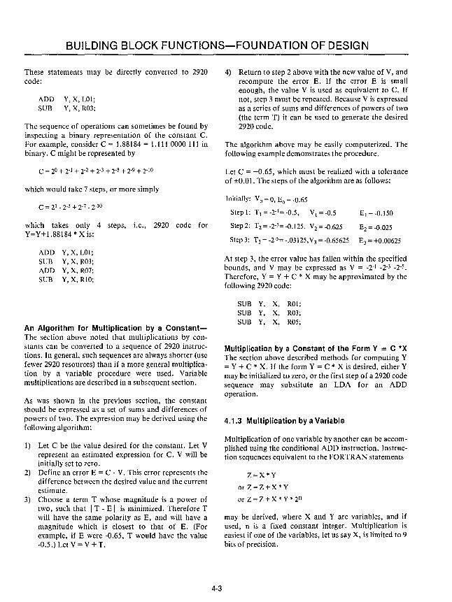
BUILDING BLOCK FUNCTIONS-FOUNDATION OF DESIGN
These statements may be directly converted to 2920 code:
ADD Y, X, LOl; SUB Y, X, R03;
The sequence of operations can sometimes be found by inspecting a binary representation of the constant C. For example, consider C = 1.88184 = 1.111 0000 111 in binary. C might be represented by
which would take 7 steps, or more simply
which takes only 4 steps, i.e., 2920 code for Y=Y+1.88184 * X is:
ADD Y,X, LOl; SUB Y, X, R03; ADD Y, X, R07; SUB Y, X, RIO;
An Algorithm for Multiplication by a ConstantThe section above noted that multiplications by constants can be converted to a sequence of 2920 instructions. In general, such sequences are always shorter (use fewer 2920 resources) than if a more general multiplication by a variable procedure were used. Variable multiplications are described in a subsequent section.
As was shown in the previous section, the constant should be expressed as a set of sums and differences of powers of two. The expression may be derived using the following algorithm:
1) Let C be the value desired for the constant. Let V represent an estimated expression for C. V will be initially set to zero.
2) Define an error E = C - V. This error represents the difference between the desired value and the current estimate.
3) Choose a term T whose magnitude is a power of two, such that IT - E I is minimized. Therefore T will have the same polarity as E, and will have a magnitude which is closest to that of E. (For example, if E were -0.65, T would have the value -0.5.) Let V = V + T.
4-3
4) Return to step 2 above with the new value of V, and recompute the error E. If the error E is small enough, the value V is used as equivalent to C. If not, step 3 must be repeated. Because V is expressed as a series of sums and differences of powers of two (the term T) it can be used to generate the desired 2920 code.
The algorithm above may be easily computerized. The following example demonstrates the procedure.
Let C = -0.65, which must be realized with a tolerance of ±0.01. The steps of the algorithm are as follows:
Initially: V 0 = 0, Eo = -0.65
Step 1: T1 =-2-b -0.5, VI=-0.5 EI = -0.150
Step 2: T2 =-2-3=-0.125, V2 =-0.625 E2=-0.025
Step 3: T3 = -2-5= -.03125,V3 = -0.65625 E3 = +0.00625
At step 3, the error value has fallen within the specified bounds, and V may be expressed as V = -2-1 -2-3 _2-5•
Therefore, Y = Y + C * X may be approximated by the following 2920 code:
SUB Y, X, ROl; SUB Y, X, R03; SUB Y, X, R05;
Multiplication by a Constant of the Form Y = C *X The section above described methods for computing Y = Y + C * X. If the form Y = C * X is desired, either Y may be initialized to zero, or the first step of a 2920 code sequence may substitute an LDA for an ADD operation.
4.1.3 Multiplication by a Variable
Multiplication of one variable by another can be accomplished using the conditional ADD instruction. Instruction sequences equivalent to the FORTRAN statements
z=X*y
or Z = Z +X * Y
or Z = Z + X * Y * 2n
may be derived, where X and Yare variables, and if used, n is a fixed constant integer. Multiplication is easiest if one of the variables, let us say X, is limited to 9 bits of precision.
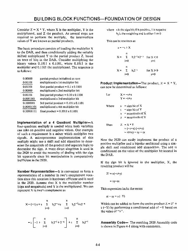
BUILDING BLOCK FUNCTIONS-FOUNDATION OF DESIGN
Consider Z = X * Y, where X is the multiplier, Y is the multiplicand, and Z the product. As several steps are required to perform the multiply, the intermediate values of Yare known as partial products.
The basic procedure consists of loading the multiplier X to the DAR, and then conditionally adding the suitably shifted multiplicand Y to the partial product Z, based on tests of bits in the DAR. Consider multiplying the binary values '0.1011 x 0.1101, where 0.1011 is the multiplier and 0.1101 the multiplicand. The sequence is as follows:
0.00000 0.01101
0.01101 0.00000
0.01101 0.0001101
0.1000001 0.00001101
0.10001111
partial product initialized to zero multiplicand x 1st multiplier bit
first partial product = 0.1 x 0.1101 multiplicand x 2nd multiplier bit
2nd partial product = 0.10 x 0.1101 multiplicand x 3rd multiplier bit
3rd partial product = 0.101 x 0.1101 multiplicand x 4th multiplier bit
final product = 0.1011 x 0.1101
Implementation of a 4 Quadrant Multiplier-A four-quadrant multiply is needed when both variables can take on positive and negative values. One example of such a requirement is a mixer which multiplies two signals. A microprocessor implementation of this mUltiply might use a shift and add algorithm to determine the magnitude of the product and separate logic to determine the sign. A more direct alogrithm is used in the 2920 to avoid the necessity of dealing with the sign bit separately since bit manipulation is comparatively inefficient in the 2920.
Number Representation-It is convenient to form a representation of a number in two's complement notation since this notation is hardware efficient and is used in the 2920. Assume that X is the multiplier number (sign and magnitude) and Y is the multiplicand. We can represent X in two's complement as
n n x = (-1) s + s }: b.2-·+s }: b.2- i+sTn
i=O i=O
4-4
where s is the sign bit; 0 is positive, 1 is negative bi is the weighting and is either 1 or 0
This can be rewritten as
x= -s+X
n X = }: b.2-i+2-n for X < 0
i=O s=1
n X = }: b.2-· for X ;;?; 0
i=O s=O
Product Implementation-The product, Z = X * Y, can now be determined as follows:
Let
Where
X = -s+x Y = -t+y
s = sign bit of X t = sign bit of Y x = magnitude o(X y = magnitude of Y
Then Z =X * Y = (-s+x) (-t+y) = st+xy - sy - tx
Now the 2920 can easily implement the product of a positive multiplier and a bipolar multicand using a simple shift and conditional add alogorithm. The add is conditioned on the value of the multiplier bit located in the DAR.
If the sign bit is ignored in the multiplier, X, the resulting product will be
Z' = x(-t+y)
= xy-tx
This expression lacks the terms
st - sy = s (-Y)
Which can be added to form the entire product Z = Z' + s (-Y) by performing a conditional add of -Y based on the value of "s".
Assembly Code- The resulting 2920 Assembly code is shown in Figure 4-1 along with comments.

BUILDING BLOCK FUNCTIONS-FOUNDATION OF DESIGN
OP Dest Source SHF CND Comments
LDA DAR X ROO --- SET UP DAR FOR CONDITIONAL ADD'S, X IS MULTIPLIER
ADD Z Y ROI CND7
ADD Z Y R02 CND6
ADD Z Y R03 CND5 MUL T1PLY Y BY THE MAGNITUDE OF X, THAT IS x WHERE
ADD Z Y R04 CND4
ADD Z Y R05 CND3 Z = x (-t+y)
ADD Z Y R06 CND2
ADD Z Y R07 CNDI
ADD Z Y R08 CNDO
SUB Y Y LOI --- DEVELOPE-Y
Y-2Y=-Y
ADD Z Y ROO CNDS CONDITIONAL ADD OF "-Y" IF SIGN OF X IS NEGATIVE
SUB Y Y LOI --- RESTORES ORIGINAL SIGN OF Y IF NEEDED
Figure 4·1. 4 Quadrant Multiply In 2920 Code
4.1.4 Division by a Variable CY=O 1.11011 +.000111
CY=O 1.111101 +.0000111
CY=1 0.0000001 -.00000111
CY=O 1.11111011
The quotient so far = 0.10010
Division of a variable by a constant may be performed by mUltiplying the variable by a value equal to the inverse of the constant. However, to divide a variable by another variable uses the conditional subtract. The basic alogrithm is intended for division of positive numbers by positive numbers. If negative variables are to be used, the sign of the quotient may be computed using XOR and the absolute magnitudes of the variables are used.
The full sequence for a four quadrant divide (Y=X/W)
The sequence consists of conditionally subtracting the divisor from the dividend, with the quotient being assembled in the DAR. The sequence is started with an unconditional subtraction which should be scaled to produce a negative result.
Consider dividing 0.100 by 0.111
0.1000000 -0.111
CY=O 1.1010000 +.0111
CY=1 0.00010000 -.00111
initial subtract
first carry, partial remainder 1st conditional subtract (does add)
4-5
becomes as follows:
LOA TMP, XOR TMP, ABS X, ABS W, SUB X, SUB X, SUB X, SUB X, SUB X, SUB X,
SUB X, SUB X, SUB X, XOR DAR,
W, R13 X, R13 X, ROO W, ROO W, ROO W, ROl, CND7 W, R02, CND6 W, R03, CND5 W, R04, CND4 W, R05, CND3 W, R06, CND2 W, R07, CNOl W, R08, CNDO
TMP, R13
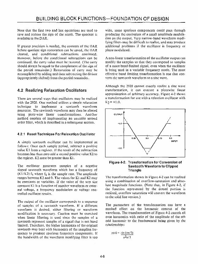
BUILDING BLOCK FUNCTIONS-FOUNDATION OF DESIGN
Note that the first two and last operations are used to save and restore the sign of the result. The quotient is available in the DAR.
If greater precision is needed, the contents of the DAR before quotient sign restoration can be saved, the DAR cleared, and conditional subtractions continued. However, before the conditional subtractions can be continued, the carry value must be restored. (The carry should always be equal to the complement of the sign of the partial remainder.) Restoration of carry may be accomplished by adding and then subtracting the divisor (appropriately shifted) from the partial remainder.
4.2 Realizing Relaxation Oscillators
There are several ways that oscillators may be realized with the 2920. One method utilizes a simple relaxation technique to implement a sawtooth waveform generator. The sawtooth waveform may then be altered using piece-wise linear transformations. Another method consists of implementing an unstable second order filter, which is described in a subsequent section.
4.2.1 Reset Technique For Relaxation Oscillator
A simple sawtooth oscillator can be implemented as follows: Once each sample period, subtract a positive value Kl from a register. If the result of the subtraction becomes less than zero add a second positive value K2 to the register. K2 must be greater than K I.
The oscillator generates samples of a negative sloped sawtooth waveform which has a frequency of (KlIK2) fs where fs is the sample rate. The amplitude ranges between K2 and O. The values for Kl and K2 may be constants or variables. If the value of the step size constant KI is a function of another waveform or external voltage, a frequency modulation or voltage controlled oscillator resul ts.
The output of the oscillator corresponds to a sequence of samples of a sawtooth waveform. If a different waveform is desired, either filtering or waveform modification is necessary. Caution must be exercised when linear filtering is used since the samples of a sawtooth represent samples of a signal that is not band limited. Therefore, the higher harmonics of the original sawtooth may beat with harmonics of the sampling frequency to produce spurious frequency components. If the bandwidth of the waveform modifying filter is too
4-6
wide, some spurious components could pass through producing the equivalent of a small amplitude modulation on the output. Very narrow-band waveform modifying filters may be difficult to realize, and may produce additional problems if the oscillator is frequency or phase modulated.
A non-linear transformation of the oscillator output can modify the samples so that they correspond to samples of a more band-limited signal, even when the oscillator is being used in a variable frequency mode. The most effective band limiting transformation is one that converts the sawtooth waveform to a sine wave.
Although the 2920 cannot exactly realize a sine wave transformation, it can execute a piecewise linear approximation of arbitrary accuracy. Figure 4-2 shows a transformation for use with a relaxtion oscillator with K2 = +1.0.
OUTPUT
+1.0
-1.0
\ \
/ \ I V
/ /
I
INPUT
Figure 4-2. Transformation for Conversion of Sawtooth Waveform to Clipped Triangle
The transformation shown in Figure 4-2 can be realized using a combination of overflow-saturation and absolute magnitude functions. (Note that, in Figure 4-2, if the function represented by the dotted portion is realized, overflow saturation will convert the waveform to the solid line version.)
The parameters of the transformation can have a marked effect on the harmonic content of the waveform. The transformation of Figure 4-2 cancels all even harmonics with ratio of the amplitude of the nth odd harmonic to the fundamental being given by the relationships:
p(n) = sin (nrr/3)
n2rr/3

BUILDING BLOCK FUNCTIONS-FOUNDATION OF DESIGN
Therefore, the third harmonic is absent, the fifth is down 28db, the seventh is down 34db, etc. This represents a much lower harmonic content than the original sawtooth which contains all harmonics in a ratio p(n) = .i.
n
The 2920 code for this transformation is given below. The oscillator, represented by the variable name OSC, is assumed to be a sawtooth between + 1.0 and O. The comments indicate the steps the waveform transformation takes. Note the use of a constant KP4 to readjust DC levels.
LDA Y asc ROO ; Sawtooth + 1.0 to 0
SUB y KP4 ROO ; Sawtooth + O.S to -0.5
ABS y y LOI ; Triangle 0 to 1.0
SUB y KP4 ROO ; Triangle -O.S to O.S
ADD y y LOI ; Clipped Triangle
Example-A program for an oscillator which generates the clipped triangle wave approximation to a sine wave for a frequency of 1070Hz = 0.1 0/0. Assume a sample interval of 76.8/isec.
The value for K1 may be found by solving the oscillator frequency equation above.
KI =.!....* K2 fs
In binary, for 1070Hz ± 1.07 Hz and K2 = 1.0,
.0001010100000100 ~ KI ~ .0001010100001110
A value of K1 = .0001010100001 = 2-~+2-6+2-8+2-13 corresponds to 1069.7Hz. The program for the oscillator then becomes as follows:
SUB asc, KPS, R03
SUB asc, KP4, R07
SUB asc, KP4, RI2
LDA DAR, asc, ROO
ADD asc, KP4, LOI, CNDS ; conditional ADD K2
Note the use of the 2920 constants to generate the desired values for K1, and K2, and the use of the conditional ADD to perform the K2 addition, which resets the osciIlator. This code may be followed by that realizing the waveform modification of Figure 4.2 to complete the generation of the clipped triangle output.
4-7
4.2.2 Overflow Technique for Relaxation Oscillator
It is possible to generate a sawtooth waveform using the overflow disable operations described in Table 3-4c. In some cases this technique may yield a shorter overall program length. The technique involves using the "wraparound" characteristics of a non-overflow corrected 2's complement number system; that is, if you add 1 to the most positive number, the result will be the most negative number. In its simplest form, a sawtooth or "ramp" may be developed using the following 2920 code:
ABA asc KP4 R07 CND(K)
where the ABA with CND(K) instruction disables overflow correction and the non-CND(K) part increments the value OSC by a constant (2-8 in this-example).
4.3 Voltage Controlled Oscillators (VCQ's)
The basic relaxation oscillator described above may be frequency modulated or voltage controlled by replacing K1 with a suitably weighted variable from the controlling voltage or modulating signal.
If the variable V represents the instantaneous value of the modulating signal and a frequency relationship of the form F = fo + A V is desired, then the algorithm for the oscilfator becomes as follows:
1) At each sample period, subtract the value (fo +AV) K2/fs from the oscillator register.
2) If the register contents become negative, add K2 to the oscillator.
The value (fo+AV)K2Ifs can be separated into constant and variable terms.
constant term = fo K2!fs
variable term = AV * K2!fs
Because 2920 realizations of VCO's are sampled, the usual considerations for alias distortion must be made. The output of the VCO will represent a sampled version of the corresponding continuous signal. Because frequency modulation can produce fairly wide side bands (in addition to those due to waveform), this side band energy is a potential source of alias distortion if it has
BUILDING BLOCK FUNCTIONS-FOUNDATION OF DESIGN
significant components above half the sample rate. For this reason, the maximum frequency excursion of the VCO should be kept well below half the sample rate.
4.4 Oscillators Based On Unstable Second-Order Sections
A second order filter with poles on the imaginary axis of the s-plane (unit circle of the z-plane) is predicted to act as an oscillator with a stable sine-wave output. A stage of this type may be used as the basis of a sine-wave oscillator. However, the amplitude of the oscillation is determined by the initial values in the filter, and the slightest deviation of the pole locations can cause the amplitude to grow or decay.
One approach to this type of oscillator is to place the poles so that the oscillation grows slowly with time, with overflow saturation limiting the growth. Many simple LC oscillators operate in this mode. The technique is also applicable to the 2920, but the user must be aware of the differences between continuous (analog) and discrete (digital) oscillators. The continuous oscillator starts because small amounts of noise provide an initial excitation of the unstable pole pair. For example, if the second order section initially has Y 1 = Y2 = 0, the stage will provide zero output rather than oscillations, unless it is excited by some external input.
To prevent such a degenerate solution, it may be necessary to measure the oscillator amplitude, and "strike" the oscillator to start it. The amplitude measure may be obtained by low-pass filtering the rectified output, with striking being accomplished by making X = 0 if and only if the amplitude exceeds some minimum value.
The equations for an oscillator are similar to those of a second order filter. If the oscillator frequency and growth should be of the form
A . eat sin (bt)
where b = 2nfo and fo is the desired oscillator frequency, then the coefficients should be (for sample in terval T):
BJ = 2e -aT cos bt
B2= -e-2 aT
Note that the magnitude of B2 is now slightly greater than one. The size of "a" determines the rate at which oscillations grow in amplitude. Larger values cause
4-8
faster starting, but at the expense of frequency accuracy. In addition, overflow saturation may produce undesirable effects on oscillator behavior. Each time saturation is entered the oscillator behaves as if a small quantity was added to YO. Such a change corresponds to a change in both amplitude and phase. The amplitude change may introduce undesired harmonic content and the phase change may result in a change of frequency, so that the oscillator runs at a somewhat different rate than initially predicted.
A second, somewhat related effect is that of locking to sample rate. Because any finite digital system has a finite number of states, eventually an oscillator must repeat states. Once a state has repeated, the entire sequence of output samples then repeats indefinitely. When a particular state is periodically forced by the occurrences of overflow saturation, the length of the repetition period may be shortened considerably, with the effect that the oscillator frequency fosc, takes the form: fosc=(KlIK2)fs. In the equation, K2 represents the number of samples in one repetition, and Kl represents the number of cycles of the oscillator in that period. The sample rate is designated fs. The harder the oscillator "hits the stops", i.e., the larger the value of "a", the shorter the repeat cycle will be. Actual evaluation of repeat cycle length, etc., is probably best achieved by computer simulation.
4.5 Gain Controlled Oscillator
The oscillator described above is equivalent to a continuous positive feedback oscillator, in which oscillations grow until the loop gain is reduced by amplifier saturation. Another type of continuous oscillator uses gain control to determine oscillator amplitude. An early realization of a gain controlled continuous oscillator used an incandescent lamp in the positive feedback loop. A rising amplitude heated the lamp filament, raising its resistance and reducing the oscillator's positive feedback.
An equivalent oscillator realized with the 2920 will consist of an amplitude measurement, with the value of "a" (in the equations for Bl and B2) being a function of the amplitude. A positive "a" causes the oscillation amplitude to rise, while a negative value produces a falling amplitude.
Normally both Bl and B2 must be varied, but it is possible to limit the variation to B2 if a small frequency variation is tolerable. In this mode Bl is fixed at a value
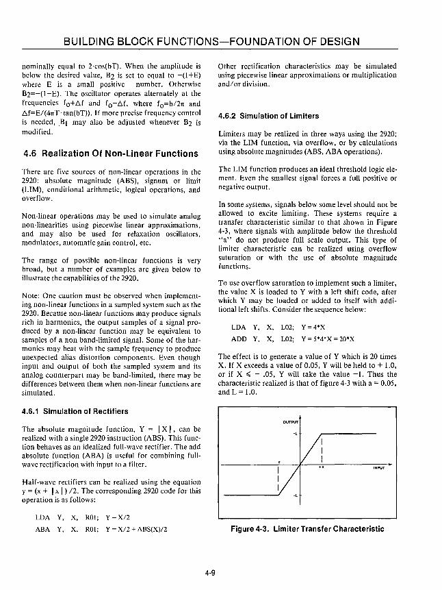
BUILDING BLOCK FUNCTIONS-FOUNDATION OF DESIGN
nominally equal to 2·cos(bT). When the amplitude is below the desired value, B2 is set to equal to -(1 +E) where E is a small positive number. Otherwise B2=-(l-E). The oscillator operates alternately at the frequencies fo+b.f and fo-b.f, where fo=bl2rr and b.f=E/(4rrT· tan(bT». If more precise frequency control is needed, .Bl may also be adjusted whenever B2 is modified.
4.6 Realization Of Non-Linear Functions
There are five sources of non-linear operations in the 2920: absolute magnitude (ABS), signum or limit (LIM), conditional arithmetic, logical operations, and overflow.
Non-linear operations may be used to simulate analog non-linearities using piecewise linear approximations, and may also be used for relaxation oscillators, modulators, automatic gain control, etc.
The range of possible non-linear functions is very broad, but a number of examples are given below to illustrate the capabilities of the 2920.
Note: One caution must be observed when implementing non-linear functions in a sampled system such as the 2920. Because non-linear functions may produce signals rich in harmonics, the output samples of a signal produced by a non-linear function may be equivalent to samples of a non band-limited signal. Some of the harmonics may beat with the sample frequency to produce unexpected alias distortion components. Even though input and output of both the sampled system and its analog counterpart may be band-limited, there may be differences between them when non-linear functions are simulated.
4.6.1 Simulation of Rectifiers
The absolute magnitude function, Y = I X I, can be realized with a single 2920 instruction (ABS). This function behaves as an idealized full-wave rectifier. The add absolute function (ABA) is useful for combining fullwave rectification with input to a filter.
Half-wave rectifiers can be realized using the equation y = (x + I x I ) 12. The corresponding 2920 code for this operation is as follows:
LDA Y, X, ROl; Y = X/2
ABA Y, X, ROl; Y = XI2 + ABS(X)12
4-9
Other rectification characteristics may be simulated using piecewise linear approximations or multiplication and/or division.
4.6.2 Simulation of Limiters
Limiters may be realized in three ways using the 2920; via the LIM function, via overflow, or by calculations using absolute magnitudes (ABS, ABA operations).
The LIM function produces an ideal threshold logic element. Even the smallest signal forces a full positive or negative output.
In some systems, signals below some level should not be allowed to excite limiting. These systems require a transfer characteristic similar to that shown in Figure 4-3, where signals with amplitude below the threshold "a" do not produce full scale output. This type of limiter characteristic can be realized using overflow saturation or with the use of absolute magnitude functions.
To use overflow saturation to implement such a limiter, the value X is loaded to Y with a left shift code, after which Y may be loaded or added to itself with additionalleft shifts. Consider the sequence below:
LDA Y, X, L02; Y = 4*X
ADD Y, X, L02; Y = 5*4*X = 20*X
The effect is to generate a value of Y which is 20 times X. If X exceeds a value of 0.05, Y will be held to + 1.0, or if X ~ - .05, Y will take the value -1. Thus the characteristic realized is that of figure 4-3 with a = 0.05, and L = 1.0.
OUTPUT
1/ _____ --J -L
INPUT
Figure 4·3. Limiter Transfer Characteristic
BUILDING BLOCK FUNCTIONS-FOUNDATION OF DESIGN
Another realization can be based on the equation LOA T, X, ROO;
SUB T, A, ROO; X-A in T y = I x-a I - I x+a I
ABS Y, T, ROO; Y=ABS(X-A)
which realizes the same shape curve as that of Figure ADD T, A, LOI; X+A in T
4-3, with a value of L = 2a. This form generally takes ABS T, T, ROO; ABS (X+A) in T more steps than the overflow saturation method, but
SUB Y, T, ROO; Y = ABS( X-A) - ABS( X+A) allows greater freedom in setting parameters. The 2920 code might appear as follows, where A represents the limiter threshold, and T is a location used only for intermediate calculations:
4-10
Summary of 5 Filter Characteristics


CHAPTER 5 SUMMARY OF FILTER CHARACTERISTICS
5.0 SUMMARY OF FILTER CHARACTERISTICS
This section presents a general review of different filter types and discusses their characteristic weak and strong points. It then presents a comparative analysis which aids in the selection of a filter for implementation and testing.
5.1 Characteristics Of "Ideal" Filters
It is useful to examine the characteristics of transmission lines and the so-called "ideal" filter as an introduction to typical filter characteristics.
Distortionless transmission implies that a signal is transmitted through a network or medium and is received exactly as sent but delayed by some amount. A Fourier Analysis of the required transfer function shows that it must have a constant amplitude over all frequencies and a linear phase shift with frequency. An example of a distortionless system is a length of transmission line with a phase slope proportional to its length. Any amplitude shaping as a function of frequency will introduce some measure of distortion to the signal. The problem then is to achieve the required frequency selectivity while minimizing the distortion of the signal.
5.1.1 The Rectangular Filter
An ideal filter can be defined as follows for purposes of analysis: it has a linear phase characteristic and a bandlimited amplitude response, i.e., unity in the passband and zero in the stopband. This filter provides the asymptotic limit in filter selectivity with a minimum of distortion. Realizable filters can approach this selectivity by increasing the number of poles or stopband zeros in their transmission function. Phase linearity must be maintained either by employing direct linear phase synthesis techniques or by using phase equalizers to linearize the phase characteristic of the fil ter.
It is of interest to study the pulse transient response of the rectangular filter as a limiting case of high selectivity filter development. The pulse response can be calculated as a function of pulse width and filter bandwidth using Fourier Analysis techniques. The following equation is derived for the output response:
5-1
h(t) = KnV
{ Si [(B)(t-to +~~ -Si [(B)(t-to-i)]}
where h(t) is the output pulse response
x Si(x) = J
o sin y
dy y
K is the filter passband gain V is the input pulse amplitude T is the pulse width B is the filter bandwidth
Figure 5-1 illustrates the pulse response as a function of the TB product.
Do ~ <I:
(a) Lowpass-Fllter Pulse Response
(b) Response 01 Rectangular Lowpass FIlter to a Unit Input Pulse
TIME
Figure 5-1. Rectangular Filter Pulse Response
As the pulse-duration bandwidth product approaches infinity, the output pulse shape approaches that of the input pulse in rise time and amplitude. One important difference is that overshoot and ringing on the output pulse does not diminish in amplitude as the bandwidth of the filter is increased toward infinity. Instead, overshoot approaches 9070 of the steady-state pulse height, and settling time approaches zero as bandwidth approaches infinity. This characteristic is referred to as
SUMMARY OF FILTER CHARACTERISTICS
the Gibbs phenomenon, and is explained mathematically by the fact that the Fourier Series expansion of a function fails to converge uniformly at discontinuities. This point is significant because it shows that the transient response of a filter is closely related to the selectivity of the filter, and that phase linearization will not eliminate overshoot and ringing.
5.2 Minimum Phase Filters
A minimum phase filter is defined as a filter whose transfer function has all poles in the left plane and no zeros in the right half plane of the complex frequency s-plane. When a function is minimum phase, its phase response is uniquely related to its amplitude response, i.e., an amplitude specification uniquely defines the phase characteristic of the filter. This attribute makes it possible to categorize filter design parameters for a limited selection of amplitude and phase characteristics. These filters are the ones most often taken from design tables ("cookbook filter design") and include Butterworth, Chebyshev, Bessel, Transitional Bessell Butterworth, Equal Ripple Phase, Elliptic Function, and other less well-known designs. Each of these filters provides unique characteristics which makes it a valuable contribution to filter design. The "best" filter from this group depends on the application: in some cases a number of them may be satisfactory, while in others none will suffice. The following sections describe the basic characteristics of these filters from an applications viewpoint.
5.2.1 Butterworth Filters
Butterworth filters are also called "maximally flat amplitude" filters because they are specifically designed to have monotonically flat amplitude response, with a nearly zero slope over the majority of the passband. Outside the passband these filters exhibit good selectivity, with the amplitude rolloff approaching 6dB/octavebandwidth per pole and an ultimate rejection approaching infinity as the frequency moves away from the passband.
The pulse response of these filters is characterized by high overshoot and significant ringing. The overshoot increases monotonically with the number of poles, and the duration of the ringing is inversely proportional to the filter bandwidth (as it is in all minimum phase filters.) The poor pulse response is caused by both the high selectivity and the nonlinear phase characteristics of the filters.
5-2
Typical applications of this type of filter include signal rejection, frequency domain shaping of a spectrum, or other amplitude response applications where the phase distortion of the signal is not important (e.g., filtering a fixed tuned linear oscillator.)
5.2.2 Chebyshev Filters
These filters are also called "equal ripple amplitude" filters because the passband gain is defined within specific limits, between which the gain varies in a sinusoidal manner. The number of amplitUde ripples is related to the number of poles in the transfer function. The amount of ripple is determined by specifying the transfer function with typical values of 0.01 to 0.5 dB. The attenuation outside the passband increases monotonically towards infinity. For an equal number of poles, the Chebyshev filter has a higher rate of rolloff in the vicinity of the passband cutoff frequency than the Butterworth filter. This rolloff eventually approaches a 6 dB/octave-bandwidth per pole rate.
The pulse response exhibits only slightly greater overshoot than the Butterworth, but condsiderably more ringing. The amount of ringing is proportional to the amplitUde ripple magnitude. The phase response also has a ripple component roughly proportional to the amplitUde ripple. One would properly suspect that this filter introduces more distortion into a signal which occupies the entire filter bandwidth. It can be shown that over restricted portions of the passband, the combined phase linearity and amplitude distortion effects may be less for Chebyshev than for Butterworth and Bessel filters.
The Chebyshev filter is usually used in applications where a high selectivity, high ultimate rejection, and low complexity are desired.
5.2.3 Elliptic Function Filters
The highest selectivity minimum phase filters are elliptic function filters, characterized by equal ripple amplitude in the passband and the stopband. The design parameters are the amount of ripple in the passband, the minimum attentuation in the stopband, and the transition region width from passband to stopband. These filters use zeros in the stopband to achieve exceptional selectivity, but have a finite ultimate attenuation equal to the minimum attenuation. In some applications this finite rejection can be a problem for interference which is not sufficiently attenuated in the stop band.
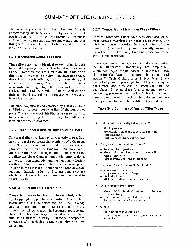
SUMMARY OF FILTER CHARACTERISTICS
The pulse response of the elliptic function filter is approximately the same as for Chebyshev filters, and possibly even better for the same selectivity. The phase and time delay characteristics are sufficiently bad that this type of filter is seldom used where signal distortion is a strong consideration.
5.2.4 Bessel and Gaussian Filters
These filters are nearly identical to each other in both time and frequency domains. The Bessel is also known as the Thompson and the maximally flat time delay filter. Unlike the high selectivity filters described above, these filters are primarily designed for linear phase and good transient response. Their selectivity is roughly comparable to a single stage RC section within the first 6 dB regardless of the number of poles. Well outside their passband the rolloff approaches 6 dB/octavebandwidth per pole.
The pulse response is characterized by a fast rise time and little or no overshoot regardless of the number of poles. One application of this filter is as a matched filter to receive pulse signals in a noisy but otherwise interference-free environment.
5.2.5 Transitional Gaussian/Butterworth Filters
This useful filter provides the skirt selectivity of a Butterworth but the passband characteristics of a Gaussian filter. The transitional point is established by varying a parameter in the transfer function, transition points values of 6 dB or 12 dB being common. This means that the filter exhibits a Gaussian amplitude response down to the transition amplitude, and then assumes a Butterworth amplitude response. The filter has good phase linearity in the passband, though not as good as a conventional Gaussian filter, and a transient response which has substantially reduced overshoot compared to a Butterworth.
5.2.6 Other Minimum Phase Filters
Many other transfer functions can be described, such as equal ripple phase, parabolic, monotonic L, etc. Their characteristics are combinations of those already described. The important aspect of minimum phase filters is the unique relationship between amplitude and phase. The transient response is affected by both parameters, so that flexibility is limited with respect to simultaneously achieving good selectivity and low distortion.
5-3
5.2.7 Comparison of Minimum Phase Filters
Lowpass prototype filters have been discussed which meet various magnitude or phase requirements. For minimum phase networks, the specification of one parameter (magnitude or phase) necessarily constrains the other. Thus, both amplitude and phase cannot be specified independently.
Filters synthesized for specific amplitUde properties include Butterworth (maximally flat amplitude), Chebyshev (equal ripple passband amplitude), and elliptic function (equal ripple amplitude passband and stopband). Optimal phase filters include Bessel (maximally flat phase), equal ripple time delay (equal ripple phase error), and transitional (compromised amplitUde and phase). Some of these filter types and the corresponding properties are iisted in Table 5-1. A comparison can be made in both the time domain and frequency domain to illustrate the different properties.
Table 5-1. Summary of Analog Filter Types
• Butterworth "maximally flat amplitude"
- Flat in passband - Monotonic in stopband to zero gain at 00 Hz - High selectivity - High overshoot transient response
• Chebyshev "equal ripple amplitude"
. - Small ripples in passband - Monotonic in stopband to zero gain at 00 Hz - Higher selectivity - Higher overshoot transient response
• Elliptic or cauer "equal ripple amplitude"
- Ripples in passband - Ripples in stopband to Amin - Highest selectivity - Highest overshoot transien t response
• Bessel "maximally flat delay"
- Monotonic amplitude in passband and stopband - Poor selectivity - Nearly linear phase and flat time delay - Zero overshoot transient response
• Allpass
- Flat amplitude (constant gain) - Used to equalize phase or delay characteristics of
networks
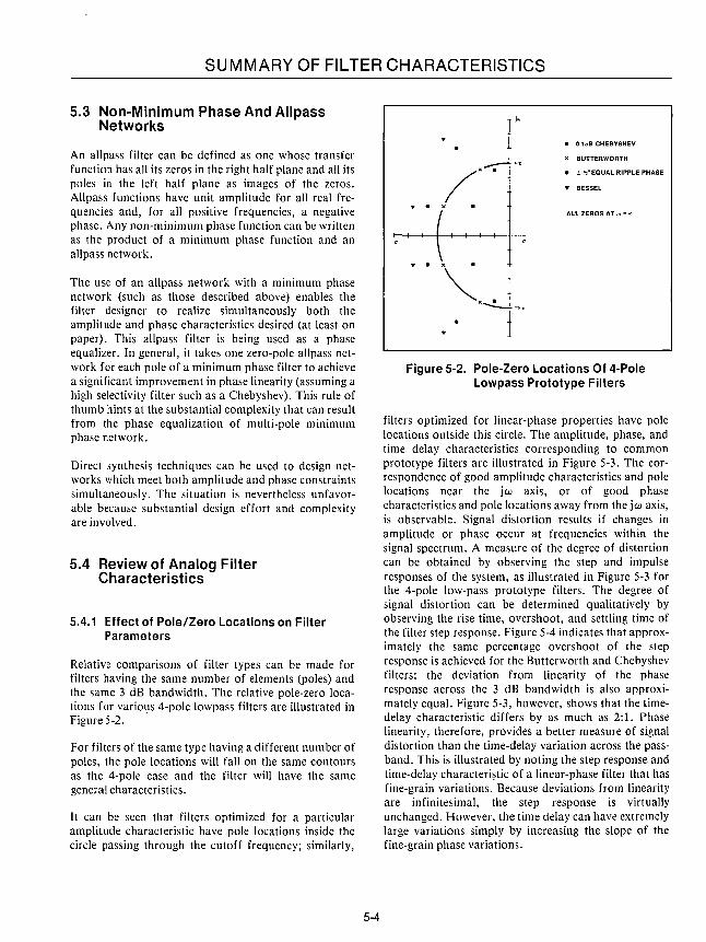
SUMMARY OF FILTER CHARACTERISTICS
5.3 Non-Minimum Phase And Allpass Networks
An allpass filter can be defined as one whose transfer function has all its zeros in the right half plane and all its poles in the left half plane as images of the zeros. Allpass functions have unit amplitude for all real frequencies and, for all positive frequencies, a negative phase. Any non-minimum phase function can be written as the product of a minimum phase function and an allpass network.
The use of an allpass network with a minimum phase network (such as those described above) enables the filter designer to realize simultaneously both the amplitude and phase characteristics desired (at least on paper). This allpass filter is being used as a phase equalizer. In general, it takes one zero-pole allpass network for each pole of a minimum phase filter to achieve a significant improvement in phase linearity (assuming a high selectivity filter such as a Chebyshev). This rule of thumb hints at the substantial complexity that can result from the phase equalization of multi-pole minimum phase network.
Direct synthesis techniques can be used to design networks which meet both amplitude and phase constraints simultaneously. The situation is nevertheless unfavorable because substantial design effort and complexity are involved.
5.4 Review of Analog Filter Characteristics
5.4.1 Effect of Pole/Zero Locations on Filter Parameters
Relative comparisons of filter types can be made for filters having the same number of elements (poles) and the same 3 dB bandwidth. The relative pole-zero locations for variol;ls 4-pole lowpass filters are illustrated in Figure 5-2.
For filters of the same type having a different number of poles, the pole locations will fall on the same contours as the 4-pole case and the filter will have the same general characteristics.
It can be seen that filters optimized for a particular amplitude characteristic have pole locations inside the circle passing through the cutoff frequency; similarly,
5-4
)w
• 0 laB CHEBYSHEV
)( BUTTERWORTH
• ± 'h'EQUAL RIPPLE PHASE
T BESSEL
ALL ZEROS AT w = ~
I \
'f' • \ . ~"~
Figure 5-2. Pole-Zero Locations Of 4-Pole Lowpass Prototype Filters
filters optimized for linear-phase properties have pole locations outside this circle. The amplitude, phase, and time delay characteristics corresponding to common prototype filters are illustrated in Figure 5-3. The correspondence of good amplitude characteristics and pole locations near the jw axis, or of good phase characteristics and pole locations away from the jw axis, is observable. Signal distortion results if changes in amplitude or phase occur at frequencies within the signal spectrum. A measure of the degree of distortion can be obtained by observing the step and impulse responses of the system, as illustrated in Figure 5-3 for the 4-pole low-pass prototype filters. The degree of signal distortion can be determined qualitatively by observing the rise time, overshoot, and settling time of the filter step response. Figure 5-4 indicates that approximately the same percentage overshoot of the step response is achieved for the Butterworth and Chebyshev filters; the deviation from linearity of the phase response across the 3 dB bandwidth is also approximately equal. Figure 5-3, however, shows that the timedelay characteristic differs by as much as 2: 1. Phase linearity, therefore, provides a better measure of signal distortion than the time-delay variation across the passband. This is illustrated by noting the step response and time-delay characteri~tic of a linear-phase filter that has fine-grain variations. Because deviations from linearity are infinitesimal, the step response is virtually unchanged. However, the time delay can have extremely large variations simply by increasing the slope of the fine-grain phase variations.

SUMMARY OF FILTER CHARACTERISTICS
4 S
NORMALIZED FREOUENCY
I ISO
~ '" i 100
SO
NORMALIZED FREQUENCY
NORMALIZED FREQUENCY
Figure 5-3. Amplitude, Phase, And Time-Delay Characteristics Of Lowpass Prototype Filters
5.4.2 Transient Response and Selectivity
Because the use of all pass networks allows the synthesis of a phase characteristic independent of the amplitude response, it is of interest to know how phase linearization of standard minimum phase filters affects their transient response. A study of the step response of such synchronously tuned filter stages as the passive RC networks indicates that the rise time of the filter decreases (Le., responds faster), when its phase characteristic is linearized. The step response of a single-pole network is illustrated in Figure 5-5. Because the rise time of cascaded filter sections is approximately equal to the
5-5
04
03
BESSEL /"1, ./ BUTTERWORTH
!,' .t. ~ 01 dB CHEBYSHEV
!' :\, ·M· ... / ±OS'LINEARPHASE
!/ ! :~ ". !' i ~\ .,
! / ! / "I ". "/' .1,'
02 if / \\ \ '\ i/ :/ \\ \
01''1/ \, \,
· /J '\,.i~;;y--",;~--.~ -01~------~------~~---------L--------~
o
10
08
04
12 TIME
Lr-~.~-.-.-.==~--_~ ,..." I .... ----:.=..::--' --/:, I, ~
/.~/ ""'01 dB CHEBYSHEV II i~ ~BUTTERWORTH
.' • , BfSSEL
,; :j/ /' ~ ±O S' LINEAR PHASE
,., /' / 1
l;,)" i;/ ;.,/
o «j;Y
Figure 5-4. Impulse And Step Response Of Lowpass Prototype Filters
18
square root of the sum of the squares of the individual stage rise times, the results for a single stage can be extended to mUltiple stages.
An interesting result of the analysis of such filter characteristics as selectivity and overshoot appears when percent overshoot (in response to a step input) is plotted as a function of filter selectivity. Two separate curves arise which are related to the phase characteristics of the filters. Linear or nearly linear phase
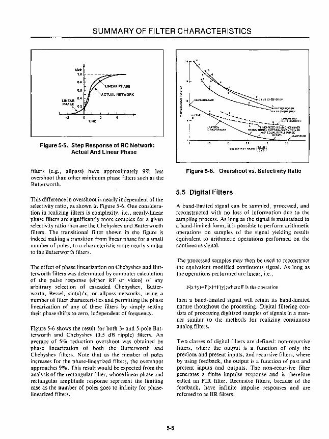
SUMMARY OF FILTER CHARACTERISTICS
-2
AMP 1.0 - - - - - - - -
LINEAR PHASE
~ACTUALNETWORK
1/RC
Figure 5·5. Step Response of RC Network: Actual And Linear Phase
filters (e.g., allpass) have approximately 9010 less overshoot than other minimum phase filters such as the Butterworth.
This difference in overshoot is nearly independent of the selectivity ratio, as shown in Figure 5-6. One consideration in realizing filters is complexity, i.e., nearly-linear phase filters are significantly more complex for a given selectivity ratio than are the Chebyshev and Butterworth filters. The transitional filter shown in the figure is indeed making a transition from linear phase for a small number of poles, to a characteristic more nearly similar to the Butterworth filters.
The effect of phase linearization on Chebyshev and Butterworth filters was determined by computer calculation of the pulse response (either RF or video) of any arbitrary selection of cascaded Chebyshev, Butterworth, Bessel, sin(x)/x, or allpass networks, using a number of filter characteristics and permitting the phase linearization of any of these filters by simply setting their phase shifts to zero, independent of frequency.
Figure 5-6 shows the result for both 3- and 5-pole Butterworth and Chebyshev (0.5 dB ripple) filters. An average of 5% reduction overshoot was obtained by phase linearization of both the Butterworth and Chebyshev filters. Note that as the number of poles increases for the phase-linearized filters, the overshoot approaches 9%. This result would be expected from the analysis of the rectangular filter, whose linear phase and rectangular amplitude response represent the limiting case as the number of poles goes to infinity for phaselinearized filters.
5-6
20
15
3 BUTTERWORTH
05 dB CHEBYSHEV : ............................. ; ......... .............. ............. LINEARIZED
/ ....... -. __ -:;::: ____ ~~BUTTERWORTH
w4ATTEN 3 "LINEARIZED 0 5-;; CHEBYSHEV LINEAR PHAse TRANSITIONAL BUTT/GAUSSIAN TO 6 dB
,- 05° EQUAL RIPPLE PHASE ,- B;SSEL ,-GAUSSIAN
O,L----~----~------~----~~---a-----
SELECTIVITY RATIO (3:::)
Figure 5·6. Overshoot vs. Selectivity Ratio
5.5 Digital Filters
A band-limited signal can be sampled, processed, and reconstructed with no loss of information due to the sampling process. As long as the signal is maintained in a band-limited form, it is possible to perform arithmetic operations on samples of the signal yielding results equivalent to arithmetic operations performed on the continuous signal.
The processed samples may then be used to reconstruct the equivalent modified continuous signal. As long as the operations performed are linear, i.e.,
F(x+y)=F(x)+F(y);where F is the operation
then a band-limited signal will retain its band-limited nature thoughout the processing. Digital filtering consists of processing digitized samples of signals in a manner similar to the methods for realizing continuous analog filters.
Two classes of digital filters are defined: non-recursive filters, where the output is a function of only the previous and present inputs, and recursive filters, where by using feedback, the output is a function of past and present inputs and outputs. The non-recursive filter generates a finite impulse response and is therefore called an FIR filter. Recursive filters, because of the feedback, have infinite impulse responses and are referred to as IIR filters.
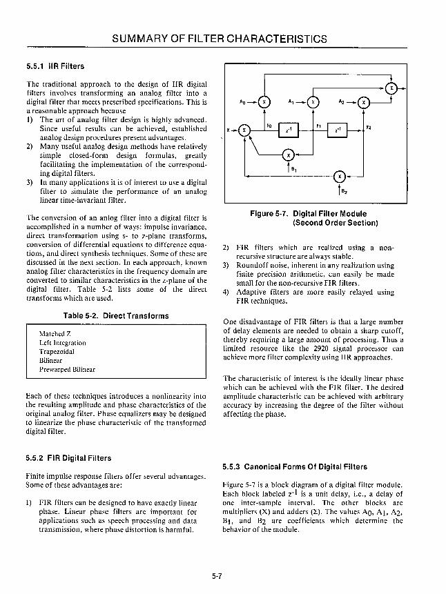
SUMMARY OF FILTER CHARACTERISTICS
5.5.1 II R Filters
The traditional approach to the design of IIR digital filters involves transforming an analog filter into a digital filter that meets prescribed specifications. This is a reasonable approach because 1) The art of analog filter design is highly advanced.
Since useful results can be achieved, established analog design procedures present advantages.
2) Many useful analog design methods have relatively simple closed-form design formulas, greatly facilitating the implementation of the corresponding digital filters.
3) In many applications it is of interest to use a digital filter to simulate the performance of an analog linear time-invariant filter.
The conversion of an anlog filter into a digital filter is accomplished in a number of ways: impulse invariance, direct transformation using s- to z-plane transforms, conversion of differential equations to difference equations, and direct synthesis techniques. Some of these are discussed in the next section. In each approach, known analog filter characteristics in the frequency domain are converted to similar characteristics in the z-plane of the digital filter. Table 5-2 lists some of the direct transforms which are used.
Table 5-2. Direct Transforms
Matched Z Left Integration Trapezoidal Bilinear Prewarped Bilinear
Each of these techniques introduces a nonlinearity into the resulting amplitude and phase characteristics of the original analog filter. Phase equalizers may be designed to linearize the phase characteristic of the transformed digital filter.
5.5.2 FIR Digital Filters
Finite impulse response filters offer several advantages. Some of these advantages are:
1) FIR filters can be designed to have exactly linear phase. Linear phase filters are important for applications such as speech processing and data transmission, where phase distortion is harmful.
5-7
·--------.,0 t 62
Figure 5-7. Digital Filter Module (Second Order Section)
2) FIR filters which are realized using a nonrecursive structure are always stable.
3) Roundoff noise, inherent in any realization using finite precision arithmetic, can easily be made small for the non-recursive FIR filters.
4) Adaptive filters are more easily relayed using FIR techniques.
One disadvantage of FIR filters is that a large number of delay elements are needed to obtain a sharp cutoff, thereby requiring a large amount of processing. Thus a limited resource like the 2920 signal processor can achieve more filter complexity using IIR approaches.
The characteristic of interest is the ideally linear phase which can be achieved with the FIR filter. The desired amplitude characteristic can be achieved with arbitrary accuracy by increasing the degree of the filter without affecting the phase.
5.5.3 Canonical Forms Of Digital Filters
Figure 5-7 is a block diagram of a digital filter module. Each block labeled z-I is a unit delay, i.e., a delay of one inter-sample interval. The other blocks are multipliers (X) and adders (L). The values AO, AI, A2, B 1, and B2 are coefficients which determine the behavior of the module.
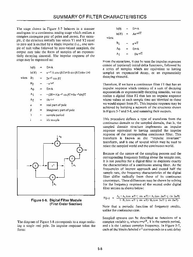
SUMMARY OF FILTER CHARACTERISTICS
The stage shown in Figure 5-7 behaves in a manner analogous to a continuous analog stage which realizes a complex conjugate pair of poles and zeroes. For example, if the structure initially has values Y 1 and Y2 equal to zero and is excited by a single impulse (i.e., one sample of unit value followed by zero-valued samples), the output may take the form of samples of an exponentially decaying sinusoid. The impulse response of the stage may be expressed as:
when
h(O) D+A
h(iT) e-a•T A cos ({3iT)+B sin ({3iT) for i>O
BI 2e-aT cos {3T
B2 -e-2aT
AO D+A
Al -(2D+A)e-aT cos{3T+Be-aTsin{3T
A2 De-2aT
a real part of pole
{3 imaginary part of pole
T sample period
ith sample
Figure 5-8. Digital Filter Module (First Order Section)
The diagram of Figure 5-8 corresponds to a stage realizing a single real pole. Its impulse response takes the form:
5-8
h(O) D+A
h(iT) Ae-aiT
when
BI e-aT
AO D+A
Al -De-aT
From the equations, it can be seen the impulse responses consist of (optional) initial delta functions, followed by a series of samples which are equivalent to having sampled an exponential decay, or an exponentially decaying sinusoid.
Therefore, if we have a continuous filter FI that has an impulse response which consists of a sum of decaying exponentials or exponentially decaying sinuoids, we can realize a digital filter F2 that has an impulse response whose values at each sample time are identical to those we would expect from Fl. This impulse response may be achieved by building a network of the structures shown in Figure 5-7 and 5-8, and summing their outputs.
This procedure defines a type of transform from the continuous domain to the sampled domain, that is, the sampled domain structure implements an impulse response equivalent to having sampled the impulse response of the corresponding continuous filter. This transform is known as the "impulse invariant" transform, and is one of several which may be used to relate the sampled world and the continuous world.
Because of the nature of the sampling process and the corresponding frequency folding about the sample rate, it is not possible for a digital filter to duplicate exactly the characteristics of a continuous analog filter. As the frequencies of interest approach and exceed half the sample rate, the frequency characteristics of the digital filter differ radically from those of its continuous counterpart. These differences may be shown by solving for the frequency response of the second order digital filter section as shown below:
F(jw) = Ao + AI (cos wT-j sin wT) + A2 (cos 2wT-j sin 2wT)
I-B I (cos wT-j sin wT)-B2 (cos 2wT-j sin 2wT)
Note that a periodic function of frequency results, unlike the continuous case.
Sampled systems can be described as functions of a complex variable z, where z=esT , T is the sample period, and s is the Laplace complex frequency. In Figure 5-7, each of the blocks labeled z-I corresponds to a unit delay

SUMMARY OF FILTER CHARACTERISTICS
of time T. It is possible to describe the characteristics of the block diagram of Figure 5-7 as a ratio of polynomials in z or z-l.
Consider the case of a continuous analog filter where one stage realizes a single exponentially decaying sinusoid. Just as such a structure corresponds to a single pair of complex conjugate poles, the diagram shown in Figure 5-8 is capable of realizing a single exponentially decaying sinusoid and corresponds to a single complex conjugate pair of poles in the complex z plane. Figure 5-9 shows a plot of the frequency response of the typical second order continuous section, and, for comparison, that of a second order sampled section, for the case where the impulse invariant transform described above was used.
5.5.4 Matched Z Transform
Another method for converting from the s-plane to the z-plane is known as the matched z transform. This method is simply a technique for mapping each pole or zero of the s-plane to a corresponding pole or zero in the z-plane. A pole or zero at a+jb on the s plane is transferred to a pole or zero at e(a+jb)T on the z-plane, where T represents the sample interval in seconds. In polar coordinates, this z-plane location is (eaT,bT) The equations for the filter coefficients are shown below:
Second order sections for a continuous pole pair -a±jb in the s-plane.
B) = 2e-at cos bT
B2= -e-2aT
for a continuous zero pair at -a±jb
A) = 2Aoe-aT cos bT
A2 = Aoe-2aT
First order section
for a real pole at -a
B) = e-aT
for a real zero at -a
A) = -Aoe-aT
This transform is not guaranteed equivalence in either frequency or time domains, although pole positions correspond to the impulse invariant transform. The transform is sometimes useful for conceptually estimating the influence, on the resulting filter characteristic, of moving the poles or zeros. In general, it is easier to predict the impact on frequency response of moving a pole or zero in the s-plane than in the z-plane, because the s-plane axes are more directly related to frequency.
The matched z transform allows a one-to-one correspondence of poles and zeros in the s-plane to poles and zeros in the z-plane. One use of this transform is therefore to aid manipulation of the positions of poles and zeros in the z-plane in order to achieve some desired frequency response.
Rather than attempt to do the complete design on the s-plane and then transform to the z-plane to achieve the desired filter, the designer manipulates the poles and
frequency
Figure 5-9. Comparison of Digital and Continuous Frequency Response
5-9
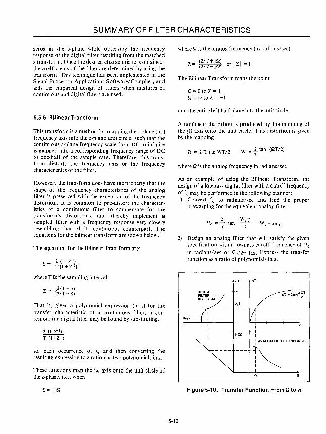
SUMMARY OF FILTER CHARACTERISTICS
zeros in the s-plane while observing the frequency response of the digital filter resulting from the matched z transform. Once the desired characteristic is obtained, the coefficients of the filter are determined by using the transform. This technique has been implemented in the Signal Processor Applications Software/Compiler, and aids the empirical design of filters when mixtures of continuous and digital filters are used.
5.5.5 Bilinear Transform
This transform is a method for mapping the s-plane (jw) frequency axis into the z-plane unit circle, such that the continuous s-plane frequency scale from DC to infinity is mapped into a corresponding frequency range of DC to one-half of the sample rate. Therefore, this transform distorts the frequency axis or the frequency characteristics of the filter.
However, the transform does have the property that the shape of the frequency characteristics of the analog filter is preserved with the exception of the frequency distortion. It is common to pre-distort the characteristics of a continuous filter to compensate for the transform's distortions, and thereby implement a sampled filter with a frequency response very closely resembling that of its continuous counterpart. The equations for the bilinear transform are shown below.
The equations for the Bilinear Transform are:
where T is the sampling interval
z .... (2IT + S) (2/T - S)
That is, given a polynomial expression (in s) for the transfer characteristic of a continuous filter, a corresponding digital filter may be found by substituting.
2 (l_Z-I)
T (l+Z-I)
for each occurrence of s, and then converting the resulting expression to a ration to two polynomials in z.
These functions map the jw axis onto the unit circle of the z-plane, i.e., when
S= jQ
where Q is the analog frequency (in radians/sec)
_ (2IT+jQ) _ Z - (2IT _ jQ) or I Z I - 1
The Bilinear Transform maps the point
Q=OtoZ = 1 Q = 00 to Z =-1
and the entire left half plane into the unit circle.
A nonlinear distortion is produced by the mapping of the jQ axis onto the unit circle. This distortion is given by the mapping
Q = 2IT tan WT12 W = 1- tan-I (QT12)
T
where Q is the analog frequency in radians/sec
As an example of using the Bilinear Transform, the design of a lowpass digital filter with a cutoff frequency of fc may be performed in the following manner: 1) Convert fc to radians/sec and find the proper
prewarping for the equivalent analog filter:
2 WeT Q c =-::r tan -2- We= 2rrfc
2) Design an analog filter that will satisfy the given specification with a lowpass cutoff frequency of Q c in radians/sec or Q c12rr Hz. Express the transfer function as a ratio of polynomials in s.
5-10
H(w)
DIGITAL FILTER RESPONSE
wT
HIQ)
wT
I I I
Q
I ANALOG FILTER RESPONSE I
Q
Figure 5-10. Transfer Function From Q to w
SUMMARY OF FILTER CHARACTERISTICS
3) Use the bilinear transform on the transfer function in s (obtained in step 2) to obtain a transfer function in z, i.e., replace each occurance of s with
2 (1 -z-l)
T (1 + z-l)
The digital filter which corresponds to the z-plane expression from step 3 (Figure 5-10) will now have the desired cutoff characteristic.
Note that this transform may alter the number of poles and zeros involved. If poles and zeros are independently transformed, redundant poles or zeros may occur. Using this transform requires careful elimination of such redundancies.
5.6 Implementing Filters with the 2920
Once you have determined the locations of your filter's poles and zeros in the z-plane, converting this structure into 2920 code is relatively straightforward. In the blocks of Figures 5-7 and 5-8, there are three basic operations performed to achieve digital filtering action: a unit delay, addition, and multiplication.
For time invariant filters, the multiplications performed for digital filters will be of some variable Yi by a constant represented by the values Ao, AI, A2, BI, or B2. The goal of the 2920 programmer is to implement these functions with a minimum of 2920 instructions.
Unit Delay-The blocks labeled z-I correspond to unit delays, i.e., delays of one sample interval. The sample interval is the time it takes for the 2920 to make one pass through its program. The value on the output side of a delay block represents the value computed'at the block's input on the previous pass through the program.
The delay can be realized by a RAM location which retains the data from the previous pass until it is needed. A single LDA instruction of the 2920 is sufficient to implement a unit delay block. Figure 1 shows two delay blocks; thus two LDA instructions and two RAM locations are required. These instruction have the form shown below:
LDA Y2, YI, ROO LDA YI, YO, ROO
5-11
After executing these two instructions, the RAM location designated Y2 contains the value of Y 1 from the previous pass, and Y 1 contains the value of YO from the previous pass. To complete the filter realization, it is sufficient to complete the calculations of the new value of YO from the current values of input, Y 1, and Y2, and then compute the output from YO, Yl, and Y2. The new value of YO involves multiplication of Yl and Y2 by the constants Bl and B2. The instruction set of the 2920 permits implementing these multiplications-byconstants as a series of addition and subtraction steps.
Implementing Coefficients-In general, the coefficients are not realized exactly, but rather are approximated as closely as necessary to meet the filter specifications. This permits minimizing the number of 2920 program steps required to realize the multiplications.
Each ADD or SUB instruction of the 2920 can be thought of as adding a value to (or subtracting it from) the destination operand (e.g., Yl in the last instruction above). The value used in that operation is the product of some power of two and the source operand (e.g., YO in the last instruction above). There is a simple algorithm for converting a multiplication by a constant into a series of additions and subtractions. It consists of choosing, at each step, the particular power of two and the specific addition or subtraction operation which will minimize the error, i.e., produce the closest approximation to the desired value.
For example, consider the coefficient Bl = 1.8. The power of two that would most closely approximate this value would be 21, or 2. This value may be realized with a single 2920 instruction:
ADD YO, YI, LOI
The error in realizing B 1, after this step, would be 2-1.8=+0.2. If such an error is too large, another 2920 instruction step is added. To reduce an error of +0.2, the programmer subtracts the value 2-2 or 0.25 from the approximation, giving a net approximation of 1.75 and an error of -0.05. If -0.05 is still too large an error, an additional 2920 step equivalent to adding the source operand multiplied by 2-4 = 0.0625 can be added. A net approximation of 1.8125 results, with an error of +0.0125. This process can be repeated until the coefficient is realized with adequate accuracy for the filter requirements. Because there are two coefficients in the filter, two sequences of operations must be defined as
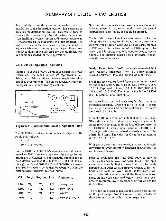
SUMMARY OF FILTER CHARACTERISTICS
described above. As the procedure described performs an addition to the destination location, it is necessary to initialize the destination location. This can be done by clearing the location (e.g., by subtracting the location from itself) or by converting an addition operation to an LDA and placing it as the first step of the sequence. The last steps to realize the filter involve adding the weighted input variable and computing the output. Procedures similar to those above are used for the multiplications and additions needed for these operations.
5.6.1 Simulating Single Real Poles
Figure 5-11 shows a block diagram of a sampled 1 pole realization. The block labeled z-l represents a unit delay, i.e., a delay equivalent to one sample interval or one 2920 program pass. The blocks labeled X represent multiplications, in each case by a constant.
a FREQUENCY
Figure 5-11. Implementation of Single Real Poles
The FORTRAN statements to implement Figure 5-11 b would be as follows:
YI = YO
YO = B*YI + G*X
For the 2920, the FORTRAN statements would be converted to 2920 statements as shown in the section on arithmetic in Chapter 4. For example, suppose it had been determined that B = 0.9922 (B = 0.11111110 in binary) and G = 0.0078125 (G = 0.0000010 in binary). The 2920 instructions could then be generated, using the methods described previously as follows:
OP Dest Source Shift Comments
LDA YI,
LDA YO,
SUB YO,
ADD YO,
YO,
YI,
YI,
x,
ROO ; propagation
ROO ; YO = l.O*YI
R07 ; YO=B*YI
R07 ; YO = B*YI + G*X
5-12
Note that the comments show how the new value of YO is being generated. However, in this case, the second instruction is superfluous, and could be omitted.
Much of the design of such a section consists of determining the best values for Band G that are consistent with meeting of design goals and also are easily realized in 2920 code. It is the function of the 2920 support software to aid in optimizing 2920 code subject to design bounds. The example given below is intended to illustrate the procedures involved.
Design Example No.1-For a sample interval of 76.8 Ilsec., realize a single-pole filter with a time constant (1/0) of 1.50msec ± 1 %, and DC gain of 1.00 ± 1070.
The limits on B can be found from evaluating B = e-oT
for the range 1.485 ~ RC ~ 1.515, i.e., 0.94960 ~ B ~ 0.95057. Expressed in binary, 0.1111001100011000 ~ B ~ 0.1111001101011000. The central value is B = 0.95009 or 0.1111001100111001 in binary.
Any value in the specified range may be chosen to meet the design criterion. A value of B = 0.1111001101 meets the design criterion and can be realized in five steps: B = 20 -2-4 +2-6 _2-8 +2- 1°. From the DC gain equation, note that G = (1-B) ± 1070. Given the value for B above, the range of acceptable values for G, expressed in binary is 0.000011001010 < G < 0.00001100111 with a target value of 0.0000110011. The target value can be realized as easily as any of the others, in 4 steps. The value for G can be expressed as G = 2-4 -2-6 + 2-8 -2-10
With the two constants evaluated, they can be directly converted to 2920 assembly language instructions, as will be shown below.
Prior to evaluating the final 2920 code, it may be necessary to consider overflow possibilities. If the input values are suitably limited, overflow can be made impossible. In other cases, a proper sequence of instructions can at least limit overflow to the last instruction, so that saturation occurs only if the final value is too large. In the code generated below, terms have been ordered to prevent overflow from occurring on any but the last line.
The following sequence realizes the single pole section of Design Example No.1. Comments are included to show the contribution of instruction sequences.
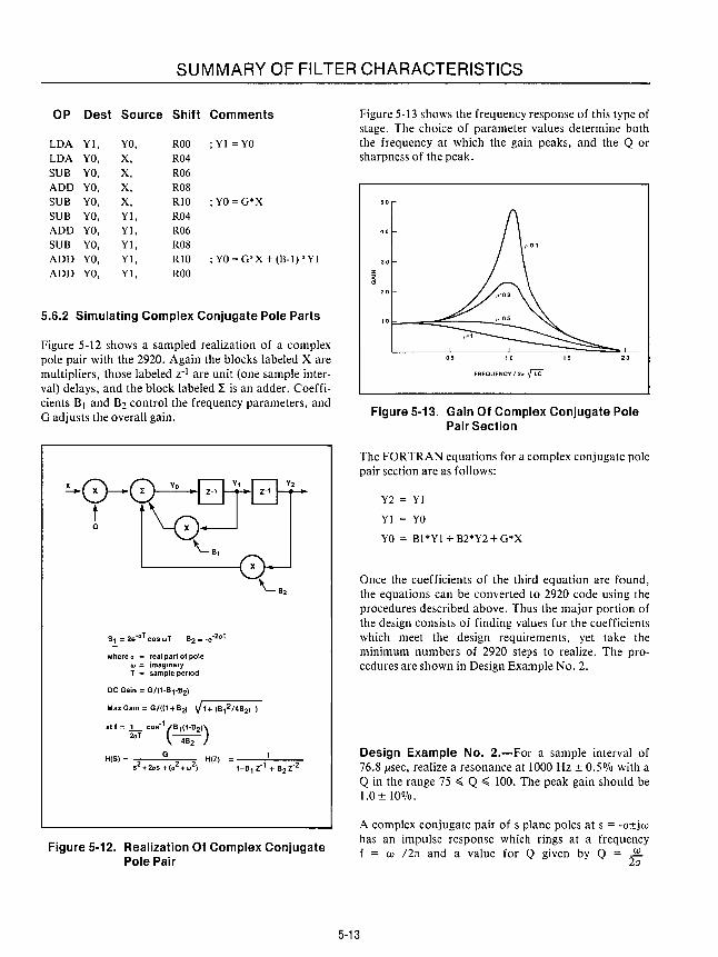
SUMMARY OF FILTER CHARACTERISTICS
OP Dest Source Shift Comments
LOA YI, YO, ROO ;YI =YO LOA YO, X, R04 SUB YO, X, R06 ADD YO, X, R08 SUB YO, X, RIO ; YO = G*X SUB YO, Yl, R04 ADD YO, YI, R06 SUB YO, YI, R08 ADD YO, YI, RIO ; YO = G*X + (B-1) *YI ADD YO, YI, ROO
5.6.2 Simulating Complex Conjugate Pole Parts
Figure 5-12 shows a sampled realization of a complex pole pair with the 2920. Again the blocks labeled X are multipliers, those labeled z-I are unit (one sample interval) delays, and the block labeled L is an adder. Coefficients BI and B2 control the frequency parameters, and G adjusts the overall gain.
x 0-t:\ Yo _~1 J2 - t ~Z-l Z-l
0\0 '-61
X
61 = 2e-oT cos wT 62 = ,e,20T
where 0 = real part 01 pole w = imaginary T = sample period
DC Gain = G/(1,61,62)
Max Gain = G/«1 + 621 V 1 + (612/462) )
atl = L COS,1(61(1,62») 20 T ----:rn;-
H(S) = 2 G 2 2 H(Z) s +20s +(0 +w ) 1-61 Z,1 + 62 Z,2
Figure 5-12. Realization Of Complex Conjugate Pole Pair
5-13
Figure 5-13 shows the frequency response of this type of stage. The choice of parameter values determine both the frequency at which the gain peaks, and the Q or sharpness of the peak.
50
z ;;
"
FREQUENCY I 2rr {LC
Figure 5-13. Gain Of Complex Conjugate Pole Pair Section
The FORTRAN equations for a complex conjugate pole pair section are as follows:
Y2 = YI
YI = YO
YO = BI *YI + B2*Y2 + G*X
Once the coefficients of the third equation are found, the equations can be converted to 2920 code using the procedures described above. Thus the major portion of the design consists of finding values for the coefficients which meet the design requirements, yet take the minimum numbers of 2920 steps to realize. The procedures are shown in Design Example No.2.
Design Example No. 2.-For a sample interval of 76.8 I-lsec, realize a resonance at 1000 Hz ± 0.5070 with a Q in the range 75 ~ Q ~ 100. The peak gain should be 1.0 ± 10070.
A complex conjugate pair of s plane poles at s = -a±jw has an impulse response which rings at a frequency f = w I2rr and a value for Q given by Q = 2~
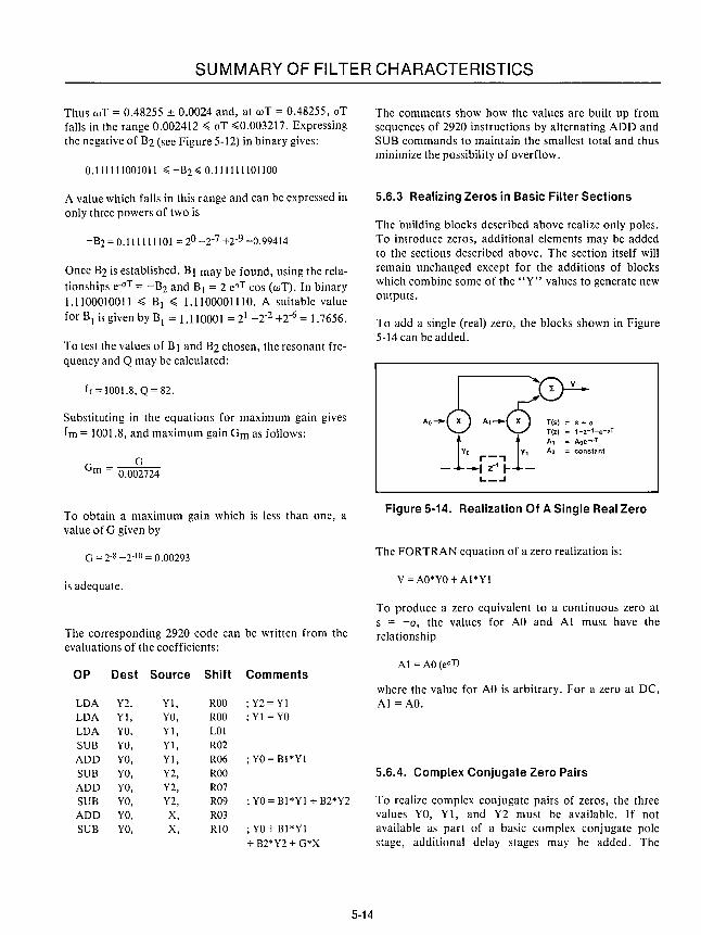
SUMMARY OF FILTER CHARACTERISTICS
Thus wT = 0.48255 ± 0.0024 and, at wT = 0.48255, aT falls in the range 0.002412 ~ aT ~0.003217. Expressing the negative of B2 (see Figure 5-12) in binary gives:
0.111111001011 ~ - B2 ~ 0.11111110 1100
A value which falls in this range and can be expressed in only three powers of two is
Once B2 is established. B1 may be found, using the relationships e-aT = -B2 and Bl = 2 eaT cos (wT). In binary 1.1100010011 ~ BI ~ 1.1100001110. A suitable value
for BI is given by BI = 1.110001 = 21 -2-2 +2-6 = 1.7656.
To test the values of B1 and B2 chosen, the resonant frequency and Q may be calculated:
fr = 1001.8, Q = 82.
Substituting in the equations for maximum gain gives
fm = 1001.8, and maximum gain G m as follows:
G Gm = 0.002724
To obtain a maximum gain which is less than one, a value of G given by
G = 2-8 -2-10 = 0.00293
is adequate.
The corresponding 2920 code can be written from the evaluations of the coefficients:
OP
LDA LDA LDA SUB ADD SUB ADD SUB ADD SUB
Oest Source Shift Comments
Y2, Yl, Yl, YO, YO, YI, YO, YI, YO, YI, YO, Y2, YO, Y2, YO, Y2, YO, X, YO, X,
ROO ROO LOI R02 R06 ROO R07 R09 R03 RIO
; Y2=YI ; YI =YO
; YO = BI*YI
; YO = BI *YI + B2*Y2
;YO+BI*YI + B2*Y2 + G*X
5-14
The comments show how the values are built up from sequences of 2920 instructions by alternating ADD and SUB commands to maintain the smallest total and thus minimize the possibility of overflow.
5.6.3 Realizing Zeros in Basic Filter Sections
The building blocks described above realize only poles. To introduce zeros, additional elements may be added to the sections described above. The section itself will remain unchanged except for the additions of blocks which combine some of the "Y" values to generate new outputs.
To add a single (real) zero, the blocks shown in Figure 5-14 can be added.
Figure 5-14. Realization Of A Single Real Zero
The FORTRAN equation of a zero realization is:
v = AO*YO + Al *YI
To produce a zero equivalent to a continuous zero at s = -a, the values for AO and Al must have the relationship
Al = AO (eaT)
where the value for AO is arbitrary. For a zero at DC, A1=AO.
5.6.4. Complex Conjugate Zero Pairs
To realize complex conjugate pairs of zeros, the three values YO, Y 1, and Y2 must be available. If not available as part of a basic complex conjugate pole stage, additional delay stages may be added. The
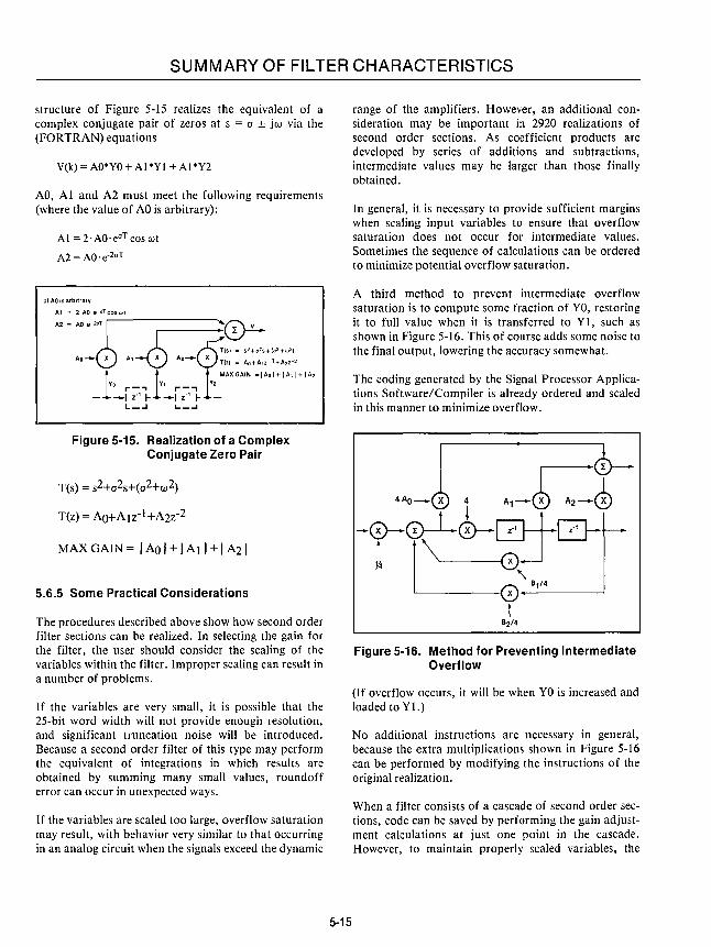
SUMMARY OF FILTER CHARACTERISTICS
structure of Figure 5-15 realizes the equivalent of a complex conjugate pair of zeros at s = a ± jw via the (FORTRAN) equations
V(k) = AO*YO + Al *YI + Al *Y2
AO, Al and A2 must meet the following requirements (where the value of AO is arbitrary):
Al = 2'AO'eoT cos wt
A2 = AO . e-2oT
of AD IS arbitrary
A1 = 2 AD e-oT cos wt
Figure 5-15. Realization of a Complex Conjugate Zero Pair
T(s) = s2+a2s+(a2+w2)
T(z) = AO+AIZ-I+A2Z-2
MAX GAIN = IAol+IAII+IA21
5.6.5 Some Practical Considerations
The procedures described above show how second order filter sections can be realized. In selecting the gain for the filter, the user should consider the scaling of the variables within the filter. Improper scaling can result in a number of problems.
If the variables are very small, it is possible that the 25-bit word width will not provide enough resolution, and significant truncation noise will be introduced. Because a second order filter of this type may perform the equivalent of integrations in which results are obtained by summing many small values, roundoff error can occur in unexpected ways.
If the variables are scaled too large, overflow saturation may result, with behavior very similar to that occurring in an analog circuit when the signals exceed the dynamic
5-15
range of the amplifiers. However, an additional consideration may be important in 2920 realizations of second order sections. As coefficient products are developed by series of additions and subtractions, intermediate values may be larger than those finally obtained.
In general, it is necessary to provide sufficient margins when scaling input variables to ensure that overflow saturation does not occur for intermediate values. Sometimes the sequence of calculations can be ordered to minimize potential overflow saturation.
A third method to prevent intermediate overflow saturation is to compute some fraction of YO, restoring it to full value when it is transferred to Y 1, such as shown in Figure 5-16. This of course adds some noise to the final output, lowering the accuracy somewhat.
The coding generated by the Signal Processor Applications Software/Compiler is already ordered and scaled in this manner to minimize overflow.
Figure 5-16. Method for Preventing Intermediate Overflow
(If overflow occurs, it will be when YO is increased and loaded to YI.)
No additional instructions are necessary in general, because the extra multiplications shown in Figure 5-16 can be performed by modifying the instructions of the original realization.
When a filter consists of a cascade of second order sections, code can be saved by performing the gain adjustment calculations at just one point in the cascade. However, to maintain properly scaled variables, the
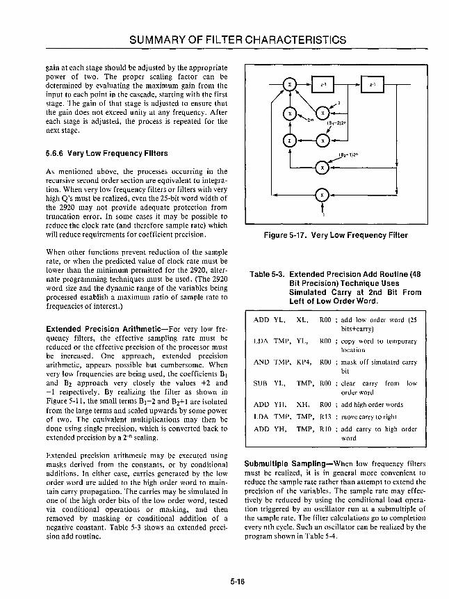
SUMMARY OF FILTER CHARACTERISTICS
gain at each stage should be adjusted by the appropriate power of two. The proper scaling factor can be determined by evaluating the maximum gain from the input to each point in the cascade, starting with the first stage. The gain of that stage is adjusted to ensure that the gain does not exceed unity at any frequency. After each stage is adjusted, the process is repeated for the next stage.
5.6.6 Very Low Frequency Filters
As mentioned above, the processes occurring in the recursive second order section are equivalent to integration. When very low frequency filters or filters with very high Q's must be realized, even the 25-bit word width of the 2920 may not provide adequate protection from truncation error. In some cases it may be possible to reduce the clock rate (and therefore sample rate) which will reduce requirements for coefficient precision.
When other functions prevent reduction of the sample rate, or when the predicted value of clock rate must be lower than the minimum permitted for the 2920, alternate programming techniques must be used. (The 2920 word size and the dynamic range of the variables being processed establish a maximum ratio of sample rate to frequencies of interest.)
Extended Precision Arithmetic-For very low frequency filters, the effective sampling rate must be reduced or the effective precision of the processor must be increased. One approach, extended precision arithmetic, appears possible but cumbersome. When very low frequencies are being used, the coefficients Bl and B2 approach very closely the values +2 and -1 respectively. By realizing the filter as shown in Figure 5-11, the small terms BI-2 and B2+1 are isolated from the large terms and scaled upwards by some power of two. The equivalent multiplications may then be done using single precision, which is converted back to extended precision by a 2-n scaling.
Extended precision arithmetic may be executed using masks derived from the constants, or by conditional additions. In either case, carries generated by the low order word are added to the high order word to maintain carry propagation. The carries may be simulated in one of the high order bits of the low order word, tested via conditional operations or masking, and then removed by masking or conditional addition of a negative constant. Table 5-3 shows an extended precision add routine.
5-16
I_--------~~------------~ t 1
Figure 5-17. Very Low Frequency Filter
Table 5-3. Extended Precision Add Routine (48 Bit Precision) Technique Uses Simulated Carry at 2nd Bit From Left of Low Order Word.
ADD YL, XL, ROO ; add low order word (25 bits+carry)
LDA TMP, YL, ROO ; copy word to temporary location
AND TMP, KP4, ROO ; mask off simulated carry bit
SUB YL, TMP, ROO ; clear carry from low order word
ADD YH, XH, ROO ; add high order words
LDA TMP, TMP, R13 ; move carry to right
ADD YH, TMP, RIO ; add carry to high order word
Submultiple Sampling-When low frequency filters must be realized, it is in general more convenient to reduce the sample rate rather than attempt to extend the precision of the variables. The sample rate may effectively be reduced by using the conditional load operation triggered by an oscillator run at a submultiple of the sample rate. The filter calculations go to completion every nth cycle. Such an oscillator can be realized by the program shown in Table 5-4.
SUMMARY OF FILTER CHARACTERISTICS
Table 5-4. Implementation of Submultiple Sampling
; Oscillator
SUB OSC, KPl, R05, subtract constant KPI fromOSC
LOA DAR, OSC, ROO, move to DAR for sign test
LOA OSC, KP3, ROO, CNDS re-initialize if negative to
ADD OSC, KP3, R05, CNDS ; 99 times KP 1
; conditional filter implementation
LOA Y2, Yl, ROO, CNDS delay occurs only on cycling
LOA Yl, YO, ROO, CNDS ; of oscillator
; remainder of filter calculations are done uncondi; tionally - result is valid only on cycling of oscillator
In the program (Table 5-4) a constant value is subtracted from a RAM location on each pass through the program. If (and only if) that operation causes the result to be negative, the condition for re-initializing the oscillator is met. A conditional LDA (as opposed to conditional ADD in section 4.2) operation restores the oscillator to a positive value. Thus the oscillator cycles at a submultiple of a sample rate (at 1/100 in Table 5-4 ,example.)
The filter itself is realized using the same equations as are used in any second order section, with the exception that the delay realization operations, i.e., loading Yl to Y2 and YO and Yl, are performed only on those progrm passes which re-initialize the oscillator. Because the oscillator calculations only produce re-initialization every nth cycle, a sample rate has been achieved equal to the 2920 sample rate divided by n.
5.6.7 Filters at a Multiple of the Sampling Rate
On occasion, it may be desirable to implement filters at frequencies too high for the basic program sampling rate or to operate one or more stages of the filter at a higher sample rate than that of the 2920. For example, it may be possible to use a lower cost external anti-aliasing filter by sampling the inputs at a higher than normal rate, and performing some of the anti-aliasing using a
5-17
digital filter stage operating at this higher rate. Subsequent processing of the data is performed at the nominal rate of the 2920.
One means for achieving the higher sample rate is to use two copies each of the sampling routine and the antialias digital filter section. Figure 5-18 shows the impact on the external anti-alias requirements obtained by using the double sample rate technique. External antialias requirements may also be reduced for 2920 outputs by the use of interpolating digital filters, i.e., filters which compute values between successive samples.
Interpolating filters may also be realized by operating a filter stage at twice the sample rate by using two copies of the program within the 2920. There are two options for the input of such a filter operating at twice the sample rate. The same input sample may be used for both copies of the program, or one copy may use a zerovalued input. The latter case resembles using an impulse source where the former case is more like a sampled and held source. The Signal Processor Application Software/Compiler can be used to produce code for this mixed sample rate implementation. The methods produce somewhat different frequency responses.
5.6.8 Other Filter Structures
In most of the examples described above, a cascade of filter stages has been assumed. However, when the impulse invariant transform is used, an alternate realization could be found by expanding into a sum of partial fractions, evaluating the impulse response associated with each fraction, and realizing the output of the filter as the sum of the section outputs. The resulting realization is shown in Figure 5-19b as opposed to the cascade structure of Figure 5-19a. In some cases, the parallel structure may be less sensitive to variable scaling than the cascade structure.

SUMMARY OF FILTER CHARACTERISTICS
EXTERNAL ANTI·ALlAS
I r<;j" BW 's·BW
a. Original spectrum showing bandwidth of digital processing. External anti-alias filter must pass below BW, stop beyond fs-BW
1
EXTERNAL ANTI·ALlAS FILTER
,~L INTERNAL DIGITAL FILTER
b. Spectrum using double rate sampling.
21 5
External filter passes BW, stops beyond 2fs-BW, internal digital filter performs rest of anti-alias function.
Figure 5-18. Effects of Double Rate Input Sampling
~:~ :~
~. 1. 8~. Figure 5·19a. Cascade Structure for Complex Filter
(Directly Derived from Matched Z or Bilinear Transform)
5-18
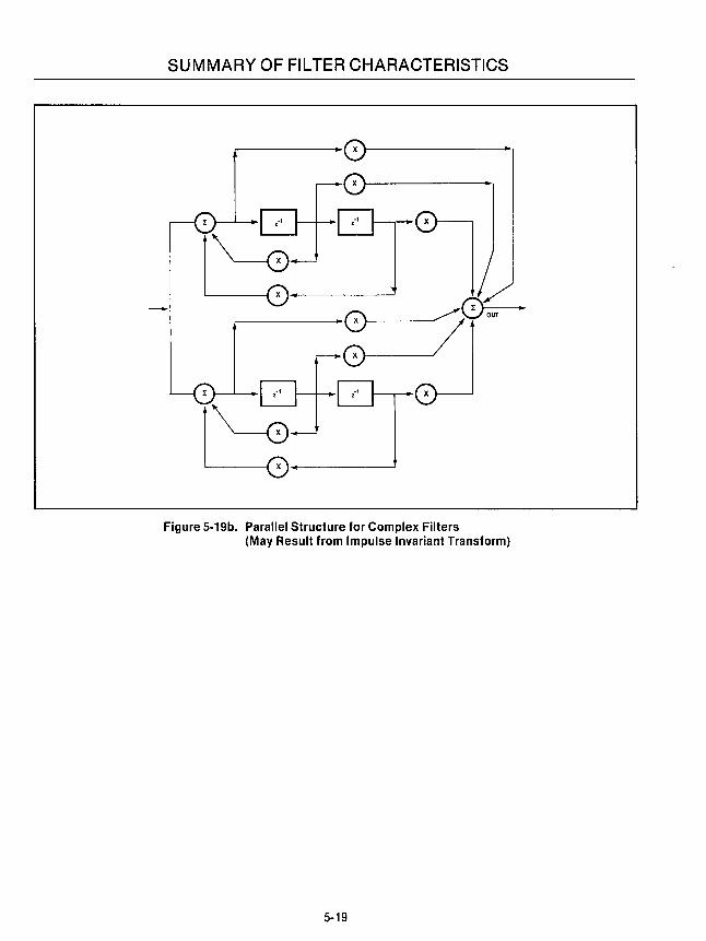
SUMMARY OF FILTER CHARACTERISTICS
0 .
- '0~0S--
Figure 5·19b. Parallel Structure for Complex Filters (May Result from Impulse Invariant Transform)
5·19


Advanced Techniques 6

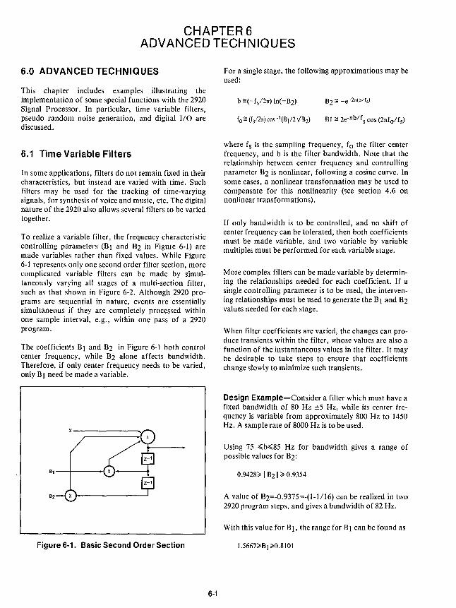
CHAPTER 6 ADVANCED TECHNIQUES
6.0 ADVANCED TECHNIQUES
This chapter includes examples illustrating the implementation of some special functions with the 2920 Signal Processor. In particular, time variable filters, pseudo random noise generation, and digital I/O are discussed.
6.1 Time Variable Filters
In some applications, filters do not remain fixed in their characteristics, but instead are varied with time. Such filters may be used for the tracking of time-varying signals, for synthesis of voice and music, etc. The digital nature of the 2920 also allows several filters to be varied together.
To realize a variable filter, the frequency characteristic controlling parameters (Bl and B2 in Figure 6-1) are made variables rather than fixed values. While Figure 6-1 represents only one second order filter section, more complicated variable filters can be made by simultaneously varying all stages of a multi-section filter, such as that shown in Figure 6-2. Although 2920 programs are sequential in nature, events are essentially simultaneous if they are completely processed within one sample interval, e.g., within one pass of a 2920 program.
The coefficients Bl and B2 in Figure 6-1 both control center frequency, while B2 alone affects bandwidth. Therefore, if only center frequency needs to be varied, only Bl need be made a variable.
x ----------,
Figure 6-1. Basic Second Order Section
6-1
For a single stage, the following approximations may be used:
B2 ~ -e -2n(b/fsl
Bl ~ 2e-nb/fs cos (2nfo/fs)
where fs is the sampling frequency, fo the filter center frequency, and b is the filter bandwidth. Note that the relationship between center frequency and controlling parameter B2 is nonlinear, following a cosine curve. In some cases, a nonlinear transformation may be used to compensate for this nonlinearity (see section 4.6 on nonlinear transformations).
If only bandwidth is to be controlled, and no shift of center frequency can be tolerated, then both coefficients must be made variable, and two variable by variable multiples must be performed for each variable stage.
More complex filters can be made variable by determining the relationships needed for each coefficient. If a single controlling parameter is to be used, the intervening relationships must be used to generate the B 1 and B2 values needed for each stage.
When filter coefficients are varied, the changes can produce transients within the filter, whose values are also a function of the instantaneous values in the filter. It may be desirable to take steps to ensure that coefficients change slowly to minimize such transients.
Design Example-Consider a filter which must have a fixed bandwidth of 80 Hz ±5 Hz, while its center frequency is variable from approximately 800 Hz to 1450 Hz. A sample rate of 8000 Hz is to be used.
Using 75 ~b~85 Hz for bandwidth gives a range of possible values for B2:
0.9428~ 1 B21 ~ 0.9354
A value of B2=-0.9375=-(1-1/16) can be realized in two 2920 program steps, and gives a bandwidth of 82 Hz.
With this value for B 1, the range for B 1 can be found as
1.5667~Bl ~0.8101
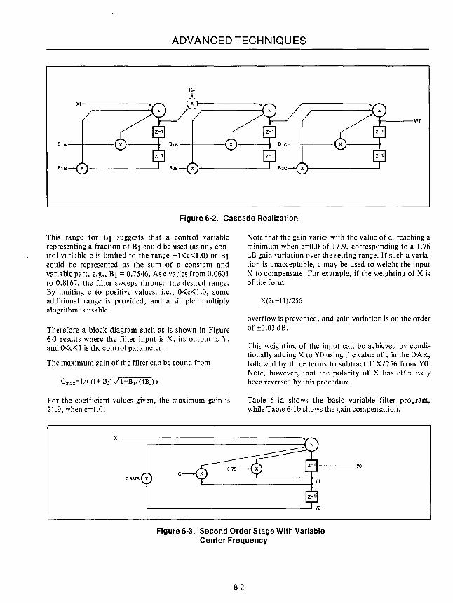
ADVANCED TECHNIQUES
Xl-------___.._ .....
.......---WT
B1A--t----
Figure 6-2. Cascade Realization
This range for BI suggests that a control variable representing a fraction of BI could be used (as any control variable c is limited to the range -1~c<1.0) or BI could be represented as the sum of a constant and variable part, e.g., BI = 0.7546. As c varies from 0.0601 to 0.8167, the filter sweeps through the desired range. By limiting c to positive values, i.e., O~c~ 1.0, some additional range is provided, and a simpler multiply alogrithm is usable.
Therefore a block diagram such as is shown in Figure 6-3 results where the filter input is X, its output is Y, and O<c~ 1 is the control parameter.
The maximum gain of the filter can be found from
For the coefficient values given, the maximum gain is 21.9, when c=1.0.
Note that the gain varies with the value of c, reaching a minimum when c=O.O of 17 .9, corresponding to a 1.76 dB gain variation over the setting range. If such a variation is unacceptable, c may be used to weight the input X to compensate. For example, if the weighting of X is of the form
X(2c-ll)1256
overflow is prevented, and gain variation is on the order of ±0.03 dB.
This weighting of the input can be achieved by conditionally adding X to YO using the value of c in the DAR, followed by three terms to subtract IIX1256 from YO. Note, however, that the polarity of X has effectively been reversed by this procedure.
Table 6-la shows the basic variable filter program, while Table 6-1 b shows the gain compensation.
x---------------------~. __
I-----YO
c
Figure 6-3. Second Order Stage With Variable Center Frequency
6-2
ADVANCED TECHNIQUES
Table 6-1a. Variable Frequency Filter Stage
program for variable frequency filter input is X,output YO, intermediate values Y I, Y2 BI =0.75 +C
B2 is realized by successive additions/subtractions, and value -0.9375 corresponding to a bandwidth of approximately 82Hz when the sample rate is 8KHz.
propagate through delay stages LDA Y2, YI, ROO LOA Y I YO, ROO
; generate B2*Y2 in YO LOA YO, Y2, R4 SUB YO, Y2, RO
; set up for mUltiply LOA DAR, C, RO
; perform multiply and add to YO ADD YO, YI, RI, ADD YO, YI, R2, ADD YO, YI, R3, ADD YO, YI, R4, ADD YO, YI, R5, ADD YO, YI, R6, ADD YO, YI, R7, ADD YO, YI, R8,
CND7 CND6 CND5 CND4 CND3 CND2 CNDI CNDO
; add 0.75*YI to YO to complete BI *YI ADD YO, YI, RI ADD YO, Yl, R2
; +1I16*Y2 in YO ; -15/16*Y2 in YO
add in input to filter, scaled to prevent overflow ADD YO, YI, R5
; filter range is 569 to 1493 Hz center frequency, resolution is 6 Hz at 569,3 Hz at 1493
Table 6-1b. Gain Compensation
in place of the last code line of table 6-la, which added in the input scaled to avoid overflow, the gain compensation code below can be substituted:
Gain compensation-add x(c/128) ADD YO, X, R8, CND7 ADD YO, X, R9, CND6 ADD YO, X, RIO, CND5 ADD YO, X, RII, CND4 ADD YO, X, R12, CND3 ADD YO, X, R13, CND2
; Subtract X* 111256 = X(l/32 + 11128 + 11256) SUB YO, X, R5 SUB YO, X, R7 SUB YO, X, R8
Note-only 7 bits precision were used in the multiplication by c, to prevent the need for additional temporary RAM locations
6-3
ADVANCED TECHNIQUES
6.2 Noise Generation With The 2920
Some signal processing applications call for a source of noise. A noise generator may be modeled by a pseudorandom number generator. The 2920 realization shown in Table 6-2 is implemented by a feedback shift register, using only one variable location. The shift operation is realized by loading the number to itself shifted appropriately. The exclusive-or operation (XOR) is used to generate the bit to be entered into the shift register which is done by the addition operation.
6.3 Digitallnput/Output
If parameters used in the 2920 need to be transferred on or off the chip, an analog voltage is the natural way to represent the parameter. An example has been shown for a voltage controlled variable frequency oscillator. However, in many applications, the source or receiver of the parameter requires a digital representation. Various signals in and out of the 2920 and its processing power can be used to provide digital 110. This section will describe some of the techniques, important issues in the choice of techniques and some examples.
A variety of methods are useful for digital 110. The choice will depend on knowing some of the following for your application; The maximum data rate, how many bits per second, per sample period, or per program pass? Some methods are faster in continuous bit rate. How often does data change? Can a buffer and a slow data rate be used because the data changes infrequently? What is the natural format of the data; bit serial or parallel, for example? What controls the transfer? Is the 2920 the master or the slave in the 110 process? Is the transfer synchronous or nonsynchronous with the 2920 program execution? What resources are available on the 2920 for digital 110 after the main function has been accomplished; how many SIGIN or SIGOUT pins are free? How much program space is available for digital 110 or what is the composition of the main program; is it easier to add more digital or more analog instructions?
Typically an I/O transfer has the data bit representing a binary one or zero, a clock or activating signal and one or more control signals. The resources on the 2920 for possible use in these three functions are:
SIGIN(K). These four pins provide the only possible inputs (other than the RESET which is useful only for the control function). A sequence of IN(K) and CVT(K)
Table 6-2. Noise Generator Routine
; Random noise generator using feedback shift register.
; Register length is 17 bits. ; First test for all zeros condition-ensure proper start. ; TEMP is temporarily used variable, NGEN is generator output.
LDA SUB LDA LDA
TEMP, TEMP, DAR, TEMP,
NGEN, KP1, TEMP, KP4,
Ll R13
CNDS
; Next fetch the 17th bit, test and move to DAR
LDA AND SUB LDA
TEMP, TEMP, TEMP, DAR,
KP1, NGEN, KP1, TEMP
R13 Ll R13
; test subtraction, negative result implies need for initialization; move to DAR for sign test, init if neg.
; Test subtraction to convert bit to sign; set DAR to + 1.0 for 1, ; -1.0 for 0
Next bit of shift register is XOR of bits 17 and bit 5
XOR DAR, NGEN
Shift register right, and fill in new value
LDA ADD
NGEN, NGEN,
NGEN, KP4,
Rl CNDS
; generate in DAR
shift right
6-4

ADVANCED TECHNIQUES
instructions put the input bit in the DAR. The maximum input rate is determined by the size of the input sample and hold capacitor. The threshold between a zero and a one can be set anywhere between 0 and ± VREF by what is initially in the DAR.
SIGOUT (K). These eight outputs can provide a logical one and zero at any two voltage levels between ± VREF with a load DAR and OUT (K) sequence. Open drain TTL levels are possible in groups of four output pins controlled by MI and M2 if VREF~ 1.5 volts. External pull-up resistors should be used. Speed is the same for either analog or TTL output mode.
OF. This open drain output provides a high speed TTL output which may be set or cleared with a single instruction.
CCLK. This open drain clock signal which occurs every four instruction executions, although always present, provides a convenient activating signal for digital I/O transfers.
RST /EOP. As an open drain output the EOP is a convenient clock or control signal for transfers which occurs only once per program pass. RST can be a nonsynchronous control input when gated with CCLK.
Each complete 110 operation may consist of four different operations; a control sequence, a data assembly or put-away sequence, a data transfer sequence and a clocking or activation sequence. Specific examples are given using the different inputs and outputs on the 2920. The examples are not exhaustive but they show some representative sequences for the four functions in a complete 110 operation.
Output Parallel-For synchronous parallel output of one byte (8 bits) per program pass with the 2920 as master (see Figure 6-4). Table 6-3 shows the instruction sequence.
Table 6-3. Digital Output: Parallel
Instruction Sequence.
LDA
LDA
LDA LDA
LDA LDA
OUT7
LDA
OUTO
Summary:
DAR, DATA
D7, KPO
DO, KPO D7, KP7,
DO, KP7, DAR, D7
DAR, DO
Analog instructions Digital instructions Input pins Output pins Data memory locations Overflow
CND7
CNDO
8 +8B* 17 o 8 8
Load output byte into DAR
Initialize Data buffers
DO-D7 to zero.
Load +FS to data buffers
if tested bit = I
Output Data buffers
DO-D7 on Outputs 0-7
Not affected
*B equals the number of analog NOP and OUT instructions needed for the device and clock rate used. See Chapter 3 for analog design rules.
6-5

ADVANCED TECHNIQUES
+5V
5.6k
+2V VREF SIGOUT 7
07
M2 2920
74364
~ REGISTER
SIGOUT 0
+5V
DO
DATA OUT
1\
lEap I CLOCK
Figure 6·4. Logic Diagram for Digital Output: Parallel
With a 10 MHz clock and B=5, the total of 65 instructions for output would provide a maximum of 38 K bytes/second transfer rate. With a full length program this would be reduced by a factor of three.
Output Serial-For synchronous parallel output of one byte using serial transfer out of the 2920 overflow (OF) pin. Multiple bytes per program pass can be outputted with the 2920 as master and one control signal, (see Figure 6-5). Table 6-4 shows the instruction sequence.
Table 6·4. Digital Output: Serial
Instruction Sequence.
Instruction sequence.
LDA DAR, KP7
OUTO
LDA DAR, DATA 3 LDA R, KPO 0 LDA R, KP4, 1 NOP 2 LDA R, R,
LDA R, KPO LDA R, KP4, LDA DAR, KPO LDA R, R,
OUTO
Summary:
Analog instructions Digital instructions Input pins Output pins Data memory location Overflow
Set DATA VALID
Load byte of data into DAR Set R = 0
CNDO R=O.5 if data bit 0 is 1
L2 Overflow if bit 0 was 1
Repeat sequence through bit 7 CND7
L2 Overflow if bit 7 was 1
Clear DATA VALID
8+2B 19 o 1 1
Affected during I/O
6-6

ADVANCED TECHNIQUES
5.6kQ +5V-----...---.---'VI./v-----,
DATA
+2V VREF
74164 2920 SHIFT
REGISTER M1 SIG OUT 0
+5V-
CLOCK
~-------------~~
Figure 6-5. Logic Diagram for Digital Output: Serial
With a 10 MHz clock a transfer rate of 55 K Bytes per second is obtained for each instruction sequence or as high as 220 K Bytes/second per program pass.
Note that the clocking by CCLK requires that the overflowing instruction be located as shown in the diagram. The CCLK signal will occur during instructions which are a multiple of four. The conditional test on the data and the potential overflow must be done with two separate instructions. A conditional overflow instruction will assert OF even if the condition is not met. (Figure 6-6)
Overflows may occur during other portions of the program since there will be no clocking of the shift register.
OVERFLOW DURING INSTRUCTION 2
Input Parallel-For synchronous parallel input of one byte per program pass with the 2920 as master. Table 6-5 shows the instruction sequence.
With a 10 MHz clock a transfer rate of 37.5 K Byte/sec is obtained for each instruction sequence which is once per program pass if the EOP is used for the control signal.
This method uses all analog input pins, often an unacceptable'demand. Using fewer pins slows the data rate only slightly since the majority of the time is spent in sampling and converting rather than data manipulation. (See Figure 6-7.) Table 6-5 shows the instruction sequence.
INSTRUCTION
TIME~
Figure 6-6. Timing Diagram
6-7

ADVANCED TECHNIQUES
Table 6-5. Digital Input: Parallel
Instruction Sequence.
LOA DAR, KP7
OUT 0
LOA DAR, KP2 IN3
CVT3
INO
CVTO SUB DAR, KP2 LOA 0, DAR,
DOA, 0, LOA DAR, KPO
aUTO
LOA DAR, KP2 IN3
CVT3
INO
CVTO SUB DAR, KP2 XOR 0, DAR
Summary:
Analog instructions Digital instructions Input pins Output pins Data memory locations Overflow
L2 L2
Select higher order four bits
Load DAR + FS/4 Input Bit 3
Convert Bit 3
Repeat through Bit 0
DAR contains four higher order bits MSB's
Left shift DAR four bits and store in 0
Select lower order
four bits.
Load DAR FS/4
DAR contains four lower order bits Combine high and low order bits
SA + 2B + 8C* 9 4 I I
Not affected
* A equals the number of IN instructions and C equals the CVT and NOP instruction needed for the device and clock rate used. See Chapter 3 for analog design rules.
6-8

ADVANCED TECHNIQUES
07
DATA IN
DO
DATA TAKEN
SELECT I
4Y • · · . · 74157 . · · · 1Y • ISTROBE
...L
+5V
1.5k
15k
~'"
l 56kQ
SIGIN 3
. . SIGIN 0
2kQ
1 I
IEOP
2920
SiG'OliTo
VREF -~
56K
+2V
+5V
Figure 6-7. Logic Diagram for Digital Input: Parallel
Input Parallel-Serial-This example reduces the number of analog inputs committed to digital parameters yet accepts parallel loads. The transfer is synchronous with the 2920 as master and multiple bytes can transfer per program pass (see Figure 6-8). Table 6-6 shows the instruction sequence.
T LOAD} 1 CLOCK INHIBIT
DATATAKEN LOAD DATA
SERIAL 1.5kQ 07 -. OUT
: 74165 : DATA IN
DO -ICLOCK
With a 10 MHz clock a transfer rate of 30K Bytes/sec is obtained for the instruction sequence or up to twice that amount per full program pass.
+5V
SIGIN 0
2.kQ
-=
5.6kQ
~O 2920 SIGOUT 1
• VREF
M1
lOF
+2V
+5V
Figure 6-8. Logic Diagram for Digital Input: Parallel-Serial
6-9
ADVANCED TECHNIQUES
Table 6-6. Digital Input: Parallel-Serial
Instruction Sequence.
LDA D, KPO LDA DAR, KPO
aUTO Enable parallel load
OUTl Enable clock LDA DAR, KP7 Clear parallel load
aUTO
LDA DAR, KP2 DAR = FS/4
INO Input D7
CVT3
LDA R, KP7, Ll OF clocks shift register INO Input D6
CVT2 LDA R, KP7, Ll Repeat through D4
CVTO LDA R, KP7, Ll SUB DAR, KP2 DAR contains 07-04 LDA 0, OAR, L2 Left shift OAR two bits into D LOA OAR, KP2 Repeat for 03-00
INO
CVT3 LDA R, KP7, Ll
CVTO SUB DAR, KP2 DAR contains 03-00 XOR DAR, D, L2 OAR contains 00-07 LOA D, DAR Load 07-00 into D LOA OAR, KP7
OUTl Disable clock Summary:
Analog instructions 8A+3B+8C Oigital instructions 19 Input pins I Output pins 2 Oata memory locations 2 Overflow Affected
6-10
ADVANCED TECHNIQUES
BYTE TAKEN
DATA TAKEN
SERIAL DATA IN
DATA READY
1.SK
1.SK
SIGIN 0
SIGIN 1
2K
-'-
SIGOUT 0
SIGOUT 1
2920 VREF • M1
1 +2V
+5V
Figure 6-9. Logic Diagram for Digital Input: Serial
Input Serial-This example illustrates nonsynchronous inputs on a bit serial basis with one bit per program pass and multiple bytes put away in the 2920 (see Figure 6-9). Table 6-7 shows the instruction sequence.
The BYTE TAKEN signal may be used for BYTES TAKEN by having it asserted on the reset of CT2 rather than CTI.
Transfers Between Two 2920's-When two or more 2920's are used together digital parameters may need to be passed between them. The obvious method would seem to be to output an analog representation of the
IOF
2920 #1
X1y21 I EOP
1 EXT elK ExTCLi<
S.6K
number which is converted back in the receiving 2920. This method is limited to about four bits per transfer because the effective gain between an output and an input is approximately 0.9. Generally fewer instructions and/or greater speed result if the overflow is used for outputting and one bit conversion made on input. The input analog sample time is reduced if only a binary decision is made and the lengthy output sequence is avoided with the use of the overflow pin.
The previous examples of serial output and input may be used for the program sequence. Synchronism of the two programs is assured within seven instructions by the paralleled EOP signals and use of the same external clock. Exact synchronization is possible with external logic. (See Figure 6-10.)
T +sv
3.3K
SIGIN 0
2920 2K #2
~ +2V
~
xllx2T 1 EOP
I I
Figure 6-10. Synchronizing Multiple 2920s
6-11
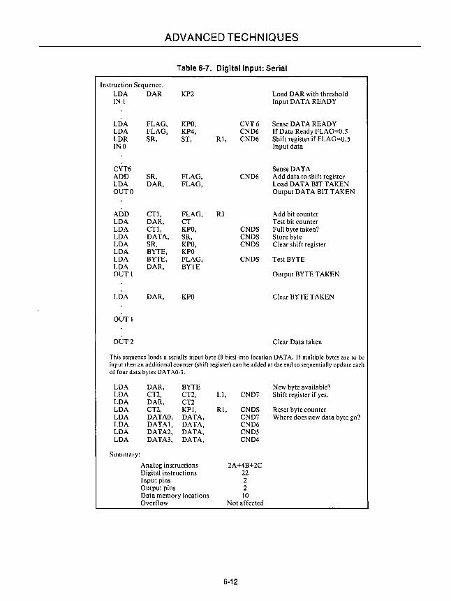
ADVANCED TECHNIQUES
Table 6-7. Digital Input: Serial
Instruction Sequence. LDA DAR INI
LOA LOA LDR INO
CVT6 ADD LOA OUTO
ADD LOA LOA LOA LOA LOA LOA LOA OUT I
LOA
OUTI
OUT2
FLAG, FLAG, SR,
SR, DAR,
CT!, DAR, CT!, DATA, SR, BYTE, BYTE, DAR,
DAR,
KP2
KPO, KP4, ST,
FLAG, FLAG,
FLAG, CT KPO, SR, KPO, KPO FLAG, BYTE
KPO
RI,
R3
CVT6 CND6 CND6
CND6
CNDS CNDS CNDS
CNDS
Load DAR with threshold Input DATA READY
Sense OAT A READY If Data Ready FLAG=O.5 Shift register if FLAG=O.5 Input data
SenseDATA Add data to shift register Load DATA BIT TAKEN Output DATA BIT TAKEN
Add bit counter Test bit counter Full byte taken? Store byte Clear shift register
Test BYTE
Output BYTE TAKEN
Clear BYTE TAKEN
Clear Data taken
This sequence loads a serially input byte (8 bits) into location DATA. If multiple bytes are to be input then an additional counter (shift register) can be added at the end to sequentially update each of four data bytes DAT AO-3.
LOA DAR, BYTE New byte available? LOA CT2, CT2, Ll, CND7 Shift register if yes. LOA DAR, CT2 LOA CT2, KPI, RI, CNDS Reset byte counter LOA DATAO, DATA, CND7 Where does new data byte go? LOA DATAl, DATA, CND6 LOA DATA2, DATA, CND5 LOA DATA3, DATA, CND4
Summary:
Analog instructions 2A+4B+2C Digital instructions 22 Input pins 2 Output pins 2 Data memory locations 10 Overflow Not affected
6-12

Application Examples 7

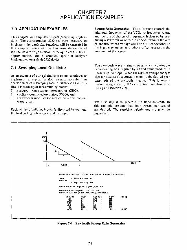
CHAPTER 7 APPLICATION EXAMPLES
7.0 APPLICATION EXAMPLES
This chapter will emphasize signal processing applications. The corresponding 2920 software necessary to implement the particular functions will be generated in this chapter. Some of the functions demonstrated include waveform generation, filtering, piecewise linear approximation, and a complete spectrum analyzer implemented on a single 2920 device.
7.1 Sweeping Local Oscillator
As an example of using digital processing techniques to implement a typical 'analog circuit, consider the development of a sweeping local oscillator (SLO). This circuit is made up of three building blocks: 1) a sawtooth wave sweep rate generator, (SRG), 2) a voltage-controlled oscillator, (VeO), and 3) a waveform modifier (to reduce harmonic content
of the yeO).
Each of these building blocks is discussed below, and the final coding is developed and displayed.
AMP
1.0
I fool .1t----'1.sEC---~·1
Sweep Rate Generator-This subsystem controls the minimum frequency of the yeO, its frequency range, and the rate of change of frequency. It does so by producing a sawtooth wave whose slope determines the rate of change, whose voltage excursion is proportional to the frequency range, and whose offset represents the minimum of that range.
The sawtooth wave is simple to generate: continuous decrementing of a register by a fixed value produces a linear negative slope. When the register voltage changes sign (crosses zero), a constant equal to the desired peak amplitude of the sawtooth is added. This is accomplished using a load (LDA) instruction conditioned on the sign bit (Section 4.2).
The first step is to generate the slope constant. In this example, assume that four sweeps per second are desired. The resulting calculations are given in Figure 7-1.
TIME
ASSUME 1= 76.8 USEC (192 INSTRUCTIONS AT A 10 MHz CLOCK RATE)
THEN 51 = lIT = 1.2288' 10.3 IN BINARY
51 = [0.10100001]' 2.11
WHICH EQUALSsl = [(0.101 + (0.001)'2.5]'2.11
REWRITTEN AS sl = [KP5 + KPl '2.5]'2.11 WHICH, IN 2920 ASSEMBLY LANGUAGE, IS WRITTEN
OPCODE DEST SOURCE ~ sr--; ~
ADD Sl KPl LOA Sl Sl SUB Hl Sl LOA DAR: Hl ADD Hl KP4
SHIFT COND ROO R05 Rll ROO ROO LOl CNDS
Figure 7-1. Sawtooth Sweep Rate Generator
7-1
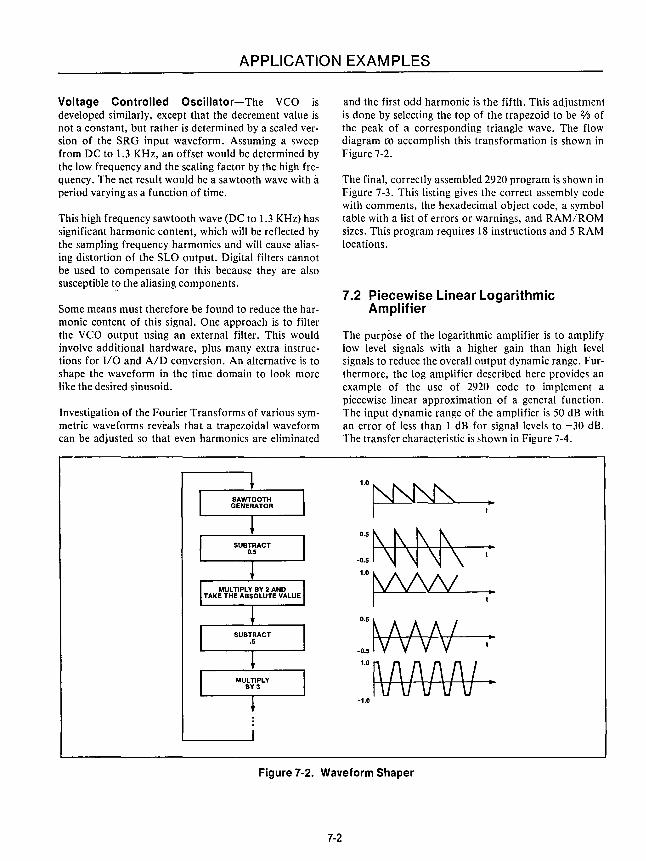
APPLICATION EXAMPLES
Voltage Controlled Oscillator-The VCO is developed similarly, except that the decrement value is not a constant, but rather is determined by a scaled version of the SRG input waveform. Assuming a sweep from DC to 1.3 KHz, an offset would be determined by the low frequency and the scaling factor by the high frequency. The net result would be a sawtooth wave with a period varying as a function of time.
This high frequency sawtooth wave (DC to 1.3 KHz) has significant harmonic content, which will be reflected by the sampling frequency harmonics and will cause aliasing distortion of the SLO output. Digital filters cannot be used to compensate for this because they are also susceptible t? the aliasing components.
Some means must therefore be found to reduce the harmonic content of this signal. One approach is to filter the veo output using an external filter. This would involve additional hardware, plus many extra instructions for 110 and A/D conversion. An alternative is to shape the waveform in the time domain to look more like the desired sinusoid.
Investigation of the Fourier Transforms of various symmetric waveforms reveals that a trapezoidal waveform can be adjusted so that even harmonics are eliminated
and the first odd harmonic is the fifth. This adjustment is done by selecting the top of the trapezoid to be 2/3 of the peak of a corresponding triangle wave. The flow diagram to accomplish this transformation is shown in Figure 7-2.
The final, correctly assembled 2920 program is shown in Figure 7-3. This listing gives the correct assembly code with comments, the hexadecimal object code, a symbol table with a list of errors or warnings, and RAM/ROM sizes. This program requires 18 instructions and 5 RAM locations.
7.2 Piecewise Linear Logarithmic Amplifier
The purpose of the logarithmic amplifier is to amplify low level signals with a higher gain than high level signals to reduce the overall output dynamic range. Furthermore, the log amplifier described here provides an example of the use of 2920 code to implement a piecewise linear approximation of a general function. The input dynamic range of the amplifier is 50 dB with an error of less than 1 dB for signal levels to -30 dB. The transfer characteristic is shown in Figure 7-4.
'5~" " " I -0.5 V'VVV
-t
..
.. t
..
1.0 rJ\/\I\I\J . -1.0
Figure 7-2. Waveform Shaper
7-2
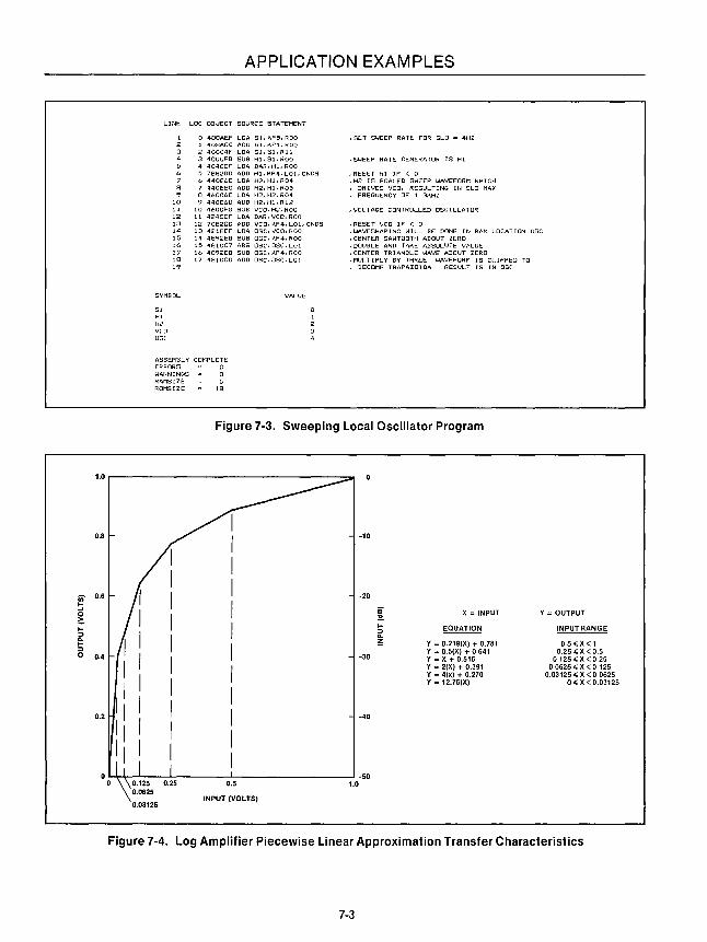
en !:i 0 ~ ..... :::) Q. ..... :::)
0
APPLICATION EXAMPLES
LINE LOC OBJECT SOURCE STATE"MENT
o 488AEF LOA SI. KP5. ROO 2 1 400A8C ADD 51. KP 1. RO:} 3 2 40004F LOA SI. SI. RII 4 3 4000FB SUB HI. SI. ROO 5 4 404CCF LOA DAR. HI. ROO 6 :5 788200 AOD HI. KP4, LOt, eNDS 7 6 44086E LOA H2. HI. R04 8 7 44088C ADD H2. HI. R05 9 8 46006E LOA H2. H2. R04
10 9 440860 ADD H2. HI. RI2 II 10 4600~B SUB VCO. H2. ROO 12 II 424CEF LOA DAR. VCO. ROO 13 12 7C82DD ADD VCO. KP4. LOI. CNDS 14 13 421BE'F LOA OSC. VCO. ROO 15 14 4B92EB SUB OSC. KP4. ROO 16 15 4BIOC7 ABS OSC. OSC. LOI 17 16 4B92EB SUB OSC. KP4. ROO IB 17 4BIOCD ADD OSC. OSC. LOI 19
SYrlBOL VALUE
51 HI H.! V(ll ose
ASSEMBLY COMPLETE ERRORS 0 WARNINGS RAMSIZE ROMSIZE 18
• SeT SWEEP RATE FOR SLo = 4HZ
• SWEEP RATE GENERATOR IS HI
• RESET HI IF ( 0 • H2 IS SCALED SWEEP WAVE"FORM WHICH • DRIVES VCO. RESULTING IN SLO MAX • FREGUENCY OF 13KHZ
• VOLTAGE CONTROLLED OSCILLATOR
• RESET VCO IF ( 0 • WAVESHAPING WILL BE DONE IN RAM LOCAl ION OSC • CENTER SAWTOOTH ABOUT ZERO • DOUBLE AND TAKE ABSOLUTE VALUE • CENTER TR IANCLE WAVE ABOUT ZERO • MULTIPLY BY THREE WAVEFORM IS CLIPPED TO • BECOME TRAPAZOIDAL RESULT IS IN OSC
Figure 7-3. Sweeping Local Oscillator Program
1.0 r---------------------~
O.B -10
0.6 I -20
I I I 0.4 I I
II I I
0.2 II I I: I
! X = INPUT Y = OUTPUT
..... EQUATION INPUT RANGE :::) Q.
~ Y 0.219(X) + 0.781 05 .. X<1
-30 Y 0.5(X) + 0 641 0.25 .. X< 0.5 Y X + 0.516 0125" X < 025 Y 2(X) + 0.391 o 0625 " X < 0 125 Y 4(x) + 0.270 0.03125" X < 00625 Y 12.75(X) 0" X < 0.03125
-40
0.5
0.03125 INPUT (VOLTS)
Figure 7-4. Log Amplifier Piecewise Linear Approximation Transfer Characteristics
7-3

APPLICATION EXAMPLES
Six linear sections are used to approximate the log amplifier. The equations for these sections and the range of inputs for which each equation used are given in Figure 7-4. The equations were obtained graphically, and then adjusted for coding efficiency. The input for the log amplifier must be positive and less than or equal to 1 V. To simplify matters, the endpoints for the linear sections were chosen as powers of two. This way, only one bit of the number to be processed need be checked to determine whether that number falls within an input range. The constant multipliers (slopes) of the linear sections were chosen to minimize error while at the same time allowing the multiplications to be efficiently handled in 2920 code.
The outputs for the log amplifier are also less than or equal to 1 V, and positive. An output of 1 V corresponds to 0 dB, 0.8V to -10 dB, 0.6V to -20 dB, and so on. An output of OV corresponds to -50 dB or below. For example, for a device with a maximum output of 1 V, an output of 0.7V indicates a signal level of -15 dB. Regardless of VREF., a 2920 output which is 70 percent
***LOG AMP*****
of full scale represents -15 dB. Any DC offset which may exist at the output of the part should be taken into account when interpreting the output in dB.
The equations used in the log amplifier program are shown in Figure 7-4, and the assembly code is given in Figure 7-5. The first linear section of the amplifier to be implemented is the sixth section, which corresponds to inputs less than 1 132V. However, all input signals, regardless of amplitude, are processed by the equation for this section initially. The original signal is then placed in the DAR. All the following operations are conditional, and are performed only if the tested bit of the DAR is a "one". Otherwise, a NOP is performed. Each bit of the DAR is tested, starting with bit 3 and progressing to bit 7. When a "one" is located, the multiplier and offset corresponding to the indicated range of the output are used to compute the result. This result replaces any previously computed result. If no "ones" are encountered, the input is less than 1I32V, and only NOP's are performed. The value computed for the sixth section then remains unmodified. Since the
ABS XO. XO, ROO ,PREVENT PROCESSING OF NEGATIVE NUMBERS
, SECTION 6
LDA LOUT, XO, L02 ADD LOUT, XO, LO.:! ADD LOUT, XO, L02 ADD LOUT, XO, RO I ADD LOllT, XO. R02
LDA DAR, XO, ROO
, SECTION 5
LDA LOUT, XO, L02, CND3 ADD LOUT, KP2, ROO, CND3 ADD LOUT. KP5, ROS, CND:3
, SECTION 4
LDA LOUT, XO, LOI, CND4 ADD LOUT. KP3, ROO, CND4 ADD LOUT. KP2, R04, CND4
, SECTION:3
LDA LOUT, XO, ROO, CND5 ADD LOUT, KP4, ROO, CND~ ADD LOUT, KP2, R04, CNDS
, SECTION 2
LDA LOUT, XO, ROI, CND6 ADD LOUT, KP5, ROO, CND6 ADD LO\JT, KP2. R04, CND6
, SECTION I
LDA LOUT, XO, ROJ, CND7 ADD LOUT. XO, R04, CND7 ADD LOUT, XO, R05, eND7 ADD LOUT, KP6, ROO, CND7 ADD LOUT, KP4, R04, CND7
LDA DAR, LOUT, ROO
,LOUT = I;> 75(XO) , 0 < XO < 0 03125
,TRANSFER INPUT TO DAR TO DO CONDITIONAL ARITHMETIC
, LOUT = 4(XQ) + 0 270 • 0 03125 .: XO < 0 062~
,LOUT = 2(XO) + 0 391 , 00625 < XO < 0125
,LOUT=XO+0516,012S<XO<025
,LOUT = 0 5(XO) +0641 , 025<XO<05
,LOUT = 0 219 (XO) + 0 781 , 0 5 .: XO < I
, TRANSFER RESULT TO DAR TO OUTPUT OR OTHER ,REGISTER FOR FURTHER PROCESSING
Figure 7-5. Piecewise Linear Log Amplifier Program
7-4
APPLICATION EXAMPLES
program starts checking for small signals and progresses to large signals, the computed value which corresponds to the signal range into which the input signal falls will be the final result.
If the input to the log amplifier has an offset error, this will show up at the output as an error which increases with decreasing input signal strength. An input offset equal to 2-8 causes an error of about 2.5 dB in the approximation for the sixth section of the amplifier. If input offset should be a problem, it can be compensated for by adding a constant to the inut before processing.
7.3 Digital Filter
A multi-frequency receiver requires a lowpass filter which can pass frequencies in the band from Dc to 1 KHz with less than 1 dB ripple, and must provide at least 25 dB of rejection for frequencies above 2KHz. A study of filter curves (such as the nomographs in A.I. Zverev, Handbook of Filter Synthesis, Wiley & Sons, N.Y., pp 140-143) shows that an elliptic function filter with 3 poles, 2 zeros, and a 250/0 reflection coefficient can meet these requirements. From page 178 of Zverev (for 0 = 30) the filter polelzero values are found normalized to 1 rad/sec bandwidth. The normalized and denormalized values are listed in Table 7-1 for the selected filter.
Table 7-1. Pole/Zero Locations . Singularity Normalized Denormalized
(1 rps) (1 KHz)
Simple Pole 00 = 0.83124 00 = -5222 rps
Wo = 0
Complex Pole 01 ° -0.31128 01 = -1955.8 rps
Pair WI = ±1.09399 WI = ±6873.7 rps
Complex Zero 02 = 0 02 = 0 rps Pair W2 = ± 2.2701 W2 = 14263 rps
The corresponding gain vs frequency and S-plane plots are shown in Figures 7-6 and 7-7, respectively.
Now that the poles and zeros are identified, the basic block diagram of the digital filter can be drawn and the coefficients calculated. The 3 poles will require 3 delay
7-5
elements, 2 of which can be used to implement the 2 zeros. The cascaded structure not only simplifies the calculations, but also realizes a digital filter structure which requires less coefficient accuracy than a direct (not cascaded) implementaiton would. The block diagram is shown in Figure 7-8, along with the variable names that will be used in the 2920 program.
For purposes of this example, assume a sample rate of 10 KHz or a period of 100 microseconds. Further, assume that coefficient accuracies of ±1 % or better are required.
FREQUENCY (KHz)
2.27
Figure 7-6. Filter Characteristics
i"'(Krps)
14.3
$-PLANE (2.27 KHz)
x- - 6.87 I (1.09 KHz)
I • X I
-a(Krps) 5.2 I
I A- - -6.87
( -14.3
Figure 7-7. Pole and Zero Plot in the S-Plane
APPLICATION EXAMPLES
+
~ SIGIN ---v.----t
Go
Figure 7-8. Block Diagram of Complex 3 Pole 2 Zero Elliptical Digital Filter
ISIS-II 2920 ASSEMBLER XI02
ASSEMBLER INVOKED BY AS2920 F IL TER
Three Pole Two Zero ElliptIcal Low-pass F)lter
LINE LOC OBJECT SOURCE STATEMENT
I .TITLE ('Three Pole Two ZeTo Elilptlcal Lou,-Pas5 Filter') 2 3 4 5 6 7 8 9
10 11 12 13 14 15 16 17 18 19 20 21 22 23 24 25 26 27 28 29 30 31 32 33 34 35 36 37 38 39
SYMBOL
YI2 YOI SIGOUT Y~O
YII YIO
YI2 EGU YOI SIGOUT EGU YI2
• POLE I
o 4008EF LOA YO I. YOO I 40223E LOA y~o. DAR. R2 2 4000lC ADD YOO. YOI. RI 3 40007C ADD YOO. YOI. R4 4 40009C ADD YOO. YO I. R 5 5 40003B SUB YOO. YOI. RIO
• POLE 2 " 3
6 4200EF LOA Y12. YII 7 4608EF LOA YII. YIO 8 44085E LOA Y1 O. YOO. R3 9 4600BC ADD YIO.Yl1.R6
10 4600FD ADD YIO.YII.RO II 46003C ADD YIO.Yl1.R2 12 4400lA SUB YIO. Y12. RI 13 44005A SUB YIO. Y12. R3 14 44009A SUB YIO.Y12.R5 15 4400BA SUB YIO. Y12. R6
• ZERO I " 2
16 4208ED ADD SIGOUT. YIO 17 42002A SUB SIGOUT.YII.R2 18 42008A SUB SIGOUT. YII. R5 19 4200EA SUB SIGOUT. YII. R8
20 4044CF LOA DAR. SIGOUT. Ll
END
VALUE
ASSEMBLY COMPLETE
YOI=YOO YOO=GO*XO (INPUT SCALED DOWN BY 4)
• YOO= GO*XO + BOI*YOI
YI2 = YII YII = YIO YIO = G1*YOO (STAGE PROPAGATION SCALED DOWN BY 8)
YIO = BII*YII
• YIO = BII*YII + B22*Y12 + GI*YOO
SIGOUT = AIO*YI0 + A12»Y12
SIGOUT = AI0*YI0 + All*Yll + A12*Y12
OUTPUT SCALED UP BY 2
Figure 7-9. Complex Digital Filter Program
7-6
APPLICATION EXAMPLES
Simple Pole Calculations
BOl = e-aT = exp [-(5222)(0.0001)] = 0.593214
BoI+ 1070 = 0.10011001011 (in binary) BOl = 0.10010111110.
BoI-I % = 0.10010110010.
A value in this range can be represented as
= 2-1 + 2-4 + 2-5 -rID dc gain = III -BOI = 2.4583
Complex Pole Calculation
B\l = 2e -aT coswT = 2exp [-(1955.8)(0.0001)]
cos [(6873.7)(0.0001)] 1.271229.
B\l+1 % = 1.01001000101 (in binary) B\l = 1.01000101011
= 20+2-2+2-6 •
BII-I % = 1.01000010001. BI2 = -e-2aT=exp[-(2)(1955.8)(0.0001)]
= -0.67627194. B12+I% = 0.10101110110.
B\2 = 0.10101101001. BI2-1% = 0.10101011011.
= -rL 2-L 2-L r 6.
max gain = [(l+B2)V l+(B I2/4B2)] I = 4.7949.
Complex-zero calculations
AID = I. All = -(2) (AoI ) e-a2T cosw2T
= -0.28798805 = 0.01001001101 (in binary) = -rLrL2-s.
AI2 = AOle-2aH = (l)exp(O) = 1.0
7.4 The 2920 as a Spectrum Analyzer
A scanning spectrum analyzer embodies many functions usable in a broad class of analog applications. These functions include lowpass and band path filters, multipliers (mixers), detectors, and oscillators. The spectrum analyzer is a useful circuit which lends itself to
7-7
applications such as speech processing, industrial control, medical electronics, seismic and sonar signal detection and analysis.
The implementation of a spectrum analyzer using a sampled data system requires an understanding of sampling theory and digital signal processing, as well as the ability to specify the system in analog terms. A basic review of sampling theory was provided in Chapter 2.
Once the analog block diagram of the application is complete, it is relatively straightforward to implement each subsystem as a block of code in the 2920 signal processor. The following section describes the block diagram of the spectrum analyzer and discusses design considerations. Implementation of the spectrum analyzer is discussed in terms of the actual design process using the signal processor.
7.4.1 Description of Spectrum Analyzer
The purpose of this spectrum analyzer is to determine the long term spectral characteristics of a signal in the 200 Hz to 3.2 KHz frequency band. The approach is to sweep the input signal through a high resolution (narrowband) bandpass filter and observe the filter response as a function of the frequency sweep. The spectrum analyzer block diagram and parameters are determined and sampled data considerations are taken into account. The 2920 signal processor code is then straightforward to develop for the multiplier, sweep generator, voltagecontrolled oscillator, full-wave rectifier, and output lowpass filter sections of the analyzer. The specifications of the analyzer are given below:
Table 7-2. Spectrum Analyzer Specifications
• input bandwidth : 3 KHz • resolution bandwidth : 100 Hz • sweep rate : 6 KHz/sec or 0.5 sec/Band • dynamic range : 48 dB • inputs - analog signal -IV:li;SIG:li;IV • outputs - frequency response amplitude (vertical
axis) sweep waveform (sawtooth) (horizontal axis)
7.4.2 Block Diagram Description
Ideally, a scanning spectrum analyzer could be implemented by simply scanning a tunable narrowband bandpass filter across the input signal frequency to determine

APPLICATION EXAMPLES
the signal energy at any frequency. Practically speaking, it is nearly impossible to design a complex tunable analog filter which can cover a 10 to 1 range of frequencies·, especially near DC. When tuning is required, even digital implementation becomes very complex and hardware inefficient. It is therefore easier to realize the equivalent of the scanning filter by sweeping the signal past a fixed tuned narrow and bandpass filter. This is accomplished by the system illustrated in the block diagram of Figure 7-10.
The input signal spectrum is first shaped by the input low pass filter (LPF) (in addition to the anti-aliasing filter shaping) to avoid overlapping spectral components after mixing. The filtered signal then is multiplied (mixed) by the sweeping local oscillator (SLO) to generate upper and lower sidebands centered about the SLO frequency. The spectral characteristics of the system are shown in Figure 7-11. The bandpass filter (BPF) is centered at 4.5 KHz with a 100 Hz bandwidth. Figure 7-lla shows the filter characteristics. The SLO sweeps from 1.3 KHz to 4.3 KHz as seen in Figure 7-11 b.
After mixing, the upper and lower sidebands are seen in Figures 7-llc and 2d for SLO frequencies of 1.3 and 4.3 KHz, respectively. Only the upper sideband is of interest, however, as it is swept across the BPF and the signal energy is extracted. When the SLO is at 1.3 KHz, the BPF is looking at the high band (3.2 KHz). As the
,---INPUT I SIGNAL T'------'
MIXER
SLO frequency increases, at a SLO frequency of 4.3 KHz, the BPF "sees" the signal energy at 200 Hz (4.5 KHz minus 4.3 KHz).
The block diagram shows that the BPF output is then passed through a full wave rectifier (FWR) and lowpass filter to extract the envelope from the 4.5 KHz carrier, which is generated when signal energy is present. The resulting signal spectrum is centered at DC and shown in Figure 7-lle.
The sweep output provides a horizontal sweep voltage for an X-Y display. The purpose of the delay shown in Figure 7-10 is to synchronize the sweep output with the amplitude response output. This delay should approximately equal the propagation delays of the BPF and output LPF.
I/O-The input to the spectrum analyzer is the analog signal to be analyzed. There are two outputs identified in Figure 7-10. These include the frequenoy sweep output which becomes the horizontal axis drive to a scope, the VCO output, the the BPF amplitude response (both linear and logarithmic) output which becomes the vertical axis drive to the scope.
The block diagram shows the basic functions or subsystems which must be implemented to operate the spectrum analyzer. In the digital implementation there must
VERTICAL OUTPUT I
I I I I I I
~ ________________________________________________________ -+-.~~~~~NTAL
SAWTOOTH OSCILLATOR
L __________________ ~
Figure 7-10. Block Diagram of a Spectrum Analyzer
7-8
APPLICATION EXAMPLES
INPUT LOWPASS FILTER
AMP (8)
HIGH RESOLUTION BANDPASS FILTER
~ 4.5
FREQ (kHz)
~P,,) t ~------SLO------··I I-1.3
'I veo
I AMP,,)
4.3 FREQ (kHz)
1.3 FREQ (kHz)
AMP{d)V veo
V' I \ \
I ,
4.3 FREQ (kHz)
AMP ( ) t \ FUeL wm REen"ER e \ & LPF OUTPUT
\ , FREQ (kHz)
Figure 7-11. Spectrum Analyzer Design Frequency Domain Analysis
also be an input anti-aliasing filter, sample and hold, AID converter, and the corresponding output DI A converter and reconstruction filter. The functions in the figure are implemented by the 2920 signal processor program.
7.4.3 Sampled Data System Considerations
An expansion of the frequency axis in Figure 7-11 to include the sampling frequency at 13 KHz shows the first order aliasing spectra as seen in Figure 7-12. From this figure the limitations and requirements for filter rolloff, bandwidths, and center frequencies become clearer.
Bandpass Filter-The location of the bandpass filter is determined by the input lowpass filter bandwidth and rolloff (Figure 7-12a) and the aliased spectrum of the lower sideband resulting when the SLO is at 4.3 KHz (Figure 7-12c). The BPF must have enough rolloff to
7-9
eliminate both the baseband and alia sed out-of-band signal components that are present. Analysis shows that a 3 pole Bessel filter will suffice if the input LPF is designed properly. The Bessel filter also has ideal transient response (no overshoot), so that the resulting output will not have overshoot and ringing.
Input LPF-This filter determines not only the baseband (centered about DC) spectrum but also that of the aliased lower sideband of the SLO. It was found that a 4 pole, 2 zero filter provides adequate rolloff to keep spurious signal (and aliased) components of significant amplitude (less than 48 dB down) out of the BPF passband.
Output LPF-This filter is used to remove the harmonic content of the FWR output (and the associated aliased components) before the signal is converted back to analog and output.

APPLICATION EXAMPLES
AMP (8)
AMP (b)
AMP (d)
INPUT SIGNAL
1..--+-veo --+---
4.3
I I
43
SAMPLING SPURIOUS RATE
/ FILTER~R~ES~P~ONs:S~E~~~~~ L
10 11 12 13
FREQ kHz
FREQ
FREQ
14 FREQ
Figure 7-12. Aliasing Analysis of Aliasing Components
Anti-Aliasing Filter-The basic requirement of the anti-aliasing filter is to assure that out-of -band input signal components at the filter output are at least 50 dB down (based on dynamic range specification of 49 dB) before entering the passband of the input digital lowpass filter shown in Figure 7-10. From Figure 7-12 it is evident that with a 13 KHz sampling frequency (corresponding to a full 2920 program and a 10 MHz clock), the aliasing components must be below -50 dB at 3.2 KHz or 9.8 KHz from the sampling frequency. Therefore, the anti-aliasing filter attenuation characteristics are: relatively little rolloff by 3.2 KHz (1 dB) and 50 dB by 9.8 KHz. Filter curves readily available in the literature (see also Chapter 5) show that this would require a 5 pole 0.5 dB ripple Chebyshev, or equivalent.
Note that this filter is only needed if the input signal has significant frequency components above about 7 KHz. If a controlled signal is to be processed by the spectrum analyzer (such as sine waves or narrow-band signals), no anti-aliasing filter is needed.
7-10
7.4.4 Complete Spectrum Analyzer Assembly Listing
The spectrum analyzer program listed in Figure 7-13 was coded in a structure form, with each functional block coded separately and the blocks arranged to follow the signal paths shown in the block diagram of Figure 7-10. This was done for clarity in describing the program. It is not necessary to implement the code one functional block at a time or in any specific order as long as the relationships between the inputs and outputs of the functional blocks remain unchanged. In fact, it is usually more efficient to program the 2920 in a less structured form. For example, because each functional block is executed in its entirety before proceeding to the next functional block, it was not possible to execute all input and output instructions simultaneously with digital instructions. To take advantage of the fact that analog and digital instructions can execute simultaneously, portions of the program could be rearranged, and these analog instructions combined with digital instructions, thus reducing the program length.

APPLICATION EXAMPLES
The first functional block of the spectrum analyzer program is the 4 pole, 2 zero input filter. The sections titled Pole 1 and Pole 3 each represent a complex pole pair. The filter stage propagation is executed after the input signal is obtained. Stage propagation must be done before the complex zero pair can be implemented.
After the input filter program, the sweep waveform is generated to drive the yeo. This waveform is also inverted and 'delayed to form the horizontal output of the spectrum analyzer. The delay of 10 msec with respect to the yeO input compensates for the propagation delay of the bandpass and output filters. This delay is implemented in the time domain by simply subtracting a constant from the sawtooth waveform which corresponds to the change in amplitude of the waveform during a 10 ms period of time. The two NOP's which appear in the sweep oscillator sequence are part of the output sequence and are used to settle the DI A converter.
The veo is implemented next. The sweeping sawtooth is set to zero at the beginning of each sweep so that the veo output can be more easily observed with an oscilloscope. Once both the veo waveform and the input signal have been obtained, they are multiplied together using the four quadrant mUltiply algorithm.
The signal from the multiplier (mixer) is then passed to the 6 pole bandpass filter. Portions of the output sequences for the veo and linear and log response outputs are also executed at this time. Executing these seq'lIences simultaneously with the digital instructions saves program steps.
The signal is then processed by the full wave rectifier and output lowpass filter. The output of this filter is the linear amplitude response of the spectrum analyzer. The
7-11
log amplifier is the final section of the program, and provides a log amplitude response output. All unused program steps are NOP's. The symbol table used by the assembler is shown in Figure 7-13, and a listing of the spectrum analyzer object code is given in Figure 7-14.
Symbol: Value:
TEMP 0 IFll 1 IFlO 2 IF31 IF30 4 MPL2 5 Sl 6 M 7 F1 8 SWP 9 F2 10 S2 11
OSC1 12 OSC 13 MPLl 14 BPll 15 BPlO 16 BP31 17 BP30 18 YO 19 BP51 20 BP50 21 LOUT 22 Y2 23 Y1 24
Figure 7-13. Spectrum Analyzer Symbol Table
APPLICATION EXAMPLES
ISIS-II 2920 ASSEMBLER XI02 PAGE
ASSEMBLER INVOKED BY: AS2920 SPEC4 DEBUG
LINE LOC OBJECT SOURCE STATEMENT
1 0 3066EB SUB DAR, DAR, ROO, IN3 ;CLEAR DAR FOR AID CONVERSION 2 1 3000EF IN3 3 2 3000EF IN3 4 3 3000EF IN3 5 4 3000EF IN3 6 5 3000EF IN3 7 6 4000EF NOP 8 7 4000EF NOP 9 8 6000EF CVTS
10 9 EBE6ED ADD DAR, KM2, ROO, CND6 ,AID CONVERSION INSTRUCTION 11 10 4000EF NOP 12 11 4000EF NOP 13 12 7100EF CVT7 14 13 4000EF NOP 15 16 ; ***** INPUT FILTER***** 17 18 iPOLE 1 19 14 4008EF LDA TEMP, IF1!. ROO, NOP 20 15 6300FF LOA IF11, IFI0, ROO, CVT6 21 16 46002A SUB IF10, IFI0, R02, NOP 22 17 4600AA SUB IF10, IFI0, R06, NOP 23 18 570000 ADD IFI0, IF10, R09, CVT5 24 19 44002A SUB IF10, TEMP, R02, NOP 25 20 4400AC ADD IFI0, TEMP, R06, NOP 26 21 450000 ADD IFI0, TEMP, R09, CVT4 27 22 440020 ADD IF10, TEMP, RI0, NOP 28 23 44006B SUB IFI0, TEMP, R12, NOP 29 30 ,POLE 3 31 24 3308EF LDA TEMP, IF31, ROO, CVT3 32 25 4COOFF LOA IF31, IF30, ROO, NOP 33 26 40100F LOA IF30, TEMP, R09, NOP 34 27 21100A SUB IF30, TEl'lP, RO!. CVT2 35 28 40104A SUB IF30, TEMP, R03, NOP 36 29 48106C ADD IF30, IF30, R04, NOP 37 30 13184C ADD IF30, IF31, R03, CVTl 38 31 42188A SUB IF30, IF31, R05, NOP 39 32 4218CC ADD IF30, IF31, R07, NOP 40 33 031820 ADD IF30, IF31. RI0, CVTO 41 42 ,STAGE PROPAGATION 43 34 44224C ADD IFI0, DAR, R03 i ADD INPUT TO INPUT FILTER 44 35 4210ED ADD IF30, IF10, ROO ,GAIN=4.21/2**3 45 46 ,ZERO 5 47 36 4810FF LOA MPL2, IF30, ROO 48 37 4218FD ADD MPL2, IF31. ROO 49 38 42185C ADD MPL2, IF31, R03 50 39 4218FC ADD MPL2, IF31, R08 51 40 421810 ADD MPL2, IF31, R09 52 41 4010FD ADD MPL2, TEMP, ROO i INPUT FILTER OUTPUT IN MPL2
Figure 7-14. Complete Spectrum Analyzer Assembly Listing
7-12
APPLICATION EXAMPLES
ISIS-II 2920 ASSEMBLER XI02 PAGE 2
LINE LOC OBJECT SOURCE STATEMENT
53 54 55 i*****SWEEP OSC***** 56 57 58 42 4C9A6F LOA Sl. KP5. R12 i DEFINE Sl 59 43 4C92DF LOA M. KP4. LOl i DEFINE M 60 44 4A40EB SUB Fl. Sl. ROO 61 45 4064EF LOA DAR. Fl. ROO 62 46 7A48ED ADD F1. M. ROO. CNDS 63 47 4ACAF5 LIM SWP. KP7. ROO 64 48 4060FB SUB SWP. Fl. ROO i INVERT SLOPE 65 49 406CEF LOA DAR. SWP. ROO i SWEEP TO DAR TO OUTPUT 66 50 48CE8A SUB DAR. KP5. R05 67 51 78C6CD ADD DAR. KP4. L01. CNDS i 10 MS DELAY FOR FILTER RISE TIMES 68 52 44602E LOA F2. F1. R02. NOP iSAWTOOTH SCALING 69 53 4460AA SUB F2. Fl. R06. NOP 70 54 46606B SUB F2. F2. R12. NOP 71 55 4460EA SUB F2. Fl. R08. NOP 72 56 4000EF NOP 73 57 4000EF NOP 74 58 86CA3E LOA S2. KP3. R02. OUTO • DEFINE 52 75 59 86CABC ADD 52. KP3. R06. OUTO 76 60 84CAID ADD 52. KPl. R09. OUTO 77 61 8668ED ADD F2. 52. ROO. aUTO iADD OFFSET 78 79 80 i*****vca***** 81 82 83 62 8000EF aUTO 84 63 8270EB SUB aSC1. F2. ROO. OUTO 85 64 4864EF LDA DAR. aSC1, ROO 86 65 7A58ED ADD OSC1. M. ROO. CNDS 87 66 4870FF LDA OSC, OSCI, ROO 88 67 4A581A SUB OSC, M, ROl 89 68 4878D7 ABS OSC, OSC, LOl 90 69 4A581A SUB OSC, M, ROl 91 70 4064EF LDA DAR, Fl, ROO 92 71 70D2EF LDA OSC1, KPO, ROO, CNDS i SET VCO TO o TO SYNC WITH SWEEP 93 72 4878DD ADD OSC, OSC, LO! i VCO OUTPUT IN OSC 94 95 96 .******MULTIPLY***** 97 98 99 73 4E70EB SUB MPL1. MPL!. ROO iCLEAR MULTIPLY OUTPUT REGISTER
100 74 486CEF LOA DAR, OSC, ROO iLOAD DAR WITH MULTIPLIER 101 75 FD580e ADD MPL1, MPL2, ROl. CND? 102 76 ED582C ADD MPLl, MPL2, R02, CND6 103 77 DD584C ADD MPL1. MPL2, R03, CND5 104 78 CD586C ADD MPL!. MPL2, R04, CND4 105 79 BD588C ADD MPL1. MPL2, R05, CND3 106 80 AD58AC ADD MPL1. MPL2. R06, CND2
Figure 7-14. Complete Spectrum Analyzer Assembly Listing (Cont'd.)
7-13
APPLICATION EXAMPLES
ISIS-II 2920 ASSEMBLER Xl02 PAGE 3
LINE LOC OB.JECT SOURCE STATEMENT
107 81 9D58CC ADD MPLl, MPL2, R07, CNDI 108 82 8D58EC ADD MPLl, MPL2, R08, CNDO 109 83 4818DB SUB MPL2, MPL2, LOI ; DEVELOP -Y 110 84 7C58ED ADD MPL1, MPL2, ROO, CNDS I ADD -Y IF MULTIPLIER IS NEGATIVE 111 112 113 1*****BAND-PASS FILTER***** 114 115 116 IPOLE 1 117 85 4A28EF LOA TEMP, BPll, ROO, NOP 118 86 44DOFF LOA BP11, BPIO, ROO, NOP 119 87 4A298E LOA BPI0, BPll, R05, NOP 120 88 4A29EB SUB BPIO, BPll, ROO, NOP 121 89 40814C ADD BP10, BPIO, R03, NOP 122 90 4081EA SUB BPI0, BPIO, R08, NOP 123 91 AOOIEB SUB BPI0, TEMP, ROO, OUT2 I OUTPUT VCO SINE WAVE 124 92 AOO18C ADD BPIO, TEMP, R05, OUT2 125 93 A001CA SUB BPI0, TEMP, R07, OUT2 126 127 I POLE 3 128 94 A088EF LOA TEMP. BP31. ROO. OUT2 129 95 A281FF LOA BP31. BP30, ROO, OUT2 130 96 A401AE LOA BP30. TEMP, R06. OUT2 131 97 4401EB SUB BP30. TEMP, ROO 132 98 42CCEF LOA DAR. YO. ROO I LINEAR OUTPUT TO DAR 133 99 4681CA SUB BP30. BP30. R07. NOP 134 100 4489EB SUB BP30. BP31. ROO. NOP 135 101 44894A SUB BP30. BP31. R03. NOP 136 102 44898A SUB BP30. BP31. ROS. NOP 137 103 4489CC ADD BP30. BP31. R07, NOP 138 139 iPOLE 5 140 104 4880EF LOA TEMP, BPS!. ROO. NOP 141 105 C899EF LOA BP51. BPSO. ROO. OUT4 142 106 C0119E LOA BP50. TEMP. R05. OUT4 143 107 C0113D ADD BP50. TEMP. RIO. OUT4 144 108 COllFB SUB BP50. TEMP, ROO. OUT4 145 109 C899FC ADD BP50. BPSO, R08. OUT4 146 110 C891FB SUB BP50. BP51. ROO. OUT4 147 111 48915A SUB BP50. BP51. R03 148 112 4AC4EF LOA DAR. LOUT. ROO I LOG OUTPUT TO DAR 149 113 4891BC ADD BP50, BP51. R06. NOP ISO 114 48911B SUB BP50, BP51. R09. NOP 151 152 I STAGE PROPAGATION 153 115 4A21AC ADD BPI0, MPL1. R06. NOP 154 116 44816C ADD BP30, BP10, R04. NOP 155 117 42917C ADD BP50, BP30. R04. NOP 156 157 158 • *****LOW PASS FILTER***** 159 160
Figure 7-14. Complete Spectrum Analyzer Assembly Listing (Cant'd.)
7-14
APPLICATION EXAMPLES
ISIS-II 2920 ASSEMBLER XI02 PAGE 4
LINE LOC OB-JECT SOURCE STATEMENT
161 118 44B1FF LOA Y2, Y1, ROO, NOP 162 119 E2C9EF LOA Y1, YO, ROO, OUT6 163 120 E4A19A SUB YO, Y1, R05, OUT6 164 121 E4A11B SUB YO, Y1, R09, OUT6 165 122 E4A13B SUB YO, Y1, R10, OUT6 166 123 EE89FB SUB YO, Y2, ROO, OUT6 167 124 E4AIFD ADD YO, Yl, ROO, OUT6 168 125 4E899C ADD YO, Y2, R05 169 126 4E891D ADD YO, Y2, R09 170 127 4E897D ADD YO, Y2, R12 171 128 4E899D ADD YO, Y2, R13 172 129 4C8919 ABA YO, BP50, R09 iFULL WAVE RECTIFIER OPERATION 173 130 4689FF LOA YO, YO, ROO 174 175 176 i *****LOG AMP***** 177 178 179 131 4689F7 ADS YO, YO, ROO iPREVENT PROCESSING OF NEGATIVE NUMBERS 180 132 4699AF LOA LOUT, YO, L02 i SECTION 6 181 133 4699AD ADD LOUT, YO, L02 182 134 4699AD ADD LOUT, YO, L02 183 135 46990C ADD LOUT, YO, ROI 184 136 46992C ADD LOUT, YO, R02 185 137 42CCEF LDA DAR, YO, ROO 186 138 B799AF LOA LOUT, YO, L02, CND3 ; SECTION 5 187 139 B793ED ADD LOUT, KP2, ROO, CND3 188 140 BD9B8C ADD LOUT, KP5, R05, CND3 189 141 C799CF LOA LOUT, YO, LOl, CND4 ; SECTION 4 190 142 C79BED ADD LOUT, KP3, ROO, CND4 191 143 C7936C ADD LOUT, KP2, R04, CND4 192 144 D799EF LOA LOUT, YO, ROO, CND5 ; SECTION 3 193 145 DD93ED ADD LOUT, KP4, ROO, CND5 194 146 D7936C ADD LOUT, KP2, R04, CND5 195 147 E7990E LDA LOUT, YO, R01, CND6 ; SECTION 2 196 148 ED9BED ADD LOUT, KP5, ROO, CND6 197 149 E7936C ADD LOUT, KP2, R04, CND6 198 150 F7994E LDA LOUT, YO, R03, CND7 ; SECTION 199 151 F7996C ADD LOUT, YO, R04, CND7 200 152 F7998C ADD LOUT, YO, R05, eND7 201 153 FF93ED ADD LOUT, KP6, ROO, eND7 202 154 FD936C ADD LOUT, KP4, R04, CND7 203 155 4000EF NOP 204 156 4000EF NOP 205 157 4000EF NOP 206 158 4000EF NOP 207 159 4000EF NOP 208 160 4000EF NOP 209 161 4000EF NOP 210 162 4000EF NOP
• • • 236 188 5000EF EOP 237 189 4000EF NOP 238 190 4000EF NOP 239 191 4000EF NOP 240 END
Figure 7-14. Complete Spectrum Analyzer Assembly listing (Cont'd.)
7-15
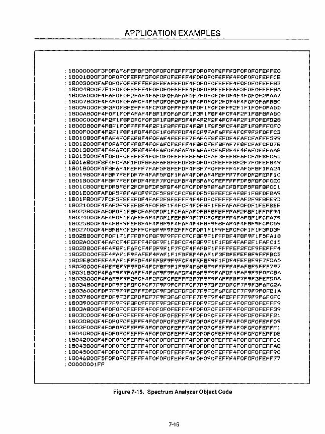
APPLICATION EXAMPLES
: 18000000F3FOF6F6FEFBF3FOFOFOFEFFF3FOFOFOFEFFF3FOFOFOFEFFEO : 18001800F3FOFOFOFEFFF3FOFOFOFEFFF4FOFOFOFEFFF4FOFOFOFEFFCE : 18003000F6FOFOFOFEFFFEFBFEF6FEFDF4FOFOFOFEFFF4FOFOFOFEFF8B : 18004800F7F1FOFOFEFFF4FOFOFOFEFFF4FOFOF8FEFFF6F3FOFOFFFF8A : 18006000F4F6FOFOF2FAF4F6FOFOFAFAF5F7FOFOFOFDF4F4FOFOF2FAA7 : 18007800F4F4FOFOFAFCF4F5FOFOFOFDF4F4FOFOF2FDF4F4FOFOF6FB8C : 18009000F3F3FOF8FEFFF4FCFOFOFFFFF4FOF1FOFOFFF2FIF1FOFOFA5D : 1800A800F4FOF1FOF4FAF4F8F1FOF6FCF1F3F1F8F4FCF4F2F1F8F8FA50 : 1800COOOF4F2F1F8FCFCFOF3F1F8F2FDF4F4F2F2F4FCF4F2F1FOFEFD28 : 1800D800F4F8F1FOFFFFF4F2F1F8FFFDF4F2F1F8F5FCF4F2F1F8FFFCFO : 1800FOOOF4F2F1F8F1FDF4FOF1FOFFFDF4FCF9FAF6FFF4FCF9F2FDFFCB : 18010800F4FAF4FOFEFBF4FOF6F4FEFFF7FAF4F8FEFDF4FAFCFAFFF599 : 18012000F4FOF6FOFFFBF4FOF6FCFEFFF4F8FCFEF8FAF7F8FCF6FCFD7E : 18013800F4F4F6FOF2FEF4F4F6FOFAFAF4F6F6FOF6FBF4F4F6FOFEFAA8 : 18015000F4FOFOFOFEFFF4FOFOFOFEFFF8F6FCFAF3FEF8F6FCFAFBFC65 : 18016800F8F4FCFAF1FDF8F6F6F8FEFDF8FOFOFOFEFFF8F2F7FOFEFB49 : 18018000F4F8F6F4FEFFF7FAF5F8FEFDF4F8F7FOFFFFF4FAF5F8FlFA24 : 18019800F4F8F7F8FDF7F4FAF5F8F1FAF4FOF6F4FEFFF7FOFDF2FEFF1C : 1801BOOOF4F8F7F8FDFDF4FEF7FOFEFBF4F8F6FCFEFFFFFDF5F8FOFCEO : 1801C800FEFDF5F8F2FCFDFDF5F8F4FCFCFDF5F8F6FCFBFDF5F8F8FCCl : 1801EOOOFAFDF5F8FAFCF9FDF5F8FCFCF8FDF5F8FEFCF4F8F1F8FDFBA9 : 1801F800F7FCF5F8FEFDF4FAF2F8FEFFF4F4FDFOFFFFF4FAF2F9F8FE9D : 18021000F4FAF2F9FEFBF4FOF8F1F4FCF4FOF8F1FEFAFAFOFOF1FEFBBE : 18022800FAFOFOF1F8FCFAFOFOF1FCFAFAFOF8F8FEFFFAF2F8F1FFFF94 : 18024000FAF4FOF1FAFEF4F4FOF1FEFBF4F2FCFCFEFFF4F6F8F1FCFA79 : 18025800F4F4F8F9FEFBF4F4F8F9F4FAF4F4F8F9F8FAF4F4F8F9FCFC59 : 18027000F4F8F8FOFEFFFCF8F9F9FEFFFCFOF1F1F9FEFCFOF1F1F3FD3F : 18028800FCFOF1F1FFFBFCF8F9F9FFFCFCF8F9F1FFFBF4F8F9F1F5FA18 : 1802AOOOF4FAFCF4FEFFF4F8F9F1FBFCF4F8F9F1FIFBF4FAF2F1FAFC15 : 1802B800F4F4F8F1F6FCF4F2F9F1F7FCF4F4FBF1FFFFFEF2FCF9FEFFF4 : 1802DOOOFEF4FAFIF9FAFEF4FAF1F1FBFEF4FAF1F3FBFEFEF8F9FFFBCE : 1802E800FEF4FAF1FFFDF4FEF8F9F9FCF4FEF8F9F1FDF4FEF8F9F7FDA5 : 18030000F4FEF8F9F9FDF4FCF8F9F1F9F4F6F8F9FFFFF4F6F8F9FFF797 : 18031800F4F6F9F9FAFFF4F6F9F9FAFDF4F6F9F9FAFDF4F6F9F9FOFC8A : 18033000F4F6F9F9F2FCF4F2FCFCFEFFFBF7F9F9FAFFFEF7F9F3FEFD5A : 18034800FEFDF9FEF8FCFCF7F9F9FCFFFCF7F9FEFEFDFCF7F9F3F6FC2A : 18036000FDF7F9F9FEFFFDFDF9F3FEFDFDF7F9F3F6FCFEF7F9F9FOFE1A : l8037800FEFDF9FBFEFDFEF7F9F3F6FCFFF7F9F9F4FEFFF7F9F9F6FCFC : 18039000FFF7F9F9F8FCFFFFF9F3FEFDFFFDF9F3F6FCF4FOFOFOFEFFF9 : 1803A800F4FOFOFOFEFFF4FOFOFOFEFFF4FOFOFOFEFFF4FOFOFOFEFF39 : 1803COOOF4FOFOFOFEFFF4FOFOFOFEFFF4FOFOFOFEFFF4FOFOFOFEFF21 : 1803D800F4FOFOFOFEFFF4FOFOFOFEFFF4FOFOFOFEFFF4FOFOFOFEFF09 : 1803FOOOF4FOFOFOFEFFF4FOFOFOFEFFF4FOFOFOFEFFF4FOFOFOFEFFFI : 18040800F4FOFOFOFEFFF4FOFOFOFEFFF4FOFOFOFEFFF4FOFOFOFEFFD8 : 18042000F4FOFOFOFEFFF4FOFOFOFEFFF4FOFOFOFEFFF4FOFOFOFEFFCO : 18043800F4FOFOFOFEFFF4FOFOFOFEFFF4FOFOFOFEFFF4FOFOFOFEFFA8 : 18045000F4FOFOFOFEFFF4FOFOFOFEFFF4FOFOFOFEFFF4FOFOFOFEFF90 : 18046800F5FOFOFOFEFFF4FOFOFOFEFFF4FOFOFOFEFFF4FOFOFOFEFF77 :00000001FF
Figure 7-15. Spectrum Analyzer Object Code
7-16

Design Considerations 8

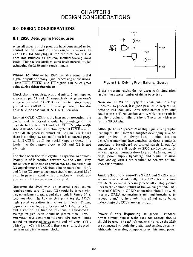
CHAPTER8 DESIGN CONSIDERATIONS
8.0 DESIGN CONSIDERATIONS
8.1 2920 Debugging Procedures
After all aspects of the program have been tested under control of the Simulator, the designer programs the 2920 EPROM and plugs it into the breadboard. If it does not function as desired, troubleshooting must begin. This section outlines some basic procedures for debugging the 2920 and its environment.
Where To Start-The 2920 includes some useful digital outputs for many signal processing applications. These EOP, CCLK, and OF signals can be of great value during debugging phases.
Check that the required plus and minus 5 volt supplies appear at pin 18 and 12. respectively. A scope won't necessarily reveal if GRDD is connected, since scope ground and GRDD are the same potential. This also holds true for VSP and RUN. Check them also.
Look at CCLK. CCLK is the instruction execution rate clock, and its period should be one-sixteenth the crystal/clock rate at Xl and X2. CCLK's pulse width should be about one instruction cycle. If CCLK is at or near GRDD potential almost all the time, check that there is a pullup resistor (and that it is connected properly). If CCLK is still not working appropriately, it is likely that the master clock at Xl and X2 is not adequate.
For clock operation with crystal, a capacitor of approximately 15 pf is required between X2 and VBB. Stray capacitances must also be considered, i.e., the sum of all X2 capacitances to VBB should be no more than 15 pf, and X 1 to X2 stray capacitance should not exceed 15 pf also. In general, good wiring practices will avoid any problems with the operation of a crystal.
Operating the 2920 with an external clock source requires some care. X 1 and X2 should be driven with true-complement signals, and the circuit in Figure 8-1 is recommended. The key starting point for the 2920's high speed operation is the master clock. Timing requirements include a duty cycle of 50±5 0/0, or better, and a rise or fall time of less than 5 nanoseconds. Voltage "high" levels should be greater than -1 volt, and "low" levels less than -4 volts. Rise and fall times should be measured between -1 and -4 volts. (TTL with V cc = -·5 V .) If CCLK is jittery or erratic, the problem is usually in the master clock.
8-1
INPUT 010 -5 VOLTS
GRDD
-5V 47011
D--4~ ____ --,1""15 XTAL1
GRDD
-5V
47011
,--_~~_....:.1=i6 XTAL2
Figure 8-1. Driving From External Source
If the program results do not agree with simulation results, there are a number of things to review.
Noise on the VREF supply will contribute to many problems. In general, it is good practice to keep VREF noise to less than 4mv. Any noise greater than 4mv could cause AID conversion errors, which can result in stability problems in digital filters. The same holds true for the GRDA pin.
Although the 2920 processes analog signals using digital techniques, the hardware designer developing a 2920-based product must always keep in mind that the device's primary interface is analog. In effect, standards applying to breadboard or printed circuit layout for analog circuitry still apply to 2920 environments. In general, special consideration to ground planes, guard rings, power supply bypassing, and digital isolation from analog signals are required to achieve optimal 2920 performance.
Analog Ground Plane-The GRDA and GRDD leads are not connected internally in the 2920. A connection outside the device is necessary to tie all analog ground lines to the common return of the system ground. That external GRDA to GRDD connection should be such that the GRDA connection is minimal impedance (a ground plane) to help minimize digital noise being induced into the 2920's analog section.
Power Supply Bypassing- In general, standard power supply bypass techniques for analog circuits should be used. The ±5 volt power pins inside the 2920 are connected to both the digital and analog circuitry. Although the analog components exhibit good power
DESIGN CONSIDERATIONS
supply rejection, it is considered good practice to provide bypass capacitors for both high and low frequency components. The pins RUN, VSP, M1, M2 should be considered power supplies for layout considerations.
Noise And Layout Considerations-The 2920 pin configuration allows easy isolation of digital and analog signals in a PC board environment. The digital and analog signal lines should be on different sides of the PC board, and all analog signals to and from the 2920 are separated by the analog ground runs. This provides a stable (GRDA) level to minimize signal coupling, in effect, a shield. The two leads of the sample and hold capacitor should be "shielded" from each other by GRDA also, at both sides of the capacitor.
If the 2920 is to be used with an IC socket, pin-to-pin crosstalk must be minimized. Some popular IC sockets can exhibit as much as 40mv of crosstalk, with full scale signals which could seriously affect the integrity of the 2920's AID and 01 A conversions.
8.2 Description Of Application Breadboard
The 2920 Application Breadboard was designed for general purpose applications while maintaining a low noise system. The board is easy to assemble since it requires only a handful of components. The following description of the application breadboard may be enhanced by referring to the pin out description (Figure 8-2 and Table 8-1) and the schematic diagram (Figure 8-3).
For proper operation of the 2920, the required inputs are +5 volts, -5 volts, and a clock. The board provides lowpass filters at the power supply inputs and bypass. capacitors at the voltage pins so that high frequency signals and voltage spikes will not enter into the chip. There are four multiplexed analog inputs and eight multiplexed analog outputs provided on the board. Pin 7 and 9 have a 500 pF sample and hold ceramic capacitor connected between them.
VREF (Pin 8) is the reference voltage needed for the AID-OJ A conversion. This voltage is provided by the output of a voltage following amplifier. It is important for proper A/D-DI A conversion that VREF remain constant and provide a noise free voltage source. To ensure a low noise DC output a shunt capacitor is located at the input of the op amp. Also a bypass
8-2
capacitor is connected between VREF and GRDA. The noise at the VREF pin should not exceed 4 m V. If it exceeds 4 m V, the noise will couple into the A/D-DI A converter and appear as noise on the signal. The input and output voltage range is ± VREF, and VREF can be adjusted between plus one and two volts via a potentiometer.
Pull up resistors and test points are located at OF (Pin 22), RST/EOP (Pin 21), and CCLK (Pin 19) to enable the user to observe the timing and overflow status of the 2920 while it is operating.
Since the 2920 is a sampled data system, it is necessary to band limit the input signals, SIGIN(K), to about V3 the sampling rate. If the signals are inherently band limited (e.g., sine waves), no filters are needed, otherwise the user must provide lowpass filters to band limit the signals before entering the 2920 signal processor.
8.2.1 Layout Considerations
Some guidelines are offered in this section which were taken into consideration when designing the 2920 application breadboard. For the prototype board built at the Intel factory, a custom general purpose breadboard was used; however commercially available breadboards may also be used. In the parts list there is a recommendation for a commercially available breadboard. If a general purpose breadboard is used, the noise can be reduced by employing thick gauge bus wire for the power supplies and the grounds. The layout guidelines listed below will aid in realizing a low noisellow crosstalk circuit.
a) Bypass the +5V and -5V power supply voltage with a 100 IlF capacitor and a .1 IlF ceramic capacitor with a 1-3 Q resistor in series. This will reduce high frequency signals and voltage spikes from entering into the board from the power supplies. Make sure the voltage drop across the series resistance does not reduce the voltage at the 2920 power supply pins below specification.
b) Separate digital signals from analog signals where possible to ensure a minimal amount of cross-coupling.
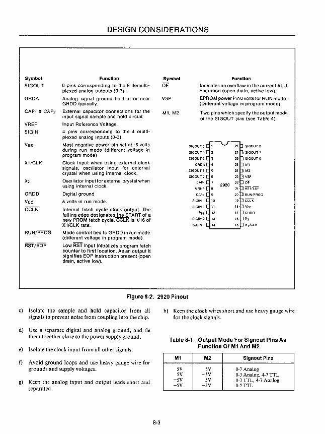
DESIGN CONSIDERATIONS
Symbol Function
SIGOUT 8 pins corresponding to the 8 demulti-plexed analog outputs (0-7).
GRDA Analog signal ground held at or near GRDD typically.
CAP, & CAP2 External capacitor connections for the Input signal sample and hold circuit
VREF Input Reference Voltage.
SIGIN 4 pins corresponding to the 4 multi-plexed analog Inputs (0-3).
Vss Most negative power pin set at -5 volts during run mode (different voltage in program mode)
X1/CLK Clock input when using external clock signals, OSCillator input for external crystal when using internal clock.
X2 OSCillator input for external crystal when using internal clock.
GRDD Digital ground
Vee 5 volts in run mode.
CCLK Internal fetch cycle clock output. The falling edge designates the START of a new PROM fetch cycle. CCLK is 1/16 of X1/CLK rate.
RUN/PROG Mode control tied to GRDD in run mode (different voltage in program mode).
RST/EOP Low RST input initializes program fetch counter to first location. As an output it signifies EOP instruction present (open drain, active low).
Symbol
OF
VSP
M1, M2
Function
Indicates an overflow in the current ALU operation (open drain, active low).
EPROM powerPrnOvoltsforRUN mode. (Different voltage in program mode).
Two pins which specify the output mode of the SIGOUT pins (see Table 4).
SIGOUT 3 SIGOUT 2
SIGOUT 4 SIGOUT 1
SIGOUT 5 SIGOUT 0
GRDA Ml
SIGOUT 6 M2
SIGOUT 7 VSP
CAP! OJ!
VREF RST/EOP
CAP2 RUN/PROG
SIGINO CClK
SIGIN 3 Vee
Vee GRDO
SIGIN 2 X2
SIGIN 1 XI/ClK
Figure 8-2. 2920 Pinout
c) Isolate the sample and hold capacitor from all signals to prevent noise from coupling into the chip.
d) Use a separate digital and analog ground, and tie them together close to the power supply ground.
e) Isolate the clock input from all other signals.
f) Avoid ground loops and use heavy gauge wire for grounds and supply voltages.
g) Keep the analog input and output leads short and separated.
8-3
h) Keep the clock wires short and use heavy gauge wire for the clock signals.
Table 8-1. Output Mode For Signout Pins As Function Of M1 And M2
M1 M2 Signout Pins
5V 5V 0-7 Analog 5V -5V 0-3 Analog, 4-7 TTL
-5V 5V 0-3 TTL, 4-7 Analog -5V -5V 0-7 TTL

Vee
DESIGN CONSIDERATIONS
Vee = +5V
VBB = -5V
SIGOUT 7 SIGOUT 5 SIGOUT 3
SIGOUT 6 SIGOUT 4
SIGIN 3
SIGIN 0
SIGOUT 2 SIGOUT 0
SIGOUT 1
-5V +5V
Figure 8·3. Schematic Diagram 2920 Application Breadboard
8-4
DESIGN CONSIDERATIONS
8.2.2 Parts List
ICI 2920 Signal Processor IC2 LM308AH Operational Amplifier IC3 74S04 Hex Inverter IC4 LM336 Reference Diode
13 BNC Connectors 1 28 Pin Socket
PI 5KQ Potentiometer
Rl R2 R3 R4 R5 R6 R7 R8 R9 RIO Rll R12 R13
I.OKQ 1.5KQ 3.9KQ 100KQ 62Q IOKQ IOKQ IOKQ IOQ IOQ IOQ 10Q IOQ
Resistor (Note 1) Resistor (N ote 1) Resistor (Note 1) Resistor (Note 1) Resistor (Note 1) Resistor (Note 1) Resistor (Note 1) Resistor (Note 1) Resistor (Note 1) Resistor (Note 1) Resistor (Note 1) Resistor (Note 1) Resistor (Note 1)
8-5
C 1 1.0 J.LF Ceramic Capacitor C2 1 J.LF Ceramic Capacitor C3 500 pF Ceramic Capacitor C4 1 J.LF Ceramic Capacitor C5 100 J.LF Tantalum Capacitor C6 .1 J.LF Ceramic Capacitor C7 .1 J.LF Ceramic Capacitor C8 100 J.LF Tantalum Capacitor C9 1 J.LF Ceramic Capacitor CIO 1 J.LF Ceramic Capacitor CI1 .1 J.LF Ceramic Capacitor
(Note 2) (Note 2) (Note 2) (Note 2) (Note 2) (Note 2) (Note 2) (Note 2) (Note 2) (Note 2) (Note 2)
Breadboard custom made for (Notes 3 and 4) Intel
NOTE:
1) All Resistors 1f4 watt, carbon composite, ± 100/0. 2) All Capacitors are non-polarized. 3) IC Breadboard substitute: Douglas Electronics,
Inc. Part No. 22-DE-6 4) The breadboard should use 16-22 gauge bus
wire for voltages and grounds (see layout considerations).


2920 Support Tools 9
,
\
:E w Ien >en Iz w :E a.. o ...J W > W c a: o en en w (.) o a: a..
CHAPTER 9 2920 SUPPORT TOOLS
9.0 2920 SUPPORT TOOLS
The 2920 Signal Processing Software Support Package (SPS-20) consists of the three powerful tools a designer needs in order to create signal processing products based on the 2920: the 2920 Signal Processing Applications Software/Compiler, the 2920 Assembler, and the 2920 Simulator. These tools facilitate the implementation, verification and debugging of 2920 programs.
9.1 The Assembler
The 2920 Assembler translates assembly language mnemonics programs into the machine code of the 2920 chip. The designer, usually working from a block diagram, creates 2920 assembly code routines for each functional block.
These routines are typed in to a diskette file, using the Editor under the Intel Systems Implementation Supervisor (ISIS-II) provided as part of the Intellec Development System. Revisions to any part of the program or commentary text entered are easily made using this Editor.
After the program has been developed and edited into a form ready to test, the Assembler can be invoked.
The assembler translates 2920 mnemonics (such as ADD or L02 or IN3) into machine code. At the same time, it produces an object file and a listing showing each source line and the generated code, plus any detected errors. Its object output may be used by the EPROM programmer and the 2920 Simulator.
You can control the operations of the assembler with respect to most of its functions. This control may be exercised in the command invoking the assembler, or in control lines embedded in the source program.
The individual functions of this assembler are: 1) Symbol Table Management: keeping track of all
symbols and their values and automatically assigning RAM locations to variable names as they are encountered.
2) Location Counter Management: keeping track of locations available for instructions and assigning locations for each instruction assembled.
9-1
3) Instruction Assembly: translating mnemonic opcodes and operands into their machine language equivalents.
4) Control and Directive Processing: noting and executing all controls, e.g., assembly listing and object output control, and directives such as symbol definition. This includes controls given as part of the invocation command.
5) Assembler Output Generation: creating the assembly listing, object code file, and error diagnostics.
A sample 2920 assembly listing is shown in Figure 9-1.
9.2 The Simulator
The SM2920 Simulator is the software module which simulates operations of the 2920 device under control of the program to be stored in the EPROM.
The SM2920 software eases the testing and modification of 2920 programs. It does so by
• facilitating the use of symbolic references for displaying or changing all 2920 registers, flags, and user-named locations in program or data memory
• tracing, during simulation, the values of user-selected items chosen before starting simulation, enabling the programmer to see when and how signals are sampled and handled by a program
In general, the SM2920 module allows the user to • load object programs from ISIS disk files • define input signals as functions of time and pro
cessor variables or states • establish halting conditions for each simulation • create, display, and modify variable values and
instructions • simulate a program, including sampling the input
signals as defined above, either one step at a time or in sequence, from zero or other user-specified addresses save tested or modified code into ISIS disk files
9.2.1 Concepts of Simulation, Testing, and Debugging
After writing and assembling a 2920 program, there is a need to determine the performance of the implementation. Inputs must be specified, one or more instructions

2920 SU PPORT TOOLS
ISIS-II 2920 ASSEftBLER XI02 PACE
AS~EftBLER INYOKED BYI AS2'20 SAW ASft DEBUG
SAWTOOTH WAVE GENERATOR
LIHE LOC OBJECT SOURCE STATEftENT
$T I TLE(' SAWTOOTH WAYE GENERATOR' )
4 OOOOEF 's OOOOEF Ii OOOOEF
:3 008REB S 4 008ROA C) 5 OOHEF
~O 6 7A8AED ,1 7 6000EF !2 8 7082EF ; 3 , 4044EF :4 10 4000EF :5 11 4000EF 16 12 4000EF ~ 7 13 8000EF !8 14 8000EF ,':I 15 8000EF 20 16 SOOOEF 21 17 8000EF 12 18 8000EF 23 l' SOOOEF 24 ';:5
SYI'IBOL:
RS~E~BLY COI'IPLETE ERROPS 0 WARHIHGS 0 RAI'IS!ZE 1 RO~S!ZE 20
INO INO IHO SUB Y,KP1,IHO SUB '(,KPLRLIHO LOA DAR,Y.IHO ADD '(,KP7,CHDS CYTS LDA Y,KPO,CHDS LOA DAR,'( HOP HOP HOP OUTO OUTO OUTO EOP OUTO OUTO OUTO
EHO
YALUE:
SAftPLE INPUT CHANHEL 0
SII'IULTAHEOUSLV CALCULATE SAWTOOTH BY SUBTRACTIHC 3/1' FRO" Y ALSO CHECK SIGH BIT OF V IF Y HEGATIYE START HEXT TOOTH COHYERT SA"PLED IHPUT TO DICITAL (SIGH BIT) SUPPRESS SAWTOOTH IF IHPUT WAS < 0 PREPARE TO OUTPUT SAWTOOTH AHALOC LEYEl I'IUST SETTLE
OUTPUT SAWTOOTH
PROGRA" WILL EHD IH THREE "ORE IHSTRUCTIOHS
Figure 9-1. Sample 2920 Assembly Listing
simulated, and execution halted at a preselected location or condition, in order to review how the simulation is progressing. This controlled break in execution is called a BREAKPOINT.
The ability to review the values of key variables or the steps of the simulation, as they occurred prior to the breakpoint, is called tracing, i.e., collecting and displaying TRACE information. Similarly, it is useful to be able to display and alter data or instructions in any Random-Access-Memory (RAM) or Read-OnlyMemory (simulated EPROM) locations, respectively. RAM is data memory and EPROM is program memory.
The 2920 Simulator provides all of the above capabilities. The use of symbolic names instead of numeric addresses further facilitates the process of program checkout by permitting the use, in debugging, of
9-2
the same names as were used in defining the problem and setting up the original assembler code.
9.2.2 Modes of Operation
The Simulator operates in two modes: Interrogation Mode and Simulation Mode. Interrogation Mode occurs whenever the Simulator is not actually simulating a program. This mode can be used to prepare the system for a new operation or to investigate the results of the last operation.
The 2920 program residing in memory is simulated during Simulation Mode. Trace data are collected and displayed during simulation. Breakpoints set under Interrogation Mode can include a number of different combinations of conditions. When these conditions are
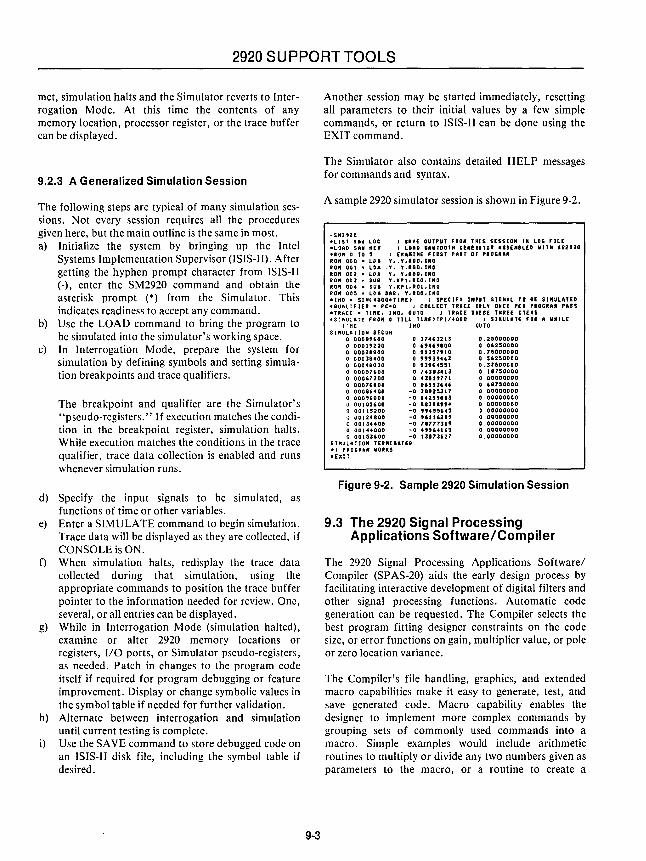
2920 SUPPORT TOOLS
met, simulation halts and the Simulator reverts to Interrogation Mode. At this time the contents of any memory location, processor register, or the trace buffer can be displayed.
9.2.3 A Generalized Simulation Session
The following steps are typical of many simulation sessions. Not every session requires all the procedures given here, but the main outline is the same in most. a) Initialize the system by bringing up the Intel
Systems Implementation Supervisor (ISIS-II). After getting the hyphen prompt character from ISIS-II (-), enter the SM2920 command and obtain the asterisk prompt (*) from the Simulator. This indicates readiness to accept any command.
b) Use the LOAD command to bring the program to be simulated into the simulator's working space.
c) In Interrogation Mode, prepare the system for simulation by defining symbols and setting simulation breakpoints and trace qualifiers.
The breakpoint and qualifier are the Simulator's "pseudo-registers." If execution matches the condition in the breakpoint register, simulation halts. While execution matches the conditions in the trace qualifier, trace data collection is enabled and runs whenever simulation runs.
d) Specify the input signals to be simulated, as functions of time or other variables.
e) Enter a SIMULATE command to begin simulation. Trace data will be displayed as they are collected, if CONSOLE is ON.
f) When simulation halts, redisplay the trace data collected during that simulation, using the appropriate commands to position the trace buffer pointer to the information needed for review. One, several, or all entries can be displayed.
g) While in Interrogation Mode (simulation halted), examine or alter 2920 memory locations or registers, 110 ports, or Simulator pseudo-registers, as needed. Patch in changes to the program code itself if required for program debugging or feature improvement. Display or change symbolic values in the symbol table if needed for further validation.
h) Alternate between interrogation and simulation until current testing is complete.
i) Use the SAVE command to store debugged code on an ISIS-II disk file, including the symbol table if desired.
9-3
Another session may be started immediately, resetting all parameters to their initial values by a few simple commands, or return to ISIS-II can be done using the EXIT command.
The Simulator also contains detailed HELP messages for commands and syntax.
A sample 2920 simulator session is shown in Figure 9-2.
-5112'20 'L1ST SAW LOC I SA¥[ OUTPUT FlU THIS SESSION IN LOC FILE 'LOAD SAW NEX I LOAO UIITOOTH '[NEUTOI ASSEII8LEO IIITN ASU20 'ROII 0 TO 5 I EKAIIINE FIRST PUT OF PIDCIAft ROil 000 - LOA Y •. Y .100.1110 ROil 001 - LOA .Y. Y.IOO.1II0 ROil 002 - LOA Y. Y.IOO.IIIO ROil 003 - SUB Y.lPI.IOO.lNO ROil 004 - SUB Y.lPI.ROI.lNO ROil 005 - LOA OAR. Y.ROO.lNO 'IHO • SIN(40000TlIIE) I SPECIFY IN'UT SIeNAL TO BE snULATEO .QUALIFIER - Pc-o I COLLECT TRACE ONLY ONCE PER PROCR,," PASS 'UACE - TIllE. INO. OUTO I TRACE THESE THREE ITEIIS 'S:/IULATE FROII 0 TILL TlIIE>TPl/4000 I snULATE FOR A WHILE
T'ME IHO OUTO SIIIULATION BEeUN
o 0000"00 0 J7U3213 o OOOU200 0 "."800 o 00021800 0 U3S7UO o 00038400 0 "U'U3 o 00048000 0 93".S51 o ooosaoo 0 74303413 o 000'7200 0 Ulun1 o 0007"00 0 O"SUH o 000U400 -0 3092S317 o 000"000 -0 '42"883 .J 00105'00 -0 B830.,,. o 00115200 -0 "4SSU5 .J 00124800 -0 'UU2U o 00134400 -0 717773U o 00144000 -0 4"'41" o 00153'00 -0 13I7U27
SIIIULATION TEIIlIKATEO ., PROCIAII WORKS oEXI T
0.25000000 o onsoooo 0.7S000000 o SUSOOOO o .37S00000 o 18750000 o 00000000 o "750000 o 00000000 o 00000000 o 00000000 o 00000000 o 00000000 0.00000000 o 00000000 0.00000000
Figure 9-2. Sample 2920 Simulation Session
9.3 The 2920 Signal Processing Applications Software/Compiler
The 2920 Signal Processing Applications Software/ Compiler (SP AS-20) aids the early design process by facilitating interactive development of digital filters and other signal processing functions. Automatic code generation can be requested. The Compiler selects the best program fitting designer constraints on the code size, or error functions on gain, multiplier value, or pole or zero location variance.
The Compiler's file handling, graphics, and extended macro capabilities make it easy to generate, test, and save generated code. Macro capability enables the designer to implement more complex commands by grouping sets of commonly used commands into a macro. Simple examples would include arithmetic routines to mUltiply or divide any two numbers given as parameters to the macro, or a routine to create a
2920 SUPPORT TOOLS
sawtooth oscillator of varying slope. When such code is needed, it can be generated with one call to the macro along with the appropriate parameters.
The Compiler makes it easy to specify signal processing functions in a modular manner and to join the resulting code modules 'into larger programs. One important application is the development of digital filters, and the SP AS20 Compiler contains a number of features relevant to their design.
The Compiler operates interactively, permitting the designer to
• set sampling rate, place poles and zeros at chosen S-plane or Z-plane coordinates, and set error bounds on gain
• see immediately, on a graph or list, the frequency or time response of existing poles and zeros at specified frequencies, or display any design parameter
• generate, store, and review 2920 assembly language code for each filter or stage, or other signal processing functions
• use diskette files as scratchpads to store, review, modify, and retrieve files of parameters, code, or commentary
• create sequences of commands pertinent to complex or frequently used functions as macros, naming and storing them on diskette files for ease of future use, facilitating later interactive design sessions or unattended test sessions.
The Signal Processing Applications Software/Compiler accepts high-level language input and produces 2920 assembly language, as described above. The Compiler is also a filter design aid which permits substantial interactive manipulation of a wide variety of parameters and constraints, both in design of digital filter stages and in optimization of the 2920 code in terms of size and error limits. One principal feature allows specification of the poles and zeros of a desired filter and, after designer review of the pertinent graphs, the automatic implementation of that filter in 2920 assembly code, without having to write each of the detailed steps that are required in assembly language.
Concepts of Filter Design-Designing a filter involves choosing operations to perform on signals in order to produce modified signals. These operations are
9-4
usually (but not always) linear. The theory relating continuous analog filters to sampled digital filters appears in Chapter 5.
Filters are usually designed to achieve certain gain anc;l phase characteristics, which can be viewed as resulting from the location of the filter's poles and zeros. The desired output amplitude and phase can be approached in an interactive design session by placing poles and zeros in the S-plane (for continuous fitlers) or the Z-plane (for sampled filters), and viewing the resultant output. Moving these poles and zeros can then change that output to more closely approximate what is needed. The Compiler capabilities facilitate this interactive process of specification, modification, and review by providing simple commands and graphs for these functions.
Displaying Responses-Frequency and time responses of the filter can be examined as the positions of poles and zeros are manipulated. The gain, phase, group delay, and step or impulse responses can be graphed or listed. The frequency range of interest for these outputs can be specified. While emphasis is placed on the gain versus frequency response of the filter, designers can take advantage of the compound command capability to use the phase, impulse, or step responses.
The graphs do not require the console device to have any cursor controls, e.g., the ability to move the beam directly by pressing a buttom for up, down, left, or right. The user specifies the X-axis and the Y-axis ranges. The last curve plotted is always available for redisplay upon entering the command GRAPH, regardless of the effect of intervening commands. It is also possible to superimpose the last curve plotted and a new curve, regardless of intervening scale changes. The graphs can be sent to a diskette file, or hard copies can be produced on a line printer, since no special cursor control charcters are assumed.
Generating Code-Once the filter characteristics (e.g., gain, error, phase) look adequate to meet the design specifications, the user can generate the code for each pole or zero with a single command. The Compiler enables implementation of the filter as cascaded series of first and second order stages. It also supports the generation of code to compute independent variables of the form Y=C*X or Y=C*Y, where C is a constant, and
2920 SUPPORT TOOLS
X and Yare variable names. These equations are useful for propagation and scaling of the digital signal between stages.
These modules of assembly language code, for each pole or zero, can be accumulated into a file to be used as input to the 2920 Assembler. During code generation for one stage of a filter, it may be desirable to sacrifice a certain amount of numerical accuracy in order to get a shorter program. Towards this end, code generation, is performed subject to constraints which the user can specify. One such constraint consists of piecewise linear bounds on the gain, in decibels, as a function of frequency. The Compiler then strives to minimize the mean-square deviation from these bounds.
Before saving the resulting code into a file, designers can interactively adjust the number of instructions or the error constraint in order to achieve the shortest program with a tolerable error. This new code can then be saved into a file.
Filing And Retrieving Code Or Parameters-The process described above, of specification, display, and adjustment, is extremely interactive. The file commands have been structured to facilitate the restart of an inter-
-:F1 SPAC20 SFT
rupted design or test session. They also make it easy to accumulate, into one or many files, the partial results of specifying parameters or creating code. Parameter files saved from an interrupted design session can then be included at a later date, to resume that design session with all relevant variables restored to their condition at the time the session was interrupted.
Compound Commands-SP AS20 contains macro and compound command facilities which enable multiple and conditional execution of command sequences, including substitution of varying parameters. These capabilities enable users to extend the language itself by defining their own commands and constructs.
Such macros make it possible, for example, to define an iterative process of moving poles and zeros and graphing the resultant response without having to type all the commands during each iteration of that process. Conditional code generation and display could be included in such a procedure. Macros and compound commands are interruptable at any time via the console ESCape key, should error or time constraints make that desirable.
A sample SPAS20 session is shown in Figure 9-3.
ISIS-II 2HO SICNAL PROCESSING APPLICATIONS conPlLER. VI 0 o oDEFINE POLE I • -707.707 , CREATE A POLE IN CONTINUOUS S-PLANE o oP: • LIST ALL POLES AND ZEROS POLE I • -707 00000.707 OOOOO.COHT IHUOUS o orSCALE • 100.10000 , EsaBL ISHES FREQUEHC\ RANCE OF INTEREST . OY$C~LE • -4~.1 , ESTABLISHES nACHI TUDE HSPOHSE RANCE OF INTEREST . oCR';PH CAIN , PLOT ftACNITUDE RESPONSE OF POLE PAIR
CA IN I 0 --------------------------
-:< ~
-~ " ... ., ~
"':0 I)
-Il I -H ; -I ~ 5 -13 --20 ~
-ll I - 2~ :< -2" '5 -z~ .,. -] I , -H J - Jo; l -33 4 ... 41j to
... <4? ~
... 45 ., DB I HZ I
100 I~O 200 JOO 400 500 700 1000 1400 2000 3000 5000 10000
Figure 9-3. Sample SPAS20 Session
9-5
2920 SU PPORT TOOLS
THE UNITS USED IN CRAPHIN~ CAIN ARE SHOWN IN THE LOWER LEFT CORNER GAIN IN HCIBElS IS CRAPHED YERSES FREQUENCY IN HERTZ
PPEPUE TO MYE TO TNE DICITAL DOftAIN o $AftPlE RATE RUST BE SPECIFIED o or> • In3020 J RATE FOR 192 INSTRUCTION PROCPA" AND 10ftHZ CLOCK TS • 7 n0500./10 .. '
O"')~'E POLE TO Z I CONYERT FILTER TO DICITAL Ylr. "ATCNED-Z TRANSFORIIATIOH I rOLESIZHOES "DYED
Op , LIST TRANsrORIIED POLE PO~E I • 0 71092B36.0 341183".2
o CO"PARE RESPOHSES OF THE ANALOC ANO DICITAL FILTERS BY CRAPHINC THE 0' HEW RESPONSE OYER THE OLD
-: i. -1 • ... 1) •
-- ~ -I') 0 -12 I -1" , ... ! i -lO -ll ' -l~ -]- , - 2' --3. :. -'4 .:, ... 3 ~ " -H • -'J, -41 ~ -4~ )
('6 I H2 ' 100 150 200 300 400 500 700 1000 1400 2000 3000
c·
F'LUS SICHS INDICATE OLD CURVE HOTE THAT THE DICITH FILTER RESPOHSE BEGINS TO IHCREASE ACAIN AT HAlF THE SAIIPlE RIITE ( "10 NZ )
THE PHASE CHARACTHISTICS OF THIS FILTER CAM BE EXA"IHED . • ','StolLE • -Fl.PI . • CR"PH PHASE
PH':'S£ 3 :. 2 H 2 ~ 4 2 24 I ,.
I '5 135 I 05 o 75 a • 5 o ! 5
I ESTABLISHES RANCE OF INTEREST
-0 15 ...... ---------0 '5 -0 ~5
-I O~
-I 35
-I " -I ,.
-2 2' -2 5' -2 8. -3 14
RAD I HZ I
100 150 200 300 400 500 700 1000 14('0 2000 3000 p.
5000
5000
'~~T .FI POLE P2 I SAVE THE POLE lOCAT ION lH A DISK FILE BAUUP
.. .
.!.·'l't, Pi'LE 1 IH~l(ll : ~lr~t~ ... ,t. ,';t.L! r..:~l"tL) l.llC'( FI,.,j;' IHI~ tILIt." B.=I 3HB"'0 B2--0 '05.191.
Figure 9-3. Sample SPAS20 Session (Cont'd.)
9-6
10000
10000
2920 SUPPORT TOOLS
, OrTI"IZED 2'20 CODE IS NOW CENERATED TO SAVE SrACE. SOliE .)F THE SCREE" OUTPUT HAS BEEH DElETED HORftALLY ALL ATTEftPTS BY THE COIIPILER TO CEHERATE CODE ARE ECHOED ON THE SCREEN I
IHiT-IO P(lLE I - 0 710U458.0 3411677'.2
BEST' PERROR - J Jn~874110"5" 5884'H7110 __ '
: NOTE' IIAkE SURE SICNAl 15 <0 7463'571 LO~ ~UTZ_PI.OUTI_PI.ROO
, OUT2_PI-I OOOOOOOO-OUT!_PI LOA OUTI_PI. OUTO_PI.ROO
• OUTI_PI-I OOOOOOOO-OUTO_PI SUB au TO_PI. OUll_PI .R05
• OUTO_PI-I OOOOOOOO-OUTO_PI-O OJI250000-0Ull_PI ADO OUTO_PI.OUTO_PI.ROJ
· OUTO_P I-I 12500000-0UTO_P 1-0 OJ5156Z50-0UTI_' I ADD OUTO_PI.OUTI_PI.R02
: OUTO_PI-I 12500000-0UTO_'1+0 2148417'-OUTI_FI SUB OUTO_PI.OUT2_PI.ROI
• OUTO_PI-t 12500000_0UTO_PI+0 21484175_0UTI_PI-0 50000000-0UTZ-PI SUB OUTO_PI. OUTLPI .ROB
• OllTO_PI-1 12500000_0UTO_PI+0 214B4175_0UTI_PI-0 50B0625-0UT2_PI ADD OUTO_PI. OUTZ_PI.RlI
• OUTO_PI-I IZ50000000UTO_PI+0 2148437'_OUTI_PI-0 '03417HoOUTZ_PI SUB OUTO_Pl. OUT2_PI .RO'
, OUTO_PI-I IZ500000_0UTO_'I+O 214B4175-0UTLPI-0 5051710'.OUTZ_PI ADO OUTO_Pl.IHO_PI.ROO
-
: OUTO_PI-I 12500000-0UTO_'1+0 214B4375-0UTI_PI-0 'O'1710'-OUT2_PI-1 OOOOOoOOoINO.PI
THE CODE COIIIIANO SPECIFIH THAT THE POLE PAIR BE CODED IN LESS THAN II INSTRUCTIONS. SO 10 INSTRUCTIOHS VERE CENERATED. WITH COllRENTS THE FINAL ERROR 1M RADIUS AHD ANGLE FOR THE POLE PAIR WAS OF THE ORDER OF 1110'" AS INDICATED A80YE IH PHROR THIS OPTIIIIZ[O H20 ASSEIIBLY CODE CAN HOW BE APPENDED TO A FILE WHICH IIAY CONTAI" OTHER COOED FUHCTlONAL BLOCKS or A H20 PROCRAII
-r (I T
Figure 9-3. Sample SPAS20 Session (Cont'd.)
9-7


Appendix-Evaluating 2920 Applications


r
r
\..
r
\..
EVALUATING 2920
APPLICATIONS
POTENTIAL APPLICATIONS CAN BE
DIVIDED INTO THREE CATEGORIES
Those which the 2920 can definitely do.
Those which It definitely cannot do. (50kHz BW, or 90dB Dynamic Range)
Those which fall Into a gray area.
QUESTIONS TO ASK YOURSELF WHEN
APPENDIX
""
For many applications, the 2920 can either definitely be used, or definitely not be used. However, sometimes it is not clear whether a potential application can be done by the 2920. Some examples which fall into this gray area are those applications where complexity/bandwidth constraints can't quite be met, but it might be possible to sacrifice on one constraint to meet the other. Or those applications where a very detailed analYSis would have to be made, and a prototype program actually written to determine applicability of the 2920. In many cases where an entire application, as specified by the customer, cannot be done with one 2920, part of it could be done, reducing costs and component count sufficiently to give the 2920 an advantage over another solution.
EVALUATING A POSSIBLE 2920 APPLICATION
Is 2920 dynamic range adequate? The dynamic range with be 6dB/Blt for a total of 54dB with a 9-blt conversion.
Does the bandwidth needed by the application under consld· eratlon fall within the range the 2920 can handle?
Nominally 0-10 kHz, and up to about 15kHz.
Will the program length which Is required to obtain the desired bandwidth allow for the Implementation of the desired function or functions?
Will 40 RAM locations be enough?
Can the 2920 handle the I/O requirements with Its 4 Input and 8 output channels?
.,J
A-1

APPENDIX
r DYNAMIC RANGE
• Dynamic range Is defined as the ratio 01 the peak signal to the smallest detectable signal.
• Determined by the number 01 bits 01 the AID conversion.
• A 9·blt AID corresponds to a 54dB dynamic range.
- So, lor a threshold detection with the 2920, lor example, there will be a 54dB dynamic range (max.)
- However, " an application requires a minimum SNRa for processing, then the total signal range will be:
54dB- SNRa
where SNRa Is the minimum signal to quantization noise ratio that Is acceptable.
QUANTIZATION NOISE
M~ _______ ...,.:..... ______ _
OUTPUT VOLTAGE
Jo = 2N-l
N = #BITS
Jo ~ 6N DB
IMAX
I I I I
1 : ERROR VOLTAGE I
t\. t\. I\. t\. t\ I\. I
INPUT VOLTAGE
INPUT VOLTAGE
A-2
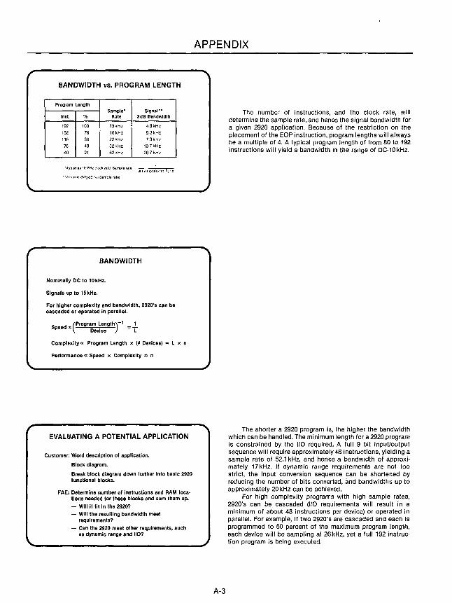
BANDWIDTH vs" PROGRAM LENGTH
Program Length Sample" Signal""
Inst. % Rate 3dB Bandwidth
192 100 13kHz 43kHz
152 79 16kHz 53kHz
116 60 22kHz 73kHz
76 40 32kHz 107kHz
40 21 62kHz 207kHz
·Assumes 10MHz clock rate Sample rate = (;' Ins! )(4~ x 10 9)HZ
··Assume BW3dB '/J (Sample rate)
BANDWIDTH
Nominally DC to 10kHz.
Signals up to 15kHz.
For higher complexity and bandwidth, 2920's can be cascaded or operated In parallel.
Seed cr(program Length)-1 =..!.. p Device L
Complexity a: Program Length x (# Devices) = L x n
Performance a: Speed x Complexity = n
EVALUATING A POTENTIAL APPLICATION
Customer: Word description of application.
Block diagram.
Break block diagram down further into basic 2920 functional blocks.
FAE: Determine number of instructions and RAM loca· tlons needed for these blocks and sum them up.
- Will It fit In the 2920?
- Will the resulting bandwidth meet requirements?
- Can the 2920 meet other requirements, such as dynamic range and I/O?
APPENDIX
A-3
The number of instructions, and the clock rate, will determine the sample rate, and hence the signal bandwidth for a given 2920 application. Because of the restriction on the placement of the EOP instruction, program lengths will always be a multiple of 4. A typical program length of from 80 to 192 instructions will yield a bandwidth in the range of DC·10kHz.
The shorter a 2920 program is, the higher the bandwidth which can be handled. The minimum length for a 2920 program is constrained by the I/O required. A full 9 bit input/output sequence will require approximately 48 instructions, yielding a sample rate of 52.1 kHz, and hence a bandWidth of approxi· mately 17kHz. If dynamic range requirements are not too strict, the input conversion sequence can be shortened by reducing the number of bits converted, and bandwidths up to approximately 20 kHz can be achieved.
For high complexity programs with high sample rates, 2920's can be cascaded (I/O requirements will result in a minimum of about 48 instructions per device) or operated in parallel. For example, if two 2920's are cascaded and each is programmed to 50 percent of the maximum program length, each devtce will be sampling at 26kHz, yet a full 192 instruction program is being executed.

APPENDIX
WORKSHEET #1 2920 BUILDING BLOCK SUMMARY
4 QuadranlMuiliply
2 Quadrant Multiply
Conltant Multiply
4 Quadranl Divide
Complell Pole Pair
Comments
9811)(25 Bit 12811)(25 alt 16811)(25 Bit 9 all )(25 Bit
9811 ... 25 Bit
II Of " Total Inst's 1nsl's RAM RAM OAR
12 18 26 10
Complex Zero Pair When IInkedwithpole/separl.e 5101712 113
Full Quadrant Section Pole + Zero Pair
Single Re.1 Pole
Sinole Real Zero When linked with pole/separate
2 Casc.ded Quadr'dles 2 Pole + Zero Pairs
3 Pole, 2 Zero Filter 1 R.a' and 1 Complex Pole
SIIwtoolh Wave Generator
Trlangl. WIVe Generator
SIne WIVe Gene,ator Trapezoidal Waveform (5% THO)
SLO Sweeping Sine Wave
vCO(vollage controlled oscillator)
Full Wave Reclilier
Hard limiter
FWR + Single Pole LPf Envelope detector
Threshold Detector
ALC Dlvlde+LPF
Unit DeilY 1 Sample Period
Subtotal
Overhead 510%
TOTAL
34
2444
812 23
814 27
FUNCTIONAL EQUIVALENTS FOR 2920 IMPLEMENTATION
Analog Function 2920 Equivalent Function Comment
Amplitude Modulator Multiplier
Frequency Modulator Voltage Controlled Waveform Generator
Amplllude Detector Absolute Value + LPF
Frequency Detector Delay LIne Discriminator
Phase Detector Multiplier and LPF
Unit Delay Transfer Data From One RAM Location to Another (1 Sample Period)
Mixer 4 Quadrant Multiplier
Hard Limiter Automatic Level Control Amplitude Normalization
Sine Wave Trapezoidal Waveform 5% THO
A-4
The number of RAM locations needed for cascaded complex pole pairs Is n + 1, where n is the number of poles. The number for cascaded quadradic sections (pole and zero pair) is n + 2. These formulas assume that some of the RAM locations can be used as temporaries, and shared between filter sections. This is normally the case, except for filters operating at a sample rate slower than the basic sample rate of the part.

APPENDIX
2920 INPUT/OUTPUT REQUIREMENTS
Instructions Required
Clock Rate
Analog 110 Instruction Time Required 1 MHz 5MHz 10MHz
IN(K) 2400ns 1 3 6
NOP's between converts 560ns 1 1 2
NOP's aller IN(K) sequence 1 1 1
ADD DAR, KM2, ROO, CND6 yes yes yes
NOP's aller LOA DAR 2400ns 1 3 6
OUT(K) 3600ns 1 5 9
WORKSHEET #2 I/O INSTRUCTIONS
DATA CALCULATIONS
# Instruchonsl Conver· Clock 1/0 # Input # Output Total # 1/0
slCn Speed Input Output
Opera Opera Instruc-Accuracy lions lions tlons
9 Bits 10MHz 33 15 (54dB) 5MHz 22 8
I MHz 20 2
6 Bits IOMHz 24 15 (36dB) 5MHz 16 8
IMHz 14 2
I Bit IOMHz 6 15 Serial 5MHz 4 8 Digital 110 IMHz 3 2
TOTAL
WORKSHEET #32920 FINAL WORKSHEET
2920 APP 111 APP 112 APP #3 APP #4
Dynamic Range .. 54dB
Bandwidth .. y, Sample Rate
# Instructions 1/0 .. 192
Digital .. 192
1/ RAM Locations .. 40
II Inputs .. 4
1/ Outputs .. 8
A-5
The number of instructions for an input sequence is equal to the overhead plus 3 instructions per bit for parts operating faster than 5 MHz and 2 instructions per bit for parts operating at 5 MHz and below_

APPENDIX
r
\..
EXAMPLE 1: MODEM
A modem application involves the transmission of digital data over a short length of transmission line at 1200bps. The modem will use FSK modulation and will send four frequencies,
DC (Off) 900 Hz (End of Message) 1200Hz (Mark, Logic 1) 2200 Hz (Space, Logic 0)
Because of the short distance of transmission, no delay equalizer will be necessary. Only a simple transmitter and receiver are needed. A 3 kHz bandwidth will be adequate.
Can this be done with the 2920?
MODEM BLOCK DIAGRAM (As Supplied by the Customer)
RECEIVER
~I BPF ~I LIMITER ~L.-___ ---'
TRANSMITTER
DIGITAL FSK
IN OUT
This is not sufficient becuase it does not identify 2920 building block functions.
Further questions yielded the following diagram and block delinition.
A-6
The modem FSK modulator will convert a serial digital input into a continuous analog FSK output which can be transmitted over a telephone line. Since four frequencies will be used - DC (off), 900 Hz, 1200 Hz, and 2200 Hz - two digital inputs will be required.
The modem receiver converts the FSK signal received from the telephone line into a serial digital bit stream. It con· verts the received frequency into a DC level, and then uses this level to derive a digital output corresponding to the bit which was sent by the transmitter.
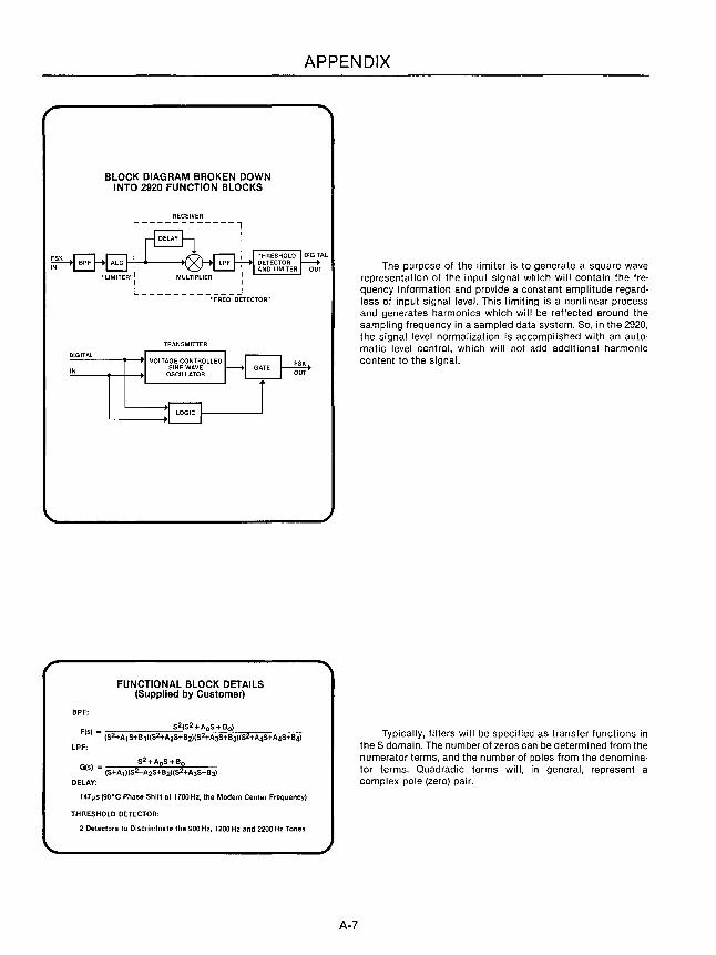
APPENDIX
BLOCK DIAGRAM BROKEN DOWN INTO 2920 FUNCTION BLOCKS
RECEIVER i------------l
"FREC DETECTOR"
TRANSMITIER
DIGITAL
~OLTAGECONTROLLED
IN ci'~~~L~~~ER
~~------~
~ FSK.
~
J
BPF:
F(s)
LPF:
FUNCTIONAL BLOCK DETAILS (Supplied by Customer)
G S2+AoS+Bo (5) = (S+A1)(S4A2S+B2l(S2+A3S+B3)
DELAY:
147,,5 (90'C Phase Shift at 1700Hz,the Modem Center Frequency)
THRESHOLD DETECTOR:
2 Detectors to Dlscrlmlnato the 900 Hz, 1200 Hz and 2200 Hz Tones
A-7
The purpose of the limiter is to generate a square wave representation of the input signal which will contain the frequency information and provide a constant amplitude regardless of input signal level. This limiting is a nonlinear process and generates harmonics which will be reflected around the sampling frequency in a sampled data system. 80, in the 2920, the signal level normalization is accomplished with an automatic level control, which will not add additional harmonic content to the signal.
Typically, filters will be specified as transfer functions in the 8 domain. The number of zeros can be determined from the numerator terms, and the number of poles from the denominator terms. Quadradic terms will, in general, represent a complex pole (zero) pair.
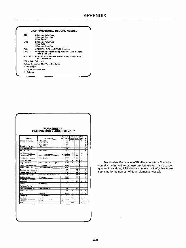
,. 2920 FUNCTIONAL BLOCKS NEEDED
BPF: 4 Complex Pole Pairs 1 Complex Zero Pair 2 Real Zeros
LPF: 2 Complex Pole Pairs 1 Real Pole 1 Complex Zero Pair
AlC: Simple Pole Filter and Divide Algorithm DELAY: 2 Register Delay Line: Delay will be 1471's II Sample
Rate is 13.6 kHz MULTIPLY: 9 Bit x 25 Bit (9 Bits are Adequate Because of 9 Bit
AID Conversion) 2 Threshold Detectors
Voltage Controlled Sine Wave Oscillator 1 9 Bit Input 2 Digital Inputs (1 Bit)
2 Outputs
WORKSHEET #1 2920 BUILDING BLOCK SUMMARY
"Of " 01 Total " Tolal
APPENDIX
Function Comments Inst's Inst's RAM RAM DAR
4 Qu.drant Multiply
20uadran! Multiply
ConstanlMulliply
4 Quadrant DIVide
Complex Pole Pair
16 Bit )(25 Bit 9 BII )(25 Bit
12 18 26 10
Complex Zero Pa., When hnked with pole/separate 2 5 10(7 1
Full Quadrant S.cllon Pole + Zero Pllr 1222 34
Singl. Real Pol. 26 12
\lngl. Real Zero When hnked with pole/separate 2
2 Cascaded Qu.dradlcs 2 Pole + Zero Pairs
J Pole, 2 Zero Filler 1 Real and 1 Complex Pole
Sawtooth Wave Generator 37
Tnangle Wave Generalor
SlneW,vaGenerator
SLO Sweeping
'1CO (voltage controlled oscillator)
Full Wave Rectifier
Trapezoidal Waveform (5% THD)
Sine Wave
FWR + Single Pole LPF Envelope detector
Threshold Detector
Ale DIVide +LPF
Unit Delay 1 Sample Period
Subtotal
Overhead
TOTAL
1120
8%
14 27
152
A-8
To calculate the number of RAM locations for a filter which contains poles and zeros, use the formula for the cascaded quadradic sections, # RAM = n + 2, where n = # of poles (corresponding to the number of delay elements needed).
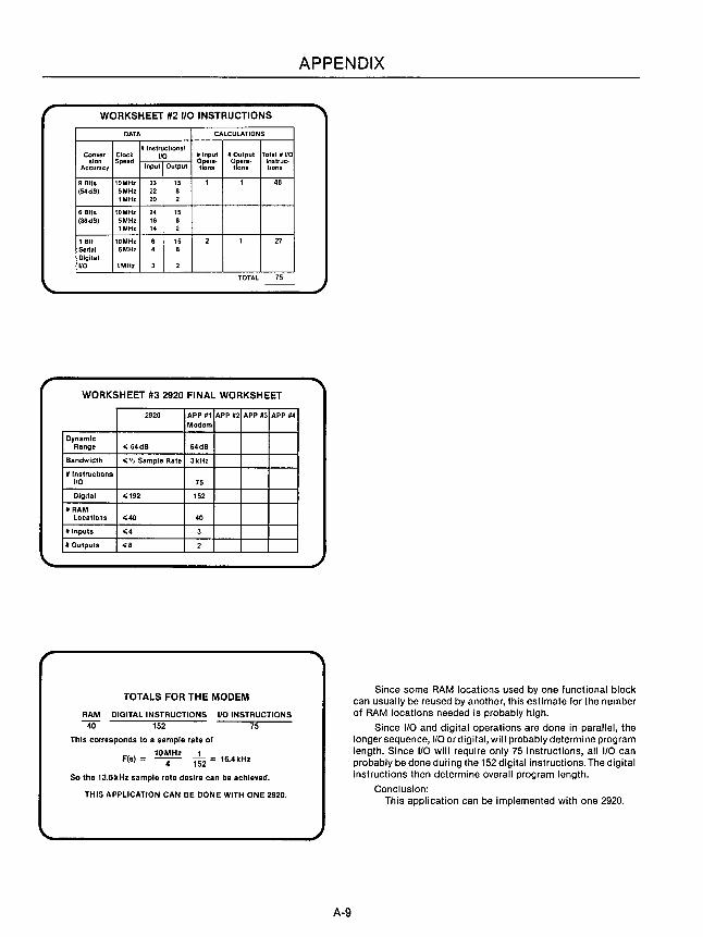
WORKSHEET #2 1/0 INSTRUCTIONS
DATA CALCULATIONS
N Inslrucllonsl Conver Clock 110 N Input N Outpul Tolal N 1/0
slon Speed Input Oulpul ~ro~:· ~ro~:· Instruc·
Accuracy lions
9 Blls 10MHz 33 15 1 1 48 (54 dB) 5MHz 22 8
lMHz 20 2
6 Blls 10MHz 24 15 (36dB) 5MHz 16 8
lMHz 14 2
1 BII 10MHz 6 15 2 1 27 Serial 5MHz 4 8 Dlgllal 110 lMHz 3 2
TOTAL 75
WORKSHEET #3 2920 FINAL WORKSHEET
2920 APP #1 APP #2 APP #3 APP #4 Modem
Dynamic Range .. 54dB 54dB
Bandwidth .. y, Sample Rate 3kHz
II Instructions 1/0 75
Digital .. ,92 152
# RAM locations .. 40 40
# Inputs .. 4 3
# Outputs .. 8 2
TOTALS FOR THE MODEM
RAM DIGITAL INSTRUCTIONS 1/0 INSTRUCTIONS 40 152 75
This corresponds to a sample rate of
10MHz 1 F(s) = -4- 152 = 16.4kHz
So the 13.6kHz sample rate desire can be achieved.
THIS APPLICATION CAN BE DONE WITH ONE 2920.
APPENDIX
A-9
Since some RAM locations used by one functional block can usually be reused by another, this estimate for the number of RAM locations needed is probably high.
Since I/O and digital operations are done in parallel, the longer sequence, I/O or digital, will probably determine program length. Since 1/0 will require only 75 instructions, all I/O can probably be done during the 152 digital instructions. The digital instructions then determine overall program length.
Conclusion: This application can be implemented with one 2920.

REFERENCES
(1) "An Analog Input/Output Microprocessor for Signal Processing", M. E. Hoff, M. Townsend, IEEE International Solid State Circuits Digest of Technical Papers, Feb. 1979; Pg. 220.
(2) "Single Chip NMOS Microcomputer Processes Signals in Real Time", M. E. Hoff, M. Townsend, Electronics, March 1, 1979, Pg. 105.
(3) "First Single Chip Signal Processor Simplifies Analog Design Problems", Robert Holm, Electronic Design, Sept. 27,1979, Pg. 50.
(4) "Program a Spectrum Analyzer on a One Chip Real Time Signal Processor", Robert Holm, Electronic Design, Nov. 8,1979, Pg. 70.
(5) "Development System Facilitates Programming of Signal-Processor Chip", Charles Yager, Electronic Design, Dec. 6, 1979, Pg. 106.
(6) "Implement Complex Analog Filters With a Real Time Signal Processor", Robert Holm, EDN, Nov. 20, 1979.
(7) "Software Makes a Big Talker Out of the 2920", M. E. Hoff, Wallace Li, Electronics, Jan. 31, 1980, Pg. 102.
(8) "An NMOS Microprocessor for Analog Signal Processing", M. Townsend, M. E. Hoff, R. Holm, IEEE Journal of Solid State Circuits, Feb. 1980.
(9) "A Single Chip NMOS Signal Processor", M. Townsend, M. E. Hoff, IEEE-ICASSP, 1980, DSP 5.7.
(10) "An Analog Microcomputer for Signal Processing", M. Townsend, M. E. Hoff, National Telecommunications Conference, 11/28/79, Session 25.
(11) "An Analog Microcomputer", M. E. Hoff, M. Townsend, Wescon 1980 Processional Program, Session 16.4.
(12) "A New Approach to Analog Design Using the 2920 Programmable Analog Signal Processor", Robert E. Holm, ED Design Series, June 1980.
(13) "Modulation, Noise, and Spectral Analysis", Philip F. Panter, McGraw-Hill Book Company, 1965.
(14) "Digital Filters: Analysis and Design", Andreas Antoniou, McGraw-Hill Book Company, 1979.
(15) "Digital Signal Processing", William D. Stanley, Prentice-Hall, Company, 1975.
(16) "Theory and Application of Digital Signal Processing", Lawren~e R. Rabiner, Bernard Gold, Prentice-Hall, Inc., 1975.
(17) "Digital Signal Processing", Alan V. Oppenheim, Ronald W. Schafer, Prentice-Hall, Inc., 1975.


illtel~ 3065 Bowers Avenue Santa Clara, California 95051 Tel' (408) 987-8080 TWX: 910-338-0026 TELEX: 34-6372
ALABAMA
Inlel Corp. 303 Williams Avenue, S W Sulle 1422 Huntsville 35801 Tel (205) 533·9353
ARIZONA
Intel Corp 10210 N 25th Avenue, Suite 11 Phoenix 85021 Tel (602) 997·9695
BFA 4426 Nonh Saddle Bag Trail Scottsdale 85251 Tel (602) 994-5400
CALIFORNIA
Intel Corp 7670 opponunlty Rd Suite 135 San Doego 92111 Tel (714) 268-3563
Inlel Corp' 2000 East 4th Street Suite 100 Santa Ana 92705 Tel (714) 835-9642 TWX 91()'595-1114
Intel Corp' 15335 MOrrison SUite 345 Sherman Oaks 91403 Tel (213) 986 9510 TWX 91()'495-2045
Intel Corp' 3375 Scott Blvd Santa Clara 95051 Tel (408) 987-8086 TWX 91 ()'339·9279
91 ()'338'()255
Earle ASSOCiates, Inc 4617 Rullner Street SUite 202 San Diego 92111 Tel (714) 278·5441
Mac I 2576 Shattuck Ave SUite 4B Berkeley 94704 Tel (415) 843·7625
Mac I POBox 1420 Cupenlno 95014 Tel (408) 257·9880
Macl 558 Valley Way Calaveras BUSiness Par1t Milpitas 95035 Tel (408) 946-8885
Mac·1 PO Box 87G3 Fountain Valley 92708 Tel (714) 839-3341
Mac·1 1321 Centlnela Avenue SUite 1 Santa Monica 90404 Tel (213) 829-4797
Mac·1 20121 Ventura Blvd, Suite 240E Woodland Hills 91364 Tel (213) 347 5900
COLORADO
Intel Corp' 650 5 Cherry Street SUite 720 Denver 80222 Tel (303) 321-11088 TWX 91()'931·2289
Westek Data Product., Inc 25921 Fern Gulch POBox 1355 Evergreen 80439 Tel (303) 874 5255
Wostek Data Products, Inc 1322 Arapahoe Boulder 80302 Tel (303) 449-2620
Westek Data Products, Inc 1228 W Hinsdale Or Littleton 80120 Tel (303) 797.Q482
u.s. AND CANADIAN SALES OFFICES
CONNECTICUT
Intel Corp Peacock Alley 36 Padanaram Road Danbury 06810 Tel (203) 792·8366 TWX 710456 1199
FLORIDA
Intel Corp 1001 N W 62nd Street, SUite 406 Ft Lauderdale 33309 Tel (305) 771-0600 TWX 51()'956 9407
Intel Corp 5151 Adanson Sireet, SUite 203 Orlando 32804 Tel (305) 628-2393 TWl( 81().853·9219
ILLINOIS
Intel Corp' 2550 Golf Road, Suite 815 Roiling Meadows 60008 Tel (312) 981-7200 TWX 910-651·5861
Technical Representallv, 1502 Nonh Linde Street Bloomington 61701 Tel (309) 629-8080
INDIANA
Intel Corp 9101 Wesleyan Road Suite 204 Indianapolis 46268 Tel (317) 299.()623
IOWA
Technical Representatives, Inc St Andrews Building 1930 St Andrews Drive N E Cedar Rapids 52405 Tel (319) 393·5510
KANSAS
Intel Corp 9393 W 110th St ,Ste 265 Overland Park 68210 Tel (913) 642·8080
Technical Representatives, Inc 8245 Nieman Road, SUite 100 Lenexa 68214 Tel (913) 868-0212, 3, & 4 TWX 91()'749-6412
Technical Representat,ves, Inc 360 N Rock Road SUite 4 Wichita 67206 Tel (316) 681'()242
MARYLAND
Intel Corp' 7257 Parkway Drive Hanover 21076 Tel (301) 796-7500 TWX 710-862·1944
Mesa Inc 16021 Industrial Dr Gaithersburg 20760 Tel (301) 448·4350
MASSACHUSETTS
Intel Corp' 27 Industrial Ave Chelmsford 01824 Tel (617) 867 8126 TWX 71 ()'343-6333
EMCCorp 381 Elliot Street Newton 02164 Tel (617) 244-4740 TWX 922531
MICHIGAN
Intel Corp' 26500 Nonhwestern Hwy Suite 401 Southfield 48075 Tel (313) 353.()92O TWX 81()'244·4915
MINNESOTA
Intel Corp 7401 Metro Blvd Suite 355 Edina 55435 Tel (612) 835-8722 TWX 91()'576-2867
MISSOURI
Intel Corp 502 Eanh City Plaza Suite 121 Eanh City 63045 Tel (314) 291·1990
Technical Representatives, Inc· 502 Eanh City Plaza, SUite 201 Eanh City 63045 Tel (314)291·0001
Technical Representatives, Inc· VSW Bldg SUite 560 406 W 31st Street Kansas City 64111 Tel (816) 756·3575
NEW JERSEY
Intel Corp' Raritan Plaza 2nd Floor Raritan Center Edison 08617 Tel (201) 225-3000 TWX 710-480-6238
NEW MEXICO
BFA Corporation 1704 Moon N E , SUite 7 Las Cruces 87112 Tel (505) 523.Q601 TWX 91()'983'()543
BFA Corporation 3705 Westerfield, N E Albuquerque 87111 Tel (505) 292·1212 TWX 910·989·1157
NEW YORK
Intel Corp' 300 Motor Pkwy Hauppauge 11787 Tel (516) 231·3300 TWX 510·227-6236
Intel Corp 80 Washington St PoughkeepSie 12601 Tel (914) 473-2303 TWX 510·248'()060
Intel Corp' 2255 Lyell Avenue Lower Floor East SUite Rochester 14606 Tel (716) 254-6120 TWX 51()'253-7391
Measurement Technology. Inc 159 Nonhem Boulevard Great Neck 11021 Tel (516) 482·3500
T·Squared .054 Newcourt Avenue Syracuse 13206 Tel (315) 463-8592 TWX 71()'541'()554
T·Squared 2 E Main Victor 14564 Tel (716) 924·9101 TWX 51()'254-8542
NORTH CAROLINA
Intel Corp 154 Huffman Mill Rd Burlington 27215 Tel (919) 564·3631
OHIO
Intel Corp' 6500 Poe Avenue Dayton 45415 Tel (513) 89().5350 TWX 810-45().2528
Intel Corp' Chagrin Brainard Bldg, No 300 28001 Chagrin Blvd Cleveland 44122 Tel (216) 464·2736 TWX 81()'427·9298
OREGON
Intet Corp 10700 S W Beaverton Hillsdale Highway SUite 324 Beavenon 97005 Tel (503) 641-8086 TWX 910-467-8741
PENNSYLVANIA
Intel Corp' 275 Commerce Dr 200 Olflce Center SUite 300 Fon Washington 19034 Tel (215) 542·9«4 TWX 51().681·2077
Intel Corp· 201 Penn Center Boulevard SUite 301W Pittsburgh 15235 Tel (412) 823 4970
QED Electronics 300 N York Road Hatboro 19040 Tel (215) 674·9600
TEXAS
Intel Corp' 2925 LB J Freeway SUite 175 Dalla. 75234 Tel (214) 241·9521 TWX 91 ().86()'5617
Intel Corp' 6420 Richmond Ave SUite 280 Houston 77057 Tel (713) 784·3400 TWX 91().S81·2490
Industrial Digital Systems Corp 5925 Sovereign SUite 101 Houston 77036 Tel (713) 988·9421
Intel Corp 313 E Anderson Lane SUite 314 Austin 78752 Tel (512) 454·3628
WASHINGTON
Intel Corp SUite 114, Bldg 3 1603 116th Ave N E Bellevue 98005 Tel (206) 453-8088 TWX 91 ()'443·3OO2
WISCONSIN
Intel Corp 150 S Sunnyslope Rd Brookfield 53005 Tel (414) 764·9060
CANADA
Intel Semiconductor Corp .. SUite 233, Bell Mews 39 Highway 7, Bells Corners Ottawa, Ontario K2H 8R2 Tel (613) 829·9714 TELEX 053-4115
Intel Semiconductor Corp 50 Galaxy Blvd Unit 12 Rexdale, Ontario M9W4Y5 Tel (416) 675-2105 TELEX 06983574
Mullllek,lnc' 15 Grenfell Crescent Ottawa, Ontario K2G OG3 Tel (613) 226-2365 TELEX 053-4565
Multllek,lnc Toronto Tel (416) 245-4622
Mulhfek, Inc Montreal lei (514) 481-1350
'Field Appllcatron Location

3065 Bowers Avenue Santa Clara, California 95051 Tel. (408) 987-8080 TWX: 910-338-0026 TELEX: 34-6372
ALABAMA
tHamliton/Avnet Electronics 4812 Commercial Drive N.W. Huntsville 35805 Tel. (205) 837-7210
tPloneer/Huntsvllle 1207 Putman Drive NW HuntSVille 35805 Tel: (205) 837·9033 TWX: 810-726·2197
ARIZONA
tHamllton/Avnet Electronics 505 S Madison Drive Tempe 85281 Tel (602) 275-7851
tWyle Distribution Group 8155 N 24th Avenue Phoenix 85021 Tel. (602) 249-2232 TWX: 910-951-4282
CALIFORNIA
Arrow Electronics, Inc 9511 Ridge Haven Court San Diego 92123 Tel: (714) 565-4800
Arrow Electronics, Inc 720 Pa,omar Avenue Sunnyvale, California 94086 Tel. (408) 739·3011
t Avnet Electronics 350 McCormick Avenue Costa Mesa 92626 Tel: (714) 754-6111 TWX· 910-595-1928
tAvnet Electronics 4942 Rosecrans Ave. Hawthorne 90250 Tel: (213) 970-0956
Hamllton/Avnet Electronics 1175 Bordeaux Dr Sunnyvale 94086 Tel. (408) 743-3355 TWX 910-339·9332
tHamliton/Avnet ElectroniCS 4545 View ridge Ave. San Diego 92123 Tel· (714) 571·7510 TWX: 910-335·1216
tHamliton/Avnet ElectroniCS 10950 W. Washington Blvd. Culver City 90230 Tel: (213) 558-2809 TWX· 910-340-6364 or 7073
Hamllton/Avnet Electronics 3170 Pullman Costa Mesa 92626 Tel. (714) 641-1850
tHamllton Electro Sales 3170 Pullman Street Costa Mesa 92626 Tel: (714) 641-4100
tWyle Distribution Group 124 Maryland Street EI Segundo 90245 Tel: (213) 322·3826 TWX: 910-348-7140 or 7111
tWyle Distribution Group 9525 Chesapeake Dr. San Diego 92123 Tel: (714) 565-9171 TWX. 910-335-1590
tWyle Distribution Group 3000 Bowers Avenue Santa Clara 95052 Tel. (408) 727·2500 TWX: 910-338-{)451 or 0296
Wyle Distribution Group 17872 Cowan Avenue Irvine 92714 Tel: (714) 641·1611
u.s. AND CANADIAN DISTRIBUTORS
COLORADO
tWyle Distribution Group 6777 E 50th Avenue Commerce City 80022 Tel (303) 287-9611 TWX: 910·931-{)510
tHamllton/Avnet Electronics 8765 E. Orchard Road SUite 708 Englewood 80111 Tel: (303) 740-1000 TWX: 910-931-{)510
CONNECTICUT
tArrow Electronics 12 Beaumont Road Wallingford 06492 Tel· (203) 265-7741 TWX: 710-476-{)162
tHamliton/Avnet Electronics Commerce Industrial Park Commerce Drive Danbury 06810 Tel (203) 797-2800
tHarvey Electronics 112 Main Street Norwalk 06851 Tel (203) 853-1515 TWX: 710-468·3373
FLORIDA
tArrow ElectroniCS 1001 N.W. 62nd Street Suite 108 Ft. Lauderdale 33309 Tel. (305) 776-7790
tArrow Electronics 115 Palm Bay Road, NW Suite 10, Bldg 200 Palm Bay 32905 Tel. (305) 725-1480 TWX: 510-959-6337
tHamliton/Avnet ElectroniCS 6800 Northwest 20th Ave. FI. Lauderdale 33309 Tel (305) 971·2900 TWX: 510·955-3097
Hamllton/Avnet Electronics 3197 TeCh. Drive North SI. Petersburg 33702 Tel. (813) 576-3930 TWX: 810-863-{)374
tPloneer/Orlando 6220 S Orange Blossom Trail SUite 412 Orlando 32809 Tel· (305) 859·3600 TWX: 810-850-{)177
GEORGIA
Arrow Electronics 2979 Pacific Drive Norcross 30071 Tel: (404) 449-8252 TWX: 810·757-4213
tHamliton/Avnet Electronics 6700 1-85 Access Road, No. 11 Suite lE Norcross 30071 Tel (404) 448-{)800
ILLINOIS
Arrow Electronics 492 Lunt Avenue P.O Box 94248 Schaumburg 60193 Tel. (312) 893·9420 TWX. 910-222-1807
tHamliton/Avnet Electronics 3901 No. 25th Avenue Schiller Park 60176 Tel. (312) 678-6310 TWX 910-227-{)060
ILLINOIS (conL)
Pioneer/Chicago 1551 Carmen Drive Elk Grove 60007 Tel. (312) 437·9680 TWX: 910-222·1834
INDIANA
tPloneerllndlana 6408 Castleplace Drive Indianapolis 46250 Tel: (317) 849-7300 TWX: 810·260-1794
KANSAS
tHamliton/Avnet ElectroniCS 9219 Qulvlra Road Overland Park 66215 Tel. (913) 888-8900
tComponent Specialties, Inc. 8369 Nieman Road Lenexa 66214 Tel: (913) 492·3555
MARYLAND
Arrow ElectroniCS, Inc. 4801 Benson Avenue Baltimore 21227 Tel: (301) 247-5200
tHamliton/Avnet Electronics 7235 Standard Drive Hanover 21076 Tel (301) 796-5684 TWX: 710-862·1861
tPloneer/Washlngton 9100 Gaither Road Gaithersburg 20760 Tel: (301) 948-{)710 TWX· 710-828-{)545
MASSACHUSETTS
tHamliton/Avnet Electronics 50 Tower Ollice Park Woburn 01801 Te I (617) 273-7500
tArrow Electronics 96D Commerce Way Woburn 01801 Tel. (617) 933-8130
Harvey/Boston 44 Hartwell Ave. Lexington 02173 Tel (617) 861-9200
MICHIGAN
tArrow ElectroniCS 3810 Varsity Drive Ann Arbor 48104 Tel: (313) 971-8220 TWX. 810-223-6020
t Pioneer/ Michigan 13485 Stamford Livonia 48150 Tel. (313) 525-1800 TWX: 810-242-3271
tHamliton/Avnet ElectroniCS 32487 Schoolcraft Road Livonia 48150 Tel: (313) 522-4700 TWX. 810·242-8775
MINNESOTA
tArrow ElectroniCS 5230 W. 73rd Street Edina 55435 Tel: (612) 830-1800 TWX: 910-576·2726
tlndustrial Components 5229 Edina Industrial Blvd MinneapoliS 55435 Tel: (612) 831-2666 TWX: 910-576-3153
MINNESOTA (con!.)
tHamllton/Avnet ElectroniCS 7449 Cahill Road Edina 55435 Tel: (612) 941·3801 TWX: 910·576-2720
MISSOURI
tHamllton/Avnet Electronics 396 Brookes Lane Hazelwood 63042 Tel: (314) 344-1200 TWX 910-762-{)606
NEW HAMPSHIRE
tArrow Electronics 1 Perimeter Drive Manchester 03103 Tel: (603) 66B-6968
NEW JERSEY
tArrow Electronics Pleasant Valley Avenue Moorestown 08057 Tel: (609) 235-1900 TWX: 710-897-{)829
tArrow ElectroniCS 285 Midland Avenue Saddle Brook 07662 Tel: (201) 797-5800 TWX: 710-988-2206
tHamliton/Avnet ElectroniCS 1 Keystone Ave. Bldg 36 Cherry Hili 08034 Tel: (609) 424-{)100 !WX· 710-897-1405
t Harvey ElectroniCS 45 Route 46 Plnebrook 07058 Tel: (201) 575-3510 TWX. 710-734-4382
Hamllton/Avnet ElectroniCS 10 Industrial Road Fairfield 07006 Tel: (201) 575-3390 TWX: 710-734-4338
NEW MEXICO
t Alliance ElectroniCS Inc. 11721 Central Ave. N.E. Albuquerque 87123 Tel: (505) 292-3360 TWX· 910-989-1151
tHamllton/Avnet Electronic! 2524 Baylor Drive, S.E. Albuquerque 87106 Tel: 15051765-1500
NEW YORK
Arrow ElectroniCS 900 Broad Hollow Road Farmingdale 11735 Tel: (516) 694-6800 TWX: 510-224-6494
fArrow Electronics 3000 South Winton Road Rochester 14623 Tel: (716) 275-0300 TWX 910-338-{)026
fArrow Electronics 7705 Maltlage Drive Liverpool 13088 Tel. (315) 652-1000 TWX· 710-545-{)230
Arrow ElectroniCS 20 Oser Avenue Hauppauge 11787 Tel (516) 231-1000 TWX· 510-224-6494 tHamlltonlAvnet Electronics 167 Clay Road Rochester 14623 Tel: (716) 475-9130 TWX. 910-340-8364
tMlcrocomputer System Technical Demonstrator Centers

3065 Bowers Avenue Santa Clara, California 95051 Tel. (408) 987-8080 TWX: 910-338-0026 TELEX: 34-6372
NEW YORK (cont.)
tHamliton/Avnet Electronics 16 Corporate Circle E. Syracuse 13057 Tel: (315) 437·2641
tHamliton/Avnet Electronics 5 Hub Drive Melville, Long Island 11746 Tel' (516) 454-6000 TWX: 510-252'()893
Harvey Electronics P.O. Box 1208 Blnghampton 13902 Tel: (607) 748-8211 TWX: 510-252'()893
t Harvey Electronics 60 Crossways Park West Woodbury 11797 Tel: (516) 921-8700 TWX: 510-221·2184
Harvey/Rochester 840 Fairport Park Fairport 14450 Tel: (716) 381-7070
NORTH CAROLINA
Arrow Electronics 938 Burke Street Winston-Salem 27102 Tel: (919) 725-8711 TWX: 510-922-4765
Pioneer/Carolina 106 Industrial Ave. Greensboro 27406 Tel' (919) 273-4441 TWX: 510-925-1114
tHamliton/Avnet Electronics 2803 Industrial Drive Raleigh 27609 Tel' (919) 829-8030
OHIO
Arrow Electronics 7620 McEwen Road Centerville 45459 Tel: (513) 435-5563 TWX: 810-459-1611
Arrow Electronics 6238 Cochran Ad. Solon 44139 Tel: (216) 248-3990
Arrow Electronics 10 Knollcrest Dr. Cincinnati 45237 Tel: (513) 761-5432 TWX: 810-461-2670
tHamillon/Avnet Electronics 954 Senate Drive Dayton 45459 Tel: (513) 433-0610 TWX: 910-340-2531
tHamlitonlAvnet Electronics 4588 Emery Industrial Parkway Warrensville Heights 44128 Tel: (216) 831-3500
tPloneer/Dayton 1900 Troy Street Dayton 45404 Tel: (513) 238-9900 TWX: 810-459-1622
t Pioneer/Cleveland 4800 E. 131st Street Cleveland 44105 Tel: (216) 587-3600 TWX. 810-422·2210
u.s. AND CANADIAN DISTRIBUTORS
OKLAHOMA
tComponents Speclalllfls, Inc. 7920 E. 40th Street Tulsa 74145 Tel: (918) 664-2820 TWX: 910-845-2215
OREGON
tAlmaclStroum Electronics 8022 S W. Nimbus, Bldg. 7 Beaverton 97005 Tel: (503) 841-9070
tHamillon/Avnet Electronics 6024 SW Jean Ad. Bldg. C, Suite 10 Lake Oswego 97034 Tel: (503) 635-8157
PENNSYLVANIA
tArrow Electronics 4297 Greensburg Pike Suite 3114 Pittsburgh 15221 Tel: (412) 351-4000
Pioneer/Pittsburgh 560 Alpha Drive Pittsburgh 15238 Tel: (412) 782-2300 TWX: 710-795-3122
Pioneer/Delaware Valley 141 Gibraltar Road Horsham 19044 Tel. (215) 674-4000 TWX: 510-665-8778
TENNESSEE
tArrow Electronics P.O. Box 129 W. Andrew Johnson Hwy. Talbl)lI 37677 Tel: (815) 587-2137
TEXAS
Arrow Electronics 13715 Gamma Road Dallas 75234 Tel: (214) 388-7500 TWX: 910-861-5495
Arrow Electronics, Inc. 10700 Corporate Drive, Suite 100 Stallord 77477 Tel: (713) 491-4100
Component Specialties Inc. 8222 Jamestown Drive Suite 115 Austin 78757 Tel: (512) 837-8922 TWX' 910-874-1320
tComponent Specialties, Inc. 10907 Shady Trail, Suite 101 Dallas 75220 Tel: (214) 357-8511 TWX: 910-861-4999
tComponent Specialties, Inc. 8585 Commerce Park Drive, suite 590 Houston 77036 Tel: (713) 771-7237 TWX: 910-881-2422
Hamillon/Avnet Electronics 10508A Boyer Blvd. Austin 78757 Tel: (512) 837-8911
tHamliton/Avnet Electronics 4445 Sigma Road Dallas 75240 Tel: (214) 661-8661 TWX: 910-860-5371
tHamliton/Avnet Electronics 3939 Ann Arbor Drive Houston 77063 Tel: (713) 780-1771
UTAH
tHamliton/Avnet Electronics 1585 West 2110 South Salt Lake City 84119 Tel: (801) 972-2800
WASHINGTON
tAlmaclStroum Electronics 5811 Sixth Ave. South Seattle 98108 Tel: (206) 763-2300 TWX: 910-444-2067
Arrow Electronics, Inc. Electronics Distribution Division 1059 Andover Park East Tukwila 98188 Tel: (206) 575'()907
tHamllton/Avnet Electronics 14212 N.E. 21st Street Bellevue 98005 Tel: (206) 453-5844
tWyle Distribution Group 1750 132nd Avenue NE Bellevue 98005 Tel: (206) 453-8300 TWX: 910-443-2526
WISCONSIN
tArrow Electronics 430 W. Rawson Avenue Oak Creek 53154 Tel: (414) 784-6600 TWX: 910-338.()026
tHamliton/Avnet Electronics 2975 Moorland Road New Berlin 53151 Tel: (414) 784-4510 TWX: 910-262-1182
CANADA
ALBERTA
tL.A. Varah Ltd. 4742 14th Street N.E. Calgary T2E 6L7 Tel: (403) 230-1235 TWX: 018-258-97
Zentronlcs 9224 27th Avenue Edmonton T6N 1 B2
Zentronlcs 3651 21st N.E. Calgary T2E 6T5 Tel: (403) 230-1422
BRITISH COLUMBIA
tL.A. Varah Ltd. 2077 Alberta Street Vancouver V5Y 1C4 Tel: (604) 873-3211 TWX: 610-929-1066
Zentronlcs 550 Camble SI. Vancouver V6B 2N7 Tel: (604) 688-2533 TWX: 04-5077-89
MANITOBA
L.A. Varah 1-1832 King Edward Street Winnipeg R2R ON1 Tel: (204) 633-8190 TWX: 07-55-365
Zentronlcs 590 Berry St. Winnipeg R3H OS1 Tel: (204) 775-8881
ONTARIO
tHamliton/Avnet Electronics 3888 Nashua Drive, Units G & H Mlsslssauga L4V 1M5 Tel: (416) 677-7432 TWX: 610-492-8860
tHamliton/Avnet Electronics 1735 Courtwood Crescent Ottawa K2C 3J2 Tel: (613) 226-1700
tL.A. Varah, Ltd. 505 Kenora Avenue Hamilton L8E 3P2 Tel: (416) 581-9311 TWX: 061-8349
tZentronlcs 141 Catherine Street Ottawa K2P 1 C3 Tel: (613) 238-6411 TWX. 053-3636
tZentronlcs 1355 Meyerslde Drive Mississauga, Ontario L5T 1C9 Tel: (416) 676-9000 Telex: 06-983-657
QUEBEC
tHamliton/Avnet Electronics 2670 Sabourin Street SI. Laurent H4S 1 M2 Tel: (514) 331-6443 TWX: 610-421-3731
Zentronlcs 5010 Pare Street Montreal H4P 1 P3 Tel: (514) 735-5381 TWX: 05-827-535
tMlcrocomputer System Technical Demonstrator Center.

intJ 3065 Bowers Avenue INTERNATIONAL SALES AND MARKETING OFFICES Santa Clara, California 95051 Tel: (408) 987-8080 TWX: 910-338-0026 TELEX: 34-6372
INTERNATIONAL DISTRIBUTORS/REPRESENTATIVES
ARGENTINA
Micro Sistemas SA 9 De Julio 561 Cordoba Tel' 54·51-32-880 TELEX' 51837 BICCO
AUSTRALIA
A J F. Systems & Components Pty. Ltd. 310 Queen Street Melbourne Victoria 3000 Tel' TELEX.
Warburton Frankl Corporate Headquarters 372 Eastern Valley Way Chatswood, New South Wales 2067 Tel 407·3261 TELEX: AA 21299
AUSTRIA
Bacher Elektronlsche Geraete GmbH Rotenmulgasse 26 A 1120 Vienna Tel' (0222) 83 63 96 TELEX: (01) 1532
Reklrsch Elektronlk Geraete GmbH Llchtenstelnstrasse 97 Al000 Vienna Tel. (222) 347646 TELEX. 74759
BELGIUM
Inelco Belgium S A. Ave. des Croix de Guerre 94 Bl120 Brussels Tel. (02) 2160160 TELEX: 25441
BRAZIL
Icotron S.A. 0511·Av. Mutinga 3650 6 Andar Plrltuba-Sao Paulo Tel 261'()211 TELEX: (011) 222 ICO BR
CHILE
DIN Av. Vic. Mc kenna 204 Cas Ilia 6055 Santiago Tel: 227564 TELEX: 3520003
CHINA
C.M. Technologies 525 University Avenue Suite A·40 Palo Alto, CA 94301
COLOMBIA
International Computer Machines Adpo Aereo 19403 Bogota 1 Tel. 232-6635 TELEX 43439
CYPRUS
Cyprus Eltrom Electronics P.O. Box 5393 NICOSIa Tel: 21·27982
DENMARK
STL-Lyngso Komponent AlS Ostmarken 4 DK-2860 Soborg Tel: (01) 6700 77 TELEX: 22990
Scandinavian Semiconductor Supply AlS Nannasgade 18 DK·2200 Copenhagen Tel. (01) 835090 TELEX' 19037
FINLAND
Oy Flntronlc AB Melkonkatu 24 A SF'()0210 Helsinki 21 Tel. 0.fj926022 TELEX' 124224 IOtron SF
FRANCE
Celdls SA." 53, Rue Charles Frerot F·9425O Gentllly Tel: (1) 581 00 20 TELEX 200 485
Feutrler Rue des TrOIS Glorleuses F-42270 SI. Prlest-en-Jarez Tel: (77) 74 67 33 TELEX 300 0 21
Metrologle" La Tour d'Asnleres 4, Avenue Laurent Cely 92606-Asnleres Tel' 791 44 44 TELEX: 611 448
Tekelec Alrtronlc" Cite des Bruyeres Rue Carle Vernet F·92310 Sevres Tel. (1) 534 7535 TELEX' 204552
GERMANY
Electronic 2000 Vertrlebs GmbH Neumarkter Strasse 75 D-8000 Munich 80 Tel. (089) 434061 TELEX' 522561
Jermyn GmbH Postfach 1180 D.fj077 Cam berg Tel. (06434) 231 TELEX' 484426
Kontron Elektronlk GmbH Breslauerstrasse 2 8057 Echlng B 0-8000 Munich Tel. (89) 319 011 TELEX: 522122
Neye Enatechnlk GmbH Schillerstrasse 14 0·2085 Qulckborn·Hamburg Tel. (04106) 6121 TELEX: 02-13590
GREECE
American Technical Enterprises P.O Box 156 Athens Tel 30-1·8811271
30-Hl219470
HONG KONG
Schmidt & Co. 28/F Wing on Center Connaught Road Hong Kong Tel 5-45~44 TELEX' 74766 Schmc Hx
INDIA
Mlcronlc Devices 104/109C, Nlrmal Industrial Estate Slon(E) Bombay 400022, IndIa Tel' 486-170 TELEX' 011·5947 MDEV IN
ISRAEL
Eastronlcs Ltd " 11 Rozanls Street P.O Box 39300 Tel Aviv 61390 Tel: 475151 TELEX: 33638
ITALY
Eledra 3S S.P A." Vlale Elvezla, 18 120154 Milan Tel: (02) 34 93.041-31.85.441 TELEX' 332332
JAPAN
Asahl Electronics Co. Ltd. KMM Bldg. Room 407 2·14·1 Asano, Kokura Klta·Ku, Kltokyushu City 802 Tel: (093) 511.fj471 TELEX. AECKY 7126-16
Hamllton·Avnet Electronics Japan Ltd. YU and YOU Bldg. 1·4 Horldome·Cho Nlhonbashl Tel: (03) 662·9911 TELEX. 2523774
Ryoyo ElectriC Corp Konwa Bldg 1·12·22, TsuklJI, l-Chome Chuo·Ku, Tokyo 104 Tel (03) 543·7711
Tokyo Electron Ltd. No.1 Hlgashlkata·Machl Mldorl-Ku, Yokohama 226 Tel: (045) 471·8811 TELEX. 781-4473
KOREA
Koram Digital Room 909 Woonam Bldg. 7, l-KA Bongre·Dong Chung·Ku Seoul Tel' 23-8123 TELEX: K23542 HANSINT
Leewood International, Inc. C P.O Box 4046 112·25, Sokong·Dong Chung·Ku, Seoul 100 Tel. 26-5927 CABLE' "LEEWOOD" Seoul
NETHERLANDS
Inelco Nether. Compo Sys. BV Turfstekerstraat 63 Aalsmeer 1431 0 Tel (2977) 28855 TELEX: 14693
Koning & Hartman Koperwerf 30 2544 EN Den Haag Tel. (70) 210.101 TELEX: 31528
NEW ZEALAND
W. K McLean Ltd. PO. Box 16-065 Glenn Innes, Auckland, 6 Tel' 587'()37 TELEX. NZ2763 KOSFY
NORWAY
Nordlsk Elektronlk (Norge) AlS Postoffice Box 122 Smedsvlngen 4 1364 Hvalstad Tel' 02786210 TELEX 17546
PORTUGAL
Dltram Componentes E Electronlca LOA Av. MIguel Bombarda, 133 Llsboa 1 Tel: (19) 545313 TELEX: 14347 GESPIC
SINGAPORE
General Engineers Associates Blk 3, 1003-1008, 10th Floor P.S.A. Multl·Storey Complex Telok Blangah/Paslr Panjang Smgapore 5 Tel 271-3163 TELEX RS23987 GENERCO
SOUTH AFRICA
Electronic Building Elements Pine Square 18th Street Hazelwood, Pretoria 0001 Tel 789221 TELEX: 30181SA
SPAIN
Interface S.A Ronda San Pedro 22, 3" Barcelona 10 Tel: 301 78 51 TWX: 51508
ITT SESA Miguel Angel 16 Madrid 10 Tel. (1) 4190957 TELEX' 27707/27461
SWEDEN
AB Gosta Backstrom Box 12009 10221 Stockholm Tel (08) 541 080 TELEX. 10135
Nordlsk Electronlk AB Box 27301 S-10254 Stockholm Tel (08) 635040 TELEX. 10547
SWITZERLAND
Industrade AG Gemsenstrasse 2 Postcheck 80 - 21190 CH-8021 Zurich Tel: (01) 60 22 30 TELEX: 56788
TAIWAN
Taiwan Automation Co." 3d Floor 1175, Section 4 Nanking East Road Taipei Tel' 771'()940 TELEX: 11942 TAIAUTO
TURKEY
Turkelek Electronics Apapurk Boulevard 169 Ankara Tel: 189483
UNITED KINGDOM
Comway Mlcrosystems Ltd. Market Street 66-Bracknell, Berkshire Tel: (344) 51654 TELEX. 847201
G E.C. Semiconductors Ltd. East Lane North Wembley Middlesex HA9 7PP Tel: (01) 904·9303/906-4111 TELEX: 28817
Jermyn Industries Vestry Estate Sevenoaks, Kent Tel: (0732) 501.44 TELEX: 95142
Rapid Recall, Ltd. 6 Soho Mills Ind. Park Woobum Green Bucks, England Tel; (6285) 24961 TELEX 849439
Sintrom ElectroniCS Ltd." Arkwright Road 2 Reading, Berkshire RG2 OLS Te I (0734) 85464 TELEX' 847395
VENEZUELA
Componente, y Clrcultos Electronlcos TTLCA C A.
Apartado 3223 Caracas 101 Tel: 716-100 TELEX: 21795 TELETIPOS
"Field Application Location

3065 Bowers Avenue INTERNATIONAL SALES AND MARKETING OFFICES Santa Clara, California 95051 Tel. (408) 987-8080 TWX: 91()'338'()()26 TELEX: 34-6372
INTEL~ MARKETING OFFICES
AUSTRALIA
Intel Australia Suite 2, Level 15, Nonh Point 100 Miller Street North Sydney, NSVII, 2060 Tel: 450-847 TELEX: AA 20097
BELGIUM
Intel Corporation SA. Rue du Moulin a Papler 51 BOlte 1 B·1160 Brussels Tel. (02) 660 30 10 TELEX: 24814
DENMARK
Intel Denmark AlS' Lyngbyvej 32 2nd Floor DK·2100 Copenhagen East Tel. (01) 18 20 00 TELEX. 19567
FINLAND
Intel Scandinavia Sentnenkuja 3 SF· 00400 Helsinki 40 Tel: (0) 558531 TELEX: 123 332
FRANCE
Intel Corporation, S.A.R L: 5 Place de la Balance Sillc 223 94528 Rungls Cedex Tel. (01) 687 22 21 TELEX' 270475
GERMANY
Intel Semiconductor GmbH' Seldlstrasse 27 8000 Muenchen 2 Tel: (089) 53 891 TELEX: 523 177
Intel Semiconductor GmbH Malnzer Strasse 75 6200 VII lesbaden 1 Tel: (06121) 700874 TELEX: 04186183
Intel Semiconductor GmbH VIIernerstrasse 67 P.O. Box 1460 7012 Fellbach Tel: (0711) 580082 TELEX: 7254826
Intel Semiconductor GmbH Hlndenburgstrasse 28/29 3000 Hannover 1 Tel: (0511)852051 TELEX: 923625
HONG KONG
Intel Tradmg Corporation 99-105 Des Voeux Rd., Central 18F, Unit B Hong Kong Tel. 5-450-647 TELEX: 63869
ISRAEL
Intel Semiconductor Ltd.' P.O. Box 2404 Haifa Tel. 972/452 4261 TELEX: 92246511
ITALY
Intel Corporation /lalla, S p.A. Corso Semplone 39 1·20145 Milano Tel: 2/34.93287 TELEX. 311271
JAPAN
Intel Japan K.K.' Flower Hill·Shmmachl East Bldg. 1·23-9, Shinmachl, Setagaya-ku Tokyo 154 Tel. (03) 426·9261 TELEX: 781·28426
NETHERLANDS
Intel Semiconductor B.V. Cometongebouw VIIestblaak 106 3012 Km Rotterdam Tel' (10) 149122 TELEX. 22283
NORWAY
Intel Norway AlS P.O. Box 92 Hvamvelen 4 N·2013 Skjetten Tel: (2) 742420 TELEX: 18018
SWEDEN
Intel Sweden A.B ' Box 20092 Alpvagen 17 S·16120 Bromma Tel: (08) 98 53 90 TELEX: 12261
SWITZERLAND
Intel Semiconductor A.G. Forchstrasse 95 CH 8032 Zurich Tel: 1·554502 TELEX: 557 89 Ich ch
UNITED KINGDOM
Intel Corporation (U.K.) Ltd. Broadfleld House 4 Between Towns Road Cowley, Oxford OX4 3NB Tel: (0865) 77 14 31 TELEX: 837203
Intel Corporation (U.K.) Ltd.' 5 Hospital Street Nantwlch, Cheshire CW5 5RE Tel. (0270) 62 65 60 TELEX: 38620
Intel Corporation (U.K.) Ltd. Dorcan House Eldlne Dnve Swlndon, Wiltshire SN3 3TU Tel: (0793) 26101 TELEX' 444447 INT SWN
'Field Application Location

inter 3065 Bowers Avenue Santa Clara, California 95051 Tel. (408) 987-8080 TWX: 910-338-0026 TELEX' 34-6372
CALIFORNIA
Intel Corp. 1601 Old Bayshore Hwy Suite 345 Burlingame 94010 Tel (415) 692-4762 TWX: 910-375-3310
Intel Corp 2000 E. 4th Street Suite 100 Santa Ana 92705 Tel' (714) 835-9642 TWX: 910-595-1114
Intel Corp. 7670 Opportunity Road San Diego 92111 Tel (714) 268-3563
Intel Corp. 3375 Scott 8lvd. Santa Clara 95051 Tel. (408) 987-8086
Intel Corp. 15335 Morrison Sherman Oaks 91403 Tel' (213) 986-9510
COLORADO
Intel Corp. 650 South Cherry Suite 720 Denver, 80222 Tel: (303) 321-8086 TWX. 910-931-2289
FLORIDA
Intel Corp. 1001 N.W 62nd Street SUite 406 Ft Lauderdale 33309 Tel: (305) 771-()600 TWX: 510-956-9407
ILLINOIS
Intel Corp. 2550 Golf Road Suite 815 Roiling Meadows 60008 Tel: (312) 981-7230 TWX' 910-253-1825
KANSAS
Intel Corp. 9393 W 110th Street SUite 265 Overland Park 66210 Tel' (913) 642-8080
MARYLAND
Intel Corp. 7257 Parkway Drive Hanover 21076 Tel: (301) 796-7500 TWX: 710-862-1944
u.s. AND CANADIAN SERVICE OFFICES
MASSACHUSETTS
Intel Corp. 27 Industrial Avenue Chelmsford 01824 Tel (617) 667-8126 TWX' 710-343-6333
MICHIGAN
Intel Corp. 26500 Northwestern Hwy. Suite 401 Southfield 48075 Tel: (313) 353.0920 TWX' 810-244-4915
MINNESOTA
Intel Corp 7401 Metro Blvd. Suite 355 Edina 55435 Tel (612) 835-6722 TWX. 910-576-2867
MISSOURI
Intel Corp 502 Earth City Plaza Suite 121 Earth City 63045 Tel (314) 291-1990
NEW JERSEY
Intel Corp. 2450 Lemoine Avenue Ft. Lee 07024 Tel. (201) 947-6267 TWX: 710-991-8593
OHIO
Intel Corp Chagrin-Brainard Bldg 11210 28001 Chagrin Blvd. Cleveland 44122 Tel: (216) 464-2736 TWX' 810-427-9298
Intel Corp. 6500 Poe Avenue Dayton 45414 Tel. (513) 890-5350 TWX' 810-450-2528
OREGON
Intel Corp. 10700 S W. Beaverton-Hillsdale Hwy. Bldg 2, Suite 324 Beaverton 97005 Tel: (503) 641-8086 TWX: 910-467-8741
PENNSYLVANIA
Intel Corp 275 Commerce Drive 200 Office Center Suite 300 Fort Washington 19034 Tel' (215) 542-9444 TWX. 510-651-2077
TEXAS
Intel Corp 313 E. Anderson Lane Suite 314 Austin 78752 Tel: (512) 454-3628 TWX: 91o-B74-1347
Intel Corp 2925 L.B.J. Freeway Suite 175 Dallas 75234 Tel: (214) 241-2820 TWX: 910-860-5617
Intel Corp. 6420 Richmond Avenue Suite 280 Houston 77057 Tel: (713) 784-1300 TWX: 910-881-2490
VIRGINIA
Intel Corp. 7700 Leesburg Pike Suite 412 Falls Church 22043 Tel' (703) 734-9707 TWX. 710-931.Q625
WASHINGTON
Intel Corp 1603116th Ave. N E SUite 114 Bellevue 98005 Tel: (206) 232-7823 TWX 910-443-3002
WISCONSIN
Intel Corp. 150 S. Sunnyslope Road Suite 148 Brookfield 53005 Tel (414) 784-9060
CANADA
Intel Corp. 50 Galaxy Blvd. Unit 12 Rexdale, Ontario M9W4Y5 Tel. (416) 675-2105 Telex: 069-83574
Intel Corp. 39 Hwy. 7, Bells Corners Ottawa, Ontario K2H 8R2 Tel (613) 829-9714 Telex' 053-4115

BUSINESS REPLY CARD FIRST CLASS PERMIT NO. 621, SANTA CLARA, CA
Pos.tage will be paid by Addressee:
Intel Corporation Attn: Literature Department 3065 Bowers Avenue Santa Clara, California 95051
III NO POSTAGE NECESSARY IF MAILED
IN THE u.S.
I'd like to receive free information on the following Intel products: o 16-Bit Microprocessors 0 EPROMs o 8-Bit Microprocessors 0 Signal Processors o Single-Chip Microcontrollers 0 Bubble Memories o Peripheral Controllers 0 Single Board Computers o Static RAMs 0 Dynamic RAMs 0 Development Systems o Telecom Products 0 Military Products
o Software High-Level Languages ( __________ __
o Macro Assemblers o Operating Systems
(RMX 80/86™) o Workshops
Additionally, I'd like to receive free: I have a need in months for the following Intel Products.
o Intel's Literature Catalog Lists Intel's major technical catalogs and manuals.
I have an immediate requirement. Please contact me. My application is __________________ _
I'd like to purchase the following catalogs: o MCS-86™ Family User's Manual - $7.50 o 1980 Component Data Catalog - $7.50 o 1980 Systems Data Catalog - $5.00 o Peripheral Design Handbook - $7.50 (Prices are subject to change without notice.) To order send check, money order or use your VISA or MasterCard. Account No. _________ __ o VISA 0 MasterCard Expiration Date _________ _
Product Quantity Product Quantity
Name: ______________________________________________ _
Title: ____________________________ __
Company: __________________________ __
Address: ______________________________ _
City, State: ____________________________ _
Zip: Telephone:
...., intor delivers solutions~

![ABB · 2018. 5. 10. · Technology Conference,Proceedings Vol.2 (1994),Pages 741-744. [2] H.Trankler, O.Kanoun, "Importance of Signal Pro-cessing in Sensor Systems", Technisches Messen](https://img.pdfslide.us/doc/110x75/610903282f84c27cec6d200b/abb-2018-5-10-technology-conferenceproceedings-vol2-1994pages-741-744.jpg)