Embed Size (px)
Citation preview
arX
iv:1
410.
0395
v1 [
cond
-mat
.mtr
l-sc
i] 1
Oct
201
4
Tuning the Structural, Electronic, and Magnetic Properties of
Germanene by the Adsorption of 3d Transition Metal Atoms
Thaneshwor P. Kaloni∗
Department of Chemistry, University of Manitoba, Winnipeg, MB, R3T 2N2, Canada
Abstract
The structural, electronic, and magnetic properties of 3d transition metal (TM) atoms (Sc, Ti,
V, Cr, Mn, Fe, Co, Ni, Cu, and Zn) adsorbed germanene are addressed using density functional
theory. Based on the adsorption energy, TM atoms prefer to occupy at the hollow site for all
the cases. The obtained values of the total magnetic moment vary from 0.97 µB to 4.95 µB in
case of Sc to Mn-adsorption, respectively. A gap of 74 meV with a strongly enhanced splitting of
67 meV is obtained in case of Sc-adsorption, whereas metallic states are obtained in case of Ti,
Cr, Mn, Fe, and Co. Non-magnetic states are realized for Ni, Cu, and Zn-adsorption. Moreover,
semiconducting nature is obtained for non-magnetic cases with a gap of 26 to 28 meV. Importantly,
it is found that V-adsorbed germanene can host the quantum anomalous Hall effect. The obtained
results demonstrate that TM atoms and nearest neighbour Ge atoms are ferro-magnetically ordered
in the cases of V, Mn, Fe, Co, Ni, Cu, and Zn, while anti-ferromagnetic ordering is obtained for Sc,
Ti, and Cr. In addition, the effects of the coverage of all TM atoms on the electronic structure and
the ferro-magnetic and anti-ferro-magnetic coupling in case of Mn are examined. The results could
help to understand the effect of TM atoms in a new class of two-dimensional materials beyond
graphene and silicene.
Keywords: Two-dimensional, DFT calculations, Band gap, Quantum anomalous Hall effect
1
I. INTRODUCTION
Graphene is a material of interest particularly due to its unique electronic structure that
features the Dirac cone. It has been proposed to be a great candidate for the nanoelectronic
industry1,2. In contrast to these expectations, the mass production and band gap opening in
graphene are large hindrance. As consequence, its important to search for new classes of two-
dimensional (2D) materials. In recent years, silicene and germanene have been expected to
be counterparts of graphene3. Experimentally, the growth mechanism of silicene on metallic
substrates and its probable impact in electronic devices have been addressed4,5. A strong
interaction between the silicene and Ag metal by providing relatively large binding energy
of about 460 meV has been found4, which is very large as compared to the binding energy
of graphene on graphite (50 meV) and hence it would be difficult to exfoliate silicene from
the Ag substrate. On the other hand, the sublattice symmetry of the silicene is broken
due to the interaction of the silicene with ZrB2 and hence a larger band gap of about 0.25
eV has been realized5. Theoretically, the interaction of silicene with some semiconducting
substrates (SiC and h-BN) has also been studied and it has been predicted that free-standing
silicene can be realized on these substrates6,7. A smaller binding energy of about 57 meV7
to 100 meV6 has been realized for silicene on h-BN and SiC substrates, which indicates that
silicene can be exfoliated from these semiconducting substrates. As compared to C, Si, and
Ge have larger ionic radii and as a result they promote sp3 hybridization. The magnitude of
the buckling in silicene and germanene is 0.46 A and 0.68 A, respectively, which is a result
of the possible mixture of sp2 and sp3 hybridization in these materials. This buckling is
responsible for the tunable band gap8–10. In addition, the intrinsic spin orbit interaction
(SOI) of germanene is stronger than that for silicene and graphene. The magnitude of the
SOI is found to be 46.3 meV, 4 meV, and 1 µeV, for germanene, silicene, and graphene,
respectively11.
Recently, the growth of germanene on a GaAs(0001) substrate has been studied and
it has been predicted that H passivated GaAs(0001) would be a potential way to realize
quasi-free-standing germanene12. A single layer of germanene without H passivation of the
dangling Ga bonds is still strongly bound to the GaAs(0001), and as a result it would be
difficult to exfoilate the germanene in order to make it free-standing. The fact is that after
H intercalation between the interface of the germanene and GaAs(0001), it strongly reduces
2
the interaction between germanene and the GaAs(0001) resulting in a binding energy of
about 86 meV per Ge atom. In recent years, TM atoms doped graphene have been a
topic of great interest. It has been found that TM atoms induce doping, scattering13,
magnetism14, and superconduction15 at the limit of dilute concentration and strongly modify
the electronic structure at the limit of high concentration16,17. Moreover, TM atom doped
silicene has also been studied and it has been been demonstrated that 3d TMs bind more
strongly with silicene as compared to graphene and magnetism can be induced after doping
in silicene18. Importantly, TM-adsorbed silicene shows the quantum anomalous Hall states,
which is expected to be a potential candidate in spintronic devices19. Furthermore, Be, Mg,
and Ca-adsorbed silicene found to be a narrow gap semiconductor, while Ti and Cr-adsorbed
silicene have been found to be half-metal. It is expected that the half-metallic ferromagnetic
nature of Ti and Cr-adsorbed silicene could pave the way to build silicon-based spintronic
devices20.
The structural, electronic, and magnetic properties of TM atoms adsorbed germanene
have not been reported so far. However, from the electronic device applications point of
view, it is important to understand the behaviour of TM atoms adsorbed germanene. To
this aim, here we study Sc, Ti, V, Cr, Mn, Fe, Co, Ni, Cu, and Zn-adsorbed germanene in
comparison to each other in the framework of the density functional theory. We find that
Sc, Ti, V, Cr, Mn, Fe, and Co-adsorbed germanene induces magnetism, while non-magnetic
semiconducting states are realized for Ni, Cu, and Zn. It is found that Sc, Ni, Cu, and
Zn are semiconducting in nature with the largest gap of 74 meV for Sc-adsorption with a
strong band splitting of 67 meV. Moreover, the effect of the coverage of TM atoms on the
electronic structure has also been investigated. For the Mn doped case the ferro-magnetic
and anti-ferro-magnetic coupling is examined in order to understand the coupling between
two Mn atoms for variable distances. In addition, our results point out that V-adsorbed
germanene can host the quantum anomalous Hall effect.
II. COMPUTATIONAL DETAILS
All the calculations are performed using the generalized gradient approximation in the
Perdew-Burke-Ernzerhof parametrization (PBE).21 The van der Waals interactions are taken
into account in order to achieve the correct description of the long-range interaction and
3
hence dispersions (PBE-D)22, which should be included in multilayers of 2D systems23–26. A
plane wave cutoff energy of 540 eV and a Monkhorst-Pack 16× 16× 1 k-mesh are used. A
4×4×1 supercell of germanene with a lattice constant of a = 16.24 A and a vacuum layer of
15 A are used. The supercell contains 32 Ge atoms and 1 TM atom, which ensure that the
density of the impurities is low enough in order to neglect the mutual interaction between
TM atom impurities. The atomic positions are optimized until the forces have converged
about to 0.005 eV/A. In addition, SOI is taken into account in all the calculations because
germanene has stronger SOI of the order of 46.3 meV, which can not be neglected. It is well
known that a finite onsite Coulomb interaction is essential to get an accurate description of
atoms containing d electrons17,27, thus, we use an onsite Coulomb interaction of U = 4.0 eV
in our calculations.
III. GERMANENE
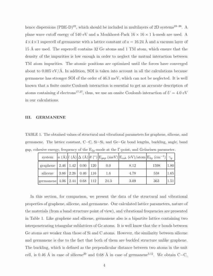
TABLE 1. The obtained values of structural and vibrational parameters for graphene, silicene, and
germanene. The lattice constant, C−C, Si−Si, and Ge−Ge bond lengths, buckling, angle, band
gap, cohesive energy, frequency of the E2g-mode at the Γ-point, and Gruneisen parameter.
system a (A) l (A) ∆ (A) θ (◦) Egap (meV) Ecoh (eV)/atom E2g (cm−1) γg
graphene 2.46 1.42 0.00 120 0.0 8.12 1598 1.80
silicene 3.86 2.26 0.46 116 1.6 4.78 558 1.65
germanene 4.06 2.44 0.68 112 24.3 3.09 363 1.51
In this section, for comparison, we present the data of the structural and vibrational
properties of graphene, silicene, and germanene. Our calculated lattice parameters, nature of
the materials (from a band structure point of view), and vibrational frequencies are presented
in Table 1. Like graphene and silicene, germanene also is a bipartite lattice containing two
interpenetrating triangular sublattices of Ge atoms. It is well know that the π bonds between
Ge atoms are weaker than those of Si and C atoms. However, the similarity between silicene
and germanene is due to the fact that both of them are buckled structure unlike graphene.
The buckling, which is defined as the perpendicular distance between two atoms in the unit
cell, is 0.46 A in case of silicene20 and 0.68 A in case of germanene3,12. We obtain C−C,
4
Γ K M Γ-1
-0.5
0
0.5
1
E-E
F (e
V)
Eg = 24.3 meV
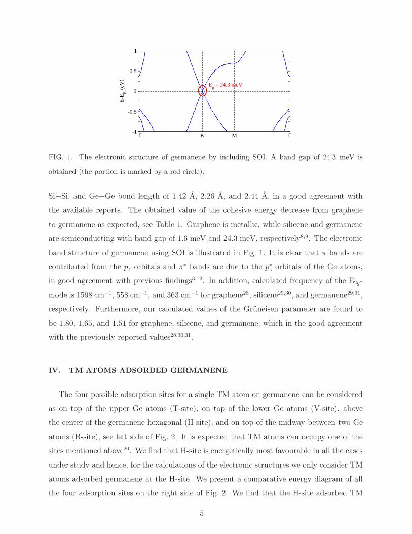
FIG. 1. The electronic structure of germanene by including SOI. A band gap of 24.3 meV is
obtained (the portion is marked by a red circle).
Si−Si, and Ge−Ge bond length of 1.42 A, 2.26 A, and 2.44 A, in a good agreement with
the available reports. The obtained value of the cohesive energy decrease from graphene
to germanene as expected, see Table 1. Graphene is metallic, while silicene and germanene
are semiconducting with band gap of 1.6 meV and 24.3 meV, respectively8,9. The electronic
band structure of germanene using SOI is illustrated in Fig. 1. It is clear that π bands are
contributed from the pz orbitals and π∗ bands are due to the p∗z orbitals of the Ge atoms,
in good agreement with previous findings3,12. In addition, calculated frequency of the E2g-
mode is 1598 cm−1, 558 cm−1, and 363 cm−1 for graphene28, silicene29,30, and germanene29,31,
respectively. Furthermore, our calculated values of the Gruneisen parameter are found to
be 1.80, 1.65, and 1.51 for graphene, silicene, and germanene, which in the good agreement
with the previously reported values28,30,31.
IV. TM ATOMS ADSORBED GERMANENE
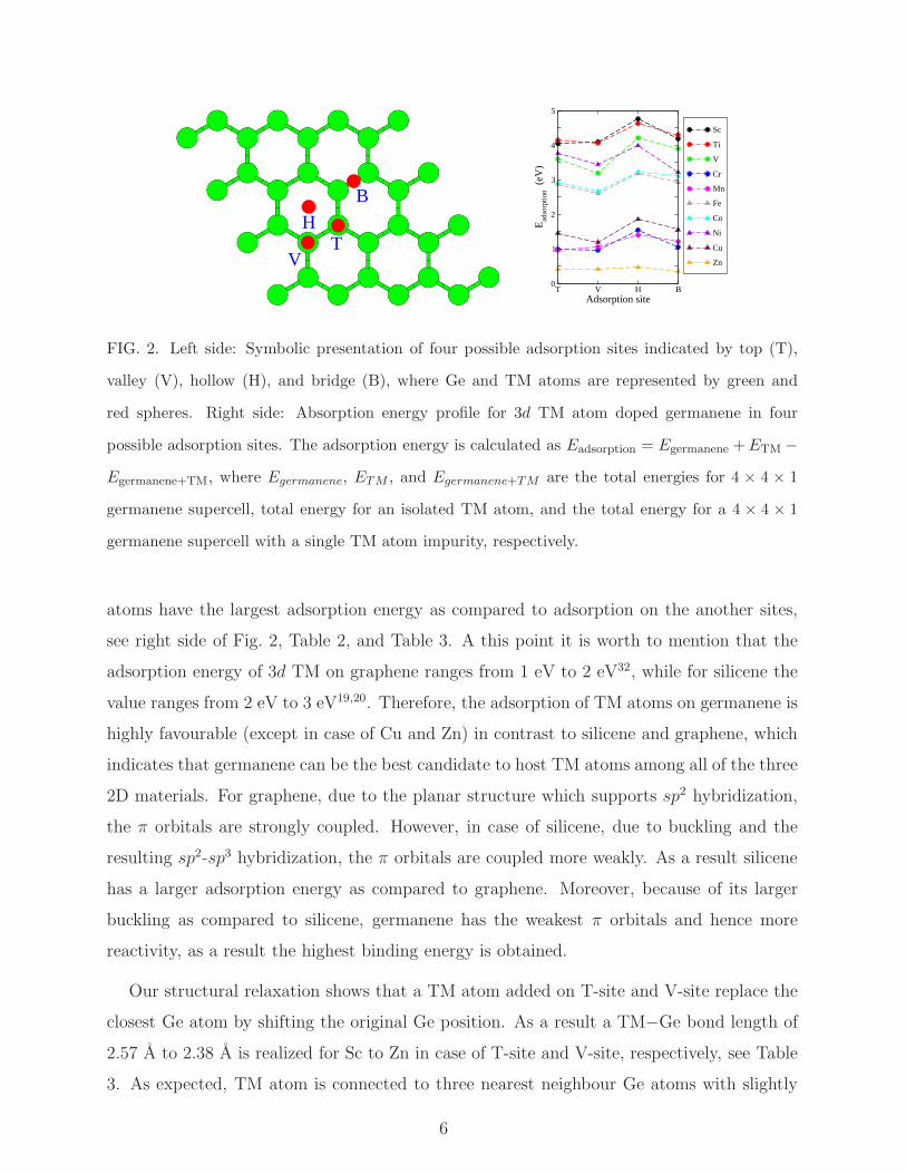
The four possible adsorption sites for a single TM atom on germanene can be considered
as on top of the upper Ge atoms (T-site), on top of the lower Ge atoms (V-site), above
the center of the germanene hexagonal (H-site), and on top of the midway between two Ge
atoms (B-site), see left side of Fig. 2. It is expected that TM atoms can occupy one of the
sites mentioned above20. We find that H-site is energetically most favourable in all the cases
under study and hence, for the calculations of the electronic structures we only consider TM
atoms adsorbed germanene at the H-site. We present a comparative energy diagram of all
the four adsorption sites on the right side of Fig. 2. We find that the H-site adsorbed TM
5
TH
B
V
T V H BAdsorption site
0
1
2
3
4
5
Ead
sorp
tion
(eV
)
Sc
Ti
V
Cr
Mn
Fe
Co
Ni
Cu
Zn
FIG. 2. Left side: Symbolic presentation of four possible adsorption sites indicated by top (T),
valley (V), hollow (H), and bridge (B), where Ge and TM atoms are represented by green and
red spheres. Right side: Absorption energy profile for 3d TM atom doped germanene in four
possible adsorption sites. The adsorption energy is calculated as Eadsorption = Egermanene +ETM −
Egermanene+TM, where Egermanene, ETM , and Egermanene+TM are the total energies for 4 × 4 × 1
germanene supercell, total energy for an isolated TM atom, and the total energy for a 4 × 4 × 1
germanene supercell with a single TM atom impurity, respectively.
atoms have the largest adsorption energy as compared to adsorption on the another sites,
see right side of Fig. 2, Table 2, and Table 3. A this point it is worth to mention that the
adsorption energy of 3d TM on graphene ranges from 1 eV to 2 eV32, while for silicene the
value ranges from 2 eV to 3 eV19,20. Therefore, the adsorption of TM atoms on germanene is
highly favourable (except in case of Cu and Zn) in contrast to silicene and graphene, which
indicates that germanene can be the best candidate to host TM atoms among all of the three
2D materials. For graphene, due to the planar structure which supports sp2 hybridization,
the π orbitals are strongly coupled. However, in case of silicene, due to buckling and the
resulting sp2-sp3 hybridization, the π orbitals are coupled more weakly. As a result silicene
has a larger adsorption energy as compared to graphene. Moreover, because of its larger
buckling as compared to silicene, germanene has the weakest π orbitals and hence more
reactivity, as a result the highest binding energy is obtained.
Our structural relaxation shows that a TM atom added on T-site and V-site replace the
closest Ge atom by shifting the original Ge position. As a result a TM−Ge bond length of
2.57 A to 2.38 A is realized for Sc to Zn in case of T-site and V-site, respectively, see Table
3. As expected, TM atom is connected to three nearest neighbour Ge atoms with slightly
6
TABLE 2. Dopant, the adsorption energy, the average distance of dopant form germanene sheet,
Ge−Ge bond length, buckling, angle, total magnetic moment per supercell, magnetic moment
contributed from 3d TM orbital, magnetic moment contributed from sum of all Ge atoms, nature
of the bands (m→metallic), and band splitting at the K point for TM atoms adsorbed on H-site.
dopantEadsorption
(eV)
d
(A)
Ge−Ge
(A)
∆
(A)
θ
(◦)
total
(µB)
3d
(µB)
Ge
(µB)
Egap
(meV)
Esp
(meV)
Sc 4.62 1.21 2.45-2.59 0.62-0.74 101-115 0.97 1.01 −0.04 74 67
Ti 4.46 0.71 2.45-2.61 0.64-0.76 100-111 1.13 1.99 −0.06 m –
V 4.21 0.69 2.45-2.71 0.61-0.75 95-111 3.01 2.92 0.09 1 19
Cr 1.55 0.65 2.45-2.63 0.66-0.71 95-111 4.00 4.05 −0.05 m 21
Mn 1.39 0.68 2.45-2.67 0.63-0.74 97-112 4.95 4.65 0.30 m 11
Fe 3.18 0.60 2.46-2.62 0.67-0.75 100-112 3.24 3.05 0.19 m 31
Co 3.22 0.98 2.48-2.81 0.61-0.76 78-111 1.10 1.05 0.05 m –
Ni 3.99 1.32 2.44-2.45 0.65-0.72 111-112 0.00 0.00 0.00 27 26
Cu 1.86 1.12 2.44-2.47 0.66-0.71 112-114 0.00 0.00 0.00 29 6
Zn 0.99 1.55 2.44-2.46 0.67-0.70 112-113 0.00 0.00 0.00 26 24
smaller bond length. This finding agrees well with the 3d TM atoms adsorbed silicene19. The
TM atom is located at the midway between two Ge atoms by providing a slight distortion
around the adsorption site in case of B-site adsorption. The TM atom occupies at the
centre of the Ge hexagon in case of H-site adsorption. Around the adsorption site, we find a
variable Ge−Ge bond lengths 2.45 A to 2.81 A for all the adsorbent, see Table 2. However,
the Ge−Ge bond length is slightly modified as compared to pristine germanene with a value
of 2.44 A3,12,20,31. The buckling in the germanene sheet varies from 0.61 A to 0.76 A. The
distance d, which is defined as the average height of TM atom from the germanene sheet is
vary from 0.60 A to 1.55 A, see Table 2, which agrees well with TM atoms adsorbed silicene
and graphene19,20,32. The obtained value of the angle (defined as the angle between Ge atom
to next Ge atom to third Ge atom) ranges from 95◦ to 115◦, for Sc to Zn, respectively.
7
TABLE 3. Dopant, TM−Ge bond length, and adsorption energy for T-site and V-site, respectively.
dopant TM−Ge (A) Eadsorption (eV)
T-site V-site T-site V-site
Sc 2.57 2.56 4.05 4.10
Ti 2.55 2.54 4.14 4.07
V 2.52 2.50 3.61 3.20
Cr 2.50 2.49 0.99 0.97
Mn 2.48 2.47 0.97 1.06
Fe 2.45 2.44 2.88 2.61
Co 2.44 2.42 2.92 2.67
Ni 2.42 2.41 3.77 3.45
Cu 2.40 2.39 1.46 1.20
Zn 2.39 2.37 0.41 0.42
Γ K M Γ-1
-0.5
0
0.5
1
E-E
F (e
V)
(a)
Γ K M Γ -1
-0.5
0
0.5
1
E-E
F (e
V)
(b)
Γ K M Γ -1
-0.5
0
0.5
1
E-E
F (e
V)
(c)
FIG. 3. Electronic structure (3d TM states are represented by dots) for (a) Sc, (b) Ti, and (c)
Cr-adsorbed germanene.
V. ELECTRONIC STRUCTURE
In this section, we analyse the electronic structure of TM atoms adsorbed germanene at
the energetically favourable H-site. Due to the charge redistribution between the 3d state
of the Sc and 4p state of the Ge atoms, the Dirac like point of the germanene shifts below
the Fermi level by 0.35 eV, see Fig. 3(a). The closer inspection of the partial partial density
8
of states (PDOSs) of the d orbital of Sc atom shows that the spin majority dz2, dxy, and
dyz as well as the spin minority d3r2 and dyz states contribute in the vicinity of the Fermi
energy, see Fig. 4(a). The system becomes n-type doped with a gap of 74 meV; this gap
could be shifted to the Fermi level such that system can be a perfect semiconductor19. A
stronger splitting of 67 meV is obtained, which agrees well with heavy atoms doped silicene36.
Experimentally, it is expected that the materials having large band splitting can have great
potential to construct spintronic devices34,35. The splitting is well distinguished from the
splitting in pristine germanene, which is due to the SOI between the valence and conduction
states. The double degeneracy of the valence and conduction bands is obtained by the SOI,
which in fact break the time-reversal symmetry. Hence, the gap opening is the consequences
of the sublattice symmetry breaking36. It is worth to mention that Sc-adsorbed silicene
does not have splitting because silicene has a weaker SOI as compared to germanene18.
Actually, there are two points which are interconnected. The band splitting is achieved due
to the combined SOI of silicene/germanene and dopant. Normally, the SOI increases with
increasing the size/atomic number of the atom. For example Au has the largest SOI among
C, Si, Sc, Ge, and Au. In case of Sc-adsorbed silicene the combined SOI would be smaller
than that of combined SOI of Au-adsorbed silicene, while combined SOI of Sc-adsorbed
germanene would be definitely larger than that of Sc-adsorbed silicene because the strength
of the SOI in germanene is 11 times higher than that in silicene. Note that the bands in
the vicinity of the Fermi level are contributed from Ge orbitals with no contribution from
Sc 3d orbitals. A total magnetic moment of 0.97 µB per supercell is obtained. The main
contribution of the magnetic moment comes Sc 3d states of 1.01 µB, whereas −0.04 µB
comes from the sum of all 33 Ge atoms. The obtained value of the total magnetic moment
shows a good agreement with the Sc-adsorbed silicene18. It should be noted that the host
germanene sheet is significantly polarized by leaving anti-ferro-magnetic alignment between
Sc and Ge atoms, which can be clearly understood by analysing the data presented in Table
2.
We obtain metallic nature of the bands for Ti-adsorbed germanene. It is clear that the
bands in the Fermi level are contributed by Ge pz orbitals and bands at the energy range
of about −0.24 eV to −0.35 eV are contributed by Ti 3d orbitals, see Fig. 3(b). From
the PDOSs of the Ti 3d orbitals, its is found that the spin majority dz2, dxy, dxz, and dyz
orbitals contribute at the vicinity of the Fermi level together with the spin minority dxy
9
-1 0 1E-E
F (eV)
-2
-1
0
1
2
PDO
S (s
tate
s/eV
)
dz2
d3r
2
dxy
dxz
dyz
-1 0 1E-E
F (eV)
-1 0 1E-E
F (eV)
-1 0 1E-E
F (eV)
-1 0 1E-E
F (eV)
(a) (b) (c) (d) (e)
FIG. 4. The calculated partial density of states (PDOSs) of 3d orbitals for (a) Sc, (b) Ti, and
(c) Cr, (d) Mn, and (e) Fe-adsorbed germanene. The solid and dashed lines represent the spin
majority and minority, respectively.
and dyz orbitals, see Fig. 4(b). Here the gap in pz and p∗z is largely enhanced up to about
0.22 eV due to the interaction with the Ti atoms, which is responsible for breaking the
sublattice symmetry as compared to pristine germanene. In this case the total magnetic
moment of 1.93 µB per supercell is found, where Ti 3d and Ge contributions amount to
1.99 µB and −0.06 µB, respectively, see Table 2. The obtained value of the total magnetic
moment agrees well with a recent report33. The Ti-adsorbed germanene has been predicted
to be an interesting system due to the fact that the magnetic moment and the nature of
the material are significantly modified by a application of the perpendicular electric field.
With certain values of the electric field the system behaves as half-metallic, which could be
useful for spintronic devices33. Like as Sc-adsorption, Ti and Ge atoms are also anti-ferro-
magnetically ordered.
Γ K M Γ-1
-0.5
0
0.5
1
E-E
F (e
V)
(a)
Γ K M Γ-1
-0.5
0
0.5
1
E-E
F (e
V)
(c)
Γ K M Γ -1
-0.5
0
0.5
1
E-E
F (e
V)
(b)
FIG. 5. Electronic structure for (a) Mn, (b) Fe, and (c) Co-adsorbed germanene.
The electronic band structure of Cr-adsorbed germanene is addressed in Fig. 3(c). We
10
observe a strong hybridization between the Cr 3d states to Ge 4p states and as a result
contributions of the 3d states are achieved near the Fermi level. This implies that the
system is metallic. The obtained data for the PDOSs of the Cr 3d orbitals show that the
bands at the vicinity of the Fermi level are mainly contributed from the spin majority dz2,
d3r2 , dxy, dxz, and dyz orbitals, while a small contribution is coming from the spin minority
dxy orbital, see Fig. 4(c). A band splitting of 21 meV is obtained, which is quite close to
the band gap of pristine germenene. The total magnetic moment of 4.00 µB is obtained.
The contribution of the magnetic moment from the 3d and the average of 33 Ge atoms are
found to be 4.05 µB and −0.05 µB, respectively. Our result for the magnetic moment agrees
well with the Cr-adsorbed graphene and silicene19,20,37. Recently, Cr-adsorbed graphene has
been synthesized and the samples have been identified experimentally by analysing the shift
in the Raman D and G peaks38, which could also be possible for Cr-adsorbed germanene.
-1 0 1E-E
F (eV)
-2
-1
0
1
2
PDO
S (s
tate
s/eV
)
dz2
d3r
2
dxy
dxz
dyz
-1 0 1E-E
F (eV)
-1 0 1E-E
F (eV)
-1 0 1E-E
F (eV)
-1 0 1E-E
F (eV)
(a) (b) (c) (d) (e)
FIG. 6. The calculated PDOSs of 3d states for (a) Co, (b) Ni, and (c) Cu, (d) Zn, and (e)
V-adsorbed germanene. The solid and dashed lines represent the spin majority and minority,
respectively.
The electronic structure of Mn-adsorbed germanene is addressed in Fig. 5(a). The nature
of the bands is similar to Cr-adsorption. However, in this case, Mn 3d states are located
far from the Fermi level, and the bands around the Fermi level are contributed from the Ge
4p orbitals. The PDOSs of the Mn 3d orbitals addressed in Fig. 4(d) show that a minor
contribution of the spin majority dxy and spin minority dxy orbitals are located at the vicinity
of the Fermi level. A smaller band splitting of 11 meV is observed, which can be further
enhanced by the application of an electric field9. The total magnetic moment is found to be
4.95 µB, while the Mn d magnetic moment amounts to 4.65 µB and the Ge magnetic moment
is found to be 0.30 µB. This indicates that the Ge and the Mn atom are ferro-magnetically
11
ordered. We also obtain the metallic nature of the bands in case of Fe and Co-adsorbed
germanene, see Figs. 5(b-c). In case of Fe, the PDOSs of the Fe 3d orbitals show that the
bands near to the Fermi level are contributed by the spin majority dxy and spin minority dz2,
see Fig. 4(e). While for Co-adsorption, the spin majority dz2, d3r2 , and dxy orbitals as well
as dz2, d3r2, dxy, dxz, and dyz orbitals contribute the bands at the vicinity of the Fermi level,
see Fig. 6(a). A band splitting of 31 meV is obtained in case of Fe-adsorption but we are not
able to locate the band splitting in Co-adsorption due to strong hybridization (which causes
the destruction in the bands) between Co 3d and Ge 4p orbitals. Total magnetic moment
of 3.24 µB and 1.10 µB is obtained for Fe and Co-adsorption. The major contribution of
the magnetic moment comes from TM d orbitals (see Table 2) by keeping intact the ferro-
magnetic ordering between TM and Ge atoms. The obtained value of the magnetic moment
shows good agreement with TM atoms adsorbed silicene18,19.
Γ K M Γ -1
-0.5
0
0.5
1
E-E
F (e
V)
(a)
Γ K M Γ -1
-0.5
0
0.5
1
E-E
F (e
V)
(b)
Γ K M Γ -1
-0.5
0
0.5
1
E-E
F (e
V)
(c)
FIG. 7. Electronic structure for (a) Ni, (b) Cu, and (c) Zn-adsorbed germanene.
We obtain a perfect semiconducting nature of the electronic structure with a gap of 27
meV in case of Ni-adsorbed germanene, see Fig. 7(a). The contributions from the Ni 3d
states are located about 0.45 eV below the Fermi level, and they are coming from the spin
majority and minority dz2, dxy, and dyz orbitals, see Fig. 6(b). Furthermore, the obtained
gap can be enhanced by applying an electric field39. Importantly, a band splitting of 26 meV
is observed at the valence as well as conduction bands at the K-point. Such a splitting has
been observed experimentally and theoretically for Pb adsorbed on the Ge(111) surface and
it has been suggested that the materials having larger splitting can be utilized to develop
spintronic devices45. As expected, the system is found to be non-magnetic, which agrees
12
well with Ni-adsorbed silicene19. The electrons from the 4s2 orbital transfer to the 3d8 and
hence 3d orbitals become completely filled and no magnetism is induced. We also realize the
non-magnetic states in case of Cu-adsorption, see Fig. 7(b). In this case the Dirac like point
of pristine germanene is shifted below the Fermi level (by leaving n-doped states) about
0.36 eV by opening a gap of 28 meV, slightly higher than that of pristine germanene of 24.3
meV. The n-type doping is obtained due to minute charge redistribution between Cu and
nearest Ge atoms. Finally, we deal with Zn-adsorbed germanene, just like for graphene and
silicene, in this case we also obtain non-magnetic states with a gap of about 26 meV close
to the Fermi level, see Fig. 7(c). The fact is that the Zn atom is only weakly bound to the
germanene and hence has minimal effect; as a result the opening of a gap is close to that
of bare germanene. There is no charge redistribution between Ge and Zn atoms, which can
be easily seen from Table 2. Moreover, the calculated PDOSs show that the contribution
form Cu and Zn d orbitals are located far from the Fermi level, see Fig. 6(c-d), which clearly
indicates that the bands at the vicinity of the Fermi level are contributed from the Ge pz
and p∗z orbitals.
Γ K M Γ -1
-0.5
0
0.5
1
E-E
F (e
V)
(a)
Γ K M Γ -1
-0.5
0
0.5
1
E-E
F eV
)
(b)
Γ K M Γ-1
-0.5
0
0.5
1
E-E
F (eV
)
(c)
K -0.44
-0.4
-0.36
-0.32
-0.28
E-E
F (
eV)
δ = 1 meV
(d)
FIG. 8. Electronic structure of V-adsorbed germanene for (a) 2× 2× 1, (b) 4× 4× 1, (c) 5× 5× 1
supercells, and (d) the zoomed portion of the red circle marked in (b).
In this section, we discuss an important part of the results, i. e. V-adsorbed germanene
can host the quantum anomalous Hall effect. The quantum anomalous Hall effect arises
because of the combined effect of the exchange-field (coming from the magnetic impurities,
i.e. the V atom), which breaks the time-reversal symmetry, and the larger SOI (which
induces band inversion and opens a nontrival gap). This effect has been predicted for TM
atoms adsorbed topological insulators40. Previously, the quantum anomalous Hall effect
in graphene has been predicted41–44. Very recently, the quantum anomalous Hall effect has
been observed in graphene on the (111) surface of an antiferromagnetic insulator (BiFeO3)46.
13
In addition, this effect has also been observed for silicene18,19,47. We find the quantum
anomalous Hall effect only in case of V-adsorbed germanene; the combined effect of the
exchange-field due to the V atom and SOI is sufficient to break the time-reversal symmetry
and induce the band inversion, as a result the anomalous Hall effect is realized. Various
coverages (11.11%, 3.12%, and 2.01%) of the V atoms are calculated by considering 2×2×1,
4×4×1 and 5×5×1 supercells of germanene. It it observed that only the supercells equal
for or larger than 4 × 4 × 1 are able to induce the quantum anomalous Hall effect. This
indicates that the interaction between the V atom and its periodic image is low enough
such that the quantum anomalous Hall effect can not be suppressed19. We calculate the
electronic structure of the V-adsorbed germanene with the coverages mentioned above, see
Fig. 8. In Fig. 8(a), the band structure of a 2 × 2 × 1 supercell of germanene with one V
atom (concentration of the V atom is 11.11%) is calculated. The distance between the V
atom and its periodic images is 8.12 A. In this case the quantum anomalous Hall effect is
not observed due to the strong interaction between the V atoms, which probably destroy
the effect. The bands near the Fermi level contributions from both the V 3d orbitals and
Ge 4pz orbitals, see Fig. 8(a).
However, in case of smaller coverages of the V atoms (4×4×1 and 5×5×1 supercells) the
bands near the Fermi level are not modified strongly and the bands are essentially coming
from the Ge 4pz orbitals, see Fig. 8(b-c). The calculated PDOSs for the V 3d orbitals show
that the bands close to the Fermi level are contributed by the spin majority dyz and spin
minority dz2, d3r2 , and dxy orbitals, see Fig. 6(e). The distance between the V atom and its
periodic image is large enough at 16.24 A and 20.30 A, respectively for 4×4×1 and 5×5×1
supercells to avoid the interaction between the V atoms. Hence, the quantum anomalous
Hall effect is realized in the latter two cases. The quantum anomalous Hall states are located
below the Fermi level by about 0.3 eV and 0.25 eV, which is indicated by the red circle. The
zoomed portion of the red circle in Fig. 8(b) is presented in Fig. 8(d). We find a nontrivial
gap of δ = 1 meV, which agrees well with the recently calculated value of the δ for graphene
on BiFeO346.
14
TM1 TM2
FIG. 9. Symbolic presentation of the adsorption of two TM atoms on H-site, where Ge and TM
atoms are represented by green and red spheres. A double sided arrow shows the distance of 4.06
A between TM1 and TM2 atoms.
VI. EFFECT OF THE COVERAGE
The structure under consideration for two TM atoms (the concentration of TM atom is
about 6.25%) adsorbed germanene on H-site is depicted in Fig. 9. The distance between
TM1 and TM2 amounts to be ∼4.06 A, which is equivalent to the lattice constant of a
1×1×1 unit cell for germanene. In case of two Sc-adsorbed germanene, a strong distortion
in the structure is observed as compared to single Sc-adsorbed germanene. The symmetry
is broken due to the distortion, as a result a large direct/indirect band gap of 290/220
meV is achieved, see Fig. 10(a). The obtained value of the band gap is ∼ 12 times larger
than that of pristine germanene, which could be interesting for germanene based electronic
devices34. The bands close to the Fermi level are contributed from Ge pz orbitals, it has
been demonstrated that the bands near the Fermi level are mainly not contributed from
TM atom if the concentration of TM atom is low (∼16 %)48. A band gap of 40 meV is
obtained for two Ti-adsorbed germanene, see Fig. 10(b), while single Ti-adsorbed germanene
is metallic in nature as discussed in previous section. In case of two Cr-adsorption, the
Dirac like cone shifted above the Fermi level (120 meV) by leaving the p-doped states with
a band gap of 11 meV at the π and π∗ orbitals of Ge atoms, see Fig. 10(c). Whereas, the
metallic states are obtained for two Mn, Fe, and Co-adsorbed germanene (see Figs. 10(d-
f)), the bands are qualitatively similar to a single Mn, Fe, and Co-adsorption. Moreover,
15
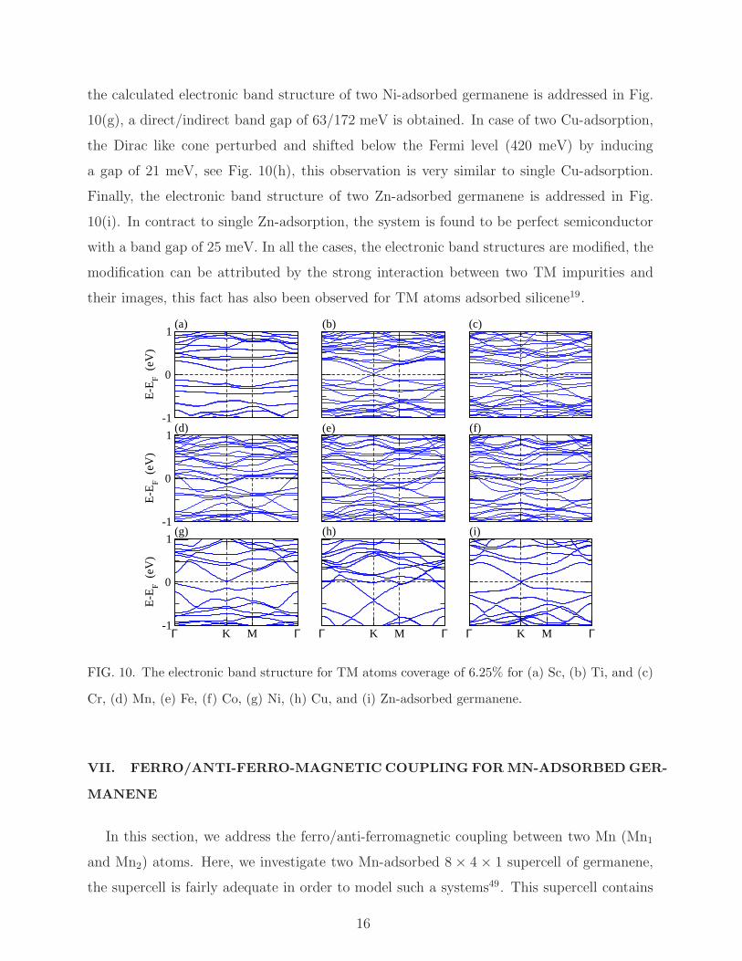
the calculated electronic band structure of two Ni-adsorbed germanene is addressed in Fig.
10(g), a direct/indirect band gap of 63/172 meV is obtained. In case of two Cu-adsorption,
the Dirac like cone perturbed and shifted below the Fermi level (420 meV) by inducing
a gap of 21 meV, see Fig. 10(h), this observation is very similar to single Cu-adsorption.
Finally, the electronic band structure of two Zn-adsorbed germanene is addressed in Fig.
10(i). In contract to single Zn-adsorption, the system is found to be perfect semiconductor
with a band gap of 25 meV. In all the cases, the electronic band structures are modified, the
modification can be attributed by the strong interaction between two TM impurities and
their images, this fact has also been observed for TM atoms adsorbed silicene19.
-1
0
1
E-E
F (eV
)
-1
0
1
E-E
F (eV
)
Γ K M Γ-1
0
1
E-E
F (eV
)
Γ K M Γ Γ K M Γ
(a)
(d)
(g)
(b)
(e)
(h) (i)
(f)
(c)
FIG. 10. The electronic band structure for TM atoms coverage of 6.25% for (a) Sc, (b) Ti, and (c)
Cr, (d) Mn, (e) Fe, (f) Co, (g) Ni, (h) Cu, and (i) Zn-adsorbed germanene.
VII. FERRO/ANTI-FERRO-MAGNETIC COUPLING FORMN-ADSORBED GER-
MANENE
In this section, we address the ferro/anti-ferromagnetic coupling between two Mn (Mn1
and Mn2) atoms. Here, we investigate two Mn-adsorbed 8 × 4 × 1 supercell of germanene,
the supercell is fairly adequate in order to model such a systems49. This supercell contains
16
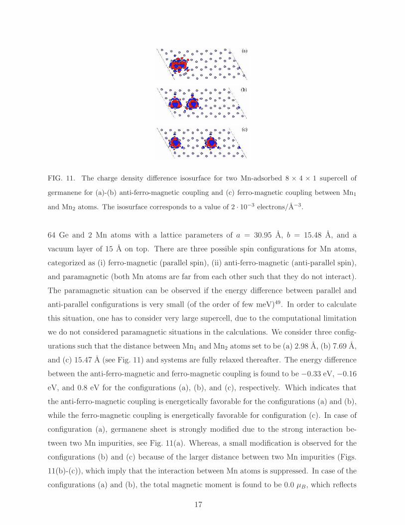
FIG. 11. The charge density difference isosurface for two Mn-adsorbed 8 × 4 × 1 supercell of
germanene for (a)-(b) anti-ferro-magnetic coupling and (c) ferro-magnetic coupling between Mn1
and Mn2 atoms. The isosurface corresponds to a value of 2 · 10−3 electrons/A−3.
64 Ge and 2 Mn atoms with a lattice parameters of a = 30.95 A, b = 15.48 A, and a
vacuum layer of 15 A on top. There are three possible spin configurations for Mn atoms,
categorized as (i) ferro-magnetic (parallel spin), (ii) anti-ferro-magnetic (anti-parallel spin),
and paramagnetic (both Mn atoms are far from each other such that they do not interact).
The paramagnetic situation can be observed if the energy difference between parallel and
anti-parallel configurations is very small (of the order of few meV)49. In order to calculate
this situation, one has to consider very large supercell, due to the computational limitation
we do not considered paramagnetic situations in the calculations. We consider three config-
urations such that the distance between Mn1 and Mn2 atoms set to be (a) 2.98 A, (b) 7.69 A,
and (c) 15.47 A (see Fig. 11) and systems are fully relaxed thereafter. The energy difference
between the anti-ferro-magnetic and ferro-magnetic coupling is found to be −0.33 eV, −0.16
eV, and 0.8 eV for the configurations (a), (b), and (c), respectively. Which indicates that
the anti-ferro-magnetic coupling is energetically favorable for the configurations (a) and (b),
while the ferro-magnetic coupling is energetically favorable for configuration (c). In case of
configuration (a), germanene sheet is strongly modified due to the strong interaction be-
tween two Mn impurities, see Fig. 11(a). Whereas, a small modification is observed for the
configurations (b) and (c) because of the larger distance between two Mn impurities (Figs.
11(b)-(c)), which imply that the interaction between Mn atoms is suppressed. In case of the
configurations (a) and (b), the total magnetic moment is found to be 0.0 µB, which reflects
17
the anti-ferro-magnetic coupling between Mn1 and Mn2 atoms, see the calculated charge
density isosurface. However, in case of configuration (c) the total magnetic moment is found
to be double than that of single Mn-adsorbed germanene, indicating the ferro-magnetic cou-
pling, see Fig. 11(c). For configuration (c), see Fig. 11(c), the isosurface for both Mn1 and
Mn2 atoms is exactly same, which is not a case for anti-ferro-magnetic coupling, compare
Figs. 11(a)-(b). Thus, anti-ferro-magnetic coupling is energetically favorable if the distance
between two Mn atoms is about 7.69 A, while ferro-magnetic coupling seems to be energet-
ically favorable if two Mn atoms are separated by a large distance of about 15.47 A. These
findings are quantitatively matching with Mn doped graphene49.
VIII. CONCLUSION
In conclusion, based on the first-principles calculations, we report the structural, elec-
tronic, and magnetic properties of 3d TM atoms, such as Sc, Ti, V, Cr, Mn, Fe, Co, Ni, Cu,
and Zn-adsorbed germanene. Based on the adsorption energy, we found that the adsorption
of a TM atom at the hollow site is energetically most favourable for all the cases. The
obtained value of the total magnetic moment ranges from 0.97 µB to 4.95 µB for Sc to Mn-
adsorbed germanene, respectively. A gap of 74 meV with a strongly enhanced splitting of 67
meV is found for Sc-adsorption, while metallic states are obtained for Ti to Co-adsorption.
Non-magnetic states are realized in case of Ni, Cu, and Zn. Furthermore, a semiconducting
nature is obtained for non-magnetic cases while a gap of 26 to 28 meV. Our result also point
out that V-adsorbed germanene could host the quantum anomalous Hall effect, which is in
agreement with V-adsorbed silicene. Our results show that TM and nearest neighbour Ge
atoms are ferro-magnetically ordered in case of V, Mn, Fe, Co, Ni, Cu, and Zn, whereas
an anti-ferromagnetic ordering is achieved for Sc, Ti, and Cr-adsorbed germanene. Fur-
thermore, the effects of the coverage of TM atoms on the electronic structure for all TM
atoms under consideration and the ferro-magnetic as well as anti-ferro-magnetic coupling in
case of Mn-doped germanene are studied. These results contribute to the understanding of
the effect of TM atoms impurities in the electronic structure of a new class of 2D material
beyond graphene and silicene.
18
ACKNOLEDGEMENT
It is my great pleasure to acknowledge G. Schreckenbach and M. S. Freund for fruitful
discussions.
∗ [email protected], +1-204-952-2900
IX. REFERENCES
1 Novoselov, K. S.; Geim, A. K.; Morozov, S. V.; Jiang, D.; Zhang, Y.; Dubonos, S. V.; Grigorieva,
I.V.; Firsov, A. A. Electric Field Effect in Atomically Thin Carbon Films. Science 2004, 306,
666-669 .
2 Castro Neto, A. H.; Guinea, F.; Peres, N. M. R.; Novoselov, K. S.; Geim, A. K. The Electronic
Properties of Graphene. Rev. Mod. Phys. 2009, 81, 109.
3 Cahangirov, S.; Topsakal, M.; Akturk, E.; Sahin, H.; Ciraci, S. Two- and One-Dimensional
Honeycomb Structures of Silicon and Germanium. Phys. Rev. Lett. 2009, 102, 236804.
4 Padova, P. D.; Quaresima, C.; Ottaviani, C.; Sheverdyaeva, P. M.; Moras, P; Carbone, C.;
Topwal, D.; Olivieri, B.; Kara, A.; Oughaddou, H. et al. Evidence of Graphene-Like Electronic
Signature in Silicene Nanoribbons. Appl. Phys. Lett. 2010, 96, 261905.
5 Fleurence, A.; Friedlein, R.; Ozaki, T.; Kawai, H.; Wang, Y.; Yamada-Takamura, Y. Exper-
imental Evidence for Epitaxial Silicene on Diboride Thin Films. Phys. Rev. Lett. 2012, 108,
245501.
6 Liu, H.; Gao, J.; Zhao, J. Silicene on Substrates: A Way To Preserve or Tune Its Electronic
Properties. J. Phys. Chem. C 2013, 117, 10353-10359.
7 Kaloni, T. P.; Gangopadhyay, S.; Singh, N.; Jones, B.; Schwingenschlogl, U. Electronic Proper-
ties of Mn-Decorated Silicene on Hexagonal Boron Nitride. Phys. Rev. B 2013, 88, 235418.
8 Ni, Z.; Liu, Q.; Tang, K.; Zheng, J.; Zhou, J.; Qin, R.; Gao, Z.; Yu, D.; Lu, J. Tunable Bandgap
in Silicene and Germanene. Nano Lett. 2012, 12, 113-118.
9 Kaloni, T. P.; Tahir, M.; Schwingenschlogl, U. Quasi Free-Standing Silicene in a Superlattice
with Hexagonal Boron Nitride. Sci. Rep. 2013, 3, 3192.
19
10 Kaloni, T. P.; Schreckenbach, G.; Freund M. S. Large Enhancement and Tunable Band
Gap in Silicene by Small Organic Molecule Adsorption. J. Phys. Chem. C 2014, DOI:
10.1021/jp505814v.
11 Liu, C. C.; Jiang, H.; Yao, Y. Low-Energy Effective Hamiltonian Involving Spin-Orbit Coupling
in Silicene and Two-Dimensional Germanium and Tin. Phys. Rev. B 2011, 84, 195430.
12 Kaloni, T. P.; Schwingenschlogl. Weak Interaction Between Germanene and GaAs(0001) by H
Intercalation: A Route to Exfoliation. J. Appl. Phys. 213, 114, 184307.
13 Katsnelson, M. I.; Guinea, F.; Geim, A. K. Scattering of Electrons in Graphene by Clusters of
Impurities. Phys. Rev. B 2009, 79, 195426.
14 Krasheninnikov, A. V.; Lehtinen, P. O.; Foster, A. S.; Pyykko, P.; Nieminen, R. M. Embedding
Transition-Metal Atoms in Graphene: Structure, Bonding, and Magnetism. Phys. Rev. Lett.
2009, 102, 126807.
15 Uchoa B,; Castro Neto, A. H. Superconducting States of Pure and Doped Graphene. Phys. Rev.
Lett. 2007, 98, 146801.
16 Giovannetti, G.; Khomyakov, P. A.; Brocks, G.; Karpan, V. M.; van den Brink, J.; Kelly, P. J.
Doping Graphene with Metal Contacts. Phys. Rev. Lett. 2008, 101, 026803.
17 Kaloni, T. P.; Kahaly, M. U.; Schwingenschlogl, U. Induced Magnetism in Transition Metal
Intercalated Graphitic Systems. J. Mater. Chem. 2011, 21, 18681-18685.
18 Zhang, X.-Z.; Liu, L.-F.; Liu, W.-M. Quantum Anomalous Hall Effect and Tunable Topological
States in 3d Transition Metals Doped Silicene. Sci. Rep. 2013, 3, 2908.
19 Kaloni, T. P.; Singh, N.; Schwingenschlogl, U. Prediction of a Quantum Anomalous Hall State
in Co-Decorated Silicene. Phys. Rev. B 2014, 89, 035409.
20 Sahin, H.; Peeters, F. M. Adsorption of Alkali, Alkaline-Earth, and 3d Transition Metal Atoms
on Silicene. Phys. Rev. B 2013, 87, 085423.
21 Perdew, J. P.; Burke, K.; Ernzerhof, M. Generalized Gradient Approximation Made Simple.
Phys. Rev. Lett. 1996, 77, 3865.
22 Grimme, S. Semiempirical GGA-Type Density Functional Constructed With a Long-Range
Dispersion Correction. J. Comput. Chem. 2006, 27, 1787-99.
23 Kaloni, T. P.; Kahaly, M. U.; Cheng, Y. C.; Schwingenschlogl, U. Mechanism of Si Intercalation
in Defective Graphene on SiC. J. Mater. Chem. 2012, 22, 23340-23343.
20
24 Kaloni, T. P.; Balatsky A. V.; Schwingenschlogl, U. Substrate-Enhanced Superconductivity in
Li-Decorated Graphene. EPL 2013, 104, 47013.
25 Kaloni, T. P.; Cheng, Y. C.; Schwingenschlogl, U. Electronic Structure of Superlattices of
Graphene and Hexagonal Boron Nitride. J. Mater. Chem. 2012, 22, 919-922.
26 Kaloni, T. P.; Joshi, R. P.; Adhikari, N. P. Band Gap Tunning in BN-Doped Graphene Systems
with High Carrier Mobility. Appl. Phys. Lett. 2014, 104, 073116.
27 Wehling, T. O.; Lichtenstein, A. I.; Katsnelson, M. I. Transition-Metal Adatoms on Graphene:
Influence of Local Coulomb Interactions on Chemical Bonding and Magnetic Moments. Phys.
Rev. B 2011, 84, 235110.
28 Zabel, J.; Nair, R. R.; Ott, A.; Georgiou, T.; Geim, A. K.; Novoselov, K. S.; Casiraghi, C.
Raman Spectroscopy of Graphene and Bilayer under Biaxial Strain: Bubbles and Balloons.
Nano Lett. 2012, 12, 617-621.
29 Yan, J.-A.; Stein, R.; Schaefer, D. M.; Wang, X.-Q.; Chou, M. Y. Electron-Phonon Coupling in
Two-Dimensional Silicene and Germanene. Phys. Rev. B 2013, 88, 121403.
30 Kaloni, T. P.; Cheng, Y. C.; Schwingenschlogl, U. Hole Doped Dirac States in Silicene by Biaxial
Tensile Strain. J. Appl. Phys. 2013, 113, 104305.
31 Kaloni T. P.; Schwingenschlogl, U. Stability of Germanene Under Tensile Strain. Chem. Phys.
Lett. 2013, 583, 137-140.
32 Ding, J.; Qiao, Z.; Feng, W.; Yao, Y.; Niu, Q. Engineering Quantum Anomalous/Valley Hall
States in Graphene Via Metal-Atom Adsorption: An Ab-Initio Study. Phys. Rev. B 2011, 84,
195444.
33 Gurel, H. H.; Ozcelik, V. O.; Ciraci, S. Effects of Charging and Perpendicular Electric Field on
the Properties of Silicene and Germanene. J. Phys.: Condens. Matter 2013, 25, 305007.
34 Sun, L.; Yan, J.; Zhan, D.; Liu, L.; Hu, L.; Li, H.; Tay, B. K.; Kuo, J.-L.; Huang, C.-C.; Hewak,
D. W. et al. Spin-Orbit Splitting in Single-Layer MoS2 Revealed by Triply Resonant Raman
Scattering. Phys Rev Lett. 2013, 111, 126801.
35 Amin, B.; Kaloni, T. P.; Schwingenschlogl, U. Strain Engineering of WS2, WSe2, and WTe2.
RSC Adv. 2014, 4, 34561-34565.
36 Kaloni, T. P.; Schwingenschlogl, U. Effects of Heavy Metal Adsorption on Silicene. Phys. Status
Solidi RRL 2014, 8, 685-687.
21
37 Park, S.; Park, C.; Kim, G. Interlayer Coupling Enhancement in Graphene/Hexagonal Boron Ni-
tride Heterostructures by Intercalated Defects or Vacancies. J. Chem. Phys. 2014, 140, 134706.
38 Iqbal, M. W.; Singh, A. K.; Iqbal, M. Z.; Eom, J. Raman Fingerprint of Doping Due to Metal
Adsorbates on Graphene. J. Phys.: Condens. Matter 2014, 24, 335301.
39 Lui, C. H.; Li, Z.; Mak, K. F.; Cappelluti, E.; Heinz, T. F. Observation of an Electrically
Tunable Band Gap in Trilayer Graphene. Nat. Phys. 2011, 7, 944-947.
40 Yu, R.; Zhang, W.; Zhang, H.-J.; Zhang, S.-C.; Dai, X.; Fang, Z. Quantized Anomalous Hall
Effect in Magnetic Topological Insulators. Science 2010, 329, 61-64.
41 Qiao, Z. H.; Yang, S. A.; Feng, W. X.; Tse, W. -K.; Ding, J.; Yao, Y. G.; Wang, J.; Niu, Q.
Quantum Anomalous Hall Effect in Graphene from Rashba and Exchange Effects. Phys. Rev.
B 2010, 82, 161414.
42 Jiang, H.; Qiao, Z.; Liu, H.; Shi, J.; Niu, Q. Stabilizing Topological Phases in Graphene via
Random Adsorption. Phys. Rev. Lett. 2012, 109, 116803.
43 Zhang, H. B.; Lazo, C.; Blugel, S.; Heinze, S.; Mokrousov, Y. Electrically Tunable Quantum
Anomalous Hall Effect in Graphene Decorated by 5d Transition-Metal Adatoms. Phys. Rev.
Lett. 2012, 108, 056802.
44 Tse, W.-K.; Qiao, Z. H.; Yao, Y. G.; MacDonald, A. H.; Niu, Q. Quantum anomalous Hall
Effect in Single-Layer and Bilayer Graphene. Phys. Rev. B 2011, 83, 155447.
45 Yaji, K.; Ohtsubo, Y,; Hatta, S.; Okuyama, H.; Miyamoto, K.; Okuda, T.; Kimura, A.; Na-
matame, H.; Taniguchi, M.; Aruga, T. Large Rashba Spin Splitting of a Metallic Surface-State
Band on a Semiconductor Surface. Nat. Commun. 2009, 1, 1016.
46 Qiao, Z.; Ren, W.; Chen, H.; Bellaiche, L.; Zhang, Z.; MacDonald, A. H.; Niu, Q. Quantum
Anomalous Hall Effect in Graphene Proximity Coupled to an Antiferromagnetic Insulator. Phys.
Rev. Lett. 2014, 112, 116404.
47 Ezawa, M. Valley-Polarized Metals and Quantum Anomalous Hall Effect in Silicene. Phys. Rev.
Lett. 2012, 109, 055502.
48 Ni, Z.; Zhong, H.; Jiang, X.; Quhe, R.; Wang, Y.; Shi, J.; and Lu. J. Tunable Band Gap and Dop-
ing Type in Silicene by Surface Adsorption: towards Tunneling Transistors. arXiv:1312.4226v1.
49 Wu, M.; Cao, C.; Jiang J. Z. Electronic Structure of Substitutionally Mn-Doped Graphene.
New J. Phys. 2010, 12, 063020.
22

![Td Adsorbed (Tetanus and Diphtheria Toxoids …products.sanofi.ca/en/td-adsorbed.pdfTd ADSORBED [Tetanus and Diphtheria Toxoids Adsorbed], is a sterile, cloudy, white, uniform suspension](https://img.pdfslide.us/doc/110x75/5e5ed39d07f6e0285b51c50f/td-adsorbed-tetanus-and-diphtheria-toxoids-td-adsorbed-tetanus-and-diphtheria.jpg)


![Germanene: a novel two-dimensional germanium allotrope ...chem/fairbr/Publications/Germanene on gold 111.pdfstructure [9], which not only deviates in its geometry but also in its electronic](https://img.pdfslide.us/doc/110x75/5f132d58b118b67b395ff6b7/germanene-a-novel-two-dimensional-germanium-allotrope-chemfairbrpublicationsgermanene.jpg)