Embed Size (px)
Citation preview

UNIVERSIDAD POLITÉCNICA DE MADRID
ESCUELA TÉCNICA SUPERIORDE INGENIEROS DE TELECOMUNICACIÓN
TESIS DOCTORAL
APPLICATION OF METAMATERIALSTRUCTURES IN THE DESIGN, ANALYSIS
AND PROTOTYPING OF PLANARANTENNAS
APLICACIÓN DE ESTRUCTURASMETAMATERIALES EN EL DISEÑO, ANÁLISIS Y
PROTOTIPADO DE ANTENAS PLANAS
José-Manuel Fernández GonzálezIngeniero de Telecomunicación
2008


UNIVERSIDAD POLITÉCNICA DE MADRIDESCUELA TÉCNICA SUPERIOR DE INGENIEROS DE TELECOMUNICACIÓN
DEPARTAMENTO DE SEÑALES, SISTEMAS Y RADIOCOMUNICACIONESGRUPO DE RADIACIÓN
DOCTORAL THESIS - TESIS DOCTORAL
APPLICATION OF METAMATERIALSTRUCTURES IN THE DESIGN, ANALYSIS AND
PROTOTYPING OF PLANAR ANTENNAS
APLICACIÓN DE ESTRUCTURAS METAMATERIALES ENEL DISEÑO, ANÁLISIS Y PROTOTIPADO DE ANTENAS
PLANAS
Autor :José-Manuel Fernández González
Ingeniero de Telecomunicación
Director:Manuel Sierra-Castañer
Doctor Ingeniero de TelecomunicaciónProfesor Titular de Universidad
Madrid, 2008


TESIS DOCTORAL: Application of metamaterial structures in the design, analysisand prototyping of planar antennas.(Aplicación de estructuras metamateriales en el diseño, análisisy prototipado de antenas planas.)
AUTOR: José-Manuel Fernández GonzálezIngeniero de Telecomunicación
DIRECTOR: Manuel Sierra-CastañerDoctor Ingeniero de TelecomunicaciónProfesor Titular de Universidad
DEPARTAMENTO: Señales, Sistemas y RadiocomunicacionesUniverisdad Politécnica de Madrid
El Tribunal de Calicación, compuesto por:
PRESIDENTE:
VOCALES:
VOCAL SECRETARIO:
VOCALES SUPLENTES:
Realizado el acto de defensa y lectura de la Tesis en Madrid a día ...... de .........................de ............ en la E.T.S.I. Telecomunicación.Acuerda otorgarle la calicación de:


A mis padres, Teresa y Manuel


Agradecimientos
Hace seis años llegué a Madrid como estudiante Erasmus. Lo que inicié como un viajecorto de seis meses se terminó convirtiendo en una gran aventura de la que no sabía ni eldestino, ni su duración. Hoy, naliza una de las etapas más importantes de esta aventura,y al mirar hacia atrás, al igual que en los grandes viajes, sólo recuerdo buenos momentos,esos que se quedan grabados a fuego en la memoria, y de los que por mucho tiempo quepase nunca consigues olvidar.
He disfrutado mucho estos años con esta tesis, que me ha echo descubrir el fascinantemundo de la investigación, y ha abierto ante mí un nuevo camino profesional que esperopoder seguir desarrollando. He disfrutado por que he encontrado una familia profesional,un grupo de amigos, que no sólo me han ofrecido su amistad y su apoyo, si no la oportu-nidad de ver las cosas con otros ojos y de ampliar mis horizontes personales.
En este tiempo también he vivido momentos difíciles, he tenido mis dudas a la hora deseguir el viaje, incluso en algún momento he pensando en bajarme del tren en la siguienteparada..., por eso debo dar las gracias a mis padres, Teresa y Manuel, por habermeenseñado que las cosas importantes de la vida son las que más cuestan, por haberme dadoaliento cuando más lo necesitaba, por su comprensión y por su amor incondicional, y porayudarme en esos momentos a seguir adelante.
Empecé esta aventura, con mucha ilusión, con grandes esperanzas y con el apoyo deManuel Sierra-Pérez, que me facilitó el camino hacia la Universidad Politécnica de Madrid,y con ello al Grupo de Radiación, donde he tenido mi casa estos años. A Manolo "tío",muchas gracias por haberme brindado esta gran oportunidad.
Gracias a Manuel Sierra-Castañer, inicialmente como mi tutor de proyecto n decarrera y posteriormente como mi director de tesis, por aceptar este reto y además creeren mí. Por brindarme la oportunidad de recurrir a su capacidad y experiencia cientíca,por la conanza depositada en mí y apoyarme en todo, pero sobre todo por su paciencia,su afecto y amistad, sin las que no hubiera podido cerrar esta etapa. Manolo, te estarésiempre agradecido.
También quiero dar las gracias a Pablo Padilla, amigo y compañero de fatiga en ladocencia del GR, a Yvonne y a Andrés. Todos ellos han desarrollado su proyecto nde carrera trabajando conmigo. Esta tesis se compone en gran medida de su trabajo
9
y colaboración. Ha sido una placer trabajar juntos y compartir con vosotros alegrías ydicultades.
Al Grupo de Radiación y con ello, a todos y cada uno de mis compañeros. A José-Luis Masa Campos por sus enseñanzas en el mundo de las antenas y por su amistad. ALaura y a Fer que aunque en este último tramo no hayan estado físicamente en el GRsiempre lo estan moralmente dándome ánimos. A Jony por esas salidas memorables, aSara continues d'être comme tu es, a Yasar el sirio-español del GR siempre dispuesto acomilonas y conocedor de buenos restaurantes, a Carlos y Saray por animarme siempre,a Cristian y María por inntas ayudas y por tenerlos como amigos siempre pendientesy disponibles. A Miguel Salas el "uruguayo" y compañero de despacho-mesa. Hemoscrecido juntos como profesionales. Empezaron todos siendo mis compañeros en el GRy han acabado siendo mis amigos compartiendo muchos ratos inolvidables fuera de laUniversidad como cenas, viajes, playa, esqui...Espero que sigamos haciendolo. Esta tesisno habría sido lo mismo sin vuestro apoyo y vuestros ánimos. Vuestra amistad es unaparte importante de mi vida. A Belén, Jambri, Ramón, Leandro, Miguel y José-LuisBesada que siempre me han tratado fenomenal en el GR. A Pablo Caballero y Armando,por compartir inquietudes, éxitos y fracasos durante las medidas y fabricación de losprototipos de antenas.
A todos aquellos que me he encontrado en esta aventura, a Quique, José-Manuel Serna,Bazil, los hermanos Pou, Javi Torres, Santi, Sandra Klinger, Luis, Esther, Nacho, Alex,Alfonso...y otros muchos que no nombro aquí pero que también estuvieron ahí y fueronparte del GR que yo viví. Por todas las risas que nos hemos echado juntos. Trabajar contodos vosotros ha hecho este difícil camino más fácil de llevar. Gracias a todos.
A los profesores de mis estancias que me han guiado en este trabajo en Montréal conProf. C. Caloz y Prof. Per-Simon Kildal en Gotenburgo y a su gente, donde fui acogidocomo uno más de sus laboratorios. Por sus colaboraciones, por sus gran profesionalidades,por sus valiosas sugerencias y acertados aportes durante el desarrollo de esta tesis. Enambos viajes he conocido nuevas formas de trabajar y otras culturas.
A mis amigos ahora en la distancia en Suiza: a Florence, Caroline, Delphine, Stéphanie,Ana, Monica, Jérôme, Pedro, Daniel, José, Steve... que ya nos les veo tan amenudo perosiguen ahí. A Tere por sus ánimos y apoyos constantes, pero también por corregirme yaclararme dudas en español.
10

A mi familia, y en particular a mis primas Bego y Sandra que son como hermanas parami. Por sus risas, por contagiarme su ilusión y respaldarme para conseguir mis objetivos,por escucharme, animarme y por estar a mi lado en todos los momentos. Por corregirlos errores de mi español e inglés. La distancia no ha sido un impedimiento para teneroscerca de mí.
Esta tesis no hubiese sido posible sin nanciación. Quiero agradecer al Grupo de Ra-diación la conanza que depositó en mí, empezando a nanciarme la tesis por mediosde proyectos y contratos. Darle las gracias también al Consejo Social de la UniversidadPolitécnica de Madrid por la ayuda que me permitió irme de estancia.También quieroagradecer al Ministerio de Educación y Ciencia de España, la beca de investigación na-cional del programa de formación de personal universitario que me concedió y que me hapermitido irme una segunda vez de estancia.
Gracias a todos por permitirme disfrutar de esta aventura.
11


Abstract
With this thesis "Application of metamaterial structures in the design, analysis andprototyping of planar antennas", we want to continue with the line of investigation ofplanar antennas where the Radiation Group from the Technical University of Madridhas broad experience. The experience acquired with the design and analysis of planarantennas in the Radiation Group, along with the newness and the interest that arousesthe novel articial periodic structures called metamaterials allow us to open a eld ofpossibilities for improving planar antenna performances that will be explored with thiswork. It is possible to be said that the eld of the metamaterials applied to the planarantennas is still in a period of investigation and expansion, where novel contributionscan be made. Starting o this base, the fundamental idea that has been achieved withthe work that has been made, is centering on studying the potential application of thesenovel structures to the design of planar antennas. In order to carry out the developmentof the present doctoral thesis, it has been tried to achieve a series of landmarks that areenumerated as follow emphasizing the contributions that were obtained with this work.
First, a previous deep revision work of current state of the art has been made givinga general vision on the metamaterials used in this thesis and of the dierent applicationsfrom these structures to the eld of the planar antennas.
Secondly, the eect of AMC structures in parallel-plate slot antennas at 12 GHz bandhas been analyzed, placed as sidewalls instead of the conventional metallic walls and aspropagation strips within the oversized waveguide. These concepts are illustrated in thethesis by two possible applications analyzed in detail and validated experimentally. Thesidewalls with AMC structures allow to get uniform eld distribution and aperture illu-mination in the parallel-plate waveguide avoiding an abrupt decline of the eld along thepropagation direction. The propagation strips (AMC alternates with PEC) for monomodewaveguides allow to guide eciently the wave propagation of the dierent virtual rectan-gular waveguide in the oversized waveguide forcing the propagation in one direction andavoiding undesired mutual coupling between them, being able to generate a virtual shortcircuit that delimits the TE10 adjacent individual modes propagation. They have beencalled virtual propagation waveguides because there are no physical walls between eachone. The obtained results are presented based in terms of eld distribution for the wavepropagation and in terms of aperture eciency and directivity for the radiation character-
13

istics of these antennas to evaluate the aperture illumination of the slots. These structuresallow to control, guide and enhance the wave propagation and radiation performances ofthese kinds of antennas. The viability and advantages that oer these structures in theseantennas have been analyzed. These structures represent a rst promising step towardsobtaining parallel-plate slot antennas with high eciency and directivity.
Thirdly, a feeding concept for TEM wave excitation in parallel-plate slot antennasusing a planar left-handed lens excited via a coaxial probe has been proposed. Thisfeed allows to reduce the undesired eects of ripples and losses in the quasi-TEM modedue to the present excitation forms (N elements of excitation that generate the feeding)of the parallel-plate slot antennas to enhance the uniform eld distribution within theoversized guiding waveguide. The design, analysis and characterization of this methodof excitation in the 7.5 GHz band for a rst prototype and in the 12 GHz frequencyband for a second prototype have been presented. The simulated results show that thefunctioning of the ideal left-handed lens wavefront propagates a uniform plane wave insidethe oversized guiding waveguide. In addition, the parametric study of the unit cell interms of dispersion diagram for the design of the real left-handed lens implemented withmushroom structures show proper functioning results as a left-handed medium. Althoughthe mushroom structures have manufacturing constraints, the results are very promisingfor use as a left-handed medium in a way of feeding TEM mode in these antennas. Thesimulations show that the uniformity of the eld distribution within the waveguide is quitegood. The results are very promising as excitation form of TEM mode for parallel-plateslot antennas. The use of these structures in this kind of antennas supposes a newnesswith respect to traditional feeding structures.
In fourth place, an articial substrate with magneto-dielectric properties for planarmicrostrip antennas has been presented. The fundamental properties of microstrip patchantennas on a magneto-dielectric substrate have been studied. An analysis and char-acterization of the substrate based on its electrical and magnetic parameters includingthe losses have been realized. The microstrip transmission line method for the extrac-tion of its constitutive parameters has been used. The application of a microstrip patchantenna at 1.9 GHz on this substrate in function of the patch size, its bandwidth, itsradiation eciency and its directivity has been analyzed. Its operation has been studiedby means of dierent simulations that have experimentally been validated. This substrateallows to reduce the size of planar microstrip antennas obtaining some improvement in
14

its performances conserving its radiation characteristics.
In fth place, dierent oblong cross-sectional shapes of hard cylinders to reduce theelectromagnetic blockage caused by metal struts or masts supporting the feed in reectar-rays or reector antennas to achieve invisibility have been analyzed in terms of equivalentblockage width and compared over a large frequency band (0-20 GHz) to evaluate theirperformances (to nd out how thick a strut can be and still be quite invisible) for TEpolarization. The drawbacks and advantages of these dierent blocking objects have beenhighlighted. Also, dierent implementations of hard surfaces on the strut design for TMpolarization with articial surfaces and how they perform as a function of their designparameters, to reduce these obstructions and blockage eects for such cases where thedirection of the incident wave is known, have been investigated and proposed. In par-ticular, dielectric coating and strips have been used to create hard surfaces. Parameterssuch as the strip period or the cross section length are critical for the performance. Bothfactors, shape and realization of the hard surface for the struts are fundamental to reduceblockage. The analysis of this work has been done with normal incidence and obliqueincidence in the azimuth plane on innitely long struts. Solutions which reduce blockagesimultaneously for TE and TM cases have been analyzed and proposed with very lowblockage within a narrow frequency band.
Therefore, the main objective of this doctoral thesis allows to extend the knowledge ofthe analysis, design and operation of metamaterial structures to contribute and proposepossible solutions that help to improve the planar antenna performances using these novelstructures.
15


Resumen
Con esta tesis "Aplicación de estructuras metamateriales en el diseño, análisis y prototi-pado de antenas planas" se pretende continuar con la línea de investigación sobre antenasplanas, en la que el Grupo de Radiación de la Universidad Politécnica de Madrid tieneamplia experiencia. La experiencia adquirida en el diseño y análisis de antenas planasen el Grupo de Radiación, junto con la novedad y el interés que suscitan las nuevasestructuras periódicas articiales llamadas metamateriales, permite abrir un campo deposibilidades en la mejora de las prestaciones de las antenas planas que se pretenden ex-plorar con este trabajo. Se puede decir que el campo de los metamateriales aplicado a lasantenas planas está aun en un período de investigación y de expansión donde se puedenrealizar novedosas aportaciones. Partiendo de esta base, la idea fundamental que se haperseguido con el trabajo que se ha realizado se centra en estudiar la potencial aplicaciónde estas novedosas estructuras a diseños de antenas planas, en línea con los intereses deinvestigación del Grupo de Radiación. Para llevar a cabo el desarrollo de la presente tesisdoctoral se han seguido una serie de hitos que a continuación se enumeran, remarcandolas aportaciones que se han logrado con este trabajo.
En primer lugar, se ha realizado un profundo estudio bibliográco dando una visióngeneral sobre los metamateriales utilizados en esta tesis y de las diferentes aplicacionesde estas estructuras al campo de las antenas planas.
En segundo lugar, se ha analizado el efecto de estructuras conductoras magnéticasarticiales (AMC) en antenas de ranuras en guía de placas paralelas en la banda de 12GHz, tanto como sustitución de las paredes laterales como estructura de guiado en laguía de placas paralelas. Estos conceptos se ilustran en la tesis mediante dos posiblesaplicaciones analizadas en detalle y validadas experimentalmente. Las paredes lateralescon AMC permiten uniformizar la distribución de campo en el interior de la guía evitandola abrupta caída de campo en sus bordes. Las estructuras de guiado (AMC alternadoscon PEC) permiten marcar de manera eciente el camino de propagación de ondas elec-tromagnéticas de las distintas guías virtuales en la guía biplaca, forzando su propagaciónen una sola dirección y evitando efectos de acoplamientos indeseados entre ellas. Con ellose consigue generar un cortocircuito virtual que delimita perfectamente los modos TE10
adyacentes individuales. Se han denominado guías virtuales porque no tienen paredesfísicas entre cada guía monomodo. Los resultados obtenidos son presentados en función
17

de la distribución de campo para la propagación de onda, y en función de la eciencia deapertura y de la directividad para las características de radiación de estas antenas. Se hademostrado que permiten controlar, guiar y mejorar las características de propagación deondas electromagnéticas y de radiación en este tipo de antenas, en particular el controlde la excitación de las ranuras. Se ha analizado la viabilidad y las ventajas que ofrecenestas estructuras para este tipo de antenas. Estas estructuras representan un primer pasoprometedor hacia la obtención de antenas planas de ranuras en guía biplaca con altaeciencia y directividad.
En tercer lugar, se ha propuesto una forma de excitación de las antenas planas dearray de ranuras en guía de placas paralelas siguiendo la metodología tradicional de gene-ración de un modo TEM en la apertura de la guía biplaca, utilizando una lente planacon estructuras en forma de seta como medio zurdo excitada por sonda coaxial. Conesta forma de alimentación se trata de reducir los efectos indeseados de rizado y pérdidasdebido a las formas de excitación actuales (N elementos que actúan como excitadoresque generan la alimentación) de las antenas planas de placas paralelas. Se ha presentadoel diseño, análisis y caracterización de este método de excitación en la banda de 7.5GHz para un primer prototipo y en la banda de 12 GHz para un segundo prototipo. Losresultados de simulación obtenidos muestran que el funcionamiento de la lente zurda idealpropaga un frente de onda plano uniforme en el interior de la guía de ondas de placasparalelas. Además, los resultados del estudio parámetrico de la celda unidad medianteel diagrama de dispersión para el diseño de la lente zurda real con estructuras en formade seta muestran un buen funcionamiento de la estructura como medio zurdo. Aunquela estructura en forma de seta como medio zurdo tenga limitaciones de fabricación, losresultados obtenidos en el caso de la lente zurda ideal simulada con medios homogéneos ylos diagramas de dispersión de la lente zurda real son muy prometedores como nueva formade alimentación del modo TEM en estas antenas. Las simulaciones del caso ideal muestranque se puede conseguir una mejoría en la uniformidad de la distribución de campo en elinterior de la guía biplaca, aumentando de esa manera la apertura de iluminación de lasranuras. La principal ventaja de utilizar esta forma de excitación en la guía biplaca,siguiendo la metodología tradicional de generación de un modo TEM en la apertura dela guía, es la reducción de los efectos indeseados de rizado y pérdidas debido a la formade excitar el frente de onda plano y de conseguir mayor uniformidad en la distribución decampo en la apertura de la guía. De esta manera se obtienen mejores prestaciones de las
18

antenas de placas paralelas. La utilización de estas estructuras en este tipo de antenassupone una novedad con respecto a estructuras de alimentación tradicionales.
En cuarto lugar, se ha presentado un substrato articial con propiedades magneto-dieléctricas para las antenas planas microstrip. Se han estudiado las propiedades funda-mentales de un parche microstrip sobre un substrato magneto-dieléctrico. Se ha realizadoun análisis y caracterización del substrato en función de sus parámetros eléctricos y mag-néticos incluyendo las pérdidas. Se ha utilizado el método de línea de transmisión mi-crostrip para la extracción de sus parámetros constitutivos. Se ha analizado la aplicaciónde un parche microstrip a 1.9 GHz sobre este substrato en función del tamaño del parche,de su ancho de banda, su eciencia de radiación y su directividad. Se ha estudiado su fun-cionamiento mediante distintas simulaciones que han sido experimentalmente validadas.Este substrato permite reducir el tamaño de antenas planas microstrip consiguiendo al-guna mejora en sus prestaciones conservando sus características de radiación.
En quinto lugar, se han analizado diferentes formas de soportes cilíndricos con condi-ciones "hard" para reducir el problema de la obstrucción y bloqueo de ondas electromag-néticas por soportes o mástiles de apoyo en la alimentación de antenas de tipo reectarrayso reectores. Se han presentado la caracterización y comparación de prestaciones sobreun amplio margen de frecuencia (0-20 GHz) de diferentes formas de soportes diseñadasmostrando sus ventajas e inconvenientes para la polarización TE. Se han implementadoestructuras metamateriales con condiciones "hard" que recubran estos soportes cilíndri-cos para la polarización TM. Estas estructuras han sido caracterizadas en función de susparámetros de diseño y se ha mostrado que permiten conseguir un efecto de invisibilidadde estos soportes mejorando así las prestaciones de antenas cuando la dirección de inci-dencia de la onda es conocida. Para poder denir la calidad de la invisibilidad de estossoportes se ha utilizado el parámetro de anchura de bloqueo equivalente denido en elcapítulo correspondiente. También se han propuesto soluciones que reducen el bloqueosimultáneamente para las polarizaciones TE y TM consiguiéndolo en una banda estrechade frecuencia. En particular, una capa del dieléctrico y tiras metálicas han sido utilizadaspara crear la condición de supercie "hard" para las dos polarizaciones simultáneamente.Los parámetros tales como el período de las tiras o la longitud de sección transversal delos soportes son críticos para conseguir un buen funcionamiento. Ambos factores, comoel diseño de la forma y la realización de la condición de supercie hard para los soportesson fundamentales para reducir el bloqueo. El análisis de este trabajo se ha limitado a
19

una onda plana incidente normal y oblicua en el plano azimut al soporte.
Por lo tanto, el objetivo principal de esta tesis doctoral es ampliar el conocimientodel análisis, diseño y funcionamiento de las estructuras metamateriales para contribuir,proponer y aportar posibles soluciones, que mediante la aplicación de estas estructuras,ayuden a mejorar las prestaciones de antenas planas.
20

Résumé
Avec cette thèse "Application de structures métamatériaux dans la conception, l'analyse etprototype d'antennes planaires", on prétend poursuivre la ligne de recherche des antennesplanes où le "Grupo de Radiación" de l'Université Polytechnique de Madrid a une vasteexpérience. L'expérience acquise dans la conception et l'analyse d'antennes planaires dansle "Grupo de Radiación", avec la nouveauté et l'intérêt que suscitent les nouvelles struc-tures périodiques articielles appelées métamatériaux, nous permet d'ouvrir plusieurs po-ssibilités en vue d'améliorer les performances des antennes planes qu'on prétend exploreravec ce travail. On peut dire que le domaine des métamatériaux appliqué aux antennesplanaires est encore dans une période de recherche et d'expansion où de nouvelles contri-butions peuvent être eectuées. En partant de cette base, l'idée fondamentale, qui a étépoursuivie avec le travail eectué, vise à étudier la potentielle application de ces nouvellesstructures à la conception d'antennes planaires. Pour mener à bien le développement dela présente thèse doctorale, on a suivi une série d'étapes énumérées à la suite, en citantles contributions qui ont été obtenues dans ce travail.
D'abord, une profonde étude bibliographique a été eectuée en donnant une visiongénérale des métamatériaux utilisés dans cette thèse et des diérentes applications de cesstructures dans le domaine des antennes planaires.
Deuxièmement, l'eet des structures conductrices magnétiques articielles (AMC)des antennes à fentes dans un guide d'onde de plaques parallèles dans la bande de 12GHz a été analysé, tant comme substitution des parois latérales au lieu des parois mé-talliques conventionnelles et comme bande de propagation dans le guide d'onde surdimen-sionné. Ces concepts sont illustrés dans la thèse par le biais de deux possibles applicationsanalysées en détail et validées expérimentalement. Les parois latérales avec AMC perme-ttent d'uniformiser la distribution des champs à l'intérieur du guide d'onde, en évitantla chute abrupte du champ électrique sur les bords. Les bandes de propagation (AMCalterné avec conducteur électrique parfait (PEC)) permettent de marquer de manière e-cace le chemin de propagation des ondes électromagnétiques des diérents guides d'ondesvirtuels dans le guide d'onde à plaques parallèles, en forçant sa propagation dans une seuledirection et en évitant des eets de couplages mutuels indésirés entre elles, en parvenantà produire un court-circuit virtuel qui délimite parfaitement les modes TE10 adjacentsindividuels. Nous les avons appelés guides d'ondes virtuels parce qu'ils ne possèdent pas
21
de parois physiques entre chaque guide d'ondes monomodes. Les résultats obtenus sontprésentés en fonction de la distribution de champs le long de la direction de propagationde l'onde et en fonction de l'ecacité d'ouverture et de la directivité pour les carac-téristiques de rayonnement de ces antennes, pour évaluer l'illumination d'ouverture desfentes. Ces structures ont permis de contrôler, guider et améliorer la propagation d'ondeset les performances de rayonnement de ce type d'antennes. La viabilité et les avantagesqu'orent ces structures pour ce type d'antennes ont été démontrés. Les métamatériauxreprésentent un premier pas prometteur vers l'obtention d'antennes planaires à fentes enguide d'ondes de plaques parallèles avec une haute ecacité et directivité.
En troisième lieu, une forme d'excitation des antennes planes à fentes en guide d'ondesde plaques parallèles a été proposé en suivant la méthodologie traditionnelle de générationdu mode TEM à l'intérieur du guide d'onde surdimensionné en utilisant une lentille planeréalisée avec des métamatériaux à main gauche excitée par una sonde coaxiale. Avec cetteforme d'alimentation, il s'agit de réduire les eets d'ondulations indésirés et de pertes duesaux formes d'excitation existantes actuellement (N elements qui font oce d'exciteuret qui génère l'alimentation) pour les antennes planaires en guide d'ondes de plaquesparallèles. La conception, l'analyse et la caractérisation de cette méthode d'excitationdans la bande de 7.5 GHz pour un premier prototipe et dans la bande de 12 GHz pourun second prototipe ont été présentés. Les résultats obtenus en simulation montrent quela lentille plane gauche propage une onde plane uniforme à l'intérieur du guide d'ondede plaques parallèles. De plus, les résultats de l'étude paramétrique de la cellule unitéde la structure en forme de champignon par l'intermédiaire du diagramme de dispersionpour la conception de la lentille réelle gauche avec les structures sous la forme d'unchampignon montrent le bon fonctionnement de la structure comme matériau gauche.Bien que cette structure ait des contraintes de fabrication, les résultats obtenus dans lecas de la lentille idéale homogène simulée et en utilisant les diagrammes de dispersionde la lentille réelle sont très prometteurs comme forme d'alimentation de mode TEMpour les antennes à fentes de plaques parallèles. L'utilisation de ces structures dans cetype d'antennes suppose une nouveauté en comparaison des structures d'alimentationtraditionnelles.
En quatrième lieu, un substrat articiel avec des propriétés magnéto-diélectriques pourles antennes microruban planaires a été présenté. Les propriétés fondamentales d'uneantenne microruban ont été étudiées sur un substrat magnéto-diélectrique. L'analyse et
22

caractérisation du substrat basé sur ses paramètres électriques et magnétiques en incluantles pertes ont été réalisées. La méthode de ligne de transmission pour l'extraction de sesparamètres constitutifs a été utilisée. L'application d'une antenne microruban à 1.9 GHzsur ce substrat a été analysé en fonction de la taille de l'antenne, de sa largeur de bande,son ecacité de rayonnement et sa directivité. Son fonctionnement a été étudié parle biais de diérentes simulations expérimentalement validées. Ce substrat permet deréduire la taille d'antennes microruban planaires en obtenant une certaine améliorationde ses performances tout en conservant ses caractéristiques de rayonnement.
En cinquième lieu, diérentes formes de supports cylindriques ont été analysées pourréduire le problème d'obstacle et du bloquage d'ondes électromagnétiques par des su-pports ou des mâts d'appui de l'alimentation d'antennes type reectarrays ou réecteurs.La caractérisation et la comparaison des performances de diérentes formes de supportsont été présentées sur une vaste bande de fréquence (0-20 GHz) en montrant ses avantageset inconvénients pour la polarisation TE. Des métamatériaux avec des conditions "hard"qui couvrent ces supports cylindriques pour la polarisation TM ont été développés. Cesstructures ont été caractérisées en fonction de leurs paramètres de conception et ont dé-montrées qu'elles permettent d'obtenir l'eet d'invisibilité de ces supports en améliorantles performances des antennes quand la direction d'incidence de l'onde est connue. Pourpouvoir dénir la qualité de l'invisibilité de ces supports, le paramètre de largeur équiva-lente de bloquage déni dans le chapitre correspondant a été utilisé. En particulier, unecouche diélectrique et des bandes métalliques ont été utilisées pour créer la condition desurface "hard". Les paramètres comme la période des bandes ou la longueur des sectionstransversales des supports sont critiques pour obtenir un bon fonctionnement. Les deuxfacteurs, comme la conception et la réalisation de la condition de surface "hard" pourles supports sont fondamentaux pour réduire le bloquage. L'analyse de ce travail a étélimitée à une onde incidente plane normale et oblique en azimut au support pour unedirection d'arrivée. Des solutions qui réduisent le bloquage simultanément pour les polar-isations TE et TM ont été proposées en parvenant à réduire le bloquage dans une bandede fréquence étroite.
Par conséquent, l'objectif principal de cette thèse doctorale est d'étendre la connai-ssance de l'analyse, la conception et le fonctionnement des métamateriaux pour contribuer,proposer et apporter de possibles solutions qui par l'application de métamatériaux aidentà améliorer certaines des performances des antennes planaires.
23


Contents
I Resumen ampliado (extended abstract in Spanish) xxiI.1 Introducción y Objetivos . . . . . . . . . . . . . . . . . . . . . . . . . . . . xxiii
I.1.1 Motivación . . . . . . . . . . . . . . . . . . . . . . . . . . . . . . . xxiii
I.1.2 Objetivos . . . . . . . . . . . . . . . . . . . . . . . . . . . . . . . . xxiv
I.1.3 Estructura de la tesis . . . . . . . . . . . . . . . . . . . . . . . . . . xxvii
I.2 Estructuras conductoras magnéticas articiales (AMC) en antenas planasde ranuras . . . . . . . . . . . . . . . . . . . . . . . . . . . . . . . . . . . . xxix
I.2.1 Conductor magnético articial (AMC) . . . . . . . . . . . . . . . . xxix
I.2.2 Análisis de paredes laterales AMC en antenas planas de ranuras . . xxxi
I.2.3 Tiras AMC/PEC en guía de placas paralelas . . . . . . . . . . . . . xxxv
I.3 Lente plana zurda como excitación de antenas de array de ranuras de placasparalelas . . . . . . . . . . . . . . . . . . . . . . . . . . . . . . . . . . . . . xxxvii
I.3.1 Introducción . . . . . . . . . . . . . . . . . . . . . . . . . . . . . . . xxxvii
I.3.2 Descripción . . . . . . . . . . . . . . . . . . . . . . . . . . . . . . . xxxix
I.3.3 Resultados . . . . . . . . . . . . . . . . . . . . . . . . . . . . . . . . xl
I.4 Substrato articial integrado para la miniaturización de antenas planasmicrostrip . . . . . . . . . . . . . . . . . . . . . . . . . . . . . . . . . . . . xli
I.4.1 Introducción . . . . . . . . . . . . . . . . . . . . . . . . . . . . . . . xli
I.4.2 Descripción . . . . . . . . . . . . . . . . . . . . . . . . . . . . . . . xlii
I.4.3 Resultados . . . . . . . . . . . . . . . . . . . . . . . . . . . . . . . . xliii
I.5 Soportes invisibles para antenas . . . . . . . . . . . . . . . . . . . . . . . . xliv
I.5.1 Introducción y Descripción . . . . . . . . . . . . . . . . . . . . . . . xliv
i

CONTENTS ii
I.5.2 Resultados . . . . . . . . . . . . . . . . . . . . . . . . . . . . . . . . xlv
I.6 Conclusiones y Líneas futuras . . . . . . . . . . . . . . . . . . . . . . . . . xlvi
I.6.1 Conclusiones . . . . . . . . . . . . . . . . . . . . . . . . . . . . . . xlvi
I.6.2 Líneas futuras . . . . . . . . . . . . . . . . . . . . . . . . . . . . . . l
II Main Document 1
1 Introduction 3
1.1 Motivation . . . . . . . . . . . . . . . . . . . . . . . . . . . . . . . . . . . . 3
1.2 Objectives . . . . . . . . . . . . . . . . . . . . . . . . . . . . . . . . . . . . 7
1.3 Outline of the Thesis . . . . . . . . . . . . . . . . . . . . . . . . . . . . . . 12
2 Metamaterials 15
2.1 Denition . . . . . . . . . . . . . . . . . . . . . . . . . . . . . . . . . . . . 15
2.2 Classication . . . . . . . . . . . . . . . . . . . . . . . . . . . . . . . . . . 18
2.3 Applications . . . . . . . . . . . . . . . . . . . . . . . . . . . . . . . . . . . 21
2.4 Metamaterials used in this Thesis . . . . . . . . . . . . . . . . . . . . . . . 23
2.4.1 Electromagnetic BandGap Materials . . . . . . . . . . . . . . . . . 23
2.4.2 Articial Magnetic Conductors and Soft/Hard Surfaces . . . . . . . 28
2.4.3 Left-Handed Materials . . . . . . . . . . . . . . . . . . . . . . . . . 34
2.4.4 Articial Dielectrics . . . . . . . . . . . . . . . . . . . . . . . . . . . 38
3 Articial Magnetic Conductors (AMC) Enhancing the Wave Propaga-tion in Oversized Parallel-Plate Waveguides for Planar Antenna Appli-cations 41
3.1 AMC Surfaces . . . . . . . . . . . . . . . . . . . . . . . . . . . . . . . . . . 42
3.1.1 Introduction . . . . . . . . . . . . . . . . . . . . . . . . . . . . . . . 42
3.1.2 Design of AMC . . . . . . . . . . . . . . . . . . . . . . . . . . . . . 43
3.2 AMC Surfaces Sidewalls in Parallel-Plate Slot Antennas . . . . . . . . . . . 47

CONTENTS iii
3.2.1 Introduction and Motivation . . . . . . . . . . . . . . . . . . . . . . 47
3.2.2 Analysis of the Eect of PEC and PMC Sidewalls in an OversizedRectangular Waveguide . . . . . . . . . . . . . . . . . . . . . . . . . 50
3.2.3 AMC Sidewalls in a Parallel-Plate Waveguide . . . . . . . . . . . . 54
3.2.4 Antenna Application . . . . . . . . . . . . . . . . . . . . . . . . . . 58
3.2.5 Conclusion . . . . . . . . . . . . . . . . . . . . . . . . . . . . . . . . 61
3.3 AMC-PEC-AMC Strips in Parallel-Plate Slot Antennas . . . . . . . . . . . 61
3.3.1 Introduction and Motivation . . . . . . . . . . . . . . . . . . . . . . 62
3.3.2 Design of the AMC-PEC-AMC Strips . . . . . . . . . . . . . . . . . 65
3.3.3 Single AMC-PEC-AMC Strips in a Parallel-Plate Waveguide . . . . 69
3.3.4 Periodic AMC-PEC-AMC Strips in an Oversized Rectangular Waveguide 72
3.3.5 Antenna Application . . . . . . . . . . . . . . . . . . . . . . . . . . 74
3.3.6 Conclusion . . . . . . . . . . . . . . . . . . . . . . . . . . . . . . . . 76
4 Planar Left-Handed (LH) Lens for Plane TEM Wave Excitation inParallel-Plate Slot Antennas 79
4.1 Introduction and Motivation . . . . . . . . . . . . . . . . . . . . . . . . . . 80
4.2 Fundamental Properties of Left-Handed Materials . . . . . . . . . . . . . . 82
4.3 Design of the Feeding Structure . . . . . . . . . . . . . . . . . . . . . . . . 85
4.3.1 Analysis and Design of the Planar LH Lens . . . . . . . . . . . . . 85
4.3.2 Ideal LH Lens . . . . . . . . . . . . . . . . . . . . . . . . . . . . . . 87
4.3.3 Real LH Lens . . . . . . . . . . . . . . . . . . . . . . . . . . . . . . 93
4.4 Antenna Structure . . . . . . . . . . . . . . . . . . . . . . . . . . . . . . . 112
4.5 Conclusion . . . . . . . . . . . . . . . . . . . . . . . . . . . . . . . . . . . . 113
5 Substrate Integrated Articial Dielectric (SIAD) for Planar MicrostripAntenna Miniaturization 115
5.1 Introduction and Motivation . . . . . . . . . . . . . . . . . . . . . . . . . . 116

CONTENTS iv
5.2 Fundamental Properties of a Patch Antenna on a Magneto-Dielectric Sub-strate . . . . . . . . . . . . . . . . . . . . . . . . . . . . . . . . . . . . . . . 119
5.2.1 Bandwidth . . . . . . . . . . . . . . . . . . . . . . . . . . . . . . . . 120
5.2.2 Radiation Eciency . . . . . . . . . . . . . . . . . . . . . . . . . . 125
5.2.3 Directivity . . . . . . . . . . . . . . . . . . . . . . . . . . . . . . . . 125
5.2.4 Summary . . . . . . . . . . . . . . . . . . . . . . . . . . . . . . . . 126
5.3 Comparative Study of a Purely Dielectric Substrate, a Magneto-DielectricSubstrate and a Purely Magnetic Substrate . . . . . . . . . . . . . . . . . . 128
5.4 Substrate Integrated Articial Dielectric (SIAD) Microstrip TransmissionLine . . . . . . . . . . . . . . . . . . . . . . . . . . . . . . . . . . . . . . . 131
5.4.1 Description and Implementation of the Structure . . . . . . . . . . 131
5.4.2 Basic Operation Principle . . . . . . . . . . . . . . . . . . . . . . . 134
5.4.3 Complete Equivalent Circuit Model . . . . . . . . . . . . . . . . . . 137
5.4.4 S-Parameters . . . . . . . . . . . . . . . . . . . . . . . . . . . . . . 140
5.4.5 Procedure of Eective Constitutive Parameter Extraction . . . . . . 142
5.4.6 Parametric Characterization . . . . . . . . . . . . . . . . . . . . . . 149
5.5 Application: Substrate Integrated Articial Dielectric (SIAD) MicrostripPatch Antenna . . . . . . . . . . . . . . . . . . . . . . . . . . . . . . . . . 152
5.5.1 Description and Prototype . . . . . . . . . . . . . . . . . . . . . . . 152
5.5.2 Antenna Performances . . . . . . . . . . . . . . . . . . . . . . . . . 153
5.6 Conclusion . . . . . . . . . . . . . . . . . . . . . . . . . . . . . . . . . . . . 157
6 Blockage Reduction of Support Struts for Antennas by Hard Surfacesto Achieve Invisibility 159
6.1 Introduction and Motivation . . . . . . . . . . . . . . . . . . . . . . . . . . 160
6.2 Characterization of Invisibility . . . . . . . . . . . . . . . . . . . . . . . . . 163
6.2.1 Introduction . . . . . . . . . . . . . . . . . . . . . . . . . . . . . . . 163
6.2.2 Two Dimensional (2D) Fields Color Plot . . . . . . . . . . . . . . . 165
6.2.3 Equivalent Blockage Width Weq . . . . . . . . . . . . . . . . . . . . 166

CONTENTS v
6.2.4 Equivalent Blockage Width Calculation . . . . . . . . . . . . . . . . 168
6.3 Fundamental Properties of the Soft and Hard Boundary Conditions . . . . 170
6.4 Shaping the Cross Section of a TE Hard Strut . . . . . . . . . . . . . . . . 173
6.4.1 Equivalent blockage width Weq under normal incidence (ϕ = 0) . . 173
6.4.2 Equivalent blockage width Weq under the variation of incidence an-gle ϕ . . . . . . . . . . . . . . . . . . . . . . . . . . . . . . . . . . . 178
6.5 Hard TM Case . . . . . . . . . . . . . . . . . . . . . . . . . . . . . . . . . 180
6.6 Simultaneously Blockage Reduction for TE and TM Cases . . . . . . . . . 185
6.7 Measurement Setup in the Anechoic Chamber . . . . . . . . . . . . . . . . 190
6.8 Conclusion . . . . . . . . . . . . . . . . . . . . . . . . . . . . . . . . . . . . 191
7 General Conclusions, Future Work and Publications 193
7.1 General conclusions and contributions . . . . . . . . . . . . . . . . . . . . . 193
7.2 Future work . . . . . . . . . . . . . . . . . . . . . . . . . . . . . . . . . . . 197
7.3 Publications . . . . . . . . . . . . . . . . . . . . . . . . . . . . . . . . . . . 199
Bibliography 203
A Annexe 227
A.1 AMC Surface Simulation . . . . . . . . . . . . . . . . . . . . . . . . . . . . 227
A.2 Characterization of the Mushroom Structure Unit Cell . . . . . . . . . . . 228
A.2.1 HFSS Simulation . . . . . . . . . . . . . . . . . . . . . . . . . . . . 228
A.3 Substrate Integrated Articial Dielectric (SIAD) Fabrication . . . . . . . . 230
A.3.1 RT/Duroid 6002 Data Sheet . . . . . . . . . . . . . . . . . . . . . . 232
A.4 Equivalent Blockage Width Weq . . . . . . . . . . . . . . . . . . . . . . . . 234
A.4.1 Equivalent Blockage Width Weq . . . . . . . . . . . . . . . . . . . . 234
A.4.2 Validation Model . . . . . . . . . . . . . . . . . . . . . . . . . . . . 234
A.4.3 Hard TM Case . . . . . . . . . . . . . . . . . . . . . . . . . . . . . 237
A.4.4 Simultaneously Blockage Reduction for TE and TM Cases . . . . . 238


List of Figures
I.1 Diferentes condiciones de supercie. . . . . . . . . . . . . . . . . . . . . . . xxx
1.1 Parallel-plate slot antennas for DBS application. . . . . . . . . . . . . . . . 5
1.2 Microstrip patch antenna. . . . . . . . . . . . . . . . . . . . . . . . . . . . 6
1.3 Support struts for antennas. . . . . . . . . . . . . . . . . . . . . . . . . . . 7
2.1 Tetrahedron of the basic elements of the materials in the eld of scienceand engineering. . . . . . . . . . . . . . . . . . . . . . . . . . . . . . . . . . 16
2.2 Classication of metamaterials. . . . . . . . . . . . . . . . . . . . . . . . . 19
2.3 Applications of metamaterials. . . . . . . . . . . . . . . . . . . . . . . . . . 22
2.4 Example of a 2D EBG with cylindrical air posts in a dielectric substrate [1]. 25
2.5 Example of a 2D electromagnetic bandgap structure for microstrip lines [2]. 25
2.6 Example of the Sievenpiper's mushroom-type surface representing a way ofrealizing an AMC [3]. . . . . . . . . . . . . . . . . . . . . . . . . . . . . . . 32
2.7 Kildal's table characterizing dierent surfaces with respect to EM propa-gation waves along these surfaces for dierent E-eld polarizations [4]. . . . 33
2.8 Left-handed materials bends light in an odd way, and could be used tocreate a lens [5]. . . . . . . . . . . . . . . . . . . . . . . . . . . . . . . . . . 36
3.1 Dierent surface boundary conditions. . . . . . . . . . . . . . . . . . . . . 43
3.2 2D uniplanar EBG structure used to achieve the AMC surface. . . . . . . . 44
3.3 2D uniplanar EBG structure unit cell acting as an AMC surface. . . . . . . 45
3.4 Reection coecient of the AMC surface under normal incidence (Com-parison CST - HFSS). . . . . . . . . . . . . . . . . . . . . . . . . . . . . . 46
vii

LIST OF FIGURES viii
3.5 Reection coecient phase of the AMC surface under oblique incidence. . . 46
3.6 Scheme of the rectangular oversized waveguide with two PEC plates andtwo PMC walls. . . . . . . . . . . . . . . . . . . . . . . . . . . . . . . . . . 50
3.7 Rectangular waveguide working at 12 GHz. . . . . . . . . . . . . . . . . . . 52
3.8 Oversized rectangular waveguide with PEC sidewalls at 12 GHz. . . . . . . 53
3.9 Oversized rectangular waveguide with PMC sidewalls at 12 GHz. . . . . . . 53
3.10 Oversized rectangular waveguide with exciting probes. . . . . . . . . . . . . 54
3.11 Experimental setup used to measure the distribution of the electric eldinside the waveguide. . . . . . . . . . . . . . . . . . . . . . . . . . . . . . . 55
3.12 EBG structures acting as AMC sidewalls in the parallel-plate waveguide. . 56
3.13 Distribution of electric-eld amplitude measured and simulated at 12 GHzon the top of the parallel-plate waveguide with PEC sidewalls along theX-axis. . . . . . . . . . . . . . . . . . . . . . . . . . . . . . . . . . . . . . . 57
3.14 Distribution of electric-eld amplitude measured and simulated at 12 GHzon the top of the parallel-plate waveguide with AMC sidewalls along theX-axis. . . . . . . . . . . . . . . . . . . . . . . . . . . . . . . . . . . . . . . 57
3.15 Prototype of the parallel-plate slot antenna used to apply the AMC lateralwalls. . . . . . . . . . . . . . . . . . . . . . . . . . . . . . . . . . . . . . . . 58
3.16 Measured radiation pattern in the E-plane at 12 GHz. . . . . . . . . . . . . 59
3.17 Measured radiation pattern in the H-plane at 12 GHz. . . . . . . . . . . . 59
3.18 Rectangular waveguide planar arrays made use of monomode waveguides. . 62
3.19 Virtual propagation waveguides within a parallel-plate waveguide. . . . . . 64
3.20 AMC-PEC-AMC strips cross-section in a parallel-plate waveguide. . . . . . 65
3.21 Ideal PMC-PEC-PMC structure. . . . . . . . . . . . . . . . . . . . . . . . 66
3.22 Electric eld distribution of the ideal PMC-PEC-PMC strips at 12.65 GHz. 67
3.23 Real AMC-PEC-AMC structure. . . . . . . . . . . . . . . . . . . . . . . . 67
3.24 Electric eld distribution of the ideal AMC-PEC-AMC strips. . . . . . . . 68
3.25 AMC-PEC-AMC structure prototype. . . . . . . . . . . . . . . . . . . . . . 69

LIST OF FIGURES ix
3.26 Experimental setup used to measure the distribution of the electric eldover the AMC-PEC-AMC strips with a coaxial excitation. . . . . . . . . . 70
3.27 Electric eld distribution amplitude at 12.65 GHz over the AMC-PEC-AMC strips. . . . . . . . . . . . . . . . . . . . . . . . . . . . . . . . . . . . 70
3.28 Experimental setup used to measure the distribution of the electric eldover the AMC-PEC-AMC strips with a uniform excitation. . . . . . . . . . 71
3.29 Electric eld distribution amplitude at 12.65 GHz along the propagationdirection over the AMC-PEC-AMC strips. . . . . . . . . . . . . . . . . . . 71
3.30 Experimental setup used to measure the electric eld distribution over theperiodic AMC-PEC-AMC strips within the oversized waveguide. . . . . . . 73
3.31 Measured electric eld distribution at the frequency working (12.65 GHz)across and along the propagation direction (x-direction) over the periodicAMC-PEC-AMC structure inside the oversized waveguide. . . . . . . . . . 73
3.32 Linear slot array antenna with AMC-PEC-AMC strips as a feed structure. 75
3.33 Return loss of the linear slot array antenna: comparison of AMC-PEC-AMC strips and standard rectangular waveguide (WR75) as a guidingstructure. . . . . . . . . . . . . . . . . . . . . . . . . . . . . . . . . . . . . 75
3.34 Radiation pattern of the linear slot array antenna at 12.65 GHz: compari-son of AMC-PEC-AMC strips and standard rectangular waveguide (WR75)as a guiding feed structure. . . . . . . . . . . . . . . . . . . . . . . . . . . . 76
4.1 Dierent excitation methods of TEM mode for parallel-plate waveguideslot arrays. . . . . . . . . . . . . . . . . . . . . . . . . . . . . . . . . . . . . 81
4.2 Characteristics of the right-handed and left-handed materials. . . . . . . . 83
4.3 Backward waves: group vgr and phase vϕ velocity are directed in oppositedirection. . . . . . . . . . . . . . . . . . . . . . . . . . . . . . . . . . . . . 83
4.4 Properties of mediums depending of ε and µ [6]. . . . . . . . . . . . . . . . 84
4.5 Principle of focusing by a parabolic LH/RH refractive interface. . . . . . . 85
4.6 Planar LH single lens with ideal constitutive parameters. . . . . . . . . . . 88
4.7 2D color electric eld distribution plot of the ideal LH single lens with εr,LH
= µr,LH = -1 (nLH=-1)and εr,RH = µr,RH = 1 (nRH=1) at 12 GHz. . . . . 89

LIST OF FIGURES x
4.8 2D color electric eld distribution plot of the ideal LH single lens withdierent constitutive parameters at 12 GHz. . . . . . . . . . . . . . . . . . 90
4.9 Electric eld distribution plot of the ideal LH single lens with εr,LH = -2.25,µr,LH = -1 (nLH=-1.5) and εr,RH = 2.25, µr,RH = 1 (nLH=1.5) at 7.5 GHz. 91
4.10 Electric eld distribution plot of the ideal LH single lens with εr,LH = -2.43,µr,LH = -1 (nLH=-1.56) and εr,RH = 2.25, µr,RH = 1 (nRH=-1.5) at 7.5 GHz. 91
4.11 S11parameter of the coaxial probe that excites the ideal LH lens with εr,LH
= -2.43, µr,LH = -1 (nLH=-1.56) and εr,RH = 2.25, µr,RH = 1 (nRH=-1.5). . 92
4.12 Planar LH double lens with ideal constitutive parameters. . . . . . . . . . 93
4.13 2D color electric eld distribution plot of the ideal LH double lens at 12GHz. . . . . . . . . . . . . . . . . . . . . . . . . . . . . . . . . . . . . . . . 93
4.14 Real LH lens with mushroom structures as feeding network of the parallel-plate waveguide. . . . . . . . . . . . . . . . . . . . . . . . . . . . . . . . . . 95
4.15 Mushroom structure transmission line model. . . . . . . . . . . . . . . . . 96
4.16 Brillouin triangle of the mushroom structure unit cell (top view). . . . . . 97
4.17 Dispersion diagram of the mushroom structure unit cell. . . . . . . . . . . 99
4.18 Simulation model of the mushroom structure unit cell in CST MicrowaveStudio. . . . . . . . . . . . . . . . . . . . . . . . . . . . . . . . . . . . . . . 100
4.19 Dispersion diagram of the mushroom structure unit cell with εr,LH = -10.2,µr,LH = -1 (nLH = -3.2) and εr,RH = 10.2, µr,RH = 1 (nRH = 3.2) at 12 GHz.101
4.20 Refractive index n of the mushroom structure unit cell with nLH = -3.2 at12 GHz. . . . . . . . . . . . . . . . . . . . . . . . . . . . . . . . . . . . . . 102
4.21 Mushroom structure unit cell with εr,LH = -2.43, µr,LH = -1 (nLH = 1.56)and εr,RH = 2.25, µr,RH = 1 (nRH = 1.5) at 12 GHz. . . . . . . . . . . . . 104
4.22 Dispersion diagram of the mushroom structure unit cell: Phase matchingcondition (isotropy nature). . . . . . . . . . . . . . . . . . . . . . . . . . . 104
4.23 Mushroom structure unit cell with εr,LH = -2.43, µr,LH = -1 (nLH = 1.56)and εr,RH = 2.25, µr,RH = 1 (nRH = 1.5) at 7.5 GHz. . . . . . . . . . . . . 106
4.24 Dispersion diagram of the mushroom structure unit cell: Phase matchingcondition (isotropy nature). . . . . . . . . . . . . . . . . . . . . . . . . . . 106

LIST OF FIGURES xi
4.25 Eect of the variation of lattice constant p on the dispersion diagram. . . . 107
4.26 Eect of the variation of lattice constant p on the refractive index. . . . . . 107
4.27 Eect of the variation of distance between adjacent patches g on the dis-persion diagram. . . . . . . . . . . . . . . . . . . . . . . . . . . . . . . . . 108
4.28 Eect of the variation of distance between adjacent patches g on the re-fractive index. . . . . . . . . . . . . . . . . . . . . . . . . . . . . . . . . . . 108
4.29 Eect of the variation of dielectric thickness h on the dispersion diagram. . 109
4.30 Eect of the variation of dielectric thickness h on the refractive index. . . . 109
4.31 Eect of the variation of patch thickness t on the dispersion diagram. . . . 109
4.32 Eect of the variation of patch thickness t on the refractive index. . . . . . 110
4.33 Eect of the variation of via diameter dvia on the dispersion diagram. . . . 110
4.34 Eect of the variation of via diameter dvia on the refractive index. . . . . . 110
4.35 Parallel-plate slot antenna excited by the planar real LH single lens. . . . . 113
5.1 Patch antenna on a homogeneous magneto-dielectric substrate. . . . . . . . 119
5.2 Microstrip patch antenna on a lossless substrate and its equivalent circuittransmission line model. . . . . . . . . . . . . . . . . . . . . . . . . . . . . 120
5.3 Equivalent circuit model for the microstrip patch antenna. . . . . . . . . . 122
5.4 Microstrip patch antenna cavity model considering the fringing elds. . . . 126
5.5 Flow chart summary summarizing the eects of the variations of patch an-tenna performances as a function of the variations of the magneto-dielectricsubstrate eective parameters. . . . . . . . . . . . . . . . . . . . . . . . . . 127
5.6 Patch antenna fed via a microstrip line on three ideal eective homoge-neous substrates: a purely dielectric substrate (PDS), a magneto-dielectricsubstrate (MDS) and a purely magnetic substrate (PMS). . . . . . . . . . 128

LIST OF FIGURES xii
5.7 Full-wave simulated return loss of the square patch antenna on a magneto-dielectric substrate with the same eective parameters of the SIAD (εeff
= 3.3, µeff = 1.2) in comparison with a purely dielectric substrate (εeff
= 3.96, µeff = 1) and a purely magnetic substrate (εeff = 1, µeff = 3.96)with all the same eective refractive index and the same dissipative lossesoperating at 1.9 GHz. . . . . . . . . . . . . . . . . . . . . . . . . . . . . . . 129
5.8 Aperture E-eld distribution of the square patch antenna on the three idealhomogeneous substrates: PDS, MDS, PMS. . . . . . . . . . . . . . . . . . 130
5.9 Substrate integrated articial dielectric (SIAD) microstrip transmission lineillustration. . . . . . . . . . . . . . . . . . . . . . . . . . . . . . . . . . . . 131
5.10 SIAD prototype. . . . . . . . . . . . . . . . . . . . . . . . . . . . . . . . . 133
5.11 Basic operation principle of the SIAD microstrip TL. . . . . . . . . . . . . 135
5.12 Complete (including higher frequencies) equivalent circuit model for theSIAD microstrip TL structure unit cell. . . . . . . . . . . . . . . . . . . . . 137
5.13 S-parameters of SIAD microstrip TL structure unit cell model. . . . . . . . 139
5.14 S-parameters of SIAD microstrip TL structure for 30 cells long: comparisonADS circuit model and CST model. . . . . . . . . . . . . . . . . . . . . . . 140
5.15 S-parameters for the SIAD 50Ω TL compared to those of a 50Ω TL ona regular RT/Duroid 6002 substrate and the SIAD TL equivalent circuitmodel. . . . . . . . . . . . . . . . . . . . . . . . . . . . . . . . . . . . . . . 141
5.16 Experimental setup used to measure the S-parameters. . . . . . . . . . . . 142
5.17 Traditional lossless TL circuit model. . . . . . . . . . . . . . . . . . . . . . 143
5.18 Characteristic impedance of the SIAD microstrip lossless TL. . . . . . . . . 145
5.19 Extracted εeff and µeff for a SIAD microstrip lossless TL prototype using(5.35) and (5.36). . . . . . . . . . . . . . . . . . . . . . . . . . . . . . . . . 145
5.20 SIAD eective refractive index compared to that of a regular RT/Duroid6002 substrate. . . . . . . . . . . . . . . . . . . . . . . . . . . . . . . . . . 146
5.21 Frequency dispersion of µeff in the SIAD. . . . . . . . . . . . . . . . . . . 147
5.22 Traditional lossy TL circuit model. . . . . . . . . . . . . . . . . . . . . . . 147
LIST OF FIGURES xiii
5.23 Extracted characteristic impedance Zc = Re(Zc) + jIm(Zc) for the SIADmicrostrip lossy TL prototype. . . . . . . . . . . . . . . . . . . . . . . . . . 148
5.24 SIAD microstrip lossy TL prototype. . . . . . . . . . . . . . . . . . . . . . 149
5.25 Eect of the variation of via holes diameter d on the εeff and µeff parameters.150
5.26 Eect of the variation of isolation layer thickness h1 on the εeff and µeff
parameters. . . . . . . . . . . . . . . . . . . . . . . . . . . . . . . . . . . . 150
5.27 Eect of the variation of SIAD substrate thickness h2 on the εeff and µeff
parameters. . . . . . . . . . . . . . . . . . . . . . . . . . . . . . . . . . . . 150
5.28 Chart design for 1.9 GHz varying via holes diameter d (in mm) and isolationlayer thickness h1 (in mm) on the constitutive εeff and µeff parameters. . 151
5.29 Chart design for 1.9 GHz varying SIAD substrate thickness h2 (in mm) onthe constitutive εeff and µeff parameters. . . . . . . . . . . . . . . . . . . 151
5.30 Miniaturized SIAD microstrip square patch operating at 1.9 GHz. . . . . . 152
5.31 Measured and simulated return loss of the microstrip patch antenna onSIAD substrate (εeff = 3.3, µeff = 1.2) in comparison with the homoge-neous host substrate (εeff = 2.35, µeff = 1) and a conventional purelydielectric substrate (εeff = 3.96, µeff = 1) operating at 1.9 GHz. . . . . . 154
5.32 Radiation pattern for patch antenna operating at f0 = 1.9 GHz correspond-ing to various substrates of Table 5.5. . . . . . . . . . . . . . . . . . . . . . 156
5.33 Anechoic chamber at Poly-Grames Research Center from École Polytech-nique de Montréal. . . . . . . . . . . . . . . . . . . . . . . . . . . . . . . . 156
6.1 Plane wave scattering (2D case). . . . . . . . . . . . . . . . . . . . . . . . . 164
6.2 Cylinder object under oblique incidence in the elevation plane. . . . . . . . 165
6.3 2D E-eld color plots of the blockage for a cylinder object at 8.5 GHz. . . . 166
6.4 Equivalent blockage width Weq for a cylinder object of physical width W= 54.2 mm. . . . . . . . . . . . . . . . . . . . . . . . . . . . . . . . . . . . 167
6.5 First method: simulation setup with CST Microwave Studio for TM polar-ization. . . . . . . . . . . . . . . . . . . . . . . . . . . . . . . . . . . . . . . 169

LIST OF FIGURES xiv
6.6 Second method: simulation setup with CST Microwave Studio for TMpolarization. . . . . . . . . . . . . . . . . . . . . . . . . . . . . . . . . . . . 170
6.7 Fields around a perfect electric conductor (PEC) cylinder object (2D case). 171
6.8 Soft and hard surfaces. . . . . . . . . . . . . . . . . . . . . . . . . . . . . . 172
6.9 Metallic rhombus of physical width W = 54.2 mm for ϕ = 0. . . . . . . . 174
6.10 Equivalent blockage width under normal incidence of ideally hard cylinderswith dierent basic-shaped cross-sections of physical width W = 54.2 mm. 175
6.11 Equivalent blockage width under normal incidence of ideally hard cylinderswith rhombic cross-sections of physical width W = 54.2 mm and dierentlengths L (L=2W and L=4W ). . . . . . . . . . . . . . . . . . . . . . . . . 175
6.12 Equivalent blockage width under normal incidence of ideally hard cylinderswith dierent star-shaped cross-sections of physical width W = 54.2 mm. . 176
6.13 Equivalent blockage width under normal incidence of rounded corner widthof the rhombic cross-section of length L=108.4 mm. . . . . . . . . . . . . . 177
6.14 Equivalent blockage width under normal incidence of rounded corner widthof the rhombic cross-section of length L=216.8 mm. . . . . . . . . . . . . . 178
6.15 Metallic rhombus of physical width W = 54.2 mm varying the incidenceangle ϕ in the azimuth plane. . . . . . . . . . . . . . . . . . . . . . . . . . 178
6.16 Equivalent blockage width under variation of incidence angle ϕ in the az-imuth plane of the rhombic cross-section of length L=108.4 mm. . . . . . . 179
6.17 Equivalent blockage width under variation of incidence angle ϕ in the az-imuth plane of the rhombic cross-section of length L=216.8 mm. . . . . . . 179
6.18 Dielectric coating of a metallic rhombus. . . . . . . . . . . . . . . . . . . . 180
6.19 2D E-eld color plots of the blockage of a rhombus (W=54.2 mm andL=216.8 mm) for TM polarization at 8.5 GHz. . . . . . . . . . . . . . . . . 181
6.20 Equivalent blockage width Weq of a rhombus (W=54.2 mm and L=216.8mm) for TM polarization under normal incidence. . . . . . . . . . . . . . . 181
6.21 TM performances for a metallic rhombus with a dielectric coating undernormal incidence. . . . . . . . . . . . . . . . . . . . . . . . . . . . . . . . . 182

LIST OF FIGURES xv
6.22 TM performances for a metallic rhombus (W=54.2 mm and L=216.8 mm)with a dielectric coating εr = 2.2 under variation of incidence angle ϕ inthe azimuth plane. . . . . . . . . . . . . . . . . . . . . . . . . . . . . . . . 183
6.23 Equivalent blockage width under normal incidence of ideally PMC rhombiccross-section of physical width W=54.2 mm and length L=2W for TM case.184
6.24 Equivalent blockage width under normal incidence of ideally PMC rhombiccross-section of physical width W=54.2 mm and length L=4W for TM case.184
6.25 Cloaked cylinder in a rhombic cross section with hard surface coveringrealized with narrow metallic strips for dual polarization cloaking. . . . . . 186
6.26 Equivalent blockage width under normal incidence : changing the stripperiod p with strip width s = 3 mm. . . . . . . . . . . . . . . . . . . . . . 187
6.27 Equivalent blockage width under normal incidence: changing the rhombuslength L: with strip period p = 6 mm and strip width s = 3 mm. . . . . . 187
6.28 TE and TM performances under variation of incidence angle ϕ in the az-imuth plane: with strip period p=6 mm and with strip width s = 3 mm. . 188
6.29 Equivalent blockage width under normal incidence of a ideally PMC hardstrut with narrow metallic strips: with strip period p = 6 mm and stripwidth s = 3 mm. . . . . . . . . . . . . . . . . . . . . . . . . . . . . . . . . 189
6.30 Equivalent blockage width under variation of incidence angle ϕ in the az-imuth plane of a ideally PMC hard strut with narrow metallic strips: withstrip period p = 6 mm and strip width s = 3 mm. . . . . . . . . . . . . . . 189
6.31 Measurement setup for measuring the equivalent blockage width of scatterers.190
A.1 Simulation setup for normal incidence. . . . . . . . . . . . . . . . . . . . . 227
A.2 Simulation setup in CST Microwave Studio for oblique incidence. . . . . . 228
A.3 HFSS: Mushroom unit cell. . . . . . . . . . . . . . . . . . . . . . . . . . . . 229
A.4 Laser drilling machine and holes plating technology to fabricate the via holes.230
A.5 RT/Duroid 6002 data sheet. . . . . . . . . . . . . . . . . . . . . . . . . . . 232
A.6 RT/Duroid 6002 data sheet. . . . . . . . . . . . . . . . . . . . . . . . . . . 233
A.7 Two dierent metallic strut cross sections. . . . . . . . . . . . . . . . . . . 234

LIST OF FIGURES xvi
A.8 Equivalent blockage width of the cylinder cross section of 6 mm diameter:ReWeq. . . . . . . . . . . . . . . . . . . . . . . . . . . . . . . . . . . . . 235
A.9 Equivalent blockage width of the cylinder cross section of 6 mm diameter:|Weq|. . . . . . . . . . . . . . . . . . . . . . . . . . . . . . . . . . . . . . . 235
A.10 Equivalent blockage width of the rhombic cross section of width W=6 mm:ReWeq. . . . . . . . . . . . . . . . . . . . . . . . . . . . . . . . . . . . . 236
A.11 Equivalent blockage width of the rhombic cross section of width W=6 mm:|Weq|. . . . . . . . . . . . . . . . . . . . . . . . . . . . . . . . . . . . . . . 236
A.12 |Weq|: Absolute value of Weq for a metallic rhombus with a dielectric coatingfor TM polarization under normal incidence. . . . . . . . . . . . . . . . . . 237
A.13 |Weq|: TM performances for a metallic rhombus with a dielectric coatingunder variation of incidence angle ϕ in the azimuth plane. . . . . . . . . . 237
A.14 |Weq|: Equivalent blockage width under normal incidence changing the stripperiod p with strip width s = 3 mm. . . . . . . . . . . . . . . . . . . . . . 238
A.15 |Weq|: TE and TM performances under variation of incidence angle ϕ inthe azimuth plane: with strip period p=6 mm and strip width s = 3 mm. . 239
A.16 |Weq|: Equivalent blockage width under normal incidence changing therhombus length L with strip period p = 6 mm and strip width s = 3 mm. 239
A.17 |Weq|: Equivalent blockage width under normal incidence of a ideally PMChard strut with narrow metallic strips with strip period p = 6 mm andstrip width s = 3 mm. . . . . . . . . . . . . . . . . . . . . . . . . . . . . . 240
A.18 |Weq|: Equivalent blockage width of a ideally PMC hard strut under vari-ation of incidence angle ϕ in the azimuth plane: with strip period p = 6mm and strip width s = 3 mm. . . . . . . . . . . . . . . . . . . . . . . . . 240

List of Tables
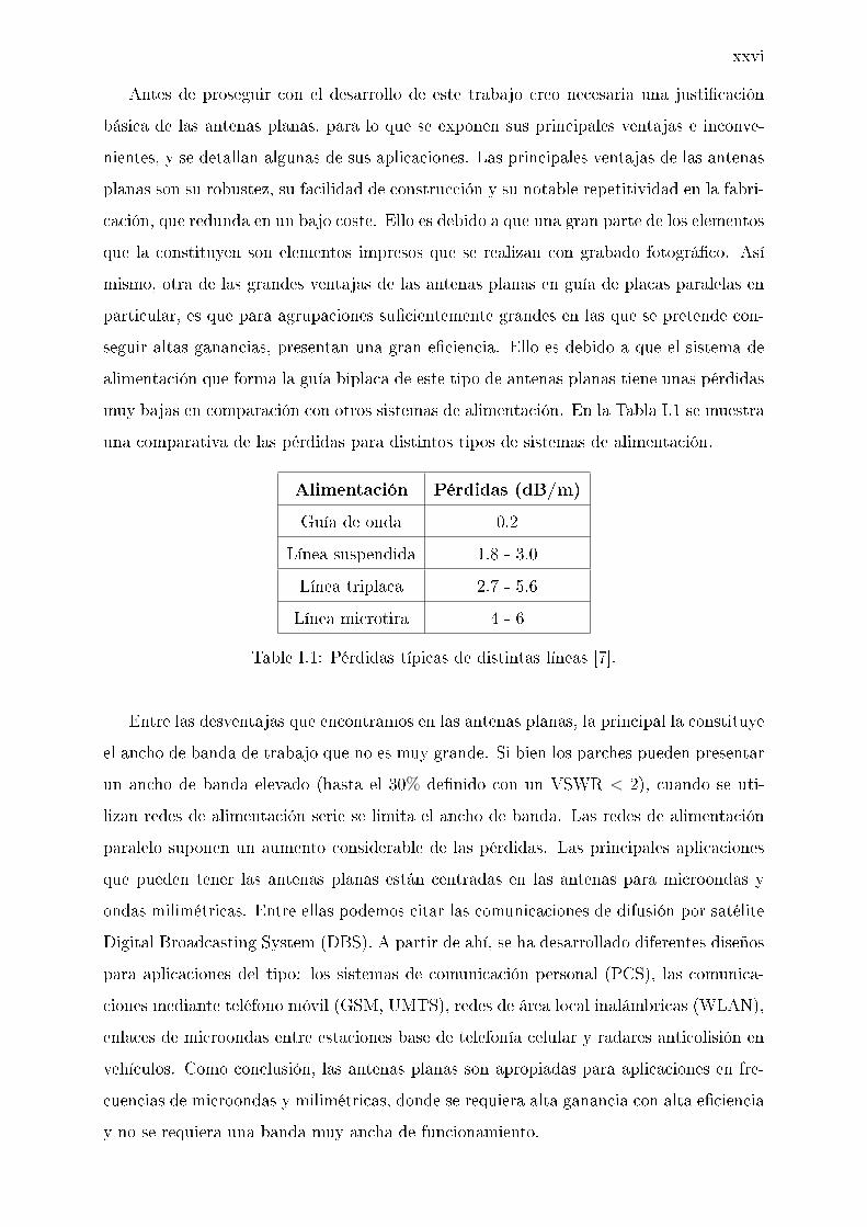
I.1 Pérdidas típicas de distintas líneas [7]. . . . . . . . . . . . . . . . . . . . . xxvi
1.1 Comparison of the typical feeding network losses . . . . . . . . . . . . . . . 9
3.1 EBG structure dimensions for 12 GHz. . . . . . . . . . . . . . . . . . . . . 44
3.2 Comparison of the directivity and the aperture eciency results for theparallel-plate slot antenna. . . . . . . . . . . . . . . . . . . . . . . . . . . . 60
3.3 EBG structure dimensions for 12.65 GHz. . . . . . . . . . . . . . . . . . . 68
4.1 Mushroom structure unit cell parameters. . . . . . . . . . . . . . . . . . . 94
4.2 Mushroom structure unit cell dimensions for εr,LH = -10.2, µr,LH = -1 (nLH
= -3.2) at 12 GHz. . . . . . . . . . . . . . . . . . . . . . . . . . . . . . . . 100
4.3 Mushroom structure unit cell dimensions with εr,LH = -2.43, µr,LH = -1(nLH = -1.56) at 12 GHz. . . . . . . . . . . . . . . . . . . . . . . . . . . . 103
4.4 Mushroom structure unit cell dimensions with εr,LH = -2.43, µr,LH = -1(nLH = 1.56) at 7.5 GHz. . . . . . . . . . . . . . . . . . . . . . . . . . . . 105
5.1 Equivalence between distributed and lumped parameters for a patch an-tenna l = λg/2. . . . . . . . . . . . . . . . . . . . . . . . . . . . . . . . . . 124
5.2 Full-wave comparisons of the performances of a square patch antenna ofxed size on a PDS, a MDS and a PMS. . . . . . . . . . . . . . . . . . . . 129
5.3 Characteristic impedance Zc of the inset fed microstrip line. . . . . . . . . 130
5.4 Complete equivalent circuit model parameters. . . . . . . . . . . . . . . . . 138
xvii

LIST OF TABLES xviii
5.5 Comparison between the microstrip patch antenna on the SIAD (measuredand full-wave simulated), on a PDS of the same eective refractive in-dex and the purely dielectric host substrate of the SIAD. The numbers inbrackets for BW and ηr represent the values computed by the approximateequations (5.8) and (5.19), respectively. . . . . . . . . . . . . . . . . . . . . 155
6.1 Dielectric thickness d = λ0/4√
(εr − 1) of the substrate for dierent dielec-tric constant εr at 8.5 GHz. . . . . . . . . . . . . . . . . . . . . . . . . . . 182

Acronyms
AD Articial Dielectric
AMC Articial Magnetic Conductor
CRLH Composite Right/Left Handed
DBS Direct Broadcasting Satellite
EBG Electromagnetic Band-Gap
EM Electromagnetic
FSS Frequency Selective Surface
HFSS High Frequency Structural Simulator
HIS High Impedance Surface
IFR Induced Field Ratio
LH Left Handed
MDS Magneto-Dielectric Substrate
MIC Microwave Integrated Circuits
MMIC Monolithic Microwave Integrated Circuits
MoM Method of Moment
MTM Metamaterial
MWS Metallic Wire Substrate
NRI Negative Refractive Index
xix

PBG Photonic Band-Gap
PCB Printed Circuit Board
PDS Purely Dielectric Substrate
PEC Perfect Electric Conductor
PMC Perfect Magnetic Conductor
PMS Purely Magnetic Substrate
RCS Radar Cross Section
RF RadioFrequency
RH Right Handed
SIAD Substrate Integrated Articial Dielectric
TE Transverse Electric
TEM Transverse Electromagnetic
TL Transmission Line
TM Transverse Magnetic
2D Two Dimensional
3D Three Dimensional
VSWR Voltage Standing Wave Ratio
VNA Vector Network Analyzer
xx

Part I
Resumen ampliado (extended abstractin Spanish)
xxi


I.1 Introducción y Objetivos
I.1.1 Motivación
Esta tesis parte fundamentalmente de la necesidad de encontrar nuevos materiales oestructuras electromagnéticas para mejorar las prestaciones de las antenas. Independien-temente de la aplicación, la continua necesidad en el área de las antenas de reducir sutamaño, de ampliar su ancho de banda, de aumentar sus características fundamentalesde radiación, de que sean fáciles de fabricar, de integrar en tecnología plana, así como subajo coste hacen que se investigue cada vez más nuevos materiales.
Las novedosas estructuras, denominadas metamateriales, son estructuras periódicasarticiales que presentan nuevas propiedades y características electromagnéticas inusualesque no se encuentran en la naturaleza. Durante los últimos años ha existido un interéscada vez mayor en el análisis y desarrollo de estos materiales. El concepto de las es-tructuras metamateriales es uno de los temas del electromagnetismo que más rápido estáavanzando y que más interés ha suscitado en los últimos tiempos. Este tema ha alcan-zado una fuerte notoriedad, hasta convertirse en una de las líneas de investigación másactivas en electromagnetismo. Las ventajosas propiedades de estas estructuras articialespermiten un amplio rango de aplicaciones en numerosos componentes y sistemas comoprincipalmente las antenas, circuitos de microondas y ltros. Estas estructuras han lla-mado considerablemente la atención en el área de las antenas en los últimos ocho años,aumentando de manera signicativa su investigación como ofreciendo nuevas aplicacionesy mejoras en sus prestaciones. Aunque por el momento estas estructuras se encuentranaún en fase de investigación, en busca de posibles aplicaciones en distintas áreas, estosmetamateriales van a desempeñar un papel fundamental en la provisión de nuevas fun-cionalidades y aplicaciones multifuncionales. A pesar del gran esfuerzo en investigaciónque se ha realizado, todavía hay un gran trabajo por realizar en el área de los metama-teriales aplicados a antenas para que estos puedan ser considerados una solución madura
xxiii

xxiv
en la mejora de las prestaciones de las antenas. Por ello se puede decir que el campode los metamateriales sigue aún en un período de investigación, desarrollo y expansióndonde se pueden realizar aportaciones novedosas, sobre todo pensando que se posee unbagaje suciente en el tema de las antenas planas para abordarlo. La experiencia endiseño, análisis y construcción de antenas planas acumulada en el Grupo de Radiaciónde la Universidad Politécnica de Madrid, así como la novedad y el interés que suscitanlos metamateriales nos va a permitir abrir un campo de posibilidades que se pretendenexplorar con esta tesis. Por lo tanto, el propósito de esta tesis doctoral es extender elconocimiento del análisis, diseño y funcionamiento de las estructuras metamateriales paracontribuir, proponer y aportar posibles soluciones que ayuden a mejorar las prestacionesde las antenas planas.
I.1.2 Objetivos
El objeto principal de esta tesis doctoral es aportar conceptos y resultados novedososen aspectos de gran interés en el ámbito de la aplicación de las novedosas estructurasmetamateriales al diseño, análisis y prototipado de antenas planas. Con el objeto demejorar las características de las antenas planas surge la idea de aplicar estas novedosasestructuras periódicas articiales para controlar, guiar y mejorar las características depropagación de ondas electromagnéticas y de radiación en este tipo de antenas.
La presente tesis doctoral se va a centrar en la aplicación de las estructuras metamate-riales para mejorar ciertas características eléctricas de tres tipos de antenas planas comoson:
Antenas planas microstrip: consisten en un par de capas conductoras dispuestasde forma paralelas y separadas por un material dieléctrico. La conguración básicaconsta del elemento radiante (parche microstrip), situado sobre un plano de masa.Ambas capas se encuentran separadas mediante el material dieléctrico, comúnmenteconocido como substrato. La alimentación de las antenas microstrip puede hacersemediante línea de transmisión microstrip, por sonda coaxial, mediante acoplo porapertura o mediante acoplo por proximidad.
Antenas planas en guía de placas paralelas: como bien indica su nombre, estánformadas por dos placas metálicas dispuestas paralelamente formando una guía deonda. En ella se genera un frente plano entre los dos conductores. La alimentación

xxv
de la guía de onda puede realizarse desde un lateral o también desde el centro.La parte fundamental la constituye la guía de placas paralelas, la cual distribuyedesde su entrada a los elementos radiantes la amplitud y fase deseada en funcióndel diagrama de radiación a sintetizar. El espacio intermedio se rellena con aire ocualquier otro material dieléctrico. Los elementos radiantes que se suelen utilizar eneste tipo de antenas son ranuras, parches microstrip o hélices. La alimentación puedehacerse mediante sondas coaxiales desde el plano de masa, mediante la utilizaciónde una red de distribución stripline conectada a un conjunto de parches excitadorescolocados en el interior de la guía o mediante ranuras excitadas por guía de ondarectangular en la cara posterior de la antena.
Reectarrays/Transmitarrays: el principio básico de funcionamiento de un re-ectarray (o transmitarray) deriva de una idea sencilla de reexión y de transmisiónde onda respectivamente, y consiste en recibir una onda electromagnética por un ali-mentador (por ejemplo una bocina) y retransmitirla. La conguración básica cons-ta de un array de elementos radiantes planos microstrip (parches, parches dobles,etc.). Cada elemento radiante de la estructura introduce un desfase necesario paraque la onda reejada (reectarray) o transmitida (transmitarray) resultante tengaunas determinadas características de frente de onda. Un reectarray se comporta demodo análogo a un reector conformado. Este tipo de antenas (reectores incluidos)utilizan soportes o mástiles de apoyo para su alimentación.
Hoy en día muchos grupos de trabajo están investigando sobre los denominados meta-materiales. Como estructuras metamateriales vamos a referirnos a los nuevos tipos demateriales periódicos construidos articialmente, que poseen propiedades electromagnéti-cas que no se encuentran normalmente en la naturaleza. Estas estructuras permitenmanipular la propagación de ondas electromagnéticas hasta un punto que no era posiblehasta ahora. Se trata de estructuras que varían de manera periódica las característicasmateriales de un medio. De esta forma es posible conseguir una característica selectivaen frecuencia para ciertos márgenes de frecuencia, así como para ciertas direcciones delespacio. Con ellas se consiguen unas propiedades electromagnéticas que son difíciles oimposibles de conseguir con materiales convencionales y cuyas dimensiones son muchomenores que la longitud de onda. Estas propiedades hacen que estas estructuras seanútiles para la construcción de diferentes dispositivos o para mejorar su comportamiento,tanto a frecuencias ópticas como de microondas y ondas milimétricas.
xxvi
Antes de proseguir con el desarrollo de este trabajo creo necesaria una justicaciónbásica de las antenas planas, para lo que se exponen sus principales ventajas e inconve-nientes, y se detallan algunas de sus aplicaciones. Las principales ventajas de las antenasplanas son su robustez, su facilidad de construcción y su notable repetitividad en la fabri-cación, que redunda en un bajo coste. Ello es debido a que una gran parte de los elementosque la constituyen son elementos impresos que se realizan con grabado fotográco. Asímismo, otra de las grandes ventajas de las antenas planas en guía de placas paralelas enparticular, es que para agrupaciones sucientemente grandes en las que se pretende con-seguir altas ganancias, presentan una gran eciencia. Ello es debido a que el sistema dealimentación que forma la guía biplaca de este tipo de antenas planas tiene unas pérdidasmuy bajas en comparación con otros sistemas de alimentación. En la Tabla I.1 se muestrauna comparativa de las pérdidas para distintos tipos de sistemas de alimentación.
Alimentación Pérdidas (dB/m)Guía de onda 0.2
Línea suspendida 1.8 - 3.0Línea triplaca 2.7 - 5.6Línea microtira 4 - 6
Table I.1: Pérdidas típicas de distintas líneas [7].
Entre las desventajas que encontramos en las antenas planas, la principal la constituyeel ancho de banda de trabajo que no es muy grande. Si bien los parches pueden presentarun ancho de banda elevado (hasta el 30% denido con un VSWR < 2), cuando se uti-lizan redes de alimentación serie se limita el ancho de banda. Las redes de alimentaciónparalelo suponen un aumento considerable de las pérdidas. Las principales aplicacionesque pueden tener las antenas planas están centradas en las antenas para microondas yondas milimétricas. Entre ellas podemos citar las comunicaciones de difusión por satéliteDigital Broadcasting System (DBS). A partir de ahí, se ha desarrollado diferentes diseñospara aplicaciones del tipo: los sistemas de comunicación personal (PCS), las comunica-ciones mediante teléfono móvil (GSM, UMTS), redes de área local inalámbricas (WLAN),enlaces de microondas entre estaciones base de telefonía celular y radares anticolisión envehículos. Como conclusión, las antenas planas son apropiadas para aplicaciones en fre-cuencias de microondas y milimétricas, donde se requiera alta ganancia con alta ecienciay no se requiera una banda muy ancha de funcionamiento.

xxvii
En la presente tesis doctoral se pretende contribuir, profundizar y realizar una impor-tante serie de aportaciones en el estudio de las potenciales aplicaciones de los metamate-riales al diseño de antenas planas en las frecuencias de microondas.
Para llevar a cabo su desarrollo se han seguido una serie de hitos que a continuaciónse enumeran remarcando las aportaciones que se han logrado con este trabajo:
1. Proponer posibles soluciones diseñando, modelando y aplicando estructuras AMC aantenas en guía de placas paralelas, tanto como sustitución de las paredes laterales,como estructura de guiado y control de la propagación de onda, con el objeto demejorar las prestaciones de estas antenas, y en particular el control de la excitaciónde las ranuras.
2. Proponer una estructura de alimentación para antenas de array de ranuras en guíade placas paralelas basada en lentes planas realizadas con metamateriales, con loque se pretende mejorar la uniformidad de la onda generada propagando un modoTEM en el interior de la guía rectangular cerrada sobredimensionada, y por lo tantolas características de radiación de estas antenas.
3. Proponer el diseño, análisis y desarrollo de un substrato magneto-dieléctrico articialpara las antenas planas microstrip con el objeto de reducir su tamaño y mejoraralguna de sus prestaciones.
4. Proponer una posible solución utilizando estructuras metamateriales para mejorar elproblema de la obstrucción y bloqueo de ondas electromagnéticas para los soporteso mástiles metálicos de apoyo en la alimentación de antenas, como los reectarrayso los reectores, con lo que se pretende mejorar sus prestaciones consiguiendo unefecto de invisibilidad de estos soportes.
Con estos objetivos se pretende que sea un trabajo de aplicaciones prácticas de losmetamateriales a las antenas planas, con varias aportaciones, tanto en la parte de análisiscomo en la parte de diseño.
I.1.3 Estructura de la tesis
Con el n de lograr los objetivos propuestos, esta tesis se organiza en siete capítulos.

xxviii
El primer capítulo realiza una introducción al ámbito de la tesis, de su motivación ypresenta los objetivos de la misma. Por último, realiza un repaso a la organización deldocumento de tesis.
El segundo capítulo introduce los principales aspectos teóricos sobre los metamaterialesutilizados en esta tesis, y ofrece un profundo estudio bibliográco del estado del arte sobreeste tema.
El tercer capítulo se centra en el análisis del efecto de estructuras AMC en antenas enguía de placas paralelas, tanto como sustitución de las paredes laterales como estructurade guiado en el interior de la guía rectangular cerrada sobredimensionada para contro-lar, guiar y mejorar las características de propagación de ondas electromagnéticas y deradiación en este tipo de antenas. Los resultados presentan el estudio de la propagaciónde onda en la guía biplaca en función de la distribución de campo y las característicasde radiación de las antenas en función de la eciencia de apertura y de la directividad.Finalmente, se analiza la viabilidad y las ventajas que ofrecen estas estructuras para estetipo de antenas en la banda de 12 GHz.
El cuarto capítulo de esta tesis propone un forma de excitación con la metodologíatradicional de generación de un modo TEM en la apertura de la guía biplaca, utilizandouna lente plana con estructura de medio zurdo que permite convertir ondas cilíndricasgeneradas por una sonda coaxial en ondas planas a la salida de la lente. Con ella se tratade reducir los efectos indeseados de rizado debido a las formas de excitación actuales delas antenas planas de placas paralelas. Se presenta el diseño, análisis y caracterización deeste método de excitación en el rango de 7.5 GHz y 12 GHz. Finalmente las ventajas einconvenientes de esta excitación son analizadas para la alimentación de las antenas deranuras.
El quinto capítulo presenta un substrato articial con propiedades magneto-dieléctricaspara las antenas planas microstrip, que permite reducir el tamaño de la antena consi-guiendo alguna mejora en sus prestaciones conservando sus características de radiación.Las propiedades fundamentales de un parche microstrip sobre un substrato magneto-dieléctrico son estudiados en este capítulo. También, se muestra el análisis y caracteri-zación de este substrato en función de sus parámetros eléctricos y magnéticos incluyendopérdidas. Además, se presenta un método para la extracción de sus parámetros constitu-tivos. Finalmente, se muestra y analiza la aplicación de un parche microstrip sobre estesubstrato en función del ancho de banda, eciencia de radiación y directividad.

xxix
El sexto capítulo analiza diferentes formas de soportes cilíndricos para intentar re-ducir la obstrucción y bloqueo de ondas electromagnéticas por estos soportes en antenas.Se presenta la caracterización y comparación de prestaciones sobre un amplio rango defrecuencia (0-20 GHz) de diferentes formas de soportes, como el diseño de estructurasmetamateriales que los recubren. También, se muestran las ventajas e inconvenientes deestos soportes cilíndricos. Las estructuras metamateriales permiten conseguir un efectode invisibilidad de estos soportes con el objeto de mejorar las prestaciones de las antenasde tipo reectarrays o reectores.
El séptimo capítulo expone las principales conclusiones alcanzadas en el desarrollo dela tesis y describe las líneas futuras de investigación que quedan abiertas.
Este resumen ampliado presenta un esquema similar al documento principal en inglés,con la salvedad de no incluir un apartado con un resumen del estado del arte de losmetamateriales (se considera más interesante consultar el propio estudio del arte expuestoen el capítulo 2). Los apartados que resumen los capítulos presentan de forma muyescueta el trabajo realizado, pero no pueden incluir todos los resultados obtenidos porrazones de brevedad. Se remite a los lectores interesados a que consulten los capítuloscorrespondientes en inglés para mayor información.
Con esta tesis se pretende que este trabajo sea un trabajo de análisis, pero sobre todode aplicaciones prácticas de los metamateriales a las antenas planas, con varias aporta-ciones tanto en la parte de análisis como en la parte de diseño. Además se abren laspuertas al diseño y análisis de otras aplicaciones, que si bien, por cuestiones fundamen-talmente de tiempo, no se han abordado en este trabajo, sí se puede decir que con lastécnicas de diseño utilizadas y los nuevos procesos de fabricación se está en disposiciónde abordarlos y de obtener resultados positivos en un corto plazo de tiempo.
I.2 Estructuras conductoras magnéticas articiales (AMC)en antenas planas de ranuras
I.2.1 Conductor magnético articial (AMC)
Un conductor magnético articial (AMC) es una estructura periódica del electromag-netismo que tiene las mismas condiciones de contorno electromagnéticas que un conductor

xxx
magnético perfecto en una banda de frecuencia especicada. Un conductor magnético per-fecto no existe en la naturaleza, pero es en cambio un modelo matemático que no soportacorrientes eléctricas de supercie (Fig. I.1).
(a) Supercie PEC. (b) Supercie PMC. (c) Supercie AMC.
Figure I.1: Diferentes condiciones de supercie.
Las condiciones de contorno de un PMC resultan de que el campo magnético tangen-cial:
−→H × n = 0 , (I.1)
Por lo tanto, en su supercie:Htan = 0 , (I.2)
Sin embargo puede presentar un campo eléctrico tangencial en su supercie:
Etan 6= 0 , (I.3)
Mientras que para un conductor magnético articial
−→H × n ≈ 0 , (I.4)
Con −→H como el campo magnético y n como vector normal a la supercie del conductor.
El PMC es el dual electromagnético o el opuesto de un conductor eléctrico perfecto(PEC), pudiendo éstos soportar corrientes eléctricas de supercie, mientras que los PMCno. Por lo tanto, la ventaja que tiene un PMC de cortar las corrientes de supercie es loque hace que este tipo de material sea ecaz para mejorar las características de circuitosde microondas y antenas.
El AMC tiene dos importantes propiedades: en primer lugar, la estructura posee unaimpedancia de supercie alta, y en segundo lugar tiene una banda de frecuencia prohibidaen la cual no se propagan ni ondas de supercie y ni corrientes.
La principal diferencia de las propiedades eléctricas entre PEC y AMC puede sercaracterizada por el coeciente de reexión para una onda plana uniforme incidente. La
xxxi
amplitud del coeciente de reexión es igual en los dos casos, y vale 1; pero la fase diereen 180. Por otra parte, la estructura conductora se comporta como un circuito abierto enel caso del AMC, mientras que el PEC se comporta como un cortocircuito. Una manerade conseguir condiciones de circuito abierto y cortocircuito son las estructuras periódicas.Los AMC muestran propiedades interesantes y están recibiendo cada vez más interés enaplicaciones para antenas. Se ha diseñado una estructura EBG 2D uniplanar basada en [8].Cada elemento de la estructura periódica es un circuito resonante inductivo L y capacitivoC paralelo equivalente, que permite cambiar la impedancia de la estructura. Cuando lasfrecuencias se acercan a la frecuencia de resonancia del circuito LC, correspondiente ala frecuencia central de la banda eliminada, la parte imaginaria de la impedancia deentrada de esta estructura es innita, indicando un comportamiento en circuito abierto.De esta manera, a las frecuencias donde la estructura periódica se comporta como uncircuito abierto conseguimos que esta estructura actúe como un AMC. Esta estructuratiene varias ventajas como son el tamaño compacto, tecnología plana, poco costo y bajaspérdidas.
En los resultados obtenidos para el diseño de la estructura AMC se presenta el coe-ciente de reexión de una onda plana uniforme incidente (normal a la supercie de laestructura). Se observa que la estructura se comporta como un AMC a 12GHz. Se presen-tan los resultados obtenidos con dos simuladores electromagnéticos commerciales: CSTMicrowave Studio que es de métodos integrales nitos en el dominio del tiempo (FiniteIntegral Time Domain(FITD)) y el High Frequency Structural Simulator (HFSS) que esde métodos de elementos nitos (Finite Element Method (FEM)). Se observa que a 12GHz la fase de una onda plana uniforme incidente del AMC es de 0. A esa frecuencia,la estructura actúa como un AMC. Para una información más detallada sobre el diseño yanálisis de la estructura AMC se puede consultar el capítulo correspondiente.
I.2.2 Análisis de paredes laterales AMC en antenas planas deranuras
Introducción
La contribución de la tesis en este apartado consiste en la aplicación de conductoresmagnéticos articiales (AMC) en las antenas planas para mejorar sus prestaciones. Porejemplo, los problemas relacionados con la no-uniformidad de la distribución de campo

xxxii
eléctrico y magnético en una guía de onda de placas paralelas con paredes conductoraseléctricas perfectas (PEC), se pueden reducir mediante el uso de paredes conductorasmagnéticas articiales. Con el objetivo de uniformizar la distribución de campo, se pre-senta el efecto de paredes AMC comparado al de las paredes PEC. Para ello, se parte deuna guía de placas paralelas en donde las paredes laterales son PEC o AMC. En contrastecon los materiales PEC, la obtención de condiciones de contorno magnéticas es una tareadifícil de conseguir porque no existen materiales convencionales apropiados que se puedanusar como AMC. Varios investigadores exponen la posibilidad de realizar un AMC de dosdimensiones. De esta manera, se consigue imponer una condición de contorno magnéticoen la guía. Estas estructuras uniplanares tienen la ventaja de ser simples, de tamañocompacto y de poderse fabricar con procesos de tecnología plana, mientras que otras es-tructuras que se comportan como AMC necesitan un tipo de proceso de fabricación máscomplicado y costoso como la de hacer vías metalizadas. Como ejemplo práctico, se apli-can estas paredes AMC a una antena plana de ranuras en guía biplaca. La uniformidadde la distribución de los campos nos va a permitir mejorar la eciencia de apertura, consi-guiendo de esta manera aumentar la directividad de estas antenas. Estas aplicaciones noshan permitido validar las ideas y los resultados obtenidos mediante simulación y medidas.
Análisis del efecto de paredes PEC y paredes PMC
Con el n de comprobar la validez de las ideas propuestas anteriormente, se realizaun análisis del efecto de paredes conductoras eléctricas perfectas (PEC) y de paredesconductoras magnéticas perfectas (PMC) ideales. En los resultados obtenidos se puedeobservar el efecto de las paredes de conductor eléctrico perfecto (PEC) y de las paredesde conductor magnético perfecto (PMC) mostrando la amplitud de la distribución decampo mediante una representación 2D. Con paredes PEC, se observa una caída muyacusada de campo en los laterales. Esto es lógico ya que ahí están colocadas las paredesmetálicas verticales. Así mismo, el campo no permanece constante en toda la apertura dela guía. Sin embargo con paredes PMC observamos que la caída de campo en los lateralesse suaviza más, lo que permite conseguir una distribución de campo más uniforme entoda la apertura. El rizado tiende a desaparecer a medida que nos alejamos de los puntosde excitación. Lo que se pretende es alcanzar una alimentación uniforme en ampltitudpara todos los elementos radiantes lo que repercute directamente en la eciencia de laantena. Así mismo aplicamos las estructuras EBG actuando como conductores magnéticos

xxxiii
articiales (AMC) en las paredes laterales de la guía biplaca. De esta manera se validanlas ideas propuestas mediante simulaciones electromagnéticas y medidas de un prototipoen guía de placas paralelas.
Resultados
En las antenas planas de ranuras se propaga un frente de onda plano quasi-TEMdentro de la estructura de placas paralelas. Con objeto de estudiar la pureza del modoTEM excitado en una guía de placas paralelas, se ha construido un prototipo en la bandade 12 GHz. Se han colocado conectores coaxiales en la placa metálica superior, conobjeto de medir la transmisión desde la entrada de la antena a cada una de las posicionesen las que se sitúan estos conectores. La guía de onda estudiada es una guía biplacarectangular de 330 mm x 318 mm con paredes laterales, entre las que se coloca un materialdieléctrico de 5 mm, en nuestro caso foam. El contorno exterior nal de la guía se terminacon un material absorbente (carga adaptada). El funcionamiento ideal de la guía sólopropaga un modo TEM (o quasi TEM). Para obtenerlo se alimenta a través de una guíarectangular convencional de ranuras en esquema resonante, la cual ejerce de alimentadory excitador del modo quasi-TEM en la guía de placas paralelas. Una característica comúna la propagación del citado modo es su degradación a medida que nos alejamos del puntode alimentación, causando una no-uniformidad en la distribución del campo. Así mismo,se han montado tres las de conectores en diferentes posiciones en la dirección transversala la propagación, con siete puntos de medida en cada una. Se ha medido el parámetroS21 de transmisión entre el conector de entrada y cada uno de los conectores de salida.
Se puede observar que en los resultados obtenidos existe una caída muy acusada decampo en los laterales de la guía. Esto es lógico ya que ahí están colocadas las pare-des metálicas verticales (PEC) que cierran toda la estructura. Es por ello, que no sepuede hablar estrictamente de un modo TEM, sino quasi-TEM. Así mismo, el campo nopermanece constante en toda la apertura de la guía. Si lo que se pretende es alcanzaruna alimentación uniforme en amplitud para todos los elementos radiantes, tendremosuna deriva importante debido a la alimentación dentro de la guía. Esto repercute di-rectamente en la eciencia de la antena. El trabajo realizado muestra la utilización deestructuras EBG actuando como conductores magnéticos articiales (AMC) en las pare-des laterales de la guía. Con la introducción de las paredes AMC, los resultados obtenidosson bastantes signicativos, consiguiendo una mejora de la uniformidad de la distribución

xxxiv
de campo en el interior de la guía biplaca cuanto más se aleja del punto de alimentación.Con ello se trata de reducir los efectos indeseados de la caída de campo en los bordes y evi-tar las reexiones de las paredes para aumentar el campo en la apertura de la guía. Estopermitirá aplicar estas paredes a las antenas de ranuras de placas paralelas consiguiendomejorar su eciencia.
La aplicación práctica de las paredes laterales AMC es la antena plana de ranuras enguía biplaca en la banda de 12 GHz con polarización lineal diseñada por Manuel Sierra-Castañer en su tesis doctoral. Dicha antena está alimentada por la guía de propagaciónestudiada en el apartado anterior. El principio básico de generación del modo TEM esel mismo. Se utilizan N elementos que actúan como excitadores de campo, actuandocomo muestreadores del mismo. Los laterales de la guía se cierran con paredes metálicasverticales. Ello produce una abrupta caída de campo en los bordes de la guía. Este hechoy el rizado del modo TEM son parámetros importantes de diseño que hacen disminuir laeciencia de este tipo de antenas. Al conseguir uniformizar la distribución de campo enel interior de la guía biplaca, la eciencia de apertura aumenta y por lo tanto mejora ladirectividad de esta antena. En los resultados obtenidos se observa que la aplicación delas paredes AMC en la guía biplaca del anterior apartado, la mejoría en la caída lateral delcampo es clara. Sin embargo, cuando las aplicamos a la antena se muestra que la mejoríaen la directividad de esta antena no es tan signicativa, debido a los efectos indeseados dereexiones de las ranuras de radiación en el interior de la guía que se mantiene en valoreselevados. No obstante, el concepto de mejorar la uniformidad de la distribución de campoen el interior de la guía biplaca, está en relación con que el acoplo con las ranuras deradiación depende de la intensidad de campo que se propaga en la guía, por lo que resultauna mejoría en las prestaciones de esta antena en directividad.
En este apartado se ha presentado el efecto de paredes AMC en vez de paredes PECen guía de onda de placas paralelas. Los resultados son bastantes signicativos, con-seguimos uniformizar la distribución de los campos cuanto más nos alejemos del punto dealimentación. Con el n de comprobar la validez de las ideas propuestas anteriormente,aplicamos estas paredes a una antena plana de ranura. Los resultados obtenidos sonconvincentes, pero se observa que aunque en la guía la mejoría con las paredes AMC esbastante clara consiguiendo una uniformidad de la distribución de campo, en la antenade ranuras el efecto de las paredes AMC es menor, debido a los efectos indeseados dereexiones de las ranuras de radiación en el interior de la guía. Para más detalle sobre

xxxv
los resultados se puede consultar el capítulo correspondiente en el documento principal.
I.2.3 Tiras AMC/PEC en guía de placas paralelas
Introducción
Un concepto de antena muy parecido a las biplaca metálicas paralelas con propagaciónpor frente de onda plano es la agrupación de guías rectangulares paralelas. De maneraprecisa estas antenas no son de placas paralelas como tal, ya que consisten realmenteen un array de guías rectangulares monomodo TE10, a las que se les añade en su capasuperior los elementos radiantes. Dichas antenas son aquellas en las que en cada uno de lospuntos de muestreo del frente plano se sitúan guías físicas que distribuyen la potencia a loselementos radiantes (guías de radiación). En este caso tendremos N guías rectangularesen las que se ha generado un modo TE10 en cada una. El modo de alimentar estasguías físicas puede ser muy parecido a los utilizados para el caso de las antenas de placasparalelas rectangulares. Sin embargo, cuando se añade un substrato para implementardichos elementos radiantes, éste se suele apoyar sobre las paredes verticales de las guías.Por ello, existe una comunicación física entre ellas que hay que resolver. Existen variasmaneras de solucionar esta problemática entre las guías físicas rectangulares. Una primeraposibilidad, es que se resuelva el problema generando las paredes verticales mediante víasmetalizadas separadas a una distancia sucientemente pequeña. El problema de dichaestructura es que es bastante complicada de fabricar, porque la posición y la distancia entrelas vías metalizadas son muy críticas. El incumplimiento de dichas distancias provocaefectos de reexiones indeseadas en el interior de las guías.
Una segunda posibilidad es la que propuso Ando et al. que consiste en la introdu-cción de una nueva forma de excitación en la guía biplaca, abandonando la metodologíatradicional de generación de un modo TEM en la apertura de la guía sustituyéndola porun modo TEN0 excitado por una guía de alimentación con N ranuras en la cara superior.Dicha guía situada en la cara inferior de la guía biplaca excita el modo apropriado que sepropagará por la guía de placas paralelas. Por lo tanto si se analiza el campo que se generadentro de la guía de placas paralelas se puede ver que el modo TEN0 puede analizarsecomo N modos TE10 adyacentes con fase opuesta. En la zona frontera entre dichosmodos adyacentes el campo eléctrico se anula. Es por ello que se genera un cortocircuito"virtual" que delimita los modos TE10 adyacentes individuales. De esta manera podemos

xxxvi
entender que la guía de placas paralelas se compone de N guías rectangulares virtualesen las que se propaga un modo TE10. Dichas guías virtuales tienen la desventaja deacoplarse entre ellas, en la zona frontera entre dichos modos adyacentes el campo eléctricodebería anularse. Por lo tanto, el cortocircuito "virtual" que delimita los modos TE10
adyacentes individuales no es perfecto y existe acoplamiento entre las guías "virtuales",lo que perjudica a la generación del campo creado dentro de la guía de propagación.
A comienzos de los años 90 se han presentado las supercies "soft" y "hard", unaterminología derivada de la acústica, con características de "STOP" y "GO" de la propa-gación de ondas electromagnéticas respectivamente, para todas las polarizaciones. Re-cientemente, varias investigaciones se han dedicado a las supercies periódicas planasutilizadas para generar nuevas condiciones de contorno equivalentes y de propiedades depropagación de estructuras de guiado de ondas. Estos estudios han estimulado variasaplicaciones en el rango de las microondas y antenas. Últimamente, algunos trabajos handemostrado que se pueden conseguir estas características de "STOP" y "GO" de ondasutilizando tiras AMC/PEC orientadas para conseguir guiar ecientemente la propagaciónde las ondas electromagnéticas. Así mismo, para acentuar la generación de condicionesde contorno equivalentes, como por ejemplo guías virtuales, lo que se propone es el usode EBG con comportamiento de conductor magnético articial, alternándose con tirasde conductor eléctrico perfecto en la placa inferior de la guía biplaca. Su nalidad es lade controlar, marcar y guiar de manera eciente el camino de propagación de las distin-tas guías virtuales en la guía biplaca y evitar efectos de acoplamiento indeseados entreellas, consiguiendo generar un cortocircuito "virtual" que delimita perfectamente los mo-dos TE10 adyacentes individuales para mejorar las prestaciones de las antenas de placasparalelas.
Resultados
El interés fundamental de utilizar tiras AMC/PEC reside en la posibilidad de imitarel funcionamiento de una guía rectangular utilizando simplemente una estructura planade este tipo, siempre que esta estructura se encuentre en una guía de placas paralelas.Las tiras de metal central (PEC) corresponderán a las caras inferior y superior de la guíarectangular equivalente, mientras que las tiras de conductor magnético articial (AMC)deberán propiciar la caída de campo eléctrico normal al plano, es decir, comportarsecomo paredes metálicas verticales. Con una sucesión de estructuras como la anterior ob-

xxxvii
tendremos una sucesión de guías virtuales, una a continuación de la otra, sin más quehaber denido un plano con sucesiones AMC/PEC. Para la comprobación de la estruc-tura descrita realizamos simulaciones con estructuras de tiras ideales (PMC/PEC) y tirasreales (AMC/PEC). Se han construido prototipos de tiras reales AMC/PEC utilizandola estructura EBG como AMC descrita en el apartado anterior. Los resultados obtenidosson bastantes convincentes en cuanto al comportamiento de propagación de la onda en lasestructuras de tiras AMC/PEC, tanto con tiras PMC ideales como con tiras AMC reales.Se observa que la distribución de campo es la de un modo TE10 en la banda de 12 GHz.Los resultados de simulación han sido validados experimentalmente. Se ha mostrado elefecto de guiado de onda, favoreciendo la propagación sobre la zona PEC e impidiéndoloen las zonas AMC. Los prototipos que se han construido mantienen las dimensiones uti-lizadas en la fase de simulación; de este modo situamos la estructura en la guía biplaca yexcitamos en el centro de la línea PEC con una sonda coaxial. Los resultados obtenidosson muy prometedores en cuanto al comportamiento de la tira AMC/PEC/AMC. Elefecto de guiado y de control de la onda en la tira PEC se conrma, y el efecto de lastiras AMC como paredes "virtuales" también. Con el n de comprobar la validez de lasideas propuestas se muestra la nalidad de estas tiras AMC/PEC/AMC, que es la demarcar claramente el camino de propagación de las distintas guías virtuales y evitar elacoplamiento entre ellas. De este modo controlamos y guiamos ecientemente la propa-gación de ondas electromagnéticas en el interior de la guía biplaca de manera que sepuedan mejorar las características de radiación de las antenas planas. Como aplicaciónpráctica se ha construido una antena plana de ranuras con estructura AMC/PEC/AMCcomo estructura de guiado. Los resultados obtenidos muestran que esta estructura esfactible en este tipo de antenas. Para más información sobre los resultados obtenidos sepuede consultar el capítulo correspondiente.
I.3 Lente plana zurda como excitación de antenas dearray de ranuras de placas paralelas
I.3.1 Introducción
La estructura básica de las antenas estudiadas en los apartados anteriores es unaguía biplaca con ranuras dispuestas en su cara superior que se excita mediante una onda
xxxviii
plana. La parte común y fundamental de todos estos tipos de antenas lo constituye la guíaonda de placas paralelas, la cual distribuye desde su entrada a los elementos radiantes laamplitud y fase deseadas en función del diagrama de radiación a sintetizar. En ella segenera un frente de onda plano entre los dos conductores. En este caso, la alimentaciónde la guía se realiza desde un lateral teniendo un único sentido de propagación. La ondaplana excita la estructura de radiación, que consiste en un array plano de ranuras enla placa superior de la guía biplaca. La red de alimentación de este tipo de antenas esuna estructura compleja, lo más fácil es realizar una excitación por acoplo mediante guíaranurada rectangular, pero el ancho de banda es reducido. Otra posibilidad es utilizarcircuitos en tecnología microstrip, pero existen dicultades de construcción y mayorespérdidas. En los dos últimos casos citados, el principio básico de generación del modoTEM es el mismo. Se utilizan N elementos que actúan como excitadores de campo. Amayor número de puntos de excitación, más uniforme será el modo TEM y menor el rizadodel campo en el interior de la guía biplaca, aunque más difícil es el diseño. En este trabajose propone una antena de ranuras sobre placas paralelas con una nueva forma de excitaciónen la guía biplaca utilizando las novedosas estructuras denominadas metamateriales.
Los metamateriales son materiales articiales electromagnéticos y multifuncionales,creados para cumplir determinados requisitos. Estas estructuras se reeren a estructurasperiódicas articiales con características inusuales, para las cuales su periodicidad es unafracción de la longitud de onda de la onda incidente. En particular, los metamaterialeszurdos llamados en inglés "left-handed" son estructuras de permitividad y permeabilidadnegativa simultáneamente, que conduce a un índice de refracción negativo. El índice derefracción de un metamaterial zurdo es negativo mientras que el índice de refracción delas partes constituyentes es siempre positivo. Estas estructuras han llamado conside-rablemente la atención en el área de las antenas y de las microondas en los últimos añosofreciendo nuevas aplicaciones. Una de las aplicaciones más común de estos metamateria-les radica en la fabricación de lentes planas. En general, la forma de las lentes ópticas esla que dene sus propiedades y, para algunas aplicaciones especícas, la forma de la lentees complicada de fabricar. La ventaja de los metamateriales para estas aplicaciones es quecon ellos se pueden fabricar lentes planas que permiten enfocar luz en áreas muy pequeñas(más pequeña que la longitud de onda de la luz). Mientras en una lente de vidrio, la formay detalles de la supercie denen sus propiedades, con un metamaterial zurdo el tamañode sus componentes dene sus características. Con el objetivo de proponer una nueva

xxxix
forma de alimentación para antenas de array de ranuras de placas paralelas y mejorarsu eciencia, se ha diseñado una lente plana zurda excitada por una sonda coaxial paraalimentar la guía de placas paralelas generando el frente de onda plano TEM.
I.3.2 Descripción
La estructura de alimentación es una lente plana zurda excitada a través de una sondacoaxial. La lente zurda intersecta con un dieléctrico convencional a través de una interfazparabólica (o parábola). La sonda coaxial se sitúa en el foco de la parábola y excita unaonda cilíndrica. La interacción entre un medio zurdo y un medio convencional con equiva-lentes densidades electromagnéticas y con interfaz parabólica, permite la transformaciónde ondas cilíndricas a ondas planas y viceversa por efecto de la refracción negativa entreel medio zurdo y el convencional. Ambos medios deben cumplir la condición de tener den-sidades electromagnéticas equivalentes. La parábola es una estructura omnipresente enaplicaciones electromagnéticas como, por ejemplo, los tradicionales reectores parabólicoscon alimentador para comunicaciones por satélite. En dichas estructuras, las ondas detransmisión y reexión se propagan siempre en la parte cóncava de la parábola. En estecaso, debido al principio de reciprocidad, la interfaz parabólica al no ser una superciede metal, permite que los rayos se refracten en lugar de que se reejen. Por lo tanto, latransformación de onda cilíndrica a onda plana ocurre de un lado a otro de la parábola. Elinterfaz parabólico se diseña mediante óptica geométrica, en particular utilizando el prin-cipio de Fermat. El gran interés del concepto de transformación de onda cilíndrica a ondaplana es, que utilizando estructuras metamateriales reales con sus parámetros ajustablesque se comporten como medio zurdo, se consiguen nuevos tipos de aplicaciones. La es-tructura real que se comporta como un medio zurdo es la estructura en forma de "seta"que ha sido inicialmente propuesta por Sievenpiper como supercie de alta impedancia,donde fue utilizada por su característica de banda de frecuencia prohibida para la supre-sión de ondas espurias de supercie en antenas planas. Dicha estructura en forma de"seta" está compuesta por array de parches microstrip conectados al plano de masa através del substrato por vías periódicas. Esta estructura en "seta" tiene la ventaja de sersimple, poco costosa y de poderse fabricar con procesos de tecnología plana incluyendovías metalizadas. Se pretende aplicar dicha estructura para la realización práctica de lalente zurda plana como forma de alimentar las antenas de ranuras de placas paralelasgenerando un frente de onda plano en el interior de la guía biplaca. Con esta forma de

xl
alimentación se trata de reducir los efectos indeseados de rizado y pérdidas, debido a lasformas de excitación actuales (N elementos que actúan como excitadores que generan laalimentación) de las antenas planas de placas paralelas.
I.3.3 Resultados
Se han realizado dos modelos de simulación que nos va a permitir diseñar la lente zurda.El primer modelo es el diseño de una lente zurda ideal, que está compuesta por materialeshomogéneos con parámetros constitutivos efectivos con interfaz parabólica entre el mediozurdo ideal y el medio diestro convencional, intercalado entre la guía de onda de placasparalelas. La estructura ha sido simulada entera con el programa comercial HFSS. Enel segundo modelo se ha diseñado una lente zurda real, conformada por la estructura enforma de seta, utilizando la información contenida en los diagramas de dispersión de lacelda unidad (en nuestro caso la estructura en forma de seta), que puede fabricarse entecnología impresa y que funciona como un medio zurdo a una frecuencia de 12 GHz. Sinembargo, como se comprueba en los resultados obtenidos en el capítulo correspondiente,construir dicha lente con la tecnología de fabricación de la que actualmente se disponeen la Universidad Politécnica de Madrid es muy complicado. El diagrama de dispersiónde la estructura en forma de "seta" muestra las bandas de frecuencias y los modos quese propagan por la estructura. Se presenta el diseño, análisis y caracterización de estemétodo de excitación en la banda de 7.5 GHz para un primer prototipo y en la bandade 12 GHz para un segundo prototipo. El objetivo de esta estructura es conseguir unaalimentación uniforme en toda la apertura de la guía. En los resultados de la simulaciónen amplitud y fase del campo generado por la lente zurda ideal, se observa una excelenteconversión de onda cilíndrica a onda plana debido a que la condición de igual densidadelectromagnética de los dos medios se cumple perfectamente utilizando un medio zurdoideal (εr zurdo = µr zurdo = -1). Dicha condición permite adaptar la interfaz entre losdos medios de manera que se eviten reexiones indeseadas y que se consiga una perfectatransformación a un frente de onda plana uniforme en amplitud y fase. Los resultadosobtenidos muestran que el funcionamiento de la lente zurda ideal propaga un frente deonda plano uniforme en el interior de la guía de ondas de placas paralelas. Además, losresultados del estudio paramétrico de la celda unidad mediante el diagrama de dispersiónpara el diseño de la lente zurda real con estructuras en forma de setas muestran unbuen funcionamiento de la estructura como medio zurdo. Sin embargo esta estructura

xli
en forma de seta tiene algunas limitaciones de fabricación en tecnología planar para sufuncionamiento en medio zurdo en el rango de 7.5 y 12 GHz que no permite realizarla porgrabado fotolitográco debido a la necesidad de un espesor de cobre de los parches muchomayor al standard de 35µm. Aunque la estructura en forma de seta como medio zurdotenga limitaciones de fabricación, los resultados obtenidos en el caso de la lente zurda idealsimulada con medios homogéneos y los diagramas de dispersión de la lente zurda real sonmuy prometedores como nueva forma de alimentación del modo TEM en estas antenas. Lautilización de estas estructuras en este tipo de antenas supone una novedad con respectoa estructuras de alimentación tradicionales. Las simulaciones del caso ideal muestranque se puede conseguir una mejoría en la uniformidad de la distribución de campo en elinterior de la guía biplaca, aumentando de esa manera la apertura de iluminación de lasranuras. La principal ventaja de utilizar esta nueva forma de excitación en la guía biplaca,siguiendo la metodología tradicional de generación de un modo TEM en la apertura dela guía, es la reducción de los efectos indeseados de rizado y pérdidas debido a la formade excitar el frente de onda plano y de conseguir mayor uniformidad en la distribuciónde campo en la apertura de la guía. De esta manera se obtienen mejores prestacionesde las antenas de placas paralelas. Para más información sobre los resultados obtenidosse puede consultar el capítulo correspondiente. Como líneas futuras a medio plazo sepretende fabricar un prototipo de lente zurda plana con estructuras en formas de seta,mediante fabricación láser para su aplicación práctica como circuito de excitación de unaantena de ranuras sobre guía de placas paralelas con polarización lineal en la banda defrecuencia de 7.5 GHz para el primer prototipo y en la banda de 12 GHz para el segundoprototipo. Se validarán los prototipos con medidas analizando la distribución de campoen el interior de la guía biplaca, la eciencia de apertura y directividad para denir lascaracterísticas de radiación de las antenas de ranuras.
I.4 Substrato articial integrado para la miniaturizaciónde antenas planas microstrip
I.4.1 Introducción
Los dieléctricos articiales son materiales que consisten en un gran numero de obs-táculos submilimétricos periódicos embebidos en un medio homogéneo, consiguiendo así
xlii
modicar los parámetros constitutivos (ε, µ) del material articial. El interés de los mate-riales articiales para aplicaciones electromagnéticas no es nuevo, si no que este tema tieneuna historia larga que data de 1898 donde Bose experimentó por primera vez un dieléctricoarticial con elementos retorcidos en esparto, que exhibían las características conocidashoy en día como características quirales. Él condujo el primer experimento de microon-das en los dieléctricos articiales. A principios del siglo XX (1920), Lindman estudió lainteracción de la onda con un conjunto de hélices metálicas embebidas en un substratohomogéneo convencional. Kock (1948) y Cohn (1949) investigaron los dieléctricos arti-ciales en lentes ligeras para antenas de microondas. Para ello insertaron esferas, discos ytiras de forma periódica, adaptando el índice de refracción ecaz del medio articial enlentes. Los materiales articiales fueron investigados teórica y experimentalmente en losaños 50 para aplicaciones de microondas. Recientemente, Sanada en 2003 ha realizado undieléctrico articial con discos resonadores alcanzando unos valores de permitividad efec-tiva εeff=2500. En 2005, Mosallaei ha estudiado dieléctricos magnéticos insertando lazosespirales en un substrato, consiguiendo aumentar los valores de ε y µ. La desventaja deeste substrato es su complicado proceso de construcción y sus dimensiones. A principiosde 2006, Machac desarrolló un dieléctrico articial con bloques rectangulares metálicosconsiguiendo aumentar el valor de la permitividad efectiva εeff a 40. Con el objetivo demejorar las prestaciones de las antenas planas microstrip se pretende diseñar, analizar yconstruir un substrato articial con propiedades magneto-dieléctricas para aplicacionesplanas. Esta estructura permite aumentar simultáneamente la permitividad y la permea-bilidad efectiva del substrato, lo que se traduce en un aumento del índice de refracción ouna reducción de la longitud de onda guiada efectiva, y por lo tanto, en una reducción delas dimensiones de estructuras planas como antenas y circuitos planos de microondas.
I.4.2 Descripción
El substrato articial (SIAD) está constituido por un mallado denso de vías metali-zadas en un substrato homogéneo convencional. Las vías metalizadas están espaciadasuna distancia mucho menor a la longitud de onda guiada para que se pueda considerarun medio homogéneo. Para caracterizar el SIAD se ha diseñado una línea de transmisiónmicrostrip de 50Ω sobre el substrato de vías metalizadas (SIAD). Para evitar un corto-circuito por contacto, existe un substrato aislador entre la línea microstrip y el SIAD.Las dimensiones escogidas para desarrollar el prototipo las imponen las dimensiones del

xliii
substrato disponible en el laboratorio y las limitaciones del láser para las vías metalizadas.Se ha utilizado el substrato RT/Duroid 6002 con una constante dieléctrica εr=2.94, unatangente de pérdidas tan δe=0.0012 a 10 GHz y un espesor de 0.508 mm. Las vías meta-lizadas con un diámetro de 0.381 mm son fabricadas por láser. La distancia entre cadavía es de 0.635 mm de centro a centro. El substrato aislador es también un RT/Duroid6002 con un espesor de 0.508 mm.
En un substrato convencional homogéneo, la propagación de la onda en el substratoes simple. El camino de la corriente se realiza directamente sin ningún obstáculo. Por elcontrario, en el substrato con vías metalizadas (SIAD), la presencia de las vías modica elcamino de propagación de la onda y, por lo tanto, el camino de la corriente eléctrica. Lasvías tienen el efecto de aumentar los valores efectivos de la permitividad y permeabilidaddel substrato debido a la presencia de éstas. Para más información sobre el funcionamientodel SIAD y el método de extracción se remite al capítulo correspondiente.
I.4.3 Resultados
Con el n de comprobar la validez de las ideas propuestas anteriormente, se ha anali-zado un modelo de simulación y circuital del funcionamiento de la línea de transmisiónmicrostrip sobre el substrato con vías metalizadas, comparando los resultados de simu-lación y de medida con la construcción de un prototipo. Con este substrato SIAD seconsiguen valores contínuos de permitividad εeff y permeabilidad µeff en función de lavariación de los parámetros del SIAD como son el diámetro de las vías metalizadas, elespesor del substrato SIAD y el espesor del substrato aislador sobre el que se imprime lalínea microstrip. Se ha mostrado que variando estos parámetros se consiguen márgenesde valores de εeff de 1.8 a 10 y de µeff de 1 a 1.9. De esta manera se consiguen variar losvalores del índice de refracción del substrato. El método utilizado para la extracción delos parámetros constitutivos del substrato con vías metalizadas, es el método del modelode línea de transmisión microstrip convencional. Para ello se han utilizado los paráme-tros S simulados y medidos de una línea microstrip de 50Ω sobre el substrato SIAD. Seha estudiado su funcionamiento mediante simulaciones que han sido experimentalmentevalidadas. Las pérdidas del substrato son comparables a las de los substratos comercialesexistentes.
El substrato con vías metalizadas (SIAD) proporciona nuevas posibilidades para el

xliv
diseño de circuitos planos sobre substratos con valores arbitrarios de permitividad y depermeabilidad. Este diseño de substrato es muy interesante, en cuanto a que puede sermuy útil para aplicaciones en sistemas cuasi-ópticos porque podemos conseguir con elSIAD varias capas con diferentes índices de refracción en el mismo substrato.
Como aplicación práctica del substrato SIAD, se diseña un parche microstrip com-parado con el correspondiente parche microstrip sobre substrato homogéneo (εr = 2.94)y sobre substrato dieléctrico con el mismo índice de refracción que el SIAD (neff = 1.99)para la frecuencia de trabajo de 1.9 GHz. La longitud de resonancia de la antena esL ∼= λg/2 = λg/(2neff ), su dimensión es considerablemente reducida por el aumento delíndice de refracción del SIAD como neff =
√εeffµeff . Se ha analizado el parche en fun-
ción de su tamaño, su ancho de banda, su eciencia de radiación y su directividad. ElSIAD permite reducir el tamaño de antenas planas microstrip consiguiendo alguna mejoraen sus prestaciones conservando sus características de radiación. Para más informaciónsobre los resultados obtenidos se puede consultar el capítulo correspondiente.
I.5 Soportes invisibles para antenas
I.5.1 Introducción y Descripción
En algunas aplicaciones, las ondas electromagnéticas radiadas por una antena sonobstruidas por estructuras mecánicas. Si la estructura es parte o está cerca de una antena,la obstrucción puede representar un bloqueo que aumenta el nivel de lóbulos secundariosy la reducción de la ganancia en las características de radiación de las antenas. Comoejemplo de las aplicaciones, el bloqueo puede ser debido a soportes o mástiles de apoyoen la alimentación de antenas de tipo reectarrays/transmitarrays o reectores. Por logeneral, en las antenas, la dirección de la onda incidente se conoce, por lo que se puedediseñar para reducir la obstrucción de una sola polarización. Este efecto de reduccióndel campo bloqueado también se denomina invisibilidad a la RF. El campo dispersoposterior de la onda incidente tradicionalmente se caracteriza en términos de un ratio decampo inducido (IFR). Es preferible caracterizar el bloqueo en términos de una anchura debloqueo equivalente Weq que es proporcional al producto de la IFR y la anchura física Wdel soporte. Mediante este término, es fácil comparar los distintos objetos con diferentesanchuras en cuanto a su invisibilidad. El ancho de bloqueo equivalente es el ancho de

xlv
una hipotética sombra de anchura que da el mismo campo disperso en la zona posterioral objeto en la dirección de la onda incidente. El menor ancho de bloqueo se obtienecuando el metal se combina para proporcionar las correctas condiciones de contorno paralas ondas en la propagación entorno a la estructura. Para objetos opacos, el bloqueo seconvierte en la anchura a alta frecuencia que equivale a la anchura física. El ancho debloqueo en la denición se convierte en un valor complejo, en donde tanto la parte real yel valor absoluto son representativos para la caracterización de la invisibilidad. La energíatotal dispersada en todos los ángulos es proporcional a la parte real de Weq. La pérdidade bloqueo debido a los soportes es proporcional a la parte real de Weq, por lo que lareducción de la directividad de las antenas también es proporcional a la parte real de laanchura de bloqueo equivalente Weq. El alto nivel de lóbulos secundarios debido a lossoportes es proporcional al valor absoluto de Weq.
I.5.2 Resultados
Se han analizado diferentes formas de soportes cilíndricos para reducir el problema dela obstrucción y bloqueo de ondas electromagnéticas. Se han comparado las prestacionesde diferentes secciones transversales de anchura física W = 54.2 mm sobre un ampliorango de frecuencia (0-20 GHz) de diferentes formas de soportes diseñadas mostrandosus ventajas e inconvenientes para la polarización TE. Este análisis nos permite denircuanto de ancho un soporte puede ser invisible a las ondas electromagnéticas. Los resul-tados obtenidos muestran que la sección transversal en forma de rombo es la que tiene elmenor ancho de bloqueo. La reducción de bloqueo de la estructura rómbica se consigueutilizando una sección transversal alargada. Esta forma nos permite conseguir una su-percie de condición "hard" para la polarización TE. Se han implementado estructurasmetamateriales con condiciones "hard" que recubran estos soportes cilíndricos para lapolarización TM. Estas estructuras han sido caracterizadas en función de sus parámetrosde diseño y se ha mostrado que permiten conseguir un efecto de invisibilidad de estossoportes mejorando así las prestaciones de antenas cuando la dirección de incidencia de laonda es conocida. Para poder denir la calidad de la invisibilidad de estos soportes se hautilizado el parámetro de anchura de bloqueo equivalente denido en el capítulo corres-pondiente. En particular, la capa del dieléctrico y las tiras metálicas han sido utilizadaspara crear la condición de supercie "hard". Los parámetros tales como el período de lastiras o la longitud de sección transversal de los soportes son críticos para conseguir un

xlvi
buen funcionamiento. Ambos factores, como el diseño de la forma y la realización de lacondición de supercie hard para los soportes son fundamentales para reducir el bloqueo.El análisis de este trabajo se ha limitado a una onda plana incidente normal y oblicua enel plano en azimut al soporte. También han sido propuestas soluciones que reducen el blo-queo simultáneamente para las polarizaciones TE y TM, consiguiendo reducir el bloqueoen una banda de frecuencia estrecha. La anchura equivalente de bloqueo es fácilmentecalculada considerando la incidencia de una onda plana en la estructura innitamentelarga, que es un problema de dispersión bidimensional. Hay que tener en cuenta que paratodos los resultados, el ángulo de incidencia de la onda es normal o oblicua en el planoen azimut. Las secciones transversales tienen un ancho normal a la dirección de propa-gación de la onda y una longitud a lo largo de ella. Los resultados han sido calculadosutilizando el software FITD (Finite Integral Time Domain) CST Microwave Studio concondiciones de contorno periódicas. Los resultados presentados permiten utilizarlos comográcas de diseño para la realización de soportes metálicos para antenas. Varias carac-terísticas importantes de las diferentes formas de sección transversal de soportes metálicosse muestran en los resultados obtenidos. Para contrastar los resultados, se van a realizara corto plazo algunas medidas de prototipos, comparándolas con los resultados numéricosobtenidos. Para más información sobre los resultados obtenidos se puede consultar elcapítulo correspondiente.
I.6 Conclusiones y Líneas futuras
Este apartado presenta las principales conclusiones derivadas del trabajo de investi-gación descrito en la tesis e incluye parte de las líneas de investigación que quedan abiertasasí como algunas ideas que pueden dar lugar a diseños futuros.
I.6.1 Conclusiones
En esta tesis, ha quedado demostrado, mediante resultados numéricos y experimen-tales, el gran potencial de algunas estructuras metamateriales en diferentes aplicacionespara la mejora de las prestaciones de las antenas planas. Durante los últimos años, haexistido un interés cada vez mayor en desarrollar estas estructuras periódicas articiales.Estudios anteriores han mostrado que hay numerosos metamateriales que permiten mejo-

xlvii
rar los funcionamientos de antenas y de circuitos de microondas. Desde entonces, se haobservado un aumento signicativo en la investigación sobre estos materiales en la co-munidad de antenas. Sin embargo, se puede decir que el campo de los metamaterialesaplicado a las antenas planas está aún en un período de investigación y de expansión,donde se pueden realizar novedosas aportaciones. En esta tesis se han analizado dife-rentes soluciones a distintos tipos de antenas, analizando las posibles ventajas prácticasde estas estructuras a diseños de antenas donde el Grupo de Radiación está trabajando.
Hemos analizado y presentado el efecto de estructuras AMC, tanto como sustitución delas paredes laterales como estructuras de guiado, dentro de la guías biplaca en la bandade 12 GHz para propagar la onda y mejorar las prestaciones de las antenas planas dearray de ranuras en guía de placas paralelas. Según la distribución de campo simuladas ymedidas en la guía biplaca, los resultados son bastantes satisfactorios. Estos dos conceptosson presentados en dos posibles aplicaciones de antenas, analizándolas y validándolasexperimentalmente. Los resultados de paredes AMC muestran que se reduce la abruptacaída de campo en los bordes de la guía, uniformizando la distribución del campo en suinterior cuanto más nos alejemos del punto de alimentación. Pero cuando lo aplicamos a lasantenas de ranuras se observa una leve mejora en las prestaciones de este tipo de antenasdebido a algunos efectos indeseados (propagación de modos superiores y por variacionespor fabricación) en el prototipo construido. Las estructuras de guiado (tiras AMC-PEC-AMC) demuestran resultados muy prometedores en términos de propagación de onda,forzando la propagación en una dirección longitudinal y cancelándola en la direccióntransversal. Los resultados de simulación y experimentales nos muestran la nalidad deestas tiras AMC/PEC/AMC, que es la de marcar claramente el camino de propagación deondas electromagnéticas de las distintas guías virtuales en la guía biplaca, evitando efectosde acoplamientos indeseados entre ellas y consiguiendo generar un cortocircuito virtual quedelimita perfectamente los modos TE10 adyacentes individuales. Hemos demostrado laviabilidad de aplicar la supercie de AMC para mejorar, controlar, y guiar la propagaciónde onda en guías biplacas. Por lo tanto, estas dos estructuras propuestas representanposibles estructuras para diseñar antenas de placas paralelas con altas prestaciones.
Siguiendo con el objetivo de mejorar las prestaciones de las antenas de ranuras deplacas paralelas, en esta tesis se ha propuesto y demostrado mediante simulación la posi-bilidad de utilizar una forma de excitación en la apertura de la guía biplaca siguiendo lametodología tradicional de generación de un frente de onda plana TEM. Este concepto de

xlviii
alimentación consiste en una lente plana con estructuras de medio zurdo excitada por unasonda coaxial, que permite convertir ondas cilíndricas generadas por la sonda en frente deondas planas a la salida de la lente. Esta forma de alimentación permite conseguir unadistribución de campo uniforme en la guía de onda sobredimensionada y reducir los efectosindeseados de rizado y pérdidas que se observan en los diferentes tipos de alimentaciónque se vienen utilizando hasta ahora en las antenas de ranuras. El diseño, el análisis yla caracterización de este método de excitación en la banda de 7.5 GHz para el primerprototipo y en la banda de 12 GHz para el segundo prototipo han sido presentados. Losresultados obtenidos han demostrado que aunque la estructura en forma de seta comomedio zurdo tenga limitaciones de fabricación, estos resultados son muy prometedorescomo forma de excitación de modo TEM para estas antenas. La utilización de estasestructuras en este tipo de antenas supone una novedad con respecto a estructuras dealimentación tradicionales.
Se ha propuesto un substrato articial (SIAD) con propiedades magneto-dieléctricaspara la miniaturización de circuitos y antenas planas microstrip. Las características fun-damentales de un parche microstrip sobre un substrato magneto-dieléctrico en términosde ancho de banda, eciencia de radiación y directividad han sido analizadas. El SIADha sido presentado como realización práctica y planar de un substrato articial capaz deaumentar simultáneamente su permitividad efectiva εeff y permeabilidad µeff , y por lotanto su índice de refracción efectivo sobre un amplio margen de frecuencia. Medianteun apropiado diseño, se ha conseguido un aumento de la permitividad y permeabilidadque produce una reducción de la longitud de onda. Se ha analizado la aplicación de unparche microstrip a 1.9 GHz sobre este substrato en función del tamaño del parche, de suancho de banda, su eciencia de radiación y su directividad. Los resultados obtenidos sonbastantes satisfactorios y muestran la viabilidad de este substrato para reducir el tamañode antenas planas microstrip, consiguiendo alguna mejora en sus prestaciones conservandosus características de radiación.
Finalmente, para reducir la obstrucción electromagnética de soportes en antenas, sehan analizado diferentes formas de soportes cilíndricos para alcanzar la invisibilidad y sehan comparado sus prestaciones sobre un amplio margen de frecuencia (0-20 GHz) paradenir cuanto un soporte puede ser de ancho y todavía ser absolutamente invisible para lapolarización TE. Se ha demostrado que se puede reducir el bloqueo utilizando supercies"hard" y formas de soportes alargadas. En este trabajo, la dirección de la onda incidente

xlix
es conocida, con lo que los soportes se han diseñado para reducir la obstrucción parauna dirección de incidencia dada. El funcionamiento para la polarización TM dependede la realización de la supercie de conductor magnético perfecto (PMC). Este últimoha sido diseñado y analizado con la realización más simple de una supercie "hard" parael caso TM: la capa dieléctrica. Esta supercie es menos sensible a la longitud de laestructura que en el caso de la polarización TE, pero el ancho de banda es más estrechoy depende del tipo de material dieléctrico usado. Las supercies articiales también sehan utilizado como capas para reducir la obstrucción causada por soportes con secciónrómbica y alargada. Se ha propuesto una posible solución que reduzca el bloqueo paralos casos de TE y de TM simultáneamente. Los resultados obtenidos han demostradouna reducción en el bloqueo en una banda de frecuencia estrecha. Esta solución se habasado en las supercies "hard" hechas de tiras metálicas sobre una capa de dieléctrico.Los parámetros tales como el período de las tiras o la longitud de sección transversal delos soportes son críticos para conseguir un buen funcionamiento. Ambos factores, como eldiseño de la forma y la realización de la condición de supercie "hard" para los soportes sonfundamentales para reducir el bloqueo. Los resultados para la polarización TM tambiénhan sido buenos pero en una banda estrecha. El ancho de banda está limitado en el casodel TM, por la capa dieléctrica. En el caso de la polarización TE tiene un ancho de bandamuy amplio en la mayoría de los casos.
Con estos objetivos cumplidos se pretende que este trabajo sea un trabajo de aplica-ciones prácticas de los metamateriales a las antenas, con varias aportaciones, tanto en laparte de análisis como en la parte de diseño. Además, se abren las puertas al diseño deotras aplicaciones, que si bien, por cuestiones fundamentalmente de tiempo, no se hanabordado en este trabajo, sí se puede decir que con las técnicas de diseño utilizadas y losnuevos procesos de fabricación se está en disposición de abordarlos y de obtener resultadospositivos en un corto plazo de tiempo.
Como conclusión general, esta tesis muestra algunas de las capacidades ofrecidaspor los metamateriales analizando, contribuyendo y proponiendo posibles soluciones quepueden ayudar a mejorar algunas de las prestaciones de las antenas planas.

l
I.6.2 Líneas futuras
A lo largo de la tesis se han ido abriendo posibles líneas de investigación para ampliarel estudio de las estructuras metamateriales y su aplicación a diferentes diseños de antenasplanas. Se enumeran a continuación algunas de las que podrían resultar interesantes:
Como alternativa a las aplicaciones de las estructuras AMC expuestas en la tesis,los resultados obtenidos en este trabajo podrían ser objeto de estudio para mejo-rar en un futuro las prestaciones de estas estructuras, analizando y optimizandonuevas supercies AMC para una amplia respuesta en frecuencia y combinar nues-tras soluciones con la solución que ha sido propuesta por la Universidad Politécnicade Valencia utilizando una supercie "hard" situadas en la cara inferior de la guía deonda sobredimensionada. La supercie "hard" permite suprimir cualquier clase depropagación, como modos de orden superiores, excepto el modo TEM. Todas estasconguraciones muestran varias posibilidades para su aplicación a antenas planasde ranuras consiguiendo altas prestaciones.
Como líneas futuras a medio plazo se pretende validar los resultados de simulaciónfabricando dos prototipos de lente plana zurda con estructuras en formas de setamediante fabricación láser para su aplicación práctica como circuito de excitaciónde una antena de ranuras sobre guía de placas paralelas con polarización lineal en labanda de frecuencia de 7.5 GHz para el primer prototipo y en la banda de frecuenciade 12 GHz para el segundo prototipo. Se validarán estos prototipos con medidasanalizando la distribución de campo en el interior de la guía biplaca, la eciencia deapertura y directividad para denir las características de radiación de la antena deranuras.
Analizar nuevas realizaciones con estructuras zurdas, como la combinación de anillosresonadores con hilos delgados para la implementación de lentes zurdas planas comonueva excitación de un modo TEM en antenas de array de ranuras en guía de placasparalelas.
El substrato articial SIAD es un candidato potencial para la realización de sistemascuasi-ópticos integrados que tienen zonas planas de diversos índices de refracciónen el mismo substrato. También, un nuevo substrato metamaterial con compor-tamiento zurdo como meta-substrato se puede desarrollar en el futuro, sin el uso

li
de líneas modeladas en el substrato homogéneo como metamaterial zurdo conven-cional. Se anticipa que el SIAD encontrará muchos usos prácticos relacionados enminiaturización y sistemas cuasi-ópticos.
Para contrastar los resultados de simulación obtenidos para reducir la obstrucciónelectromagnética de los soportes, se va a realizar a corto plazo algunas medidasde prototipos, comparándolas con los resultados numéricos obtenidos. También serealizará un análisis del efecto de una onda plana con incidencia oblicua en elevaciónal soporte, analizando la sensibilidad que tiene la anchura de bloqueo equivalentede los diferentes soportes analizados en esta tesis.
Una de las posibles soluciones futuras para reducir la obstrucción electromagnéticade los soportes para los casos de polarización TE y TM simultáneamente se podríaprever el usar estructuras en forma de seta para la polarización dual. En esta línease han comenzado a analizar estas estructuras para recubrir los soportes en [9, 10],aunque esta solución es de banda muy estrecha.


Part II
Main Document
1


Chapter 1
Introduction
During the last few years, there has been a growing interest in developing articiallyengineered structured materials, known as metamaterials. These metamaterials exhibitnovel electromagnetic properties that are not found in nature. Previous studies have re-vealed that there are numerous metamaterials able to enhance the antenna and microwavecircuit performances. As a result, a signicant increase in the research on these materialshas been observed in the antenna community. Despite the great research eort that hasbeing carried out, there are still quite an amount of investigation in the metamaterialarea that should be done before these structures in antennas can be considered a ma-ture solution to improve their performances. This thesis has been performed with theidea of contributing to some of those aspects, with special emphasis to those related withmetamaterial applications for improving planar antenna performances.
In this chapter, the main achievements of the research work contained in this disserta-tion are highlighted. A historical perspective of the works published up to now is oered.In addition, an outline of the structure of this document is given.
1.1 Motivation
This doctoral thesis parts fundamentally from the necessity to nd new materialsand structures improving the fundamental properties of antennas. Independent of theapplication, the continuing demand for small size, wide bandwidth, high eciency, easeof fabrication and integration, and low cost are always sought in antennas.
3

CHAPTER 1. INTRODUCTION 4
The metamaterials are novel articially fabricated structures and materials that havenew properties that do not occur or may not be available in nature. The unconventionalresponse functions of the metamaterials are often generated by articially fabricated in-clusions or inhomogeneities embedded in a host medium or connected a host surface.The impact of this kind of materials is enormous: if one can tailor and manipulate thewave properties, signicant decreases in the size and weight of components, devices, andsystems along with enhancements in their performances appear to be realizable.
It is known that bandwidth and radiation eciency in antennas both decrease, as sizedecreases. This is a fundamental limitation which holds irrespectively to the antennaarchitecture. Several recent studies have exposed the usefulness of metamaterial applica-tions in improving antenna performances [11,12]. These structures always raise the hopethat the fundamental limitations on antennas might be abrogated due to their exoticproperties. The use of these newly emerging class of articial materials and structures,properly engineered to improve some prescribed antenna features (bandwidth, directiv-ity, gain, eciency, front-to-back ratio, coupling, etc.) may represent a novel way ofovercoming the limitations of antennas.
In this context, an important role may be played by the metamaterials, which, dueto their electromagnetic features, have attracted a great deal of attention in recent yearsdue to their potential for several antenna applications. In this work, interest has beenfocused in particular on planar antennas. Thus, planar antennas, due to their inherentcapabilities [13, 14], are highly desirable for many systems. The use of planar technologyto develop and implement planar antennas is a very attractive solution because of the well-known advantages of this technology. Some of these advantages are low prole, potentiallow cost and easy to mount. The experience acquired with the design and analysis ofplanar antennas in the Radiation Group of Universidad Politécnica de Madrid, alongwith the newness and the interest that provoke the metamaterials allows us to open aeld of possibilities that is tried to begin to explode with this work.
Therefore, from M. Sierra Castañer's thesis [15] on the contribution in the design andanalysis of slotted arrays over parallel-plate waveguide structures, called parallel-plate slotantennas (Fig. 1.1(a) and Fig. 1.1(b)), appear some drawbacks of these planar antennadesigns as low aperture eciency results. Even that, these designs have shown highereciency than other planar antenna designs but it is seen that improvement in the aper-

CHAPTER 1. INTRODUCTION 5
ture illumination can be done. Parallel-plate slot antennas are attractive candidates forhigh-gain high-eciency due to its low transmission loss. In particular, its simple struc-ture is suitable and highly desired for mass-producible planar antennas in microwave andmillimeter wave applications. The ideal functioning of these antennas propagates a TEM(or quasi-TEM) mode. The excitation of parallel plate slot antennas have been analyzedin terms of eld distribution and aperture illumination in the parallel-plate waveguidestructures for given excitation [16]. One of the limitations of these antennas is the degra-dation of the TEM mode in the slotted oversized parallel-plate waveguide structure, whichis perturbed by its sidewalls and the coupling of slots [17]. As a consequence, the ideato apply metamaterials to improve these antenna performances may play an importantrole due to their interesting electromagnetic features. Metamaterials could be a very suit-able solution to control, guide and improve the electromagnetic waves propagation andradiation characteristics in this kind of antennas.
(a) Single beam parallel plate slot antenna [15]. (b) Double beam parallel plate slot antenna [18].
Figure 1.1: Parallel-plate slot antennas for DBS application.
Moreover, microstrip planar antennas have been analyzed and used constantly in theRadiation Group due to their low weight, low prole and easiness of fabrication. All ofthese merits make these planar antennas attractive for many antenna applications. Eventhough such antennas cannot be made arbitrarily small, since a regular patch antennaresonates at a given frequency because its dimensions is of the order of half wavelength.The interest in improving the limited characteristics of microstrip planar antennas, as theirlarger electrical size or too inherent narrow bandwidth [19,20], represents one of the mainchallenges for antenna designers. Over the years, several techniques have been proposed

CHAPTER 1. INTRODUCTION 6
in order to miniaturize the resonant dimensions of patch antennas, while maintainingtheir radiation features. In this sense, the use of lumped reactive loads, slots on the patchsurface [21], shorting pins [22], or high permittivity dielectrics may eectively reduce theresonant frequency for a xed dimension of the patch. However, the radiation pattern,the cross-polarization levels, the bandwidth and the radiation eciency may be worsenedby the presence of such elements or by the excitation of surface waves. The use of newtextured engineered materials to improve these antenna characteristics represents a novelmanner of overcoming the limitations shown by some of the well techniques for reducingthe antenna size [23, 24]. The possibility of articial material design oers new degreesof freedom for the antenna designer. Therefore, novel approaches with metamaterials forachieving patch antenna miniaturization should be explored to meet the ever increasingneed for ecient small microstrip antennas. These newly materials can be a solution todevelop eciency-bandwidth small antenna performances using design and constructiontechniques that are compatible with advanced planar technology.
Figure 1.2: Microstrip patch antenna.
In the same trend of improving antenna performances, the Radiation Group has wideexperience in designing reector antennas and measuring reectarrays. These works allowto detect that the mechanical supports for these antennas have a great inuence on theirradiation characteristics. The reduction of electromagnetic blockage in antennas is aproblem that has deserved much attention since many years ago [25]. There are manysituations where electromagnetic waves radiating from or being received by antennas areobstructed by some mechanical structures. If the structures are part of or close to anantenna, the obstruction may represent an aperture blockage causing an increase of thesidelobes and a reduction on the antenna gain. For example, the blocking structures canbe struts or masts supporting the feed in printed reectarrays, in subreectors or in feedof reector antennas. Therefore, this is why we decided to investigate the use of new

CHAPTER 1. INTRODUCTION 7
articial materials in the strut design to reduce these obstructions and blockage eectsfor such cases that the direction of the incident wave is known.
(a) Reector an-tenna [26].
(b) Reector antenna [26]. (c) Printed reectar-ray antenna [27].
(d) Printed reectarrayantenna [28].
Figure 1.3: Support struts for antennas.
1.2 Objectives
The eld of the novel articial structures denominated metamaterials in planar anten-nas is still in a period of investigation and expansion, where novel contributions can bemade. Considering that a lot of experiences in the area of planar antenna are achieved,the object of this doctoral thesis is tried to contribute to an important series of aspects inthe scope of the potential application of these structures in the design, analysis and pro-totyping in the eld of planar antennas, where the Radiation Group has wide experience.
This doctoral thesis is focused on the analysis of three types of planar antennas:
Planar microstrip antennas: consist of a pair of parallel conducting layers sep-arated by a dielectric material. The basic conguration consists of a very thin con-ducting radiating element (microstrip patch) placed above a ground plane [29]. Bothlayers are separated by the dielectric material, commonly referred as the substrate.The feeding of the microstrip antennas can be done by microstrip transmission line,by coaxial probe, by aperture coupling or by proximity coupling [30].
Parallel-plate slot antennas: as indicates its name, they are formed by twoparallel-plate shorted with physical metallic walls at the width forming a waveguide.A plane wave is excited inside the parallel plate waveguide [15]. The feeding of thewaveguide can also be made from a lateral or from the center of the oversizedwaveguide. The fundamental part that constitutes this kind of antennas is the

CHAPTER 1. INTRODUCTION 8
parallel-plate waveguide structure, which distributes to the radiating elements thewished amplitude and phase based on the radiation pattern to synthesize. Thespace between these two-plate waveguide is lled up with air or any other dielectricmaterial. The radiating elements that usually are used in this type of antennas areslots, microstrip patches or helixes. The feeding structure can be done by a coaxialprobe [31], by a excitation circuit of patch arrays in microstrip planar technology [18]or by a slot feed waveguide [32].
Printed reectarrays/transmitarrays antennas: the basic operation principleof reectarrays (or transmitarrays) derives from the reection or transmission waverespectively, and consists of receiving an electromagnetic wave from a feed (forexample a horn) and resend it. The basic conguration consists of planar microstrippatch arrays (single patch, double stacked patch, etc.) illuminated by a feeder. Thereected (reectarrays) or transmitted (transmitarrays) phase by each element ofthe arrays will be adjusted to generate a planar front phase characteristics. Thisphase can be controlled with the use of stubs of variable length, or changing theresonant dimension of each patch [27, 33]. The reectarrays behave like reectorantennas. This kind of antennas (reectors including) use struts or masts thatsupport the feed.
Nowadays many research groups are investigating on the denominated metamaterials.Metamaterials structures are broadly dened as the new types of articially constructedmaterials with unusual electromagnetic properties that are not readily available in thenature. These structures allow to manipulate the electromagnetic wave propagation.They vary in a periodic way the material characteristics of the constituent homogeneousmaterials with properties that achieve a selective characteristic in dierent frequencyrange as for dierent directions. These properties cause that these structures are usefulfor the construction of dierent devices or for improving its behavior, as much at optical,microwave and millimeter waves frequency.
Before continuing with the development of this work, we believe necessary a basicjustication of the planar antennas, for which their main advantages and disadvantages areexposed, and some of their applications are detailed. The main advantages of the planarantennas are their robustness, its facility of construction and its remarkable repetitive inthe manufacture, that results in a low cost. Also, other advantages of the planar antennas

CHAPTER 1. INTRODUCTION 9
in parallel-plate waveguide structure for large arrays are the higher gain and eciency.This is because the feeding network, that forms this type of planar antennas, has very lowlosses in comparison with other systems of feeding. In the following table is a comparativelosses for dierent types of feeding networks at 12 GHz [7].
Feeding network Losses (dB/m)Waveguide 0.2
Suspended line 1.8 - 3.0Stripline 2.7 - 5.6
Microstrip line 4 - 6
Table 1.1: Comparison of the typical feeding network losses
The main disadvantage, that is found in the planar antennas, is that the bandwidthis not so wide. Although the patches can present a high bandwidth (until 30% with aVSWR < 2), the bandwidth is limited when series feeding networks are used [34]. Theparallel feed networks suppose a considerable increase of the losses.
The main applications that can have the planar antennas are centered in the an-tennas for microwaves and millimeter waves. Among them, it can be mentioned theTV communications by satellite Digital Broadcasting System (DBS), area in which dif-ferent investigation groups have published dierent designs [35, 36]. From there, it hasbeen developed dierent designs for applications as the personal communication systems(PCS), the mobile communication systems (GSM, UMTS) [37], wireless local area net-works (WLAN) [38], collision warning radars in vehicles [39]. Planar antennas are appro-priate for applications in microwaves and millimeter frequencies, where is required highgain with high eciency.
As a result, this thesis may help to a better understanding of the capabilities oeredby metamaterials to improve these antenna characteristics. An engineering approach isadopted with systematic emphasis on developing practical applications, improving an-tenna features in terms of performances and functionalities.
After a previous revision work of current state of the art and general vision of meta-material applications in planar antennas, four main topics of work have been dened, sothat the main objectives of the thesis are wrapped around them. These main objectives,as well as a brief explanation of the proposed methods to full them and its contributions,

CHAPTER 1. INTRODUCTION 10
are summarized as follows:
Objective 1: this thesis will analyze the electromagnetic waves propagation in terms ofeld distribution in the parallel-plate waveguide structures for a given excitationand the radiation characteristics in terms of aperture eciency and radiation direc-tivity in parallel-plate planar antennas. Moreover, it will propose possible solutionsusing metamaterials as articial magnetic conductors (AMC) with the purpose toimprove their wave propagation and radiation characteristics. In order to achievethis objective, AMC surfaces have been applied and analyzed placed as sidewallsinstead of the conventional metallic walls or as propagation strips in the oversizedparallel-plate waveguide with the purpose to enhance, control and guide ecientlythe wave propagation in theses kind of waveguides. Practical applications of theseAMC structures to parallel plate slot antennas in the 12 GHz band will be presentedand analyzed in terms of aperture eciency and radiation directivity.
Objective 2: this thesis will propose and analyze a feeding concept for TEM wave exci-tation in parallel plate slot antennas, with the purpose to enhance the uniform elddistribution inside the parallel-plate waveguide structure, as well as to improve theaperture eld illumination of the radiating elements. In order to accomplish thisobjective, a planar left-handed (LH) metamaterial lens excited via a coaxial probewill be designed, analyzed, fabricated and measured as a way to feed parallel-plateslot antennas with an attractive due to its advantage of being simple and can befabricated using planar process technology. Radiation characteristics of a parallel-plate slot antenna with this feeding network will be presented and analyzed in termsof aperture eciency and directivity.
Objective 3: this thesis will develop and propose a new substrate with magneto-dielectricproperties with the purpose to miniaturize planar microstrip circuits and patch an-tennas, as well as to achieve good propagation and radiation characteristics, respec-tively. Moreover, it will analyze and discuss the fundamental properties of patchantennas on these kinds of substrates in terms of bandwidth, radiation eciencyand directivity. In order to full this objective, an articial dielectric substrate asa practical realization of a magneto-dielectric substrate will be designed, fabricatedand characterized focusing on their eective constitutive parameters. A practicalapplication of a patch antenna on this substrate will be presented and analyzed in

CHAPTER 1. INTRODUCTION 11
terms of size, bandwidth, radiation eciency and directivity.
Objective 4: this thesis will examine how to improve the problem of reducing blockagecaused by metal struts in antennas, as reectarrays or reectors, with the purposeto achieve invisibility, as well as to have good performances in terms of sidelobesand gain of these antennas. Moreover, it will study dierent oblong cross-sectionalshapes of metal cylinders and it will analyze which are the most interesting cross-section to be considered to reduce the blockage for a given direction of incidence.In order to carry out this objective, an analysis of blocking objects, that havewidth comparable to the wavelength, with emphasis on ideally hard cylinders isdone and compared. The drawbacks and advantages of each one are highlighted.Also, possible solutions using hard surfaces on the strut design, to reduce theseobstructions and blockage eects for such cases where the direction of the incidentwave is known, are investigated. Both factors, shape and realization of the hardsurface for the struts are fundamental to reduce blockage.
With these objectives, the general purpose of this work is to be a practical application ofthe metamaterials to planar antennas, with several contributions, as much in the analysispart as in the design part.
Therefore, this doctoral thesis allows to extend the knowledge of the analysis, designand operation of metamaterial structures to contribute and propose possible solutionsthat help to improve the planar antenna performances using these novel structures.
As observed from the description of the main objectives of the thesis, we may noticethat a similar methodology is followed in the four areas in order to accomplish eachof the objectives. First of all, a thorough study of the state of the art in the topic ofinterest is given, in order to know the situation of research in the area of metamaterialsto be covered. Afterwards, theoretical studies are done in order to propose a solutionusing metamaterial structures to be fabricated and measured so that the advantages ordrawbacks of these structures are pointed out. Real prototypes and measurements arecarried out to validate the simulated results. These are key aspect in this thesis, sincewe aim to apply metamaterial structures in practical antenna applications. Finally, theanalysis of the results is done, and the main conclusions for each of the four areas of studyare given.

CHAPTER 1. INTRODUCTION 12
1.3 Outline of the Thesis
The main document is organized in seven chapters. Chapter 1, already exposed,presents the motivation that purpose this work. Furthermore, the main objectives arehighlighted and an outline of the thesis is detailed.
Chapter 2 introduces the metamaterial structures. A thorough revision of the state ofthe art in metamaterials, detailing a classication of them and its applications, are carriedout. The main theoretical aspects of the three kinds of metamaterials (articial magneticconductor (AMC), left-handed (LH) material and articial dielectric (AD)) that are usedin this thesis are dened.
Chapter 3 studies the eect of AMC surfaces placed as sidewalls or as propagationstrips in the parallel-plate waveguide structure of a parallel plate slot antenna. The wavepropagation in terms of eld distribution and the radiation characteristics in terms aper-ture eciency and directivity is analyzed. The benets and drawbacks of these structuresin parallel-plate slot antennas are discussed. Two practical planar antenna applicationsare presented in the frequency range of 12 GHz.
Chapter 4 proposes a feeding, based in a planar left-handed lens, for plane TEM waveexcitation in parallel-plate slot antennas. The design, analysis and characterization arepresented. Also, the advantages and drawbacks of this feed are analyzed in terms of elddistribution inside the oversized waveguide structure and in terms of aperture eciencyand directivity for the practical planar slotted antenna application in the frequency bandof 7.5 GHz and 12 GHz. A comparison with conventional TEM wave excitations isdiscussed.
Chapter 5 presents a novel substrate integrated articial dielectric (SIAD) as a prac-tical planar realization of a magneto-dielectric substrate. The fundamental properties ofa patch antenna on a magneto-dielectric substrate in terms of their radiation character-istics are discussed. A SIAD microstrip line is analyzed and characterized in terms of itseective constitutive parameters including electric and magnetic losses. A practical SIADpatch antenna is demonstrated and discussed in terms of bandwidth, radiation eciencyand directivity.
Chapter 6 analyzes dierent oblong cross-sectional shapes of metal cylinders to reduce

CHAPTER 1. INTRODUCTION 13
the obstructions and the blockage eects of struts in antennas. These struts are char-acterized and compared performances in terms of equivalent blockage width over a largefrequency band (0-20 GHz) to nd out how thick a strut can be and still be quite invisiblein dual (TE and TM) polarization. Also, hard surfaces on the strut design are studied.The drawbacks and advantages of each one are presented and discussed.
Finally, chapter 7 summarizes the results and concluding remarks, and proposes somefuture research topics.
The most important results and contributions to the state of the art that were ob-tained along the work of these thesis have been presented and accepted for publication inleading international technical journals, and many conference papers have been presentedat the most important international and national conferences in the elds of antenna andmetamaterials. Finally, three Master Thesis have been supervised by the author of thisthesis within this work's scope. All the details of the contributions of this thesis are givenin chapter 7.


Chapter 2
Metamaterials
The purpose of this chapter is twofold. Firstly, a look at metamaterials in electromag-netics from a general point of view, a tentative denition, an overview of the dierentclasses of metamaterials and the main concepts related with these materials are given,with special emphasis on the aspects that will be addressed along the thesis. As a sec-ond intention of this chapter, previous work on both metamaterials and these structuresin planar antennas is detailed, obtained after an extensive search eort in the existingliterature. The general theoretical background required to understand the rest of thisdocument is presented. The aim is to give the reader an idea of the state of the art aswell as to point out the main open topics of current interest, which have motivated thework of this thesis.
This chapter has been divided into two parts. We refer to the rst part as an overviewof these structures with a tentative classication and application of them, and the secondpart refers to those metamaterials used in this work. The dierent metamaterials used inthis thesis are claried below.
2.1 Denition
Since their discovery, interest in metamaterials has grown explosively. Eight years havepassed since the emergence of the metamaterials have proved to be exceptionally promisingfor both research and applications. Accordingly, the number of related publications peryear has risen from a few in 2000 to some several hundreds in 2008, and continues to grow.
15

CHAPTER 2. METAMATERIALS 16
Every year has brought some new results or ideas, promising useful devices for the future.A number of detailed review and books have been published recently [4,11,12,4043]. Theinvestigation of metamaterials is currently one of the most active topics in engineering andphysics. There are considered as one of the emerging technologies that have the potentialto signicantly change everyday life in the near future.
The understanding of materials is quite old and has been studied by researchers forcenturies. In the literature, various physical properties of a material under many dierentparameters are exposed. In Fig. 2.1 is shown a tetrahedron that is the classical schemeused to describe the main aspects of the materials [44]. The principal aspects that shouldbe considered in the study of materials are the relationship among processing, structure,properties and performance of them.
Figure 2.1: Tetrahedron of the basic elements of the materials in the eld of science andengineering.
Moreover, in many cases the properties of materials, that determine how the materi-als will interact with electromagnetic radiation, may be surprisingly diering from thoseof the constituents. But, it is known that the inner structure of a material contains somany degrees of freedom. The characterization of a material gives a large amount ofinformation that is essential as known in many eld of science and engineering. Rapidlygrowing demand of electromagnetic materials with various exotic properties is precondi-tioned by continuous development of novel technologies. Electromagnetic properties ofnaturally available media are restricted by physical reasons, that is why strong progress
CHAPTER 2. METAMATERIALS 17
in studies of articial materials is observed during last years. These complex materials al-low us to achieve extraordinary electromagnetic properties which are sometimes even notavailable in natural materials. The name for articial complex materials that agree withthis characteristic of unconventional properties can be called metamaterials. The word"metamaterial" emerged into the research and literature of electromagnetics in the earlyyears of the present century. The term was coined in 1999 by R. M. Walser of the Uni-versity of Texas at Austin [45]. He dened metamaterials as a "macroscopic compositeshaving man-made, three-dimensional, periodic cellular architecture designed to producean optimized combination, not available in nature, of two or more responses to specicexcitation". Another denitions of the present time for metamaterials are the one giveby [41]: a metamaterial is an articial structure or material that, in a certain frequencyrange presents unusual electromagnetic properties (as propagation of backward waves,negative refraction, presence of forbidden zones,...), which gains its properties from itsstructure rather than directly from its composition. To distinguish metamaterials fromother composite materials, the metamaterial label is usually used for a material which hasunusual properties. It is obvious that in the above-cited denitions, the metamaterialsare dened in a general concept. However, the denition for the metamaterials shouldcontain something more fundamental. Metamaterials are hard to dene and classify. Aunique denition for metamaterial does not exist within the research community and inthe literature. Electromagnetics of complex materials is a eld where researchers mayhave their background in dierent areas that are reected in the existence of dierent def-initions for the term "metamaterial". It should be clear from the above that the conceptshave emerged from dierent backgrounds and, as a result, the terminology is non-uniformand sometimes confusing, making it dicult to understand how the dierent surfaceswork and how they can be applied. Therefore, in order to help clarify the situation, aglobal denition for metamaterials that might satisfy most researchers in the eld of elec-tromagnetic materials would probably be that those materials are simply something elsethan conventional materials. The prex "meta" means after, beyond and also of a higherclass. For that reason, in a more specic vision, metamaterials can be dened as articialengineered complex electromagnetic functional structured materials, by placing them ina periodic manner, have superior (electromagnetic) material properties that can not beobserved in the constituent materials used to manufacture them. Moreover, they possessproperties that are not observed in nature. Obviously, it refers with metamaterials toman-made materials that are purposely designed and engineered to do a certain function

CHAPTER 2. METAMATERIALS 18
because nature does not oer materials for free which would fulll these requirements.These properties can not be determined by only material components, shape and con-centration of the constituents inclusions, but rather these are new properties emergingdue to specic interactions with electromagnetic elds. In other words, a metamaterial isthe co-existence of materials with well-dened properties that causes new properties dueto it composition. Since often metamaterials are composed of structures or man-madescatterers, that are very strongly reacting and therefore dominantly responsible for thebehavior, the global metamaterial properties depend of the physical dimensions of thesescatterers and their periodicity. Metamaterials are articial periodic structures with lat-tice constants that could be much smaller, in the order or larger than the wavelength ofthe incident electromagnetic radiation. The metamaterials is a breakthrough mainly dueto their ability to guide and control eciently electromagnetic waves and the materialproperties. In recent years, a lot of research have been done around the world, especiallyin electromagnetics, with the purpose to study, develop and design metamaterials andtheir applications. In the way to justify the specic terminology used here for the meta-materials as articial engineered complex electromagnetic functional structuredmaterials, some comments about the use of these terms are made. The term articialmaterial means that it does not exist in nature. The term engineered material impliesnon-natural materials, so man-made material, where it can be tailored to display desiredproperties. The term complex electromagnetic material denes that the material is madeup composed of distinct components in the electromagnetism and implies the possibility todescribe the material in terms of equivalent homogeneous permeability and permittivity.With the term functional material, the emphasis is shifted from the internal descriptionof the material to the application. Materials are designed through technological processesin order to fulll a certain function. The term structured materials is common in the eldof construction materials and there the emphasis is naturally on strength and mechanicalproperties. By clever combination of existing materials it is possible to achieve greatimprovements in various mechanical properties.
2.2 Classication
The great activity of present research on metamaterials in electromagnetics is produc-ing a large amount of investigations, and the rate is probably only increasing. There are a

CHAPTER 2. METAMATERIALS 19
lot of classication for metamaterial structures as the ones proposed by Rhamat-Samii etal. in [46] or Caloz et al. in [11] or Engheta et al. in [12], but here we preferred to extendthese classication including some other articial materials. A tentative classicationof the present existence classes of metamaterials is presented. The concept of metama-terials is treated quite general among the researchers and encompasses a broad rangeof modern topics such as frequency selective surfaces (FSS), electromagnetic/photonicbandgap (EBG/PBG) structures, left-handed (LH) materials, articial magnetic conduc-tors (AMC) or high-impedance surfaces (HIS) or hard/soft surfaces, articial dielectrics(AD), and plasmonic medias. Several dierent classes of articial materials which are con-sidered as metamaterials are identied and their particular characteristics are discussed.In Fig. 2.2, a chart gives a tentative classication of the dierent kind of existing meta-materials.
Figure 2.2: Classication of metamaterials.
Frequency selective surfaces (FSS) are dielectric layers of very large extent, whichcontain planar conductive elements on its true side and which backside is free (withoutany metallic part). Planar conductive elements can be arbitrarily shaped, but within one
CHAPTER 2. METAMATERIALS 20
selective surface, all the elements are usually identical. Metallic elements can be con-ductive (electrically conductive elements) or can be implemented as slots in continuousmetallic true side (magnetically conductive elements). If the true side of the selective sur-face is illuminated by harmonic waves of various frequencies, some waves are transmittedwith a minimum attenuation, some waves are totally reected back to the half-space ofthe source, and some waves are partially transmitted and partially reected. Hence, thesurface performs a frequency selection of incident waves. So, a FSS can be viewed as alter for plane waves at any angle of incidence [47].
Electromagnetic/photonic bandgap (EBG/PBG) materials are also known asphotonic crystals. They are periodic structures that can be made by metallic, dielectricor metallodielectric elements. Their function is to aect the propagation of electromag-netic (EM) waves. These structures are used to control and manipulate the propagationof electromagnetic waves. The EBG structures have two important attributes that areproducing a bandgap and localized frequency window in the bandgap by breaking theperiodicity of the structure. The rst property is useful in using EBG as a spatial and fre-quency lter, while the second property is useful in propagating the EM wave in a desiredfrequency and direction. There exist 1D, 2D or 3D periodic structures in which the prop-agation of electromagnetic waves is inhibited in some frequency bands (called bandgapsor stopbands) or directions that are determined by the periodicity of the materials andtheir dielectric constants.
Articial magnetic conductors (AMC) (or high impedance surfaces (HIS)) havenew emerged properties as a magnetic response, even if the component materials arenon-magnetic. These materials react to external elds mostly by their surfaces. We canassociate the hard and soft surfaces in the class of the AMC because their behavior usedarticial magnetic conductors (AMC) and perfect electric conductors (PEC).
Left-handed (LH) materials have been called by many names as negative refractiveindex (NRI) material, negative-index material (NIM), double-negative (DNG) metama-terial, backward wave media, negative phase velocity (NPV), Veselago media. Thesematerials are the most famous metamaterials. These properties have simultaneously neg-ative permittivity and permeability. Composite right/left-handed (CRLH) concept is anarticial transmission line (TL) approach that describe the behavior (RH or LH) of thesemedium depending on the frequency range of working. These medias can be included in

CHAPTER 2. METAMATERIALS 21
this left-handed class of metamaterials.
Articial Dielectrics (AD) consist of a large number of subwavelength conductingobstacles embedded in a homogeneous host medium [48]. Calling such dielectrics asmetamaterials make sense because the conducting properties of metals are being changedto a dielectric-type behavior in the macroscopic properties. One of the kind of AD canbe the magnetic materials (mu negative (MNG) media). Chiral medias are also includedin this class.
Plasmonic medias (or epsilon negative (ENG) media) is the name given (in 2000)to a discipline seeking to benet from the resonant interaction obtained under certainconditions between an electromagnetic radiation and the free electrons with the interfacebetween a metal and a dielectric material. This interaction generates density waves ofelectrons, behaving like waves and called plasmons or surface plasmons at optical frequen-cies. Conventional surface plasmons occur at the interface between two dielectrics mediacoated by a thin layer of metal; they couple to the evanescent wave due to total internalreection at the specic incidence angle corresponding to the plasmon resonance [49].The plasmons in metamaterials are very dierent because they appear in two media ofsame density and do not require a metal collector, using the plasmonic nature of the LHstructure instead of that metal. It was shown that one can obtain the same plasmonfrequency that the incident light but with a shorter wavelength. This phenomenon shouldallow the realization of conductors much smaller than optical ber (because the diameterof the conductor is proportional to the wavelength) but propagating an important ow ofinformation (thus higher than an electric conductor). The plasmonic medias have manypotential applications. For example, by controlling the behavior of light, it could im-prove the resolution of the microscopes or increase the eciency of the electroluminescentdiodes. In electronics, it could lead to eective devices for couplings between optic andelectric signals.
2.3 Applications
The main potential applications of the metamaterials interesting for us are focusedon antennas in the microwave frequency range [50]. Few practical applications of thesematerials in this area exist because these structures are still in a stage of investigation

CHAPTER 2. METAMATERIALS 22
presenting the theoretical concepts, their properties and developing new types of articialstructures that will give rise to new microwaves, millimeter and optical band applica-tions. From year 1997, the main line of interest of works of practical applications thatthey are published is the study, analysis and application of the metamaterial structuresin the scope of microwave and millimeter applications. Several researchers are the mainpioneers in practical applications of these materials to antennas. These novel structuresbrought to electromagnetism new concepts and new solutions to solve dierent problems.Apart from antenna applications, metamaterials have many others applications. In orderto drive this technology towards the market place it is needed to identify component fea-ture of metamaterial structures that give added value over and above current approaches.Cooperation with industry is essential in order to identify the needed requirements andto promote the use of this innovative and promising technology in real world applications.The advantageous properties that present these articial structures mainly allow a widerange of applications in numerous components and systems like the microwave circuits, l-ters, miniaturization, controlling wave propagation, tuneable materials, imaging systemsand THz applications. They show promises for a variety of microwave applications suchas new types of beam steerers, band-pass lters, lenses, microwave couplers, antennas. InFig. 2.3, some of the potential applications of the metamaterials are highlighted [11,12,46].
Figure 2.3: Applications of metamaterials.
The above scheme gives a small insight into the large potential industrial applicationof the metamaterials. An exhaustive review of applications is beyond the scope of thisshort overview. The applications at microwave and millimeter waves are clearly centeredaround the communication system where components like cellular phones will have to be

CHAPTER 2. METAMATERIALS 23
more exible and agile in the future or for low-cost steerable antenna applications. In thecontext of tuneable materials for communications, intense eort is also dedicated to arti-cial materials for radiofrequency (RF) and microwaves form which attractive industrialapplications are expected. Several telecommunication companies are dedicating researcheort to this regard. The amplication of the response of a constituent or inclusion in ametamaterial is also highly interesting for sensing applications, i.e. for biochips to enhancesensitivity. Also, exible electromagnetic wave propagation control enabled by EBG, FSSand other metamaterials is an excellent opportunity to optimize the radiation character-istics of light emitting diodes to couple the light generated in the high refractive indexmaterials out into air eectively. Opposite eort is related to lasers, where metamaterialsare used to lower the treshold of lasers. All microwave and millimeter wave componentsrequire waveguiding structures, and planar circuit and waveguide miniaturization; thiscan be done using metamaterials in particular EBG materials. Finally, metamaterialapplications allow to optimize the radiation characteristics of individual antennas, andto optimize and decouple more eectively antenna arrays for steerable antenna array orsensing and imaging systems for biomedical applications. This has wide benets for com-munication technologies, microwave and millimeter wave imaging applications in medicineand security, and many other areas.
2.4 Metamaterials used in this Thesis
In this section an historical review in the design and analysis of the extensive family ofmetamaterials used in this thesis, with their main properties, is presented. It is completedwith previous work in the application of metamaterials to antennas, obtained after anextensive search eort in the existing literature. The aim is to give the reader an ideaof the state of the art as well as to point out the topics of current interest, which havemotivated the work of this thesis.
2.4.1 Electromagnetic BandGap Materials
The electron has been the main axis of the technological revolution during XX century.From the appearance of the lasers, the photon (the light particle) disputes the hegemonywith electrons. In the theoretical aspect, the similarities in electron-photon behavior are

CHAPTER 2. METAMATERIALS 24
known from the birth of the quantum physics in 1920. In addition, a great mathematicalsimilarity between the equations of Maxwell, that describe the ondulatory behavior ofelectrons, and the equation of Schrödinger exists, that describes the one of photons.
Great part of the discoveries in physics in the past century is due to the study of thewaves in periodic structures, like for example x-rays, the electron diraction in crystals, theband structure of electrons, etc. These advances have a repercussion in the technology ofnew materials with unusual behaviors. Due to this similarity of behavior between electronand photon, within the last decades there has been a breakthrough in the control of theoptical properties of materials opening the path to control the emission and propagationof light. If it were possible to design and make materials that prohibited the propagationof the light, or they allowed it, in determined directions for certain frequency range, thepresent technology would take a great step towards a new revolution, although now opticalinstead of electronics.
The discovery of electromagnetic bandgap (EBG), in the latest 1980s, restarted theresearch on the periodic structures. In the last years the eld of periodic structures forelectromagnetic waves has received an important impulse in physics and engineering withthe introduction of these novel concepts. These novel concepts were originally developedby Yablonovitch [51] and John [52] in the optical wavelength region. The idea was toapply 3D articial periodic structures that present forbidden zones of propagation in theinhibition of radiation by spontaneous emission of light in laser sources and semiconduc-tors. Previously, Brillouin studied the behavior of the electromagnetic waves propagationin periodic structures and observes that these have discontinuities in points or regionsthat are related with their dispersions [53, 54].
Attention has increased in the design of periodic structures that control the propaga-tion characteristics or the boundary conditions of electromagnetic elds in a desirable way.Such structures have been referred to as electromagnetic bandgap structures as knownin microwave and antenna domains. The EBG materials, also called photonic bandgap(PBG) or photonic crystals in the optical area due to their analogy to semiconductorcrystals where electron bandgaps can be found. The EBG materials involve distancesthat are on the order of half wavelength or more and are described by other periodicmedia concepts. These materials are dened as 1D, 2D or 3D periodic structures thatprevent the propagation of the electromagnetic waves in a specied band of frequency
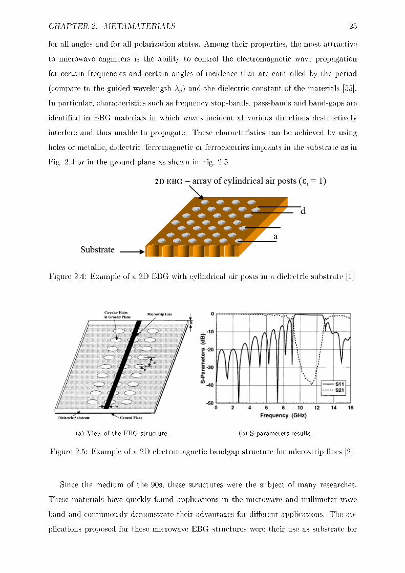
CHAPTER 2. METAMATERIALS 25
for all angles and for all polarization states. Among their properties, the most attractiveto microwave engineers is the ability to control the electromagnetic wave propagationfor certain frequencies and certain angles of incidence that are controlled by the period(compare to the guided wavelength λg) and the dielectric constant of the materials [55].In particular, characteristics such as frequency stop-bands, pass-bands and band-gaps areidentied in EBG materials in which waves incident at various directions destructivelyinterfere and thus unable to propagate. These characteristics can be achieved by usingholes or metallic, dielectric, ferromagnetic or ferroelectrics implants in the substrate as inFig. 2.4 or in the ground plane as shown in Fig. 2.5.
Figure 2.4: Example of a 2D EBG with cylindrical air posts in a dielectric substrate [1].
(a) View of the EBG structure. (b) S-parameters results.
Figure 2.5: Example of a 2D electromagnetic bandgap structure for microstrip lines [2].
Since the medium of the 90s, these structures were the subject of many researches.These materials have quickly found applications in the microwave and millimeter waveband and continuously demonstrate their advantages for dierent applications. The ap-plications proposed for these microwave EBG structures were their use as substrate for

CHAPTER 2. METAMATERIALS 26
planar antennas (to reduce the coupling between elements in arrays antennas, avoids thepropagation of dierent modes in the substrate, increase directivity values and improveeciency and radiation pattern (reduction in the back and side radiation) by forbiddingthe surface wave excitation) [56], the implementation of microstrip lowpass lters witha wide high-frequency rejection bandwidth [57] and the interesting waveguiding proper-ties [58,59].
In the latest 1990s, Itoh and his group focused on the design of planar EBG structuresthat presents several advantages including compact size, simple, do not need implants inthe substrate or ground plane and can be easily integrated in conventional planar mi-crowave circuits with processes of planar technology [60]. This EBG structure for planarmicrowave circuits referred to as uniplanar compact photonic bandgap (UC-PBG) struc-ture which realizes a 2D periodic EBG structure [61]. Their basic properties are studiedas distinct stopband and passband, leakage suppresion of surface waves, and realization ofarticial magnetic conductors (AMC) at their surfaces upon normal incident waves undercertain conditions. Soft and Hard surfaces (see Subsection 2.4.2) are also related to theEBG structures. The articial surfaces described above are closely related to traditionalfrequency selective surfaces (FSS), the dierence being that the FSS is transparent atsome frequency bands whereas the modern 2D periodic surface always exhibits either to-tal reection or trapped surface waves. The periodic structure is normally backed by aground plane, and the resonances of the surface structure characterize the possible pres-ence of bandgaps. These achievements constituted a real breakthrough in the applicationof EBG structures in the microwave wave eld, since the planar circuit technology isthe driving force for modern microwave applications. Also planar metallodielectric EBGstructures have recently demonstrated an attractive potential to reduce the dimensionsof transmission lines and antenna applications [62].
The range of potential applications proposed for the EBG structures in microstriptechnology in the last years has been very wide. Among them we can include the sup-pression of radiation at harmonic frequencies in microstrip patch antennas with EBGground plane [63] or the improvement of their radiation pattern and eciency due to theinhibition of surface wave excitation [64].
Other more sophisticated applications that are also interesting to mention include thereduction of parallel-plate mode leakage in conductor-backed coplanar waveguide and in

CHAPTER 2. METAMATERIALS 27
stripline [65, 66], the suppression of the coupling between adjacent microstrip lines [67],and the implementation of quasi-TEM waveguides: the EBG strcutures act as perfectmagnetic conductors in a conventional rectangular waveguide to obtain a TEM modepropagation [68] or in another application it acts like a structure that presents a bandgapfor the implementation of a photonic bandgap pass band lter [69].
The main exciting potential applications of the EBG materials are focused on antennasas:
The ability to produce substrates and ground planes which have a forbidden fre-quency range, or band gap, that do not support electromagnetic waves [70]. Thisbehavior arises from some form of periodicity, in either material characteristics orin a circuit layer, that reacts to electromagnetic elds in much the same way thatcrystal lattice structures do.
An articial ground planes such as articial magnetic conductors ground planes.These structures are widely used to design low prole antennas [71].
A substrate for microstrip patch antennas. A conventional conguration of EBG inthis application is the high impedance surface (HIS). HIS is used to suppress thesurface wave in the substrate [7274].
Prof. K. Mahdjoubi and his group from Institut d'Électronique et de Télécommuni-cations de Rennes at Université de Rennes have also contributed to the application ofthe circularly periodic EBG structures, composed of metallic wires, in antennas used asa model to develop new recongurable directive antennas [75].
The appearance of the interest by the metamaterials brought with a spanish notableparticipation in the design, analysis and application of metamaterials. In recent yearsthere has been a lot of attention to use EBG materials in antenna design. In 1999, theAntennas Group of Universidad Pública de Navarra initiated the study of the use of EBGsubstrate in planar antennas to improve the radiation characteristics of planar antennas inmillimeter frequencies [76]. Within the framework of a project with the European SpaceAgency (ESA) a demonstration of the improvements that could be obtained with thistype of metamaterials was carried out. Using this technology, the eect of the surfacewaves are canceled almost completely [77,78]. Also Lopetegui [79] who works in dierent

CHAPTER 2. METAMATERIALS 28
metamaterial application in microstrip technology. In 2004, Ederra whose thesis topic wasfocused on developing new EBG integrated receivers for millimeter frequencies [80]. Thesenew devices suppose a step ahead with respect to the state of the technology, since previ-ously this type of congurations had not been used in any real system. In [81] proposesto use the previous knowledge trying to mix both technologies EBG and LH to obtainradiating systems with wide bandwidth, high directivity, high eciency and low back ra-diation. Also, Rajo-Iglesias et al. at Universidad Carlos III de Madrid have contributed inworks studying the mutual coupling reduction in patch antenna arrays [82] and the highisolation proximity coupled multilayer patch antenna [83] using planar EBG structures.Applying the EBG concept allows one to greatly extend the horizon of imagination whenconceiving novel structures to control the behavior of electromagnetic waves, whether itis a guided wave, surface wave or radiation wave.
2.4.2 Articial Magnetic Conductors and Soft/Hard Surfaces
The metamaterial structures with behavior of articial magnetic conductor (AMC) (oralso called high impedance surface (HIS)) are receiving from more and more interest duetheir properties that allow to overcome some of the problems of the traditional perfectelectric conductors (PEC) like for example in applications for microwave circuits andantennas. The articial magnetic conductor surface is not a new concept and can berelated in terms of their properties to the corrugations and soft and hard surfaces. Suchcomplex articial periodic surfaces, as well as their application to antenna design, haveincreased because of their control of the propagation characteristics or the boundaryconditions of electromagnetic (EM) elds in a desirable way.
The simplest example of articial magnetic surface is the corrugated surface. It is ametal slab with quarter-wavelength deep corrugations (series of vertical slots of dimensionsmaller than the guided wavelength). It can be understood by considering the corrugationsas quarter-wavelength transmission lines, in which the short circuit at the bottom of eachgroove is transformed into an open circuit at the top surface. This provides a highimpedance boundary condition for electric eld polarized perpendicular to the grooves,and low impedance for parallel electric elds. The corrugated surface may be consideredas an archetypical articial magnetic surface, which has been studied and used sincethe sixties. Corrugated planar and circular surfaces with articial magnetic conductor
CHAPTER 2. METAMATERIALS 29
properties as waveguides for surface waves and ground plane for endre planar antennashave been studied [48, 84]. The corrugations were used as chokes to reduce coupling(stop waves) in both electromagnetic compatibility and antenna applications. Thus, thestopband characteristics of the transversely corrugated surface were well understood, aswell as the surface waves appearing at the boundaries of the stopband. Later investigationswere due to design horn antennas with low cross polarization and rotationally symmetricbeams [8588]. The corrugations were used to create a zero boundary condition of thevertical eld component at the surface, and, consequently, to stop vertically polarizedwaves from propagating along the surface. The horizontally polarized eld at the surfaceis also zero, being enforced by the metallic ridges between the grooves. Therefore, thesame zero boundary condition could be created in both E and H planes of the hornantenna aperture, resulting in a rotationally symmetric radiation pattern with low crosspolarization. Several early researchers investigated the use of the surface impedancesun guiding and radiating structures. In particular, Kildal started in 1986 to generalizethe stop characteristics of the transversely corrugated surface, by investigating antennaapplications [8991]. He found that the transversely corrugated surface (which could beair lled) behaved in the stopband in the same way as a soft surface in acoustics andthat corrugations when they were oriented longitudinally in the propagation directionof the waves along the surfaces, and lled with dielectric material, behaved as a hardsurface. The relation between the corrugated surfaces and the so-called soft and hardsurfaces described in diraction theory and acoustics was discovered (in acoustics the softand hard surfaces are actually soft and hard to touch). Lier worked during the sameperiod on longitudinally corrugated hard horns that have found so many applications inlarge reector antennas [92]. During the early 1990s, Kildal worked further on the softand hard concept [93]. Hard/soft surfaces are from a terminology derived from acoustics.Ideal soft and hard surfaces can be represented by a perfect electric conductor (PEC) andperfect magnetic conductor (PMC) strip grid, for which the strip width and spacing issmall, oriented transversely or longitudinally, respectively, with respect to the propagationdirection of the wave along the surface. Real soft and hard surfaces can be realized byclassical metallic corrugations or metal strips on a grounded dielectric substrate or PEC-AMC strips. In 1996, Kildal proposed to reduce the blockage caused by the struts ormasts in subreectors or in feed of reector antennas using the concept of soft and hardsurfaces in electromagnetic waves for the strut design [94]. These concepts appear laterto be related with cloaking (means to allow some volume inside to hide anything).

CHAPTER 2. METAMATERIALS 30
In contrast to the PEC materials, articial conductor magnetic behavior is a taskdicult to obtain because they do not exist conventional appropriate materials that canbe used like so. Nevertheless, in 1999, the work of Sievenpiper restarted the researchon the articial magnetic conductors [3]. They develop a new type of periodic electro-magnetic metallic structure that is characterized to have a high impedance in its sur-face. These planar structures are constituted of periodic hexagonal metal patches on thetop of a dielectric substrate, connected to the conducting ground plane by metal platedvias (Fig. 2.6(a)). They present a high impedance in normal reection and a forbiddenbandgap in propagation along the structures in a broad frequency band. Sievenpiper'smushroom-type surface represented a way of realizing an AMC surface, as well as a way tostop the propagation of both vertically and horizontally polarized waves in any directionalong the surface. These characteristics were the EM surface equivalent of a EBG andmade the surface behave similarly to a soft surface. In parallel, at the same period, animportant application of hard surfaces and AMCs is presented by Itoh and his group.They used simple periodic planar metal pattern without vias as articial magnetic con-ductor surfaces to realize waveguides that can support a plane TEM wave at a specicfrequency, referred as quasi-TEM waveguides, or hard waveguides [68]. These can givewaveguide cross-section dimensions smaller than a half wavelength. The properties ofarticial magnetic conductor at reection can be done, with metal plated vias (as in thecase of Sievenpiper), by a dielectric slab with a thickness of d = λ0/(4
√εr − 1) or with
planar periodic metal structures [61, 95]. These structures have been proposed since the60s to work as radiating elements in printed reectarray antennas [96]. In addition totheir easy fabrication, the AMC present the advantage to control the phase reection ofthe incident waves [70, 97].
The last eight years have seen an explosion of research on new applications of AMCssince their introduction by Sievenpiper, which has involved both the microwave and an-tenna communities. The main antenna applications of the AMCs acts as a ground planethat behaves like planar AMC surfaces. AMC surfaces show interesting properties. First,the image currents for AMCs are in-phase with the original current. This allows to utilizeAMCs as ground plane in antennas and to place radiating elements very close to theAMC ground plane, which results in low prole antennas. Second, AMCs provide highimpedance surface conditions and, hence suppress surface waves. This way the interfer-ence of surface waves with the main radiation, and the associated edge eects can be

CHAPTER 2. METAMATERIALS 31
reduced. These physical properties allow to design low prole and high gain planar mi-crostrip antennas avoiding the surface wave propagation and diminish the back radiation,improving the radiation eciency of these antennas [95,98100].
Nowadays, articial surfaces as hard surfaces used to modify propagation and radiationcharacteristic in waveguides and horn antennas such as manipulating the radiation patternof hard horns realized by loading the walls with strips short circuited to the ground planewith vias are analyzed [101]. The realization of a volumetric AMC for low-prole dipoleantennas are described in [102]. Miniaturized rectangular waveguides can also be realizedby periodic loading of the interior of the waveguide [103]. In 2006, the Antenna Groupof Universidad Politécnica de Valencia study and analyze of the wave propagation inoversized waveguides using metamaterials structures with hard/soft surfaces behavior andits application to parallel plate slot antenna to obtain high eciency and directivity inthese kind of antennas [104,105]. Also, Ando and his lab at Tokyo Institute of Technology,that opened the interest in the parallel plate slot antennas, have studied and analyzed theperformance enhancements of slotted arrays over oversized rectangular waveguide withhard-surface sidewalls [106].
Recently, the subject of cloaking (that means to allow some volume inside to hideanything) has aroused a lot of interest. Metamaterials coatings with a radially gradedpermeability and permittivity capable of cloaking objects from the surrounding eldshave been suggested [107113] and also the rst realization of such device has been re-ported [114]. All these previous cloak design rely on mapping of the electromagnetic wavesaround the cloaked object. In [115], Alitalo and his colleagues propose another cloak de-sign approach where the waves are guided through the cloak. The concept of hard surfacesin electromagnetics was also proposed for invisibility [94,116] and cloaking [117].
The main dierence in electrical property between a perfect electric conductor (PEC)and a perfect magnetic conductor (PMC) can be observed by measuring the reection coef-cient when the surfaces are impinged upon by an uniform incident plane wave (normal tothe surface). Specically, the magnitude of the reection coecient for both cases is equalto 1, while the phase diers by 180 (PEC surface: -1 (amplitude=1 and phase=180) andPMC surface: +1 (amplitude=1 and phase=0)). Alternatively, the conducting surfaceacts as an open circuit providing a high impedance boundary condition in the case of aPMC, and conversely as a short circuit in the case of a conventional PEC. As the realiza-

CHAPTER 2. METAMATERIALS 32
tion of a PMC condition remains a dicult task because of the non-existence of materialswith these properties in nature. The real case of the PMC done with metamaterials isconsidered as articial magnetic conductors (AMC). They are known as AMC, becausethe tangential magnetic eld is zero at the surface, just as the tangential electric eld iszero at the surface of an electric conductor.
(a) View of the Sievenpiper's surface. (b) Measured reection phase of the Sieven-piper's AMC surface upon normal incidentwaves.
(c) Measured TM and TE surface wave trans-mission between a pair of monopole probesoriented vertically across the Sievenpiper'sAMC surface.
Figure 2.6: Example of the Sievenpiper's mushroom-type surface representing a way ofrealizing an AMC [3].
The reection phase of an AMC surface (i.e. Sievenpiper's mushroom) is shown inFig. 2.6(b). At low frequencies, it reects with a π phase shift just like a PEC surface.As the frequency is increased, the phase slopes downward, and crosses through 0 at theresonance frequency of the structure. At higher frequencies, the phase continues to slopedownward and approaches −π. Within the region between π/2 and −π/2, planes wavesare reected in-phase, rather than out-of-phase. In addition to the unusual reection phase

CHAPTER 2. METAMATERIALS 33
property, the AMCs have a surface wave bandgap, indicated on the graph by a shadedregion in Fig. 2.6(b), within which they do not support surface waves of either TM orTE polarization (Fig. 2.6(c)) falling approximately at the points where the phase crossesthrough π/2 and −π/2, respectively. The dierence between the Sievenpiper's mushroom-type surface and the soft surface is that the high impedance mushroom surface is realizedby two-dimensional (2D) periodicity (originally patches with vias, i.e. mushrooms) thatleads to an average isotropic eect, whereas the soft surface is intrinsically anisotropicbecause it is realized by one-dimensional (1D) periodic structure (originally corrugationsor strips).
Fig. 2.7 illustrates the relation between the 2D periodic surfaces as AMC surfaces(i.e. Sievenpiper's mushroom-type surface) and the soft/hard surfaces with respect topolarization of the grazing waves. The soft surfaces behaves like a perfectly electricconductor (PEC) for TE polarization in H-plane and as a perfectly magnetic conductor(PMC) for the TM polarization in E-plane; vice-versa for the hard surface (high impedancefor TE, low impedance for TM).
Figure 2.7: Kildal's table characterizing dierent surfaces with respect to EM propagationwaves along these surfaces for dierent E-eld polarizations [4].
As seen in Fig. 2.7, PEC supports vertically polarized waves that can propagate alongthe surface. It is a GO surface for vertical (VER) polarization. PEC stops horizontallypolarized waves, because the horizontal (HOR) eld component is zero. This surfaceis a well known in the EM community. It describes metal conductors. PMC performsnaturally in the opposite way: it is a GO surface for horizontal polarization and a STOPsurface for vertical polarization. This surface does not exist naturally, but it can be

CHAPTER 2. METAMATERIALS 34
realized articially within frequency bands and is then referred to as an articial magneticconductor (AMC). The background color and pattern of the table in Fig. 2.7 symbolizethe PEC (yellow), PMC (blue) and PEC/PMC strips (parallel yellow and blues strips).As already explained above, the concept of soft/hard surfaces can be represented ideallyby a PEC/PMC strip grid and physically by classical metallic corrugations or metal stripsloading a grounded substrate or PEC/AMC strip grid. This will stop waves propagatingwith both horizontal and vertical polarization when the strips are oriented transverse tothe direction of propagation (soft case), and it will allow the waves to pass (i.e. GO) whenthey are oriented longitudinally in the same direction as the waves propagate (hard case).The dierent orientations of the colored strips for the soft and hard cases symbolize stopthe waves (electric and magnetic current fences) and go (electric and magnetic currentlanes) characteristics for enhancing waves propagation from left and right (as shown bythe arrows). The PMC-type EBG surface behaves ideally like a PMC and really like anAMC-type surface within some frequency bands and for wave incidence close to normal (Eeld parallel with the surface - TE case). However, at grazing angles for both horizontaland vertical polarizations, it stop waves (making it similar to a soft surface). The coloredbackground in the box of the PMC-type EBG symbolizes the texture of the Sievenpiper'ssurface.
2.4.3 Left-Handed Materials
The left-handed (LH) materials has been called by many names because if their prop-erties: negative refraction index (NRI) materials, negative-index material (NIM), double-negative (DNG) metamaterial, backward wave material, negative phase velocity (NPV),Veselago media. They are formed by embedding inclusions and material components inhost media to achieve composite media that may be engineered to have qualitatively newphysically realizable response functions that do not occur or may not be easily availablein nature, have raised a great deal of interest in microwave circuit and antenna applica-tions. It is probably the most famous and unusual class of metamaterials in the present.Since their discovery in 1967 by Veselago who rst introduced theoretically and discussedthe peculiar behavior of electromagnetic waves in connection with materials that havesimultaneously negative permittivity and permeability [118].
More than 30 years elapsed until the rst experimental realization and demonstration

CHAPTER 2. METAMATERIALS 35
of negative refractive index media (LH material) allowing to refract the wave accordingto a negative angle was conceived and demonstrated experimentally. This LH materialwas not a natural material as expected by Veselago, but an articial engineered structure,which was proposed by Shelby, Smith and their colleagues in 2001 [119121]. This struc-ture was inspired by the pioneering theoretical developments of Pendry [122]. Pendry'sinitial idea was that metal thin wires aligned along the propagation direction could providea metamaterial with negative permittivity (ε<0) [123]. Note that however that naturalmaterials (such as ferroelectrics) were already known to exist with negative permittivity.The challenge was to construct a material which also showed negative permeability (µ<0).In 1999, Pendry demonstrated that an open ring ("C" shape) denominated "Split-RingResonator (SRR)" with axis along the propagation direction could provide a negative per-meability [124]. Combinating these two Pendry's structures with an average cell size muchsmaller than the guided wavelength, the left handed behavior is achieved and conrmsthe hypothesis given by Veselago three decades earlier.
LH materials are characterized by simultaneously negative permittivity and perme-ability with a consequence of negative refractive index. Many interesting EM propagationphenomena result from the negativeness of the constitutive parameters. For instance, thephase and the group velocities are anti-parallel: light propagates (or appears to move)in the opposite direction as energy ows. This leads to some interesting consequences,such as the reversal of the Doppler shift for radiation and the reversal of Cherenkov ra-diation. Cherenkov radiation is the light emitted when a charged particle passes trougha medium, under certain conditions. In a normal material, the emitted light is in theforward direction, while in the LH medium, light is emitted in the reverse direction. Inaddition, one of the most basic principles of optics, Snell's law, is reversed at the inter-face of left-handed medium to a normal material. So for example, light that enters aleft-handed material from a right-handed medium will undergo refraction, but oppositeto that usually observed. What is really happening is that a left-handed material has anegative refractive index, so Snell's law is still valid. If one puts a negative index of re-fraction into Snell's law, the refraction angle predicted will be exactly what we observe inFig. 2.8(a). As a further consequence, lenses and optics made from left-handed materialswill produce unusual optics (Fig. 2.8(b)). As an example, a lens made from LH materialsthat would be converging if made from conventional material, will be diverging, and viceversa as an example the perfect lens proposal by Pendry [125] in the design of focusing

CHAPTER 2. METAMATERIALS 36
devices at microwave frequency using LH medium stimulated much interest in physicsand engineering.
(a) Negative refraction. (b) Left-handed lens.
Figure 2.8: Left-handed materials bends light in an odd way, and could be used to createa lens [5].
Nowadays, more than one hundred research groups all over the world work on theseunusual materials. The "left handed" (LH) metamaterials are actually one of the maininterests in the investigation of the metamaterials that more attention are attracting. Thissubject has reached a strong notoriety and is becoming one of the more active subjects ofinvestigation in electromagnetism. Fundamental theoretical research as well as researchon possible revolutionary applications for microwave and RF circuits are studied. Fewconcrete suggestions for practical applications have emerged so far, although researchershave noted potentially useful properties of at lenses, the use of left-handed materials inantenna applications is also investigated [11,12].
The unique and fundamental properties of left-handed materials and their advantagesin guided, radiated and refracted-wave applications are studied and veried by full-waveanalysis by Caloz et al. [126, 127] and experimentally by Eleftheriades et al. [128]. Theworks of Ziolkowski and his group in 2001, are also centered in the properties of wavepropagation in materials with negative permittivity and permeability [129,130] and detailthe potential use of LH materials to enhance the radiation characteristics of electricallysmall antennas [131]. Also Engheta et al. have done a lot of theoretical and numericalstudies of LH materials and their particular applications to waveguiding environmentsand to antennas [132134].
The eect of negative refraction is analogous to wave propagation in a left-handed

CHAPTER 2. METAMATERIALS 37
transmission line, and such structures have been used to verify some of the eects. In 2002,Caloz et al. and Eleftheriades et al. provided a method to realize left-handed behaviorusing articial lumped-element loaded transmission lines in microstrip technology [135138]. The concept of composite right/left-handed (CRLH) metamaterial, introduced byCaloz et al. in [127], is an articial transmission line (TL) approach that describes, by theTL theory, the fundamental properties of the LH behavior. The CRLH metamaterials takeinto account the dual LH and RH nature depending on the frequency range of working ofpractical LH structures. The TL theory has been found to be the most powerful approachfor the understanding and design of CRLH metamaterail devices [139]. These structurescan be included in this left-handed class of metamaterials [140]. Recent works havealso addressed the combination of LH and RH materials for antenna applications. Thepossibilities of these composites seem extremely powerful, i.e. using RH/LH composites,novel backre-to-endre leaky wave antennas can be realized, enabling for the rst timethe realization of full-space scanning antennas [141].
Later, the works of Caloz et al. propose a periodic planar structure that consists of asquare patch with via holes in form of "mushroom" (Sievenpiper's mushroom) that allowsa left-handed behavior, whose characteristics are that their permittivity and its perme-ability are negative whereas the electrical properties of the constituent parts (substrate)are positive [142]. These structures are eectively homogeneous (respect to electromag-netic waves) articial material (which implies a structural unit size much smaller thanwavelength). Their periodicities are much smaller than the guided wavelength. Suchmedia can be described by homogenization and eective media concepts. The proposeddevelopments are the design of new types of planar lenses [143, 144] and the generationof surface plasma in the microwave band for applications in planar antennas [145]. Also,Engheta and Ziolkowski have done some numerical studies of plano-concave LH lenses topresent their advantages in comparison with traditional lenses [134].
In Spain, a notable potential of investigation in the metamaterial area existed pre-viously as the study of left-handed materials in waveguides loaded with resonators byMarques et al [43, 146, 147]. The work of Martin and his lab are very active in meta-material applications in circuits and antennas for microwave and millimeter band [148].Although these structures still are in phase of investigation, in search of possible appli-cations in dierent areas, these metamaterials are going to play a fundamental role inthe provision of new functionalities and improvements for the devices and components

CHAPTER 2. METAMATERIALS 38
in the future, like high-speed circuits, multifunctional antennas and in miniaturization,high resolution and communication systems. Martin's group are very active in metama-terial applications in circuits and antennas in microwave and millimeter band [149, 150].The lab of Camacho-Peñalosa is very active in the development of planar antennas de-nominated leaky-wave antennas with left-handed metamaterial structures to improve theperformances of these antennas [151].
2.4.4 Articial Dielectrics
Articial dielectrics (AD) consist of a large number of scattering elements placed insome homogeneous background or host medium. These structures are constituted by amatrix (1D, 2D or 3D) of metal inclusions of size and inter-spacing much smaller thanthe guided wavelength [48]. Typically there will be a large number of identical electri-cally small scatterers. When an electromagnetic wave propagates through the articialmedium, it will induce currents on or in the scatterers. These scatterers can be viewedas macroscopic electric and/or magnetic dipole moments in a real dielectric and/or fer-rite medium [152]. As a consequence, they are eective media which exhibit macroscopicconstitutive parameters produced by the dipolar responses and subsequent polarizabili-ties of the inclusions, in the same manner as natural dielectric or magnetic substancesexhibits macroscopic parameters resulting from their molecular dipolar responses. Thesemacroscopic dipole moments modify the electric and/or magnetic dipole moment per unitvolume, and thus they also modify the eective permittivity and permeability of themedium. An interesting and potentially useful feature of articial dielectric is that byadjusting the size, shape, material composition and density of the scatterers, one may beable to engineer or design a medium which has desirable permeability, permittivity, anddispersion characteristics. Calling such dielectrics as metamaterials makes sense becausethe conducting properties of metals are being changed to a dielectric-type behavior inthe macroscopic properties. Articial dielectrics allow engineers to create compact andlightweight materials signicantly less expensive than conventional dielectrics.
The pursuit of articial dielectrics for electromagnetic applications is not new. Thisactivity has a long history which in terms of engineering application goes back to 1898,where Bose conducted the rst microwave experiment on the rotation of the plane ofpolarization by man-made twisted structures (geometries that were essentially articial

CHAPTER 2. METAMATERIALS 39
chiral elements by today's terminology) [153]. In the early part of the twentieth cen-tury (1914), Lindman worked on wave interaction by embedding many randomly orientedsmall wire helices in a host medium [154]. To the half of this century, in 1946, Kockwas the rst to suggest articial dielectrics for making lightweight microwave lenses byarranging conducting spheres, disks and strips periodically and eectively tailoring theeective refractive index of articial medias [155]. In the 1950s and 1960s, more AD wereexplored and exeprimented [156163]. Brown [164, 165] showed that a two-dimensionalperiodic array of conducting wires is an articial dielectric with index of refraction lessthan unity, and Bahl and Gupta [166] used this idea in the design of a leaky wave an-tenna. Articial dielectric have also been used in the design of microwave volumetricantenna lens applications [167170]. The "bed of nails" wire grid medium was used inthe early 1960s to simulate wave propagation in plasmas [171]. The interest in AD wasresurrected in the 1980s and 1990s and they were investigated for various potential deviceand component applications such by King that inserted small pins in a grounded dielec-tric substrate to synthesize an articial dielectric with a given surface reactance [172] orSihvola that modeled rain and hail [173]. Hall et al. have considered the use of arti-cial dielectrics in the reduction of the radar cross section of vehicles [174]. Also sometheoretical and numerical studies on AD are presented [175]. The theoretical and ex-perimental investigation of articial dielectrics in radiofrequency (RF) and microwaveband for antenna applications are also present in scientic literature [48, 176]. Becauseof their volumetric nature and complex fabrication, these early articial dielectrics foundlimited applications. Recently, in the context of emerging metamaterials, novel articialdielectric structures in planar congurations were proposed to manipulate the constitutiveparameters of microwave integrated circuit substrates. Recent works as Awai et al. in2003 proposed an articial dielectric disc resonators, constituted by stacked concentricmetallic ring layers and exhibiting a high permittivity [177]. Machac in [178] proposedan AD with metal blocks exhibiting also high permittivity. Moreover, the potential novelrealization of new magneto-dielectric substrate can be done with AD for ecient smallantenna designs [179,180]. Mosallaei et al. have proposed a substrate constituted of spiralloops [181] and Ikonenet al. have discussed the fundamental potentials and limitations ofthe magneto-dielectric substrates in antenna applications [182].
Novel articial dielectric structures in planar congurations for microwave integratedcircuits (MIC) and monolithic MIC (MMIC) technology will be the future step of inves-

CHAPTER 2. METAMATERIALS 40
tigations.
The fundamental theory of the dierent class of metamaterials that will be used alongthis thesis will be explained in the following chapters.

Chapter 3
Articial Magnetic Conductors (AMC)Enhancing the Wave Propagation inOversized Parallel-Plate Waveguides forPlanar Antenna Applications
Oversized parallel-plate slot antennas are a promising solution for planar antennas atmicrowave and millimeter bands to provide low loss and high eciency mass applicationsas for example for direct broadcasting satellite (DBS). The rst rectangular waveguideparallel-plate slot antenna made use of an array of monomode waveguides, but at high fre-quencies some designs require very thin internal walls, which increase the manufacturingcost. So later, parallel plate slot antennas in multimode oversized rectangular waveguideswere proposed to simplify the antenna and make it cost-eective for commercial applica-tions. The problem is that elds in such guiding structures are dicult to control in orderto achieve a uniform distribution and so on degrade this kind of antenna performances.Therefore, the interests to nd new suitable solutions to enhance the electromagneticwaves propagation within these wide waveguides is a necessity.
In this chapter, an analysis of the electromagnetic waves propagation in terms ofeld distribution within the oversized parallel-plate waveguide structure and in terms ofradiation characteristics of parallel-plate slot antennas are done. Moreover, AMC surfaceshave been applied and analyzed, as sidewalls instead of the conventional metallic walls
41

CHAPTER 3. AMC FOR PLANAR ANTENNA APPLICATIONS 42
and as propagation strips, in the oversized parallel-plate waveguide with the purpose toimprove, control and guide eciently the wave propagation in theses kind of waveguides.Two practical applications of these AMC structures in slot array antennas in the 12 GHzband are presented.
3.1 AMC Surfaces
3.1.1 Introduction
Over the last few years, there has been an interest in developing engineered elec-tromagnetic surface textures that exhibits novel electromagnetic properties not found innature. Such structures can be used to alter the properties of metal surfaces to perform avariety of functions. For example, specic textures can be designed to change the surfaceimpedance, to manipulate the propagation of surface waves, or to control the reectionphase. These surfaces provide a way to design new boundary conditions, as articialmagnetic conductors (AMC), for building new kinds of electromagnetic structures. Usingholographic methods, articial impedance surfaces can provide detailed control over thescattering properties of metal structures. To date, AMC surfaces are receiving more andmore attention because of their interesting properties that may overcome some of theproblems of traditional perfect electric conductor (PEC) surfaces as metallic structures.In contrast with the realization of the PEC condition, the realization of AMC conditionsremains as a dicult task because of the nonexistence of materials with these propertiesin nature. Two basic classes of articial material surfaces have emerged: those based on avolume of articial material and those based on a surface distribution of inhomogeneities.The mushroom structure of Sievenpiper et al. is a member of the rst class [3]. For thesecond class surfaces composed of 2D square lattice with Jerusalem crosses as proposedby Itoh et al. is a good example [60]. These two surfaces belong to the class of electro-magnetic bandgap sructures that exhibit rich physical eects. The properties of an AMCat reection can also be done by a dielectric slab with a thickness of d = λ0/(4
√εr − 1)
or with planar periodic metal square patch structures proposed recently by Feresedis etal. [100], but these surfaces have the disadvantage associated with the need for high di-electric constant (which increase surface waves propagation) for thin proles in order toachieve a high-impedance boundary condition. The latter have been proposed since the
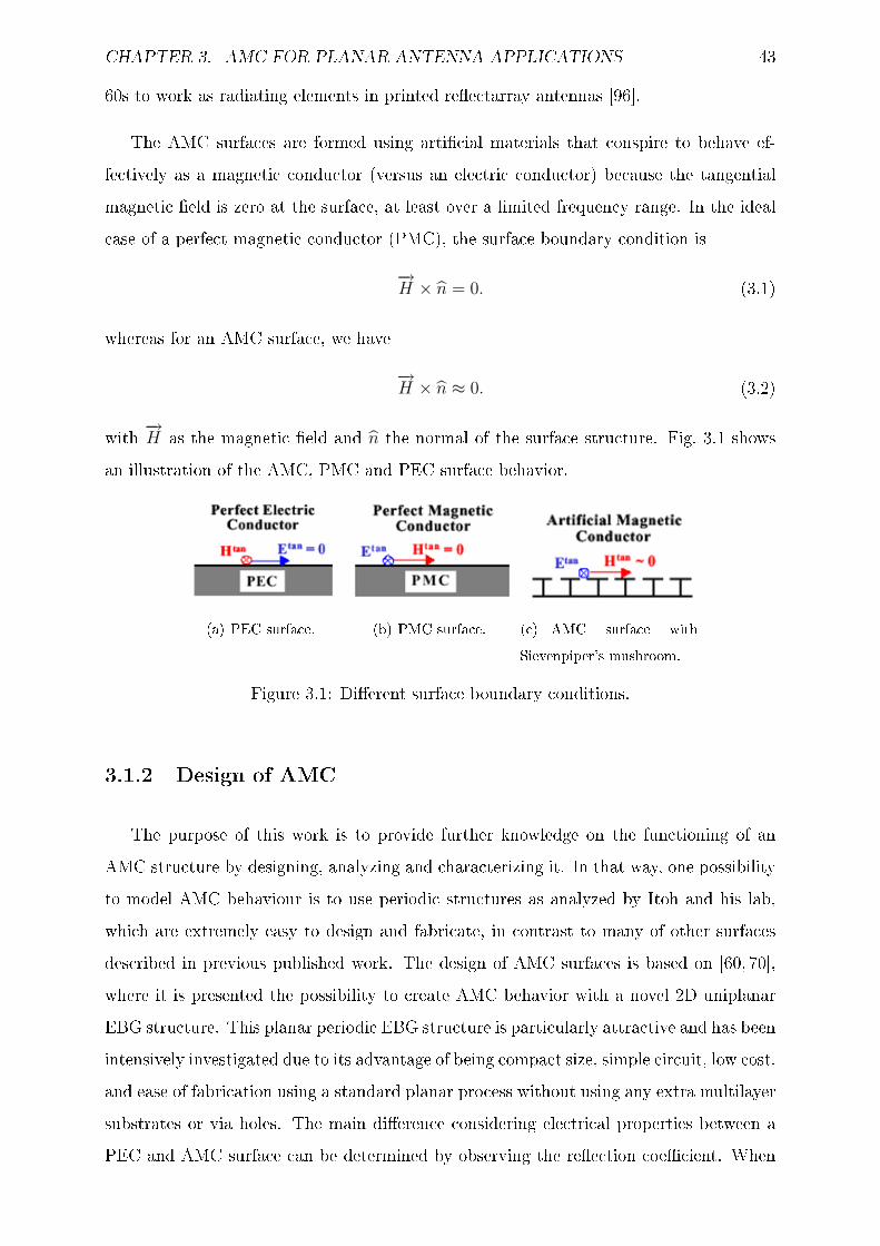
CHAPTER 3. AMC FOR PLANAR ANTENNA APPLICATIONS 43
60s to work as radiating elements in printed reectarray antennas [96].
The AMC surfaces are formed using articial materials that conspire to behave ef-fectively as a magnetic conductor (versus an electric conductor) because the tangentialmagnetic eld is zero at the surface, at least over a limited frequency range. In the idealcase of a perfect magnetic conductor (PMC), the surface boundary condition is
−→H × n = 0. (3.1)
whereas for an AMC surface, we have
−→H × n ≈ 0. (3.2)
with −→H as the magnetic eld and n the normal of the surface structure. Fig. 3.1 showsan illustration of the AMC, PMC and PEC surface behavior.
(a) PEC surface. (b) PMC surface. (c) AMC surface withSievenpiper's mushroom.
Figure 3.1: Dierent surface boundary conditions.
3.1.2 Design of AMC
The purpose of this work is to provide further knowledge on the functioning of anAMC structure by designing, analyzing and characterizing it. In that way, one possibilityto model AMC behaviour is to use periodic structures as analyzed by Itoh and his lab,which are extremely easy to design and fabricate, in contrast to many of other surfacesdescribed in previous published work. The design of AMC surfaces is based on [60, 70],where it is presented the possibility to create AMC behavior with a novel 2D uniplanarEBG structure. This planar periodic EBG structure is particularly attractive and has beenintensively investigated due to its advantage of being compact size, simple circuit, low cost,and ease of fabrication using a standard planar process without using any extra multilayersubstrates or via holes. The main dierence considering electrical properties between aPEC and AMC surface can be determined by observing the reection coecient. When

CHAPTER 3. AMC FOR PLANAR ANTENNA APPLICATIONS 44
applied in the situation of a uniform plane wave normally incident on an AMC plane,this boundary condition produces a reection coecient of +1, with amplitude equal to1 (0 dB) and phase 0, versus -1 for a conventional perfectly electrically conducting PECplane with amplitude 1 (0 dB) and phase 180. Fig. 3.2 illustrated the 2D uniplanar EBGstructure used to realize the AMC surface.
(a) Planar array. (b) Structure unit cell. (c) Circuit model.
Figure 3.2: 2D uniplanar EBG structure used to achieve the AMC surface.
The geometry structure is a square lattice with Jerusalem crosses, which each elementconsists of a metal pad and four connecting branches to form a distributed LC network.These narrow branches together with insets at the connections introduce additional induc-tance, and the gaps between neighboring pads enlarge capacitance. Therefore, the basicidea in that structure is the introduction of a periodic network of parallel LC elements tochange the surface impedance.
The dimensions of the AMC structure working at 12 GHz are summarized in Table 3.1.
Structure dimensionslength a (=lattice constant or period) 7.5 mm
length b 6.5 mmwidth s=g 1 mmwidth h 1.5 mm
Dielectric substratetype Taconic
dielectric constant εr 2.2loss tangent tanδe 0.0009 at f = 10 GHz
dielectric thickness t 1 mm
Table 3.1: EBG structure dimensions for 12 GHz.

CHAPTER 3. AMC FOR PLANAR ANTENNA APPLICATIONS 45
Fig. 3.3 presents the simulated EBG structure unit cell model:
(a) Normal incidence (theta=0). (b) Oblique incidence.
Figure 3.3: 2D uniplanar EBG structure unit cell acting as an AMC surface.
Fig. 3.4 shows the reection coecient (magnitude and phase) when the simulatedAMC surface is impinged upon by a uniform incident plane wave (normal to the surface).A comparison of the results between two commercial electromagnetic softwares (CSTMicrowave Studio and Ansoft High Frequency Structural Simulator (HFSS)) is presented.The CST simulation results agree well in magnitude with the HFSS results. There is adierence in the predicted phase of the reection coecient, that is supposed to be due ofthe dierent methods used in the softwares. CST Microwave Studio use nite integrationtime domain (FITD) method and HFSS use nite element method (FEM). The samedimensions as shown in in Table 3.1 are used in the two models. In Annexe A.1, it isshown the simulation setup of the models in CST and HFSS. The optimum operatingpoint is 12 GHz (the center frequency), where a 0-dB magnitude and a 0 phase in thereection coecient occurs. This corresponds to the operating frequency where the EBGstructure behaves like an AMC surface. The results show that the reection phase ofAMC structures crosses 0 at just one frequency (for one resonant mode). The usefulbandwidth of an AMC is in general dened as +90 to -90 on either side of the centralfrequency, because these phase values would not cause destructive interference betweendirect and reected waves. It is apparent from these results that the EBG structuresbehave as an AMC surface at least within a narrow frequency band near 12 GHz. Theuseful bandwidth between +90 to -90 is of about 5% (11.7 - 12.3 GHz).

CHAPTER 3. AMC FOR PLANAR ANTENNA APPLICATIONS 46
(a) Magnitude. (b) Phase.
Figure 3.4: Reection coecient of the AMC surface under normal incidence (ComparisonCST - HFSS).
Fig. 3.5 illustrates the characterization of the phase of the reection coecient underdierent incident angles with CST.
Figure 3.5: Reection coecient phase of the AMC surface under oblique incidence.
The obtained results show that the performance of the EBG structure as AMC surface,in comparison with dierent AMC surfaces found in the literature, are quite good. InFig. 3.5, the sensitivity of the reection phase with the incident angle is shown. We canobserve that the reection phase of the designed AMC surface change a bit in terms of anoset resonant frequency when the incident angle is larger than 30. Also, the bandwidthis maintained or decreased slightly when the incident angle increases. The performance ofthis AMC structure is sensitive to the frequency, it can only be realized within a narrow

CHAPTER 3. AMC FOR PLANAR ANTENNA APPLICATIONS 47
useful bandwidth. Usually, in the frequency response curve of reection phase, at resonantfrequency we have 0 for AMC; the frequency range is satisfying |phase| < 90 is denedas the available frequency band of AMC in engineering application. These results in termsof reection phase (normal and oblique incidence) agree quite good with what we can ndin the literature in [70] and [97]. As mention previously this surface use a thin substrate incomparison as a dielectric slab (thickness of d = λ0/(4
√εr − 1)), mushroom structure [3],
planar metal square patch [100].
3.2 AMC Surfaces Sidewalls in Parallel-Plate Slot An-tennas
In this work we analyze the eect of a metamaterial denominated ElectromagneticBandGap (EBG) structures acting as if they had articial magnetic conductor (AMC)properties to enhance the main radiation characteristics of parallel-plate slot antennas.The results using these structures in comparison with conventional perfect electric conduc-tor (PEC) sidewalls in a planar slot antenna are presented as an example of application.
3.2.1 Introduction and Motivation
A parallel-plate slot antenna is an attractive candidate for highly-eciency and mass-producible planar phased-array antennas for microwave and millimeter-wave applications.The rst reference to a planar antenna constituted by a parallel plate waveguide structureappears in 1961 [183]. In it, Goebels et al. use a pair of crossed slots as radiating ele-ments, which are excited by one or two modes propagating within the waveguide, basedon if linear or circular polarization is needed. Later, a theory of linear and planar arraysdesign of slots in rectangular waveguides was developed by Elliot [184]. The applica-tions for which were used this type of antennas are mainly radar and communicationsystems. From then, this kind of antennas are described in many general antenna theorybooks [185187]. Nevertheless, it will not be until end of the 70's and beginning of the80's when the great impulse of the parallel plate slot antennas begins. This impulse camefrom Prof. N. Goto and M. Ando from Tokyo Institute of Technology, that opened anwide eld of applications. In these applications already the slots were used on parallel

CHAPTER 3. AMC FOR PLANAR ANTENNA APPLICATIONS 48
plate waveguide structures, excited by a plane front wave, to obtain a linear polarization.Some of these applications can be seen in the Doctoral Thesis of Hirokawa [188] and inlater works of this investigation lab [189]. Recently, diverse works of parallel plate slotantennas have been made in the Radiation Group as the doctoral thesis of Manuel SierraCastañer [15], where several attempts have been made to obtain a uniform quasi-TEMmode within the oversized rectangular waveguides. The feeding structures for parallel-plate slot antennas have been designed and analyzed: stripline network feeding patchesthat excite the planar front wave and slot feed rectangular waveguide connected under theparallel plate waveguide. In both cases, the structure consists of two parallel-plate shortedwith physical metallic walls at the width, existing an important degradation of eld inthe edges of the oversized waveguide due to these walls. Later, the recent investigationof parallel-plate planar antennas constitutes the doctoral thesis of José-Luis Masa [190]that studies new techniques of design and analysis in the planar antennas with parallelplate waveguide structures using microstrip patches as radiating elements.
Generally, the transmission loss in a waveguide is very small in comparison with otherfeedlines such as microstrip line and suspended line. The ideal functioning of the parallel-plate waveguide only propagates a quasi-TEM mode. The excitation of a parallel-plateslot antenna with a quasi-TEM mode for linear polarization has been studied by Ando andHirokawa in [32]. These authors also have rstly analyzed the eld distribution and theaperture illumination in oversized rectangular waveguides for given excitation [191]. Over-sized rectangular waveguides can support a multiplicity of modes. Although a quasi-TEMmode can be generated by a combination of TE modes, it is very dicult to preserve andcontrol the elds in such oversized waveguides in order to achieve a uniform eld patternalong the propagation direction waves. Furthermore, the inherent dispersive behavior ofthe modes makes this quasi-TEM propagation very narrowband. Parallel-plate waveguidehave important disadvantages when they are excited with a TEM or quasi-TEM planewave: the problems is that the eld is not uniform in the entire aperture. The unifor-mity of the electric eld degrades along the propagation direction, becoming slightly weakwith an abrupt decline along the lateral walls because of the PEC sidewalls that closethe structure [192]. This eect produces a degradation of the quasi-TEM mode withinthe oversized waveguides, when they are large (larger than 10 wavelengths) and shortedwith PEC sidewalls. So as mentioned before the key diculty is to predict the innereld in the slotted oversized-rectangular waveguide, which is perturbed by its sidewalls.

CHAPTER 3. AMC FOR PLANAR ANTENNA APPLICATIONS 49
This implies a reduced aperture illumination of the radiating elements and consequentlyreduced aperture eciency in this kind of antennas.
In recent years, there has been increasing interest in using AMC surfaces that showinteresting properties in microwave applications. In 1999, Itoh and his group presentedan important application of AMC surfaces to realize waveguides characterized by a uni-form eld distribution at a specic frequency, referred as quasi-TEM waveguides, or hardwaveguides [68]. The AMC structures nd applications in quasi-optical ampliers [193],high eciency horn antennas [101,194,195] and in sub-wavelength aperture antennas forthe realization of compact planar arrays [103]. In [196], it was shown that a TEM wavepropagation is sustained by arbitrary cross-sectional shape by just using ideal hard bound-ary condition (see subsection 2.4.2) on the walls, thus being well suited for supportinga TEM mode inside waveguides. Also, quasi-TEM conventional rectangular waveguideswith dielectric-loaded sidewalls [197, 198] encounter diculties associated with the needfor high dielectric constants to achieve large uniform-eld apertures, resulting in ad-verse bandwidth reduction. An alternative way was implemented in [199] using printedfrequency selective surface (FSS) on two opposite walls of a conventional rectangularwaveguide. The Antenna Group of Universidad Politécnica de Valencia is also very activein analysis and design of parallel-plate slot antennas. Recently, they have also studiedand analyzed the problematic to control the wave propagation to achieve a uniform dis-tribution along the direction of the wave propagation in oversized waveguides using meta-materials structures with hard/soft surfaces behavior and its application to parallel plateslot antenna to obtain high eciency and directivity in these kinds of antennas [104,105].They have proposed a new guiding structure using a hard surface (see subsection 2.4.2)which forces a quasi-TEM mode to propagate within an oversized rectangular waveguide.This technique lies in suppressing any kind of propagation (higher modes) except theTEM-like one, which can be achieved by using hard surface only at the bottom face ofthe waveguide. The hard surface consists of dielectric-lled longitudinal corrugations orstrips on a grounded dielectric slab arranged periodically on the bottom face surface ofthe waveguide. Also, Ando and his lab at Tokyo Institute of Technology, that openedthe interest in the parallel plate slot antennas, have studied and analyzed new typesof waveguide feeds and performance enhancements of slot-array antennas over oversizedrectangular waveguide with hard-surface sidewalls consisting of a dielectric slab [106].
This work analyzes rst the eect of ideal perfect electric conductor (PEC) and perfect

CHAPTER 3. AMC FOR PLANAR ANTENNA APPLICATIONS 50
magnetic conductor (PMC) within a oversized rectangular waveguide in terms of elddistribution. Then, AMC surfaces that have been placed in the sidewalls of a parallel-plate waveguide in order to provide a more uniform inner-eld distribution in the entireaperture along the lateral walls is presented. The eld distribution and the apertureillumination within the oversized rectangular waveguide for a given excitation is studied.Here, the quasi-TEM mode has been achieved by a combination of TE modes using a slotfeed rectangular waveguide connected under the parallel plate waveguide. A practicalapplication of AMC surfaces in a parallel-plate slot antenna at microwave frequency bandis presented and analyzed in terms of aperture eciency and radiation directivity.
3.2.2 Analysis of the Eect of PEC and PMC Sidewalls in anOversized Rectangular Waveguide
We analyze the eect of PMC sidewalls in a oversized rectangular waveguide as shownin Fig. 3.6
Figure 3.6: Scheme of the rectangular oversized waveguide with two PEC plates and twoPMC walls.
For an oversized rectangular waveguide with PMC walls, we get the following boundaryconditions:
PEC plates =
Ex(y = 0) = Ex(y = b) = 0 ,
Ez(y = 0) = Ez(y = b) = 0 ,(3.3)
PMC walls =
Hy(x = 0) = Hy(x = a) = 0 ,
Hz(x = 0) = Hz(x = a) = 0 ,(3.4)
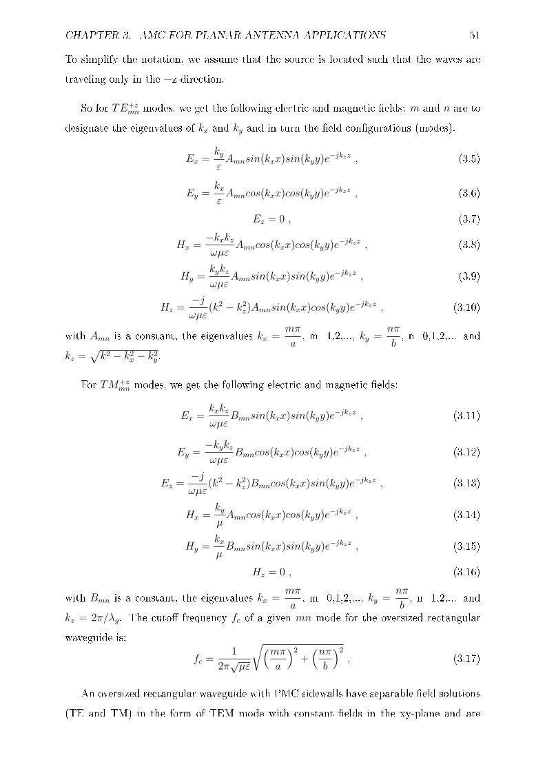
CHAPTER 3. AMC FOR PLANAR ANTENNA APPLICATIONS 51
To simplify the notation, we assume that the source is located such that the waves aretraveling only in the +z direction.
So for TE+zmn modes, we get the following electric and magnetic elds: m and n are to
designate the eigenvalues of kx and ky and in turn the eld congurations (modes).
Ex =ky
εAmnsin(kxx)sin(kyy)e−jkzz , (3.5)
Ey =kx
εAmncos(kxx)cos(kyy)e−jkzz , (3.6)
Ez = 0 , (3.7)
Hx =−kxkz
ωµεAmncos(kxx)cos(kyy)e−jkzz , (3.8)
Hy =kykz
ωµεAmnsin(kxx)sin(kyy)e−jkzz , (3.9)
Hz =−j
ωµε(k2 − k2
z)Amnsin(kxx)cos(kyy)e−jkzz , (3.10)
with Amn is a constant, the eigenvalues kx =mπ
a, m=1,2,..., ky =
nπ
b, n=0,1,2,... and
kz =√
k2 − k2x − k2
y.
For TM+zmn modes, we get the following electric and magnetic elds:
Ex =kxkz
ωµεBmnsin(kxx)sin(kyy)e−jkzz , (3.11)
Ey =−kykz
ωµεBmncos(kxx)cos(kyy)e−jkzz , (3.12)
Ez =−j
ωµε(k2 − k2
z)Bmncos(kxx)sin(kyy)e−jkzz , (3.13)
Hx =ky
µAmncos(kxx)cos(kyy)e−jkzz , (3.14)
Hy =kx
µBmnsin(kxx)sin(kyy)e−jkzz , (3.15)
Hz = 0 , (3.16)
with Bmn is a constant, the eigenvalues kx =mπ
a, m=0,1,2,..., ky =
nπ
b, n=1,2,... and
kz = 2π/λg. The cuto frequency fc of a given mn mode for the oversized rectangularwaveguide is:
fc =1
2π√
µε
√(mπ
a
)2
+(nπ
b
)2
, (3.17)
An oversized rectangular waveguide with PMC sidewalls have separable eld solutions(TE and TM) in the form of TEM mode with constant elds in the xy-plane and are

CHAPTER 3. AMC FOR PLANAR ANTENNA APPLICATIONS 52
independent of the polarization. The TEM solution is a mixture of the lowest order TEand TM modes. The lowest order mode for TE mode is TE10 mode and for TM mode isTM01. Therefore, the dominant mode for both sets of the lowest TE and TM mode is aTEM solution.
As the rst step of the investigation and the design of parallel-plate slot antennas,wave propagation in the oversized rectangular waveguide for given excitation is studied.The oversized rectangular waveguide is part of the feeding structure of the parallel-plateslot antennas. Fig. 3.7(a) and Fig. 3.7(b) show a standard and an oversized rectangularwaveguide working at 12 GHz.
(a) Standard rectangular waveguide (WR75). (b) Oversized rectangular waveguide.
Figure 3.7: Rectangular waveguide working at 12 GHz.
These results are obtained using an ideal excitation (waveguide port) in CST Mi-crowave Studio. Fig. 3.8 depicted the functioning of an oversized waveguide with PECsidewalls excited with an ideal excitation. The main mode is the TE10 mode as in aconventional rectangular waveguide. Note that these results are for an ideal excitationin a oversized waveguide. When we apply PMC boundary condition in the sidewalls ofthe oversized rectangular waveguide, as shown in Fig. 3.9, we observe that a TEM modeis propagated within the waveguide. The electric eld distribution is perfectly uniformin amplitude and phase across and along the structure. These results are very promisingas a novel quasi-TEM guiding structure suitable for feeding planar slot arrays. Thesestructures can support an invariant linear phase-front in a wide waveguide for steerablearray antennas and represent a promising candidate for parallel-plate slot antennas withhigh eciency and directivity.
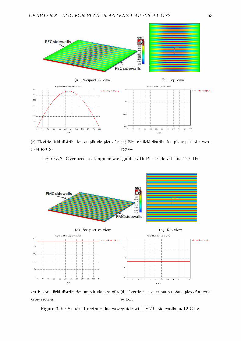
CHAPTER 3. AMC FOR PLANAR ANTENNA APPLICATIONS 53
(a) Perspective view. (b) Top view.
(c) Electric eld distribution amplitude plot of across section.
(d) Electric eld distribution phase plot of a crosssection.
Figure 3.8: Oversized rectangular waveguide with PEC sidewalls at 12 GHz.
(a) Perspective view. (b) Top view.
(c) Electric eld distribution amplitude plot of across section.
(d) Electric eld distribution phase plot of a crosssection.
Figure 3.9: Oversized rectangular waveguide with PMC sidewalls at 12 GHz.

CHAPTER 3. AMC FOR PLANAR ANTENNA APPLICATIONS 54
Usually, the feeding in a oversized rectangular waveguide is generated with N excitingsources that will propagate the quasi-TEM mode within this oversized waveguide. Thisquasi-TEM mode is a combination of TE modes, so it is very dicult to preserve auniform eld pattern (in amplitude and phase) along the propagation axis due to multi-mode propagation. In Fig. 3.10 is shown the electric eld distribution generated by probesources within an oversized waveguide. The probes are set very close from each other. Theripple shown by the transverse eld is associated with the presence of beams. The beamsare due to the exciting probes. It is observed that in Fig. 3.10(b) the PMC sidewalls allowto enhance the uniformity of the eld distribution inside the waveguide.
(a) With PEC sidewalls. (b) With PMC sidewalls.
Figure 3.10: Oversized rectangular waveguide with exciting probes.
3.2.3 AMC Sidewalls in a Parallel-Plate Waveguide
An oversized parallel-plate waveguide consists of two parallel-plate shorted with phys-ical metallic walls at the width. As mentioned in subsection 3.2.1, the disadvantage ofthis kind of structure when you use it as feeding network for planar antennas is the pres-ence of lateral metallic walls that degrade the propagation electromagnetic waves in allthe apertures of the oversized waveguide. This chiey inuences the worst results in theradiation characteristics of the parallel-plate slot antennas. As the rst step of the analy-sis of AMC lateral walls in this kind of antenna, the distribution of electric eld insidethe oversized waveguide with AMC sidewalls is measured. In Fig. 3.11, it is presentedthe experimental setup of the oversized parallel-plate waveguide. The dimensions of thetwo-plate waveguide are 330 x 318 mm with walls all around, where the width of thewaveguide is much longer than the length. The oversized waveguide works in the 12-GHzband. The parallel plate is lled with foam dielectric (εr=1.05) of 7.5 mm thickness, as

CHAPTER 3. AMC FOR PLANAR ANTENNA APPLICATIONS 55
shown in Fig. 3.11. The guided wavelength λg within the parallel-plate waveguide is 24.4mm.
(a) Prole view. (b) Upper view.
(c) Experimental prototype: perspective view (d) Top view
Figure 3.11: Experimental setup used to measure the distribution of the electric eldinside the waveguide.
The end of the oversized waveguide is nished with an absorber material that avoidsreection inside the waveguide. The height between the metal plates should be less than ahalf-wavelength to propagate quasi-TEM modes. A slot-feed waveguide, fed by a coaxialconnector, excites the oversized waveguide. Each one of these slots generates the electricelds (quasi-TEM modes) inside the waveguide. The quasi-TEM modes are travelingwaves propagating from the feed waveguide to the opposite side of the parallel plate.
In Fig. 3.12, it is shown the prototype of the proposed EBG structure placed alongthe lateral walls of the oversized waveguide. In order to measure the eld inside thewaveguide, the upper plate of the waveguide is made of three rows of output connectorsin dierent positions of X, with seven points of measurements in each row across thewaveguide. The distribution of electric eld inside the waveguide could then be measuredusing probes, which are coaxial probes placed approximately 1.5 mm inside it.

CHAPTER 3. AMC FOR PLANAR ANTENNA APPLICATIONS 56
Figure 3.12: EBG structures acting as AMC sidewalls in the parallel-plate waveguide.
The input connector is connected to port 1 of a vector network analyzer (VNA) andthe output connectors (probes) are connected to port 2 of the VNA. By varying the po-sition of the measure probes (output probes) and at the same time measuring S21 withthe VNA at dierent locations across and along the oversized waveguide, the relative elddistribution inside the two-plate waveguide is measured. The comparison between boththe simulated (using CST Microwave Studio) and measured results for the aperture elddistribution throughout the parallel-plate waveguide with conventional metallic walls andwith AMC surface sidewalls at 12 GHz is presented. Fig. 3.13 and Fig. 3.14 show thenormalized S21 parameter, which is proportional to the vertical electric eld (Z-direction),at three sections of the parallel-plate waveguide at the center(X=0), at X = 2λg and X= 3λg distance from the center of the oversized waveguide. When the eld magnitude ismeasured as described below, quite good agreement is observed between the simulationand experimental results in the inner electric eld distribution. The simulated and mea-sured results are obtained with the same setup and boundary conditions. The presenceof the AMC sidewalls in the parallel-plate waveguide results in an enhancement of theeld distribution uniformity along the lateral walls of about 12 dB near the sidewalls(at X=3λg). Therefore, as it moves away from the slot feed waveguide in the oversizedstructure, the enhancement of the electric eld distribution is higher and the eld is moreuniform in all the aperture waveguide. In next subsection it will be shown the quasi-TEMoversized waveguide will excite a planar structure which consists of a planar array of res-onant slots placed at the upper plate waveguide. The use of the lateral AMC walls willproduce the increase of the uniformity eld distribution in the illumination of the radiat-

CHAPTER 3. AMC FOR PLANAR ANTENNA APPLICATIONS 57
ing elements. This improvement increases the aperture eciency of the parallel-plate slotantennas. The ripples observed around the aperture center in both gures are due to thegeneration of the quasi-TEM waves using a slot feed waveguide. These ripples tend to besmooth at the same time as we move away from the slot-feed waveguide.
Figure 3.13: Distribution of electric-eld amplitude measured and simulated at 12 GHzon the top of the parallel-plate waveguide with PEC sidewalls along the X-axis.
Figure 3.14: Distribution of electric-eld amplitude measured and simulated at 12 GHzon the top of the parallel-plate waveguide with AMC sidewalls along the X-axis.

CHAPTER 3. AMC FOR PLANAR ANTENNA APPLICATIONS 58
3.2.4 Antenna Application
In this subsection, the EBG structure acting as AMC surfaces is placed along the lat-eral walls of a parallel-plate slot antenna with linear polarization, as shown in Fig. 3.15 [15].
Figure 3.15: Prototype of the parallel-plate slot antenna used to apply the AMC lateralwalls.
This planar antenna used the distribution waveguide described and analyzed in sub-section 3.2.3 to excite the radiating structure. The radiating elements consist of an arrayof resonant slots that are grabbed on a berglass (εr = 4.8) of thickness 1.6 mm placedin the upper plate of the oversized waveguide. The eective dielectric constant of theantenna is 1.4. The operating frequency of this planar antenna is in the 12-GHz fre-quency band. Some simulations have been realized analyzing the behavior of the AMCsurfaces in the sidewalls of the antenna. The AMC structures were placed inside thedistribution waveguide along the lateral walls. In the simulation and experimental setupthe same boundary conditions for the sidewalls are applied, metallic and AMC surfaceboundary condition. The measured radiation pattern in the E-plane and H-plane at 12GHz are shown in Fig. 3.16 and Fig. 3.17, respectively. It can be observed that a narrowbeamwidth is obtained with the AMC sidewalls in the E- and H-plane.

CHAPTER 3. AMC FOR PLANAR ANTENNA APPLICATIONS 59
Figure 3.16: Measured radiation pattern in the E-plane at 12 GHz.
Figure 3.17: Measured radiation pattern in the H-plane at 12 GHz.
The radiation pattern in the E-plane shows as desired a tilted beam of 6.5 due to theslot design in this plane and the sidelobe levels correspond to an uniform excitation (-13dB). As well, the radiation pattern in the H-plane shows the desired broadside beam. Thisplane is more depending of the uniformity of the eld generated within the parallel-plate

CHAPTER 3. AMC FOR PLANAR ANTENNA APPLICATIONS 60
waveguide. Therefore, the sidelobe levels are smaller with the AMC sidewalls than withthe PEC sidewalls because of a better uniformity in the inner eld distribution. Althoughthe sidelobe levels are in general high due to the feeding network that is not perfectlyuniform and of its phase errors in the excitation respectively, the AMC sidewalls havegiven better results than PEC sidewalls. Also, this can be noticed with the beamwidthcomparing the two results with PEC and with AMC sidewalls. The beamwidth is relatedwith the directivity.
A considerable dierence is observed in Table 3.2 in terms of directivity and apertureeciency among measured and simulated antenna results, this is consequence of the cou-pling of slots and higher modes propagation which in the measurements are higher andso perturbed the inner eld distribution. Also the feeding network of feed slot waveguidewithin the oversized waveguide is not the optimum in terms of generating the quasi-TEMmode and can be also one of the cause of the discrepancies. In spite of the dierentresults between simulation and measurements above mentioned, the obtained results arevery promising. The presence of the AMC sidewalls in the parallel-plate slot antennaprototype results in an enhancement of about 0.3 dB in measurements and of 1.1 dBin simulation in terms of directivity. In the two cases are observed an improvement ofthe directivity because of the aperture illumination of the radiating elements have in-creased. When the planar antenna was measured in the anechoic chamber at UniversidadPolitécnica de Madrid, the experimental results validated the trends predicted from thesimulations, with regard to the improvement of the aperture illumination. It is recom-piled the simulated and the measured results of the parallel-plate slot antennas, as givenin Table 3.2.
f=12 GHz Directivity D [dBi] Aperture eciency ηaperture [%]PEC sidewalls AMC sidewalls PEC sidewalls AMC sidewalls
Simulation 26 27.1 27.5 35.4Measurements 27.3 27.6 37.1 39.8
Table 3.2: Comparison of the directivity and the aperture eciency results for the parallel-plate slot antenna.
The directivity is dened as:
D =4π
λ20
ηaperAaper (3.18)

CHAPTER 3. AMC FOR PLANAR ANTENNA APPLICATIONS 61
Where ηaper is the aperture eciency (≤1) and Aaper is the physical area of the radiat-ing elements, which in this antenna (length L=297 mm and width W=242 mm) is W×L.The maximum estimated directivity for this antenna size at 12 GHz is 31.5 dBi.
3.2.5 Conclusion
The eect of EBG structures acting as if they had AMC properties to enhance waveguidance in oversized waveguides and improve the performance of parallel-plate slot an-tennas has been presented in this work. According to the simulated and measured elddistributions in the parallel-plate waveguide, the results show very satisfactory proper-ties using these structures to enhance and control the wave propagation in this kind ofdistribution waveguide. For that reason, this work has demonstrated the feasibility ofapplying the AMC surface to enhance the properties of the wave propagation in this kindof two-plate waveguides, in order to improve the main radiation characteristics of planarantennas as its directivity. The obtained results let us consider dierent possibilities usingthese congurations to perform planar antennas. Therefore, it represents a promising rststep toward a parallel-plate slot antennas with high eciency and directivity.
Nevertheless, the obtained results could be improved in the future using the solutionthat have been proposed by Universidad Politécnica de Valencia using a hard surfaceplaced at the bottom face of the oversized rectangular waveguide. The hard surfaceallows to suppress any kind of propagation, as higher order modes, except the TEM mode.The combination of AMC sidewalls and a hard surface placed at the bottom face of anoversized rectangular waveguide could be a very good solution to obtain a uniform elddistribution across and along the waveguide and so on increase the aperture illuminationof these kinds of antennas. The proposed two structures represent promising candidatesfor parallel-plate slot antennas with high radiation performances.
3.3 AMC-PEC-AMC Strips in Parallel-Plate Slot An-tennas
In this work, we analyze the eect of articial magnetic conductor (AMC) surfacestrips placed on the bottom face and upper face of an oversized rectangular waveguide

CHAPTER 3. AMC FOR PLANAR ANTENNA APPLICATIONS 62
to enhance the wave guidance within it. An analysis of the eld distribution withinthe waveguide is presented. The results using these congurations in a linear slot arrayantenna fed by a rectangular parallel-plate waveguide in the 12 GHz band are presentedas an example of application. These AMC strips can be a good solution for monomodewaveguides with virtual walls.
3.3.1 Introduction and Motivation
In literature, there exist three kinds of distribution feeding waveguides for parallel-plate slot antennas: the radial waveguide, the oversized parallel-plate waveguide, and therectangular waveguide arrays. This last waveguide consists of two parallel plate delim-ited by physical metallic walls that dene each rectangular waveguides inside the guidedstructure. This kind of feed structure is dierent to the parallel-plate waveguide withpropagation of a TEM plane wave. This feed structure uses an array of monomode TE10
standard rectangular waveguides that distributes the power to the radiating elementswhich are printed in the upper plate as shown in Fig. 3.18. In this case we will have anarray of rectangular waveguides which generate a TE10 mode in each one.
(a) Planar waveguide slot-array anten-nas [200].
(b) Slotted waveguide array at 22 GHz band [201].
Figure 3.18: Rectangular waveguide planar arrays made use of monomode waveguides.
The advantages of the monomode waveguides as a feed structure for parallel-plateslot antennas with respect to TEM front plane wave are that the problem of the uniformeld distribution does not exist as seen in Section 3.2. Nevertheless, when a substrate isadded to implement the radiating elements, this one usually leans on the vertical walls of

CHAPTER 3. AMC FOR PLANAR ANTENNA APPLICATIONS 63
the waveguides. Each rectangular waveguide is not completely isolated from each otherbecause of the diculty of closing perfectly the vertical walls to the radiating elementsubstrate. Therefore, in these vertical apertures, the mutual coupling eld between eachadjacent waveguides is important enough to deteriorate the propagation wave, whichmeans to decrease in the eciency of this kind of antennas. For that reason, a physicalcommunication among them exists that is needed to be solved. Several ways exist tosolve the physical communication between the array of physical rectangular waveguides.One rst possibility is that the problem can be solved generating the vertical walls in themonomode waveguides by means of metalized via holes in a grounded dielectric substrateseparated to a suciently small distances [189, 190]. The problem of this structure isthat it is quite complicated to make because the position and the distance between themetalized via holes are very critic. The breach of these distances causes undesired eectsof reections inside the waveguides. One second possibility is the one that José-Luis Masaproposes in his Doctoral Thesis [190] that consists of the introduction of a new form ofexcitation in the parallel-plate planar antenna, leaving the traditional methodology ofTEM plane wave generation in the oversized waveguide replacing it by a TEN0 modeexcited by a feed waveguide with N exciting sources which in this case are slots as shownin Fig. 3.19(a). The feeding network is formed by a rectangular waveguides array, which iscoupled to the radiating patches by the microstrip coupling horizontal lines placed at thepeak points of the eld inside the waveguide. This feed waveguide is located in the inferiorface of the oversized waveguide and excites the appropriate mode that will propagatewithin this parallel-plate waveguide. The elds can be seen as N TE10 adjacent modeswith opposite phase. Between each TE10 adjacent modes, the electric eld is canceled.A virtual short circuit that delimits the individuals TE10 adjacent modes is observed(Fig. 3.19(a)). In this way, we can understand that the parallel-plate waveguide is madeup of N virtual rectangular waveguides in which a TE10 mode is propagated. We calledthem virtual propagation waveguides because there are no physical walls between eachone. These virtual waveguides have the disadvantage to have mutual coupling. Betweenthese adjacent waveguides, the electric should be canceled but it is not. Therefore, theshort circuit that delimits the TE10 adjacent individual modes is not perfect and it existshigh mutual coupling between each virtual waveguides that degrade the eld generatedwithin the propagation waveguide as shown in Fig. 3.19(b).
CHAPTER 3. AMC FOR PLANAR ANTENNA APPLICATIONS 64
(a) TEN0 modes with virtual short circuits. (b) Simulated results of TEN0 modes (N=19) ina parallel-plate waveguide.
Figure 3.19: Virtual propagation waveguides within a parallel-plate waveguide.
The concept of hard and soft surfaces (see Section 2.4.2), introduced by Kildal [89],allows to control the electromagnetic waves propagation with characteristics of GO andSTOP, respectively, for all the polarizations. The preferred illustration of an ideal soft-hard surface is a PEC/PMC strip grid as a surface with electric and magnetic conductivityin one direction only. The PEC/PMC strip grid represents a hard surface when the stripsare oriented in the same direction as the wave propagates (longitudinal strips), and a softsurface when they are oriented orthogonal to this direction (transverse strips). Recently,several investigations have been dedicated to the planar periodic surfaces used to generatenew boundary conditions and wave guidance properties. These studies have stimulatedseveral applications in the rank of the microwaves and antennas. The works of Kildaland Maci have demonstrated that oriented frequency selective surfaces (FSS) printed ona grounded dielectric slab can obtain these characteristics allowing to guide eciently theelectromagnetic waves propagation [202]. Also, to contribute to the generation equivalentboundary conditions as for example virtual waveguides or AMC surfaces in parallel platewaveguide-wall applications, we propose the use of planar AMC strips in alternates withPEC strips within a parallel-plate waveguide. Its purpose is to enhance, control and guidethe wave propagation of the dierent virtual waveguides in the oversized parallel-platewaveguides and to avoid the undesired eects of mutual coupling among them, being ableto generate virtual short circuits with the AMC/PEC strips delimiting perfectly the TE10
adjacent individual modes in the virtual propagation waveguides. These AMC/PEC stripscould represent a promising rst step toward waveguide slot array with high eciency anddirectivity.
This work analyzes rst the eect of ideal PMC-PEC-PMC strips and real AMC-PEC-

CHAPTER 3. AMC FOR PLANAR ANTENNA APPLICATIONS 65
AMC strip working as propagation strips (virtual propagation waveguide) to control andguide eciently the electromagnetic wave propagation. Then, real prototypes of theseAMC-PEC-AMC strips have been applied and studied as a virtual waveguide and in aoversized waveguide at 12 GHz band. Finally, a practical application of this feed structurein a linear slot array antenna is presented.
3.3.2 Design of the AMC-PEC-AMC Strips
We are going to study and analyze the behavior of AMC-PEC-AMC strips in a parallel-plate waveguide as shown in Fig. 3.20.
Figure 3.20: AMC-PEC-AMC strips cross-section in a parallel-plate waveguide.
These structures are placed inside the parallel plate structure. The fundamental in-terest in using AMC-PEC-AMC strips consists of the possibility to imitate the eect of aconventional standard rectangular waveguide only by using this kind of planar structure,whenever it is in a parallel plate waveguide. The aim of this conguration is the improve-ment of the wave guidance, working as if the whole structure was a virtual waveguide.
The presence of the AMC strips should result in a deep decline of the electric eldto stop the propagation in the transverse direction, as if they were metallic walls of theequivalent real waveguide. However, the PEC strips are going to allow the propagationover it.
To validate that the structure described in Fig. 3.20 works properly, it is necessary to

CHAPTER 3. AMC FOR PLANAR ANTENNA APPLICATIONS 66
simulate a model with a commercial tool software HFSS. The software allows the user toassign specic ideal properties to the faces of dierent surfaces. This facility is used togenerate an ideal PMC-PEC-PMC structure. Then, the real model is simulated. In bothcases, it is going to be considered the values below:
Working frequency: 12.65 GHz.
Total structure dimensions: 305 mm x 65 mm.
Thickness between parallel-plates: 9.5 mm (which correspond to the thickness of astandard rectangular waveguide (WR75) in the 10-15 GHz).
PEC strip width: 19 mm (which correspond to the width of a standard rectangularwaveguide (WR75) in the 10-15 GHz).
Ideal PMC-PEC-PMC Strips
The ideal PMC-PEC-PMC strips model are shown in Fig. 3.21. The PMC surfacesare dened with the Htan=0 condition over it surface.
Figure 3.21: Ideal PMC-PEC-PMC structure.
Fig. 3.22(a) shows the electric eld distribution when the structure is excited with awaveguide port in one edge (x-propagation direction). In the same way, in Fig. 3.22(b),the module of the eld distribution in a cross-section (yz plane) is obtained at 12.65 GHz.

CHAPTER 3. AMC FOR PLANAR ANTENNA APPLICATIONS 67
(a) Electric eld distribution. (b) Electric eld distribution cross-section.
Figure 3.22: Electric eld distribution of the ideal PMC-PEC-PMC strips at 12.65 GHz.
Real AMC-PEC-AMC Strips
Real AMC strips are placed where the ideal PMC strips were in Fig. 3.22. The realAMC strips are achieved by using the printed surfaces with an AMC behavior analyzed inSection 3.1. The real AMC-PEC-AMC strips model are shown in Fig. 3.23. The structureis simulated with HFSS tool.
Figure 3.23: Real AMC-PEC-AMC structure.
The dimensions of the AMC structure working at 12.65 GHz are summarized in Ta-ble 3.3. The characterization by simulation of this AMC structure follows the same designsteps presented in Subsection 3.1.2 and in Annexe A.1.
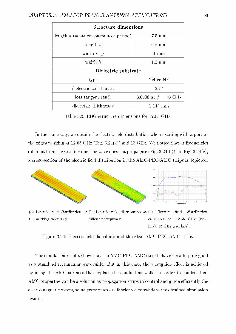
CHAPTER 3. AMC FOR PLANAR ANTENNA APPLICATIONS 68
Structure dimensionslength a (=lattice constant or period) 7.5 mm
length b 6.5 mmwidth s=g 1 mmwidth h 1.5 mm
Dielectric substratetype Neltec NY
dielectric constant εr 2.17loss tangent tanδe 0.0008 at f = 10 GHz
dielectric thickness t 1.143 mm
Table 3.3: EBG structure dimensions for 12.65 GHz.
In the same way, we obtain the electric eld distribution when exciting with a port atthe edges working at 12.65 GHz (Fig. 3.24(a)) and 13 GHz. We notice that at frequenciesdierent from the working one, the wave does not propagate (Fig. 3.24(b)). In Fig. 3.24(c),a cross-section of the electric eld distribution in the AMC-PEC-AMC strips is depicted.
(a) Electric eld distribution atthe working frequency.
(b) Electric eld distribution atdierent frequency.
(c) Electric eld distributioncross-section: 12.65 GHz (blueline), 13 GHz (red line).
Figure 3.24: Electric eld distribution of the ideal AMC-PEC-AMC strips.
The simulation results show that the AMC-PEC-AMC strip behavior work quite goodas a standard rectangular waveguide. But in this case, the waveguide eect is achievedby using the AMC surfaces that replace the conducting walls. In order to conrm thatAMC properties can be a solution as propagation strips to control and guide eciently theelectromagnetic waves, some prototypes are fabricated to validate the obtained simulationresults.

CHAPTER 3. AMC FOR PLANAR ANTENNA APPLICATIONS 69
3.3.3 Single AMC-PEC-AMC Strips in a Parallel-Plate Waveguide
Some simulations have been carried out, analyzing the behavior of the AMC-PEC-AMC strips as components of a virtual rectangular waveguide. The simulations in Sec-tion 3.3.2 showed proper results of this behavior. In the implementation process, twostructures have been built to analyze and validate the simulation results, as it is pre-sented in Fig. 3.25.
(a) AMC-PEC-AMC strips. (b) periodic AMC-PEC-AMC strips.
Figure 3.25: AMC-PEC-AMC structure prototype.
The rst of them (Fig. 3.25(a)) is quite important to validate the theoretical andsimulated results. For this reason, almost all the eorts are going to be placed in this rststructure. Among the dierent ways of measuring the eect of enabling or disabling thepropagation, those which better show the eects and could be performed are presented.In this rst prototype, the AMC-PEC-AMC strips enable the eect of wave guidance,allowing the propagation over the PEC zone, disabling it over the AMC zones.
Coaxial Excitation Analysis
In this assembly, it is supposed to maintain the dimensions used in the previous simu-lation step; in that way, the structure is located between two parallel plates, excited witha coaxial probe, analyzing the eld in a λg ring surrounding the excitation point. Thetest scheme is presented in Fig. 3.26.

CHAPTER 3. AMC FOR PLANAR ANTENNA APPLICATIONS 70
(a) In the cardinal points. (b) Prototype.
Figure 3.26: Experimental setup used to measure the distribution of the electric eld overthe AMC-PEC-AMC strips with a coaxial excitation.
The use of a vectorial network analyzer helps us to verify that the excitation is clearlymatched and to obtain the electric eld amplitude in the dierent points of the ring, ina narrow frequency range (12.4-12.8 GHz). The best results appear at 12.65 GHz. Torepresent the results in a suitable way, two graphs are displayed at 12.65 GHz (Fig. 3.27(a)and Fig. 3.27(b)(b)): for the cardinal points (points 1,2,3 and 4) and for the semicircum-ference (points 2,5,3,6 and 4). As it is seen in Fig. 3.27(a) (cardinal points), points 1 and3 (over PEC) present maximums of transmission, while points 2 and 4 present minimum(over AMC) with a dierence of 20 dB.
(a) In the cardinal points. (b) In the semicircumference.
Figure 3.27: Electric eld distribution amplitude at 12.65 GHz over the AMC-PEC-AMCstrips.

CHAPTER 3. AMC FOR PLANAR ANTENNA APPLICATIONS 71
Uniform Excitation Analysis
In addition to the previous analysis, another test has been done to assure the rightbehavior of the structure. A line is located over the structure without electrical contactwith the AMC-PEC-AMC plane, so that it generates a uniform wave in amplitude prop-agating throughout the plane, as shown in Fig. 3.28(a). Points in a parallel line to thefeed are analyzed for dierent distances from the excitation.
(a) Along the propagation direction. (b) Prototype.
Figure 3.28: Experimental setup used to measure the distribution of the electric eld overthe AMC-PEC-AMC strips with a uniform excitation.
The experimental results showed in Fig. 3.29 verify the eect of wave guidance at 12.65GHz, allowing the propagation over the PEC strip and disabling it over the AMC strips.These results are quite similar to those obtained in simulations, as it was expected.
Figure 3.29: Electric eld distribution amplitude at 12.65 GHz along the propagationdirection over the AMC-PEC-AMC strips.

CHAPTER 3. AMC FOR PLANAR ANTENNA APPLICATIONS 72
The results are quite satisfactory comparing the behavior of virtual waveguides prop-agating TE10 mode with the one in a standard rectangular waveguide with the samedimensions. The presence of the AMC structures in the measurements causes a deepdecline of the eld of about 20 dB along this surface.
The width of the AMC surface is an important parameter for the proper functioning ofthe structure. The results presented in this work are done over a structure of four periodsof AMC (see Fig. 3.25). However, it is simulated some other structures with less thanfour periods of AMC (two and three). In these cases, the results were not good enough,noticing that the eld declines over the AMC surfaces is directly related to the numberof periods of the AMC structure. Also, propagation of surface waves can be one of thereason of the necessity to put four periods to get a quite good results. Putting vias in theAMC structures will allow to cancel the surface waves propagation and so have a betterbehaviour of the structure. In a future work, a prototype of AMC structures with viaswill be realized and measured to compare the behavior.
3.3.4 Periodic AMC-PEC-AMC Strips in an Oversized Rectan-gular Waveguide
At last, measurements of the prototype 2 are presented. Periodic AMC-PEC-AMCstrips are applied in an oversized structure described before to avoid the presence ofmetallic walls for each rectangular waveguide as shown in Fig. 3.30. Because of theexcitation (which is a slot feed waveguide) and its narrow bandwidth, measurementsare only related to 12.65 GHz (one of the working frequencies). Measured results show aproper behavior (see Fig. 3.31). Because of the convincing simulated and measured resultsobtained with a single AMC-PEC-AMC strip in parallel plate waveguide, it is appliedseveral structures working such as consecutive virtual waveguides. It is observed the samebehavior as before with a same decline of the eld of about 20 dB. These experimentalresults validate the simulations and measurements obtained in the rst prototype of asingle AMC-PEC-AMC strip. The periodic AMC-PEC-AMC strips could be applied inparallel plate slot antennas to guide and control the propagation waves.

CHAPTER 3. AMC FOR PLANAR ANTENNA APPLICATIONS 73
(a) Prole view. (b) Top view.
(c) Experimental prototype. (d) Measurement setup.
Figure 3.30: Experimental setup used to measure the electric eld distribution over theperiodic AMC-PEC-AMC strips within the oversized waveguide.
Figure 3.31: Measured electric eld distribution at the frequency working (12.65 GHz)across and along the propagation direction (x-direction) over the periodic AMC-PEC-AMC structure inside the oversized waveguide.

CHAPTER 3. AMC FOR PLANAR ANTENNA APPLICATIONS 74
3.3.5 Antenna Application
To validate all the previous results, it is decided to design a quite simple planarantenna, in which our AMC-PEC-AMC waveguide (prototype 1) is going to work asthe feeding stage. One of the easiest models that can be thought about is a linear slotarray excited by the AMC-PEC-AMC strips as a feed waveguide as it may be seen inFig. 3.32(b). The feed waveguide is excited at one side by a coaxial probe. The value of theguided wavelength (λg) inside the waveguide, considering all the materials in Fig. 3.32(a),is fundamental when designing the linear slot array. The radiating elements consist ofseventeen linear resonant slot arrays. The length of the slots are L=0.485λg. The slotshave an oset from the center of 3.1 mm (in ± y-direction) and between each other of λg/2(in x-direction). The width of the slots are W=L/10. The value of the guided waveguideis λg = 24.3 mm for the layer distribution inside the structure at 12.65 GHz. Afterward,the slot layer is simulated, prototyped, and assembled with the rest of the components ofthe slot antenna. Fig. 3.32(b) shows the manufactured antenna, after the assembly of thedierent parts. The antenna device is measured in the anechoic chamber of the researchgroup. The return loss measurement of the linear slot array antenna with AMC-PEC-AMC strips in comparison with simulation of standard rectangular waveguide (WR75)as guiding structure are presented in Fig. 3.33. We do not compare the measurementswith the simulation of the linear slot array antenna with AMC-PEC-AMC strips becauseof the long computational time. The reection at 12.65 GHz is less than -20 dB inmeasurements with AMC-PEC-AMC strips and less than -35 dB in simulation with thestandard waveguide. This comparison is only to show the viability of AMC-PEC-AMCstrips as guiding feed structure like the conventional rectangular waveguide in this kindof antennas.

CHAPTER 3. AMC FOR PLANAR ANTENNA APPLICATIONS 75
(a) Assembly scheme. (b) Antenna prototype.
(c) Measurement setup at anechoicchamber from Technical University ofMadrid.
Figure 3.32: Linear slot array antenna with AMC-PEC-AMC strips as a feed structure.
12 12.2 12.4 12.6 12.8 13−40
−35
−30
−25
−20
−15
−10
−5
0
Frequency [GHz]
Ret
urn
loss
[dB
]
Measurements: AMC−PEC−AMC stripsSimulation CST: standard rectangular waveguide (WR75)
Figure 3.33: Return loss of the linear slot array antenna: comparison of AMC-PEC-AMCstrips and standard rectangular waveguide (WR75) as a guiding structure.

CHAPTER 3. AMC FOR PLANAR ANTENNA APPLICATIONS 76
Finally, the radiation pattern is measured in the anechoic chamber at 12.65 GHzfor AMC-PEC-AMC strips and compared with the radiation pattern of the simulatedlinear slot array antenna with a standard rectangular waveguide as a feed structure (seeFig. 3.34).
−90−80−70−60−50−40−30−20−10 0 10 20 30 40 50 60 70 80 90−50
−45
−40
−35
−30
−25
−20
−15
−10
−5
0
Theta [deg.]
Am
plitu
de [d
B]
Measurements: AMC−PEC−AMC stripsSimulation CST: standard rectangular waveguide (WR75)
(a) Horizontal radiation pattern in the E-plane (ar-ray): CP (solid line) and XP (dashed line).
−90−80−70−60−50−40−30−20−10 0 10 20 30 40 50 60 70 80 90−50
−45
−40
−35
−30
−25
−20
−15
−10
−5
0
Theta [deg.]
Am
plitu
de [d
B]
Measurements: AMC−PEC−AMC stripsSimulation CST: standard rectangular waveguide (WR75)
(b) Vertical radiation pattern in the H-plane (slot):CP (solid line) and XP (dashed line).
Figure 3.34: Radiation pattern of the linear slot array antenna at 12.65 GHz: comparisonof AMC-PEC-AMC strips and standard rectangular waveguide (WR75) as a guiding feedstructure.
The horizontal radiation pattern (Fig. 3.34(a)) (xz plane) has some phase errors andhigher sidelobe levels due to the AMC-PEC-AMC strip guiding structure. The verticalradiation pattern (Fig. 3.34(b)) (yz plane) shows ripples in the measurements due to thefeeding waveguide (the AMC-like walls decrease the electric eld but they do not stopall the propagation and this eect cannot be neglected) and because of the nite groundplane in the xy plane which cause edge diraction. Although the radiation pattern hasto be improved, measurements demonstrate the proper operation of an antenna with anAMC-PEC-AMC waveguide as the feeding stage.
3.3.6 Conclusion
The eect of AMC-PEC-AMC strips to enhance wave guidance in parallel platewaveguides has been presented in a practical application. For this reason, this workincludes some software simulations and the prototype measurements and evaluations.The measurements show promising results in using these structures to enhance, control,

CHAPTER 3. AMC FOR PLANAR ANTENNA APPLICATIONS 77
and guide the wave propagation in oversized parallel plate waveguides, achieving virtualpropagation TE10 mode waveguide (with no physical walls) being able to generate vir-tual short circuit. The propagation strips as guidance feeding network of a linear slotarray antenna show also quite good results in terms of radiation characteristics. Also,the periodic AMC-PEC-AMC strips as an array of monomode waveguides have been an-alyzed and showed good results, working like consecutive virtual waveguides, delimitingthe TE10 adjacent individual modes propagation avoiding high undesired mutual couplingbetween each virtual rectangular waveguide. The main inconvenient that has been shownis the need of four periods of AMC to get convenient results. If less than four periodsof AMC are used, the results were not good enough as virtual waveguides. Putting viasin the AMC structures will allow to cancel the surface waves propagation and so have abetter behavior of the structure. In a future work, these AMC structures with vias willbe realized and measured to compare the behavior. These AMC-PEC-AMC strips arevery attractive and can reduced considerably the manufacturing complexity of an arrayof monomode waveguides for steerable array antennas.
This work demonstrates the feasibility of applying the AMC-PEC-AMC strip cong-uration in parallel plate waveguides to enhance the properties of the wave propagation.In the case of using several AMC-PEC-AMC structures working like consecutive virtualwaveguides in a plane, it is reduced the coupling between each other. The results obtainedlet us consider dierent possibilities using this architecture to perform planar antennaswith specic features.
For a future practical application, our aim will be to apply these structures to enhancethe main radiation characteristics of the parallel plate planar antennas as aperture e-ciency and radiation directivity. As the rst step of the investigation and the design ofthis kind of planar antennas, wave propagation in the oversized parallel plate waveguidefor given excitation is studied.


Chapter 4
Planar Left-Handed (LH) Lens forPlane TEM Wave Excitation inParallel-Plate Slot Antennas
In parallel-plate slot array antennas, the most important part of the antenna is thefeeding network. The excitation system (oversized waveguide) is the one which distributesthe desired amplitude and phase from the feed structure to the radiating elements depend-ing on the radiation pattern to synthesize. The feeding structure generates the electricelds inside the oversized waveguide to obtain the radiation pattern. The ideal function-ing of the oversized parallel-plate waveguide propagates a quasi-TEM mode. This typeof eld distribution propagation is useful for having a uniform feeding of the oversized-rectangular waveguide slot array antenna with high-eciency. The traditional TEM wavehas advantage in terms of slot arrangement as radiating elements for linearly polarizedradiation. During the last years, it has been developed dierent excitation structures toachieve a uniform feeding for this kind of antennas.
This chapter presents and analyzes a way to feed parallel-plate slot antennas withTEM wave excitation in order to enhance the uniform eld distribution inside the parallelplate waveguide structure, as well as to improve the aperture eld illumination of theradiating elements. This form of excitation for parallel-plate slot antennas based on aplanar left-handed metamaterial lens excited via a coaxial probe is designed, analyzed andcharacterized as a feeding to generate a quasi-TEM mode within the oversized rectangular
79

CHAPTER 4. PLANAR LH LENS IN PARALLEL-PLATE SLOT ANTENNAS 80
waveguide. Two prototypes are designed: one in the 7.5 GHz band and the second workingin the 12 GHz frequency band. This feed structure is very attractive for parallel-plate slotantennas due to its advantage of being simple and can be fabricated using planar processtechnology.
4.1 Introduction and Motivation
Slot array antennas set up on rectangular parallel-plate waveguides are widely usedas their designs leads to high gain and high eciency. Furthermore, their fabricationprocess is easy and repeatable. The fundamental part that all this kind of antennas havein common is the oversized rectangular parallel-plate waveguide, which uses the waveguidesystem to feed the radiating elements (etched slot on a upper conductor plate in this case).The feeding network of these antennas is constituted by the oversized waveguide and thefeed that generate the eld propagation within it. As described in the literature, thereare many ways to excite a plane wave in a oversized parallel-plate waveguide [32, 189].Moreover, the excitation by conventional rectangular waveguide fed slots (see Fig. 4.1(a))or by excitation network constructed in microstrip technology (see Fig. 4.1(b)) do notgenerate a pure uniform TEM plane wave because of the discretization of the feedingelements. So, the uniformity of the eld distribution is not preserved along the directionof the propagation mode in the oversized waveguide. In this last two cases stated inFig. 4.1, the basic principle to generate a TEM mode is the same. N elements, used toinduce the eld, acts as sampling elements of this. The more excitation points are utilized,the more uniform the TEM mode emerges and the less ripples of the inner eld in theoversized waveguide occur. Therefore, the excitation of the dominant quasi-TEM modein such structures is problematic.
Recently, there has been increasing interest in using metamaterial structures thatpresent properties not commonly found in nature. In particular, left-handed (LH) meta-materials exhibit a negative permittivity and permeability simultaneously, leading to anegative refractive index (see Subsection 2.4.3). The negative refractive index of a left-handed medium can appear as negative while the index refraction of the constituentsstill remains positive. As a consequence, these arrangements have attracted considerablyattention in the last eight years since promising new applications in the eld of antennas

CHAPTER 4. PLANAR LH LENS IN PARALLEL-PLATE SLOT ANTENNAS 81
and microwaves, for example, in the design of novel types of perfect lenses [125] and inthe generation of supercial plasmas in the microwave range for applications in planarantennas [145]. Lenses consisting of LH medium are not a new concept; back in 1968,Veselago discussed the possibility of LH medium-based lenses in his renowned paper [118]which theorized the existence of LH materials. In addition, LH medium-based microwavelenses have been mentioned in various books [185,203].
(a) Excitation by a feed slot conven-tional rectangular waveguide [15].
(b) Excitation by a linear arrays of microstrippatches [18].
Figure 4.1: Dierent excitation methods of TEM mode for parallel-plate waveguide slotarrays.
As an example, a lens made from LH materials that would be converging if madefrom conventional material, will be diverging, and vice versa. One of the most popularapplications of metamaterials belongs to the fabrication of planar lenses. Also the worksof Caloz et al. propose a periodic planar structure that consists of a square patch withvia holes in form of "mushroom" (Sievenpiper's mushroom) that allows a left-handed be-havior, whose characteristics are that their permittivity and its permeability are negativewhereas the electrical properties of the constituent parts (substrate) are positive [142].The proposed developments are the design of new types of planar lenses [143,144]. Also,Engheta and Ziolkowski have done some numerical studies of plano-concave LH lensesto present their advantages in comparison with traditional lenses [134]. In general, theshape of optical lenses is the one which denes their attributes, and for several specialappliances this shape is complicated to fabricate. The advantage of these metamaterialsis that they enable the construction of planar lenses which permit to focus light on tiny
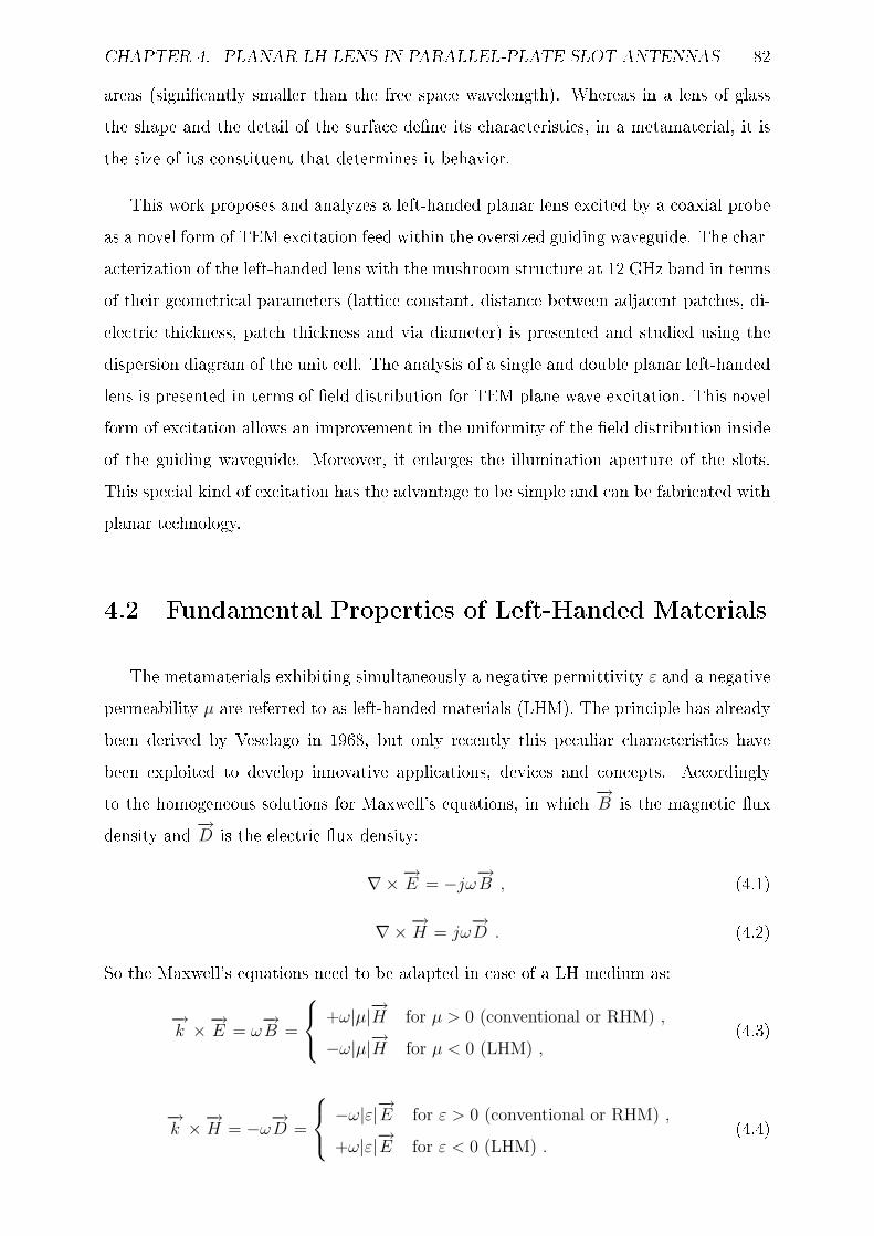
CHAPTER 4. PLANAR LH LENS IN PARALLEL-PLATE SLOT ANTENNAS 82
areas (signicantly smaller than the free space wavelength). Whereas in a lens of glassthe shape and the detail of the surface dene its characteristics, in a metamaterial, it isthe size of its constituent that determines it behavior.
This work proposes and analyzes a left-handed planar lens excited by a coaxial probeas a novel form of TEM excitation feed within the oversized guiding waveguide. The char-acterization of the left-handed lens with the mushroom structure at 12 GHz band in termsof their geometrical parameters (lattice constant, distance between adjacent patches, di-electric thickness, patch thickness and via diameter) is presented and studied using thedispersion diagram of the unit cell. The analysis of a single and double planar left-handedlens is presented in terms of eld distribution for TEM plane wave excitation. This novelform of excitation allows an improvement in the uniformity of the eld distribution insideof the guiding waveguide. Moreover, it enlarges the illumination aperture of the slots.This special kind of excitation has the advantage to be simple and can be fabricated withplanar technology.
4.2 Fundamental Properties of Left-Handed Materials
The metamaterials exhibiting simultaneously a negative permittivity ε and a negativepermeability µ are referred to as left-handed materials (LHM). The principle has alreadybeen derived by Veselago in 1968, but only recently this peculiar characteristics havebeen exploited to develop innovative applications, devices and concepts. Accordinglyto the homogeneous solutions for Maxwell's equations, in which −→B is the magnetic uxdensity and −→D is the electric ux density:
∇×−→E = −jω−→B , (4.1)
∇×−→H = jω−→D . (4.2)
So the Maxwell's equations need to be adapted in case of a LH medium as:
−→k ×−→E = ω
−→B =
+ω|µ|−→H for µ > 0 (conventional or RHM) ,
−ω|µ|−→H for µ < 0 (LHM) ,(4.3)
−→k ×−→H = −ω
−→D =
−ω|ε|−→E for ε > 0 (conventional or RHM) ,
+ω|ε|−→E for ε < 0 (LHM) .(4.4)
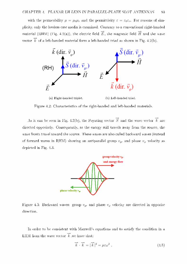
CHAPTER 4. PLANAR LH LENS IN PARALLEL-PLATE SLOT ANTENNAS 83
with the permeability µ = µ0µr and the permittivity ε = ε0εr. For reasons of sim-plicity, only the lossless case media is examined. Contrary to a conventional right-handedmaterial (RHM) (Fig. 4.2(a)), the electric eld −→E , the magnetic eld −→H and the wavevector −→k of a left-handed material form a left-handed triad as shown in Fig. 4.2(b).
(a) Right-handed triplet. (b) Left-handed triad.
Figure 4.2: Characteristics of the right-handed and left-handed materials.
As it can be seen in Fig. 4.2(b), the Poynting vector −→S and the wave vector −→k aredirected oppositely. Consequently, as the energy still travels away from the source, thewave fronts travel toward the source. These waves are also called backward waves (insteadof forward waves in RHM) showing an antiparallel group vgr and phase vϕ velocity asdepicted in Fig. 4.3.
Figure 4.3: Backward waves: group vgr and phase vϕ velocity are directed in oppositedirection.
In order to be consistent with Maxwell's equations and to satisfy the condition in aLHM from the wave vector −→k ,we have that:
−→k · −→k = |−→k |2 = µεω2 , (4.5)

CHAPTER 4. PLANAR LH LENS IN PARALLEL-PLATE SLOT ANTENNAS 84
and hencek2
ω2= µε , (4.6)
k
ω= ±√µε . (4.7)
It makes sense to choose the negative square root if µ and ε are a negative value at thesame time. From (4.7), we have:
k
ω= −√µε , (4.8)
and knowing that the refractive index n is dened as
n =kc
ω, (4.9)
with c = 1√µ0µrε0εr
is the speed of light in the medium. Finally, we get the negativerefractive index in a left-handed material:
nLH =√
(−µr)(−εr) = −√µrεr . (4.10)
In consequence to the left-handed sense, all phenomena associated with electromagneticwave propagation in material have to be reconsidered as mentioned in Subsection 2.4.3.Fig. 4.4 illustrated the behavior of the medium depending of the values of the permittivityε and permeability µ. Materials that reside in quadrants I, II and IV are known to existin nature.
Figure 4.4: Properties of mediums depending of ε and µ [6].

CHAPTER 4. PLANAR LH LENS IN PARALLEL-PLATE SLOT ANTENNAS 85
4.3 Design of the Feeding Structure
4.3.1 Analysis and Design of the Planar LH Lens
The feeding structure is a planar left-handed lens excited by a coaxial probe and inter-sected by a conventional dielectric with a parabolic LH/RH interface as shown in Fig. 4.5.The interaction between a LH medium and a conventional one (right-handed (RH)) withequivalent electromagnetic densities (refractive index: nRH = −nLH) and with parabolicinterface has recently been successfully demonstrated to perform a transformation fromcylindrical to plane waves and vice versa. Since LH medium-based lenses have a negativerefractive index, the parabolic LH/RH interfaces (boundary between media of refractiveindices with opposite signs) required to converge or diverge electromagnetic waves and soon are dierent than conventional (i.e. RH) lenses. In fact, a convex LH medium-basedlens diverges radiation while a concave LH medium-based lens converges radiation in aRH environment [144].
(a) Concept of transformation from cylindricalwave to plane wave.
(b) Comparison between a conventional par-abolic reector (O-P-R) and a parabolicRH/LH refractive interface (O-P-R').
Figure 4.5: Principle of focusing by a parabolic LH/RH refractive interface.
The parabola is a ubiquitous shape and well-known for its focusing capabilities in elec-tromagnetic applications, as for example the traditional parabolic reectors with feeder

CHAPTER 4. PLANAR LH LENS IN PARALLEL-PLATE SLOT ANTENNAS 86
for satellite communications: parallel rays incident upon a parabolic reector convergeat the focal point [185]. In this kind of antennas the transmitted and the received wavesalways propagate on the concave side of the parabola and the reector transform a cylin-drical wave into a plane wave. Nevertheless, from the reciprocity principle, in this casethe parabolic LH/RH interface, which is not a metallic surface, allows the refracted raysinstead of reected rays, so that the cylindrical wave into a plane one from one side to theother side of the interface is observed and depicted in Fig. 4.5(a). This concept is quiteunderstandable looking at Fig. 4.5(b), where the reection path O-P-R, achieved with aconventional parabolic reector, is replaced by the refraction path O-P-R' leading to theeect depicted in Fig. 4.5(a). If the interface is not perfectly matched (nRH 6= −nLH),part of the energy is reected and the plane wave transformation is not so perfect. Asshown in Fig. 4.5(b), it is possible to excite via a coaxial probe a cylindrical wave in thefocal point O that will be transform in a plane wave at the other side of the parabolicLH/RH interface.
The parabolic shape is designed by the ray analysis of geometrical optics in particularby Fermat's principle, which has to be reconsidered due to negative refractive index ofthe LH medium. Thus, the condition to achieve the cylindrical wave into plane wavetransformation, according to Fermat's principle, can be obtained by applying the opticalpath length technique as shown in Fig. 4.5(b) and (4.11):
OP + PP ′ = OQ , (4.11)
Then, we have:rnLH + nRH(f − r cos θ) = nLHf , (4.12)
where nLH is the refractive index of the left-handed medium and nRH is the refractiveindex of the right-handed medium. Therefore, the radius r of the parabolic interface is:
r =f(nLH − nRH)
nLH − nRH cos θ, (4.13)
and the focal distance f of the parabola in terms of r is:
f =r(nLH − nRH cos θ)
nLH − nRH
. (4.14)
As seen in (4.14), the conventional parabola function for focusing at a distance f [185] ismodied due to the LH medium with negative refractive index. The parabolic RH/LH in-terface allows to reduce the parabola dimensions in comparison with conventional parabola.

CHAPTER 4. PLANAR LH LENS IN PARALLEL-PLATE SLOT ANTENNAS 87
There are two distinct advantages of using LH lenses over conventional lenses in a RHenvironment. First, a LH lenses has a larger radius of curvature r compared to a con-ventional lens with the same magnitude of refractive index n and focal distance f (see(4.14)), which translates to reduced aberration. The next advantages are that LH lensescan be matched to the surrounding RH medium when nRH = −nLH and µr,RH/εr,RH =µr,LH/εr,LH . As a result, parabolic lenses can be reectionless; all incident electromagneticwaves are allowed to pass through the LH/RH interface. In order to obtain focusing, themagnitude of the refractive index of both mediums should be:
nRH = −nLH , (4.15)
which implies from (4.10) that
εr,RHµr,RH = εr,LHµr,LH , (4.16)
In addition a perfect matching between the two mediums (RH and LH) should happen toavoid reection, which requires that the characteristic impedances of the two media are:
ZRH = ZLH , (4.17)
which implies thatµr,RH
εr,RH
=µr,LH
εr,LH
, (4.18)
Therefore, the permittivity εr and permeability µr of the LH material should be designedaccurately for a good matching between the RH and LH medium and avoid undesiredreections..
4.3.2 Ideal LH Lens
Ideal Single Lens
The ideal model of the planar LH lens is illustrated in Fig. 4.6. The model of idealLH lens is rst created to study the conversion of the cylindrical waves into plane wavedescribed in Subsection 4.3.1. The model is composed of the parabolic interface placedbetween the LH medium (ideal eective homogeneous medium with the constitutive pa-rameters εr,LH = −1 and µr,LH = −1 and the RH medium (dielectric foam of a 8 mmthickness with the constitutive parameters εr,RH = 1 and µr,RH = 1, which is inserted in

CHAPTER 4. PLANAR LH LENS IN PARALLEL-PLATE SLOT ANTENNAS 88
the oversized rectangular waveguide. The feed waveguide is a parallel-plate waveguide oflength 380 mm and width 305 mm with metallic side walls. The excitation is realized bya coaxial probe situated in the focal point (focal distance f of the parabola = 76 mm)of the planar LH lens. The operating frequency of the lens is in the frequency band of12 GHz. The full-wave simulations are carried out by the nite element method (FEM)simulation software HFSS v.10 that allows to dene negative ideal eective homogeneousparameters for the LH material.
Figure 4.6: Planar LH single lens with ideal constitutive parameters.
In Fig. 4.7(a) and Fig. 4.7(b), the simulated results of the ideal single lens are ex-posed in amplitude and in phase. An excellent conversion from spherical to plane waveis observed due to the condition of the equal electromagnetic densities of the two mediaapplying an ideal eective homogeneous LH medium (εr,LH = µr,LH = −1). This condi-tion allows to adjust the interface between the two media in the way to avoid undesiredreections in order to obtain a perfect transformation to a plane uniform wave front inamplitude and phase.
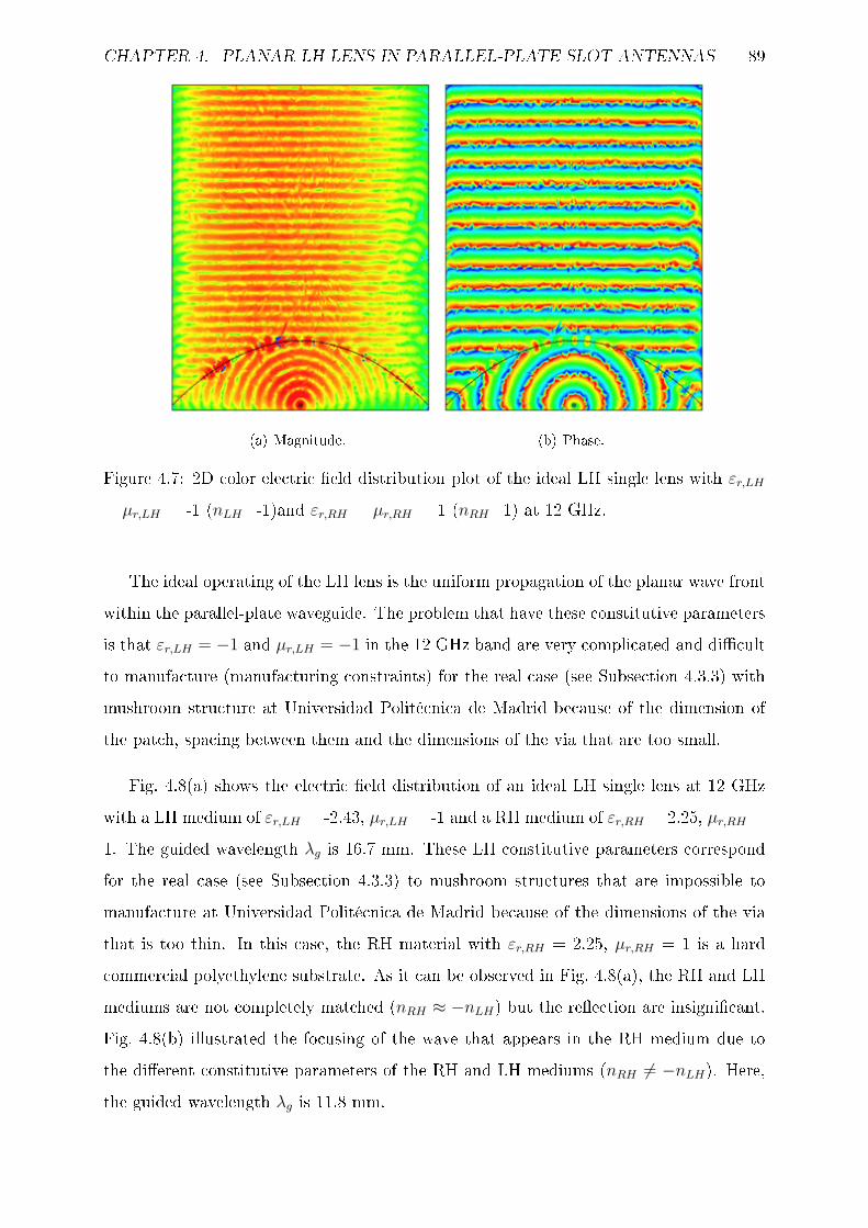
CHAPTER 4. PLANAR LH LENS IN PARALLEL-PLATE SLOT ANTENNAS 89
(a) Magnitude. (b) Phase.
Figure 4.7: 2D color electric eld distribution plot of the ideal LH single lens with εr,LH
= µr,LH = -1 (nLH=-1)and εr,RH = µr,RH = 1 (nRH=1) at 12 GHz.
The ideal operating of the LH lens is the uniform propagation of the planar wave frontwithin the parallel-plate waveguide. The problem that have these constitutive parametersis that εr,LH = −1 and µr,LH = −1 in the 12 GHz band are very complicated and dicultto manufacture (manufacturing constraints) for the real case (see Subsection 4.3.3) withmushroom structure at Universidad Politécnica de Madrid because of the dimension ofthe patch, spacing between them and the dimensions of the via that are too small.
Fig. 4.8(a) shows the electric eld distribution of an ideal LH single lens at 12 GHzwith a LH medium of εr,LH = -2.43, µr,LH = -1 and a RH medium of εr,RH = 2.25, µr,RH =1. The guided wavelength λg is 16.7 mm. These LH constitutive parameters correspondfor the real case (see Subsection 4.3.3) to mushroom structures that are impossible tomanufacture at Universidad Politécnica de Madrid because of the dimensions of the viathat is too thin. In this case, the RH material with εr,RH = 2.25, µr,RH = 1 is a hardcommercial polyethylene substrate. As it can be observed in Fig. 4.8(a), the RH and LHmediums are not completely matched (nRH ≈ −nLH) but the reection are insignicant.Fig. 4.8(b) illustrated the focusing of the wave that appears in the RH medium due tothe dierent constitutive parameters of the RH and LH mediums (nRH 6= −nLH). Here,the guided wavelength λg is 11.8 mm.

CHAPTER 4. PLANAR LH LENS IN PARALLEL-PLATE SLOT ANTENNAS 90
(a) Magnitude: with εr,LH = -2.43, µr,LH
= -1 (nLH=-1.56) and εr,RH = 2.25, µr,RH
= 1 (nRH=1.5).
(b) Magnitude: with εr,LH = -10.24, µr,LH
= -1 (nLH=-3.2) and εr,RH = 4.5, µr,RH =1 (nRH=2.1).
Figure 4.8: 2D color electric eld distribution plot of the ideal LH single lens with dierentconstitutive parameters at 12 GHz.
A second prototype for the real LH lens with mushroom structures (see Subsec-tion 4.3.3) in the 7.5 GHz band is analyzed. Some simulation results in terms of 2Dcolor plot and E-eld distribution within the parallel-plate waveguide for the ideal LHlens at 7.5 GHz are presented in Fig. 4.9 and Fig. 4.10. The guided wavelength λg is 26.7mm. In Fig. 4.9, the RH and LH medium are completely matched (nRH = −nLH), but itis dicult to have exactly εr,LH = -2.25, µr,LH = -1 in the real LH lens with the mush-room structures, but we manage to get εr,LH = -2.43, µr,LH = -1 (see Subsection 4.3.3) aspresented in Fig. 4.10. In Fig. 4.10(b), we can observe the electric eld distribution alongthe propagation direction X at a distance of 4λg, 8λg and 12λg from the coaxial probe.These results testify a regular uniform conversion from cylindrical to plane wave in thecenter of the parallel plate waveguide, whereas along the propagation direction the planewave front is not that uniform. This can be from the fact that the equal electromagneticdensities (nRH = −nLH) of the both media is not adapted perfectly. Hence, the interface(parabola shape) and the two media are not absolutely conform (that is discretized inHFSS software and is not perfectly parabolic) they provoke undesired reections, andfor which the transformation in a plane wave is not accomplished in a totally uniformmanner.

CHAPTER 4. PLANAR LH LENS IN PARALLEL-PLATE SLOT ANTENNAS 91
(a) 2D color plot in magnitude. (b) Distribution of electric-eld amplitude within theparallel-plate waveguide along the propagation direction X.
Figure 4.9: Electric eld distribution plot of the ideal LH single lens with εr,LH = -2.25,µr,LH = -1 (nLH=-1.5) and εr,RH = 2.25, µr,RH = 1 (nLH=1.5) at 7.5 GHz.
(a) 2D color plot in magnitude. (b) Distribution of electric-eld magnitude within theparallel-plate waveguide along the propagation direction X.
Figure 4.10: Electric eld distribution plot of the ideal LH single lens with εr,LH = -2.43,µr,LH = -1 (nLH=-1.56) and εr,RH = 2.25, µr,RH = 1 (nRH=-1.5) at 7.5 GHz.
Fig. 4.11 presents the return loss of the coaxial probe that excite the ideal LH lens. Itis observed a reasonable bandwidth at -10 dB. But the bandwidth will be limited in the

CHAPTER 4. PLANAR LH LENS IN PARALLEL-PLATE SLOT ANTENNAS 92
real LH lens by the working frequency band of the mushroom structures as LH behavior,that we will see in Subsection 4.3.3, is narrow band.
Figure 4.11: S11parameter of the coaxial probe that excites the ideal LH lens with εr,LH
= -2.43, µr,LH = -1 (nLH=-1.56) and εr,RH = 2.25, µr,RH = 1 (nRH=-1.5).
Ideal Double Lens
Simultaneously, a model of a ideal LH double lens is studied with the same constitutiveparameters dened in Fig. 4.6. Except for the placement, which is changed due to thedouble lens, all prevailing conditions are set to be the same. The ideal double lens ispositioned in the center of the parallel-plate waveguide. The coaxial probe is thereforelocated in the center of the double lens as depicted in Fig. 4.12. The operating frequencyof the lens is in the frequency band of 12 GHz. The problem of manufacturing limitationsalso happen with this double lens. It is very complicated and dicult to manufacture itat 12 GHz with mushroom structures as in the case of Fig. 4.6. But this double lens canbe a good idea as feeding structure for parallel-plate slot antennas, although it has somedisadvantage in terms of sidelobe levels for this kind of antennas, because of the doublelens size. In this case the width of the double lens is two times the focal distance f=76mm, which is a width of 152 mm.
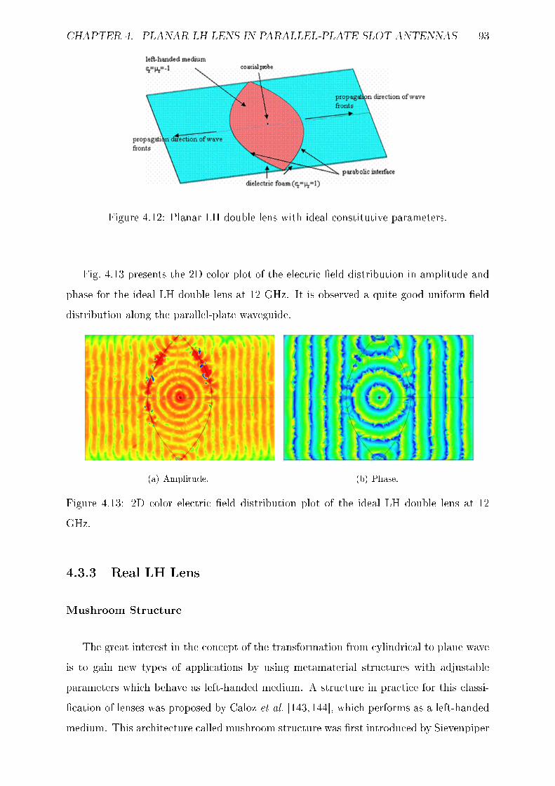
CHAPTER 4. PLANAR LH LENS IN PARALLEL-PLATE SLOT ANTENNAS 93
Figure 4.12: Planar LH double lens with ideal constitutive parameters.
Fig. 4.13 presents the 2D color plot of the electric eld distribution in amplitude andphase for the ideal LH double lens at 12 GHz. It is observed a quite good uniform elddistribution along the parallel-plate waveguide.
(a) Amplitude. (b) Phase.
Figure 4.13: 2D color electric eld distribution plot of the ideal LH double lens at 12GHz.
4.3.3 Real LH Lens
Mushroom Structure
The great interest in the concept of the transformation from cylindrical to plane waveis to gain new types of applications by using metamaterial structures with adjustableparameters which behave as left-handed medium. A structure in practice for this classi-cation of lenses was proposed by Caloz et al. [143,144], which performs as a left-handedmedium. This architecture called mushroom structure was rst introduced by Sievenpiper

CHAPTER 4. PLANAR LH LENS IN PARALLEL-PLATE SLOT ANTENNAS 94
as high-impedance surface, where it was employed, because of its prohibited frequencyband, for instance for suppression of spurious surface waves in planar antennas [3]. In [142]and [138] the mushroom arrangement was veried to be appropriate to present the eect ofa positive/negative refractive index in its pass band gained by adequate designed parame-ters. Thus, it may be an alternative for left-handed media in terms of novel kind of lenses.The mushroom conguration is applied, as it can be seen in Fig. 4.14, for the physicalrealization of the real left-handed planar lens as a form of excitation to feed parallel-plateslot antennas. In Fig. 4.14(a) this texture structure is presented which is composed ofarrays of metallic microstrip patches connected to the ground plane with periodic vias inthe dielectric substrate. To design the mushroom structure, a unit cell is rst analyzed.As shown in Fig. 4.14, the unit cell is design as it is enclosed between two metallic platein a parallel-plate waveguide situation (see Fig. 4.14(a) and Fig. 4.14(b)). The mushroomstructure unit cell is designed over a substrate with εr = 2.17 of thickness h and withan airbox between the two metallic plates as illustrated in Fig. 4.14(c) to reveal a left-handed behavior in the band of 12 GHz. We will see that the thickness t of the metalizedmicrostrip patch play an important role in the LH behavior of the mushroom structures.The characterization of the left handed lens with the mushroom structure in terms of theirgeometrical parameters (lattice constant, diameter of via, height of substrate, thicknessof the patch) is presented using the dispersion diagram of the unit cell.
The parameters of the mushroom structure unit cell are summarized in Table 4.1.
Structure parameterslattice constant or period p
distance between adjacent patches g
metalized via diameter dvia
metalized patch thickness t
Dielectric substratetype NELTEC NY217
dielectric constant εr=2.17dielectric thickness h
Table 4.1: Mushroom structure unit cell parameters.
Other parameters as the ground plane thickness hgnd and the distance hppwg between

CHAPTER 4. PLANAR LH LENS IN PARALLEL-PLATE SLOT ANTENNAS 95
the two PEC plates of the parallel-plate waveguide are dened in Fig. 4.14(c).
(a) Mushroom structure in the real LH lens. (b) Prole view: parallel-plate waveguide withthe real LH lens.
(c) Unit cell of the mushroom struc-ture.
Figure 4.14: Real LH lens with mushroom structures as feeding network of the parallel-plate waveguide.
The mushroom structure with its equivalent circuit is shown in Fig. 4.15. This rep-resentation (Fig. 4.15(b)) is commonly used to realize two-dimensional CRLH metama-terials [11]. The edge coupling between adjacent metal patches contributes to the seriescapacitance CLH , while the via connecting the metal patch to the ground plane providesthe shunt inductance LLH . We will see in the parametric study in 4.3.3, that the seriescapacitance CLH that depends of the patch thickness t of the mushroom, play an impor-

CHAPTER 4. PLANAR LH LENS IN PARALLEL-PLATE SLOT ANTENNAS 96
tant role in the mushroom structure for the LH behavior. Besides these LH contributions,RH parasitic eect also occur with series inductance due to current ow on the metalpatch and shunt capacitance from the voltage gradient between the metal patch and theground plane. In Fig. 4.15(b), the equivalent circuit model of the mushroom structureunit cell consists of a series RH inductance LRH , a series LH capacitance CLH , a shuntRH capacitance CRH and a shunt LH inductance LLH .
(a) Mushroom structure.
C ´/ zLH
D
L ´/ zLH
D
Dz
L ´ zRH
D
C ´ zRH
D
Z´
Y´
(b) Equivalent transmission line model.
Figure 4.15: Mushroom structure transmission line model.
The mushroom structure appears to be a perfectly homogeneous and isotropic struc-ture for electromagnetic (EM) waves, allowing refractive eects, described by simple rayoptics [204]. this means that the EM waves do not see the discontinuities of the periodicstructure when the lattice constant p of the mushroom structure are [11]:
p ¿ λg , (4.19)
at leastp <
λg
4⇒ |β|p <
π
2. (4.20)
with λg is the guided wavelength and β is the propagation constant. If p > λg, the struc-ture becomes anisotropic and starts to experience scattering. Therefore, the mushroomstructures do not have LH behavior.
Dispersion Diagram
The design of the real LH lens with mushroom structure is done using dispersiondiagrams to fully characterize the mushroom structure and conrm its properties as aLH behavior. In particular, the two-dimensional dispersion diagram is used in order toobserve the unit-cell's propagation constant for dierent angles of an incident wave. Such

CHAPTER 4. PLANAR LH LENS IN PARALLEL-PLATE SLOT ANTENNAS 97
diagram describes the propagation characteristics of innitely periodic structures. Thedispersion diagram plots a structure's β versus frequency. Since we are dealing withperiodic structures, only the dispersion diagram for one unit cell is need to characterizethe entire structure. The dispersion diagram for a unit cell of period p, will show thephase-shift (βp) versus frequency. These diagrams present propagating modes and bandgaps that can potentially exist between such modes (in a periodic structure at a givenfrequency of operation, many modes in dierent directions may be excited). Brillouin,in this theory of wave propagation in periodic structures [53, 54], states that for anyperiodic structure there are certain vectors (i.e. directions) in the unit cell of the periodicstructure that constitute a boundary region of propagation called irreducible Brillouinzone. According to this theory, deriving the propagating modes in the direction of thesevectors suces to cover all the possible direction of propagation within the lattice. Hencethe problem of deriving the propagating modes excited at a certain frequency reduces tonding such modes only in the directions of the vectors of the irreducible Brillouin zoneor Brillouin triangle. For the mushroom structure considered here, the irreducible zone orBrillouin triangle is shown above the top plane and illustrated in Fig. 4.16 and it consistof the direction pointing from Γ to X, from X to M and from M back to Γ.
X M
G
fase 1
fase 2
Figure 4.16: Brillouin triangle of the mushroom structure unit cell (top view).
Therefore, in light of Brillouin theory, a dispersion diagram for the mushroom struc-tures (with square patches) will consist of three regions. In each region the wave vectorβ, translated into the phase shift between the sides of the mushroom unit cell shownin Fig. 4.16 is considered. This translation allows the derivation of dispersion diagramusing traditional eigenmode full-wave simulation. The unit cell structure and requiredphase shift (shown as Phase 1 and Phase 2 in Fig. 4.16) are given to the simulator. Thesimulator calculates the frequencies of propagating waves that would generate such phaseshifts. For a wave propagating in the x direction with no variation in the y direction,

CHAPTER 4. PLANAR LH LENS IN PARALLEL-PLATE SLOT ANTENNAS 98
phase 1 varies between 0 and 180 and phase 2 is kept constant at 0. This correspondsto the Γ to X direction. The X to M direction corresponds to phase 1 being constant andequal to 180 and phase 2 varying from 0 and 180. This represents the second region inthe dispersion diagram (see Fig. 4.17(a)). The third region is represented by the M to Γ
direction in which both phase are equal and changing from 180 back to 0. For the caseof wave propagation in a space lled with only dielectric, as there is no dispersion, thediagram will constitute of a straight line in the rst and third region. Equation (4.21)denes the dispersion diagram f -βp for a wave propagating in a free space lled withdielectric as we have in the structure:
f(βp) =
c
2πp(βp) Γ-X ,
c
2πp
√π2 + (βp)2 X−M ,
c√
2
2πp(βp) M−Γ .
(4.21)
where p is the lattice constant or period of the periodic structure and c = c0√εr
is the speedof light in the dielectric. In our case, as the mushroom structure is enclosed in a airboxbetween parallel-plate waveguide, the dielectric considered here is the air (εr=1).
Fig. 4.17(a) shows the typical dispersion diagram of a mushroom structure unit celldened in Fig. 4.14(c). The rst mode or fundamental mode exhibits the expected slope,corresponding to LH behaviour in the Γ − X, M − Γ direction and also X − M direc-tion. The rst higher mode is a TE mode that behaves as LH medium very close theΓ point. The second higher order mode is a RH mode [11]. The dispersion diagram ofFig. 4.17(a) shows that the mushroom structures supports a backward wave (LH mode)at low frequencies and a forward wave (RH mode) at high frequencies. As we can observein Fig. 4.17(b), a phase match occurs between the LH mode of the mushroom structureand the adjacent conventional or RH medium that are in the RH part of the parabolicinterface of the lens (See Fig. 4.14(b)) which correspond with the positive-slope dielectricline. The point, where the phase match (phase matching condition) happens, indicatesthat the magnitude of refractive indices are equal (equivalent electromagnetic densitiesnRH = −nLH). In addition, the Γ−X and Γ−M are almost overlaid to show the isotropicnature of the mushroom structure for phase shifts (βp) less than π
2.

CHAPTER 4. PLANAR LH LENS IN PARALLEL-PLATE SLOT ANTENNAS 99
(a) Dispersion diagram of the mushroom structureunit cell.
(b) Intersection between LH mode of the mushroomstructures and the dielectric line of the RH media:phase matching condition.
Figure 4.17: Dispersion diagram of the mushroom structure unit cell.
Design of the Mushroom Structure Unit Cell
Fig. 4.18(a) represents the real simulation model used to extract the dispersion diagramof the mushroom structure that will be used to design and implement the real planar LHlens.The unit cell model includes a patch printed on a substrate of dielectric constant εr =2.17 and the metal via. In all the simulations that will be done, the ground plane thicknesshgnd is 1 mm and the space hppwg is 8 mm. Applying a periodic boundary condition onthe sides of the unit cell (placed in the x-z and y-z planes) to mimic the presence of thecell in a periodic structure, and a perfect electric conductor (PEC) boundary conditionon the top and bottom of the cell with an airbox between them is shown in Fig. 4.18.First, we have designed a mushroom structure unit cell for εr,LH = -10.2, µr,LH = -1 (nLH
= -3.2) at 12 GHz with the following parameters summarized in Table 4.2.

CHAPTER 4. PLANAR LH LENS IN PARALLEL-PLATE SLOT ANTENNAS 100
Structure dimensionsParameters Value
lattice constant p 3.2 mmdistance between adjacent patches g 0.2 mm
dielectric thickness h 0.762 mmpatch thickness t 0.5 mmvia diameter dvia 0.8 mm
Table 4.2: Mushroom structure unit cell dimensions for εr,LH = -10.2, µr,LH = -1 (nLH =-3.2) at 12 GHz.
(a) Unit cell. (b) detail of the metallic via.
(c) Boundary conditions. (d) Unit cell parameters.
Figure 4.18: Simulation model of the mushroom structure unit cell in CST MicrowaveStudio.
As we will see in the parametric study 4.3.3, the thickness of the patch t and the
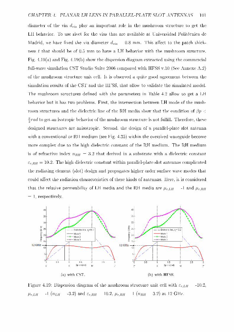
CHAPTER 4. PLANAR LH LENS IN PARALLEL-PLATE SLOT ANTENNAS 101
diameter of the via dvia play an important role in the mushroom structure to get theLH behavior. To use rivet for the vias that are available at Universidad Politécnica deMadrid, we have xed the via diameter dvia = 0.8 mm. This aect to the patch thick-ness t that should be of 0.5 mm to have a LH behavior with the mushroom structure.Fig. 4.19(a) and Fig. 4.19(b) show the dispersion diagram extracted using the commercialfull-wave simulation CST Studio Suite 2006 compared with HFSS v.10 (See Annexe A.2)of the mushroom structure unit cell. It is observed a quite good agreement between thesimulation results of the CST and the HFSS, that allow to validate the simulated model.The mushroom structures dened with the parameters in Table 4.2 allow to get a LHbehavior but it has two problems. First, the intersection between LH mode of the mush-room structures and the dielectric line of the RH media show that the condition of βp <π2rad to get an isotropic behavior of the mushroom structure is not fulll. Therefore, these
designed structures are anisotropic. Second, the design of a parallel-plate slot antennawith a conventional or RH medium (see Fig. 4.35) within the oversized waveguide becomemore complex due to the high dielectric constant of the RH medium. The RH mediumis of refractive index nRH = 3.2 that derived in a substrate with a dielectric constantεr,RH = 10.2. The high dielectric constant within parallel-plate slot antennas complicatedthe radiating element (slot) design and propagates higher order surface wave modes thatcould aect the radiation characteristics of these kinds of antennas. Here, it is consideredthat the relative permeability of LH media and the RH media are µr,LH = -1 and µr,RH
= 1, respectively.
(a) with CST. (b) with HFSS.
Figure 4.19: Dispersion diagram of the mushroom structure unit cell with εr,LH = -10.2,µr,LH = -1 (nLH = -3.2) and εr,RH = 10.2, µr,RH = 1 (nRH = 3.2) at 12 GHz.

CHAPTER 4. PLANAR LH LENS IN PARALLEL-PLATE SLOT ANTENNAS 102
Fig. 4.20 represents the refractive index n of the mushroom structure computed fromthe dispersion diagram results by:
|n(ω)| = cβ(ω)
ω, (4.22)
where c0 is the speed of light in the medium. The sign of n is positive when the structurebehaves as a RH medium (positive slope in the dispersion diagram) and negative when itbehaves as a LH medium (negative slope in the dispersion diagram).
(a) with CST. (b) with HFSS.
Figure 4.20: Refractive index n of the mushroom structure unit cell with nLH = -3.2 at12 GHz.
It is observed the presence of the negative refractive index nLH (LH behavior = LHmode = mode 1) of the mushroom structure in the direction Γ − X and M − Γ of theBrillouin triangle. The problem of the anisotropy can be observed also in Fig. 4.20(a) andFig. 4.20(b). If the structure would be isotropic, the Γ −X and M − Γ of the Brillouintriangle would have an equal magnitude nLH=-3.2 of refractive indices at the same phaseβp less than π
2.
As in Subsection 4.3.2, an ideal LH lens model implemented of a paraboidal refractiveRH/LH matched interface placed between the LH medium (ideal perfectly-homogeneousmedium with the constitutive parameters εr,LH = −2.43 and µr,LH = −1 (nLH = -1.56) and the RH medium (hard commercial polyethylene substrate with the constitutiveparameters εr,RH = 2.25 and µr,RH = 1 (nRH = 1.5) is analyzed at 12 GHz (see Fig. 4.8(a)).Here, the real LH lens implemented with mushroom structure is designed to achieve anegative refractive index nLH = −1.56 as a LH behavior. Therefore, we have implementeda mushroom structure with εr,LH = -2.43, µr,LH = -1 (nLH = -1.56) at 12 GHz as shown

CHAPTER 4. PLANAR LH LENS IN PARALLEL-PLATE SLOT ANTENNAS 103
in Fig. 4.21. The RH medium is of refractive index nRH = 1.5 that derived in a substratewith a dielectric constant εr,RH = 2.25. This substrate denominated polyethylene iscommonly used in the design of parallel-plate slot antennas. The RH and LH mediumsare not completely matched (nRH ≈ −nLH) but the reection due to the mismatch areinsignicant. The dimensions of the mushroom structure with εr,LH = -2.43, µr,LH = -1(nLH = -1.56) working at 12 GHz are summarized in Table 4.3.
Structure dimensionsParameters Value
lattice constant p 3.64 mmdistance between adjacent patches g 0.29 mm
dielectric thickness h 0.3 mmpatch thickness t 0.4 mmvia diameter dvia 0.15 mm
Table 4.3: Mushroom structure unit cell dimensions with εr,LH = -2.43, µr,LH = -1 (nLH
= -1.56) at 12 GHz.
Fig. 4.21(a) shows the dispersion diagram of the mushroom structure unit cell. It isobserved that the mushroom structures dened with the parameters in Table 4.3 allow toget a LH behavior but it has two important fabrication problem. First, the diameter ofthe vias dvia = 0.15 mm are small and it is more complex to manufacture it. Secondly, thepatch thickness t=0.3 mm can not be etched by photolithography technology, available atUniversidad Politécnica de Madrid, but only by laser. These two problems complicatedthe manufacturing of these parameters for the mushroom structures. Fig. 4.22 presentedthe intersection between LH mode of the mushroom structures and the dielectric lineof the RH media show that the condition of βp < π
2rad to get an isotropic behavior of
the mushroom structure is fulll. It is also shown the negative slope which derived in arefractive index nLH (LH behavior = LH mode = mode 1) of the mushroom structurein the direction Γ − X and Γ −M of the Brillouin triangle. The structure is isotropic,because the Γ − X and Γ − M direction of the Brillouin triangle have almost an equalmagnitude nLH=-1.56 of refractive indices at the same phase (phase matching condition)βp less than π
2as presented in Fig. 4.21(b).

CHAPTER 4. PLANAR LH LENS IN PARALLEL-PLATE SLOT ANTENNAS 104
(a) Dispersion diagram. (b) Refractive index n.
Figure 4.21: Mushroom structure unit cell with εr,LH = -2.43, µr,LH = -1 (nLH = 1.56)and εr,RH = 2.25, µr,RH = 1 (nRH = 1.5) at 12 GHz.
Figure 4.22: Dispersion diagram of the mushroom structure unit cell: Phase matchingcondition (isotropy nature).
The mushroom structure for the real LH lens is analyzed at a working frequency of7.5 GHz. As in Subsection 4.3.2 (see Fig. 4.9), an ideal LH lens model implementedof a paraboidal refractive RH/LH matched interface placed between the LH medium(ideal perfectly-homogeneous medium with the constitutive parameters εr,LH = −2.43
and µr,LH = −1 (nLH = -1.56) and the RH medium (hard commercial polyethylenesubstrate with the constitutive parameters εr,RH = 2.25 and µr,RH = 1 (nRH = 1.5) isanalyzed at 7.5 GHz. Here, the real LH lens implemented with mushroom structure isdesigned to achieve a negative refractive index nLH = −1.56 as a LH behavior. Therefore,we have implemented a mushroom structure with εr,LH = -2.43, µr,LH = -1 (nLH = -1.56)at 7.5 GHz as shown in Fig. 4.23. The RH medium is of refractive index nRH = 1.5 that

CHAPTER 4. PLANAR LH LENS IN PARALLEL-PLATE SLOT ANTENNAS 105
derived in a substrate with a dielectric constant εr,RH = 2.25. This substrate denominatedpolyethylene is commonly used in the design of parallel-plate slot antennas. The RH andLH mediums are not completely matched (nRH ≈ −nLH) but the reection due to themismatch are insignicant. The dimensions of the mushroom structure with εr,LH = -2.43,µr,LH = -1 (nLH = 1.56) working at 7.5 GHz are summarized in Table 4.4.
Structure dimensionsParameters Value
lattice constant p 5.8 mmdistance between adjacent patches g 0.2 mm
dielectric thickness h 0.762 mmpatch thickness t 0.5 mmvia diameter dvia 0.8 mm
Table 4.4: Mushroom structure unit cell dimensions with εr,LH = -2.43, µr,LH = -1 (nLH
= 1.56) at 7.5 GHz.
Fig. 4.23(a) shows the dispersion diagram of the mushroom structure unit cell. It isobserved that the mushroom structures dened with the parameters in Table 4.4 allowto get a LH behavior. As we have mentioned before and we will see in the parametricstudy 4.3.3, the thickness of the patch t and the diameter of the via dvia play an importantrole in the mushroom structure to get the LH behavior. To use rivet for the vias that areavailable at Universidad Politécnica de Madrid, we have xed the via diameter dvia = 0.8mm. This aect to the patch thickness t that should be of 0.5 mm to have a LH behaviorwith the mushroom structure. Therefore, the patch thickness t=0.5 mm can not be etchedby photolithography technology, available at Universidad Politécnica de Madrid, but onlyby laser. This fabrication limitation complicated the manufacturing of the real LH lensimplemented with these parameters for the mushroom structures. Fig. 4.24, that presentsthe intersection between LH mode of the mushroom structures and the dielectric line ofthe RH media, shows that the condition of βp < π
2rad to get an isotropic behavior of
the mushroom structure is fulll. It is also shown the negative slope which derived in arefractive index nLH (LH behavior = LH mode = mode 1) of the mushroom structurein the direction Γ − X and Γ −M of the Brillouin triangle. The structure is isotropic,because the Γ − X and Γ − M direction of the Brillouin triangle have almost an equalmagnitude nLH=-1.56 of refractive indices at the same phase (phase matching condition)

CHAPTER 4. PLANAR LH LENS IN PARALLEL-PLATE SLOT ANTENNAS 106
βp less than π2as presented in Fig. 4.23(b).
(a) Dispersion diagram. (b) Refractive index n.
Figure 4.23: Mushroom structure unit cell with εr,LH = -2.43, µr,LH = -1 (nLH = 1.56)and εr,RH = 2.25, µr,RH = 1 (nRH = 1.5) at 7.5 GHz.
Figure 4.24: Dispersion diagram of the mushroom structure unit cell: Phase matchingcondition (isotropy nature).
Parametric Characterization
We now characterize the mushroom structure in terms of its dispersion diagram andrefractive index as a function of their geometrical parameters (lattice constant p, distancebetween adjacent patches g, dielectric thickness h, patch thickness t and via diameter dvia)which are the most signicant parameters. Here, only the rst two modes (LH mode=LHbehavior and TE mode) is plotted in the dispersion diagram. The parametric analysis isdone by simulation with the commercial software CST Studio Suite 2006. Several signi-cant characteristics of the mushroom structure are observed. The characterization is done

CHAPTER 4. PLANAR LH LENS IN PARALLEL-PLATE SLOT ANTENNAS 107
at 12 GHz for the mushroom structure unit cell parameters summarized in Table 4.2. Thecorresponding results presented in Fig. 4.25 - Fig. 4.34 may be used as design guidelines.
Figure 4.25: Eect of the variation of lattice constant p on the dispersion diagram.
(a) Refractive index n in the Γ−X direction.
(b) Refractive index n in the Γ−M direction.
Figure 4.26: Eect of the variation of lattice constant p on the refractive index.

CHAPTER 4. PLANAR LH LENS IN PARALLEL-PLATE SLOT ANTENNAS 108
From Fig. 4.26(a), we observe that when the value of the lattice constant p is increased,the condition of (4.20) is no more fulll, so the mushroom structure is anisotropic.
Figure 4.27: Eect of the variation of distance between adjacent patches g on the disper-sion diagram.
(a) Refractive index n in the Γ−X direction. (b) Refractive index n in the Γ−M direction.
Figure 4.28: Eect of the variation of distance between adjacent patches g on the refractiveindex.

CHAPTER 4. PLANAR LH LENS IN PARALLEL-PLATE SLOT ANTENNAS 109
Figure 4.29: Eect of the variation of dielectric thickness h on the dispersion diagram.
(a) Refractive index n in the Γ−X direction. (b) Refractive index n in the Γ−M direction.
Figure 4.30: Eect of the variation of dielectric thickness h on the refractive index.
Figure 4.31: Eect of the variation of patch thickness t on the dispersion diagram.

CHAPTER 4. PLANAR LH LENS IN PARALLEL-PLATE SLOT ANTENNAS 110
(a) Refractive index n in the Γ−X direction. (b) Refractive index n in the Γ−M direction.
Figure 4.32: Eect of the variation of patch thickness t on the refractive index.
Figure 4.33: Eect of the variation of via diameter dvia on the dispersion diagram.
(a) Refractive index n in the Γ−X direction. (b) Refractive index n in the Γ−M direction.
Figure 4.34: Eect of the variation of via diameter dvia on the refractive index.

CHAPTER 4. PLANAR LH LENS IN PARALLEL-PLATE SLOT ANTENNAS 111
From the parametric full-wave analysis, the appropriate selection of the mushroomstructure geometrical parameters can lead to an isotropic and homogeneous LH mediumdespite the manufacturing constraints seen in 4.3.3. From the dispersion diagram, wecan observe that the working frequency where the mushroom structure behaves as a LHmedium:
decreases when the lattice constant p increases.
increases when the distance between adjacent patches g increases.
decreases when the dielectric thickness h increases.
decreases when the patch thickness t increases.
increases when the via diameter dvia increases.
From the refractive index plots, we can observe that the refractive index of the mushroomstructure in the LH behavior:
becomes less negative and the isotropy nature is maintained when the lattice con-stant p increases.
becomes less negative and the isotropy nature is worst when the distance betweenadjacent patches g increases.
becomes more negative and the isotropy nature is best when the dielectric thicknessh increases.
becomes more negative and the isotropy nature is best when the patch thickness t
increases.
becomes less negative and the isotropy nature is worst when the via diameter dvia
increases.
So, the behavior of the LH medium tends to disappear when the lattice constant p, thedistance between adjacent patches g or the via diameter dvia increase and the dielectricthickness h and the thickness patch t decrease. The slope of the refractive index becomesless negative in the dispersion diagram. These parameters dene the geometrical limita-tions to have an isotropic and homogeneous LH medium with the mushroom structures.

CHAPTER 4. PLANAR LH LENS IN PARALLEL-PLATE SLOT ANTENNAS 112
In terms of bandwidth, the mushroom structure depends of the frequency range where itbehaves as an eective LH medium which is in a narrow bandwidth. During the para-metric analysis, we have seen that the variation of the distance between adjacent patchesg, the patch thickness t and the via diameter dvia alter signicantly the isotropy behav-ior of the mushroom structure. On the other hand, the variation of the lattice constantp does not signicantly change the isotropy behaviour of the mushroom structure. Wehave observed that at low frequency, the isotropic and homogeneous LH medium is easierto implement with the mushroom structure. At high frequency for dierent geometricalparameters, the isotropic and homogeneous LH behavior (negative refractive index) dis-appear and the mushroom structure behaves only as a RH medium. Also, the geometricallimitations becomes more complex due to the manufacturing constraints at high frequen-cies. Therefore, the patch thickness t in the order of conventional thickness (18µm or35µm) are impossible at 12 GHz if we want that the mushroom structure behaves as anisotropic and homogeneous LH medium. This parameter complicated a little bit more thecomplexity of the fabrication for the real LH lens implemented with mushroom structures.
4.4 Antenna Structure
A future antenna prototype will use the excitation circuit of the real left-handed lensmade up by the mushroom structure which have been analyzed and designed in thischapter. The basic conguration of the antenna is a two-plate waveguide with printedslots on the superior plate which are excited by plane wave. The slot array antenna isset up by two metallic parallel-plate which constitute the oversized waveguide. The spacein between is lled with a conventional or RH medium (commercial dielectric material).A planar wave front is established between the two conductors. The plane wave frontcouples with a planar array of resonant slots in the upper part of the waveguide. Toprevent reections produced by the individual slots, the radiating elements are formed bythree slots. The central is of the length close to resonance, the lateral slots are of minorlength of which the function is to diminish the reections of the rst one. In Fig. 4.35, aschematic of the prototype of the parallel plate slot antenna is illustrated exhibiting linearpolarization. The real planar LH lens is excited by a coaxial probe that will generate auniform plane wave front within the feed waveguide as demonstrated in Subsection 4.3.2.We will manufacture two prototype: one working in the 7.5 GHz band and the second

CHAPTER 4. PLANAR LH LENS IN PARALLEL-PLATE SLOT ANTENNAS 113
one in the frequency band of 12 GHz.
Figure 4.35: Parallel-plate slot antenna excited by the planar real LH single lens.
4.5 Conclusion
The design, analysis and characterization of the planar LH lens as a feeding networkto generate a TEM plane wave front in parallel-plate slot antennas have been presented.Two cases have been analyzed to validate the correct behaviour of the LH lens for TEMexcitation: rst, the ideal LH lens that is composed of ideal perfectly-homogeneous mate-rials with eective constitutive parameters at 12 GHz for the rst prototype and 7.5 GHzband for the second prototype is studied in simulation. The results show a regular uniformconversion from cylindrical to plane wave in the center of the parallel-plate waveguide.Therefore, the simulations show that the uniformity of the elds distribution within theoversized guiding waveguide is quite good. The magnitude eld patterns are used to con-rm the negative refraction occurring in the ideal LH lens and the propagation of a TEMexcitation. The second case, the real LH lens implemented with mushroom structures isanalyzed in terms of dispersion diagram for the unit cell. The mushroom structures showproper functioning as an isotropic and homogeneous LH medium in the 12 GHz band.Therefore, these structures can be one possibility to conform and design the real LH lens.

CHAPTER 4. PLANAR LH LENS IN PARALLEL-PLATE SLOT ANTENNAS 114
However, the parametric study in terms of the dispersion diagram as a function of theirgeometrical parameters (lattice constant p, distance between adjacent patches g, dielectricthickness h, patch thickness t and via diameter dvia), which are the most signicant para-meters of the mushroom structure have shown the complexity of this feeding consideringthe limitations of planar fabrication technology available at Universidad Politécnica deMadrid. Two prototypes for the real LH lens are designed: the one working in the 7.5GHz band and the second working in frequency band of 12 GHz. The problem is thatto have a good LH behavior in these frequencies, the patch thickness of the mushroomstructure is of 0.5 mm. This thickness can not be done by photolithography etching. Onepossibility can be to use a laser to etch the patches. Although the mushroom structurehave manufacturing constraints, the results are very promising as new excitation form ofTEM mode for parallel-plate slot antennas. The use of these structures in this kind ofantennas supposes a newness with respect to traditional feeding structures.
As a future work in a medium term, we want to validate the simulation results withthe fabrication of a left-handed lens prototype with mushroom structures manufacturedby laser for the practical application in parallel-plate slot antennas in the range of 7.5GHz band for the rst prototype and in the 12 GHz frequency band for the second proto-type. The prototypes will be validated through analyzing the eld distribution within thewaveguide, the aperture eciency and directivity to dene the radiation characteristicsof these antennas.

Chapter 5
Substrate Integrated ArticialDielectric (SIAD) for Planar MicrostripAntenna Miniaturization
Since their invention in 1960s, microstrip patch antennas have found numerous appli-cations for their simplicity in fabrication, compatibility with planar circuitry, low proleand planar structures, and unidirectional radiation capability. Despite many nice electri-cal and mechanical features of microstrip antennas, their use for a number of applicationsat low frequencies has been limited due to their limited size and bandwidth. Therefore,the interests to nd new engineered substrate to improve the limitations and characteristicof microstrip patch antennas are constantly present in the trend of the communicationsindustry to do smaller size devices, thus, ecient antenna miniaturization is a clear ne-cessity.
In this chapter, a novel substrate integrated articial dielectric (SIAD) for miniatur-ized and enhanced-bandwidth planar microstrip patch antennas is proposed. This SIADis presented as a practical planar realization of a magneto-dielectric substrate and char-acterized as a substrate for microstrip structures. The eective constitutive parameters(εeff ,µeff ) including electric and magnetic losses, are extracted and a parametric analysisis carried out. It is shown numerically and experimentally that the SIAD exhibits ar-ticial magneto-dielectric properties with simultaneously enhanced eective permittivityand permeability over a large frequency band from a given host substrate. Consequently,
115

CHAPTER 5. SIAD FOR MICROSTRIP ANTENNA MINIATURIZATION 116
a substrate of higher eective refractive index is obtained, which allows size reductionin planar components and antennas. The SIAD is a fully integrated structure, which isengineered by repeatable laser drilling and metal plating processes. By proper design, itseective parameters for a given host substrate are estimated to be increasable by up to100% for the permittivity and up to 40% for the permeability, corresponding to a guidedwavelength compression factor of up to 71%. Finally, a SIAD patch antenna with an areareduction of 24.5% (non optimal in terms of size reduction) is demonstrated and discussedin terms of bandwidth, radiation eciency and directivity compared to a purely dielectricsubstrate with the same miniaturization factor (neff=√µeffεeff ) as the SIAD and thehomogeneous host substrate.
5.1 Introduction and Motivation
The microstrip antenna concept was introduced for the rst time by Deschamps [29] in1953, although it was not until principle of the 1970's when this idea is rescued [205] and isdeveloped remarkably by Howell [206], being also used in arrays [207]. Later advances inplanar photoetching techniques have allowed to a remarkable advance in the developmentof the microstrip structures like radiating elements, since they are very low cost and easyto manufacture for the radiating systems developed for mobile communication applica-tions [37], satellite communication systems (DBS) [36] or local area networks (LAN) [38].The microstrip planar antennas are the perfect element to develop diverse arrays congu-rations that allow to implement all type of radiating systems [208]: planar arrays, phasedarrays, conformal antennas in which the dierent array congurations are conformed tocertain mechanical forms (cylindrical, spherical, etc.) [209]. One of the advantages of thepatch is that the feeding network can be placed in the same layer where the patches arelocated. In this case the feeding network is formed by a microstrip network located inthe same substrate of the patches. It implies that the zone of union between the ends ofthe network and the patches are by direct bonding. Two types of feeding networks canbe generated: parallel or series. The series feeding has a worst bandwidth due to thevariation of the phase feeding of the patches, eect that does not so much inuence in theparallel feeding [14]. In the same way, the parallel feeding allows a greater freedom in theelement position in arrays. Series patch arrays [210] are very useful in designs in whicha smaller space is required and can be made according to a progressive or resonant wave

CHAPTER 5. SIAD FOR MICROSTRIP ANTENNA MINIATURIZATION 117
scheme. A series-parallel combination in the feeding network is also possible [211]. In anycase, the microstrip designs present evident advantages as far as their simplicity and easyconstruction. Also, they allow to very high levels of precision in its manufacture thanksto the use of the photoetching. Nevertheless, the patch antennas have some disadvantagesthat should be considered. First, the feeding network by direct contact of microstrip linepresents a very narrow bandwidth. For that reason, solutions have looked for increasingthe thickness of the dielectric. It would also imply that the microstrip line widths wouldbe greater, and therefore could radiate more easily. This is related directly with one ofthe disadvantages of having in the same layer the feeding network and the radiating ele-ments: an appreciable increase in the sidelobe levels of the array and a degradation in thepolarization purity [212]. This problem can be solved using the excitation of patches thatisolate the radiating zone form the feeding network through a ground plane: coaxial probefeed and aperture-coupled feed [213]. With the purpose to increase the radiating elementbandwidth, stacked patches are the solution to generate several resonances [214]. In any-one of reference textbooks for the study of antennas, the principles of antenna analysiscan be found [185], as well as multiple congurations to obtain wider bandwidth [34].However, the main disadvantage that presents the patch arrays with microstrip feedingnetworks is in the high losses that these feed have. This eect becomes specially impor-tant in antennas of high gain, in which the number of patches is high and the distributionnetwork covers a great area. It has bad inuence in the eciency with values around 20%in antennas with gain superior to 30 dB in DBS reception [215]. These characteristics arenot comparable with 60% of eciency for the satellite parabolic reectors. The eectscan be diminished choosing low loss substrates, but it is not sucient.
Microstrip antennas is nowadays one of the most commonly used antenna types. Theyhave many desirable characteristics, such as low prole, light weight, robust design andlow manufacturing cost using the benets of printed circuit board technology, but theirapplications in many systems are limited by their excessive size or too narrow band-width [14,185,213]. Novel approaches must be explored to meet the ever increasing needfor ecient small antennas.
The problem of antenna miniaturization is at least 60 years old and has been exten-sively studied by many authors, e.g. [180, 216, 217]. Early studies have shown that, fora resonant antenna in a non-magnetic environment, bandwidth (BW ) and radiation e-ciency ηr both decrease, as size decreases [218]. This is a fundamental limitation which

CHAPTER 5. SIAD FOR MICROSTRIP ANTENNA MINIATURIZATION 118
holds irrespectively to the antenna architecture.
Over the past decades, the most common approach for miniaturizing patch antennashas been to print them on high permittivity dielectric substrates [219]. However, accord-ing to the fundamental limitations mentioned above, the resulting structures suer fromnarrow bandwidth and low eciency, where the eciency may be further reduced by theexcitation of spurious surface waves which also alter the radiation patterns. Placing theantenna on a magneto-dielectric substrate (in particular µr 6= 1 for the magnetic response)can theoretically mitigate these problems [180, 185, 217], i.e. maintain acceptably largebandwidth and eciency as the antenna is miniaturized, but practical magneto-dielectricsubstrates have not been available so far. This is the reason why, articial magneto-dielectric substrates have recently gained increasing attention [179,181,182,220]. In [179],Hansen et al. show how an ideal magneto-dielectric material, having both variable µ andε, aect the patch antenna performance in terms of physical size and bandwidth. In [220],Yoon et al. conrm these trends. Several implementations of articial magneto-dielectricsubstrates have been reported [221224]. However, these substrates are complex andnon compatible with standard microwave integrated circuits (MIC) and monolithic MIC(MMIC) technology. The substrate integrated articial dielectric (SIAD) structure pro-posed in this work is MIC/MMIC-compatible and may therefore represent viable solutionfor miniaturized antennas.
Articial dielectrics (AD) are structures constituted by a matrix (1D, 2D or 3D) ofmetal inclusions of size and inter-spacing much smaller than the guided wavelength [48].As a consequence, they are eective medias which exhibit macroscopic constitutive para-meters produced by the dipolar responses and subsequent polarizabilities of the inclusions,in the same manner as natural dielectric or magnetic substances exhibit macroscopic pa-rameters resulting from their molecular dipolar responses. Articial dielectrics have along history, which in microwave engineering applications go back to the 1950s and 1960swith the works of Kock, Cohn, Collin and Cheng [156,158,162,163,167,225], which weremostly aimed at providing lightweight lenses for antennas radomes. Due to their vol-umetric nature and complex fabrication, these early articial dielectrics found limitedapplications. In the context of emerging metamaterials [11, 12], novel articial dielec-tric structures in planar congurations are being proposed to manipulate the constitutiveparameters microwave integrated circuit substrates [178, 226, 227]. Recently, the novelsubstrate integrated articial dielectric (SIAD) was introduced as an articial dielectric

CHAPTER 5. SIAD FOR MICROSTRIP ANTENNA MINIATURIZATION 119
with magneto-dielectric properties for planar microwave circuit miniaturization [226,228].This SIAD is a fully integrated structure, which is engineered by repeatable laser drillingand metal plating processes compatible with standard planar MIC/MMIC technologies.
This work discusses rst the fundamental properties of a patch antenna on a magneto-dielectric substrate in terms of bandwidth, radiation eciency and directivity. Then, acomparative study of patch antenna performances on three ideal eective homogeneoussubstrates: a purely dielectric substrate (PDS), a magneto-dielectric substrate (MDS)and a purely magnetic substrate (PMS) is carried out also in terms of its main parameterradiation characteristics. The SIAD microstrip line, its electromagnetic principle of op-eration and a procedure for the extraction of its eective constitutive parameters (εeff ,µeff ), its eective refractive index and characteristic impedance, including electric andmagnetic losses, from the scattering parameters are done. A full-wave parametric analysisis also performed to determine the range of the εeff and µeff values achievable with atypical commercial substrate. The practical miniaturized SIAD microstrip patch antennais presented and compared to the homogeneous substrate and a purely dielectric substratewith the same miniaturization factor (neff =
√µeffεeff ).
5.2 Fundamental Properties of a Patch Antenna on aMagneto-Dielectric Substrate
In this section, the fundamental properties of a microstrip patch antenna on a magneto-dielectric substrate are discussed in terms of bandwidth, radiation eciency and direc-tivity. Fig. 5.1 shows a patch antenna on a homogeneous magneto-dielectric substrateincluding dissipative losses (tan δe=ε
′′eff/ε
′eff and tan δm=µ
′′eff/µ
′eff ).
Figure 5.1: Patch antenna on a homogeneous magneto-dielectric substrate.

CHAPTER 5. SIAD FOR MICROSTRIP ANTENNA MINIATURIZATION 120
5.2.1 Bandwidth
Electromagnetic Approach
A square patch on a lossless substrate with arbitrary εeff and µeff may be analyzed interms of a transmission line model [179,185]. In this model, the antenna is considered as anopen-circuited l = λg/2 = λ0/2
√µε transmission line section loaded at both ends by small
admittances accounting for fringing elds and radiation. At the resonance frequency ofthe patch, the imaginary part of the input admittance vanishes (ImYin=0) and thereforethe edge susceptance B may be omitted, leaving only the radiation conductance Gr. Thetransmission line model of the patch antenna on the lossless substrate is drawn in Fig. 5.2
(a) A microstrip patch an-tenna.
(b) Equivalent lossless transmission line.
Figure 5.2: Microstrip patch antenna on a lossless substrate and its equivalent circuittransmission line model.
The two radiation conductances Gr at both ends of the transmission line may becomputed by a cavity model as [179]:
Gr =1
120π2
∫ π
0
sin2
[πw
λ0
cos θ
]sin3 θdθ
cos2 θ, (5.1)
where w is the patch width. Here, we consider a square patch so w=l=λg/2 =
λ0/2√
µε. This gives the radiation conductance in terms of µeffεeff , which is more mean-ingful:
Gr =1
120π2
∫ π
0
sin2
[π
2√
µεcos θ
]sin3 θdθ
cos2 θ, (5.2)
which may be approximated by:
Gr ≈ 1
40√
µε + 170µε, (5.3)

CHAPTER 5. SIAD FOR MICROSTRIP ANTENNA MINIATURIZATION 121
when µε=1 to 10 [179].
Moreover, the radiation quality factor Qr is related to the radiation conductanceby [216]
Qr =πY0
4Gr
, (5.4)
where the characteristic admittance Y0 is approximately (for a wide microstrip line)given by [229]
Y0 =l√
ε
η0h√
µ
l=λ0
2√
µε=
λ0
2η0µh, (5.5)
where η0=√
µ0/ε0=120π is the free space impedance and h is the dielectric thickness.
The quality factor, bandwidth and eciency are antenna gures-of-merit, which areinterrelated. The total quality factor Q is representative of the antenna losses. Theradiation characteristics of the antenna are related to the bandwidth by the total qualityfactor Q, which is related to Qr. The total quality factor Q is inuenced by all the antennalosses and is, in general, written as [185,230]:
1
Q=
1
Qr
+1
Qd
+1
Qc
+1
Qsw
, (5.6)
where Qr is the radiation quality factor (radiation losses), Qd = 1tan δe+tan δm
is thedielectric losses where tan δe and tan δm are the electric and magnetic losses of the sub-strate, Qc = h
∆is the conduction (ohmic) losses where h is the substrate thickness and ∆
is the skin depth of the conductor and Qsw is the surface wave losses. When the dielectric,conductor and surface wave losses are negligible, we have Qr = Q. The Q is related tothe VSWR = 2 ≈ -10dB bandwidth by
BW =1√2Q
, (5.7)
indicating that a low Q is required for a large BW , whereas the antenna can bematched only in a very narrow bandwidth when the Q is high, as is the case in conventionalsmall antennas [180,216].
Substituting (5.3) and (5.5) into (5.4) and inserting the resulting expression for Q =Qr (when dielectric, conductor and surface wave losses are negligible) into (5.7) nally

CHAPTER 5. SIAD FOR MICROSTRIP ANTENNA MINIATURIZATION 122
yields for the case of very small dielectric and conductive losses
BW =
96
õ
ε
h
λ0√2[4 + 17
√µε]
, (5.8)
It shows that for a given antenna size, determined by the product √µε, BW can bemaximized by maximizing the ratio
√µ/ε [179].
Circuital Approach
As pointed out above, a microstrip patch antenna (Fig. 5.3(a)) may be modeled asan open-circuited λg/2 transmission line section, where the characteristic impedance Zc
and propagation constant γ may both be complex, terminated by small admittances(Fig. 5.3(b)). This transmission line model may be shown to be equivalent to the parallelresonance circuit of Fig. 5.3(c) by identication of the input impedance Zin of the twomodels. Note that this is not a topological equivalence, since the patch is distributed,but a mathematical equivalence. The resulting equivalences between the distributed andlumped parameters are summarized in Table 5.1.
(a) A microstrip patch. (b) λg/2 resonant open-ended lossy transmission line.
(c) Parallel RLC resonant circuit.
Figure 5.3: Equivalent circuit model for the microstrip patch antenna.

CHAPTER 5. SIAD FOR MICROSTRIP ANTENNA MINIATURIZATION 123
The input impedance Zin of an open-circuited line of length l is dened as [231]:
Zin = Zc coth(α + jβl) = Zc1 + j tan(βl) tanh(αl)
tanh(αl) + j tan(βl), (5.9)
assuming that l=λg/2 at resonance ω=ω0 and let ω=ω0+∆ω. Then βl=π+π∆ω
ω0
and so
tan(βl) = tan∆ωπ
ω'∆ωπ
ω0
and tanh(αl)'αl. Using these results in (5.8), it gives
Zin =Zc
αl + j
(∆ωπ
ω0
) , (5.10)
Comparing with the input impedance of a parallel resonant circuit(5.10) suggests thatthe equivalent RLC circuit are dened in the second column of Table 5.1 with Q=ω0RC= π
2αl= β
2αsince l=π/β at resonance.
The input impedance Zin of the parallel RLC resonant circuit is dened as:
Zin =
(1
R+
1
jωL+ jωC
)−1
, (5.11)
Near resonance, the input impedance of (5.9) can be simplied as
1
1 + x' 1− x + ... ,
Letting ω=ω0+∆ω, where ∆ω is small, (5.9) can be rewritten as
Zin '(
1
R+
1−∆ω/ω0
jω0L+ jω0C + j∆ωC
)−1
'(
1
R+ j
∆ω
ω20L
+ j∆ωC
)−1
'(
1
R+ 2j∆ωC
)−1
' R
1 + 2j∆=
R
1 + 2jQ∆ω/ω0
, (5.12)

CHAPTER 5. SIAD FOR MICROSTRIP ANTENNA MINIATURIZATION 124
Lumped equivalent Lumped equivalentDistributed (TL) parameters parameters
parameters as a function of as a function ofZc and ω0 from [231] µeff and εeff
ω0 =π
l√
µeffεeff
ω0 =1√LC
ω0 =π
l√
µeffεeff
Zc = Zcr + jZci C =π
2ω0Zc
C =π
2ω0η0
√εeff
µeff
= η0
õeff
εeff
γ = α + jβ L = 1
ω20C
L =2η0
ω0π
õeff
εeff
= 2π
λg
= ω0
c0
√µeffεeff
R = Zc
αlR = η0
αl
õeff
εeff
Table 5.1: Equivalence between distributed and lumped parameters for a patch antennal = λg/2.
The electric and magnetic stored energies for the parallel resonant circuit are givenby:
We =1
4|V |2C , (5.13)
Wm =1
4|V |2 1
ω20L
, (5.14)
leading to a total stored energy of
WT = Wm + We , (5.15)
The radiation quality factor Qr of a planar aperture dened as the ratio of the productof the resonance frequency and the total stored energy to the radiated power [232].
Qr = ω0WT
Prad
= ω0Wm + We
Prad
, (5.16)
Substitution of (5.13) and (5.14) into this formula shows that, for a given radiatedpower (i.e. given resistance value R in the parallel resonant circuit), the quality factoris reduced, and hence the bandwidth is increased, by decreasing C and increasing L.According to the third column of Table 5.1, this is equivalent to increasing
√µeff/εeff in
agreement with the electromagnetic expression (5.8)
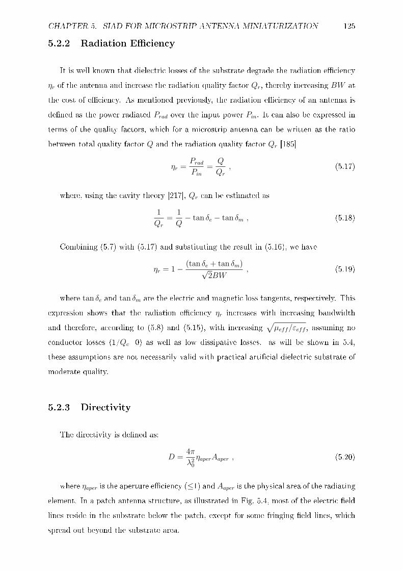
CHAPTER 5. SIAD FOR MICROSTRIP ANTENNA MINIATURIZATION 125
5.2.2 Radiation Eciency
It is well known that dielectric losses of the substrate degrade the radiation eciencyηr of the antenna and increase the radiation quality factor Qr, thereby increasing BW atthe cost of eciency. As mentioned previously, the radiation eciency of an antenna isdened as the power radiated Prad over the input power Pin. It can also be expressed interms of the quality factors, which for a microstrip antenna can be written as the ratiobetween total quality factor Q and the radiation quality factor Qr [185]
ηr =Prad
Pin
=Q
Qr
, (5.17)
where, using the cavity theory [217], Qr can be estimated as
1
Qr
=1
Q− tan δe − tan δm , (5.18)
Combining (5.7) with (5.17) and substituting the result in (5.16), we have
ηr = 1− (tan δe + tan δm)√2BW
, (5.19)
where tan δe and tan δm are the electric and magnetic loss tangents, respectively. Thisexpression shows that the radiation eciency ηr increases with increasing bandwidthand therefore, according to (5.8) and (5.15), with increasing
√µeff/εeff , assuming no
conductor losses (1/Qc=0) as well as low dissipative losses. as will be shown in 5.4,these assumptions are not necessarily valid with practical articial dielectric substrate ofmoderate quality.
5.2.3 Directivity
The directivity is dened as:
D =4π
λ20
ηaperAaper , (5.20)
where ηaper is the aperture eciency (≤1) and Aaper is the physical area of the radiatingelement. In a patch antenna structure, as illustrated in Fig. 5.4, most of the electric eldlines reside in the substrate below the patch, except for some fringing eld lines, whichspread out beyond the substrate area.

CHAPTER 5. SIAD FOR MICROSTRIP ANTENNA MINIATURIZATION 126
(a) Top view: microstrip patch with thefringing elds.
(b) Prole view: electric eld distribution lines.
Figure 5.4: Microstrip patch antenna cavity model considering the fringing elds.
These fringing elds increase the eective patch length beyond its physical length andthereby increase the directivity via ηaper. The eective length of the patch leff is [185].
leff = l + 2∆l , (5.21)
For a given resonance frequency, the length of the patch is
l =λg
2, (5.22)
The dimensions of the patch along its length have been extended on each end by a distance∆l, which is given by Hammerstad [233]as:
∆l = 0.412h(εeff + 0.3)
(w
h+ 0.264
)
(εeff − 0.258)(w
h+ 0.8
) , (5.23)
From these relations, it clearly appears that directivity is reduced when the permit-tivity of the substrate is decreased.
5.2.4 Summary
Fig. 5.5 shows a ow chart summarizing the eects of variation of the eective para-meters µeff and εeff on the fundamental patch antenna performances, resonant qualityfactor Q, bandwidth (BW ) and the radiation eciency ηr, for a magneto-dielectric sub-strate. For a given √µeffεeff (given physical size), the bandwidth and eciency of the

CHAPTER 5. SIAD FOR MICROSTRIP ANTENNA MINIATURIZATION 127
magneto-dielectric antenna are both increased by increasing the ratio√
µeff/εeff , fora given amount of xed and low substrate loss. However, according to (5.22), such anincrease in
√µeff/εeff decreases the directivity of the antenna.
Figure 5.5: Flow chart summary summarizing the eects of the variations of patch antennaperformances as a function of the variations of the magneto-dielectric substrate eectiveparameters.
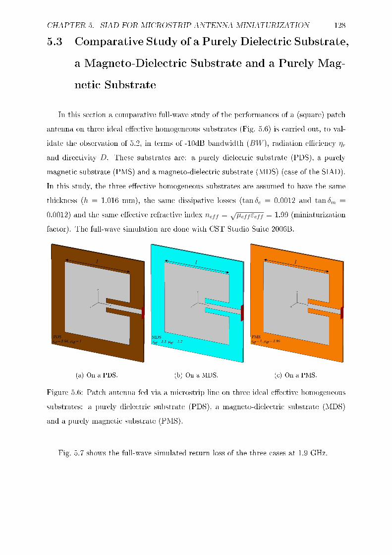
CHAPTER 5. SIAD FOR MICROSTRIP ANTENNA MINIATURIZATION 128
5.3 Comparative Study of a Purely Dielectric Substrate,a Magneto-Dielectric Substrate and a Purely Mag-netic Substrate
In this section a comparative full-wave study of the performances of a (square) patchantenna on three ideal eective homogeneous substrates (Fig. 5.6) is carried out, to val-idate the observation of 5.2, in terms of -10dB bandwidth (BW ), radiation eciency ηr
and directivity D. These substrates are: a purely dielectric substrate (PDS), a purelymagnetic substrate (PMS) and a magneto-dielectric substrate (MDS) (case of the SIAD).In this study, the three eective homogeneous substrates are assumed to have the samethickness (h = 1.016 mm), the same dissipative losses (tan δe = 0.0012 and tan δm =0.0012) and the same eective refractive index neff = √
µeffεeff = 1.99 (miniaturizationfactor). The full-wave simulation are done with CST Studio Suite 2006B.
(a) On a PDS. (b) On a MDS. (c) On a PMS.
Figure 5.6: Patch antenna fed via a microstrip line on three ideal eective homogeneoussubstrates: a purely dielectric substrate (PDS), a magneto-dielectric substrate (MDS)and a purely magnetic substrate (PMS).
Fig. 5.7 shows the full-wave simulated return loss of the three cases at 1.9 GHz.

CHAPTER 5. SIAD FOR MICROSTRIP ANTENNA MINIATURIZATION 129
Figure 5.7: Full-wave simulated return loss of the square patch antenna on a magneto-dielectric substrate with the same eective parameters of the SIAD (εeff = 3.3, µeff =1.2) in comparison with a purely dielectric substrate (εeff = 3.96, µeff = 1) and a purelymagnetic substrate (εeff = 1, µeff = 3.96) with all the same eective refractive index andthe same dissipative losses operating at 1.9 GHz.
Table 5.2 compares the parameters and performances for the microstrip patch antennaon these three substrates. The values in brackets are the results for BW and ηr obtainedby approximate (5.8) and (5.18), respectively.
Purely dielectric Magneto-dielectric Purely magnetic1.9 GHz substrate (PDS) substrate (MDS) substrate (PMS)
(εeff = 3.96, µeff = 1) (εeff = 3.3, µeff = 1.2) (εeff = 1, µeff = 3.96)
Patch size l = 41.5mmneff 1.99√
µeff
εeff0.50 0.60 1.99
-10dB BW 0.52% (0.58) 0.7% (0.69) 1.9% (2.3)ηr 84% (70) 89% (75) 96% (93)D 5.9 dB 5.8 dB 5.3 dB
Table 5.2: Full-wave comparisons of the performances of a square patch antenna of xedsize on a PDS, a MDS and a PMS.

CHAPTER 5. SIAD FOR MICROSTRIP ANTENNA MINIATURIZATION 130
All the trends discussed in 5.2, and summarized in 5.2.4, are veried in the full-waveresults (Table 5.2). The approximate formula (5.8) for BW is very close to the full-waveresults, while the approximate formula (5.18) for ηr, although verifying the expectedtrends, signicantly under-estimate the actual values. The bandwidth of the PMS isstrikingly larger than that of the MDS, which is itself slightly larger than that of thePDS. This may be explained by considering the BW -determinant ratios
√µeff/εeff , for
the PMS, the MDS and the PDS of 1.99, 0.60 and 0.50, respectively (1.990.60.5).
The characteristic impedance of the inset fed microstrip line is specied in Table 5.3
Purely dielectric Magneto-dielectric Purely magneticsubstrate (PDS) substrate (MDS) substrate (PMS)
(εeff = 3.96, µeff = 1) (εeff = 3.3, µeff = 1.2) (εeff = 1, µeff = 3.96)
width 2.54mmZc 49.1Ω 50Ω 172.9Ω
Table 5.3: Characteristic impedance Zc of the inset fed microstrip line.
Fig. 5.8(a), Fig. 5.8(b) and Fig. 5.8(c) show the electric eld distribution for the PDS,MDS and PMS, respectively.
(a) Top view: E-eld distributionof the patch antenna on the PDS.
(b) Top view: E-eld distributionof the patch antenna on the MDS.
(c) Top view: E-eld distributionof the patch antenna on the PMS.
Figure 5.8: Aperture E-eld distribution of the square patch antenna on the three idealhomogeneous substrates: PDS, MDS, PMS.
The eld distribution for the extreme PDS, MDS and PMS clearly show the smallereective aperture responsible for lower directivity in the latter case.

CHAPTER 5. SIAD FOR MICROSTRIP ANTENNA MINIATURIZATION 131
5.4 Substrate Integrated Articial Dielectric (SIAD)Microstrip Transmission Line
5.4.1 Description and Implementation of the Structure
Fig. 5.9(a) shows a microstrip transmission line (TL) printed on a substrate integratedarticial (SIAD). This SIAD is constituted of a dense 2D mesh of metallic wires embeddedin a conventional homogeneous commercial substrate. The metallic wires are copper plat-ted via holes with spacing much smaller than the guided wavelength λg. The vias in theSIAD act as reactive loadings which are designed in terms of their geometrical parameters(lattice constant p, diameter d, height h1 + h2, metal plating thickness) to achieve variouseective permittivity εeff and permeability µeff values. The SIAD structure is planar,and it is entirely integrated in the sense that the SIAD is engineered by standard andrepeatable laser-drilling and electroplating processes, while its assembly with the isolatingprinted substrate is performed via conventional multilayer printed circuit board processes.
(a) Perspective view with detail of a via hole.
(b) Cross section view of the structure.
Figure 5.9: Substrate integrated articial dielectric (SIAD) microstrip transmission lineillustration.
The fabricated SIAD prototype is shown in Fig. 5.10. The host substrate is RT/Duroid

CHAPTER 5. SIAD FOR MICROSTRIP ANTENNA MINIATURIZATION 132
6002 with dielectric constant εr of 2.94, loss tangent tan δe of 0.0012 and thickness h2 of0.508 mm. The wire mesh is made of copper plated via holes having diameter d of0.381 mm using a laser-drilling and holes plating technology available at the Poly-GramesResearch Center in École Polytechnique de Montréal. The vias lattice constant(center-to-center spacing between adjacent via holes) p is 0.635 mm. The via holes have a diameterd of 0.381 mm. The metal plating via hole is an annular structure of 0.0254 mm thicknessand A is the annular metal surface of the via holes. The SIAD contains an array of 200 x200 via holes in the yz plane. The backplane of the SIAD is also copper plated to createa ground plane. The via holes are connected to the ground plane. A thin substrate layeris placed between the TL and the SIAD in order to isolate them, as shown in Fig. 5.9(b).The thin isolating substrate is also RT/Duroid 6002 with thickness h1 of 0.508 mm. Theeective permittivity is εeff = 2.37 for a regular substrate having a thickness h=h1 + h2
= 1.016 mm and εr=2.94.
A system device to avoid the need of glue and soldering the circuits above the SIAD isdeveloped, because the realization of the SIAD at École Polytechnique de Montréal waslimited by the substrate material stock and the time consuming fabrication of the SIAD.Therefore, this device was done to reuse the SIAD and place above it dierent circuits asa microstrip TL line, a microstrip stepped-impedance low-pass lter, a microstrip branch-line coupler or a patch antenna. The SIAD is placed on the air pumped housing deviceshown in Fig. 5.10(a), Fig. 5.10(c) and Fig. 5.10(e). As shown in Fig. 5.10(f), a microstrip50 Ω TL with a width W = 2.54 mm (100 mil) and a length l = 48 mm is etched onthe isolation layer. As mentioned above, this substrate layer is necessary to prevent shortcircuiting the TL and the SIAD grounded via holes.

CHAPTER 5. SIAD FOR MICROSTRIP ANTENNA MINIATURIZATION 133
(a) SIAD on the air pumped housing device. (b) Top view: SIAD with the air pumped hous-ing device.
(c) Top view: air pumped housing device + SIAD. (d) Top view: via holes details.
(e) Substrate integrated articial di-electric (SIAD).
(f) Top view of a microstrip 50Ω TL printed in theisolation layer placed above the SIAD.
Figure 5.10: SIAD prototype.
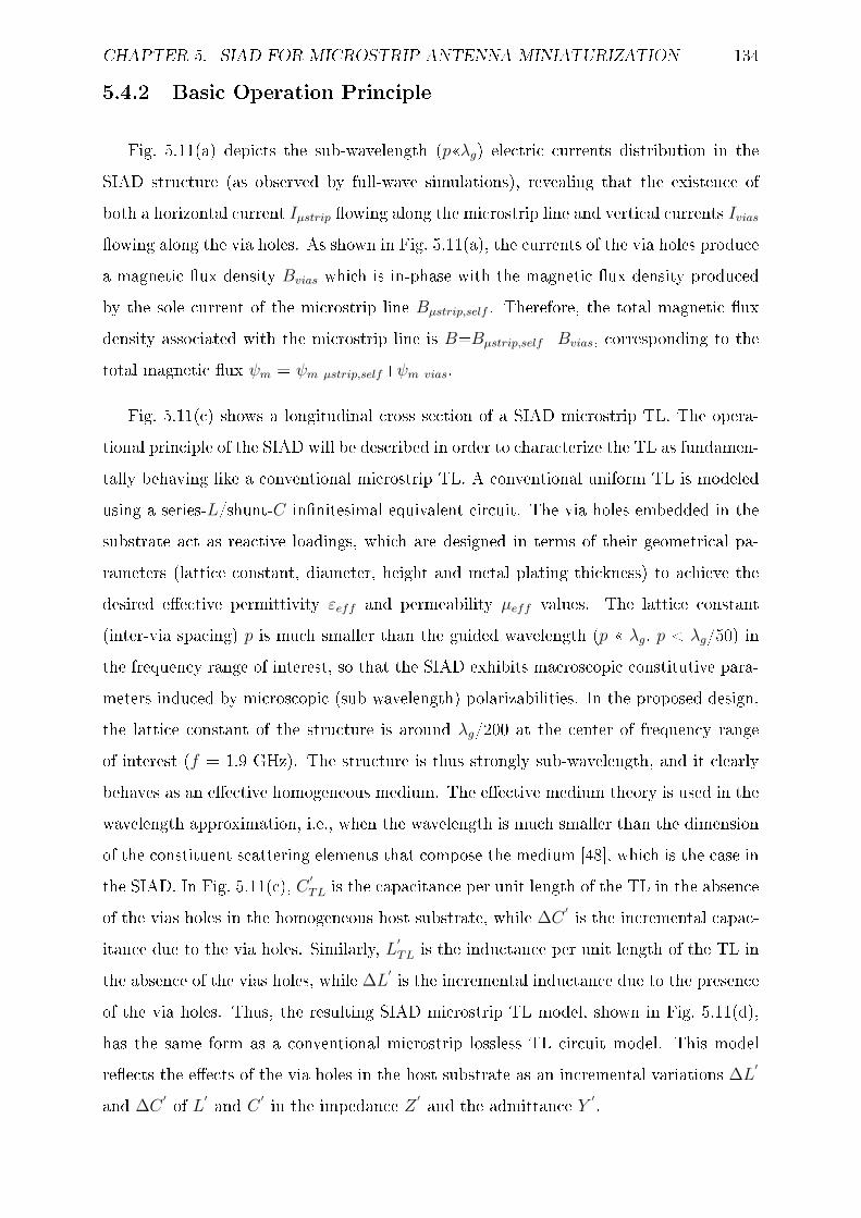
CHAPTER 5. SIAD FOR MICROSTRIP ANTENNA MINIATURIZATION 134
5.4.2 Basic Operation Principle
Fig. 5.11(a) depicts the sub-wavelength (pλg) electric currents distribution in theSIAD structure (as observed by full-wave simulations), revealing that the existence ofboth a horizontal current Iµstrip owing along the microstrip line and vertical currents Ivias
owing along the via holes. As shown in Fig. 5.11(a), the currents of the via holes producea magnetic ux density Bvias which is in-phase with the magnetic ux density producedby the sole current of the microstrip line Bµstrip,self . Therefore, the total magnetic uxdensity associated with the microstrip line is B=Bµstrip,self+Bvias, corresponding to thetotal magnetic ux ψm = ψm µstrip,self+ψm vias.
Fig. 5.11(c) shows a longitudinal cross section of a SIAD microstrip TL. The opera-tional principle of the SIAD will be described in order to characterize the TL as fundamen-tally behaving like a conventional microstrip TL. A conventional uniform TL is modeledusing a series-L/shunt-C innitesimal equivalent circuit. The via holes embedded in thesubstrate act as reactive loadings, which are designed in terms of their geometrical pa-rameters (lattice constant, diameter, height and metal plating thickness) to achieve thedesired eective permittivity εeff and permeability µeff values. The lattice constant(inter-via spacing) p is much smaller than the guided wavelength (p λg, p < λg/50) inthe frequency range of interest, so that the SIAD exhibits macroscopic constitutive para-meters induced by microscopic (sub-wavelength) polarizabilities. In the proposed design,the lattice constant of the structure is around λg/200 at the center of frequency rangeof interest (f = 1.9 GHz). The structure is thus strongly sub-wavelength, and it clearlybehaves as an eective homogeneous medium. The eective medium theory is used in thewavelength approximation, i.e., when the wavelength is much smaller than the dimensionof the constituent scattering elements that compose the medium [48], which is the case inthe SIAD. In Fig. 5.11(c), C
′TL is the capacitance per unit length of the TL in the absence
of the vias holes in the homogeneous host substrate, while ∆C′ is the incremental capac-
itance due to the via holes. Similarly, L′TL is the inductance per unit length of the TL in
the absence of the vias holes, while ∆L′ is the incremental inductance due to the presence
of the via holes. Thus, the resulting SIAD microstrip TL model, shown in Fig. 5.11(d),has the same form as a conventional microstrip lossless TL circuit model. This modelreects the eects of the via holes in the host substrate as an incremental variations ∆L
′
and ∆C′ of L
′ and C′ in the impedance Z
′ and the admittance Y′ .
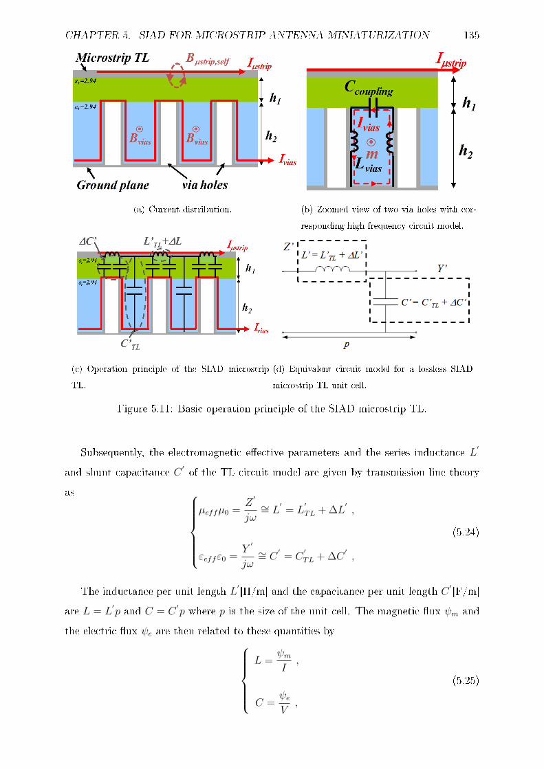
CHAPTER 5. SIAD FOR MICROSTRIP ANTENNA MINIATURIZATION 135
(a) Current distribution. (b) Zoomed view of two via holes with cor-responding high frequency circuit model.
(c) Operation principle of the SIAD microstripTL.
(d) Equivalent circuit model for a lossless SIADmicrostrip TL unit cell.
Figure 5.11: Basic operation principle of the SIAD microstrip TL.
Subsequently, the electromagnetic eective parameters and the series inductance L′
and shunt capacitance C′ of the TL circuit model are given by transmission line theory
as
µeffµ0 =Z′
jω∼= L
′= L
′TL + ∆L
′,
εeffε0 =Y′
jω∼= C
′= C
′TL + ∆C
′,
(5.24)
The inductance per unit length L′ [H/m] and the capacitance per unit length C
′ [F/m]are L = L
′p and C = C
′p where p is the size of the unit cell. The magnetic ux ψm and
the electric ux ψe are then related to these quantities by
L =ψm
I,
C =ψe
V,
(5.25)

CHAPTER 5. SIAD FOR MICROSTRIP ANTENNA MINIATURIZATION 136
The inductance L in (5.24) is directly related to current I. In Fig. 5.11(c), the SIADmicrostrip line carries less current than a similar line on a (via-less) host substrate. Thisis because part of it ows in the vias so that Iµstrip = I-Ivias. Naturally, it follows from(5.24) that the transmission line equivalent inductance L has been enhanced in the SIADcase, i.e. LSIAD=ψm/Iµstrip > ψm/I=Lconventional. Thus, the total inductance per unitlength has been increased to L
′ = L′TL + ∆L
′ , as illustrated in Fig. 5.11(c). In terms ofeective constitutive parameters, this corresponds to an increased eective permeabilitycompared to that of the host medium, i.e. µeff = L
′/µ0 = µhost + ∆µeff . The constitutiveparameter enhancement ∆µeff is related to the geometrical parameters such as diameter,height and metal plating thickness (Fig. 5.9) by the approximate formula
∆L′p = µeffµ0
h2p
d−→ ∆µeff =
h2
d, (5.26)
Alternatively, at high frequencies, the currents owing in the via holes can be viewedas current loops. These current loops generate equivalent magnetic dipole moments m.The equivalent permeability of a metamaterial conguration constituted of periodic res-onant loop circuits embedded in a homogeneous dielectric with intrinsic permeability µ0
considering the general lorentzian type dispersion law and low loss contribution is of theform µeff (ω) = [1+((µs − 1)ω2
r)/(ω2r -ω2))], where µs is the static Reµeff of the SIAD,
ωr is the loop or plasmonic resonant frequency given as ωr = 1/√
2LviaCcoupling. Since thepresence of the coupling capacitance Ccoupling between via holes, ωr is much higher thanthe operating frequency range of the proposed SIAD structure. In this range (ωωr), thepermeability is approximately as µeff (ω) = µs.
In parallel, the capacitance C in (5.24) is directly related to voltage V . Comparedto the conventional microstrip line, the SIAD microstrip line structure exhibits a highertransmission line equivalent capacitance due to the increased capacitance between thetrace and the metallic annular surface at the top of the via holes, i.e. CSIAD = ψe/V∆C
> ψe/V = Cconventional. The total capacitance has thus been increased to C′ = C
′TL +
∆C′ , as illustrated in Fig. 5.11(c). In terms of eective constitutive parameters, this
corresponds to an increased eective permittivity compared to that of the host mediumεeff = C
′/ε0 = εhost + ∆εeff . The constitutive parameter enhancement ∆εeff is relatedto the geometrical parameters such as lattice constant, diameter, height and metal platingthickness (Fig. 5.9) by the approximate formula
∆C′p = εeffε0
A
h1
−→ ∆εeff =A
ph1
, (5.27)
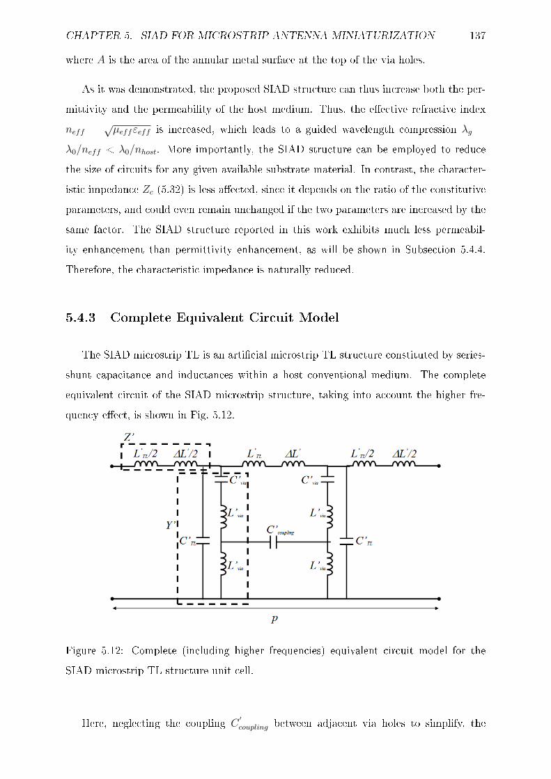
CHAPTER 5. SIAD FOR MICROSTRIP ANTENNA MINIATURIZATION 137
where A is the area of the annular metal surface at the top of the via holes.
As it was demonstrated, the proposed SIAD structure can thus increase both the per-mittivity and the permeability of the host medium. Thus, the eective refractive indexneff = √
µeffεeff is increased, which leads to a guided wavelength compression λg =λ0/neff < λ0/nhost. More importantly, the SIAD structure can be employed to reducethe size of circuits for any given available substrate material. In contrast, the character-istic impedance Zc (5.32) is less aected, since it depends on the ratio of the constitutiveparameters, and could even remain unchanged if the two parameters are increased by thesame factor. The SIAD structure reported in this work exhibits much less permeabil-ity enhancement than permittivity enhancement, as will be shown in Subsection 5.4.4.Therefore, the characteristic impedance is naturally reduced.
5.4.3 Complete Equivalent Circuit Model
The SIAD microstrip TL is an articial microstrip TL structure constituted by series-shunt capacitance and inductances within a host conventional medium. The completeequivalent circuit of the SIAD microstrip structure, taking into account the higher fre-quency eect, is shown in Fig. 5.12.
Figure 5.12: Complete (including higher frequencies) equivalent circuit model for theSIAD microstrip TL structure unit cell.
Here, neglecting the coupling C′coupling between adjacent via holes to simplify, the

CHAPTER 5. SIAD FOR MICROSTRIP ANTENNA MINIATURIZATION 138
equivalent per-unit-length impedance Z′ and admittance Y
′ are:
Z′=jω
(L′TL + ∆L
′
2
),
Y′=jωC
′TL +
jωC′via
1− ω22L′viaC
′via︸ ︷︷ ︸
jω∆C′
,(5.28)
The complete equivalent LC circuit model is next validated by comparison of themeasured and simulated scattering parameters.
The values of the complete equivalent circuit model for ADS circuit model are sum-marized in Table 5.4.
Parameters ValuesLTL 0.22 nH∆L 0.127 nHLvia 0.08 nHCTL 0.09 pFCvia 0.0008 pF
Ccoupling 0.27 pF
Table 5.4: Complete equivalent circuit model parameters.
Fig. 5.13(a) and Fig. 5.13(b) shows the model unit cell for the simulation in CSTStudio Suite 2006B and ANSOFT's High Frequency Structure Simulator (HFSS) tools.Fig. 5.13(c) illustrates the S-parameters results. This comparison allows to validate thecomplete equivalent circuit model dene in Fig. 5.12. The obtained results are quite ingood agreement between the simulator tools results and the dened circuit model andconrm the correct complete equivalent circuit model.

CHAPTER 5. SIAD FOR MICROSTRIP ANTENNA MINIATURIZATION 139
(a) CST unit cell model. (b) HFSS unit cell model.
0 5 10 15 20−30
−25
−20
−15
−10
−5
0
Frequency [GHz]
Mag
nitu
de [d
B]
ADS complete equivalent circuit modelCST Microwave Studio modelHFSS model
(c) S-parameters results: S11 (solid line) and S21 (dashedline).
Figure 5.13: S-parameters of SIAD microstrip TL structure unit cell model.
Another comparison to validate the ADS circuit model with more cells, are done withCST model with 30 cells long. The obtained results in the two case are in good agreement.Fig. 5.14(a) and Fig. 5.14(b) show the CST Microwave Studio model with for 30 cells long.

CHAPTER 5. SIAD FOR MICROSTRIP ANTENNA MINIATURIZATION 140
(a) Perspective view of CST model for 30 cellslong.
(b) CST model structure for 30 cells long.
0 5 10 15 20−30
−25
−20
−15
−10
−5
0
Frequency [GHz]
Mag
nitu
de [d
B]
CST Microwave Studio model: 30 cellsADS complete equivalent circuit model: 30 cells
(c) S-parameters results: S11 (solid line) and S21 (dashedline).
Figure 5.14: S-parameters of SIAD microstrip TL structure for 30 cells long: comparisonADS circuit model and CST model.
5.4.4 S-Parameters
The measured scattering parameters of the SIAD microstrip 50Ω TL prototype shownin Fig. 5.10(f) are compared to those of a microstrip 50Ω TL on a regular RT/Duroid6002 substrate with the same substrate thickness (h = h1+h2 = 1.016 mm) and the SIADmicrostrip TL complete equivalent circuit model in the frequency range from DC to 20GHz. The results are shown in Fig. 5.15.

CHAPTER 5. SIAD FOR MICROSTRIP ANTENNA MINIATURIZATION 141
(a) Magnitude. (b) Unwrapped phase.
Figure 5.15: S-parameters for the SIAD 50Ω TL compared to those of a 50Ω TL on aregular RT/Duroid 6002 substrate and the SIAD TL equivalent circuit model.
As shown in Fig. 5.15(a), good matching and low insertion losses (0.1 to 0.7 dB until4 GHz) throughout the simulated and measured scattering parameters over the frequencyrange are achieved. It may be seen for the larger phase shift (Fig. 5.15(b)), that thepropagation constant β in the SIAD structure has been increased in comparison to itsvalue in the regular RT/Duroid 6002 substrate. This indicates that the SIAD has ahigher eective refractive index neff or, equivalently, exhibits slow-wave characteristics.Good agreement is also observed between the results given by the complete equivalentLC circuit model and the measurements in comparison with the conventional microstripTL on a regular RT/Duroid 6002 substrate.
Fig. 5.16 shows the experimental setup used to measure the S-parameters.
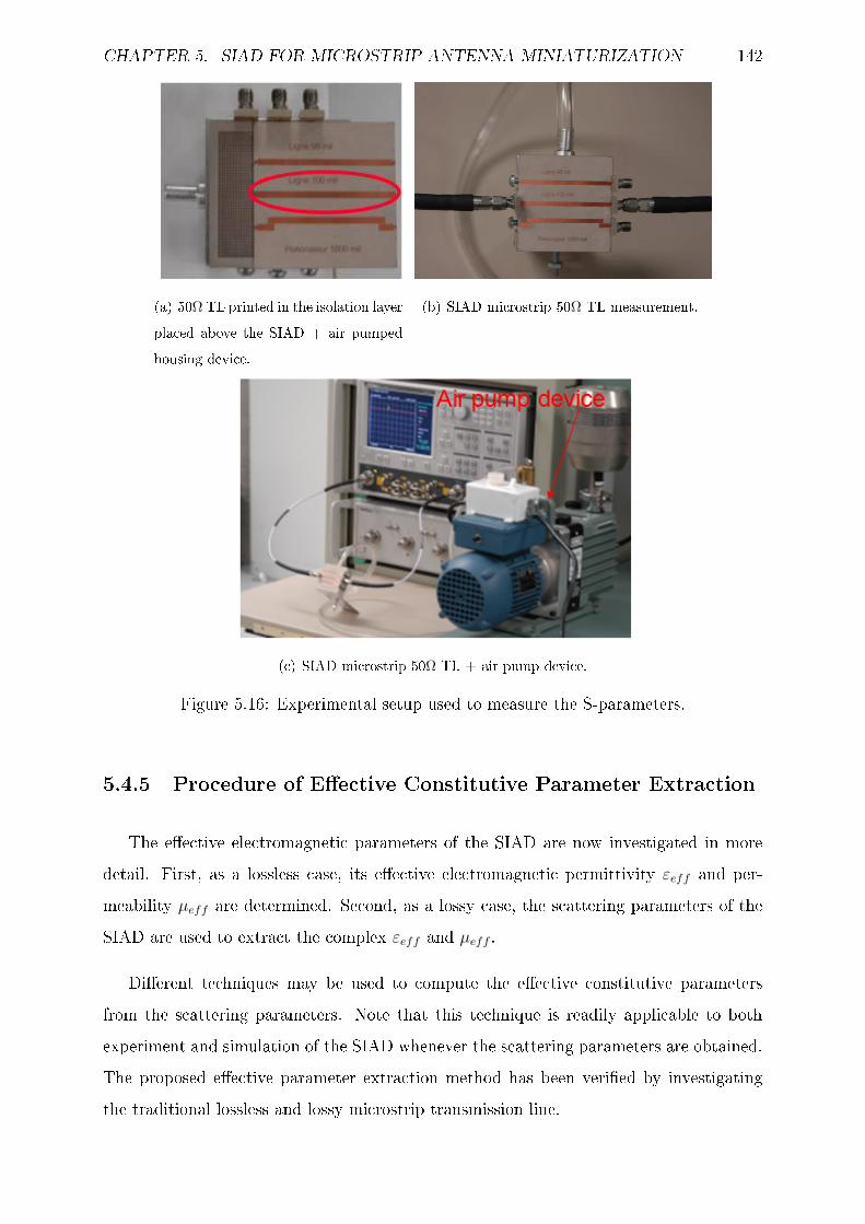
CHAPTER 5. SIAD FOR MICROSTRIP ANTENNA MINIATURIZATION 142
(a) 50Ω TL printed in the isolation layerplaced above the SIAD + air pumpedhousing device.
(b) SIAD microstrip 50Ω TL measurement.
(c) SIAD microstrip 50Ω TL + air pump device.
Figure 5.16: Experimental setup used to measure the S-parameters.
5.4.5 Procedure of Eective Constitutive Parameter Extraction
The eective electromagnetic parameters of the SIAD are now investigated in moredetail. First, as a lossless case, its eective electromagnetic permittivity εeff and per-meability µeff are determined. Second, as a lossy case, the scattering parameters of theSIAD are used to extract the complex εeff and µeff .
Dierent techniques may be used to compute the eective constitutive parametersfrom the scattering parameters. Note that this technique is readily applicable to bothexperiment and simulation of the SIAD whenever the scattering parameters are obtained.The proposed eective parameter extraction method has been veried by investigatingthe traditional lossless and lossy microstrip transmission line.

CHAPTER 5. SIAD FOR MICROSTRIP ANTENNA MINIATURIZATION 143
Lossless case: α = 0 ⇒ γ = jβ
In this section, it is considered the case of small losses, the real parts of these pa-rameters are not aected by losses [231], and we will therefore neglect them here. Thelossless transmission line parameters of the microstrip SIAD structure are extracted tocompute its eective parameters εeff and µeff . Since the SIAD medium is eective, thequasi-TEM nature of the microstrip TL on it is perfectly preserved. Fig. 5.17 shows thetraditional lossless TL circuit model.
Figure 5.17: Traditional lossless TL circuit model.
The propagation constant β and input impedance Zin of a TL are well known [231]and given by
β = −θ
l= −unwrapped[phase(S21)]
l, (5.29)
Zin = ZcZL + jZctan(βl)
Zc + jZLtan(βl), (5.30)
Γ = |S11| = Zin(Zc, β)− Zg
Zin(Zc, β) + Zg
, (5.31)
where l is the length of the transmission line, ZL = 50 Ω is the load impedance, Zin isthe input impedance, Zc is the characteristic impedance of the TL and Zg is the generatorimpedance. By combining (5.29), (5.30) and (5.31), and using the measured S-parameters,the eective propagation constant β and characteristic impedance Zc of the SIAD TL canbe readily obtained. The propagation constant β can also be expressed as a function ofthe host medium parameters and the free space wave number k0 as
β = neffk0 =√
εeffµeffk0 , (5.32)

CHAPTER 5. SIAD FOR MICROSTRIP ANTENNA MINIATURIZATION 144
In the most general case of a magnetic-dielectric substrate, the formula for the conven-tional microstrip TL characteristic impedance is generalized to include the contributionof the eective permeability µeff as:
Zc =
õeff
εeff
η0
ξ, (5.33)
where η0 =√
µ0/ε0 = 120π is the free space impedance, k0 = ω/c0 is the free spacewave number and for a microstrip line and [231]
ξ = w/(h1 + h2) + 1.393 + 0.667 ln[w/(h1 + h2) + 1.444] , (5.34)
where w is the microstrip line width.
Combining (5.32) and (5.33), the following expressions are obtained for the eectivepermittivity εeff and permeability µeff :
εeff =1
ξ
η0
Zc
β
k0
, (5.35)
µeff = ξZc
η0
β
k0
, (5.36)
which are completely determined, via a transcendental equation, from the scattering pa-rameters via (5.29), (5.30) and (5.31).
The measured and simulated characteristic impedances of the SIAD microstrip TLobtained from (5.31) are presented in Fig. 5.18. It is observed that the impedance isrelatively constant and close to 50 Ω, as desired. An increasing discrepancy betweenfull-wave simulation done by CST Studio Suite 2006 and measurements is observed withincreasing frequency. This dierence is supposed to be due to frequency dispersion of thedielectric constant εr for the commercial host substrate sample used for the prototypeconstruction (see Annexe A.3.1).

CHAPTER 5. SIAD FOR MICROSTRIP ANTENNA MINIATURIZATION 145
Figure 5.18: Characteristic impedance of the SIAD microstrip lossless TL.
Fig. 5.19 shows the eective constitutive parameters of the SIAD TL prototype andsimulations. In this specic design at 1.9 GHz, the permittivity has been increased from2.37 to εeff = 3.3 (enhanced by a factor of 1.39), while the permeability has been increasedfrom 1 (non magnetic substrate) to µeff = 1.2 (enhanced by a factor of 1.2). Thus, theresulting SIAD exhibits simultaneously enhanced eective permittivity and permeabilitywith respect to the host substrate (εeff = 2.37, µeff = 1). An applicable simulationmodel, based on εeff = 3.3 and µeff = 1.2, can be used for the SIAD's parametriccharacterization.
Figure 5.19: Extracted εeff and µeff for a SIAD microstrip lossless TL prototype using(5.35) and (5.36).

CHAPTER 5. SIAD FOR MICROSTRIP ANTENNA MINIATURIZATION 146
The εr variation of the commercial substrate versus frequency inuences the character-istic impedance Zc and the eective permittivity εeff of the SIAD, as shown in Fig. 5.18and Fig. 5.19. The µeff parameter is not inuenced by the variation of εr. Therefore, themeasured and simulated µeff are in good agreement.
The enhancement of εeff and µeff have a concomitant eect in the enhancement ofthe eective refractive index neff = √
µeffεeff , as presented in Fig. 5.20.
Figure 5.20: SIAD eective refractive index compared to that of a regular RT/Duroid6002 substrate.
An increase of 29% in the eective refractive index is shown compared to the homoge-neous host substrate. Note that here is the design has not been optimized for the minimalsize.
The frequency dispersion of the permeability µeff in SIAD is shown in Fig. 5.21. Dueto the long time of computation respect to the available material, it is impossible to extractparameters of the SIAD higher than 20 GHz. Therefore, as mentioned in Subsection 5.4.2,the resonant frequency of the SIAD structure is ωr = 1/
√2LviaCcoupling = 24.2 GHz and
the permeability dispersion is assumed to follow the general lorentzian type dispersionlaw. Therefore, in the range of ωωr, the SIAD has a weak dispersion and the inuenceof the SIAD dispersion at these frequencies can be neglected.
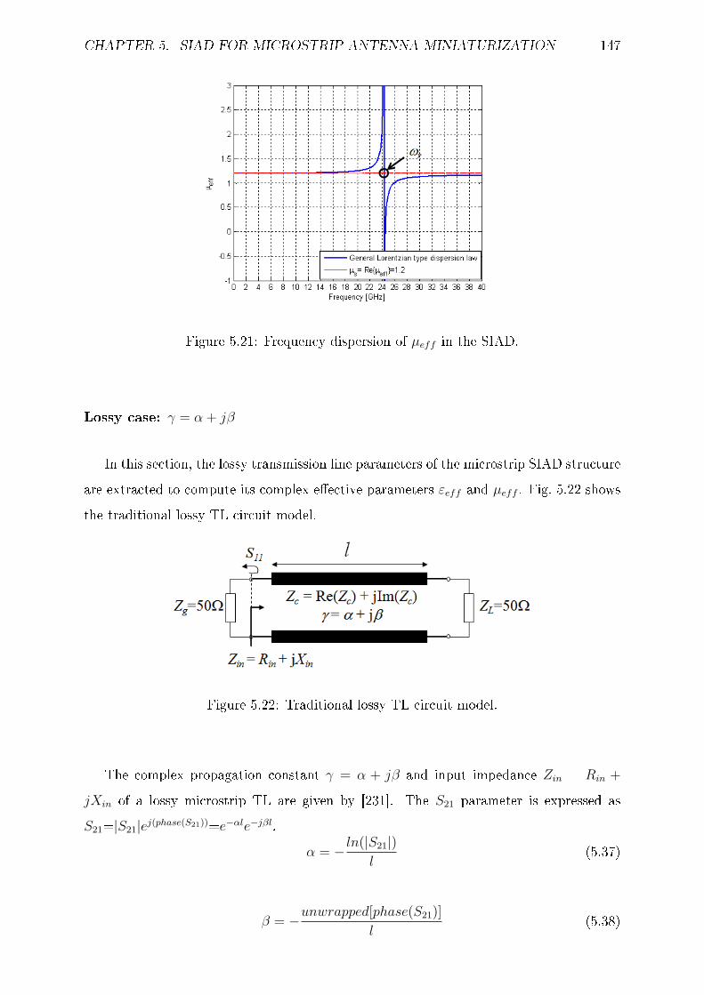
CHAPTER 5. SIAD FOR MICROSTRIP ANTENNA MINIATURIZATION 147
Figure 5.21: Frequency dispersion of µeff in the SIAD.
Lossy case: γ = α + jβ
In this section, the lossy transmission line parameters of the microstrip SIAD structureare extracted to compute its complex eective parameters εeff and µeff . Fig. 5.22 showsthe traditional lossy TL circuit model.
Figure 5.22: Traditional lossy TL circuit model.
The complex propagation constant γ = α + jβ and input impedance Zin = Rin +
jXin of a lossy microstrip TL are given by [231]. The S21 parameter is expressed asS21=|S21|ej(phase(S21))=e−αle−jβl.
α = − ln(|S21|)l
(5.37)
β = −unwrapped[phase(S21)]
l(5.38)
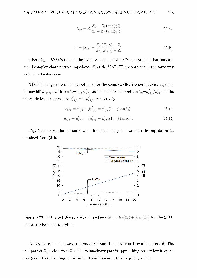
CHAPTER 5. SIAD FOR MICROSTRIP ANTENNA MINIATURIZATION 148
Zin = ZcZL + Zc tanh(γl)
Zc + ZL tanh(γl)(5.39)
Γ = |S11| = Zin(Zc, γ)− Zg
Zin(Zc, γ) + Zg
(5.40)
where ZL = 50 Ω is the load impedance. The complex eective propagation constantγ and complex characteristic impedance Zc of the SIAD TL are obtained in the same wayas for the lossless case.
The following expressions are obtained for the complex eective permittivity εeff andpermeability µeff with tan δe=ε
′′eff/ε
′eff as the electric loss and tan δm=µ
′′eff/µ
′eff as the
magnetic loss associated to ε′′eff and µ
′′eff , respectively.
εeff = ε′eff − jε
′′eff = ε
′eff (1− j tan δe), (5.41)
µeff = µ′eff − jµ
′′eff = µ
′eff (1− j tan δm), (5.42)
Fig. 5.23 shows the measured and simulated complex characteristic impedance Zc
obtained from (5.40).
Figure 5.23: Extracted characteristic impedance Zc = Re(Zc) + jIm(Zc) for the SIADmicrostrip lossy TL prototype.
A close agreement between the measured and simulated results can be observed. Thereal part of Zc is close to 50Ω while its imaginary part is approaching zero at low frequen-cies (0-2 GHz), resulting in maximum transmission in this frequency range.

CHAPTER 5. SIAD FOR MICROSTRIP ANTENNA MINIATURIZATION 149
Fig. 5.24(a) and Fig. 5.24(b) show the complex εeff and µeff .
(a) Extracted ε′eff and ε
′′eff . (b) Extracted µ
′eff and µ
′′eff .
Figure 5.24: SIAD microstrip lossy TL prototype.
Again, the measured and simulated εeff and µeff are in close agreement. The ε′′eff
and µ′′eff values associated with the electric and magnetic losses, respectively, are close
to zero in a large frequency range. At 1.9 GHz, the design frequency of the antennashown in Section 5.5, the extracted electric loss (measured tan δe = 0.0064 and simulatedtan δe = 0.0036) are higher than the dissipative losses (tan δe = 0.0012) of the commercialhost substrate. The measured magnetic losses are tan δm = 0.010, slightly higher thanthe simulated value (tan δm = 0.0040). Therefore, the SIAD losses are higher than thecommercial host RT/Duroid 6002 substrate used in the prototype. This discrepancy canbe attributed to the dispersive behavior of the host substrate, considering that additionalsources of losses are the dielectric of the host substrate and the via holes themselves.However, at low frequencies (0-2 GHz), the SIAD's losses are comparable to those of thecommercial substrates.
5.4.6 Parametric Characterization
We now characterize the SIAD microstrip structure in terms of its eective permittivityεeff and permeability µeff parameters versus frequency as a function of the via holesdiameter d, the isolation layer thickness h1 and of the structured substrate height h2,which are the most signicant parameters. The parametric analysis is done by simulationwith the commercial software CST Studio Suite 2006. Several signicant characteristicsof the proposed SIAD are observed. The corresponding full-wave simulation results arepresented in Fig. 5.25, Fig. 5.26 and Fig. 5.27, may be used as design guidelines.
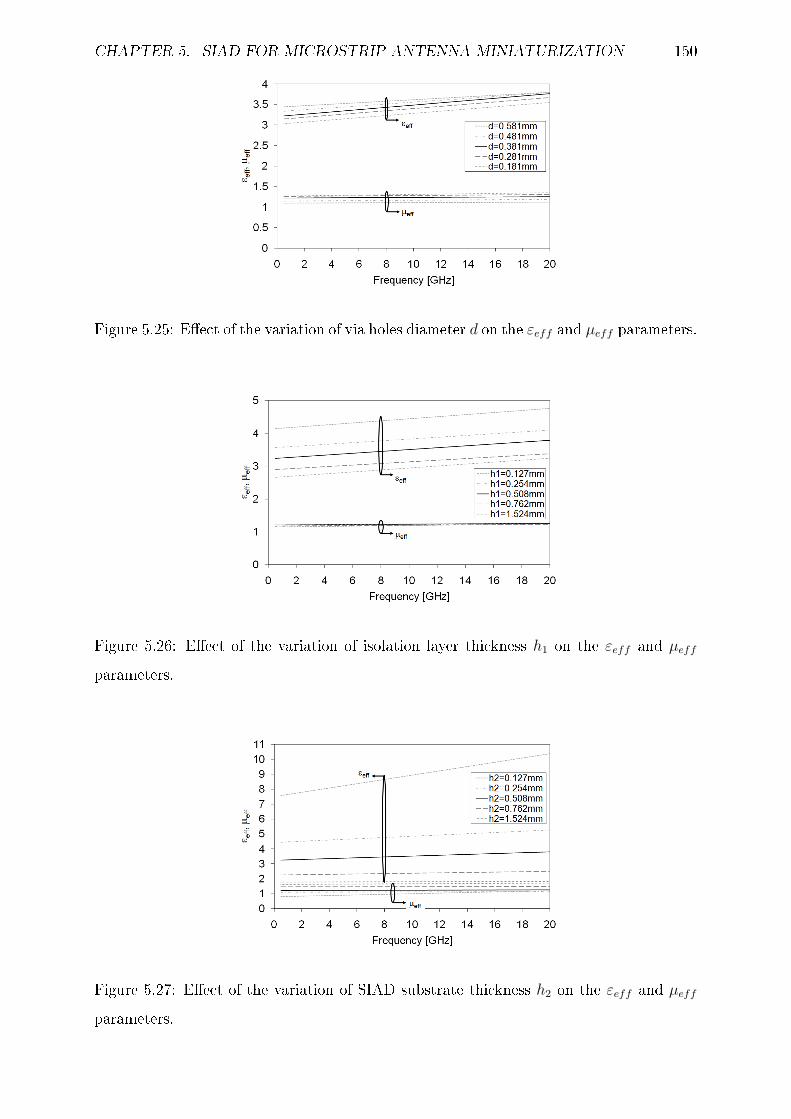
CHAPTER 5. SIAD FOR MICROSTRIP ANTENNA MINIATURIZATION 150
Figure 5.25: Eect of the variation of via holes diameter d on the εeff and µeff parameters.
Figure 5.26: Eect of the variation of isolation layer thickness h1 on the εeff and µeff
parameters.
Figure 5.27: Eect of the variation of SIAD substrate thickness h2 on the εeff and µeff
parameters.

CHAPTER 5. SIAD FOR MICROSTRIP ANTENNA MINIATURIZATION 151
From the parametric full-wave analysis, the appropriate selection of the SIAD's geo-metrical parameters can lead to an increase in the constitutive parameters up to 100% and40% for the permittivity and permeability, respectively, corresponding to an enhancementof the eective refractive index of 29% and a guided wavelength compression factor of upto 71%. Therefore, very signicant circuit size reduction may be achieved with this SIADstructure. Furthermore, using a commercial RT/Duroid 6002 host substrate with εr =2.94 (and µr = 1), a SIAD with values of εeff ranging from 1.8 to 10 and of µeff rang-ing from 1 to 1.9 has been achieved using fabrication advanced technologies (drilling andplating) currently available at the Poly-Grames Research Center. Fig. 5.28 and Fig. 5.29show the eective constitutive parameters value range of the SIAD structure for 1.9 GHz,when the via holes diameter d, the isolation layer thickness h1 and the SIAD substratethickness h2 are varied independently.
Figure 5.28: Chart design for 1.9 GHz varying via holes diameter d (in mm) and isolationlayer thickness h1 (in mm) on the constitutive εeff and µeff parameters.
Figure 5.29: Chart design for 1.9 GHz varying SIAD substrate thickness h2 (in mm) onthe constitutive εeff and µeff parameters.

CHAPTER 5. SIAD FOR MICROSTRIP ANTENNA MINIATURIZATION 152
The variations of the via holes diameter d and the SIAD substrate thickness h2 altersignicantly the constitutive parameters of the SIAD. On the other hand, the variation ofthe isolation layer thickness h1 does not signicantly change the permeability properties.
5.5 Application: Substrate Integrated Articial Dielec-tric (SIAD) Microstrip Patch Antenna
5.5.1 Description and Prototype
As an application of the SIAD presented in the previous section, a 50Ω inset-fed SIADsquare patch antenna, shown in Fig. 5.30, is designed and compared with the correspond-ing microstrip patch antenna on a commercial homogeneous RT/Duroid 6002 substrate,both operating at f0 = 1.9 GHz. Three advantages are clearly demonstrated: simpledesign and circuit size reduction, increased bandwidth and eciency. Firstly, since theSIAD is a homogeneous structure, the patch antenna design is simple, being exactlysimilar to the conventional case, except for the substitution of the eective constitutiveparameters. Although much higher size reduction can be achieved according to the para-metric full-wave analysis from the previous section, this design suces to demonstratethe proof-of-concept of the SIAD's antenna size reduction ability.
(a) Physical conguration. (b) Prototype.
Figure 5.30: Miniaturized SIAD microstrip square patch operating at 1.9 GHz.
Secondly, as seen in (5.8), for a given miniaturization factor n = √µε the antenna
bandwidth can be enhanced by increasing the ratio µ/ε (µ>ε). Lastly, the use of a SIADfor antenna miniaturization avoids the conventional use of a very high permittivity sub-

CHAPTER 5. SIAD FOR MICROSTRIP ANTENNA MINIATURIZATION 153
strate (εr1), which inherently reduces the antenna's eciency and bandwidth. Therefore,the proposed SIAD has an interesting potential for reduced-size wideband and ecientantennas.
5.5.2 Antenna Performances
The simulated and measured return losses at f0 = 1.9 GHz are presented in Fig. 5.31for the SIAD (εeff = 3.3, µeff = 1.2 and neff = 1.99) antenna compared with thehomogeneous host substrate (εeff = 2.37, µeff = 1 and neff = 1.54) and a conventionalpurely dielectric substrate (PDS) (εeff = 3.96, µeff = 1 and neff = 1.99), all having thesame substrate thickness (h = 1.016 mm). Now, in terms of bandwidth enhancement,only structures that exhibits the same size reduction (neff = √
µeffεeff = 1.99) shouldbe compared, i.e. the patch antenna printed on the SIAD substrate compared to theconventional PDS should display a bandwidth enhancement factor proportional to µeff .
The bandwidth in Fig. 5.31 are measured and simulated at -10dB. The patch antenna'sbandwidth on the homogeneous host substrate is 0.74%. Comparatively, the simulatedand measured bandwidth of the SIAD patch antenna are 1% and 2.1%, respectively.Compared with the bandwidth for the conventional PDS same-size patch of 0.52%, theSIAD's bandwidth enhancement clearly validates the theoretical prediction of (5.8). Thedierence between measurement and simulation are attributed to the dissipative losses,not included in the simulation. In this design at f0 = 1.9 GHz, where µeff is 1.2 inthe SIAD, a 92% improvement in the antenna bandwidth is observed compared to theconventional PDS. The commercial software AnsoftDesigner based on a 2.5D method ofmoment (MoM) is used to simulate the real SIAD (with vias) microstrip patch antennaprototype. In Table 5.5, the main parameters of the patch antenna printed on the SIAD,on the homogeneous host substrate and on the conventional PDS are compared. Thenumbers in brackets for BW and ηr represent the values computed by the approximateequations (5.8) and (5.19), respectively.
In terms of size, an area reduction of 24.5% of the patch antenna on the SIAD prototypeis achieved with this design (non-optimal in terms of size reduction). The parametricanalysis in Subsection 5.4.6 shows that very signicant size reduction may be achieved.
We have derived in Section 5.2 [Equations (5.8) and (5.19)] and veried by full-wave

CHAPTER 5. SIAD FOR MICROSTRIP ANTENNA MINIATURIZATION 154
analysis in Section 5.3 that for a given size (related to neff = √µeffεeff ) and for a given
amount of substrate losses (tan δe and tan δm), both BW and ηr are increase monotonicallywith increasing impedance (related to ηeff =
√µeff/εeff ). This trend is veried for BW
comparing columns a-b with column c in Table 5.5 (BWSIAD > BWPDS), where the muchlarger measured BW is most likely due to the larger substrate losses in the fabricatedprototype (imperfect vias and assembly with the isolation layer). In contrast, this trendis not veried for ηr comparing again columns a-b with column c in Table 5.5 (ηr SIAD <ηr PDS!). However, this apparent contradiction is not related to a fundamental limitation,as proven in Section 5.3, but is due to the fact that the prototype, as pointed out above, isimperfect in fabrication and has therefore higher substrate losses and dielectric than thePDS; taking into account actual increases dielectric losses in (5.19) would naturally reducethis value to a quantity closer to the measurement. Improvement of this prototype orutilization of a possible higher quality MDS could theoretically lead to eciency eectivelyhigher than that of the PDS case. The directivities obtained in Table 5.5 for the practicalSIAD follow the expected trend, but are relatively close to each other.
Figure 5.31: Measured and simulated return loss of the microstrip patch antenna on SIADsubstrate (εeff = 3.3, µeff = 1.2) in comparison with the homogeneous host substrate(εeff = 2.35, µeff = 1) and a conventional purely dielectric substrate (εeff = 3.96, µeff
= 1) operating at 1.9 GHz.

CHAPTER 5. SIAD FOR MICROSTRIP ANTENNA MINIATURIZATION 155
Measurement Simulationf0 = 1.9 GHz a b c d
SIAD Real SIAD Purely dielectric Homogeneous(with vias) substrate (PDS) host substrate
(εeff = 3.3, (εeff = 3.3, (εeff = 3.96, (εeff = 2.37,
µeff = 1.2) µeff = 1.2) µeff = 1) µeff = 1)
(including copper
conductive loss)
Refractive neff = √µeffεeff = 1.99 neff = 1.54
index neff
Wave ηeff =√
µeff/εeff = 0.60 ηeff = 0.50 ηeff = 0.65impedance
ηeff
Antenna (41.5)2 = 1722.2 mm2 (46.3)2 = 21area 43.7 mm2
-10dB BW 2.1% 1% (0.69) 0.52% (0.58) 0.74% (0.94)ηr 78% 81% (67) 84% (70) 90% (91)D 5.7 dB 5.8 dB 5.9 dB 6.5 dB
Table 5.5: Comparison between the microstrip patch antenna on the SIAD (measuredand full-wave simulated), on a PDS of the same eective refractive index and the purelydielectric host substrate of the SIAD. The numbers in brackets for BW and ηr representthe values computed by the approximate equations (5.8) and (5.19), respectively.
Finally, the simulated and measured radiation patterns of the SIAD antenna com-pared with those on the homogeneous substrate and the conventional PDS are shown inFig. 5.32(a) and Fig. 5.32(b).

CHAPTER 5. SIAD FOR MICROSTRIP ANTENNA MINIATURIZATION 156
(a) E-plane (yz-plane). (b) H-plane (xz-plane).
Figure 5.32: Radiation pattern for patch antenna operating at f0 = 1.9 GHz correspondingto various substrates of Table 5.5.
It can be observed that, despite the size reduction exhibited by the SIAD microstrippatch antenna, its radiation patterns (a and b in Fig. 5.32(a) and Fig. 5.32(b)) faithfullyresemble the ones obtained for a typical microstrip patch antenna on a conventionalsubstrate (d in Fig. 5.32(a) and Fig. 5.32(b)) with excellent cp/xp polarization isolation(∼30 dB). The dierences between simulations and measurements are attributed to edgediractions in the prototype as well as the innite ground plane in simulations.
Fig. 5.33 shows the anechoic chamber available at Poly-Grames Research Center fromÉcole Polytechnique de Montréal, where the radiation patterns of the SIAD patch antennahave been measured.
Figure 5.33: Anechoic chamber at Poly-Grames Research Center from École Polytechniquede Montréal.

CHAPTER 5. SIAD FOR MICROSTRIP ANTENNA MINIATURIZATION 157
5.6 Conclusion
A novel magneto-dielectric substrate integrated articial dielectric (SIAD) is pro-posed for miniaturized planar microstrip circuits and patch antennas. A miniaturizedand enhanced-bandwidth microstrip patch antenna using this novel SIAD has been alsopresented. Before evaluating the performance of the SIAD patch antenna, the fundamen-tal properties of a patch antenna on a magneto-dielectric substrate in terms of bandwidth,radiation eciency and directivity were revisited. The performance of a patch antennaon three ideal homogeneous substrates, a purely dielectric (PDS), a magneto-dielectric(MDS) and a purely magnetic substrate (PMS) was examined to validate the patch an-tenna's fundamental properties.
The novel SIAD, presented as a practical and planar realization of an articial magneto-dielectric substrate capable of simultaneously enhancing the eective permittivity εeff andpermeability µeff , and consequently enhanced refractive index over a broad frequencyrange, has been demonstrated numerically and experimentally. By proper design guide-lines presented in this work, an increase of up to 100% and 40% in the permittivity andpermeability respectively has been shown to be attainable leading to a guided wavelengthcompression factor of up to 71%.
Finally, a SIAD patch antenna with an area reduction of 24.5% (non-optimal in termsof size reduction) has been demonstrated and discussed in terms of bandwidth, radia-tion eciency and directivity. When compared to a purely dielectric substrate with thesame miniaturization factor as the SIAD, the SIAD patch antenna exhibited an enhancedbandwidth and eciency.
This novel articial dielectric is a potential candidate for further applications. Anintegrated quasi-optical system having planar zones of dierent refractive index in thesame substrate can be envisioned. As well, a new metamaterial substrate with left-handed behavior as a meta-substrate can be developed in the future without the use ofpatterned lines on homogeneous substrate as a conventional left-handed metamaterial. Itis anticipated that the SIAD will nd many practical applications related in miniaturized,quasi-optical and phase-engineered systems.


Chapter 6
Blockage Reduction of Support Strutsfor Antennas by Hard Surfaces toAchieve Invisibility
In the antenna area, the reduction of electromagnetic blockage is a problem that hasdeserved much attention since many years. This has been treated for problems such asthe blockage caused by the struts supporting the feed in antennas. If the mechanicalstructure (i.e. struts or masts) is part of or close to an antenna, the obstruction mayrepresent aperture blockage causing deciency in their performances.
One of the possibilities to reduce the inuence of the struts is the use of hard sur-faces. As we mention in the introduction, the struts are necessary for planar antennas asreectarrays or transmitarrays (and also for reector antennas). That is the reason whywe decided to include this study in the thesis.
In this chapter, an analysis of blocking objects caused by innitely long cylindersby using oblong cross sectional shapes and hard surfaces, with emphasis on ideally hardcylinders is done and compared to evaluate its performance. These structures have widthcomparable or sensibly larger to the wavelength. The drawbacks and advantages arehighlighted. Also, possible solutions using hard surfaces on the strut design, to reducethese obstructions and blockage eects for such cases where the direction of the incidentwave is known, are investigated and proposed. Both factors, shape and realization ofthe hard surface for the struts are fundamental to reduce blockage. In order to contrast
159
CHAPTER 6. HARD SURFACES FOR INVISIBILITY 160
the results, also some measurements will be done in future works to compare with thenumerical results.
6.1 Introduction and Motivation
Achieving "invisibility" has been the subject of extensive studies in the physics andengineering communities for decades. The use of absorbing screens [234] and antireec-tion coatings [235] to diminish the backscattering from objects are common in severalapplications, for example, you can make an object invisible to a radar with good ab-sorbers, or with a strong scattering in others directions (monostatic approach), but thisis not proper invisibility. Invisibility means to reduce the eld blockage caused by anobject, i.e. the incident wave is unperturbed in amplitude and phase after the object(to reduce the total scattered eld, in particular mainly the forward scattering). Theelectromagnetic (EM) waves should be able to pass around or through the object withoutbeing perturbed, without reections and absorptions but with a strong transmission andthe wave phase front should be keep uniform after the object. Based on this concept, inantenna applications, the electromagnetic waves radiating from or being received by anantenna are obstructed by some mechanical structures causing increased sidelobes andreduced gain of the antenna [25]. The reduction of electromagnetic blockage is a problemthat has received much attention since many years ago. In the antennas community, thishas been treated for problems such as the blockage caused by struts or masts supportingthe feed in printed reectarrays, subreectors or reector antennas. Usually in antennas,the direction of the incident wave is known, so the struts can be designed to reduce theblockage for a given direction of incidence. A good example of how to reduce the blockagecaused by these struts was presented already in 1996 [94]. Typically, in such applica-tions, the cross-section of the struts is electrically small (the width is smaller than theguided wavelength). The eld blockage from struts can be reduced for any polarization bymaking use of an oblong cross section and electromagnetically hard surfaces. This agreeswith how a hard surfaces [93] behaves, as such surfaces enhance wave propagation alongand around them (known as GO characteristics according to [236]). The hard surfaceis ideally a perfect electric conductor (PEC) with an appropriate shape for TE-case (E-eld orthogonal to the cylinder axis) and a perfect magnetic conductor (PMC) (or a highsurface impedance) for TM-case (H-eld orthogonal to the cylinder axis). There have

CHAPTER 6. HARD SURFACES FOR INVISIBILITY 161
been previous articles on methods to reduce the eld blockage due to struts in antennas.We will see in Section 6.2 that the scattered eld radiates on a cone around the strut,commonly referred to as the radiation cone of the strut. Some articles describe ways tosmear out the radiation cone, i.e. defocusing it using bent struts [237], and spreading it toseveral cones using periodic loading of the strut [238]. Previous methods only redistributethe scattered elds more uniformly in space. The gain reduction as well as the near-insidelobes are not improved. If, instead of using the approach in Kildal's paper is used,the forward scattering is reduced which, in turn, improves both the gain and the near-insidelobes; even the far-out sidelobes are reduced in average. Others papers describe alsoimprovements of the strut shape such as using triangular cross sections [239,240] or roofshapes with saw-tooth variation along the strut [241]. However, these approaches workonly when the polarization is transverse electric (TE) with respect to the axis of the strut,whereas the method described in [94] works for both TE and TM polarizations. The lat-ter is valid for rather thin objects, although extensions for thicker objects are possible byletting the waves pass along the object in a controller manner.
Reduction of EM eld blockage can also be referred to as making objects invisible toradiofrequency (RF), or simply cloaking. But cloaking and invisibility are not necessarilythe same. Properly, cloaking means to allow some volume inside to hide anything. Anobject can become invisible which does not allow arbitrary shape inside. As an example,a strut can be invisible as a thin metal for TE vertical polarization but nothing can becloaked inside. Also, cloaking of an object from electromagnetic elds means decreasingthe object's total scattering cross section whilst at the same time reducing its shadow(see Section 6.2)(in contrast to stealth technologies that reduce the backscattering crosssection).
Recently, the subject of electromagnetic cloaking, i.e. reduction of the total scatteringcross section of an object, has aroused a lot of interest in the engineering community dueto the articial structured metamaterials that have enabled unprecedented exibility inmanipulating electromagnetic waves and producing new functionalities. Radially graded-permeability and permittivity metamaterial coating capable of cloaking object from thesurrounding electromagnetic elds have been suggested [108110, 112] and also the rstrealization of an EM cloak operating in the microwave regime has been manufactured andmeasured [114]. The operation of all these previous cloak designs is based on mappingof the electromagnetic elds in such a way that the waves that come in contact with
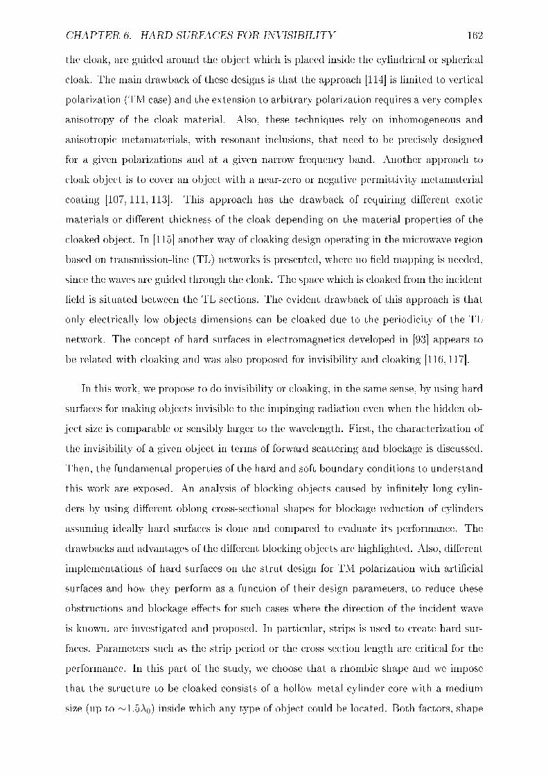
CHAPTER 6. HARD SURFACES FOR INVISIBILITY 162
the cloak, are guided around the object which is placed inside the cylindrical or sphericalcloak. The main drawback of these designs is that the approach [114] is limited to verticalpolarization (TM case) and the extension to arbitrary polarization requires a very complexanisotropy of the cloak material. Also, these techniques rely on inhomogeneous andanisotropic metamaterials, with resonant inclusions, that need to be precisely designedfor a given polarizations and at a given narrow frequency band. Another approach tocloak object is to cover an object with a near-zero or negative permittivity metamaterialcoating [107, 111, 113]. This approach has the drawback of requiring dierent exoticmaterials or dierent thickness of the cloak depending on the material properties of thecloaked object. In [115] another way of cloaking design operating in the microwave regionbased on transmission-line (TL) networks is presented, where no eld mapping is needed,since the waves are guided through the cloak. The space which is cloaked from the incidenteld is situated between the TL sections. The evident drawback of this approach is thatonly electrically low objects dimensions can be cloaked due to the periodicity of the TLnetwork. The concept of hard surfaces in electromagnetics developed in [93] appears tobe related with cloaking and was also proposed for invisibility and cloaking [116,117].
In this work, we propose to do invisibility or cloaking, in the same sense, by using hardsurfaces for making objects invisible to the impinging radiation even when the hidden ob-ject size is comparable or sensibly larger to the wavelength. First, the characterization ofthe invisibility of a given object in terms of forward scattering and blockage is discussed.Then, the fundamental properties of the hard and soft boundary conditions to understandthis work are exposed. An analysis of blocking objects caused by innitely long cylin-ders by using dierent oblong cross-sectional shapes for blockage reduction of cylindersassuming ideally hard surfaces is done and compared to evaluate its performance. Thedrawbacks and advantages of the dierent blocking objects are highlighted. Also, dierentimplementations of hard surfaces on the strut design for TM polarization with articialsurfaces and how they perform as a function of their design parameters, to reduce theseobstructions and blockage eects for such cases where the direction of the incident waveis known, are investigated and proposed. In particular, strips is used to create hard sur-faces. Parameters such as the strip period or the cross section length are critical for theperformance. In this part of the study, we choose that a rhombic shape and we imposethat the structure to be cloaked consists of a hollow metal cylinder core with a mediumsize (up to ∼1.5λ0) inside which any type of object could be located. Both factors, shape

CHAPTER 6. HARD SURFACES FOR INVISIBILITY 163
and realization of the hard surface for the struts are fundamental to reduce blockage.In order to contrast the results, also some measurements will be done in the future tocompare with the numerical results. The analysis of this work is limited to a plane wavenormally incident on an innitely long strut for a given direction of propagation for theplane wave and we propose solutions which reduce blockage simultaneously for TE andTM cases with very low blockage within a narrow frequency band.
6.2 Characterization of Invisibility
6.2.1 Introduction
The area of electromagnetic radiation is often divided into antennas and scattering.The distinction between the antenna and scattering areas lies in antennas that radiateenergy whereas in scattering a known incident wave is redirected (scattered). However,the distinction between the antenna and scattering problem is not clear. Antenna analysisinvolves also scattering analysis. Simply spoken, the area of scattering is electromagneticradiation (or reradiation) excluding antennas. This means prediction and reduction ofradar cross sections of objects, and determining the type and characteristics of a passiveobject from measurement of electromagnetic elds. Scattering from three-dimensional(3D) objects is often represented in terms of their radar cross section (RCS). This isdened as the area intercepting the amount of power that, when scattered isotropically,produces a density that is equal to the density scattered by the actual target. Consideringplane wave scattering, the RCS is dened by σ3D :
σ3D = limr→∞
[4πr2 |
−→E s|2|−→E i|2
], (6.1)
where r is the distance from the object to observation point, −→E s and−→E i are the scattered
and incident electric elds, respectively.
The corresponding parameter for a cylindrical two-dimensional (2D) object is the scat-tering width (SW) (also referred as radar cross section per unit length) dened similarlyin the fareld by :
σ2D = limr→∞
[2πr
|−→E s|2|−→E i|2
], (6.2)

CHAPTER 6. HARD SURFACES FOR INVISIBILITY 164
The study in this work is limited to a plane wave incident on an innitely long scattererwhich is a 2D scattering problem as shown in Fig. 6.1 :
Figure 6.1: Plane wave scattering (2D case).
The scattering comes from the denition of a eld problem where an object located infree space is illuminated by an incident eld, where the incident eld −→E i is the observedeld when the object is removed. The total eld −→E tot is the observed eld when the object(i.e., the scatterer) is present from which it is dened the scattered eld due to the objectas −→E s. The total eld −→E tot is dened as
−→E tot =
−→E i +
−→E s , (6.3)
The scattered eld is radiating in all directions away from the scatterer. The scatteringin the direction of propagation of the incident wave is referred to as forward scatteringand in the direction of the distant source of the incident eld is referred to as backwardscattering as shown in Fig. 6.1.
Extending to a plane wave of arbitrary incidence angle relative to the cylinder objectaxis (z-axis). The scattering occurs on a cone around the cylinder as illustrated in Fig. 6.2.

CHAPTER 6. HARD SURFACES FOR INVISIBILITY 165
Figure 6.2: Cylinder object under oblique incidence in the elevation plane.
For a given angle of incidence θ, it is known that the scattered eld radiates on a conearound the strut with cone angle equal to the π−θ. This cone is most commonly referredto as the radiation cone of the strut [239]. The scattering variation in angle of incidence isobtained by rotating the cross section of the object with respect to its normal orientation.
It is known that the total power scattered by a lossless 3D object is proportionalto the forward scattered eld. This property is most often referred to as the forwardscattering theorem or the optical theorem (see [242]). Also a corresponding theorem forcylindrical 2D objects is derived in [94]. A result of this theorem is that the scatteredelds, when average over all directions, decrease when the blockage width decreases.Forward scattering can be characterized in terms of an induced eld ratio (IFR) [243]or an equivalent blockage width (Weq) (see Subsection 6.2.3).
6.2.2 Two Dimensional (2D) Fields Color Plot
An important issue is how to characterize the invisibility or the no-blockage conditionof a given object. One possibility is to use 2D plots of the total electric eld as shownin Fig. 6.3. This representation is qualitatively useful to see whether or not an object

CHAPTER 6. HARD SURFACES FOR INVISIBILITY 166
produces a shadow or not. However, it is sometimes not evident how to compare anddetermine which of the two solutions oer low blockage. The main drawback of this rep-resentation is that a 2D eld color plots is needed for each frequency. This representationdoes not allow to characterize the invisibility in terms of frequency range in a ecientmanner.
(a) TM polarization. (b) TE polarization.
Figure 6.3: 2D E-eld color plots of the blockage for a cylinder object at 8.5 GHz.
6.2.3 Equivalent Blockage Width Weq
In order to quantify the invisibility of an object, we can use the induced eld ratio(IFR) [243] as it is known that it characterizes the forward scattered eld and to reducethis scattered eld means to achieve invisibility. This is dened in [244] as the forwardscattered eld of a cylinder illuminated by a plane wave normalized to the negative of thehypothetical scattered eld by a geometrical optics shadow of the same width, length andlocation in the plane wave as the actual object. It is even better to characterize blockagein terms of an equivalent blockage width Weq introduced in [94], that is proportional tothe product of the IFR and the physical width W . Using this, it is easy to compareobjects with respect to their invisibility. The equivalent blockage width is the width ofthe equivalent hypothetical shadow that gives the same forward scattered eld. Conse-quently, with this parameter we can quantify the blockage of an object as a function of thefrequency, for dierent polarizations and to compare dierent solutions with each otherin a rigorous way.
When an innite cylinder is immersed in an incident normal plane wave, its IFR isdened as the ratio of the forward-scattered eld (see Fig. 6.1) to the hypothetical eldradiated in the forward direction by the plane wave in the reference aperture of widthequal to the shadow of the geometrical cross section of the cylinder (object) on the incident

CHAPTER 6. HARD SURFACES FOR INVISIBILITY 167
wavefront as shown in (6.4):
IFR = −−→E s(ϕ = 0)−→E ref (ϕ = 0)
, (6.4)
where −→E s(ϕ = 0) is the forward scattered electric eld of the object and −→E ref (ϕ = 0) isthe forward scattered electric eld of a reference object.
The equivalent blockage width Weq is by denition a complex value, where both thereal part and the absolute value are representative for characterizing invisibility. Dierentinformation can be obtained from the separate analysis of its real part and absolute value.This parameter is a good measure of the blockage or shadow of a given object when it isilluminated by a plane wave. When the equivalent blockage width of the object is smallerthan the physical width W , the blockage can be considered small.
Weq = −IFR ·W , (6.5)
where IFR is the induced eld ratio and W is the physical width of the object.
Fig. 6.4 represents the plot of the equivalent blockage width of the cylinder object (seeFig. 6.3) in terms of real part and absolute value under normal plane wave incidence andfor the TE and TM polarizations. It can be seen that the equivalent blockage width (Weq)tends to be equal to the physical width (W ) at high frequency.
(a) Real part of Weq (ReWeq). (b) Absolute value of Weq (|Weq|).
Figure 6.4: Equivalent blockage width Weq for a cylinder object of physical width W =54.2 mm.
The real part of the Weq is proportional to the scattered eld averaged over all direc-tions around the cylinder. So, by reducing ReWeq, the SW is in average reduced in all

CHAPTER 6. HARD SURFACES FOR INVISIBILITY 168
directions by (6.6) from [94] for a lossless scatterer.
1
2π
∫ 2π
0
σ2D(ϕ)dϕ = 2ReWeq , (6.6)
In antenna applications, the blockage loss (BL) due to support struts in a reector isproportional to the real part of Weq (6.7), i.e. the reduction in dB of the directivity ofthe antennas due to the blockage [94].
BLdB = −10 log(|1− CsWeq|2) ,
' 8.7CsReWeq . (6.7)
where Cs depends on the diameter of the reector aperture.
The high sidelobe level (SLL) due to the struts appearing near the main lobe is pro-portional to the absolute value of Weq as explained in [25].
SLLdB = −20 log(Cs|Weq|) , (6.8)
From (6.7) and (6.8), it is evident that it is important to have the real part and absolutevalue of the equivalent blockage width as low as possible. A strut with small blockagewill have ReWeq < W and |Weq| < W .
6.2.4 Equivalent Blockage Width Calculation
The calculation of the equivalent blockage width needs the absolute scattered eldto be known. However, depending on the numerical method, the scattered eld can notalways be obtained directly from the simulations. In this work, we have employed CSTMicrowave Studio Suite 2006B as analysis tool. With this solver, the blockage width canbe computed in two dierent ways. For simplication, both use a plane wave incidentillumination and periodic boundary conditions to make the object innitely long in itsaxial direction (z-axis in Fig. 6.1) which reduce the problem to a 2D scattering problem.Note that here the angle of incidence of the wave is xed and normally to the object axis.The incidence is from left to right for the cross section shown in Fig. 6.5 and Fig. 6.6.The cross sections have a width normal to the direction of wave propagation and a lengthalong it.

CHAPTER 6. HARD SURFACES FOR INVISIBILITY 169
One possibility is to use a conventional eld probe which must be placed in the far eldinside the computation volume. With this method, two simulations must be performedto compute the scattered eld, one without object to compute the non-blocked referenceeld and another one with the object present. Then, the substraction of the two casesgives the scattered eld to be introduced in (6.9). Fig. 6.5 shows the simulation setup ofthe rst method for the equivalent blockage width characterization :
Figure 6.5: First method: simulation setup with CST Microwave Studio for TM polariza-tion.
Considering the plane wave approximation (see Annexe A.4), the equivalent blockagewidth is dened as:
Weq =
(1−
−→T 2−→T 1
)e−jπ/4
√λ0r , (6.9)
where −→T 2 = |T2|ejφ2 is the total electric eld with the object at the probe in the fareld,−→T 1 = |T1|ejφ1 is the total scattered electric eld without the object at the probe in thefareld, λ0 is the wavelength in free space and r is the distance from the object to theE-eld probe.
The other option is to directly use an E-eld fareld probe which is not located insidethe computation volume but at a fareld condition distance. With this method, CSTcode is made in such way that the eld at the fareld probe is the scattered eld (−→E s) not

CHAPTER 6. HARD SURFACES FOR INVISIBILITY 170
including the exciting incident plane wave, and the blockage width can be computed bymodifying the original equation (6.5) by (6.10) using the eld scattered by a large metalreference case (−→E ref ). Fig. 6.6 shows the simulation setup of the second method for theequivalent blockage width characterization :
Figure 6.6: Second method: simulation setup with CST Microwave Studio for TM polar-ization.
The equivalent blockage width will then be computed according to (6.10):
Weq =
−→E s−→
E ref
Wref , (6.10)
where −→E s = |Es|ejφs is the scattered eld of the object with physical width of W todetermine Weq at the E-eld fareld probe and −→E ref = |Eref |ejφref is the scattered eldof a metal reference object with physical width of Wref at the E-eld fareld probe. Thevalidation of this CST method is done in Annexe A.4.2. From [94], measurements andown computer code results are compared with the CST model dened here to validate it.
6.3 Fundamental Properties of the Soft and Hard Bound-ary Conditions
Soft and hard boundary conditions are commonly used in electromagnetics for inter-preting eld behavior on the contrary of the standard boundary condition (apply to theelectromagnetic elds on material interfaces derived from Maxwell's equations) that arealways used in all accurate eld analysis. The terminology itself comes from acoustics.

CHAPTER 6. HARD SURFACES FOR INVISIBILITY 171
The reason for these names is that these acoustics materials feel respectively soft or hardwhen touching them. Both cause total reections of an acoustic wave. Fig. 6.7 shows anillustration of a soft boundary condition at a PEC cylinder object for two-dimensional(2D) case and TM polarization, and a hard boundary condition for 2D case and TEpolarization [26].
(a) Soft boundary condition (TM case). (b) Hard boundary condition (TE case).
Figure 6.7: Fields around a perfect electric conductor (PEC) cylinder object (2D case).
Here, a 2D PEC cylinder structure oriented along the z-axis is considered and thedirection of the incident plane wave propagation is normal to the cylinder axis (z-axis) (seeFig. 6.7). Then, if the E-eld is transverse to the direction of propagation and tangentialto the cylinder axis (z-direction), i.e. −→E = Ez z (TM polarization), the wave is stoppedfrom propagating along the surface by the soft boundary condition (boundary conditionEz = 0 at the surface of the PEC or STOP characteristic). The soft boundary conditioncreates a blockage (shadow) in the direction of propagation after the object as presentedin Fig. 6.3(a). In the same way, it is clear that if the E-eld is orthogonal (normal) tothe cylinder axis (−→E = Eyy) (TE polarization), the wave can propagate along the surfacewith a strong intensity as the boundary condition is hard (also known as GO characteristicaccording to 2.4.2) with ∂En/∂n = 0 at the surface of the PEC. The PEC object has astrongly polarization dependent boundary condition for waves propagating along it. Thus,the boundary condition of a PEC cylinder object are soft for the TM case and hard for theTE case (see section 6.4). These boundary conditions are only ideally equivalent to thestandard boundary conditions for some special cases, such as for 2D problems. The termscan also be used to dene articially soft and hard surfaces which have soft and hard

CHAPTER 6. HARD SURFACES FOR INVISIBILITY 172
boundary conditions for any polarizations. Let us now consider the same propagatingwave when a plane PEC is coated with a thin dielectric layer of dielectric constant εr
and thickness d. Inside the dielectric coating the propagation constant will be kε = √εrk
which is larger than the k outside the coating. The component of kε along the dielectricsurface must be equal to k. Therefore, we will get a normal component of the propagatingvector inside the dielectric coating equal to ky =
√k2
ε − k2 = k√
εr − 1. This componentof k will transform the boundary condition at the metal surface to the boundary conditionof an articial magnetic conductor (AMC) at the surface of the dielectric: kyd = π/2,i.e. d = λ0/4
√εr − 1. Therefore, from duality PEC-PMC, it is seen that this dielectric
coating PEC surface provides the soft boundary condition for the normal eld ((−→E =
Eyy)) and the hard boundary condition for the transverse tangential eld (−→E = Ez z)(see Section 6.5), i.e. the opposite of the boundary conditions on a PEC (hard casefor TE is a PEC and for TM is a PMC or AMC). The polarization independent hardboundary condition is obtained by loading the surface of the dielectric coating PEC surfacewith metal strips (PEC/PMC strip grid) in the direction of the electromagnetic wavepropagation (x direction) as presented in Fig. 6.8(b) (see Section 6.6). This means thatindependently of the polarization of the E-eld (TM case (vertical polarization) and TEcase (horizontal polarization)), when the metal strips are oriented longitudinally in thesame direction as the waves propagate (hard case (Fig. 6.8(b))) it will allow the wave topass along the surface (GO condition). And when the strips are oriented transverse to thedirection of propagation (soft case (Fig. 6.8(a))), this will stop waves propagation along thesurface (STOP condition). The hard surface has what is referred to as GO characteristicsin contrast to the STOP characteristics of the soft surface (see Subsection 2.4.2 and [236]).
(a) Soft surfaces for TE & TM cases. (b) Hard surfaces for TE & TM cases.
Figure 6.8: Soft and hard surfaces.
In antenna applications, the smallest blockage width is obtained for the hard sur-face, because this provides the correct boundary conditions for waves to propagate as

CHAPTER 6. HARD SURFACES FOR INVISIBILITY 173
undisturbed as possible around the struts for a given direction of incidence and for anypolarization.
6.4 Shaping the Cross Section of a TE Hard Strut
As explained in Section 6.3, as far as the hard or GO condition is obtained, the waveswould be guided around the cylinder surface. For the TE case, the ideal hard surfaceis a PEC, thus it is straightforward to implement it. Nevertheless it is also known thatthe shape of the cross section plays an important role in blockage reduction, and it hasbeen stated from antenna applications that oblong cross sectional shapes are required tominimize that blockage [25]. From [94], it is known that a metal strut has an ideallyhard surface for TE case and will be invisible when it is thin (width W of the strut ismuch smaller than the wavelength λ0). Here, we choose to study normal incidence onPEC (realized as metal) cylinders for TE-case, but the results are valid also for TM-case,PMC cylinders and for dual polarization for ideally hard dual-polarized struts. In thissection, an analysis of dierent cross sectional shapes of physical width W=54.2 mm ofideal hard struts are studied to compare performance in terms of blockage (or invisibility)over a large frequency band (0.1 - 20GHz) to nd out how thick a thin strut can be andstill be quite invisible under normal incidence and varying the angle of incidence ϕ in theazimuth plane.
6.4.1 Equivalent blockage width Weq under normal incidence (ϕ =
0)
Initially, the simulation results for ideally PEC hard cylinders object of dierent crosssectional shapes with the same physical width are computed. Some assumptions arespecied to represent the results: the objects are considered innitely long cylinders inthe cylinder axis direction. The plane wave is propagating under normal incidence (i.e.E-eld orthogonal to the cylinder axis) as shown in Fig. 6.9.

CHAPTER 6. HARD SURFACES FOR INVISIBILITY 174
Figure 6.9: Metallic rhombus of physical width W = 54.2 mm for ϕ = 0.
The real part and the absolute value of the equivalent blockage width Weq of cylin-ders with circular, rhombic, star-shaped and thin rectangular cross sections are shown inFig. 6.10. The latter is oriented orthogonal to the direction of wave propagation and hasthe same width as the other cylinders. The thickness of the rectangular cross section is 1mm, and this is the same for both the transverse and longitudinal part of the star-shapedcross section. In these simulations, we used physical cross sections of all cylinders of W= 54.2 mm, and we show the equivalent blockage widths in the frequency range 0.1 to 20GHz (0.018λ0 to 3.6λ0). However, the simulation results are presented as a function of thephysical width W/λ0. These results show that the rhombic cross section of the strut hasthe smallest real part and absolute value of Weq when the physical width W is comparableor sensibly larger than the wavelength λ0 (ReWeq, |Weq| < W up to ∼ 1.5λ0) (at 8.5GHz (λ0=35.3 mm) and W=54.2 mm ⇒ W/λ0 = 1.53), whereas the star shaped andthin rectangular cross section is best when the physical cross section is narrower than ap-proximately W/λ0=0.04. The thin rectangular cross section is explained as a quasi-staticsolution. The cross section is so narrow in terms of wavelength that transverse currentscannot be induced. The star-shaped cross section works like the transverse rectangularcross section, because the orthogonal rectangular part making up the two other arms ofthe star are invisible to the wave because of their small thickness.

CHAPTER 6. HARD SURFACES FOR INVISIBILITY 175
(a) ReWeq/W . (b) |Weq|/W .
Figure 6.10: Equivalent blockage width under normal incidence of ideally hard cylinderswith dierent basic-shaped cross-sections of physical width W = 54.2 mm.
Fig. 6.11 presents the equivalent blockage widths of cylinders with rhombic cross sec-tions. The results show that oblong rhombic cross section have smaller blockage widthwhen the physical width W is comparable or sensibly larger to the wavelength, exceptfor very narrow widths in terms of frequency where in this case the shorter rhombic isbest. This is in agreement with the results of Fig. 6.10 that the transverse strip (thinrectangular cross section) is the best for narrow cross sections.
(a) ReWeq/W . (b) |Weq|/W .
Figure 6.11: Equivalent blockage width under normal incidence of ideally hard cylinderswith rhombic cross-sections of physical width W = 54.2 mm and dierent lengths L
(L=2W and L=4W ).
The equivalent blockage width Weq of metal struts can be reduced signicantly if the

CHAPTER 6. HARD SURFACES FOR INVISIBILITY 176
shape of the strut cross section is numerically optimized. An initial study of what can beachieved has been performed in [245]. An optimization algorithm was used to numericallyoptimize the metallic cross section shape with the purpose of reducing its blockage widthfor TE polarization. The optimized shape has been restricted such that the cross sectionhas one symmetry plane and does not have sharp corners, except at its endpoints in thedirection of wave propagation. The cross section is constrained to a minimum width ofW=3 mm and a maximum length of L=7 mm over the frequency interval from 8 GHz to17 GHz. The achieved nal cross section is represented in one of the insets of Fig. 6.12(a)and has a star shape. Fig. 6.12 compare the equivalent blockage width of three crosssections that are identical in terms of physical width W=54.2 mm and length L=108.4mm. One of these has been numerically shape-optimized for lowest average blockagewidth over a given frequency, for a xed physical width W=3 mm and length L=7 mm.This frequency range (8-17 GHz) corresponds to the xed physical width being between0.08 and 0.17λ0 as shown in Fig. 6.12(a). In comparison with Fig. 6.11 we can observethat the strut with the rhombic shape yields an equivalent blockage width that is largercompared with the optimized shape when the physical width is smaller than 0.2λ0, despitethe fact that the physical width and length of the two cross sections are identical. On thecontrary, when the physical width W is comparable to the wavelength λ0, the blockage issmaller with the rhombic strut than the optimized strut.
(a) ReWeq/W . (b) |Weq|/W .
Figure 6.12: Equivalent blockage width under normal incidence of ideally hard cylinderswith dierent star-shaped cross-sections of physical width W = 54.2 mm.
The obtained results may be used as charts for the strut designs over a large frequencyband (0.1 - 20 GHz) to reduce the obstruction and blockage eects in antenna applications.
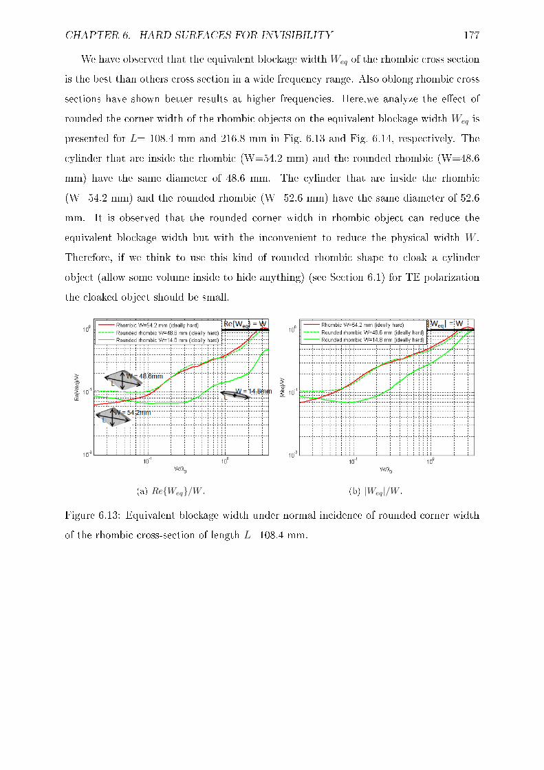
CHAPTER 6. HARD SURFACES FOR INVISIBILITY 177
We have observed that the equivalent blockage width Weq of the rhombic cross sectionis the best than others cross section in a wide frequency range. Also oblong rhombic crosssections have shown better results at higher frequencies. Here,we analyze the eect ofrounded the corner width of the rhombic objects on the equivalent blockage width Weq ispresented for L= 108.4 mm and 216.8 mm in Fig. 6.13 and Fig. 6.14, respectively. Thecylinder that are inside the rhombic (W=54.2 mm) and the rounded rhombic (W=48.6mm) have the same diameter of 48.6 mm. The cylinder that are inside the rhombic(W=54.2 mm) and the rounded rhombic (W=52.6 mm) have the same diameter of 52.6mm. It is observed that the rounded corner width in rhombic object can reduce theequivalent blockage width but with the inconvenient to reduce the physical width W .Therefore, if we think to use this kind of rounded rhombic shape to cloak a cylinderobject (allow some volume inside to hide anything) (see Section 6.1) for TE polarizationthe cloaked object should be small.
(a) ReWeq/W . (b) |Weq|/W .
Figure 6.13: Equivalent blockage width under normal incidence of rounded corner widthof the rhombic cross-section of length L=108.4 mm.

CHAPTER 6. HARD SURFACES FOR INVISIBILITY 178
(a) ReWeq/W . (b) |Weq|/W .
Figure 6.14: Equivalent blockage width under normal incidence of rounded corner widthof the rhombic cross-section of length L=216.8 mm.
6.4.2 Equivalent blockage width Weq under the variation of inci-dence angle ϕ
As mentioned before, an analysis of the rhombic cross section of physical widthW=54.2 mm in terms of lower blockage width over a large frequency band (0.1 - 20GHz)to nd out how thick a thin strut can be and still be quite invisible with varying the angleof incidence ϕ of the plane wave incidence in the azimuth plane is presented here.
The setup for analyzing the blockage width with variation of the incidence angle ϕ inthe azimuth plane is presented in Fig. 6.15.
Figure 6.15: Metallic rhombus of physical width W = 54.2 mm varying the incidenceangle ϕ in the azimuth plane.
The analysis of the eect of varying the plane wave incidence angle impinged on the

CHAPTER 6. HARD SURFACES FOR INVISIBILITY 179
rhombic objects is presented for L= 108.4 mm and 216.8 mm in terms of the equivalentblockage width Weq in Fig. 6.16 and Fig. 6.17, respectively.
(a) ReWeq/W . (b) |Weq|/W .
Figure 6.16: Equivalent blockage width under variation of incidence angle ϕ in the azimuthplane of the rhombic cross-section of length L=108.4 mm.
We can observe that the rhombic cross section depends strongly on the incidence angleϕ of the plane wave in the azimuth plane. The rhombic cross section of L=216.8 mmis more sensitive to the incidence angle than the L=108.4 mm. This means that oblongcross section are the best in terms of reduction of the blockage width for normal incidencebut worse for the variation of incidence angle ϕ. In the future, the work will be extendedto a plane wave of arbitrary incidence angle θ relative to the cylinder axis (see Fig. 6.2).
(a) ReWeq/W . (b) |Weq|/W .
Figure 6.17: Equivalent blockage width under variation of incidence angle ϕ in the azimuthplane of the rhombic cross-section of length L=216.8 mm.
CHAPTER 6. HARD SURFACES FOR INVISIBILITY 180
6.5 Hard TM Case
The hard condition for the TM polarization can also be easily achieved in the simplestway by coating the rhombic cross section with a dielectric material with relative permit-tivity εr and thickness d = λ0/4
√(εr − 1). It is important also how to nish the dielectric
at the edges. The dielectric material must not be stretched out in sharp edges like theoblong rhombic cross section, it must be truncated at the sharp edges of the structure.As it was discussed in [94], the sharp edges in the dielectric coating have a big inuencein destroying the hard condition. The cross section of such strut is described in Fig. 6.18.
Figure 6.18: Dielectric coating of a metallic rhombus.
Considering a rhombic width of W = 54 mm and length of L = 216.8 mm, a comparisonof the blockage for TM case in 2D E-eld color plot at 8.5 GHz of the rhombus without andwith dielectric coating is illustrated in Fig. 6.19 and in terms of equivalent blockage widthWeq in Fig. 6.20. In this case the physical width W is about 1.5 larger than the wavelengthλ0. A shadow (strong blockage) is observed in Fig. 6.19(a) and Fig. 6.20(a) due to the softcondition in TM case for a metallic structure and a lower blockage as expected is seen inFig. 6.19(b) and Fig. 6.20(b) at 8.5 GHz because of coating the rhombus with dielectricmaterial that provide the articially hard surface for the TM case. The dielectric coatingis a simple way to implement TM case.

CHAPTER 6. HARD SURFACES FOR INVISIBILITY 181
(a) Without covering. (b) With covering (dielectric material coating withεr = 2.2).
Figure 6.19: 2D E-eld color plots of the blockage of a rhombus (W=54.2 mm and L=216.8mm) for TM polarization at 8.5 GHz.
(a) Without covering. (b) With covering (dielectric material coating withεr = 2.2).
Figure 6.20: Equivalent blockage width Weq of a rhombus (W=54.2 mm and L=216.8mm) for TM polarization under normal incidence.
The design is done for the frequency f = 8.5 GHz (λ0 = 35.3 mm). Note that thefrequency can be tuned by changing the thickness d of the dielectric material and itsdielectric constant εr. Here we use a Taconic TLY-5 as dielectric substrate with εr = 2.2,tanδ=0.0009 and thickness d = λ0/4
√(εr − 1) = 8.05 mm at 8.5 GHz. The behavior of
the blockage for TM case as a function of both the rhombic length L and the type ofdielectric material employed for the coating εr is analyzed and is presented in Fig. 6.21.The total width Wtot depends on the material. The higher the dielectric constant εr of thematerial, the narrower the bandwidth in which the equivalent blockage width Weq is belowthe physical width W , as expected (Fig. 6.21(a)). On the other hand, the performancebecomes worse with the shorter length L, but this length can be much more reduced than

CHAPTER 6. HARD SURFACES FOR INVISIBILITY 182
for TE metallic case without aecting the blockage (Fig. 6.21(b)). The reason comes fromthe type of surface that propagate in the TM case due to the substrate, which are notpresent in the TE case. The simulations are done considering the substrate losses. Theresults of the absolute value of Weq (|Weq|) for the variation of L and εr are presented inAnnexe A.4.3.
(a) Eect of the rhombic length L for εr = 2.2. (b) Eect of the dielectric constant εr for a rhombiclength L = 216.8 mm.
Figure 6.21: TM performances for a metallic rhombus with a dielectric coating undernormal incidence.
The values of the dielectric thickness d for dierent dielectric constant εr of the sub-strate at 8.5 GHz (λ0 = 35.3 mm) are summarized in Table 6.1.
Substrate type Dielectric constant εr Dielectric thickness d
Taconic TLY-5 2.2 8.05 mmTaconic TLC-32 3.2 5.95 mmArlon AR-450 4.5 4.72 mmArlon AR-600 6 3.95 mm
Rogers TMM 10 9.2 3.08 mmRogers RT/Duroid 6010 10.8 2.82 mm
Table 6.1: Dielectric thickness d = λ0/4√
(εr − 1) of the substrate for dierent dielectricconstant εr at 8.5 GHz.
Fig. 6.22 depicted the eect of the variation of incidence angle ϕ for TM polarizationin a metallic rhombus (W=54.2 mm and L=216.8 mm) with dielectric coating εr = 2.2.

CHAPTER 6. HARD SURFACES FOR INVISIBILITY 183
Figure 6.22: TM performances for a metallic rhombus (W=54.2 mm and L=216.8 mm)with a dielectric coating εr = 2.2 under variation of incidence angle ϕ in the azimuthplane.
It is observed that oblong metallic rhombus with a dielectric coating is very sensitivefor the TM polarization when the incidence of the plane wave is varying with angle ϕ inthe azimuth plane. When ϕ > 15, the performance in terms of equivalent blockage widthWeq or invisibility is worse because Weq > W. In Annexe A.4.3, the absolute value of Weq
is illustrated.
The hard surface is ideally a perfect electric conductor (PEC) for TE-case (E-eldorthogonal to the object axis) and a perfect magnetic conductor (PMC) for TM-case (Held orthogonal to the object axis). We analyze normal incidence on ideal PMC rhombiccross section of physical width W=54.2 mm for TM-case in comparison with ideal PECrhombic cross section for TE-case in terms of equivalent blockage width for L=2W=108.4mm and L=4W=216.8 mm in Fig. 6.23 and Fig. 6.24, respectively. The ideally PMCsolid rhombic cross section is modeled in CST Microwave Studio 2006 using a magneticmaterial with εr=1 and µr > 1000, here µr=10000. The dierence between the equivalentblockage width for PEC solid material and PMC solid material are because it exists forthe moment no possibilities to dene a PMC material, so the magnetic material withµr > 1000 allow to approximate the ideal PMC material.

CHAPTER 6. HARD SURFACES FOR INVISIBILITY 184
(a) ReWeq/W . (b) |Weq|/W .
Figure 6.23: Equivalent blockage width under normal incidence of ideally PMC rhombiccross-section of physical width W=54.2 mm and length L=2W for TM case.
(a) ReWeq/W . (b) |Weq|/W .
Figure 6.24: Equivalent blockage width under normal incidence of ideally PMC rhombiccross-section of physical width W=54.2 mm and length L=4W for TM case.
We can observe that the bandwidth is improved by using magnetic material in compar-ison with the narrow bandwidth of the dielectric coating results illustrated in Fig. 6.20(b).The obtained results for a ideally PMC solid rhombic cross section for TM polarizationcorroborate the results obtained for a PEC solid rhombic cross section for TE polarizationin the two case (L=108.4 mm and 216.8 mm). It is interesting to compute ideal casesof struts because it will provide more general results than studying a specic realization,which will be useful in determining fundamental physical limitations. Also, metal strutsare ideally hard for TE case. The obtained results of ideal struts in this work allow

CHAPTER 6. HARD SURFACES FOR INVISIBILITY 185
getting design chart that gives some performance goals for a nal realized strut. Bothfactors, shape and realization of the hard surface for the struts are fundamental to achieveinvisibility.
6.6 Simultaneously Blockage Reduction for TE and TMCases
The concept for creating invisibility for both TE and TM cases by using hard surfacesand oblong cross sectional shapes (see Section 6.3), and in particular a some cross sectionshape struts are only valid for rather objects which physical widths W which are muchsmaller than the wavelength, although extension for objects which W is comparable orsensibly larger than the wavelength are possible by letting the waves pass along the objectin a controlled manner. It is the purpose here to analyze whether or not we can obtaininvisibility over a large frequency band with rhombic cross section even for struts whichW is comparable or sensibly larger than the wavelength. This study nds out how thicka strut can be and still be quite invisible in a frequency band. Here we impose as aconstraint that the structure to be cloaked (i.e. to hide objects inside it) consists of ahollow metal cylinder core of a diameter 52.6 mm (up to ∼ 1.5λ0 at 8.5 GHz) inside whichany type of object could be located. In particular, a metallic rhombus core with xedwidth W = 54.2 mm will be used as Fig. 6.25 shows. Also, we reduce the problem tonormal propagation direction and variation of incidence angle ϕ of the plane wave in theazimuth plane, but two polarizations (TE and TM). The proposed solution are describedin Fig. 6.25(a) where the cross section of the innite cylinder is shown.
When the cylinder has to present a low blockage for two polarizations, a metamaterialsurface should be employed, i.e. a surface which is hard for both polarizations at thesame time. These conditions can be obtained as a PEC conductor for TE case and adielectric coating or PMC conductor for TM case as seen in Section 6.4 and 6.5. If wewant to make a strut that has small blockage widths for both TE and TM cases, this canbe obtained experimentally by loading the dielectric coating with metal strips running inthe direction of propagation wave across the struts. The strips should preferably go outin sharp edge at the corners where the dielectric coating is truncated (see Section 6.5).The strip dimensions do not have much eect on the performance except that there must

CHAPTER 6. HARD SURFACES FOR INVISIBILITY 186
be more than two strips per wavelength. The frequency can be tuned by changing thethickness of the dielectric material. Here, an analysis including the extension to struts ofphysical width W up to 1.5λ0 is presented. The structure is described in Fig. 6.25. As itcan be observed a cylinder object can be cloaked inside the structure. Note that here thestrips, that allow the hard condition for TE polarization, must be terminated as sharpedges as the oblong metallic cross section.
(a) Strut view.
(b) Cross-section.
Figure 6.25: Cloaked cylinder in a rhombic cross section with hard surface covering real-ized with narrow metallic strips for dual polarization cloaking.
It is known that the period of the strips has to be smaller compared to the wavelengthto have the correct hard behavior. In Fig. 6.26, the eect of the period of the employedstrips in the performance of TE and TM modes is presented. Here again, the rhombuswidth W = 54.2 mm is kept constant and the blockage reduction is analyzed from 1 to20 GHz, i.e. W between 0.18λ0 and 3.6λ0. The rhombus length L=216.8 mm is chosento be four times the width W , the dielectric has permittivity εr=2.2 and its thickness isd=8.05 mm. From Fig. 6.26(a) and Fig. 6.26(b), we can conclude that TM case is not verysensitive to this parameter but TE case requires that the period p has to be small enough(the ratio between period p and the strip width s should be less than p/s=2) to keepa low blockage at high frequency. The ripples that appear are due to the surface wavespropagation. We can also observe in Fig. 6.26(b), a small shift in frequency considering

CHAPTER 6. HARD SURFACES FOR INVISIBILITY 187
that the design frequency is at 8.5 GHz.
(a) TE case. (b) TM case.
Figure 6.26: Equivalent blockage width under normal incidence : changing the strip periodp with strip width s = 3 mm.
Another important parameter that was already checked in Section 6.4 is the totallength Ltot. This solution, by using strips to create the dual hard surface, increases thetotal length of the cross section from L to Ltot for a given width, here W = 54.2 mmas shown in Fig. 6.27. When the total length is changed, the TM case is unaected asit happened for the solution with only dielectric coating (Fig. 6.21(a)), however TE caseexhibits a worse performance when the total length is reduced.
(a) TE case. (b) TM case.
Figure 6.27: Equivalent blockage width under normal incidence: changing the rhombuslength L: with strip period p = 6 mm and strip width s = 3 mm.
Fig. 6.28 show TE and TM performances of the rhombic cross section (W = 54.2

CHAPTER 6. HARD SURFACES FOR INVISIBILITY 188
mm and L = 216.8 mm) with a hard surface covering realized by dielectric coating andwith narrow metallic strips for dual polarization when the incidence angle ϕ varies in theazimuth plane.
(a) TE case. (b) TM case.
Figure 6.28: TE and TM performances under variation of incidence angle ϕ in the azimuthplane: with strip period p=6 mm and with strip width s = 3 mm.
It is observed that both TE and TM cases are very sensitive to the variation of theincidence angle ϕ and the blockage reduction is bad. The best case is for normal incidence(ϕ= 0) where the invisibility is quite good at 8.5 GHz in a narrow band for the TE andTM polarization simultaneously.
As mention in Section 6.5, the hard surface is ideally a perfect electric conductor (PEC)for TE-case (E-eld orthogonal to the object axis) and a perfect magnetic conductor(PMC) for TM-case (H eld orthogonal to the object axis). Here, it is analyzed thenormal and variation of incidence angle ϕ in the azimuth plane on ideal PMC rhombiccross section of physical width W=54.2 mm and length L=216.8 mm with narrow metallicstrips for dual polarization in terms of equivalent blockage width. As in Section 6.5, theideally PMC solid rhombic cross section is modeled in CST Microwave Studio 2006 using amagnetic material with εr=1 and µr > 1000, here µr=10000. As the rhombic cross sectionis PMC material, we can observe that for the TM case (Fig. 6.29), the equivalent blockagewidth is no more narrow band as it happened with dielectric coating (Fig. 6.26(b)), but ithas the same behavior as the TE-case. Fig. 6.29 shows that for TE and TM polarizationunder normal incidence, this strut is almost invisible in a large frequency band.

CHAPTER 6. HARD SURFACES FOR INVISIBILITY 189
Figure 6.29: Equivalent blockage width under normal incidence of a ideally PMC hardstrut with narrow metallic strips: with strip period p = 6 mm and strip width s = 3 mm.
In Fig. 6.30, the eect of the incidence angle ϕ in the azimuth plane on the ideal PMCstruts with narrow metallic strips is presented. Fig. 6.30(a) and Fig. 6.30(b) show similarbehavior and that the structure is very sensitive to the variation of incidence angle ϕ. Atϕ = 20, this structure has smaller blockage for a narrow bandwidth.
(a) TE case. (b) TM case.
Figure 6.30: Equivalent blockage width under variation of incidence angle ϕ in the azimuthplane of a ideally PMC hard strut with narrow metallic strips: with strip period p = 6mm and strip width s = 3 mm.
These struts have a surface consisting of parallel metallic strips on ideal PEC or PMCstruts, so that the strut works ideally as a hard surface for dual polarization when thedirection of the strips is parallel to the plane of incidence of the plane wave on the strut.

CHAPTER 6. HARD SURFACES FOR INVISIBILITY 190
The analysis is done in case when the plane of incidence is aligned with the strip direction.In a future work, an analysis when it deviates from it, will be realized to determine thesensitivity of the equivalent blockage width of the direction of incidence θ (under obliqueincidence in the elevation plane).
6.7 Measurement Setup in the Anechoic Chamber
The measurements will be done with the setup described in [94, 244] and shown inFig. 6.31. The incident wave is normal to the object-length axis
Figure 6.31: Measurement setup for measuring the equivalent blockage width of scatterers.
First, the transmission −→T 1 between two horn antennas (one transmits and the otherreceives) is measured without any object in between them. Thereafter, the transmission−→T 2 was measured with the object present. Note that the object should be located inthe fareld of the two horns (r′ , r > 2(W )2/λ0) and should be so long that the apertureillumination angle at -10dB of the horns should illuminate the entire object of physicalcross-section width W . Finally, the equivalent blockage width is calculated as
Weq =
(1−
−→T 2−→T 1
)e−jπ/4
√λ0|r′ |r|r′|+ |r| , (6.11)
where λ0 is the wavelength in free space, r′ is the distance from the phase center of
the transmit horn antenna to the object (where r′ is negative) and r is the distance
from the object to the receive horn antenna. The measurements are done by using a

CHAPTER 6. HARD SURFACES FOR INVISIBILITY 191
network analyzer which stored the scattering parameters value of −→T 1,−→T 2 and provided
the amplitude and phase of the ratio −→T 2/−→T 1 as output after the second measurement.
The amplitude |T2|dB−|T1|dB and phase φ2deg.−φ1deg. must be transformed to a complexratio −→T 2/
−→T 1 = 10(|T2|dB−|T1|dB)/20ej(φ2deg.−φ1deg.) before insertion in (6.11).
6.8 Conclusion
Blockage can be reduced by using hard surfaces and special cross sectional shapes.By computing the equivalent blockage width of ideally hard cylinders of dierent crosssections, we have shown that the oblong cross section is the best when the physicalwidth is larger than about 0.2λ0, whereas for narrower cross-sections the transverse thinrectangular cross-section is better. The latter can be strengthened by a star-shaped crosssection, without signicant change in the blockage width. The latter was found as aresult of numerical optimization. The optimized oblong shape is explained by a smoothtransition of the waves past the cylinder, which is facilitated by the GO characteristics ofthe hard surface. The thin rectangular cross section is explained as a quasi static solution.The cross section is so narrow in terms of wavelength that transverse currents cannot beinduced. The star-shaped cross-section works like the transverse rectangular cross-section,because the orthogonal rectangular part making up the two other arms of the star areinvisible to the wave because of their small thickness. It must be emphasized that wehave treated ideally hard cylinders. This makes the results valid for metal cylinders andTE-case. The design charts allow to characterize and compare performances of dierentcross sectional shapes of ideal struts in terms of equivalent blockage width over a largefrequency band (0-20 GHz). These comparisons nd out how thick a strut can be andstill be quite invisible.
The performance for TM-case depends on the realization of the PMC surface, but theresults can be seen as typical performance at the center frequency. The bandwidth willnormally be small, but can be up to 15% when the articial magnetic conductor is realizedby dielectric coatings as shown in [94]. With the focus on relatively electrically large crosssection, the performance of the most simple realization of a TM hard surface (dielectriclayer) has been analyzed. This geometry is less sensitive to the cross sectional lengththan the TE case, but the bandwidth is narrower and depends on the type of material

CHAPTER 6. HARD SURFACES FOR INVISIBILITY 192
used. Also, the variation of incidence angle ϕ in the azimuth plane is very sensitive forthe TM case. While the ideal PMC solid rhombic cross section allow wider bandwidthcomparable with the ideal PEC structures.
Articial surfaces can also be used as coatings to reduce the blockage caused by strutswith rhombic cross sectional and relatively large width. A type of coating solutions whichreduce blockage simultaneously for TE and TM cases is proposed. The solution is basedon hard surfaces made with narrow metallic strips and it has been proven how parameterssuch as the strip period and the rhombus length are critical for TE performance. Theperformance for TM case is also good but only within a very narrow band. The dielectriccoating is a simple way to implement TM case. The bandwidth is always limited by TMcase, since TE case has wide band in most cases. Considering ideal PMC hard rhombiccross section with narrow metallic strips, the results show wide band behavior in terms ofequivalent blockage width and it is very sensitive to the variation of incidence angle ϕ inthe azimuth plane. In order to contrast the results, in a short term some measurementswill be achieved to compare with the numerical results. Future solutions can be the use ofa mushroom-type meta surface [9,10] for dual polarization, but this solution is to narrowband. Also an analysis when the strips deviates from the plane of incidence of the planewave on the strut will be realized in a future work, to determine the sensitivity of theequivalent blockage width of the direction of incidence θ (oblique incidence in the elevationplane). It is interesting to compute ideal cases of struts because it will provide moregeneral results than studying a specic realization, which will be useful in determiningfundamental physical limitations. The obtained results of ideal struts allow getting designchart that give some performance goals for a nal realized strut. Both factors, shape andrealization of the hard surface for the struts are fundamental to achieve invisibility.

Chapter 7
General Conclusions, Future Work andPublications
The work carried out along this thesis covers several applications of metamaterialstructures in planar antennas from the design and analysis to comparison with the proto-type implementation and evaluation. Each one of the chapters has been devoted to onespecic topic, but all of them are guided by the same objectives: extending the knowl-edge of the analysis, design and operation of the metamaterial structures to contributeand propose possible solutions that help to improve the planar antenna performances us-ing these novel structures. Although specic conclusions have been presented at the endof each chapter, we summarize here the main conclusions of the overall work, and alsothe research lines that are proposed for the future.
The research work that has been done throughout this thesis has been accepted forpublication in several technical journals. Moreover, the work has been presented at themain international conferences in the eld of antennas. These contributions are mentionedhere.
7.1 General conclusions and contributions
In this thesis, we have presented a collection of numerical and experimental resultsto contribute on dierent potential applications of metamaterials for improving planarantenna performances. During the last few years, there has been a growing interest in
193

CHAPTER 7. GENERAL CONCLUSIONS, FUTURE WORK 194
developing articially engineered structured materials. Previous studies have revealedthat there are numerous metamaterial able to enhance the antenna and microwave circuitperformances. As a result, a signicant increase in the research on these materials hasbeen observed in the antenna community. Despite the great research eort that has beingcarried out, there are still quite an amount of investigation in the metamaterial area thatshould be done before these structures in antennas can be considered a mature solutionto improve their performances.
The eect of AMC structures is analyzed and presented, placed as sidewalls and aspropagation strips within an oversized waveguides at 12 GHz band to enhance wave guid-ance and improve the performance of parallel-plate slot antennas. According to the sim-ulated and measured eld distributions in the parallel-plate waveguide, the results showvery satisfactory properties using these structures to enhance and guide the wave prop-agation in this kind of distribution waveguide. These two concepts are illustrated bytwo possible antenna applications analyzed in detail and validated experimentally. Theresults of the AMC sidewalls show a quite good uniform eld distribution inside the over-sized waveguide but a slight improvement in the antenna application performances dueto some undesired eects (higher modes propagation and manufacturing variation) in thereal prototype. The propagation strips (AMC-PEC-AMC strips conguration) show verypromising results in terms of wave propagation, forcing the propagation in one longitudi-nal direction and canceling it in the transversal direction, achieving virtual propagationTE10 mode waveguide (with no physical walls) being able to generate virtual short circuit.The propagation strips as guidance feeding network of a linear slot array antenna showalso quite good results in terms of radiation characteristics. Also, the periodic AMC-PEC-AMC strips as an array of monomode waveguides have been analyzed and showedgood results, working like consecutive virtual waveguides, delimiting the TE10 adjacentindividual modes propagation avoiding high undesired mutual coupling between each vir-tual rectangular waveguide. The main inconvenient that has been shown is the need offour periods of AMC to get convenient results. If less than four periods of AMC areused, the results were not good enough as virtual waveguides. These AMC-PEC-AMCstrips are very attractive and can reduce considerably the manufacturing complexity ofan array of monomode waveguides for steerable array antennas. We have demonstratedthe feasibility of applying AMC surface to enhance, control, and guide the wave prop-agation in oversized parallel plate waveguides, in order to improve the performances of

CHAPTER 7. GENERAL CONCLUSIONS, FUTURE WORK 195
planar waveguide slot-array antennas. Therefore, the proposed two structures representpromising candidates for parallel-plate slot antennas with high radiation performances.
Following with the objective to enhance the performance of the parallel-plate slot an-tennas, the thesis has proposed and demonstrated by simulation a way to generate thetraditional method of a plane wave front TEM in this kind of antennas. This feeding con-cept consists of a planar left-handed lens excited by a coaxial probe. It allows to reducethe undesired eects of ripples and losses in the TEM mode due to the present excitationform (N elements of excitation that generate the feeding) of the parallel-plate slot anten-nas to enhance the uniform eld distribution within the oversized guiding waveguide. Thedesign, analysis and characterization of this method of excitation in the 7.5 GHz band forthe rst prototype and in the 12 GHz frequency band for the second prototype have beenpresented. The simulated results show that the functioning of the ideal left-handed lenswavefront propagates a uniform plane wave inside the oversized guiding waveguide. In ad-dition, the parametric study of the unit cell in terms of dispersion diagram for the design ofthe real left-handed lens implemented with mushroom structures show proper functioningresults as a left-handed medium. Although the mushroom structure have manufacturingconstraints, the results are very promising for use as a left-handed medium in a way offeeding mode TEM in these antennas. The simulations show that the uniformity of theeld distribution within the waveguide is quite good. The results are very promising asexcitation form of TEM mode for parallel-plate slot antennas. The use of these structuresin this kind of antennas supposes a newness with respect to traditional feeding structures.
An articial substrate (SIAD) with magneto-dielectric properties has been proposedfor miniaturized planar microstrip circuits and patch antennas. The fundamental prop-erties of a patch antenna on a magneto-dielectric substrate in terms of bandwidth, ra-diation eciency and directivity have been analyzed. The SIAD has been presented asa practical and planar realization of an articial magneto-dielectric substrate capable ofsimultaneously enhancing the eective permittivity εeff and permeability µeff , and con-sequently enhanced the eective refractive index over a broad frequency range, has beendemonstrated numerically and experimentally. By proper design guidelines presented inthis work, an increase of the permittivity and permeability has been shown leading toa reduced guided wavelength. As a practical application, a miniaturized and enhanced-bandwidth microstrip patch antenna at 1.9 GHz using this SIAD has been demonstratedand discussed in terms of bandwidth and radiation characteristics

CHAPTER 7. GENERAL CONCLUSIONS, FUTURE WORK 196
Finally, in order to reduce the electromagnetic blockage of struts in antennas, dierentoblong cross-sectional of metal struts to achieve invisibility have been analyzed and com-pared over a large frequency band (0-20 GHz) to nd out how thick a strut can be and stillbe quite invisible for TE polarization. We have shown that the blockage can be reducedby using hard surfaces and oblong cross sectional shapes. In this work, the direction ofthe incident wave is known, so the struts have been designed to reduce the blockage for agiven direction of incidence. The performance for TM-case depends on the realization ofthe PMC surface. This latter has been realized and analyzed by the most simple realiza-tion of a TM hard surface: the dielectric layer. This geometry is less sensitive to the crosssectional length than the TE case, but the bandwidth is narrower and depends on thetype of dielectric material used. Also, the variation of incidence angle ϕ in the azimuthplane is very sensitive for the TM case. While the ideal PMC solid rhombic cross sectionallow wider bandwidth comparable with the ideal PEC structures. Articial surfaces havealso been used as coatings to reduce the blockage caused by struts with rhombic crosssectional and relatively large width. A type of coating solutions which reduce blockagesimultaneously for TE and TM cases has been proposed. The results have shown very lowblockage within a narrow frequency band. The solution has been based on hard surfacesmade with narrow metallic strips and it has been proven how parameters such as the stripperiod and the rhombus length have been critical for TE performance. The results for theTM case performances have also been quite good but only within a very narrow band.The bandwidth has been always limited by TM case, since TE case has wide band inmost cases. The analysis of this work has been limited to a plane wave normally incidentand varying the incidence angle ϕ in the azimuth plane on an innitely long strut for agiven direction of propagation for the plane wave. Considering ideal PMC hard rhombiccross section with narrow metallic strips, the results show wide band behavior in terms ofequivalent blockage width and it is very sensitive to the variation of incidence angle ϕ inthe azimuth plane. In order to contrast the results, in a short term some measurementswill be achieved to compare with the numerical results. Future solutions can be the useof a mushroom-type meta surface [9,10] for dual polarization, but this solution is to nar-row band. It is interesting to compute ideal cases of struts because it will provide moregeneral results than studying a specic realization, which will be useful in determiningfundamental physical limitations. The obtained results of ideal struts allow getting designchart that gives some performance goals for a nal realized strut. Both factors, shape andrealization of the hard surface for the struts are fundamental to achieve invisibility.

CHAPTER 7. GENERAL CONCLUSIONS, FUTURE WORK 197
An engineering approach has been adopted in this thesis with systematic emphasis ondeveloping practical applications, improving antennas features in terms of performancesand functionalities. All the results presented along all the thesis have been measuredand tested in several manufactured prototypes to contrast and validate the simulations.Likewise, new research lines are opened in order to improve the obtained results. Thisthesis is mainly a practical work where commercial electromagnetic softwares have beenused.
As a general conclusion, this thesis oers an understanding of the capabilities oeredby metamaterials by analyzing, contributing and proposing possible solutions that mayenhance some of the characteristics of planar antennas.
7.2 Future work
Throughout the development of this thesis, many possible issues have been opened toextend the study of the metamaterial structures and its application to dierent designsof planar antennas. Despite some of them have been tackled, there is still a lot of work tobe done. We mention here some of the interesting lines to be investigated in the future:
Regarding AMC structures, the obtained results in this work could be improvedin the future analyzing and optimizing new AMC surfaces for a broad frequencyresponse and combinating our solutions with the solution that have been proposedby Universidad Politécnica de Valencia using a hard surface placed at the bottomface of the oversized rectangular waveguide. The hard surface allows to suppress anykind of propagation, as higher order modes, except the TEM mode. All these cong-urations let us consider dierent possibilities and promising steps towards designingand performing parallel-plate slot antennas with high eciency and directivity, andsteerable array antennas.
As future work in a medium term, we want to validate the simulation results withthe manufacturing of two left-handed lens prototype implemented with mushroomstructures by laser fabrication for the practical application in parallel-plate slotantennas in the range of 7.5 GHz for the rst prototype and in the 12 GHz band forthe second prototype. The prototypes will be validated through analyzing the eld

CHAPTER 7. GENERAL CONCLUSIONS, FUTURE WORK 198
distribution within the waveguide, the aperture eciency and directivity to denethe radiation characteristics of these antennas.
Analyzing new left-handed structures as the split ring resonators combinating withthin wires medium for the planar lens construction as excitation of TEM mode inparallel-plate slot antennas.
This novel articial dielectric is a potential candidate for further applications inminiaturized planar microstrip circuits and patch antennas. An integrated quasi-optical system having planar zones of dierent refractive index in the same substratecan be envisioned. As well, a new metamaterial substrate with left-handed behavioras a meta-substrate can be developed in the future without the use of patterned lineson homogeneous substrate as a conventional left-handed metamaterial. It is antici-pated that the SIAD will nd many practical applications related in miniaturized,quasi-optical and phase-engineered systems.
In order to contrast the simulation results of the electromagnetic blockage of strutsin antennas, also some measurements in a short term will be done to comparewith the numerical results. Also an analysis when the strips deviates from theplane of incidence of the plane wave on the strut will be realized in a future work,to determine the sensitivity of the equivalent blockage width of the direction ofincidence θ (oblique incidence in the elevation plane).
Future solutions to reduce the electromagnetic blockage of struts for simultaneouslyTE and TM cases could be envisioned using mushroom-type metasurface for dualpolarization [9, 10], but this solution is for narrow band applications.
CHAPTER 7. GENERAL CONCLUSIONS, FUTURE WORK 199
7.3 Publications
The work presented in this thesis has given rise to several publications in internationaltechnical journals. The work has also been presented at some of the most importantinternational and national conference in metamaterial and antenna areas.
Articial Magnetic Conductors (AMC) enhancing the Wave Propagation inOversized Parallel-Plate Waveguides for Planar AntennaApplications(chapter 3)
Articles published in technical journals
P. Padilla de la Torre, J.M. Fernández and M. Sierra-Castañer, "Characterizationof Articial Magnetic Conductor Strips for Parallel-Plate Planar Antennas",Microwave and Optical Technology Letters, vol. 50, n 2, pp. 498-504, February2008.
J.M. Fernández and M. Sierra-Castañer, "Electromagntic BandGap Structures asArticial Magnetic Conductor Surfaces Sidewalls in Parallel-Plate Slot Antennas",Microwave and Optical Technology Letters, vol. 48, n 7, pp. 1441-1446, July 2006.
J.M Fernández, P. Padilla de la Torre and M. Sierra-Castañer, "Articial MagneticConductors Enhancing the Wave Propagation in Oversized Parallel-PlateWaveguide for Planar Antenna Applications", Proceedings of the EuropeanMicrowave Association; Special Issue on Microwave Metamaterials: Theory,Fabrication and Applications, vol. 2, n 1, pp. 22-29, March 2006.
Articles presented in international conferences
P. Padilla de la Torre, J.M. Fernández and M. Sierra-Castañer, "Parallel-PlateWaveguide with AMC-PEC-AMC Strips", Proc. of European Conference onAntennas and Propagation (EuCAP 2006), Nice, France, November 2006.
P. Padilla de la Torre, J.M. Fernández and M. Sierra-Castañer, "AMC-PEC-AMCStrips in Parallel-Plate Waveguides", Proc. of IEEE International Symposium onAntennas and Propagation (AP-S 2006), Albuquerque, USA, July 2006.
J.M. Fernández and M. Sierra-Castañer, "Eect of AMC Sidewalls Structures inParallel-Plate Slot Antennas", Proc. of IEEE International Symposium onAntennas and Propagation (AP-S 2005), Washington D.C., USA, July 2005.

CHAPTER 7. GENERAL CONCLUSIONS, FUTURE WORK 200
J.M. Fernández and M. Sierra-Castañer, "Analysis of the Eect of EBG Sidewallsin Parallel-Plate Slot Antennas", Proc. of 13mes Journées Internationales de Nicesur les Antennes (JINA 2004), Nice, France, November 2004.
J.M. Fernández and M. Sierra-Castañer, "EBG Structures as PMC Sidewalls inParallel-Plate Slot Antennas", Proc. of Join 6th COST 284/URSI Meeting,Barcelona, Spain, September 2004.
Articles presented in national conferences
P. Padilla de la Torre, J.M. Fernández and M. Sierra-Castañer, "Diseño de Etapade Alimentación de Antena Plana con Guía de Onda Virtual", XXI SimposiumNacional de la Unión Cientica Internacional de Radio (URSI 2006), Oviedo,Spain, September 2006.
P. Padilla de la Torre, J.M. Fernández and M. Sierra-Castañer, "TirasAMC-PEC-AMC en Guías de Onda de Placas Paralelas", XX Simposium Nacionalde la Unión Cientica Internacional de Radio (URSI 2005), Gandía, Spain,September 2005.
J.M. Fernández and M. Sierra-Castañer, "Análisis del Efecto de Paredes EBG enAntenas Planas de Ranuras", XIX Simposium Nacional de la Unión CienticaInternacional de Radio (URSI 2004), Barcelona, Spain, September 2004.
Invited talks
J.M. Fernández, "Eects of Hard Surfaces as Sidewalls in Parallel-Plate SlotAntennas", in course "Articial EBG Surfaces and Metamaterials for Antennas:Bandgaps, Cloaks, Miniaturization, Gain enhancement" European School ofAntennas, Antenna Center of Excellence (ACE), Göteborg, Sweden, October 2007.
Planar Left-Handed (LH) Lens for Plane TEM Wave Excitation inParallel-Plate Slot Antennas (chapter 4)
Articles presented in international conferences
Y. Weitsch, J.M. Fernández and M. Sierra-Castañer, "A Planar Left-Handed Lensfor Plane TEM Wave Excitation in Parallel-Plate Slot Antennas", Proc. of JointXX Spanish URSI/ACE Network of Excellence Meeting, Gandía, Spain,September 2005.

CHAPTER 7. GENERAL CONCLUSIONS, FUTURE WORK 201
Articles presented in national conferences
A. García Aguilar, J.M. Fernández and M. Sierra-Castañer, "Caracterización deuna lente zurda plana para la excitación de antenas planas de ranuras", XXIIISimposium Nacional de la Unión Cientica Internacional de Radio (URSI 2008),Madrid, Spain, September 2008.
Substrate Integrated Articial Dielectric (SIAD) for Planar MicrostripAntenna Miniaturization (chapter 5)
Articles presented in international conferences
H.V. Nguyen, J. Gauthier, J.M. Fernández, M. Sierra-Castañer and C. Caloz,"Metallic Wire Substrate (MWS) for Miniaturization in Planar MicrowaveApplications", Proc. of Asia-Pacic Microwave Conference (APMC 2006),Yokohama, Japón, December 2006.
J.M. Fernández, M. Sierra-Castañer and C. Caloz, "Metallic Wire Substrate(MWS) Microstrip Structure: Characterization and Application to a PatchAntenna", Proc. of European Conference on Antennas and Propagation (EuCAP2006), Nice, France, November 2006.
Blockage Reduction of Struts by Hard Surfaces to Achieve Invisibility(chapter 6)
Articles presented in international conferences
J.M. Fernández, E. Rajo-Iglesias and M. Sierra-Castañer, "Study ofCross-Sectional Shapes of Ideally Hard Cylinders to Achieve Invisibility forOblique Incidence", Proc. of European Conference on Antennas and Propagation(EuCAP 2009), Berlin, Germany, March 2009 (Accepted).
E. Rajo-Iglesias, J.M. Fernández and P.-S. Kildal, "Blockage Reduction of ThickCylinders by Shaping Hard Cross Sections", META NATO 08 Advanced ResearchWorkshop "Metamaterials for Secure Information and CommunicationTechnologies", Invited paper, Marrakech, Marroco, May 2008.
E. Rajo-Iglesias, J.M. Fernández and P.-S. Kildal, "Blockage Reduction ofRhombic Cylinders using Meta-Surfaces", Proc. of IEEE International Symposiumon Antennas and Propagation (AP-S 2008), San Diego, USA, July 2008.

CHAPTER 7. GENERAL CONCLUSIONS, FUTURE WORK 202
J.M. Fernández, E. Rajo-Iglesias, P.-S. Kildal, P. Jacobsson, T. Rylander and M.Sierra-Castañer "Comparison of Blockage Widths of Ideally Hard Cylinders ofDierent Cross-Sectional Shapes", Proc. of IEEE International Symposium onAntennas and Propagation (AP-S 2008), San Diego, USA, July 2008.
Finally, the work presented in this Ph.D thesis has given rise to three supervised MasterThesis and two doctoral stays abroad detailed below:
Supervised Master Thesis
Andrés García Aguilar, "Análisis, Diseño y Prototipado de una Lente Planabasada en Estructuras Metamateriales para Antenas Planas", Master Thesis,Universidad Politécnica de Madrid, October 2008.
Pablo Padilla de la Torre, "Diseño, Prototipado y Medida de Antenas Planasbasadas en Estructuras Articiales Periódicas", Master Thesis, UniversidadPolitécnica de Madrid, July 2005.
Yvonne Weitsch, "Design and Prototyping of Planar Antennas based onMetamaterial Structures", Master Thesis, Universidad Politécnica de Madrid, July2005.
Doctoral stays
École Polytechnique de Montréal - Centre de Recherche Poly-Grames - Montréal(Québéc), Canada, with Prof. C. Caloz, "Characterization of Metallic WireSubstrate (MWS) for Miniaturization in Planar Microwave Applications", 30January 2006 - 2 May 2006.
Chalmers University of Technology - Göteborg, Sweden, with Prof. P.-S. Kildal,"Comparison of Blockage Widths of Ideally Hard Cylinders of DierentCross-Sectional Shapes", 3 September 2007 - 22 December 2007.

Bibliography
[1] K. C. Huie. Microstrip Antennas: Broadband Radiation Patterns using PhotonicCrystal Substrates. PhD thesis, Virginia Polytechnic Institute and State Univeristy,January 2002.
[2] V. Radisic, Y. Qian, R. Coccioli, and T. Itoh. Novel 2-D Photonic Bandgap Struc-ture for Microstrip Lines. IEEE Microwave and Guided Wave Letters, vol. 8(no.2):pp. 6971, February 1998.
[3] D. Sievenpiper. High-Impedance Electromagnetic Surfaces. PhD thesis, Universityof Califronia, Los Angeles, 1999.
[4] P.-S. Kildal, A. A. Kishk, and S. Maci. Special Issue on Articial Magnetic Comduc-tors, Soft/Hard Surfaces, and Other Complex Surfaces. IEEE Trans. on Antennasand Propagation, vol. 53(no. 1):pp. 27, January 2005.
[5] L. Venema. Negative Refraction: A Lens Less Ordinary. Nature, vol. 420:pp. 119120, November 2002.
[6] T. Itoh and C. Caloz. Novel Articial Metamaterial Concepts and Structures forMicrowave Applications. International PhD School on Selected Topics in AppliedElectromagnetics, September 2003. Perugia, Italy.
[7] J. I. Takada, M. Takahashi, M. Ando, and N. Goto. Radial Line Slot Antennas.IEEE Tokyo Section, vol. 30:pp. 1471551, 1991.
[8] C.C. Chang, Y. Qian, and T. Itoh. Analysis and Applications of Uniplanar CompactPhotonic BandGap Structures. Progress in Electromagnetic Research, vol. PIER41:pp. 211235, 2003.
[9] E. Rajo-Iglesias, J.M. Fernández, and P.-S. Kildal. Blockage reduction of thickcylinders by shaping hard cross sections. META NATO 08 Advanced Research
203

Workshop Metamaterials for Secure Information and Communication Technologies,May 2008. Marrakech, Marroco.
[10] E. Rajo-Iglesias, J.M. Fernández, and P.-S. Kildal. Blockage Reduction of RhombicCylinders using Meta-Surfaces. Proc. of IEEE International Symposium on Anten-nas and Propagation (AP-S 2008), July 2008. San Diego, USA.
[11] C. Caloz and T. Itoh. Electromagnetic Metamaterials: Transmission Line Theoryand Microwave Applications. New York: Wiley and IEEE Press, 2005.
[12] N. Engheta and R. W. Ziolkowski. Electromagnetic Metamaterials: Physics andEngineering Exploration. Wiley and IEEE Press, 2006.
[13] I. J. Bahl and P. Bhartia. Microstrip Antennas. Artech House, 1980.
[14] J. R. James and P. S. Hall. Handbook of Microstrip Antennas. IEE Peregrinus,London, England, Chap. 10, 1989.
[15] M. Sierra-Castañer. Contribución a las Técnicas de Diseño y Análisis de Antenasde Ranuras sobre Placas Paralelas. PhD thesis, Univerisdad Politécnica de Madrid,Madrid, June 2000.
[16] H. Kai, J. Hirokawa, and M. Ando. Analysis of Inner Fields and Aperture Illu-mination of an Oversized Rectangular Slotted Waveguide. IEE Proc. MicrowaveAntennas Propagation, vol. 150(no. 6):pp. 415421, December 2003.
[17] H. Kai, J. Hirokawa, and M. Ando. Analysis of the Internal Scattering Field Distri-bution in an Oversized Rectangular Slotted Waveguide. Antennas and PropagationSociety International Symposium IEEE, vol. 3:pp. 250253, July 2001.
[18] M. Sierra-Castañer, M. Vera-Isasa, M. Sierra Pérez, and J.L. Fernández Jambrina.Double Beam Parallel Plate Slot Antenna. IEEE Trans. on Antennas and Propa-gation, vol. 53(no. 3):pp. 977984, March 2005.
[19] K. F. Lee and W. Chen. Advances in Microstrip and Printed Antennas. John Wileyand Sons, 1997.
[20] R. Garg, P. Barthia, I. J. Bahl, and A. Ittipiboon. Microstrip Antenna DesignHandbook. Ed. Artech House, 2001.
204

[21] S. Maci, G. Bi Gentili, P. Piazzesi, and C. Salvador. Dual-Band Slot-LoadedPatch Antenna. Proc. Inst. Elect. Eng. Microw. Antennas Propag., vol. 142(no.3):pp. 225232, June 1995.
[22] R. Porath. Theory of Miniaturized Shorting-Post Microstrip Antennas. IEEE Trans.on Antennas and Propagation, vol. 48(no. 1):pp. 4147, January 2000.
[23] S.-S. Zhong and J. H. Cui. Compact Circularly Polarized Microstrip Antenna withMagnetic Substrate. Proc. IEEE AP-S Int. Symp., vol. 1:pp. 793796, June 2002.San Antonio, TX.
[24] D. Psychoudakis, Y. H. Koh, J. L. Volakis, and J. H. Halloran. Design Methodof Aperture-Coupled Microstrip Patch Antennas on Textured Dielectric Substrates.IEEE Trans. on Antennas and Propagation, vol. 52(no. 10):pp. 27632766, October2004.
[25] P.-S. Kildal, E. Olsen, and J. A. Aas. Losses, Sidelobes, and Cross-Polarizationcaused by Feed-Support Struts in Reector Antennas: Design Curves. IEEE Trans.on Antennas and Propagation, vol. 36(no. 2):pp. 182190, February 1988.
[26] P.-S. Kildal. Foundations of Antennas: A Unied Approach. Studentlitteratur,2000.
[27] J. A. Encinar. Design of Two-Layer Printed Reectarrays using Patches of VariableSize. IEEE Trans. on Antennas and Propagation, vol. 49(no. 10):pp. 14031410,October 2001.
[28] J. A. Encinar, L. S. Datashvili, J. A. Zornoza, M. Arrebola, M. Sierra-Castañer,J. L. Besada-Sanmartín, H. Baier, and H. Legay. Dual-Polarization Dual-CoverageReectarray for Space Applications. IEEE Trans. on Antennas and Propagation,vol. 54(no. 10):pp. 28272837, October 2006.
[29] G. A. Deschamps. Microstrip Microwave Antennas. In 3rd USAF Symposium onAntennas, 1953.
[30] A.G. Derneryd. Linearly Polarized Microstrip Antennas. IEEE Trans. on Antennasand Propagation, vol. AP-24:pp. 846850, November 1976.
205

[31] M. Takahashi, J.I. Takada, M. Ando, and N. Goto. A Slot Design for UniformAperture Field Distribution in Single-Layered Radial Line Slot Antennas. IEEETrans. on Antennas and Propagation, vol. 39(no. 7):pp. 954959, July 1991.
[32] J. Hirokawa, M. Ando, and N. Goto. WaveguideéFed Parallel Plate Slot Array An-tenna. IEEE Trans. Antennas and Propagation, vol. 40(no. 2):pp. 218223, February1992.
[33] M. Barba E. Carrasco and J.A. Encinar. Reectarray Element Based on Aperture-Coupled Patches with Slots and Lines of Variable Length. IEEE Trans. Antennasand Propagation, vol. 55(no. 3):pp. 820825, March 2007.
[34] D. M. Pozar and D. H. Schaubert. The Analysis and Design of Microstrip Anten-nas and Arrays: A Review of Bandwidth Enhencement Techniques for MicrostripAntennas. IEEE Press, 1995.
[35] M. Ando, K. Sakurai, N. Goto, K. Arimura, and Y. Ito. A Radial Line Slot Antennafor 12 GHz Satellite TV Reception. IEEE Trans. on Antennas and Propagation,vol. AP-33(no. 12):pp. 13471353, December 1985.
[36] F. Rostan, G. Gottwald, and E. Heidrich. Wideband Aperture-COupled MicrostripPatch Array for Satellite TV Reception. Eight International Conference on Anten-nas and Propagation, vol. 1:pp. 190193, 1993.
[37] J. T. Rowley and R. B. Waterhouse. Performance of Shorted Microstrip PatchAntennas for Mobile Communications Handsets at 1800 MHz. IEEE Trans. onAntennas and Propagation, vol. 47(no. 5):pp. 815822, May 1999.
[38] M. Komulainen, P. Salonen, and M Kivikoski. Dual Frequency Microstrip PatchAntenna fro WLAN/Bluetooth and HIPERLAN Applications. Radio and WirelessConference RAWCON, IEEE, pages pp. 207209, August 2001.
[39] J. Hirokawa and M. Ando. Eciency of 76GHz Post-Wall Waveguide Fed Parallel-Plate Slot Arrays. IEEE Trans. Antennas and Propagation, vol. 48(no. 11):pp.17421745, November 2000.
[40] R. W. Ziolkowski and N. Engheta. Metamaterial Special Issue Introduction. IEEETrans. on Antennas and Propagation, vol. 51(no. 10):pp. 25462549, October 2003.
206

[41] M. Lapine. The Age of Metamaterials. Metamaterials, vol. 1(no. 1):pp. 1, March2007.
[42] G. V. Eleftheriades and K. G. Balmain. Negative-Refraction Metamaterials: Fun-damental Principles and Applications. Wiley and IEEE Press, July 2005.
[43] R. Marqués, F. Martin, and M. Sorolla. Metamaterials with Negative Parameters:Theory, Design and Microwave Applications. John Wiley and Sons, February 2008.
[44] D. R. Askeland and P. P. Phulé. The Science and Enginnering of Materials.Brooks/Cole Publishing/Thomson Learning, fourth edition edition, 2003.
[45] R. M. Walser. Electromagnetic Metamaterials. Proc. SPIE, vol. 4467:pp. 115,2001.
[46] Y. Rahmat-Samii and H. Mosallaei. Electromagnetic BandGap Structures: Clas-sication, Characterization and Applications. 11 International Conference on An-tennas and Propagation, vol. 2(no. 480):pp. 560564, April 2001.
[47] B. A. Munk. Frequency Selective Surfaces: Theory and Design. John Wiley andSons and IEEE Press, May 2000.
[48] R. E. Collin. Field Theory of Guided Waves. New York: IEEE Press, Chap.12, 2nd
edition, 1991.
[49] H. Raether. Surface Plasmons on Smooth and Rough Surfaces and on Gratings.Springer-Verlag, Berlin, Germany, 1988.
[50] R. E. Collin. Foundations for Microwave Engineering. McGraw Hill, Singapore,second edition edition, 1992.
[51] E. Yablonovitch. Inhibited Spontaneous Emission in Solid State Physics and Elec-tronics. Physical Review Letters, vol. 58(no. 20):pp. 20592062, May 1987.
[52] S. John. Strong Localisation of Photons in certain Disordered Dielectric Superlat-tices. Physical Review Letters, vol. 58(no. 23):pp. 24862489, June 1987.
[53] L. Brillouin. Wave Propagation in Periodic Structures. New Cork, Dover, 1946.
[54] L. Brillouin. Wave Propagation in Periodic Strcutures: Electric Filters and CrystalLattices. New York: Dover, 2nd edition edition, 1953.
207

[55] E. Yablonovitch. Photonic Band-Gap Structures. J. Opt. Soc. Am. B., vol. 10(no.2):pp. 283295, 1993.
[56] H-Y. D. Yang, N. G. Alexopoulos, and E. Yablonovitch. Photonic BandGap Ma-terials for High Gain printed Circuit Antennas. IEEE Trans. on Antennas andPropagation, vol. 45(no. 1):pp. 185187, 1997.
[57] I. Rumsey, M. Piket-May, and P. K. Kelly. Photonic Bandgap Structures used asFilters in Microstrip Circuits. IEEE Microwave and Guided Wave Letters, vol. 8(no.10):pp. 336338, October 1998.
[58] B. Temelkuran and E. Ozbay. Experimental Demonstration of Photonic Crystalbased Waveguides. Appl. Phys. Letters, vol. 74(no. 4):pp. 486488, January 1999.
[59] P. De Maagt. EBG Components and Applications at Microwave and (Sub)millimeterWaves. European Microwave Weel Workshop EuMC05, 2004.
[60] K. P. Ma, K. Hirose, F. R. Yang, Y. Qian, and T. Itoh. Realization of Magnetic Con-ducting Surface using Novel Photonic Bandgap Structure. IEE Electronic Letters,vol. 34(no. 21):pp. 20412042, October 1998.
[61] F. R. Yang, K. P. Ma, Y. Qian, and T. Itoh. A Uniplanar Compact Photonic-BandGap (UC-PBG) Structure and Its Application for Microwave Circuits. IEEETrans. Microwave Theory and Techniques, vol. 47(no. 8):pp. 15091514, August1999.
[62] J. C. Vardaxoglou, A. P. Feresidis, and G. Goussetis. Metallodielectric EBG Sur-faces: Miniaturization, Tuneability and Antenna Applications. Proceedings of theWorkshop on Metamaterials for Microwave and Optical Technologies, page pp. 21,July 2005.
[63] Y. Horiia and M. Tsutsumi. Harmonic Control by Photonic Bandgap on MicrostripPatch Antenna. IEEE Microwave Guided Wave Letters, vol. 9(no. 1):pp. 1315,January 1999.
[64] R. Coccioli, F. R. Yang, K. P. Ma, and T. Itoh. Aperture Coupled Patch Antennaon UC-PBG Substrate. IEEE Trans. Microwave Theory and Techniques, vol. 47(no.11):pp. 21232130, November 1999.
208

[65] K. P. Ma, F. R. Yang, Y. Qian, and T. Itoh. Nonleaky conductor-backed CPWusing a novel 2D PBG lattice. Asia-Pacic Microwave Conference (APMC 1998)Digest, pages pp. 509512, December 1998.
[66] K. P. Ma, J. Kim, F. R. Yang, Y Qian, and T. Itoh. Leakage Suppression in StriplineCircuits using a 2D Photonic BandGap Lattice. IEEE MTT-S International Mi-crowave Symposium, pages pp. 7376, June 1999.
[67] K. M. K. H. Leong, A. C. Guyette, B. Elamaran, W. A. Shiroma, and T. Itoh.Coupling Suppression in Microstrip Lines using a Bi-Periodically Perforated GroundPlane. IEEE Microwave and Wireless Components Letters, vol. 12(no. 5):pp. 169171, May 2002.
[68] F. R. Yang, K. P. Ma, Y. Qian, and T. Itoh. A Novel TEM Waveguide using Uni-planar Compact Photonic-BandGap (UC-PBG) Structure. IEEE Trans. MicrowaveTheory and Techniques, vol. 47(no. 11):pp. 20922098, November 1999.
[69] C. C. Chang, Y. Qian, and T. Itoh. Analysis and Applications of Uniplanar CompactPhotonic Bandgap Structures. Progress in Electromagnetics Research, vol. PIER41:pp. 211235, 2003.
[70] A. Aminian, F. Yang, and Y. Rahmat-Samii. In-Phase Reection and EM WaveSuppression Characteristics of Electromagnetic Band Gap Ground Planes. IEEEAP-S Symposium Digest, pages pp. 430433, June 2003.
[71] F. Yang and Y. Rahmat-Samii. Refelction Phase Charactrization of the EBGGround Plane for Low Prole Wire Antenna Applications. IEEE Trans. on An-tennas and Propagation, vol. 51(no. 10):pp. 26912703, October 2003.
[72] K. Agi, M. Mojahedi, B. Minhas, and K. J. Malloy. The Eects of an Electromag-netic Crystal Substrate on a Microstrip Patch Antenna. IEEE Trans. on Antennasand Propagation, vol. 50(no. 4):pp. 451456, April 2002.
[73] H.-Y. D. Yang and J. Wang. Surface Waves of Printed Antennas on Planar ArticialPeriodic Dielectric Structures. IEEE Trans. on Antennas and Propagation, vol.49(no. 3):pp. 444450, March 2001.
209

[74] R. F. Jimenez Broas, D. F. Sievenpiper, and E. Yablonovitch. An Application ofHigh-Impedance Ground Plane to Phased Array Antennas. IEEE Trans. Antennasand Propagation, vol. 53(no. 4):pp. 13771381, April 2005.
[75] H. Boutayeb, T. A. Denidni, K. Mahdjoubi, A. C. Tarot, A. R. Sebak, and L. Talbi.Analysis and Design of a Cylindrical EBG-Based Directive Antenna. IEEE Trans.Antennas and Propagation, vol. 54(no. 1):pp. 211219, January 2006.
[76] R. Gonzalo, P. de Maagt, and M. Sorolla. Enhanced Patch Antenna Performanceby Suppressing Surface Waves using Photonic-BandGap Substrates. IEEE Trans.Microwave Theory and Techniques, vol. 47(no. 11):pp. 21312138, November 1999.
[77] R. Gonzalo. Study of Photonic Crystal Structures and their Application in the Fieldof Antennas. PhD thesis, Universidad Pública de Navarra, Mayo 2000.
[78] P. De Maagt, R. Gonzalo, Y. C. Vardaxoglou, and J. M. Baracco. ElectromagneticBandGap Antennas and Components for Microwave and (Sub)millimeter Wave Ap-plications. IEEE Trans. on Antennas and Propagation, Special Issue on Metama-terials, vol. 51(no. 10):pp. 26672677, October 2003.
[79] J. M. Lopetegui Beregaña. Photonic Bandgap Structures in Microstrip Technology:Study using the Coupled Mode Formalism and Applications. PhD thesis, UniversidadPública de Navarra, Noviembre 2002.
[80] I. Ederra. Electromagnetic Bandgap Technology for Millimeter Wave Applications.PhD thesis, Universidad Pública de Navarra, Septiembre 2004.
[81] E. Sáenz, R. Gonzalo, I. Ederra, and P. De Maagt. Radiation Performances ofa Dipole Array Conguration inserted in a Left-Handed Media. IEEE Interna-tional Workshop on Antenna Technology: Small Antennas and Novel Metamaterials,March 2005.
[82] E. Rajo-Iglesias, O. Quevedo-Teruel, and Luis Inclán-Sánchez. Mutual CouplingReduction in Patch Antenna Arrays by Using a Planar EBG Structure and a Mul-tilayer Dielectric Substrate. IEEE Trans. on Antennas and Propagation, vol. 56(no.6):pp. 16481655, June 2008.
210

[83] L. Inclán-Sánchez, J. L. Vázquez-Roy, and E. Rajo-Iglesias. High Isolation Proxim-ity Coupled Multilayer Patch Antenna for Dual-Frequency Operation. IEEE Trans.on Antennas and Propagation, vol. 56(no. 4):pp. 11801183, April 2008.
[84] R. S. Elliott. On the Theory of Corrugated Plane Surfaces. IRE Trans. AntennasPropagat., vol. AP-2:pp. 7181, 1954.
[85] A. J. Simmons and A. F. Kay. The Scalar Feed - A High-Performance Feed forLarge Paraboloid Reectors: Design and Construction of Large Steerable Aerials.Inst. Elec. Eng. Conf., vol. 21:pp. 213217, 1966.
[86] V. H: Rumsey. Horn Antennas with Uniform Power Patterns around their Axes.IEEE Trans. on Antennas and Propagation, vol. AP-14:pp. 656658, September1966.
[87] H. C. Minnett and B. M. Thomas. A Method of Synthesizing Radiation Patternswith Axial Symmetry. IEEE Trans. on Antennas and Propagation, vol. AP-14(pp.654-656), Spetember 1966.
[88] P. J. B. Clarricoats and P. K. Saha. Propagation and Radiation Behaviour ofCorrugated Feed: Part 1 - Corrugated-Waveguide Feed. Proc. Inst. Elec. Eng., vol.118:pp. 11671176, September 1971.
[89] P.-S. Kildal. Denition of Articially Soft and Hard Surfaces for ElectromagneticWaves. IEE Electronic Letters, vol. 24:pp. 168170, February 1988.
[90] P.-S. Kildal and E. Lier. Hard Horns improve Cluster Feeds of Satellite Antennas.Electronic Letters, vol. 24(no. 8):pp. 491492, April 1988.
[91] P.-S. Kildal, E. Lier, and J. A. Aas. Articially Soft and Hard Surfaces in Electro-magnetics and Their Application. Antennas and Propagation Society InternationalSymposium Digest, vol. 2:pp. 832835, 1988.
[92] E. Lier. Hard Waveguide Feeds with Circular Symmetry for Aperture EciencyEnhancement. Electronic Letters, vol. 24(no. 3):pp. 1664167, February 1988.
[93] P.-S. Kildal. Articially Soft and Hard Surfaces in Electromagnetics. IEEE Trans.on Antennas and Propagation, vol. 38(no. 10):pp. 15371544, October 1990.
211

[94] P.-S. Kildal, A. A. Kishk, and A. Tengs. Reduction of Forward Scattering fromCylindrical Objects using Hard Surfaces. IEEE Trans. on Antennas and Propaga-tion, vol. 44(no. 1):pp. 15091519, November 1996.
[95] Y. Zhang, J. Von Hagen, M. Younis, C. Fischer, and W. Wiesbeck. Planar ArticialMagnetic Conductors and Patch Antennas. IEEE Trans. on Antennas and Prop-agation, Special Issue on Metamaterials, vol. 50(no. 10):pp. 27042712, October2003.
[96] R. G. Malech. The Reectarray Antenna System. USAF Antenna Res. Develop.Program, Univ. Illinois, Urbana Champaign, 1962.
[97] Y. Y. Gu, W. X. Zhang, Z. C. Ge, and Z. G. Liu. Research on Reection Phase Char-acterizations of Articial Magnetic Conductors. Proc. of Asia-Pacic MicrowaveConference (APMC 2005), 2005.
[98] D. Sievenpiper, L.Zhang, R.F.J. Broas, N.G. Alexopolous, and E. Yablonovitch.High Impedance Surface Electromagnetic Surfaces with a Forbidden FrequencyBand. IEEE Trans. Microwave Theory Techniques, vol. 47(no. 11):pp. 20592074,November 1999.
[99] Y. Zhang, J. Von Hagen, and W. Wiesbeck. Patch Array as Articial MagneticConductor for Antenna Gain Improvement. Microwave and Optical TechnologyLetters, vol. 35(no. 3):pp. 172175, November 2002.
[100] A. P. Feresidis, G. Goussetis, S. Wang, and J. C. Vardaxoglou. Articial Mag-netic Conductor Surfaces and their Applications to Low-Prole High Gain PlanarAntennas. IEEE Trans. on Antennas and Propagation, vol. 53(no. 1):pp. 209215,January 2005.
[101] S. P. Skobelev and P. S. Kildal. Mode-Matching Modeling of a Hard Conical Quasi-TEM Horn Realized by an EBG Structure with Strips and Vias. IEEE Trans. onAntennas and Propagation, vol. 53(no. 1):pp. 139143, January 2005.
[102] A. Erentok, P. L. Luljak, and R. W. Ziolkowski. Characetrization of a VolumetricMetamaterial Realization of an Articial Magnetic Conductor for Antenna Appli-cations. IEEE Trans. on Antennas and Propagation, vol. 53(no. 1):pp. 160172,January 2005.
212

[103] M. Ng Mou Kehn and P.-S. Kildal. Miniaturized Rectangular Hard Waveguides forUse in Multifrequency Phased Arrays. IEEE Trans. on Antennas and Propagation,vol. 53(no. 1):pp. 100109, January 2005.
[104] E. Alfonso Alós, A. Valero-Nogueira, J. I. Herranz Herruzo, and D. Sánchez Escud-eros. Oversized Waveguides for TEM Propagation using Hard Surfaces. IEEE AP-SSymposium Digest, pages pp. 11931196, July 2006.
[105] A. Valero-Nogueira, E. Alfonso, J. I. Herranz, and M. Baquero. Planar Slot-ArrayAntenna fed by an Oversized Quasi-TEM Waveguide. Microwave and Optical Tech-nology Letters, vol. 49(no. 8):pp. 18751877, August 2007.
[106] M. Samardzija, T. Kai, J. Hirokawa, and M. Ando. Single-Layer Waveguide Feed forUniform Plane TEM-Wave in Oversized-Rectangular Waveguide with Hard-SurfaceSidewalls. IEEE Trans. on Antennas and Propagation, vol. 54(no. 10):pp. 28132819, October 2006.
[107] A. Alu and N. Engheta. Achieving Transparency with Plasmonic and MetamaterialCoatings. Physical Review, vol. 72, July 2005.
[108] J. B. Pendry, D. Schurig, and D. R. Smith. Controlling Electromagnetic Fields.Science Express, vol. 312(no. 5781):pp. 17801782, May 2006.
[109] S. A. Cummer, B.-I. Popa, D. Schurig, and D. R. Smith. Full-Wave Simulations ofElectromagnetic Cloaking Structures. Physical Review, vol. 74, September 2006.
[110] U. Leonhardt. Optical Conformal Mapping. Science, vol. 312:pp. 17771780, May2006.
[111] A. Alu and N. Engheta. Plasmonic Materials in Transparency and Cloaking Prob-lems:Mechanism, Robustness, and Physical Insights. Optics Express, vol. 15(no.6):pp. 33183332, March 2007.
[112] W. Cai, U. K. Chettiar, A. V. Kildishev, and V. M. Shalaev. Optical Cloaking withMetamaterials. Nature Photonic, vol. 1:pp. 224227, April 2007.
[113] M. G. Silveirinha, A. Alu, and N. Engheta. Parallel-Plate Metamaterials for Cloak-ing Structures. Physical Review, vol. 75(no. 3), March 2007.
213

[114] D. Schurig, J. J. Mock, B. J. Justice, S. A. Cummer, J. B. Pendry, A. F. Starr,and D. R. Smith. Metamaterial Electromagnetic Cloak at Microwave Frequencies.Science Express, vol. 314(no. 5801):pp. 977980, October 2006.
[115] P. Alitalo, O. Luukkonen, L. Jylha, J. Venermo, and S. A. Tretyakov. Transmission-Line Network Cloaking Objects From Electromagnetic Fields. IEEE Trans. onAntennas and Propagation, vol. 56(no. 2):pp. 416424, February 2008.
[116] P.-S. Kildal, A. Kishk, and Z. Sipus. RF Invisibility using Metamaterials: HarryPotter's Cloak or the Emperor's New Clothes. Antennas and Propagation SocietyInternational Symposium IEEE, June 2007.
[117] P.-S. Kildal and E. Rajo-Iglesias. Mushroom Surface Cloaks for Making StrutsInvisible. Antennas and Propagation Society International Symposium IEEE, June2007.
[118] V. G. Veselago. The Eletrodynamics of Substances with Simultaneously NegativeValues of ε and µ. Soviet Physics Uspekhi, vol. 10(no. 4):pp. 509514, February1968.
[119] D. R. Smith, W. J. Padilla, D. C. Vier, S. C. Nemat-Nasser, and S. Schultz. Compos-ite Medium with Simultaneously Negative Permeability and Permittivity. PhysicalReview Letters, vol. 84(no. 18):pp. 41844187, 2000.
[120] D. R. Smith and N. Kroll. Negative Refractive Index in Left-Handed Materials.Physical Review Letters, vol. 85(no. 14):pp. 29332936, October 2000.
[121] R. A. Shelby, D. R. Smith, and S. Schultz. Experimental Verication of NegativeIndex of Refraction. Science Magazine, vol. 292(no. 5514):pp. 7779, April 2001.
[122] J. B. Pendry, A. J. Holden, W. J. Stewart, and I. Youngs. Extremely Low FrequencyPlasmons in Metallic Mesostructures. Physical Review Letters, vol. 76:pp. 47734776, June 1996.
[123] J. B. Pendry, A. J. Holden, D. J. Robbins, and W. J. Stewart. Low FrequencyPlasmons in Thin-Wire Structures. Journal of Physical, vol. 10(no. 22):pp. 47854809, June 1998.
214

[124] J. B. Pendry, A. J. Holden, D. J. Robbins, and W. J. Stewart. Magnetism fromConductors and Enhanced Nonlinear Phenomena. IEEE Trans. Micr. Theory Tech.,vol. 47(no. 11):pp. 20752084, November 1999.
[125] J. B. Pendry. Negative Refraction makes a Perfect Lens. Physical Review Letters,vol. 85(no. 18):pp. 39663969, October 2000.
[126] C. Caloz, C. C. Chang, and T. Itoh. Full-Wave Verication of the FundamentalProperties of Left-Handed Materials (LHM) in Waveguide Congurations. J. Appl.Phys., vol. 90(no. 11):pp. 54835486, December 2001.
[127] C. Caloz and T. Itoh. Novel Microwave Devices and Structures based on the Trans-mission Line Approach of Metamaterials. IEEE Antennas and Propagation SocietyInternational Symposium, vol. 1:pp. 195198, June 2003.
[128] A. Grbic and G. V. Eleftheriades. Experimental Verication of Backward-Wave Ra-diation from a Negative Refractive Index Metamaterial. Journal of Applied Physics,vol. 92(no. 10):pp. 59305935, November 2002.
[129] R. W. Ziolkowski and E. Heyman. Wave Propagation in Media having NegativePermittivity and Permeability. Physical Review Letters, vol. 64:pp. 115, 2001.
[130] R. W. Ziolkowski. Design, Fabrication and Testing of Double Negative Metamateri-als. IEEE Trans. on Antennas and Propagation, vol. 51(no. 7):pp. 15161529, July2003.
[131] R. W. Ziolkowski and A. D. Kipple. Application of Double Negative Materialsto Increase the Power Radiated by Electrically Small Antennas. IEEE Trans. onAntennas and Propagation, vol. 51(no. 10):pp. 26262640, October 2003.
[132] N. Engheta. An Idea for Thin Subwavelength Cavity Resonators using Metamateri-als with Negative Permittivity and Permeability. IEEE Antennas Wireless Propaga.Lett., vol. 1:pp. 1013, 2002.
[133] A. Alu and N. Engheta. Anomalous Mode Coupling in Guided-Wave Structurescontaining Metamaterials with Negative Permittivity and Permeability. Proc. IEEENanotechnology, pages pp. 233234, 2002.
215

[134] N. Engheta and R. W. Ziolkowski. A Positive Future for Double-Negative Metamate-rials. IEEE Trans. Microwave Theory and Techniques, vol. 53(no. 4):pp. 15351556,April 2005.
[135] C. Caloz and T. Itoh. Application of the Transmission Line Theory of Left-Handed(LH) Materials to the Realization of a Microstrip LH Line. IEEE Antennas andPropagation Society International Symposium, vol. 2:pp. 412415, June 2002.
[136] A. K. Lyer G. V. Eleftheriades and P. C. Kremer. Planar Negative Refractive IndexMedia using Periodically L-C Loaded Transmission Lines. IEEE Trans. MicrowaveTheory and Techniques, vol. 50(no. 12):pp. 27022712, December 2002.
[137] A. Grbic and G. V. Eleftheriades. Periodic Analysis of a 2D Negative RefractiveIndex Transmission Line Structure. IEEE Trans. on Antennas and Propagation,vol. 51(no. 10):pp. 26042611, November 2003.
[138] G.V. Eleftheriades, A. Grbic, and M. Antoniades. Negative Refractive Index Trans-mission Line Metamaterials and enabling Electromagnetic Applications. Antennasand Propagation Society International Symposium IEEE, vol. 2:pp. 13991402, June2004.
[139] A. Lai, C. Caloz, and T. Itoh. Composite Right/Left Handed Transmission LineMetamaterials. IEEE Microwave Magazine, pages pp. 3450, September 2004.
[140] A. Sanada, C. Caloz, and T. Itoh. Characteristics of the Composite Right/Left-Handed Transmission Lines. IEEE Microwave Wireless Compon. Lett., vol. 14(no.2):pp. 6870, February 2004.
[141] C. Caloz and T. Itoh. Array Factor Approach of Leaky-Wave Antennas and Appli-cations to 1D/2D Composite Right/Left-Handed (CRLH) Structures. IEEE Micro.Wireless Compon. Lett., vol. 14(no. 6):pp. 274276, June 2004.
[142] A. Sanada, C. Caloz, and T. Itoh. Planar Distributed Structures with NegativeRefractive Index. IEEE Trans. Microwave Theory Techniques, vol. 52(no. 4):pp.12521263, April 2004.
[143] C. Caloz, A. Lai, and T. Itoh. Wave Interactions in a Left-Handed MushroomStructure. Antennas and Propagation Society International Symposium IEEE, vol.2:pp. 14031406, June 2004.
216

[144] A. Lai, T. Itoh, and C. Caloz. Quasi-Optical Manipulations of Microwaves usingMetamaterial Curved Interfaces. IEEE AP-S Special Sessions "Sources and Dis-continuities in Metamaterials", June 2005. Washington, D. C.
[145] C. Caloz, C. J. Lee, D. R. Smith, J. B. Pendry, and T. Itoh. Existence and Propertiesof Microwaves Surface Plasmons at the Interace between a Right-Handed and aLeft-Handed Media. IEEE AP-S USNC/URSI National Radio Science Meeting,June 2004.
[146] R. Marqués, J. Martel, F. Mesa, and F. Medina. Left-Handed Media Simulation andTransmission of EM Waves in Subwavelength Split-Ring-Resonator-Loaded MetallicWaveguides. Physical Review Letters, vol. 89:pp. 1390113904, October 2002.
[147] R. Marques, F. Mesa, J. Martel, and F. Medina. Comparative Analysis of Edgeand Broadside Coupled Split Ring Resonators for Metamaterial Design - Theoryand Experiments. IEEE Trans. on Antennas and Propagation, vol. 51(no. 10):pp.25722581, October 2003.
[148] J. Bonache, I. Gil, J. Garcia, and F. Martin. Novel Microstrip Bandpass Filtersbased on Complementary Split-Ring Rsonators. IEEE Trans. Microwave Theoryand Techniques, vol. 54(no. 1):pp. 265271, January 2006.
[149] J. Garcia, J. Bonache, I. Gil, F. Martin, M. Velásquez, and J. Martel. MiniaturizedMicrostrip and CPW Filters using Coupled Metamaterial Resonators. IEEE Trans.Microwave Theory and Techniques, vol. 54(no. 6):pp. 26282634, June 2006.
[150] M. Gil, J. Bonache, J. Martel J. Garcia-Garcia, and F. Martin. CompositeRight/Left-Handed Metamaterial Transmission Lines Based on ComplementarySplit-Rings Resonators and Their Applications to Very Wideband and CompactFilter Design. IEEE Trans. Microwave Theory and Techniques, vol. 55(no. 6):pp.12961304, June 2007.
[151] F. P. Casares, C. Camacho-Peñalosa, and C. Caloz. High Gain Active CompositeRight/Left Handed Leaky-Wave Antenna. IEEE Trans. Antennas and Propagation,vol. 54(no. 8):pp. 22922300, August 2006.
[152] C. A. Balanis. Advanced Engineering Electromagnetics. New York Wiley, 1989.
217

[153] J. C. Bose. On the Rotation of Plane of Polarisation of Electric Waves by a TwistedStructure. Proc. Roy. Soc., vol. 63:pp. 146152, 1898.
[154] K.F. Lindman. Über eine Durch ein Isotropes System von Spiralförmigen Res-onatoren erzeugte Rotationspolarisation der Elektomanetischen Welle. Ann. Phys.,vol. 63:pp. 621644, December 1920.
[155] W. E. Kock. Metal-Lens Antennas Design. Proc. IRE, vol. 34:pp. 828836, Novem-ber 1946.
[156] S. B. Cohn. The Electric and Magnetic Constants of Metallic Delay Media con-taining Obstacles of Arbitrary Shape and Thickness. J. Appl. Phys., vol. 22:pp.628634, March 1951.
[157] E. R. Wicher. The Inuence of Magnetic Fields upon the Propagation of Elec-tromagnetic Waves in Articial Dielectrics. J. Appl. Phys, vol. 22:pp. 13271329,November 1951.
[158] S. B. Cohn. Microwave Measurements on Metallic Delay Media. Proc. IRE, vol.41:pp. 11771183, September 1953.
[159] S. B. Cohn. Articial Dielectrics for Microwaves. Proc. MRI Symp., vol. 4:pp.465480, November 1954.
[160] M. M. Z. Kharadly and W. Jackson. The Properties of Articial Dielectrics com-prising Arrays of Conducting Elements. Proc. IEE, vol. 100(no. III):pp. 199212,July 1953.
[161] M. M. Z. Kharadly. Some Experiments on Articial Dielectrics at Centimeter Wave-lengths. Proc. IEE, vol. 102(no. B):pp. 1725, January 1955.
[162] M. K. Hu and D. K. Cheng. A New Class of Articial Dielectrics. WESCON/58Conf. Record, vol. 2:pp. 2125, August 1958.
[163] N. J. Kolettis and R. E. Collin. Anisotropic Properties of Strip-type ArticialDielectric. IRE Trans. Microwave Theory Tech., vol. MTT-9:pp. 436441, 1961.
[164] J. Brown. Articial Dielectrics having Refractive Indices less than Unity. IEE Proc.,vol. 100(no. 4):pp. 5162, 1953.
218

[165] J. Brown and W. Jackson. The Properties of Articial Dielectrics at CentimeterWavelength. Proc. IEE, vol. 102(no. B):pp. 1116, January 1955.
[166] I. J. Bahl and K. C. Gupta. A Leaky-Wave Antenna using an Articial Dielectricmedium. IEEE Trans. on Antennas and Propagation, vol. AP-22(no. 1):pp. 119122,January 1974.
[167] S. B. Cohn. Analisis of the Metal Strip Delay Structure for Microwave Lenses. J.Appl. Phys., vol. 20:pp. 257262, March 1949.
[168] O. M. Stuetzer. Development of Articial Optics in Germany. Proc. IRE, vol. 38:pp.10531056, September 1950.
[169] J. P. A. Martindale. Lens Aerials at Centimeter Wavelength. J. Brit. IRE, vol.13:pp. 243259, May 1953.
[170] A. F. Harvey. Optical Techniques at Microwave Frequencies. IEE Proc., vol.106(B):pp. 141157, March 1959.
[171] W. Rotman. Plasma Simulation by Articial Dielectrics and Parallel-Plate Media.IRE Trans. on Antennas and Propagation, vol. AP-10(no. 1):pp. 8295, January1962.
[172] R. J. King, D. V. Thiel, and K. S. Park. The Synthesis of Surface Reactance usingan Articial Dielectric. IEEE Trans. on Antennas and Propagation, vol. 31(no.3):pp. 471476, May 1983.
[173] A. Sihvola. Macroscopic Permittivity of Dielectric Mixtures with Application toMicrowave Attenuation of Rain and Hail. IEE Proc., vol. 136(H(1)):pp. 2428,February 1989.
[174] R. C. Hall, R. Mittra, and J. R. Mosig. Analysis of a Parallel Resistive PlateMedium. IEEE Trans. on Antennas and Propagation, vol. 38(no. 3):pp. 299304,March 1990.
[175] J. L. Blanchard, E. H. Newman, and M. E. Peters. Integral Equation Analysis ofArticial Media. IEEE Trans. Antennas and Propagation, vol. 42(no. 5):pp. 727731, May 1994.
[176] J. D. Krauss and J. Marhefka. Antennas. McGraw Hill, 3rd edition edition, 2002.
219

[177] I. Awai, H. Kubo, T. Iribe, D. Wakamiya, and A. Sanada. An Articial Dielec-tric Material of Huge Permittivity with Novel Anisotropy and its Application to aMicrowave BPF. Proc. IEEE-IMS Symposium, pages pp. 10851088, 2003.
[178] J. Machac. Microstrip Line on an Articial Dielectric Substrate. IEEE Microwaveand Wireless Components Letters, vol. 16(no. 7):pp. 416418, July 2006.
[179] R. C. Hansen and M. Burke. Antennas with Magneto-Dielectrics. Microwave andOptical Technology Letters, vol. 26(no. 2):pp. 7578, July 2000.
[180] R. C. Hansen. Electrically Small, Superdirective and Superconducting Antennas.New York: Wiley/IEEE Press, 2006.
[181] H. Mosallaei and K. Sarabandi. Magneto-Dielectrics in Electromagnetics: Conceptand Applications. IEEE Trans. on Antennas and Propagation, vol. 52(no. 6):pp.15581567, June 2004.
[182] P. M. Ikonen, K. N. Rozanov, A. V. Osipov, P. Alitalo, and S. A. Tretyakov. Magne-todielectric substrates in antenna miniaturization: Potential and Limitations. IEEETrans. Antennas and Propagation, vol. 54(no. 6):pp. 33913396, November 2006.
[183] F. J. Goebels and K. C. Nelly. Arbitrary Polarization from Annular Slot PlanarAntennas. IEEE Trans. on Antennas and Propagation, vol. 9(no. 4):pp. 342349,July 1961.
[184] R. S. Elliot and L. A. Kurtz. The Design of Small Slot Arrays. IEEE Trans. onAntennas and Propagation, vol. AP-26(no. 2):pp. 214219, March 1978.
[185] C. A. Balanis. Antenna Theory: Analysis and Design. New York, Wiley, 2nd editionedition, 1997.
[186] R. E. Collin. Antennas and Radiowave Propagation. McGraw-Hill, New York, 1985.
[187] A. Cardama, L. Jofre, J. M. Rius, J. Romeo, and S. Blanch. Antenas. EdicionsUPC, Barcelona, 1998.
[188] J. Hirokawa. A Study of Slotted Waveguide Arrays Antennas. PhD thesis, TokyoInstitute of Technology, November 1993.
220

[189] J. Hirokawa and M. Ando. Single-Layer FeedWaveguide consisting of Posts for PlaneTEM Wave Excitation in Parallel Plates. IEEE Trans. Antennas and Propagation,vol. 45(no. 5):pp. 625630, May 1998.
[190] J. L. Masa Campos. Aportación al Diseño de Antenas Planas sobre Guías de PlacasParalelas. PhD thesis, Univerisdad Politécnica de Madrid, Madrid, Noviembre 2005.
[191] H. Kai, J. Hirokawa, and M. Ando. Analysis of Inner Fields and Aperture Illu-mination of an Oversized Rectangular Slotted Waveguide. IEEE Proc. MicrowaveAntennas and Propagation, vol. 150(no. 6):pp. 415421, December 2003.
[192] H. Kai, J. Hirokawa, and M. Ando. Field Distribution in Multi-Mode RectangularWaveguides. IEEE Antennas Propagat. Soc. Int. Symp., vol. 1:pp. 110113, July2000.
[193] M. Ozkar and A. Mortazawi. Analysis and Design of an Inhomogeneous Transformerwith Hard Wall Waveguide Sections. IEEE Microw. Guided Wave Letter, vol. 10(no.2):pp. 5557, February 2000.
[194] S. P. Skobelev and P. S. Kildal. Analysis of Conical Quasi-TEM Horn with a HardCorrugated Section. IEEE Trans. on Antennas and Propagation, vol. 51(no. 10):pp.27232731, October 2003.
[195] O. Sotoudeh, P.-S. Kildal, P. Ingvarson, and C. Mangenot. Dual Band Hard Hornfor use in Cluster-fed Multi-Beam Antennas in Ka-Band. Proc. IEEE AP-S Symp.,vol. 3A:pp. 379382, July 2005.
[196] G. Ruvio, P.-S. Kildal, and S. Maci. Modal Propagation in Ideal Soft and HardWaveguides. IEEE Proc. AP-S Symp., vol. 4:pp. 438444, June 2003.
[197] W. Zieniutycz and P.-S. Kildal. Study of Wall Region and Dielectric losses in aSquare Hard Horn. Proc. Inst. Elect. Eng., vol. 139(no. 2):pp. 139142, April 1992.
[198] M. Ng Mou Kehn and P.-S. Kildal. Investigation of Dielectric-Loaded Hard-WalledRectangular Waveguides using a Numerical Spectral Domain Technique. Proc. IEEEAP-S Symp., vol. 2:pp. 11571160, June 2003.
[199] M. Ng Mou Kehn, M. Nannetti, A. Cucini, S. Maci, and P.-S. Kildal. Analysis ofDispersion in Dipole-FSS Loaded Hard Rectangular Waveguide. IEEE Trans. onAntennas and Propagation, vol. 54(no. 8):pp. 22752282, August 2006.
221

[200] K. Sakakibara, Y. Kimura, A. Akiyama, J. Hirokawa, M. Ando, and N. Goto. Al-ternating Phase-Fed Waveguide Slot Arrays with Single-Layer Multiple-Way PowerDivider. IEE Proc. Microw. Antenans Propag., vol. 144(no. 6):pp. 425430, Decem-ber 1997.
[201] K. Sakakibara, J. Hirokawa, M. Ando, and N. Goto. High-Gain and High-EciencySingle-Layer Slotted Waveguide Array for Use in 22 GHz band. IEE ElectronicLetters, vol. 32(no. 4):pp. 283284, February 1996.
[202] S. Maci and P.-S. Kildal. Hard and Soft Surfaces realized by FSS Printed on aGrounded Dielectric Slab. Antennas and Propagation Society International Sympo-sium IEEE, vol. 1:pp. 285288, June 2004.
[203] L. V. Blake. Antennas. John Wiley and Sons, New York, 1966.
[204] B. E. A. Saleh and M. C. Teich. Fundamental of Photonics. John Wiley and Sons,1991.
[205] E. V. Byron. A New Flush-Mounted Antenna Element for Phased Array Applica-tion. Proc. Phased-Array Antenna Symposium, pages pp. 187192, 1970.
[206] J. Q. Howell. Microstrip Antennas. IEEE Trans. Antennas and Propagation, vol.AP-23(no. 1):pp. 9093, January 1975.
[207] A. G. Derneryd. Linear Microstrip Array Antennas. Tech. rep. tr 7505, ChalmersUniv. Technol., Göteborg, Sweden, October 1975.
[208] R. J. Mailloux, J. F. Mcilvenna, and N. P. Kernweis. Microstrip Array Technology.IEEE Trans. on Antennas and Propagation, vol. AP-29(no. 1):pp. 2537, January1981.
[209] R. E. Munson. Conformal Microstrip Antennas and Microstrip Phased Arrays.IEEE Trans. on Antennas and Propagation, vol. AP-22:pp. 7478, January 1974.
[210] T. Metlez. Microstrip Series Arrays. IEEE Trans. on Antennas and Propagation,vol. AP-29(no. 1):pp. 174178, January 1981.
[211] J. Huang. A Parallel-Series-Fed Microstrip Array with High Ecency and LowCross-Polarization. Microwave and Optical Technology Letters, vol. 5(no. 5):pp.230233, May 1992.
222

[212] P. S. Hall and C. M. Hall. Coplanar Corporate Feed Eects in Microstrip MatchArray Design. Proc. IEE, vol. 135:pp. 180186, June 1988.
[213] D. M. Pozar. Microstrip Antennas. Proceedings of the IEEE, vol. 80(no. 1):pp.7991, January 1992.
[214] S. A. Long and M. D. Walton. A Dual Frequency Stacked Circular-Disc Antenna.IEEE Trans. on Antennas and Propagation, vol. AP-27(no. 2):pp. 270273, March1979.
[215] A. Henderson and J. R. James. Low-Cost Flat-Plate Array with Squinted Beam forDBS Reception. Proc. IEE, vol. 134:pp. 509514, December 1987.
[216] H. A. Wheeler. Fundamental Limitations of Small Antennas. Proc. IRE, vol. 35:pp.14791484, December 1947.
[217] R. C. Hansen. Fundamental Limitations in Antennas. Proc. IEEE, vol. 69(no. 2):pp.170182, February 1981.
[218] L. J. Chu. Physical Limitations on Omni-Directional Antennas. J. Appl. Phys., vol.19:pp. 11631175, December 1948.
[219] J. S. Colburn and Y. Rahmat-Samii. Patch Antenna on Externally Perforated HighDielectric Constant Substrates. IEEE Trans. Antennas and Propagation, vol. 47(no.12):pp. 17851794, December 1999.
[220] S. Yoon and R. W. Ziolkowski. Bandwidth of a Microstrip Patch Antenna on aMagneto-Dielectric Substrate. in Proc. IEEE AP-S Int. Symp., pages pp. 297300,June 2003.
[221] H. Mosallaei and K. Sarabandi. Antenna Miniaturization and Bandwidth Enhance-ment using a Reactive Impedance Substrate. IEEE Trans. on Antennas and Prop-agation, vol. 52(no. 9):pp. 24032414, September 2004.
[222] K. Buell, H. Mosallaei, and K. Sarabandi. A Substrate for Small Patch Antennasproviding Tunable Miniaturization Factors. IEEE Trans. Microwave Theory Tech.,vol. 54(no. 1):pp. 135146, January 2006.
[223] H. Mosallaei and K. Sarabandi. Design and Modeling of Patch Antenna printed onMagneto-Dielectric Embedded-Circuits Metasubstrate. IEEE Trans. on Antennasand Propagation, vol. 55(no. 1):pp. 4552, January 2007.
223

[224] P. M. T. Ikonen, S. I. Maslovski, C. R. Simovski, and S. A. Tretyakov. On ArticialMagnetodielectric loading for improving the Impedance Bandwidth Properties ofMicrostrip Antennas. IEEE Trans. Antennas and Propagation, vol. 54(no. 6):pp.16541662, June 2006.
[225] W. E. Kock. Metallic Delay Lenses. Bell Syst. Tech. J., vol. 27:pp. 5882, 1948.
[226] H. V. Nguyen, J. Gauthier, J. M. Fernández, M. Sierra-Castañer, and C. Caloz.Metallic Wire Substrate (MWS) for Miniaturization in Planar Microwave Appli-cation. Asia-Pacic Microwave Conference (APMC), December 2006. Yokohama,Japan.
[227] J. M. Fernández, M. Sierra-Castañer, and C. Caloz. Metallic Wire Substrate (MWS)Microstrip Structure: Characterization and Application to a Patch Antenna. Euro-pean Conf. Propagat. EuCAP, November 2006. Nice, France.
[228] M. Coulombe, H. V. Nguyen, and C. Caloz. Substrate Integrated Articial Dielec-tric (SIAD) Strcuture for Miniaturized Microstrip Circuits. IEEE Antennas andWireless Propagation Letters, vol. 6:pp. 575579, 2007.
[229] H. A. Wheeler. Transmission-Line Properties of Parallel Strips separated by aDielectric Sheet. IEEE Trans. Microwave Theory Tech., vol. MTT-13:pp. 172185,1965.
[230] K. R. Carver and J. W. Mink. Microstrip Antenna Technology. IEEE Trans.Antennas and Propagation, vol. AP-29(no. 1):pp. 224, January 1981.
[231] D. M. Pozar. Microwave Engineering. Hoboken, NJ:J Wiley, 3rd edition, 2005.
[232] D. R. Rhodes. On the Stored Energy of Planar Apertures. IEEE Trans. on Antennasand Propagation, vol. AP-14(no. 6):pp. 676683, November 1966.
[233] E. O. Hammerstad. Equations for Microstrip Circuit Design. Proc. Fifth EuropeanMicrowave Conference, pages pp. 268272, September 1975.
[234] R. L. Fante and M. T. McCornack. Reection Properties of the Salisbury Screen.IEEE Trans. on Antennas and Propagation, vol. 36(no. 10):pp. 14431454, October1988.
[235] J. Ward. Towards Invisible Glass. Vacuum, vol. 22:pp. 369375, 1972.
224

[236] P.-S. Kildal and A. Kishk. EM Modeling of Surfaces with STOP or GO Char-acteristics - Articial Magnetic Conductors and Soft and Hard Surfaces. AppliedComputational Electromagnetics Society Journal, vol. 18(no. 1):pp. 3240, 2003.
[237] H. Thielen. Reduction of Strut Radiation of Reector Antennas. Proc. IEEE AP-SInt. Symp., pages pp. 504507, June 1981.
[238] V. Hombach. Reduction of Sidelobe Level of Reector Antennas by Covering FeedStruts with a Periodic Structure. Electronic Letters, vol. 19:pp. 371373, May 1983.
[239] W. V. T. Rusch, O. Sörensen, and J. W. M. Baars. Radiation Cones from FeedSupport Struts of Symmetrical Paraboloidal Antennas. IEEE Trans. on Antennasand Propagation, vol. AP-30:pp. 786790, July 1982.
[240] W. V. T. Rusch. Forward Scattering from Cylinders of Triangular Cross Section.IEEE Trans. on Antennas and Propagation, vol. AP-26(no. 6):pp. 849850, Sep-tember 1984.
[241] T. Satoh, S. Endo, N. Matsunaka, S. Betsudan, T. Kayagi, and T. Ebisni. SidelobeLevel Reduction by Improvement of Strut Shape. IEEE Trans. on Antennas andPropagation, vol. AP-32:pp. 698705, July 1984.
[242] A. Ishimaru. Electromagnetic Wave Propagation, Radiation and Scattering.Prentice-Hall, 1991.
[243] A. F. Kay. Electrical Design of Metal Space Frame Radomes. IEEE Trans. Antennasand Propagation, vol. AP-13(no. 2):pp. 188202, March 1965.
[244] W. V. T. Rusch, J. Appel-Hansen, C. A. Klein, and R. Mittra. Forward Scatter-ing from Square Cylinders in the Resonance Region with Application to ApertureBlockage. IEEE Trans. on Antennas and Propagation, vol. AP-24(no. 2):pp. 182189, March 1976.
[245] P. Jacobsson, L. Yueqiang, and T. Rylander. Reduction of Total Scattering fromAntenna Struts using Shape Optimization. RVK 05 - Radiovetenskap och Kommu-nikation 2005, 2005. Linköping, Sweden.
225


Appendix A
Annexe
A.1 AMC Surface Simulation
The simulation setup of the models used in CST Microwave Studio and Ansoft HFSSfor the characterization of the EBG structure as an AMC surface is presented in Fig. A.1.The characterization is done for a frequency range from 0 - 15 GHz.
(a) CST model. (b) HFSS model.
Figure A.1: Simulation setup for normal incidence.
A comparison between two commercial electromagnetic softwares (CST MicrowaveStudio and Ansoft High Frequency Structural Simulator (HFSS)) is done. CST MicrowaveStudio uses nite integration time domain (FITD) method and Ansoft HFSS uses niteelement method (FEM). The same dimensions as shown in in Table 3.1 are used in thetwo models. As depicted in Fig. A.1(a) and Fig. A.1(b), electric and magnetic boundaryconditions and waveguide port can be used to model the normal incidence. The solutions
227

APPENDIX A. ANNEXE 228
given by CST and HFSS will be the foundation to predict performance and toleranceof the designs done in this thesis. Using unit cell boundaries in CST Microwave Studioallows to analyze arbitrary angles of incidence with plane wave incidence as shown inFig. A.2.
(a) Perspective view of the oblique incidence. (b) Top view of the oblique incidence.
Figure A.2: Simulation setup in CST Microwave Studio for oblique incidence.
A.2 Characterization of the Mushroom Structure UnitCell
A.2.1 HFSS Simulation
A numerical procedure that has proven to be very eective and fast consists of extract-ing the dispersion diagram of periodic structures as it can be the mushroom structures.Here, the dispersion diagram is extracted using the commercial nite element full-wavesolver HFSS, by considering only one patch (or a unit cell) and applying a periodicboundary condition on the sides of the cell (to mimic the presence of the cell in a pe-riodic structure extending to innity) along both the x and y direction, and a perfectelectric conductor (PEC) boundary condition on the top and bottom of the cell as shownin Fig. A.3.

APPENDIX A. ANNEXE 229
PEC
PEC
(a) Perspective view: Unit cell. (b) Boundary conditions.
Figure A.3: HFSS: Mushroom unit cell.
In these simulation the derivation of dispersion diagram using traditional eigenmodefull-wave simulation is used. The boundary condition in HFSS enable to control thecharacteristics of planes, faces or interfaces between the objects. It allows to dene theeld behavior across the discontinuous boundaries of the structure. Periodic boundaryconditions (Master/Slave) in HFSS are placed in the x-z and y-z planes. Master-Slaveboundary conditions allow to reduce the complexity of periodic structures. In our work,we use a mushroom structure unit cell periodically repeats itself as shown in Fig. 4.14(a),and hence is a perfect t for such boundaries. An electric eld on a Slave surface isdened such that it follows electric eld on the Master surface within a phase dierence.When the surfaces of the geometric model are dened as Master and the respective Slaveis also assigned, the boundary condition forces the electric eld at each point on theslave surface to follow it corresponding master surface. There are certain constraints on asurface to be assigned a Master of a Slave. They must be plane surfaces. Curved surfacescannot be assigned as a Master or a Slave. Fig. A.3 describes the Master-Slave boundaryconditions as they are applied to a mushroom unit cell. There are two pairs of Master-Slavesurfaces in a mushroom unit cell. Two adjacent surfaces are rst assigned to be Mastersurfaces, and the surfaces opposite to them are then assigned as the corresponding Slavefor each Master. All the boundary surfaces are rectangular in shape, and their electricelds have the same magnitude and direction. Moreover, we do not introduce any phasedelay between the Master and Slave boundaries so that the electric eld distributionSlave surface exactly follows that on the Master surface. When one more unit cell isintroduced in the system, HFSS places its opposite surface (Slave surface) such that itoverlaps the Master surface of the rst unit-cell. If there was only one pair of Master-

APPENDIX A. ANNEXE 230
Slave boundaries (assigned to opposite faces) in a mushroom unit cell, it would createa row of mushroom structures placed next to each other. But as there are two pairsof Master-Slave boundaries, the repetition procedure leads us to create a 2-dimensionalarray of mushroom structures. The model looks like the structure in Fig. 4.14(a).
A.3 Substrate Integrated Articial Dielectric (SIAD)Fabrication
The laser drilling machine used to fabricate the via holes is shown in Fig. A.4(a). Thehost substrate of the array of metallic wires (SIAD) is RT/Duroid 6002 with dielectricconstant εr of 2.94, loss tangent tanδe of 0.0012 at 10 GHz and thickness h2 of 0.508 mm.The wire mesh is made of copper plated via holes having diameter d of 0.381 mm using alaser-drilling and holes plating technology (plasma coating system) available at the Poly-Grames Research Center in École Polytechnique de Montréal (www.grames.polymtl.ca).The vias lattice constant(spacing between adjacent via holes) p is 0.635 mm (center tocenter). The via holes have a diameter d of 0.381 mm. The SIAD of 48 mm length andwidth contains an array of 200 × 200 via holes. The backplane of the SIAD is also copperplated to create a ground plane.
(a) View of all the equipments. (b) View of the laser drillingmachine.
(c) Zoom: laser. (d) Laser drilling machine.
Figure A.4: Laser drilling machine and holes plating technology to fabricate the via holes.

APPENDIX A. ANNEXE 231
There is constraint limit of fabrication and condition for fabricating the SIAD using thelaser-drilling machine, holes plating and planar printed circuit board (PCB) technology:
Substrate thickness should be less than 0.762 mm (30 mils) for laser drilling.
Ratio holes diameter/substrate thickness should be more than 0.5.
Vias lattice constant (spacing between holes) should be in the order of the holesdiameter, otherwise the nal substrate will be very fragile because there are toomuch holes.
The bigger the vias lattice constant is, less fragile will be the substrate.

APPENDIX A. ANNEXE 232
A.3.1 RT/Duroid 6002 Data Sheet
Figure A.5: RT/Duroid 6002 data sheet.

APPENDIX A. ANNEXE 233
Figure A.6: RT/Duroid 6002 data sheet.

APPENDIX A. ANNEXE 234
A.4 Equivalent Blockage Width Weq
A.4.1 Equivalent Blockage Width Weq
The simulations are done with the setup described in [94,244]. The equivalent blockagewidth is dened as
Weq =
(1−
−→T 2−→T 1
)e−jπ/4
√λ0|r′ |r|r′|+ |r| , (A.1)
where −→T 2 = |T2|ejφ2 is the total electric eld with the object at the probe in the fareld,−→T 1 = |T1|ejφ1 is the total scattered electric eld without the object at the probe in thefareld, λ0 is the wavelength in free space. r is the distance from the object and the objectto the E-eld probe and r
′ (where r′) is the distance for the excitation to the object.
Considering the approximation plane wave (r′ → ∞), (A.1) can be expressed as (seeSubsection 6.2.4)
Weq =
(1−
−→T 1−→T 2
)e−jπ/4
√λ0r , (A.2)
A.4.2 Validation Model
The validation model of CST Microwave Studio is done for two dierent metallicstrut structures: a cylinder of 6 mm diameter (Fig. A.7(a)) and a rhombic structure ofwidth W=6 mm and length L=25 mm (Fig. A.7(b)). From [94], measurements and owncomputer code results are compared with the CST model dened in this thesis to validateit. Here, we consider cross section width W smaller than the wavelength (W=0.16-0.34λ0
=⇒ 8 - 17 GHz).
(a) Cylinder object of 6 mm diameter. (b) Rhombic of width W=6 mm andlength L=25 mm.
Figure A.7: Two dierent metallic strut cross sections.
The simulation results of the equivalent blockage width Weq, extracted with the secondmethod presented in Subsection 6.2.4, in comparison with the results obtained in [94] by

APPENDIX A. ANNEXE 235
measurements and own code simulations are presented in Fig. A.8, Fig. A.9, Fig. A.10and Fig. A.11.
(a) Measurements and own code simulations. (b) CST model.
Figure A.8: Equivalent blockage width of the cylinder cross section of 6 mm diameter:ReWeq.
(a) Measurements and own code simulations (b) CST model.
Figure A.9: Equivalent blockage width of the cylinder cross section of 6 mm diameter:|Weq|.

APPENDIX A. ANNEXE 236
(a) Measurements and own code simulations (b) CST model.
Figure A.10: Equivalent blockage width of the rhombic cross section of width W=6 mm:ReWeq.
(a) Measurements and own code simulations (b) CST model.
Figure A.11: Equivalent blockage width of the rhombic cross section of width W=6 mm:|Weq|.
The simulation results with CST model are in quite good agreement with the measure-ments and own code results in [94]. These results validate the CST model to extract theequivalent blockage width Weq, which characterize the invisibility of the struts consideringinnitely long struts in the cylinder axis direction.

APPENDIX A. ANNEXE 237
A.4.3 Hard TM Case
The hard condition for the TM polarization can also be easily achieved in the simplestway by coating the rhombic cross section with a dielectric material with relative permit-tivity εr and thickness d = λ0/4
√(εr − 1). Here, the results of the absolute value of Weq
(|Weq|) for the variation of L and εr are presented in Fig. A.12(a) and Fig. A.12(b).
(a) Eect of the rhombic length L for εr = 2.2. (b) Eect of the dielectric constant εr for a rhombiclength L = 216.8 mm.
Figure A.12: |Weq|: Absolute value of Weq for a metallic rhombus with a dielectric coatingfor TM polarization under normal incidence.
In Fig. A.13, it is shown the eect on the absolute value of the equivalent blockagewidth Weq of the plane wave oblique incidence ϕ in the azimuth plane on a metallicrhombus (W=54.2 mm and L=216.8 mm) with a dielectric coating εr = 2.2.
Figure A.13: |Weq|: TM performances for a metallic rhombus with a dielectric coatingunder variation of incidence angle ϕ in the azimuth plane.

APPENDIX A. ANNEXE 238
A.4.4 Simultaneously Blockage Reduction for TE and TM Cases
When the cylinder has to present a low blockage for two polarizations, a metamaterialsurface should be employed, i.e., a surface which is hard for both polarizations at thesame time. These conditions can be obtained as a PEC conductor for TE case and adielectric coating or PMC conductor for TM case as seen in Section 6.4 and 6.5. If wewant to make a strut that has small blockage widths for both TE and TM cases, this canbe obtained experimentally by loading the dielectric coating with metal strips running inthe direction of propagation wave across the struts. The strips should preferably go outin sharp edge at the corners where the dielectric coating is truncated (see Section 6.5).The strip dimensions do not have much eect on the performance except that there mustbe more than two strips per wavelength. In Fig. A.14, the results of the absolute value ofWeq (|Weq|) for the variation of the strip period p in the TE and TM case are presented.
(a) TE case. (b) TM case.
Figure A.14: |Weq|: Equivalent blockage width under normal incidence changing the stripperiod p with strip width s = 3 mm.
Fig. A.15 shows the results of the absolute value of Weq (|Weq|) for the variation ofincidence angle ϕ in the azimuth plane for the TE and TM case with strip period p=6mm and strip width s = 3 mm.
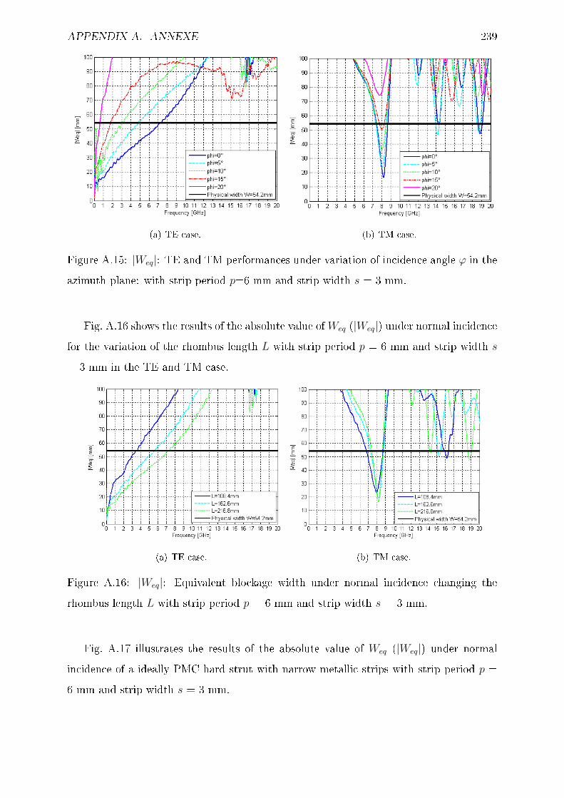
APPENDIX A. ANNEXE 239
(a) TE case. (b) TM case.
Figure A.15: |Weq|: TE and TM performances under variation of incidence angle ϕ in theazimuth plane: with strip period p=6 mm and strip width s = 3 mm.
Fig. A.16 shows the results of the absolute value of Weq (|Weq|) under normal incidencefor the variation of the rhombus length L with strip period p = 6 mm and strip width s
= 3 mm in the TE and TM case.
(a) TE case. (b) TM case.
Figure A.16: |Weq|: Equivalent blockage width under normal incidence changing therhombus length L with strip period p = 6 mm and strip width s = 3 mm.
Fig. A.17 illustrates the results of the absolute value of Weq (|Weq|) under normalincidence of a ideally PMC hard strut with narrow metallic strips with strip period p =6 mm and strip width s = 3 mm.

APPENDIX A. ANNEXE 240
Figure A.17: |Weq|: Equivalent blockage width under normal incidence of a ideally PMChard strut with narrow metallic strips with strip period p = 6 mm and strip width s = 3mm.
Fig. A.18 shows the results of the absolute value of Weq (|Weq|) of a ideally PMC hardstrut under variation of incidence angle ϕ in the azimuth plane: with strip period p = 6mm and strip width s = 3 mm in the TE and TM cases.
(a) TE case. (b) TM case.
Figure A.18: |Weq|: Equivalent blockage width of a ideally PMC hard strut under variationof incidence angle ϕ in the azimuth plane: with strip period p = 6 mm and strip width s
= 3 mm.