Embed Size (px)
Citation preview
Temperature and Time DependentTemperature and Time Dependent Spectroscopy of Luminescent Materials
e
Thomas JüstelMü t U i it f A li d S iMünster University of Applied Sciences
T. Jüstel, University of Applied Sciences Münster, Germany Slide 1
University Siegen @ July 02nd, 2013
Luminescent Materials – Simply Everywhere!Luminescent Materials Simply Everywhere!CRTs Plasma DisplaysLEDs
Fluorescent Lamps EL DisplaysTomographs (CT/PET)
T. Jüstel, University of Applied Sciences Münster, Germany Slide 2
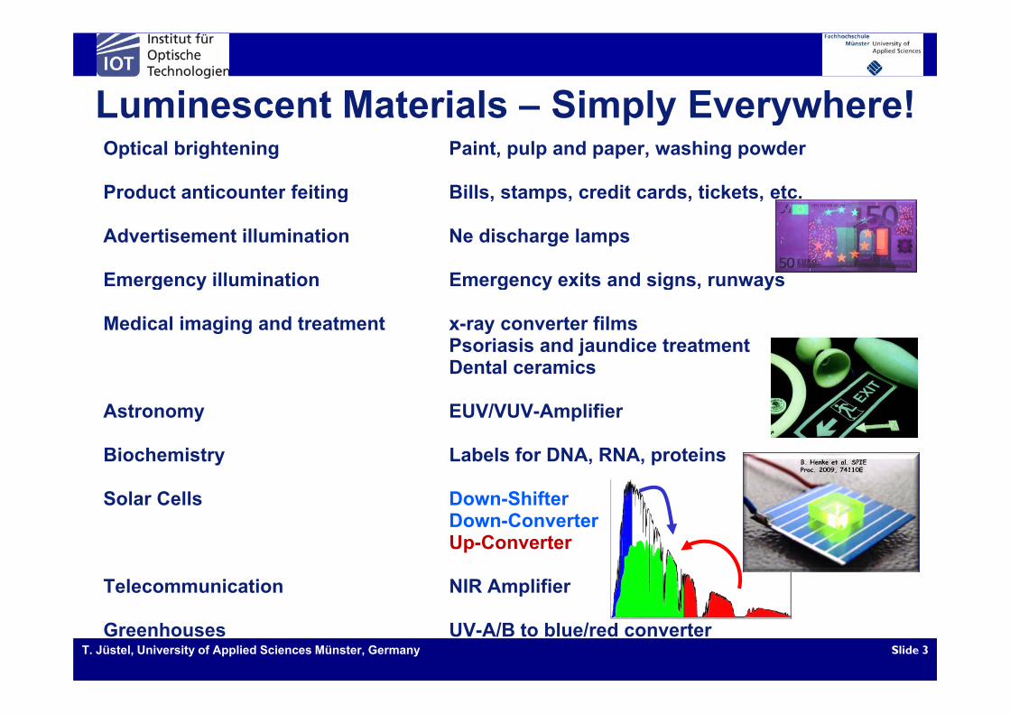
Luminescent Materials – Simply Everywhere!Optical brightening Paint, pulp and paper, washing powder
Product anticounter feiting Bills stamps credit cards tickets etc
Luminescent Materials Simply Everywhere!
Product anticounter feiting Bills, stamps, credit cards, tickets, etc.
Advertisement illumination Ne discharge lamps
Emergenc ill mination Emergenc e its and signs r n a sEmergency illumination Emergency exits and signs, runways
Medical imaging and treatment x-ray converter filmsPsoriasis and jaundice treatmentDental ceramics
Astronomy EUV/VUV-Amplifier
Biochemistry Labels for DNA, RNA, proteins
Solar Cells Down-ShifterDown ConverterDown-ConverterUp-Converter
Telecommunication NIR Amplifier
T. Jüstel, University of Applied Sciences Münster, Germany Slide 3Greenhouses UV-A/B to blue/red converter

OutlineOutline1. Motivation
2. Luminescence Mechanisms
3. Quenching Processes
4. Analytical Access y
5. Examples– Ce3+ activated phosphates and garnetsCe activated phosphates and garnets– Eu2+ activated aluminates and nitrides– Pr3+ activated phosphors– Bi3+ activated VUV to UV converter– Bi activated VUV to UV converter
6. Some Conclusions
T. Jüstel, University of Applied Sciences Münster, Germany Slide 4
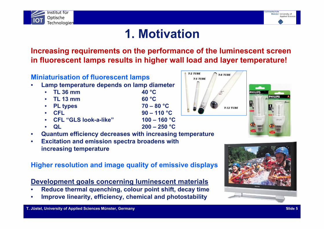
1. Motivation1. MotivationIncreasing requirements on the performance of the luminescent screen in fluorescent lamps results in higher wall load and layer temperature!in fluorescent lamps results in higher wall load and layer temperature!
Miniaturisation of fluorescent lamps• Lamp temperature depends on lamp diameter
• TL 36 mm 40 °C• TL 13 mm 60 °C• PL types 70 – 80 °C• CFL 90 – 110 °CCFL 90 110 C• CFL “GLS look-a-like” 100 – 160 °C• QL 200 – 250 °C
• Quantum efficiency decreases with increasing temperature• Excitation and emission spectra broadens with• Excitation and emission spectra broadens with
increasing temperature
Higher resolution and image quality of emissive displaysHigher resolution and image quality of emissive displays
Development goals concerning luminescent materials• Reduce thermal quenching, colour point shift, decay time
T. Jüstel, University of Applied Sciences Münster, Germany Slide 5
q g p y• Improve linearity, efficiency, chemical and photostability

1. Motivation1. MotivationTremendous advances in LED technology
Luminescent screen
1970(G A )P
2013(Al I G )P (I G )N (Al G )N(Ga,As)P
< 0.1 W< 1.0 lm
< 10 lm/W
(Al,In,Ga)P, (In,Ga)N, (Al,Ga)N0.6 - 5 W> 100 lm
up to 273 lm/W!!!< 10 lm/W< 120 °C
< 100 W/cm2
> 120 K/W
up to 273 lm/W!!!120 – 200 °C
100 – 200 W/cm2
2 12 K/W
T. Jüstel, University of Applied Sciences Münster, Germany Slide 6
> 120 K/WYellow, red, IR
2 – 12 K/WUV-A/B/C, all colors, NIR
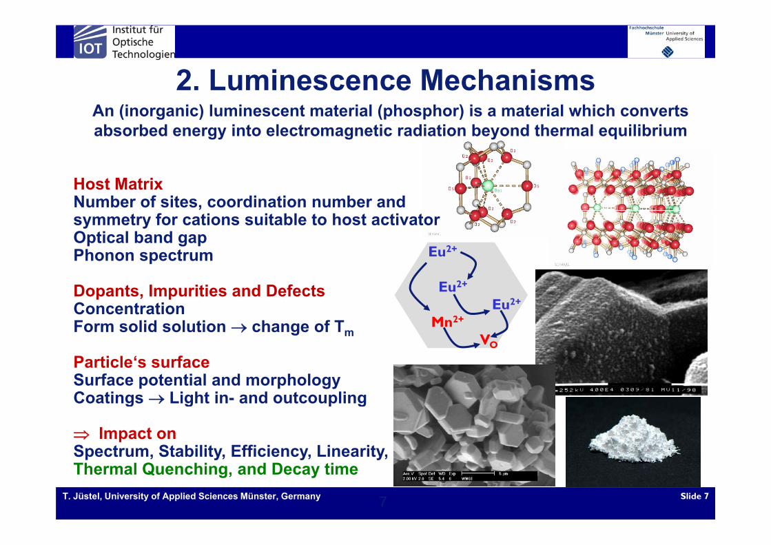
2. Luminescence Mechanisms2. Luminescence MechanismsAn (inorganic) luminescent material (phosphor) is a material which converts absorbed energy into electromagnetic radiation beyond thermal equilibrium
Host MatrixNumber of sites, coordination number andsymmetry for cations suitable to host activatorOptical band gapPhonon spectrum Eu2+
Dopants, Impurities and Defects ConcentrationForm solid solution change of Tm
Eu2+
Eu2+
Mn2+
Vg m
Particle‘s surfaceSurface potential and morphologyCoatings Light in and outcoupling
VO
Coatings Light in- and outcoupling
Impact on Spectrum, Stability, Efficiency, Linearity,
T. Jüstel, University of Applied Sciences Münster, Germany Slide 77
p , y, y, y,Thermal Quenching, and Decay time
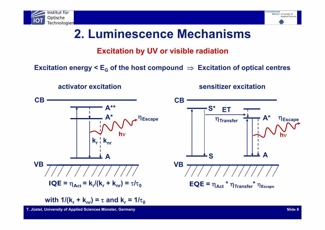
2. Luminescence Mechanisms2. Luminescence MechanismsExcitation by UV or visible radiation
Excitation energy < EG of the host compound Excitation of optical centres
activator excitation sensitizer excitationact ato e c tat o se s t e e c tat o
A*
CBS* ETA**
CB
k
A* A*Transfer
kh
Escape Escape
hknr
AVB
SVB
A
kr
IQE = Act = kr/(kr + knr) = /0 EQE = Act * Transfer* Escape
T. Jüstel, University of Applied Sciences Münster, Germany Slide 8
with 1/(kr + knr) = and kr = 1/0
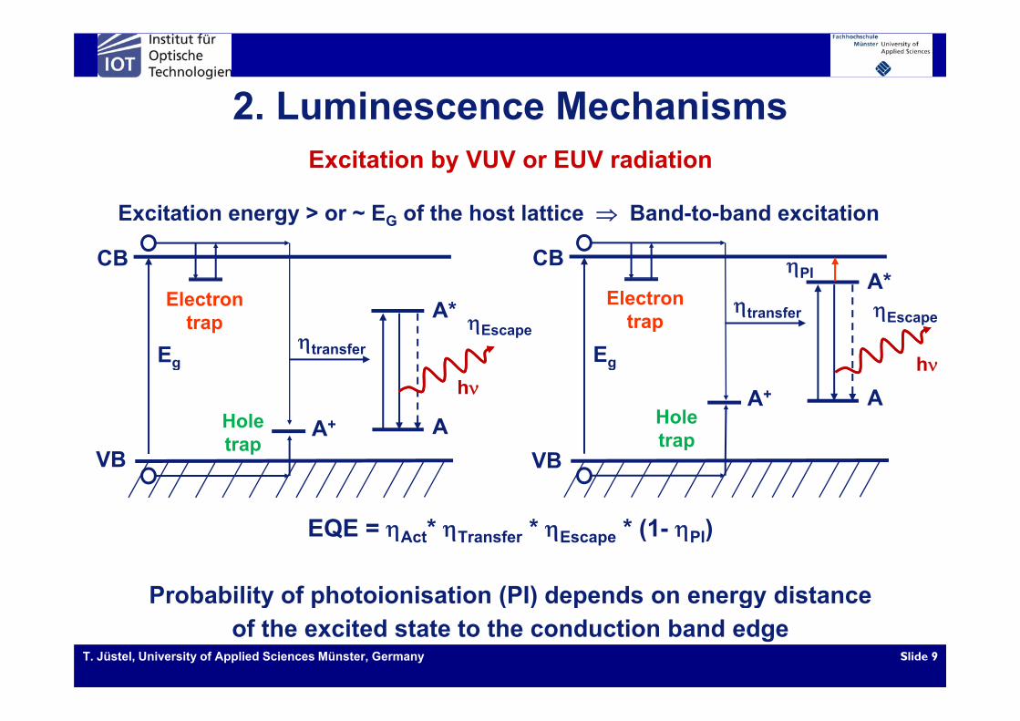
2. Luminescence MechanismsExcitation by VUV or EUV radiation
2. Luminescence Mechanisms
CB
Excitation energy > or ~ EG of the host lattice Band-to-band excitation
CBA*
PI
Eg
Electrontrap
transfer
A*
Eg
transfer
A*Electron
trapEscapeEscape
h
A+
Eg
AA+
Eg
AHoletrap
Holetrap
hh
EQE = * * * (1 )
VB VBtraptrap
EQE = Act* Transfer * Escape * (1- PI)
Probability of photoionisation (PI) depends on energy distance
T. Jüstel, University of Applied Sciences Münster, Germany Slide 9
y p ( ) p gyof the excited state to the conduction band edge
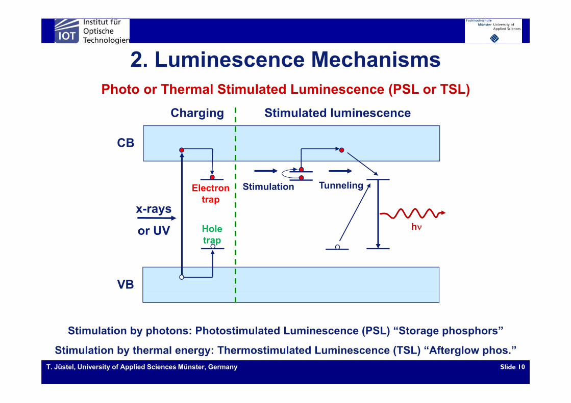
2. Luminescence Mechanisms
Ch i Sti l t d l i
2. Luminescence MechanismsPhoto or Thermal Stimulated Luminescence (PSL or TSL)
Charging Stimulated luminescenceCBCB
Electron trap
Stimulation Tunneling
x-rays
or UV
trap
Hole trap
h
VB
Stimulation by photons: Photostimulated Luminescence (PSL) “Storage phosphors”
T. Jüstel, University of Applied Sciences Münster, Germany Slide 10
Stimulation by thermal energy: Thermostimulated Luminescence (TSL) “Afterglow phos.”
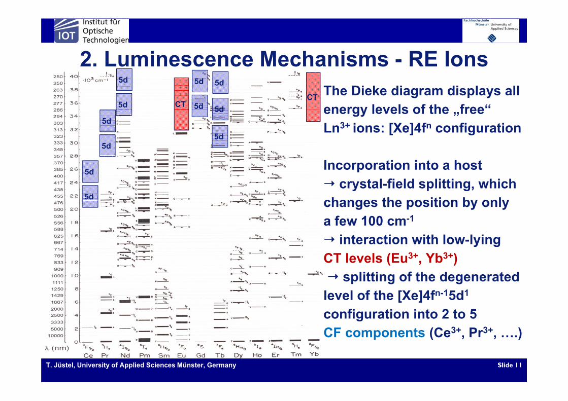
2. Luminescence Mechanisms - RE Ions2. Luminescence Mechanisms RE IonsThe Dieke diagram displays all energy levels of the free“CT
CT
5d
5d
5d
5d
5d
5d energy levels of the „free Ln3+ ions: [Xe]4fn configuration5d
5d
5d
5d
Incorporation into a host crystal-field splitting, whichchanges the position by only
5d
5d changes the position by onlya few 100 cm-1
interaction with low-lyingy gCT levels (Eu3+, Yb3+) splitting of the degeneratedl l f th [X ]4fn 15d1level of the [Xe]4fn-15d1
configuration into 2 to 5CF components (Ce3+, Pr3+, ….)
T. Jüstel, University of Applied Sciences Münster, Germany Slide 11
CF components (Ce , Pr , ….)
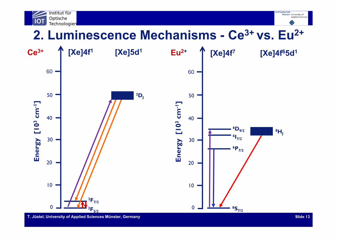
2. Luminescence Mechanisms - Ce3+ vs. Eu2+2. Luminescence Mechanisms Ce vs. EuCe3+ Eu2+[Xe]4f1 [Xe]5d1 [Xe]4f7 [Xe]4f65d1
60 60
cm-1
]
50
40
2DJ
cm-1
]
50
40
rgy
[103
30
40
gy[1
03
30
40
6
6I7/2
6D9/2 8HJ
Ene
r
20 Ene
rg
20
6P7/2
2F
10 10
T. Jüstel, University of Applied Sciences Münster, Germany Slide 12
2F5/2
2F7/20 0 8S7/2

2. Luminescence Mechanisms - Eu2+
crystal field
8H7/2[Xe]4f65d1
2. Luminescence Mechanisms Eu
crystal fieldsplitting
εcentroid Stokes Shift3.0x104
00 c
m-1
6P7/2
cm-1
]
centroidshift
εcfs
2.0x10⁴
se ~
340
0
Ener
gy[c
gas
phas
SS
E
1.0x10⁴
+in
the
g
0 0 [X ]4f7
Eu2+
8 8 8 8
T. Jüstel, University of Applied Sciences Münster, Germany Slide 13
0.0 [Xe]4f7 8S7/28S7/2
8S7/28S7/2
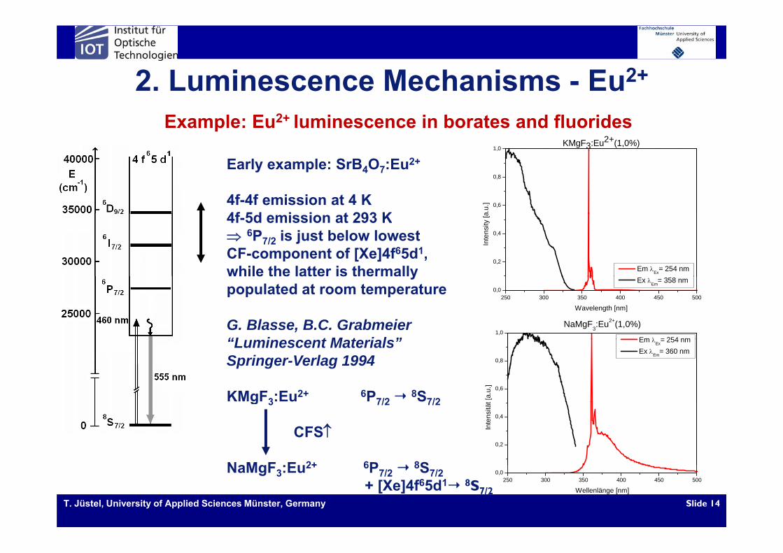
2. Luminescence Mechanisms - Eu2+
Example: Eu2+ luminescence in borates and fluorides1,0
KMgF3:Eu2+(1,0%)
2. Luminescence Mechanisms Eu
0,6
0,8
,
a.u.
]
Early example: SrB4O7:Eu2+
4f-4f emission at 4 K4f 5d i i t 293 K
0,2
0,4
Inte
nsity
[a
Em Ex= 254 nm
4f-5d emission at 293 K 6P7/2 is just below lowestCF-component of [Xe]4f65d1, while the latter is thermally
250 300 350 400 450 5000,0
Wavelength [nm]
Ex Em= 358 nm
1,0NaMgF3:Eu2+(1,0%)
Em = 254 nm
ypopulated at room temperature
G. Blasse, B.C. Grabmeier“L i t M t i l ”
0,6
0,8
t [a.
u.]
Em Ex= 254 nm Ex Em= 360 nm
“Luminescent Materials”Springer-Verlag 1994
KMgF3:Eu2+ 6P7/2 8S7/2
0,2
0,4
Inte
nsitä
tg 3 7/2 7/2
CFS
N M F E 2+ 6P 8S
T. Jüstel, University of Applied Sciences Münster, Germany Slide 14
250 300 350 400 450 5000,0
Wellenlänge [nm]
NaMgF3:Eu2+ 6P7/2 8S7/2+ [Xe]4f65d1 8S7/2
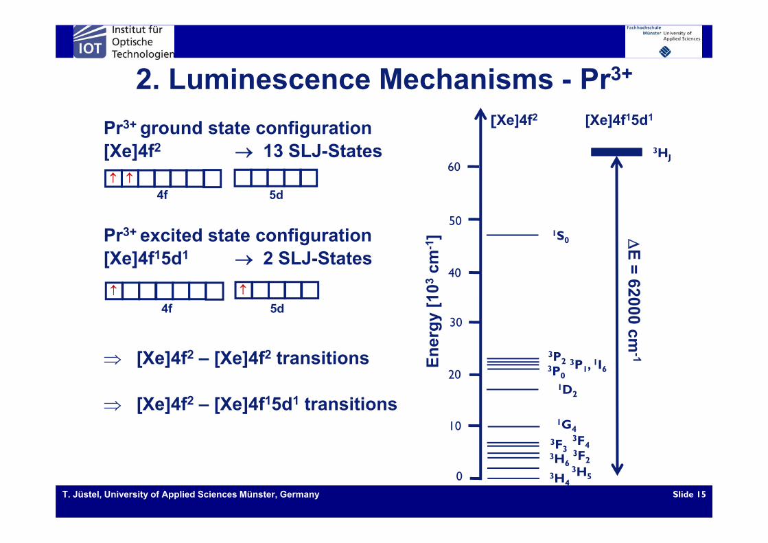
2. Luminescence Mechanisms - Pr3+
Pr3+ ground state configuration[Xe]4f2 13 SLJ States
[Xe]4f2 [Xe]4f15d1
3
2. Luminescence Mechanisms Pr
[Xe]4f2 13 SLJ-States
4f 5d
603HJ
Pr3+ excited state configuration[Xe]4f15d1 2 SLJ-States cm
-1] 1S0
50
40
E =
4f 5d
rgy
[103
c
30
40
= 62000 c
[Xe]4f2 – [Xe]4f2 transitions Ener
1D2
3P23P020
3P1, 1I6
cm-1
[Xe]4f2 – [Xe]4f15d1 transitions
3H
2
1G4
3F
103F3
3F4
T. Jüstel, University of Applied Sciences Münster, Germany Slide 15
3H4
3H5
3H6F2
0
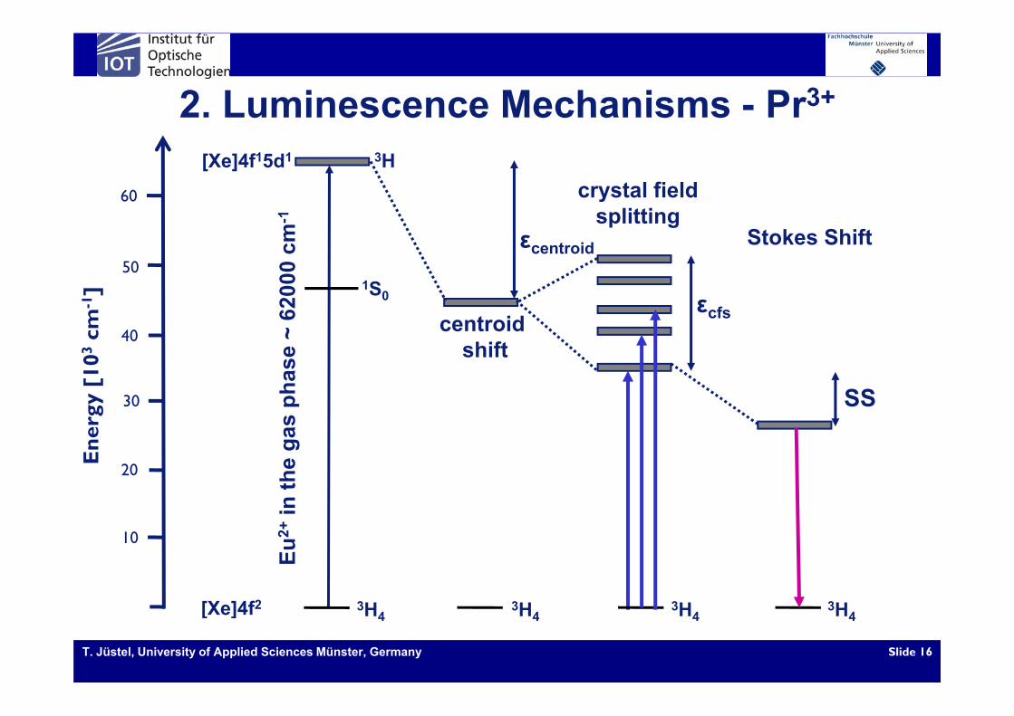
2. Luminescence Mechanisms - Pr3+2. Luminescence Mechanisms Pr
crystal field3H[Xe]4f15d1
60 crystal fieldsplitting
εcentroid Stokes Shift
00 c
m-1
50
60
centroidshift
εcfse
~ 62
00 1S0
03cm
-1]
40
as p
has
SS
ergy
[10
30
in th
e gEn
20
[X ]4f2
Eu2+
3 3 3 3
10
T. Jüstel, University of Applied Sciences Münster, Germany Slide 16
[Xe]4f2 3H43H4
3H43H4
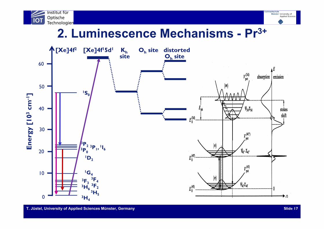
2. Luminescence Mechanisms - Pr3+
60
[Xe]4f2 [Xe]4f15d1 Kh Oh site distorted site Oh site
2. Luminescence Mechanisms Pr
50
60
3cm
-1] 1S0
40
ergy
[10
30
Ene
1D2
3P23P020
3P1, 1I6
3H3H6
1G4
3F2
103F3
3F4
T. Jüstel, University of Applied Sciences Münster, Germany Slide 17
3H4
3H50
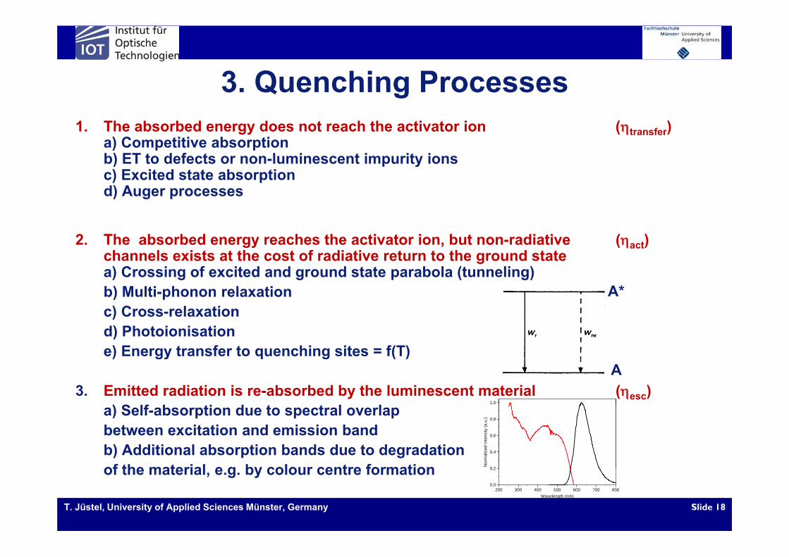
3. Quenching Processes3. Quenching Processes1. The absorbed energy does not reach the activator ion (transfer)
a) Competitive absorptionb) ET to defects or non-luminescent impurity ionsc) Excited state absorptiond) Auger processes
2. The absorbed energy reaches the activator ion, but non-radiative (act)channels exists at the cost of radiative return to the ground statea) Crossing of excited and ground state parabola (tunneling)) g g p ( g)b) Multi-phonon relaxationc) Cross-relaxationd) Photoionisation
A*
e) Energy transfer to quenching sites = f(T)
3. Emitted radiation is re-absorbed by the luminescent material (esc)) S lf b ti d t t l l
1,0
A
a) Self-absorption due to spectral overlap between excitation and emission bandb) Additional absorption bands due to degradation of the material e g by colour centre formation 0 2
0,4
0,6
0,8
Nor
mal
ized
inte
nsity
(a.u
.)
T. Jüstel, University of Applied Sciences Münster, Germany Slide 18
of the material, e.g. by colour centre formation200 300 400 500 600 700 800
0,0
0,2
Wavelength (nm)

3. Quenching ProcessesRelated to the activator (IQE) and to the host matrix (EQE)
3. Quenching Processes
I t l Q t Effi i
CB
Internal Quantum EfficiencyIQE = act
= kr/(kr + knr) = /0
A*
CB /0(Anti proportional to decay time)Decay time (Fluorescence spectrometer)abs
A
Egtransfer External Quantum Efficiency
EQE = Nh(emitted)/N h(absorbed)= transfer* act* esc
act escape
A
VB
A+
transfer act esc(No correlation to decay time!)Emission spectrum (Ulbricht sphere)
Light YieldLY = EQE * abs = EQE*(1-R )(No correlation to decay time!)
T. Jüstel, University of Applied Sciences Münster, Germany Slide 19
( y )Reflection spectrum (Ulbricht sphere)
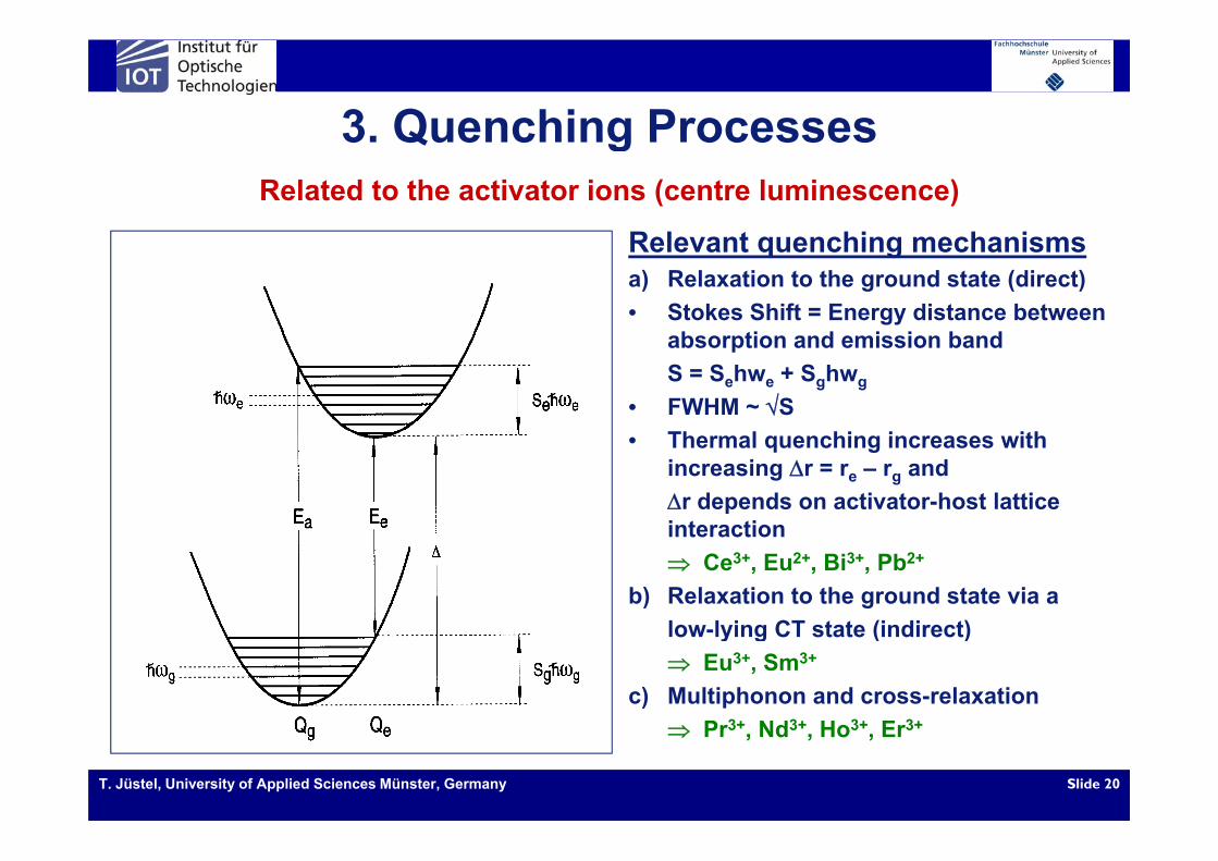
3. Quenching Processes3. Quenching ProcessesRelated to the activator ions (centre luminescence)
R l t hi h iRelevant quenching mechanismsa) Relaxation to the ground state (direct)• Stokes Shift = Energy distance between
b ti d i i b dabsorption and emission bandS = Sehwe + Sghwg
• FWHM ~ S• Thermal quenching increases with
increasing r = re – rg andr depends on activator-host lattice interactioninteraction Ce3+, Eu2+, Bi3+, Pb2+
b) Relaxation to the ground state via a low lying CT state (indirect)low-lying CT state (indirect) Eu3+, Sm3+
c) Multiphonon and cross-relaxation P 3+ Nd3+ H 3+ E 3+
T. Jüstel, University of Applied Sciences Münster, Germany Slide 20
Pr3+, Nd3+, Ho3+, Er3+
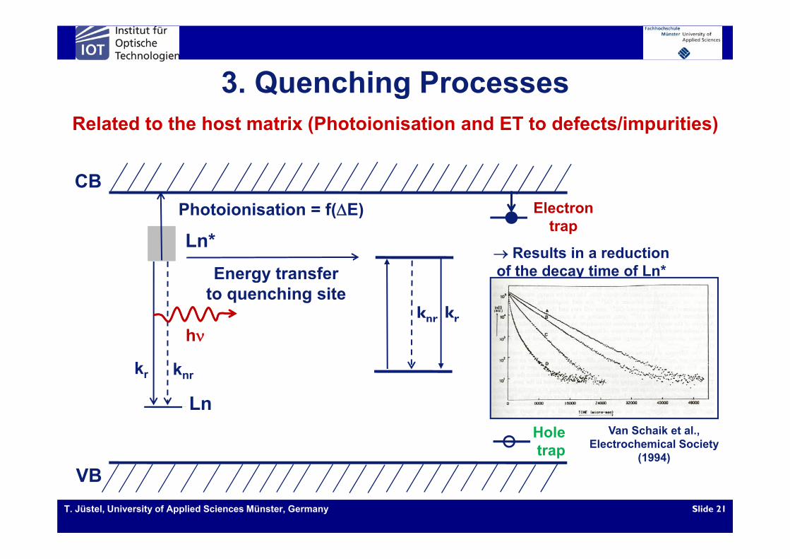
3. Quenching Processes3. Quenching ProcessesRelated to the host matrix (Photoionisation and ET to defects/impurities)
CBElectronPhotoionisation = f(E)
Ln*trap
( )
Energy transfer Results in a reduction of the decay time of Ln*gy
to quenching site
hkrknr
Ln
kr knr
VB
Hole trap
LnVan Schaik et al.,
Electrochemical Society (1994)
T. Jüstel, University of Applied Sciences Münster, Germany Slide 21
VB
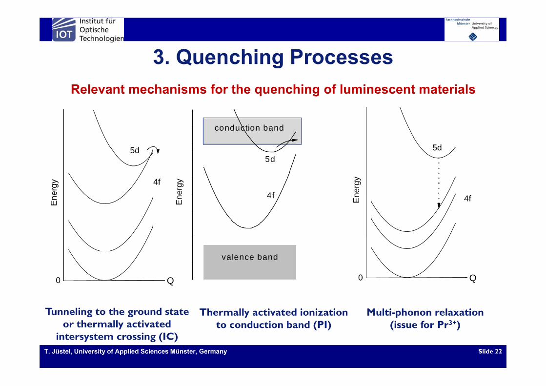
3. Quenching ProcessesRelevant mechanisms for the quenching of luminescent materials
3. Quenching Processes
conduction band
5d 5d
ergy
5d
4fergy
5d
4f
ergy
5d
Ene 4f
Ene En 4f
valence band
0 Q 0 Q0 Q Q
Multi-phonon relaxation(issue for Pr3+)
Thermally activated ionization to conduction band (PI)
Tunneling to the ground stateor thermally activated
T. Jüstel, University of Applied Sciences Münster, Germany Slide 22
(issue for Pr3 )to conduction band (PI)or thermally activated intersystem crossing (IC)
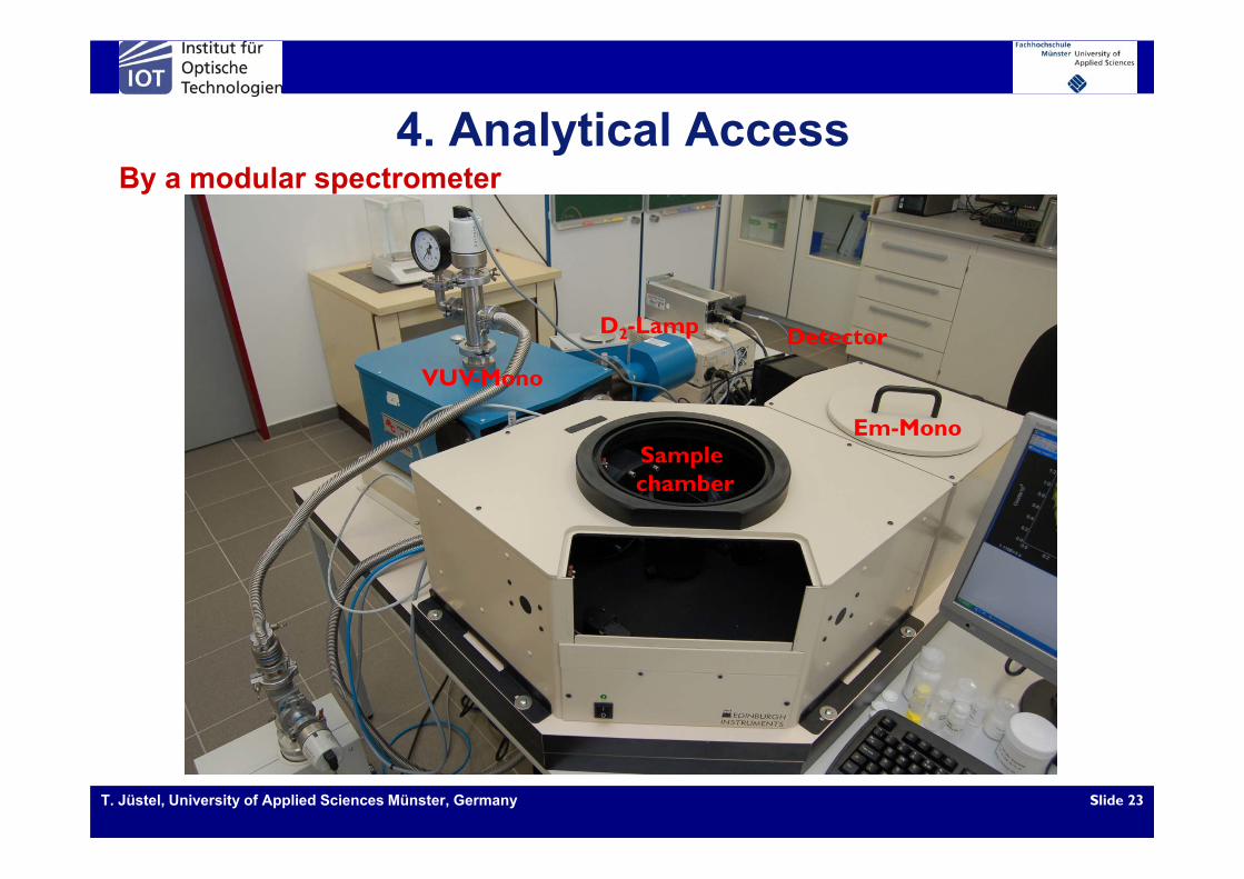
4. Analytical Access4. Analytical AccessBy a modular spectrometer
DetectorD2-Lamp Detector
Em-Mono
VUV-Mono
Sample chamber
T. Jüstel, University of Applied Sciences Münster, Germany Slide 23

4. Analytical AccessTemperature adjustable sample holder
4. Analytical Access
a) Nitrogen cooled cryostat, MicrostatNfrom Oxford Instruments•Temperature range: 77 - 500 K
• Adjustable sample holders accommodate samples up to
8 mm thickness Temperature range: 77 500 K • Fast cool down: 80 K in less than 10 minutes b) 800 K-Heater•Temperature range: 300 - 800 K
• Suitable for reflection, excitation, and emission p g
• Fast heat up: 800 K in less than 5 minutes experiments
T. Jüstel, University of Applied Sciences Münster, Germany Slide 24
MicrostatN (Oxford Instruments) 800 K-Heater
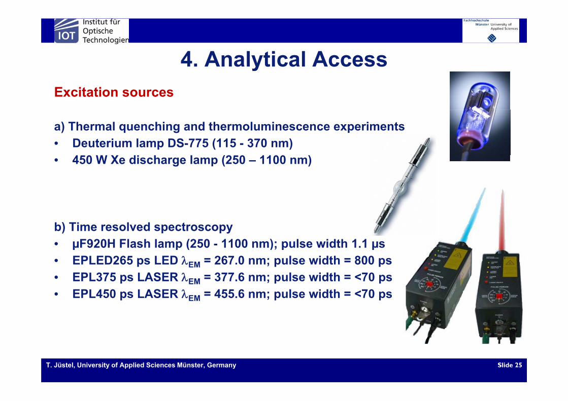
4. Analytical AccessExcitation sources
4. Analytical Access
a) Thermal quenching and thermoluminescence experiments• Deuterium lamp DS-775 (115 - 370 nm) • 450 W Xe discharge lamp (250 – 1100 nm)
b) Time resolved spectroscopy• µF920H Flash lamp (250 - 1100 nm); pulse width 1.1 µsµF920H Flash lamp (250 1100 nm); pulse width 1.1 µs• EPLED265 ps LED EM = 267.0 nm; pulse width = 800 ps• EPL375 ps LASER EM = 377.6 nm; pulse width = <70 ps
EPL450 ps LASER = 455 6 nm p lse idth = <70 ps• EPL450 ps LASER EM = 455.6 nm; pulse width = <70 ps
T. Jüstel, University of Applied Sciences Münster, Germany Slide 25
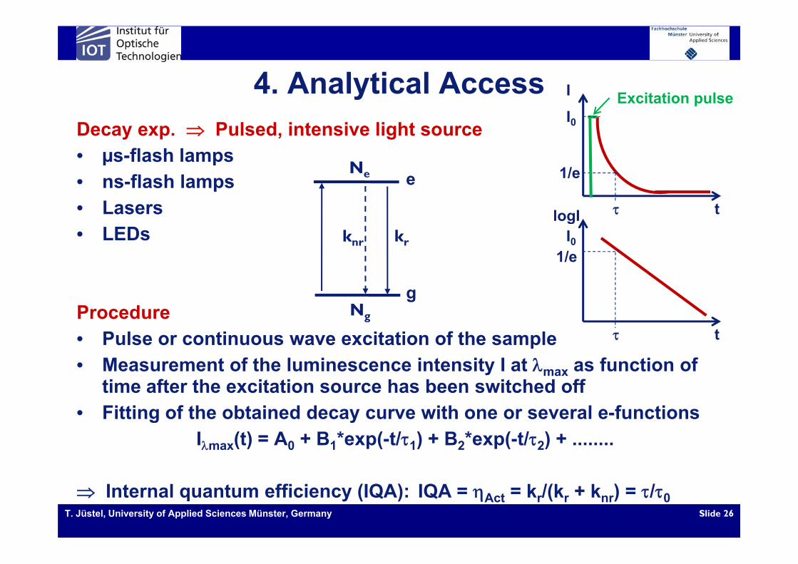
4. Analytical Access I
Decay exp. Pulsed, intensive light source• µs flash lamps
4. Analytical Access I
I0Excitation pulse
• µs-flash lamps• ns-flash lamps• Lasers
eNe
t
1/e
logI• LEDs krknr
logII0
1/e
Procedure• Pulse or continuous wave excitation of the sample
gNg
tp• Measurement of the luminescence intensity I at max as function of
time after the excitation source has been switched off • Fitting of the obtained decay curve with one or several e functions• Fitting of the obtained decay curve with one or several e-functions
Imax(t) = A0 + B1*exp(-t/1) + B2*exp(-t/2) + ........
T. Jüstel, University of Applied Sciences Münster, Germany Slide 26
Internal quantum efficiency (IQA): IQA = Act = kr/(kr + knr) = /0
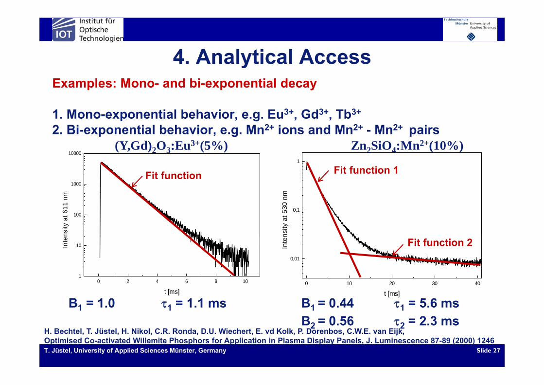
4. Analytical AccessExamples: Mono- and bi-exponential decay
4. Analytical Access
(Y,Gd)2O3:Eu3+(5%) Zn2SiO4:Mn2+(10%)
1. Mono-exponential behavior, e.g. Eu3+, Gd3+, Tb3+
2. Bi-exponential behavior, e.g. Mn2+ ions and Mn2+ - Mn2+ pairs (Y,Gd)2O3:Eu (5%) Zn2SiO4:Mn (10%)
1
m
1000
10000
m
Fit function Fit function 1
0,1
nsity
at 5
30 n
m
100
nsity
at 6
11 n
m
0,01
Inte
n0 2 4 6 8 10
1
10Inte
n
Fit function 2
B1 = 1.0 1 = 1.1 ms B1 = 0.44 1 = 5.6 msB2 = 0.56 2 = 2.3 ms
0 10 20 30 40
t [ms]
0 2 4 6 8 10
t [ms]
T. Jüstel, University of Applied Sciences Münster, Germany Slide 27
B2 0.56 2 2.3 msH. Bechtel, T. Jüstel, H. Nikol, C.R. Ronda, D.U. Wiechert, E. vd Kolk, P. Dorenbos, C.W.E. van Eijk,Optimised Co-activated Willemite Phosphors for Application in Plasma Display Panels, J. Luminescence 87-89 (2000) 1246
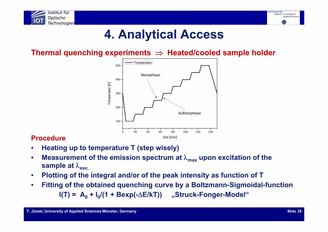
4. Analytical AccessThermal quenching experiments Heated/cooled sample holder
4. Analytical Access
Temperatur
400
500
Messphase
ur [K
]
Temperatur
200
300
Tem
pera
tuAufheizphase
Procedure0 20 40 60 80 100 120 140
100
Zeit [min]
• Heating up to temperature T (step wisely)• Measurement of the emission spectrum at max upon excitation of the
sample at excp exc.• Plotting of the integral and/or of the peak intensity as function of T• Fitting of the obtained quenching curve by a Boltzmann-Sigmoidal-function
I(T) = A + I /(1 + Bexp(-E/kT)) Struck-Fonger-Model“
T. Jüstel, University of Applied Sciences Münster, Germany Slide 28
I(T) = A0 + I0/(1 + Bexp(-E/kT)) „Struck-Fonger-Model

4. Analytical AccessExample: SrGa2S4:Eu Integral and peak intensity as function of temp.
4. Analytical Access
10000
15000 T25 T75 T150 T200T250.u
.] 0,8
1,0 Peak intensityA1 1,0110A2 0,01594x0 179,41
tens
ity
5000
10000 T250 T300 T330
sion
inte
nsity
[a.
0,4
0,6 IntegralA1 0,99900A2 0,002116x0 169 99
dx 26,696
ve e
mis
sion
int
0
5000
Em
iss
0,0
0,2
x0 169,99dx 30,894
y = A2 + (A1-A2)/(1 + exp((x-x0)/dx))
Rel
ativ
exc = 450 nm = 525 nm
450 500 550 600 6500
Wavelength [nm]0 50 100 150 200 250 300 350
0,0
Temperature [°C]
em = 525 nmBaGa2S4:Eu Lit: T1/2 = 210 °C SrGa2S4:Eu Lit: T1/2 = 200 °C Found: T1/2 = 170 °C Strong sample dependenceC G S E Lit T 170 °C
T. Jüstel, University of Applied Sciences Münster, Germany Slide 29
CaGa2S4:Eu Lit.: T1/2 = 170 °C
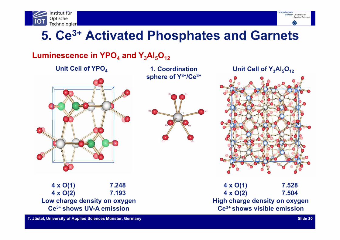
5. Ce3+ Activated Phosphates and Garnets5. Ce Activated Phosphates and GarnetsLuminescence in YPO4 and Y3Al5O12
Unit Cell of YPO4 Unit Cell of Y3Al5O121. Coordinationsphere of Y3+/Ce3+
4 x O(1) 7.2484 x O(2) 7.193
Low charge density on oxygen
4 x O(1) 7.5284 x O(2) 7.504
High charge density on oxygen
T. Jüstel, University of Applied Sciences Münster, Germany Slide 30
Low charge density on oxygenCe3+ shows UV-A emission
High charge density on oxygenCe3+ shows visible emission
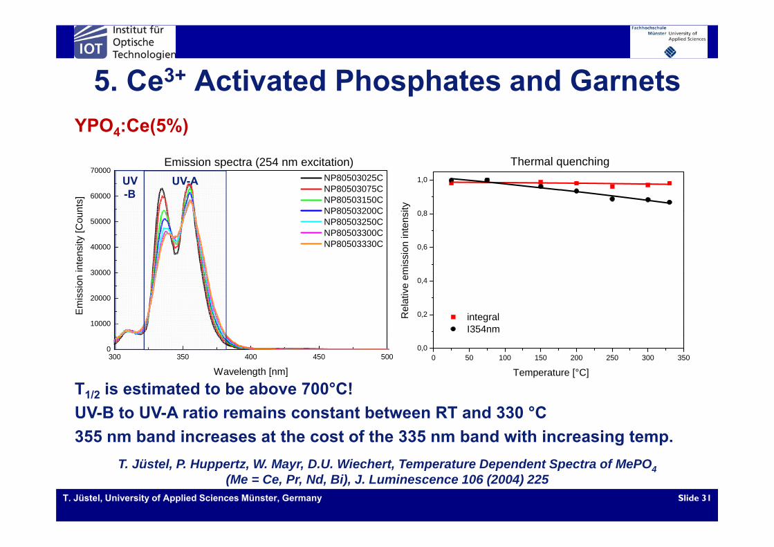
5. Ce3+ Activated Phosphates and GarnetsYPO4:Ce(5%)
5. Ce Activated Phosphates and Garnets
0 8
1,0
Thermal quenching
ity
60000
70000Emission spectra (254 nm excitation)
NP80503025C NP80503075C NP80503150CNP80503200C
nts]
UV-B
UV-A
0,6
0,8
mis
sion
inte
nsi
30000
40000
50000NP80503200C NP80503250C NP80503300C NP80503330C
inte
nsity
[Cou
n
0,2
0,4
integral I354nm
Rel
ativ
e em
10000
20000
30000
Em
issi
on
T1/2 is estimated to be above 700°C!
0 50 100 150 200 250 300 3500,0
Temperature [°C]
300 350 400 450 5000
Wavelength [nm]
1/2
UV-B to UV-A ratio remains constant between RT and 330 °C355 nm band increases at the cost of the 335 nm band with increasing temp.
T Jü t l P H t W M D U Wi h t T t D d t S t f M PO
T. Jüstel, University of Applied Sciences Münster, Germany Slide 31
T. Jüstel, P. Huppertz, W. Mayr, D.U. Wiechert, Temperature Dependent Spectra of MePO4(Me = Ce, Pr, Nd, Bi), J. Luminescence 106 (2004) 225
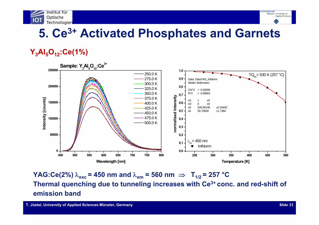
5. Ce3+ Activated Phosphates and Garnets5. Ce Activated Phosphates and GarnetsY3Al5O12:Ce(1%)
200000
250000Sample: Y3Al5O12:Ce3+
250.0 K 275.0 K 300.0 K
0 8
0,9
1,0TQ50= 530 K (257 °C)
Data: DataYAG_IntNormModel: Boltzmann
150000
200000
[cou
nts]
325.0 K 350.0 K 375.0 K 400.0 K 425.0 K 450 0 K 0,5
0,6
0,7
0,8 Chi^2 = 0.00006R^2 = 0.99663 A1 1 ±0A2 0 ±0x0 528.90146 ±2.20442dx 59.70609 ±1.7384d
Inte
nsity
50000
100000
Inte
nsity
450.0 K 475.0 K 500.0 K
0,2
0,3
0,4
norm
alis
e d
450 500 550 600 650 700 750 8000
Wavelength [nm]250 300 350 400 450 500
0,0
0,1
Temperature [K]
Ex= 450 nm IntNorm
YAG:Ce(2%) exc = 450 nm and em = 560 nm T1/2 = 257 °CThermal quenching due to tunneling increases with Ce3+ conc. and red-shift of
T. Jüstel, University of Applied Sciences Münster, Germany Slide 32
emission band
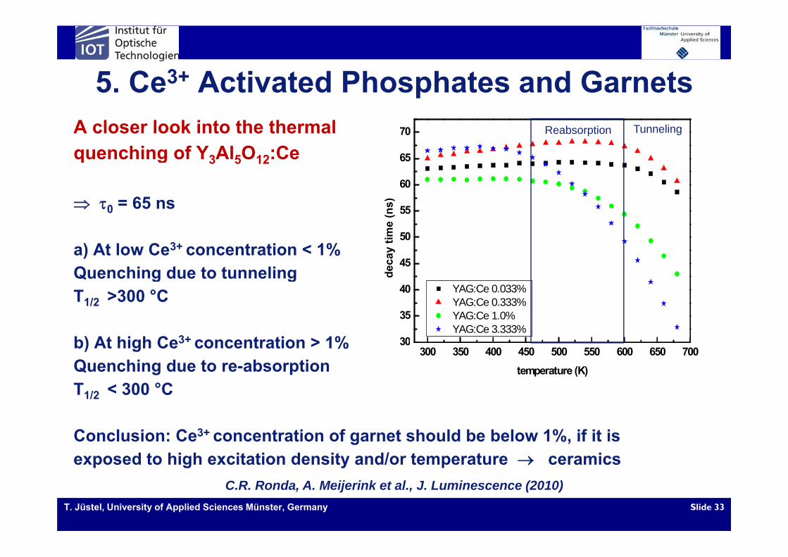
5. Ce3+ Activated Phosphates and GarnetsA closer look into the thermal quenching of Y Al O :Ce
70 Reabsorption Tunneling
5. Ce Activated Phosphates and Garnets
quenching of Y3Al5O12:Ce
0 = 65 ns 55
60
65
(ns)
a) At low Ce3+ concentration < 1%Quenching due to tunneling
45
50
deca
y tim
e (
Que c g due to tu e gT1/2 >300 °C
b) At high Ce3+ concentration > 1% 30
35
40 YAG:Ce 0.033% YAG:Ce 0.333% YAG:Ce 1.0% YAG:Ce 3.333%
b) At high Ce3+ concentration > 1%Quenching due to re-absorptionT1/2 < 300 °C
300 350 400 450 500 550 600 650 70030
temperature (K)
Conclusion: Ce3+ concentration of garnet should be below 1%, if it is exposed to high excitation density and/or temperature ceramics
T. Jüstel, University of Applied Sciences Münster, Germany Slide 33
C.R. Ronda, A. Meijerink et al., J. Luminescence (2010)

5. Ce3+ Activated Phosphates and Garnets5. Ce Activated Phosphates and Garnets
Sample: Lu3Al5O12:Ce3+ Lu3Al5O12:Ce(0.5%)
0,8
0,9
1,0
TQ50= 803 K (530 °C)Data: DataLuAG_IntNormModel: Boltzmann
300000
350000
p 3 5 12
250.0 K 275.0 K 300.0 K 325.0 K
2F5/22F7/2
0,5
0,6
0,7 Chi^2 = 0.00023R^2 = 0.82907 A1 1 ±0A2 0 ±0x0 803.27079 ±68.2418d 145 53693 26 87841
sed
Inte
nsity
150000
200000
250000
ity [c
ount
s]
350.0 K 375.0 K 400.0 K 425.0 K 450.0 K 475 0 K
0,2
0,3
0,4 dx 145.53693 ±26.87841
norm
alis
45050000
100000
150000
Inte
ns 475.0 K 500.0 K
250 300 350 400 450 5000,0
0,1
Temperature [K]
Ex= 450 nm IntNorm
500 550 600 6500
Wavelength [nm]
LuAG:Ce(0.5%) exc = 450 nm and em = 525 nm T1/2 = 530 °CNo decrease in decay time 0 = 54 nsDecrease of the intensity of the 2D - 2F7/2 transition at the cost of the 2D - 2F5/2
T. Jüstel, University of Applied Sciences Münster, Germany Slide 34
Decrease of the intensity of the D F7/2 transition at the cost of the D F5/2transition is due to an increase of re-absorption (esc)
5. Eu2+ Activated Aluminates and Nitrides
Sample: BaMgAl O :Eu2+ 0,8
0,9
1,0Sample: BaMgAl10O17:Eu2+
100
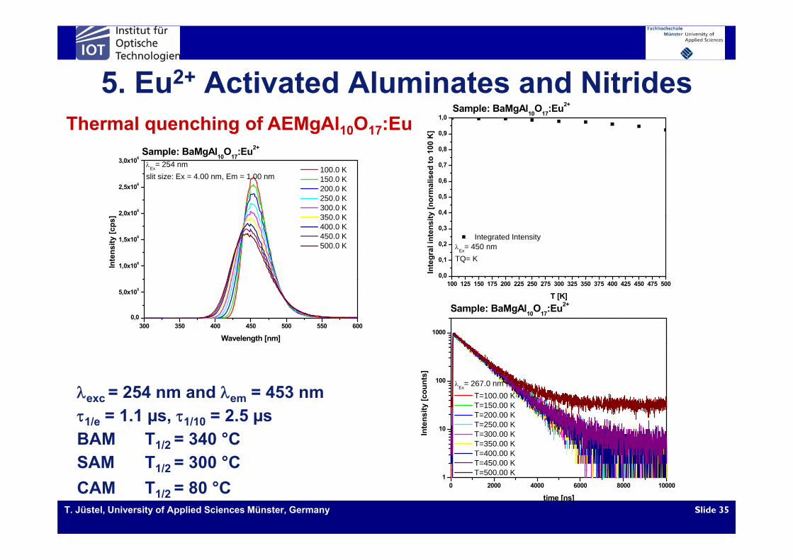
K]Thermal quenching of AEMgAl10O17:Eu
5. Eu Activated Aluminates and Nitrides
2,0x10⁶
2,5x10⁶
3,0x10⁶
Ex= 254 nmslit size: Ex = 4.00 nm, Em = 1.00 nm
Sample: BaMgAl10O17:Eu
]
100.0 K 150.0 K 200.0 K 250.0 K 300.0 K350 0 K
0,4
0,5
0,6
0,7
ty [n
orm
alis
ed to
1
1,0x10⁶
1,5x10⁶
Inte
nsity
[cps
] 350.0 K 400.0 K 450.0 K 500.0 K
0,0
0,1
0,2
0,3
Inte
gral
inte
nsit
Integrated IntensityEx= 450 nmTQ= K
300 350 400 450 500 550 6000,0
5,0x10⁵
Wavelength [nm]
100 125 150 175 200 225 250 275 300 325 350 375 400 425 450 475 500
T [K]
1000
Sample: BaMgAl10O17:Eu2+
exc = 254 nm and em = 453 nm100
y [c
ount
s]
Ex= 267.0 nm T=100.00 KT=150.00 K
1/e = 1.1 µs, 1/10 = 2.5 µsBAM T1/2 = 340 °C SAM T1/2 = 300 °C
10Inte
nsity T 150.00 K
T=200.00 K T=250.00 K T=300.00 K T=350.00 K T=400.00 K T=450.00 KT 500 00 K
T. Jüstel, University of Applied Sciences Münster, Germany Slide 35
1/2
CAM T1/2 = 80 °C 0 2000 4000 6000 8000 100001
time [ns]
T=500.00 K
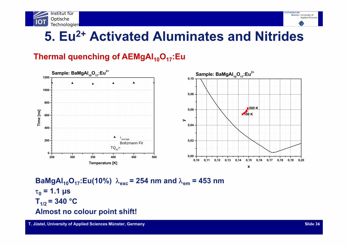
5. Eu2+ Activated Aluminates and NitridesThermal quenching of AEMgAl10O17:Eu
5. Eu Activated Aluminates and Nitrides
1000
1200Sample: BaMgAl10O17:Eu2+
0,08
0,10Sample: BaMgAl10O17:Eu2+
600
800
me
[ns] 0,06
0,08
100 K
500 K
y
200
400
Ti
average
Boltzmann FitTQ50=
0,02
0,04
B M Al O E (10%) 254 d 453
250 300 350 400 450 5000
Temperature [K]0,10 0,11 0,12 0,13 0,14 0,15 0,16 0,17 0,18 0,19 0,20
0,00
x
BaMgAl10O17:Eu(10%) exc = 254 nm and em = 453 nm0 = 1.1 µsT1/2 = 340 °C
T. Jüstel, University of Applied Sciences Münster, Germany Slide 36
Almost no colour point shift!

5. Eu2+ Activated Aluminates and Nitrides5. Eu Activated Aluminates and NitridesDecay of BaMgAl10O17:EuCo as function of excitation energy
1121 nm140 nm160
Results of a bi-exponential fitI = a1 exp(-t/ t1) + a2 exp(-t/ t2)
Decay curves as function of lambda
0,1
160 nm 170 nm180 nm185 nm190 nm
d in
tens
ity
0,3
0,4
0,08
0,1a1(t = 9 s)a2(t = 100 s)
)
0,01Nor
mal
ised
0,20,04
0,06
a 1(t
= 9
s) a2 (t = 100
Ban
0 0010
0,1
0
0,02
120 140 160 180 200 220
s)
nd edge
0,00110 100
Time (s)
120 140 160 180 200 220Excitation wavelength (nm)
Afterglow occurs under band edge excitation!Excitation at band edge results in hole trapping on Co2+ + h+ Co3+
T. Jüstel, University of Applied Sciences Münster, Germany Slide 37
Excitation at band edge results in hole trapping on Co2+ + h+ Co3+
Delayed reactivation: Co3+ + e- (Co2+)* Co2+ Eu2+
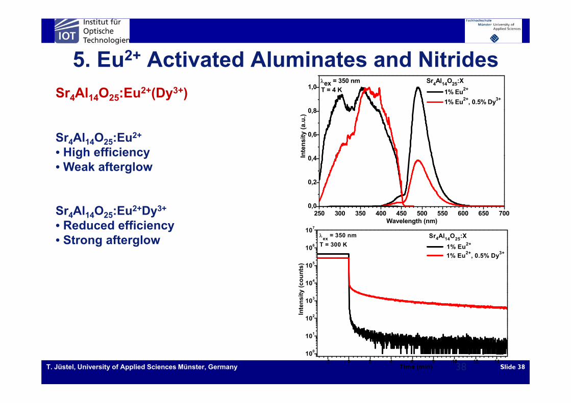
5. Eu2+ Activated Aluminates and NitridesSr4Al14O25:Eu2+(Dy3+)
0 8
1,0 T = 4 Kex = 350 nm Sr4Al14O25:X
1% Eu2+
1% Eu2+, 0.5% Dy3+
5. Eu Activated Aluminates and Nitrides
Sr4Al14O25:Eu2+
• High efficiency 0 4
0,6
0,8
nten
sity
(a.u
.)
High efficiency• Weak afterglow
0,2
0,4I
Sr4Al14O25:Eu2+Dy3+
• Reduced efficiency• Strong afterglow
250 300 350 400 450 500 550 600 650 7000,0
Wavelength (nm)
106
107
Sr4Al14O25:X
1% Eu2+T = 300 Kex = 350 nm
104
105
10 1% Eu2+, 0.5% Dy3+ 1% Eu
ty (c
ount
s)
101
102
103In
tens
it
T. Jüstel, University of Applied Sciences Münster, Germany Slide 3838-2 0 2 4 6 8 10 12 14
100
Time (min)
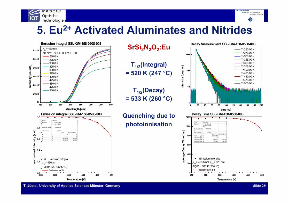
5. Eu2+ Activated Aluminates and NitridesSrSi2N2O2:Eu
1,2x10⁷
Emission integral SSL-GM-158-0508-003Ex= 450 nmslit size: Ex = 4.00, Em = 0.60
250 0 K
1000
T=250.00 K T=275.00 KT 300 00 K
Decay Measurement SSL-GM-158-0508-003
5. Eu Activated Aluminates and Nitrides
T1/2(Integral) = 520 K (247 °C)
6,0x10⁶
8,0x10⁶
1,0x107250.0 K 275.0 K 300.0 K 325.0 K 350.0 K 375.0 K 400.0 Kty
[cou
nts]
100
T=300.00 K T=325.00 K T=350.00 K T=375.00 K T=400.00 K T=425.00 K T=450.00 K
ty [c
ount
s]
T1/2(Decay) = 533 K (260 °C)
0 0
2,0x10⁶
4,0x10⁶
425.0 K 450.0 K 475.0 K 500.0 K
Inte
nsi
10
T=475.00 K T=500.00 K
Inte
nsit
Quenching due tophotoionisation
450 500 550 600 650 700 750 8000,0
Wavelength [nm]
1,0Emission integral SSL-GM-158-0508-003
Model BoltzmannEquation y = A2 + (A1-A2)/(
1 + exp((x-x0)/dx))
0 20 40 60 80 100 120 140 160 180 2001
time [ns]
1200Decay Time SSL-GM-158-0508-003
Model BoltzmannEquation y = A2 + (A1-A2)
/(1 + exp((x x0)/photoionisation
0,6
0,8
Inte
nsity
[a.u
.]
Reduced Chi-Sqr 3,35349E-5
Adj. R-Square 0,99725Value Standard Error
E A1 1 0E A2 0 0E x0 520,38124 1,23589E dx 32,78566 0,98137
600
800
1000
ecay
Tim
e [n
s]
/(1 + exp((x-x0)/dx))
Reduced Chi-Sqr
203,43525
Adj. R-Square 0,9698Value Standard Error
\g(t)\-(average) A1 1185,65373 0\g(t)\-(average) A2 0 0\g(t)\-(average) x0 533,22777 4,57124\g(t)\-(average) dx 27,47347 2,82738
0,2
0,4
Emission IntegralEx= 450 nmTQ50= 520 K (247°C)
Boltzmann Fit
norm
alis
ed
200
400
Emission Intensity Ex= 455.6 nm, Em= 625 nmTQ50 = 533 K (260 °C)
Boltzmann Fit
aver
age
De
T. Jüstel, University of Applied Sciences Münster, Germany Slide 39
250 300 350 400 450 5000,0
Temperature [K]250 300 350 400 450 5000
Temperature [K]
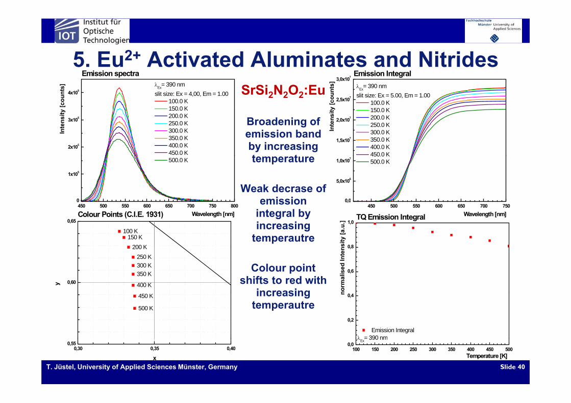
5. Eu2+ Activated Aluminates and Nitrides5. Eu Activated Aluminates and NitridesSrSi2N2O2:Eu4x105
Emission spectraEx= 390 nmslit size: Ex = 4,00, Em = 1.00
100.0 K150.0 K
y
[cou
nts]
2,5x10⁷
3,0x10⁷ Emission IntegralEx= 390 nmslit size: Ex = 5.00, Em = 1.00
100.0 K150 0 Ky
[cou
nts]
Broadening of emission band by increasing t t
2x10⁵
3x10⁵
150.0 K 200.0 K 250.0 K 300.0 K 350.0 K 400.0 K450.0 K
Inte
nsity
1,5x10⁷
2,0x10⁷
150.0 K 200.0 K 250.0 K 300.0 K 350.0 K 400.0 K450.0 K
Inte
nsit
temperature
Weak decrase of emission0
1x10⁵
500.0 K
0,0
5,0x10⁶
1,0x107450.0 K 500.0 K
emission integral by increasing
temperautre
450 500 550 600 650 700 750 8000
Wavelength [nm]450 500 550 600 650 700 750
0,0
Wavelength [nm]0,65
100 K150 K
200 K
Colour Points (C.I.E. 1931)
0 8
1,0TQ Emission Integral
nsity
[a.u
.]
Colour point shifts to red with
increasing0,60
200 K250 K300 K350 K
400 Ky
0,6
0,8
norm
alis
ed In
ten
increasing temperautre
450 K
500 K
0,2
0,4
Emission Integral = 390 nm
n
T. Jüstel, University of Applied Sciences Münster, Germany Slide 40
0,30 0,35 0,400,55
x100 150 200 250 300 350 400 450 500
0,0Ex 390 nm
Temperature [K]
5. Eu2+ Activated Aluminates and Nitrides5. Eu Activated Aluminates and Nitrides
TQ Decay TimeDecay Measurement
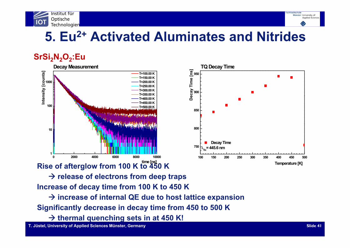
SrSi2N2O2:Eu
900
950
TQ Decay Time
ecay
Tim
e [n
s]
1000
Decay Measurement
nsity
[cou
nts] T=100.00 K
T=150.00 K T=200.00 K T=250.00 K T=300.00 KT=350.00 K
850
De
100Inte
n
T=400.00 K T=450.00 K T=500.00 K
750
800
Decay TimeEx= 445.6 nm
10
Rise of afterglow from 100 K to 450 K release of electrons from deep traps
100 150 200 250 300 350 400 450 500
Temperature [K]0 2000 4000 6000 8000 10000
1
time [ns]
p pIncrease of decay time from 100 K to 450 K increase of internal QE due to host lattice expansion
Significantly decrease in decay time from 450 to 500 K
T. Jüstel, University of Applied Sciences Münster, Germany Slide 41
Significantly decrease in decay time from 450 to 500 K thermal quenching sets in at 450 K!
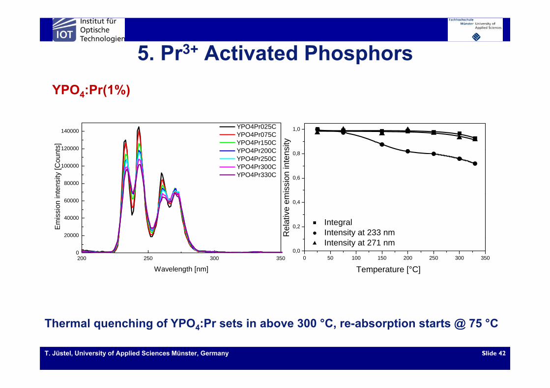
5. Pr3+ Activated PhosphorsYPO4:Pr(1%)
p
1,0
sity
120000
140000 YPO4Pr025C YPO4Pr075C YPO4Pr150CYPO4Pr200C
ts]
0,6
0,8
mis
sion
inte
ns
80000
100000
120000 YPO4Pr200C YPO4Pr250C YPO4Pr300C YPO4Pr330C
nten
sity
[Cou
nt
0,2
0,4
Integral Intensity at 233 nmR
elat
ive
em
20000
40000
60000
Em
issi
on in
0 50 100 150 200 250 300 3500,0
Intensity at 271 nm
Temperature [°C]200 250 300 3500
Wavelength [nm]
Thermal quenching of YPO4:Pr sets in above 300 °C, re-absorption starts @ 75 °C
T. Jüstel, University of Applied Sciences Münster, Germany Slide 42
Thermal quenching of YPO4:Pr sets in above 300 C, re absorption starts @ 75 C
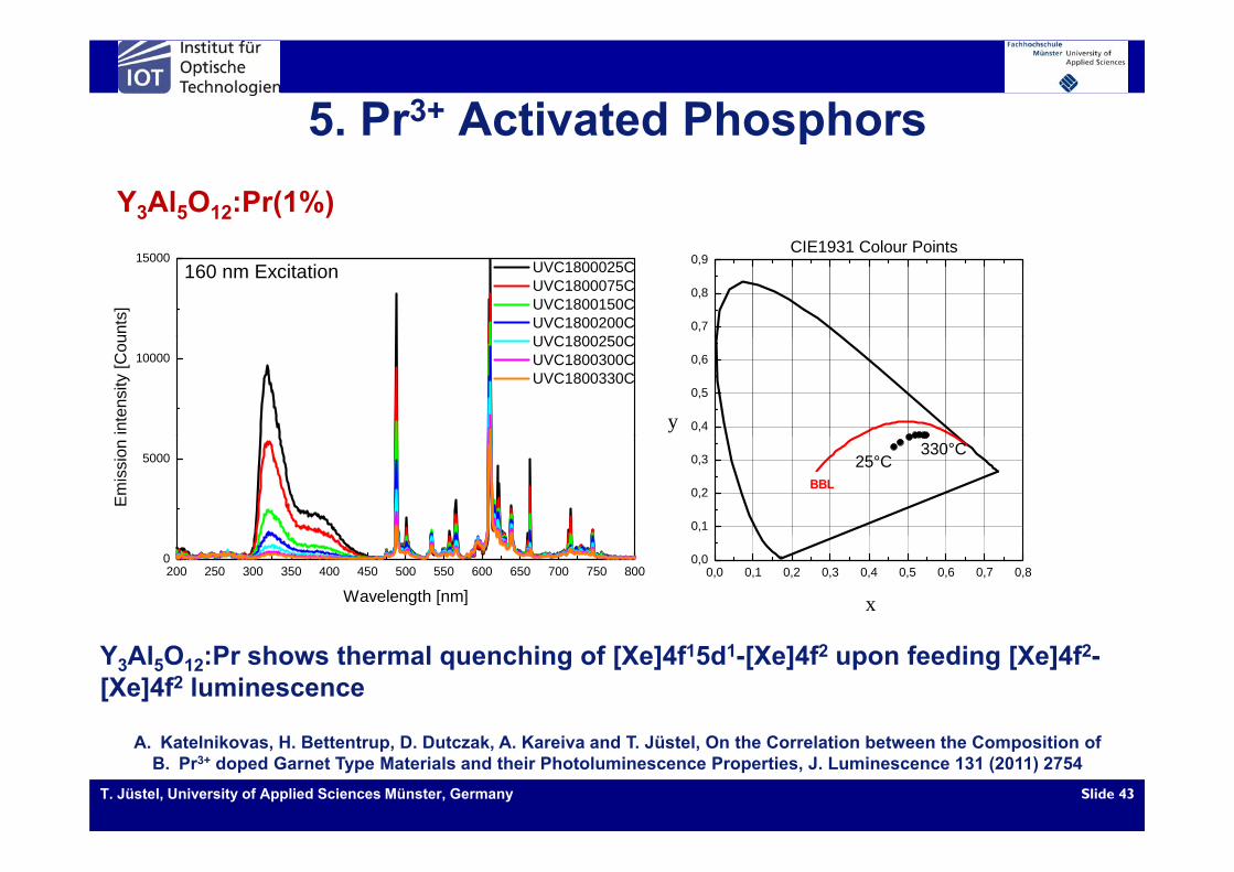
5. Pr3+ Activated PhosphorsY3Al5O12:Pr(1%)
p
15000160 nm Excitation UVC1800025C
UVC1800075C UVC1800150C UVC1800200CUVC1800250Cun
ts]
0,7
0,8
0,9CIE1931 Colour Points
10000UVC1800250C UVC1800300C UVC1800330C
inte
nsity
[Cou
0,4
0,5
0,6
y5000
Em
issi
on
0,1
0,2
0,3330°C
BBL25°C
200 250 300 350 400 450 500 550 600 650 700 750 8000
Wavelength [nm]0,0 0,1 0,2 0,3 0,4 0,5 0,6 0,7 0,8
0,0
x
Y3Al5O12:Pr shows thermal quenching of [Xe]4f15d1-[Xe]4f2 upon feeding [Xe]4f2-[Xe]4f2 luminescence
T. Jüstel, University of Applied Sciences Münster, Germany Slide 43
A. Katelnikovas, H. Bettentrup, D. Dutczak, A. Kareiva and T. Jüstel, On the Correlation between the Composition of B. Pr3+ doped Garnet Type Materials and their Photoluminescence Properties, J. Luminescence 131 (2011) 2754
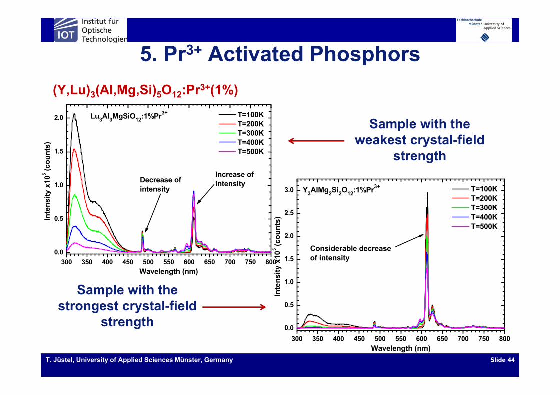
5. Pr3+ Activated Phosphors(Y,Lu)3(Al,Mg,Si)5O12:Pr3+(1%)
p
1.5
2.0 Lu3Al3MgSiO12:1%Pr3+
nts)
T=100K T=200K T=300K T=400KT=500K
Sample with the weakest crystal-field
t th
1.0
1.5
ity x
105 (c
oun T 500K
Increase of intensityDecrease of
intensity
strength
3.0 T=100KT=200K
Y3AlMg2Si2O12:1%Pr3+
0.5Inte
nsi
2.0
2.5
coun
ts)
T=200K T=300K T=400K T=500K
300 350 400 450 500 550 600 650 700 750 8000.0
Wavelength (nm)
Sample ith the1.0
1.5
tens
ity x
105 (c Considerable decrease
of intensity
Sample with the strongest crystal-field
strength 0.0
0.5
Int
T. Jüstel, University of Applied Sciences Münster, Germany Slide 44
300 350 400 450 500 550 600 650 700 750 800Wavelength (nm)

5. Pr3+ Activated Phosphors
1.0
40 Lu3Al3MgSiO12
p(Y,Lu)3(Al,Mg,Si)5O12:Pr3+(1%)
0.5
nteg
ral i
nten
sity
f-f emission d-f emission
Y AlMg Si O Y Al MgSiO
f-f emission d-f emission
30
35
3P23P
Y3Al3MgSiO12
Y3AlMg2Si2O12
0.0
Nor
mal
ized
in Y3AlMg2Si2O12
200
K
228
K
Y3Al3MgSiO12
20
25
P01D2
y (x
103 c
m-1
)
1.0
gral
inte
nsity
f-f emissiond-f emission
f-f emissiond-f emission 10
153H6
Ene
rgy
0.5
233
K
Lu3AlMg2Si2O12
Nor
mal
ized
inte
g d f emission
277
K
Lu3Al3MgSiO12
d f emission
5
103H4
100 150 200 250 300 350 400 450 5000.0
N
Temperature (K)100 150 200 250 300 350 400 450 500
Temperature (K)
0r'0r0
Energy states of the [Xe]4f2 configuration of Pr3+ are efficiently populated with increased temperature Therefore thermal quenching
T. Jüstel, University of Applied Sciences Münster, Germany Slide 45
populated with increased temperature. Therefore thermal quenching sets in at relatively high temperatures
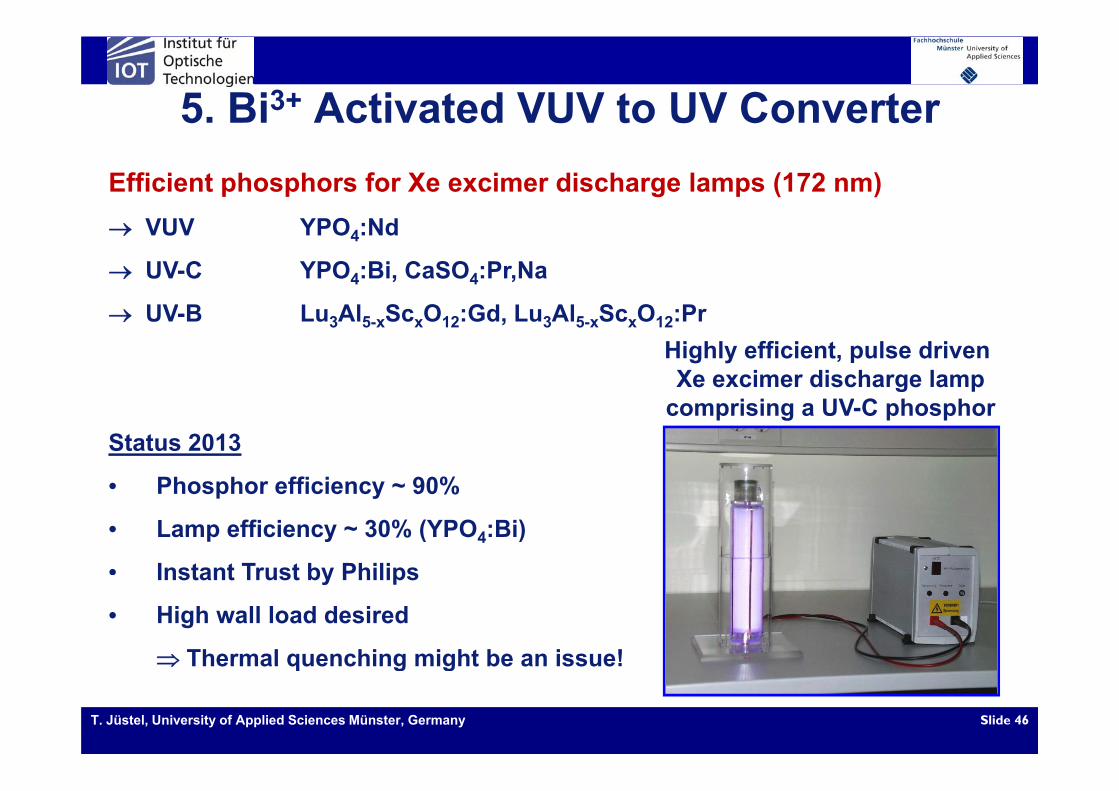
5. Bi3+ Activated VUV to UV ConverterEfficient phosphors for Xe excimer discharge lamps (172 nm) VUV YPO4:Nd
UV-C YPO4:Bi, CaSO4:Pr,Na
UV B L Al S O Gd L Al S O P UV-B Lu3Al5-xScxO12:Gd, Lu3Al5-xScxO12:PrHighly efficient, pulse driven Xe excimer discharge lamp
Status 2013
• Phosphor efficiency ~ 90%
comprising a UV-C phosphor
• Phosphor efficiency ~ 90%
• Lamp efficiency ~ 30% (YPO4:Bi)
• Instant Trust by PhilipsInstant Trust by Philips
• High wall load desired
Thermal quenching might be an issue!
T. Jüstel, University of Applied Sciences Münster, Germany Slide 46
Thermal quenching might be an issue!
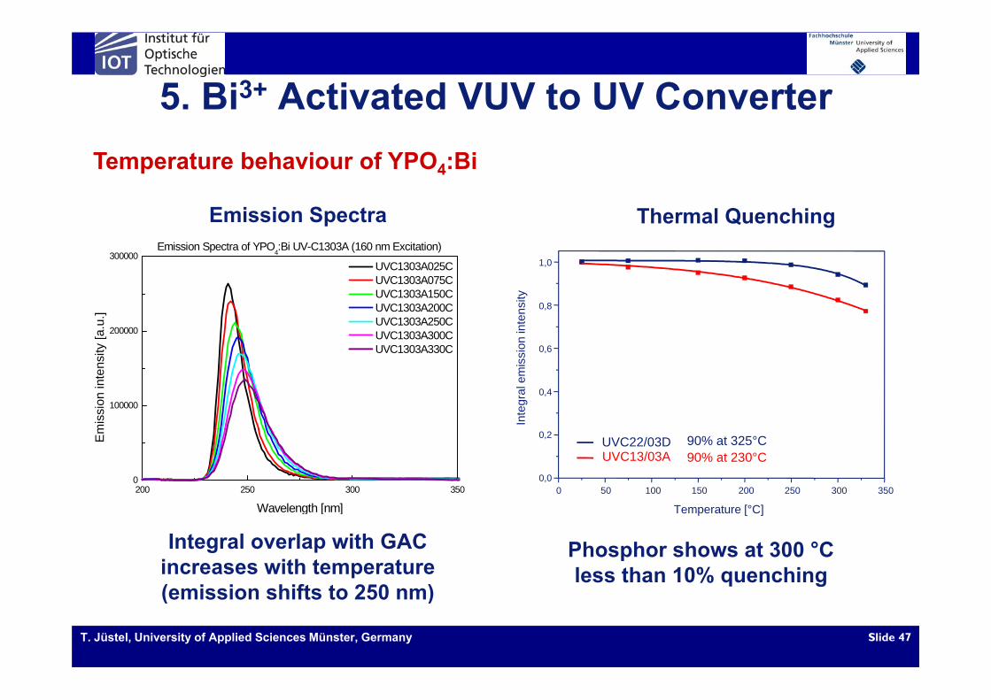
5. Bi3+ Activated VUV to UV ConverterTemperature behaviour of YPO4:Bi
1,0
Thermal QuenchingEmission Spectra
300000Emission Spectra of YPO4:Bi UV-C1303A (160 nm Excitation)
UVC1303A025C
0 6
0,8
on in
tens
ity
200000
UVC1303A075C UVC1303A150C UVC1303A200C UVC1303A250C UVC1303A300CUVC1303A330Cty
[a.u
.]
0,4
0,6
Inte
gral
em
issi
100000
UVC1303A330C
mis
sion
inte
nsit
0 50 100 150 200 250 300 3500,0
0,2
Temperature [°C]
UVC22/03DUVC13/03A
90% at 325°C90% at 230°C
200 250 300 3500
Em
Wavelength [nm] Temperature [ C]
Integral overlap with GACincreases with temperature(emission shifts to 250 nm)
Phosphor shows at 300 °Cless than 10% quenching
Wavelength [nm]
T. Jüstel, University of Applied Sciences Münster, Germany Slide 47
(emission shifts to 250 nm)
6. Some Conclusions6. Some ConclusionsTemperature dependent spectroscopy is a powerful tool to study • Efficiency decrease with temperature i e Final device performance• Efficiency decrease with temperature, i.e. Final device performance
since modern fluorescent light sources operate at elevated temperatureC l i hif i h• Colour point shift with temperature
• Peak broadening and extent of re-absorption
Time dependent spectroscopy is a powerful tool to study • Determine internal quantum efficiency (IQE)• Energy transfer processes to defect sites• Quenching processes due to photoionisation and to diminish them• Quenching processes due to photoionisation and to diminish them
by quenching due to re-absorption
T. Jüstel, University of Applied Sciences Münster, Germany Slide 48
6. Some Conclusions6. Some Conclusions Causes of thermal quenching of a luminescence process
- Tunneling to the ground state = f(Stokes Shift)- Multiphonon relaxation = f(phonon frequency)
Cross relaxation = f(activator distance)- Cross-relaxation = f(activator distance)- ET to defects = f(activator distance)- Photoionisation = f(energy distance to CB)
Measures to reduce thermal quenching- Low activator concentration- Low r = re – rg- Large distance between energy of the excited state and the conduction band edgeg- Low conc. of intrinsic defects and thus high crystallinity- Low conc. of extrinsic defects and thus low impurity level- Energy depletion between ground and excited state level by
T. Jüstel, University of Applied Sciences Münster, Germany Slide 49
Energy depletion between ground and excited state level by centroid shift
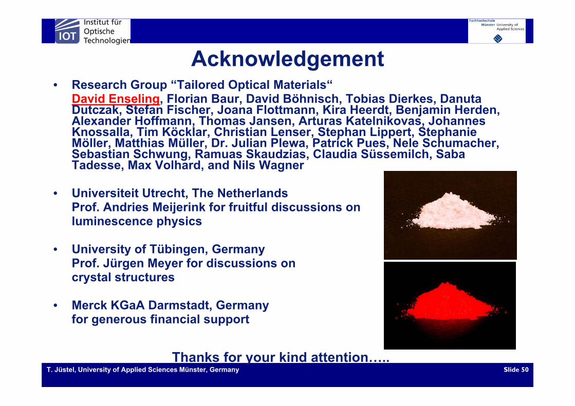
AcknowledgementAcknowledgement• Research Group “Tailored Optical Materials“
David Enseling, Florian Baur, David Böhnisch, Tobias Dierkes, DanutaDutczak Stefan Fischer Joana Flottmann Kira Heerdt Benjamin HerdenDutczak, Stefan Fischer, Joana Flottmann, Kira Heerdt, Benjamin Herden, Alexander Hoffmann, Thomas Jansen, Arturas Katelnikovas, Johannes Knossalla, Tim Köcklar, Christian Lenser, Stephan Lippert, Stephanie Möller, Matthias Müller, Dr. Julian Plewa, Patrick Pues, Nele Schumacher, Sebastian Schwung, Ramuas Skaudzias, Claudia Süssemilch, SabaSebastian Schwung, Ramuas Skaudzias, Claudia Süssemilch, Saba Tadesse, Max Volhard, and Nils Wagner
• Universiteit Utrecht, The NetherlandsP f A d i M ij i k f f itf l di iProf. Andries Meijerink for fruitful discussions on luminescence physics
• University of Tübingen Germany• University of Tübingen, GermanyProf. Jürgen Meyer for discussions on crystal structures
• Merck KGaA Darmstadt, Germanyfor generous financial support
T. Jüstel, University of Applied Sciences Münster, Germany Slide 50Thanks for your kind attention…..