Embed Size (px)
Citation preview

Tellurium and zinc doping in In0.32Ga0.68P layers grown by liquidphase epitaxyChyuanWei Chen and MengChyi Wu Citation: J. Appl. Phys. 70, 5040 (1991); doi: 10.1063/1.349009 View online: http://dx.doi.org/10.1063/1.349009 View Table of Contents: http://jap.aip.org/resource/1/JAPIAU/v70/i9 Published by the American Institute of Physics. Related ArticlesTb3+-Yb3+ cooperative down and up conversion processes in Tb0.81Ca0.19F2.81:Yb3+ single crystals J. Appl. Phys. 110, 123527 (2011) H2O and D2 mixtures under pressure: Spectroscopy and proton exchange kinetics J. Chem. Phys. 135, 174508 (2011) Note: A novel method for in situ loading of gases via x-ray induced chemistry Rev. Sci. Instrum. 82, 106102 (2011) Barrier height and tunneling aspects in (110) CrO2 with its natural barrier J. Appl. Phys. 110, 053708 (2011) Theoretical investigation of resonance Raman scattering of dye molecules absorbed on semiconductor surfaces J. Chem. Phys. 135, 044108 (2011) Additional information on J. Appl. Phys.Journal Homepage: http://jap.aip.org/ Journal Information: http://jap.aip.org/about/about_the_journal Top downloads: http://jap.aip.org/features/most_downloaded Information for Authors: http://jap.aip.org/authors
Downloaded 16 Jan 2012 to 140.114.195.186. Redistribution subject to AIP license or copyright; see http://jap.aip.org/about/rights_and_permissions

BeQlurium and zinc doping in In ,-,32Gia,,68P layers grown by liquid-phase epitaxy
Chyuan-Wei Chen and Meng-Chyi Wu Research Institute of Electrical Engineer& National Tsing Hua University, Hsinchu, Taiwan 30043, Republic of China
(Received 3 June 199 1; accepted for publication 29 July 1991)
Ino.s2Gac6sP epitaxial layers doped with Te and Zn were grown on (100) GaA~s.~iP,,~s epitaxial substrates by liquid-phase epitaxy using a supercooling method. The electrical properties of doped layers were determined by C-V measurements at 300 K. Room- temperature carrier concentrations ranging from 9 X lOi to 2 X 1018 cm - 3 for n-type and from 3 X 10¹⁶ to 6X 1018 cm- 3 for p-type dopants are obtained reproducibly. The full width at half maximum value of the 300 K photoluminescent spectrum increases with carrier concentration for Te- and Zn-doped layers. The relative intensity of 300-K photoluminescent peak presents the maximum values at 1 x lOI and 6~ 10” cm -’ for electron and hole concentrations, respectively. The 100-K photoluminescent spectra show three distinctive peaks and their relative intensities change with hole concentrations. Finally, the relationship between the acceptor ionization energy and hole concentration is described.
I. INTRODUCTION
One of the major topics in the field of light sources is the development of visible light-emitting devices for appli- cation to optical communications through plastic fibers and optical information processing systems such as optical disk memories and audio/video disk equipments. Shorten- ing the emission wavelength is expected to be advantageous for obtaining small focused spots and highly luminous light sources for human vision.
Indium gallium phosphide (Ini _ ,Ga,P) ternary com- pound has received increased attention recently because of its direct bandgap extending up to 2.2 eV (x-0.74) at 300 K and offers, in principle, an opportunity of fabricating efficient light emitters in the red to green region of the visible spectrum.“2 It can be grown on commercial GaAs,,,6,Po.39 epitaxial substrates with exact lattice match at a composition of 68% GaP and a band gap of about 2.17 eV (570 nm in wavelength) .3 It is also a key material for AlInP/InGaP/AlInP, InGaP/AlInGaP/InGaP, InGaP/ InGaAsP/InGaP, and InGaP/AlGaAsP/InGaP hetero- structure visible laser systems. In fabricating laser diodes and light-emitting diodes (LEDs) consisting of InGaP lay- ers, the material must be successfully doped with donor and acceptor impurities. Although InGaP LEDs or laser diodes fabricated on GaAsP substrates by liquid-phase ep- itaxy (LPE)@ or vapor-phase epitaxy (VPE)9*10 have been reported, there are only a few reports on their doping properties. Fujimoto et al. ‘I reported the doping properties of Te and Zn in I~.2~G~.7~Aso,o~Po.95 (Es-2.17 eV) grown on GaAso.61Po,39 substrates by LPE, and concluded that they have the segregation coefficients of 0.009 and 0.035, respectively. Kato et aZ.‘2f’3 reported the transport and photoluminescence properties in solution grown poly- crystalline Ini _ XGaXP doped with Zn. The hole mobilities measured at 300 K were 10-50 cm2/Vs with hole concen- trations of 10’7-10’8 cmB3. But there are no detailed re- ports on the electrical and photoluminescent properties of
Te- and Zn-doped InGaP epitaxial layers grown on ( 100) GaAso,61Po.39 substrates by LPE.
In this paper, we report the doping properties of tellu- rium and zinc in Ine32GaeesP layers grown at 800 “C by a LPE supercooling technique with a supersaturation of 10 “C. Their electrical and optical properties are examined. Various luminescence bands involving donors and accep- tors are identified, and the Zn ionization energy values are deduced from the data.
II. EXPERIMENT
In1 _ ,Ga,P epitaxial layers were grown by LPE using a graphite slider boat. The substrates were GaAso.61Po.39 commercial epitaxial wafers grown by VPE on Si-doped (100) GaAs substrates 2” off towards (110). A --O-pm- thick graded composition of GaAsP layer is used between GaAs and GaA~e.6iP~,~~ layer to avoid large lattice mis- match. The surface GaAso.6i o.39 P layer is 4.0~pm-thick and n doped to 7X 10’” cm - 3 with Te. The In melt was first baked at 900 “C in a purified H2 flow of 500 Wmin for 10 h. After the baking process, 20.2 mg of InP and 12.7 mg of Gap, both polycrystalline, and an appropriate amount of dopant were added to the 3-g In prebaked melt to form the growth solution with a liquid temperature of - 8 10 “C. In this study, Te and Zn were used as n- and p-type dopants, respectively. High-purity tellurium ( 6-9’s) chunks were used because of its low vapor pressure. In order to control the hole concentration accurately, In-l % Zn wires were used in our study. The doped epitaxial layers were grown by means of supercooling technique with - 10 “C! supersat- uration, which is the best growth condition determined previously.i4 The thickness of InGaP epitaxial layers grown during a fixed growth period of 5 min was typically 4 pm.
Capacitance-voltage (C-V) and photoluminescence (PL) measurements were carried out to characterize Te- or Zn-doped Ine3zGac&gP layers. Details of growth condi-
5040 J. Appl. Phys. 70 (9), 1 November 1991 0021-8979/91/095040-05$03.00 @ 1991 American institute of Physics 5040
Downloaded 16 Jan 2012 to 140.114.195.186. Redistribution subject to AIP license or copyright; see http://jap.aip.org/about/rights_and_permissions

tions and characterization techniques were given elsewhere.i4>15
Ill. RESULTS AND DISCUSSIONS
For all the Te- and Zn-doped Ine3zGae6sP samples, the surface morphology is very shiny and flat but with a so-called cross-hatched-pattern surface inherited from the original misfit dislocations introduced during the graded layer growth of GaAsP on the GaAs substrate. The inter- face between epitaxial and GaAso.61Po.39 substrate is also flat and free from inclusions. Lattice mismatch between the epitaxial layers and GaAsP substrates normal to the wafer surface of the doped samples is controlled to be within + 0.15-0.20% which can result in the best layer quality.14
Figure 1 shows the room-temperature carrier concen- trations (n and p) of Te- and Zn-doped Ines2Gae6gP layers grown on G~As~.~~P~.~~ substrates versus Te and Zn mole fractions in growth solutions, & and XL,, respectively. The carrier concentrations increase linearly above 10” cm-s as both dopant mole fractions in the solutions are increased. It is clear that high doping concentrations in excess of lOI cm - 3 can easily be obtained for both n- and p-type materials. In the range studied, 7.6~ 10 - ’ <X& < 2.1 X 10 - 3, the electron concentration increases from
9~ lOI to 2~ 1018 cm- 3. When X& is increased further, the electron concentration saturates at a value near 2 X lOI cmm3. In the range 2~1O-‘<Xh<2~10-“, the hole concentration increases linearly from 3 X 10¹⁶ to 5X 10¹⁸ cmV3. When XL* is increased beyond 2X 10 - 3, the hole concentration saturates at a value near 6 x lo’* cm - 3. The segregation coefficient K of dopant in Ins~zGas&gP at 800 “C is estimated by least-square method using the equation’”
,r-l’SY~ ’ ’ II’ll’ ’ ’ ““I I I Illlllj
; ‘;,-Jo~z~~o;~ ;
l- /4 p/K,,=O.O19
0 Te -doped
l Zn -doped
I 16 -’ 1111111’ 1 I I llglT’ I I I11111
10 ,65 Id’ lci3 Id”
Te OR Zn MOLE FRACTION IN GROWTH SOLUTION, Q
XT* Q
OR X2”
FIG. 1. The room-temperature carrier concentrations (n and p) of Te- and Zn-doped I~,,J~GQJ~P layers grown on G~As~,~~P~,J~ substrates vs Te and Zn mole fractions in growth solutions, A& and XL,, respectively.
I -L- 5300 5500 5700 5900 6100 6:
WAVELENGTH ( % 1
FIG. 2. 300- and 16-K photoluminescent spectra of Te-doped I%,32G%.68P layer grown on GaAsP substrate with an electron concen- tration of 7 X 10” cm - 3. The intensities are normalized to the same value.
K= X”/X’= Na28X1,
where X” and Xl are the mole fractions of dopant in the epitaxial layer and growth solution, respectively, N is the donor or acceptor concentration, and a0 is the lattice con- stant of Ines,Gae6sP and a0 = 5.571 A.3~ The segregation coefficients of Te (KTe) and Zn (Kz,) are calculated to be 0.019 and 0.050, respectively, assuming that all dopants are ionized. The calculated value of KTc is larger than the pre- viously reported value of 0.009 for Ine2,Gae74Aso.osPo,9s grown on GaAso.6iPe.39 (Ref. 11) and near to the previ- ously reported value of 0.015 for Ino,sGaesP grown on GaAs.” Our Kz,, value is slightly larger than the reported value of 0.035 for Zn-doped Ine26Gao.74Aso.osPa95 layers” and much smaller than the value of 0.18 for Zn-doped IncsGao.sP layers.” This difference may be caused by the layer composition and residual impurity concentration dif- ferences. In our study, the background electron concentra- tion of the undoped (n-type) I&~32Gac&gP epitaxial layers was about 1 X 10¹⁶ cme3 or below.14
Typical 300- and 16-K PL spectra of a Te-doped Ino.32Gae6sP layer grown on ( 100) GaAso.~1Po.39 substrate with an electron concentration of 7 x 10” cm - 3 are shown in Fig. 2. The 300-K PL peak intensity is two orders of magnitude weaker than that measured at 16 K and the curves are normalized to the same peak intensity. The only room-temperature emission band is due to the recombina- tion of free electrons and free holes, as seen from the peak photon energy and spectrum shape of the emission band due to free-electron-to-free-hole transition in undoped Ino.32Gae68P layers. The 16-K PL spectrum also consists of one emission band in the wavelength range from 5300 to 6300 A. The PL peak wavelengths at 300 and 16 K of the Te-doped Ino.32Gas68P layers are located at 5790 and 55 10 %, which are slightly larger than those of undoped layers at 5730 and 5495 A, respectively. This indicates that the do-
5041 J. Appl. Phys., Vol. 70, No. 9, 1 November 1991 C. W. Chen and M. C. Wu 5041
Downloaded 16 Jan 2012 to 140.114.195.186. Redistribution subject to AIP license or copyright; see http://jap.aip.org/about/rights_and_permissions

nor ionization energy is very small and tends to merge with the conduction band states.
The full width at half maximum (FWHM) and rela- tive intensity of room-temperature PL peaks in Te-doped Ine@ae6sP layers as a function of electron concentration are shown in Fig. 3. The FWHM value increases from 39 to 44 meV in the electron concentration range between 1 X 10” and 2X lo’* cm - ‘. In undoped Ino.32Gac6sP lay- ers, 36 and 11.5meV FWHM values are obtained at 300 and 16 K, respectively. The relative intensity of the PL peak increases as electron concentration varies from 1 X 10¹⁷ to 1 X lOi cme3. The band-to-band recombina- tion rate increases with the increase of majority-carrier concentration, and is a major factor responsible for the increase in the PL intensity with electron concentration. When the electron concentration is beyond 1 X 1018 cm - 3, the PL relative intensity is observed to fall off and may probably be due to the formation of inactive complexes or precipitates. l8
The PL emission spectra at 100 K with various hole concentrations are presented in Fig. 4. These spectra are normalized to the same main peak intensity. Except for the undoped and most heavily doped samples, respectively, as shown in Figs. 4(a) and 4(g), all other samples exhibit two peaks and one broad band denoted as A, B, and C. Peak A with the narrowest FWHM and the highest photon energy is attributed to the near band-to-band transition because of the sharpness of this peak and its peak position.2 The fact that, except for the sample shown in Fig. 4 (g), the position of peak A holds constant for all the spectra indi- cates that the composition of all the epitaxial layers is held
-7 - Te - doped I no.32Goo,es P
IO" IO IS
ELECTRON CONCENTRATION, n(cm-3)
IC
t
c
L
2
'C
L jv,
3 r!i -
!d
!t ’ F
a cd oz
FIG. 3. Full width at half maximum (FWHM) and relative intensity of 300 K photoluminescent peak in Te-doped IneazGac6sP layers as a func- tion of electron concentration.
100-K PL
1 J 1 J 5200 5600 6000 6400
WAVELENGTH Ci )
PIG. 4. 100-K PL spectra of Zn-doped IncszGac6sP layers grown on GaAs0,6,Pc,39 substrates with a carrier concentration of (a) n = 1 X 10¹⁶ crnw3 (undoped), (b) p = 3x lOI’, (c) 1x10¹⁷, (d) 5x10*‘, (e) 8 X 10¹⁷, (f) 3 X IO’*, and (g) 5 X IO’* cmw3. The spectra are nor- malized to the same main peak intensity.
constant and uniform. The lower energy peak B is located 30-50 meV below peak A and moves closer to peak A with increasing hole concentration. Since the relative intensity of peak B increases with hole concentration, this peak is definitely associated with the transition from conduction band to Zn acceptor level. We can thus deduce the high- energy peak at -2.214 eV (-5600 A> as shown in Figs. 4(f) and 4(g) is due to the acceptor impurity band merg- ing with the valence band.
We have investigated that the C-band maximum shifts to higher energies and the FWHM of band C decreases with an increasing excitation level. Therefore the band C has the feature of donor-acceptor (D-A) pair emission. It should be also be pointed out that the spectrum of Zn- doped GaP has a band similar to the band C observed in our study and it is usually attributed to radiative D-A pair emission.‘g~20 Bachrah and Hakki21 and Ermakov et ~6.~~~~ have demonstrated that the emission transition of band C from the Ini _ ,Ga,P samples with x = 0.64-0.70 is due to D-A pair emission by time-resolved spectroscopy. Erma- kov et al. proposed that the band C is due to radiative
5042 J. Appl. Phys., Vol. 70, No. 9, 1 November 1991 C. W. Chen and M. C. Wu 5042
Downloaded 16 Jan 2012 to 140.114.195.186. Redistribution subject to AIP license or copyright; see http://jap.aip.org/about/rights_and_permissions
15
is t z 3
IO g
s E
z E
3 3 z 100 5 2
z z 2 5 w
a = 80 O$
G ‘2
E iii 60
ii
d 40
lOI IO” lO’6 10IS HOLE CONCENTRATION , p ( cmm3)
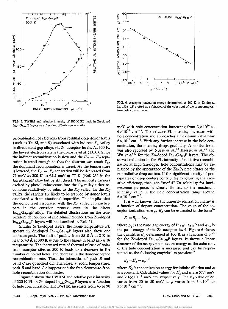
FIG. 5. FWJXM and relative intensity of 300-K PL peak in %-doped Ine32Gae,a8P layers as a function of hole concentration.
recombination of electrons from residual deep donor levels (such as Te, Si, and S) associated with indirect Xc valley in direct band gap alloys via Zn acceptor levels. At 300 K, the lowest electron state is the donor level at ( l,O,O). Since the indirect recombination is slow and the EC - ED sepa- ration is small enough so that the electron can reach l?c, the dominant recombination is direct. As the temperature is lowered, the PC - Xc separation will be decreased from 79 meV at 300 K to 65.5 meV at 77 K (Ref. 23) in the Ino.3zGae68P alloy but be still direct. The minority carriers excited by photoluminescence into the Ic valley either re- combine radiatively or relax to the Xc valley. In the Xc valley, the carriers are likely to be trapped by donor levels associated with unintentional impurities. This implies that the donor level associated with the Xc valley can partici- pate in the emission process even in the direct Ino.32Gae68P alloy. The detailed illustrations on the tem- perature dependence of photoluminescence from Zn-doped Ine32Gae.6sP layers will be described in Ref. 24.
Similar to Te-doped layers, the room-temperature PL spectra in Zn-doped Ine32Gae&sP layers also show one emission peak. The shift of peak A from 5510 A at 8 K to near 5740 A at 300 K is due to the change in band gap with temperature. The increased rate of thermal release of holes from acceptor sites at 300 K leads to a decrease in the number of bound holes, and decrease in the donor-acceptor recombination rate. Thus the intensities of peak B and band C are quenched off. Therefore, at room temperature, peak B and band C disappear and the free-electron-to-free- hole recombination dominates.
Figure 5 shows the FWHM and relative peak intensity of 300 K PL in Zn-doped Ine32Gac&jP layers as a function of hole concentration. The FWHM increases from 43 to 90
5043 J. Appl. Phys., Vol. 70, No. 9, 1 November 1991
I I I I I
2x10⁻³ 4 5 6 7 6 c
9 1x10’ 2 3X10⁶
l/3 P ( cm-’ 1
FIG. 6. Acceptor ionization energy determined at 100 K in Zn-doped IQ~G~,,~~P plotted as a function of the cube root of the room-tempera- ture hole concentration.
meV with hole concentration increasing from 3 X 10¹⁶ to 6x 1018 cm - 3. The relative PL intensity increases with hole concentration and approaches a maximum value near 6 x lOI7 cm - 3. With any further increase in the hole con- centration, the intensity drops gradually. A similar trend was also reported by Nuese et a1.,18 Kressel et a1.,25 and Wu et a1.17 for the Zn-doped Ino.sGao.sP layers. The ob- served reduction in the PL intensity of radiative recombi- nation at high Zn-doped hole concentrations may be ex- plained by the appearance of the Zn3P2 precipitates or the nonradiative deep centers. If the significant density of pre- cipitates or deep centers contributes to lowering the radi- ative efficiency, then, the ‘?.tseful” Zn solubility for lumi- nescence purposes is clearly limited to the maximum intensity value in the hole concentration range around 6~10'~ cmv3.
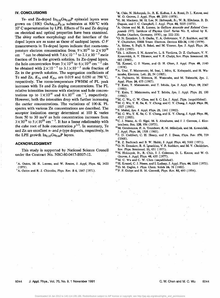
It is well known that the impurity ionization energy is a function of dopant concentration. The value of the ac- ceptor ionization energy EA can be estimated in the form26
E.4 = Eg - hvB,
where Eg is the band gap energy of Ino.32Gae68P and hvB is the peak energy of the Zn acceptor level. Figure 6 shows the quantities EA determined at 100 K as a function ofp1’3 for the Zn-doped Ine~2Gac&sP layers. It shows a linear decrease of the acceptor ionization energy as the cube root of the hole concentration is increased and can be rerpre- sented as the following empirical expression:27
EA =,$ - c~p~‘~,
where I$ is the ionization energy for infinite dilution and a is a constant. Calculated values for @d and a are 57.4 meV and 2.4~ 10 - 5 meV cm, respectively. The EA value of Zn varies from 50 to 30 meV as p varies from 3 X 10¹⁶ to 5x10¹⁸ cme3.
C. W. Chen and M. C. Wu 5043
Downloaded 16 Jan 2012 to 140.114.195.186. Redistribution subject to AIP license or copyright; see http://jap.aip.org/about/rights_and_permissions
IV. CONCLUSlONS
Te- and Zn-doped Ino.s2Gaa6sP epitaxial layers were grown on (100) GaA~,,~iPe.s~ substrates at 800 “C with lo” C supersaturation by LPE. Effects of Te and Zn doping on electrical and optical properties have been examined. The shiny surface morphology and flat interface of the doped layers are as same as those of undoped layers. C-V measurements in Te-doped layers indicate that room-tem- perature electron concentration from 9X lOI to 2X lo’* cm - 3 can be obtained with 7.6 x 10 - 3 to 2.1 X 10 - 3 mole fraction of Te in the growth solution. In Zn-doped layers, the hole concentration from 3 X 10¹⁶ to 6X lo’* cm -’ can be obtained with 2 x 10 - 5 to 3.1 X 10 - 3 mole fraction of Zn in the growth solution. The segregation coefficients of Te and Zn, KTe and KZn, are 0.019 and 0.050 at 798 “C, respectively. The room-temperature FWHM of PL peak increases with Te and Zn doping concentrations. The PL relative intensities increase with electron and hole concen- trations up to 1 X 10r8 and 6X 1017 cm- 3, respectively. However, both the intensities drop with further increasing the carrier concentrations. The variations of 100-K PL spectra with various Zn concentrations are described. The acceptor ionization energy determined at 100 K varies from 50 to 30 meV as hole concentration increases from 3 x lOI to 5 X 10” cm- 3. It has a linear relationship with the cube root of hole concentration P”~. In summary, Te and Zn are excellent n- and p-type dopants, respectively, in the LPE grodvth 1~.3&&&? layers.
ACKNOWLEDGMENT
This study is supported by National Science Council under the Contract No. NSC-80-0417~EOO7-12.
‘A. Gnton, M. R. Lorenz, and W. Reuter, J. Appl.. Phys. 42, 3420 (1971).
‘A. Onton and R. J. Chicotka, Phys. Rev. B 4, 1847 (1971).
“R. Chin, N. Holonyak, Jr., R. K. Kolbas, J. A. Rossi, D. L. Keune, and W. 0. Groves, J. Appl. Phys. 49, 2551 (1978).
“H. M. Macksey, M. H. Lee, N. Holonyak, Jr., W. R. Hitchens, R. D. Dupuis, and J. C. Campbell, J. Appl. Phys. 44, 5035 (1973).
‘A. Onton and M. R. Lorenz, in Gallium Arsenide and Related Com- pounds 1971, Institute of Physics Conf. Series No. 9, edited by K. Paulus (Aachen, Germany, 1970), pp. 222-230.
60. N. Ermakov, L. S. Garba, Y. A. Golovanov, V. P. Sushkov, and M. V. Chukichev, IEEE Trans. Electron. Devices’ ED-26, 1190 (1979).
‘A. Shima, S. Fujii, S. Sakai, and M. Umeno; Jpn. J. Appl. Phys. 24, L233 (1985).
*Zh. I. Alferov, I. N. Arsent’ev, L. S. Vavilova, D. Z. Garbuzov, V. V. Krasovskii, A. V. Tikunov, and V. P. Chalyi, Sov. Phys. Semicond. 19, 683 (1985).
‘H. Kressel, C. J. Nuese, and G. H. Olsen, J. Appl. Phys. 49, 3140 (1978).
“A. Usui, T. Matsumoto, M. Inai, I. Mito, K. Kobayashi, and H. Wa- tanabe, Electron. Lett. 21, 54 (1985).
“A. Fujimoto, M. Shimura, H. Watanabe, and M. Takeuchi, Jpn. J. Appl. Phys. 26, 675 (1987).
“T. Kato, T. Matsumoto, and T. Ishida, Jpn. J. Appl. Phys. 19, 2367 (1980).
“T. Kato, T. Matsumoto, and T. Ishida, Jpn. J. Appl. Phys. 21, 100 (1982).
14M. C. Wu, C. W. Chen, and S. C. Lu, J. Appl. Phys. (unpublished). isM. C. Wu, Y. K. Su, K. Y. Cheng, and C. Y. Chang, J. Appl. Phys. 58,
1537 (1985). ‘%. Mukai, Jpn. J. Appl. Phys. 21, 1141 (1982). I’M. C. Wu, Y. K. Su, C Y. Chang, and K. Y. Cheng, J. Appl. Phys. 58,
4317 (1985). ‘*C. J. Nuese, A. G. Sigai, M. S. Abrahams, and J. J. Gannon, J. Elec-
trochem. Sot. 120, 956 (1973). 19M. Gershenzon, F. A. Trumbore, R. M. Mikulyak, and M. Kowalchik,
J. Appl. Phys. 36, 1528 ( 1965). ‘aJ. D. Cuthbert, C. H. Henry, and P. J. Dean, Phys. Rev. 170, 739
(1968). ‘lR. Z. Bachrach and B. W. Hakki, J. Appl. Phys. 42, 5102 ( 1971). z’0. N. Ermakov, R. S. Ignatkina, V. P. Sushkov, and M. V. Chukichev,
Sov. Phys. Semicond. 11, 651 (1977). “N. Holonyak, Jr., R. Chin, J. J. Coleman, D. L. Keune, and W. 0.
Groves, J. Appl. Phys. 48, 635 (1977). %MM. C. Wu and C. W. Chen (unpublished). *‘H. Kressel, C. J. Nuese, and I. Ladany, J. Appl. Phys. 44, 3266 (1973). 26D; M. Eagles, J. Phys. Chem. Solids 16, 76 (1960). “P. P. Debye and E. M. Conwell, Phys. Rev. 93, 693 (1954).
5044 J. Appl. Phys., Vol. 70, No. 9, 1 November 1991 G. W. Chen and M. C. Wu 5044
Downloaded 16 Jan 2012 to 140.114.195.186. Redistribution subject to AIP license or copyright; see http://jap.aip.org/about/rights_and_permissions