1
Epoxy T echnology Inc. • 14 Fortune Drive • Billerica, MA 01821 phone 978-667-3805 fax 978-663-9782 T oll Free 800-227-2201 [email protected] © Epoxy Technology Inc. 2013 epotek.com is paper summarizes the technical requirements of enabling polyimide layers above semiconductor wafers, through the use of screen print deposition. In order for this process to be realized, the paper compares and contrasts screen printing to the “historical spin- on method of spin-on process” and illustrates the latter’s inherent disadvantages. e paper also provides useful product test data for the polyimide itself, along with supporting analytical curves and data. Tech Paper #041 Conclusions Summary Screen printing polyimides is a two-step process, compared to “historical spin-on methods” requiring 7+ steps. Screen printing is a cost savings over the spin-on process by significantly reducing the amount of waste per wafer. EPO-TEK® 600, a polyimide used in the wafer coating process, is an excellent choice for this application. (EPO-TEK® 600 has been replaced by EPO-TEK® TV1002 and TV1003.) Suggested screen printing parameters are provided for initial set-up. Potential applications include: mechanical buffering for reducing scrap rate in the back-lapping process and acting as an alpha particle barrier in memory chips. Applications of patterned polyimide adhesive on the active side of wafers can be used in 3D chip packaging formats, as well as dielectric and thermally dissipative coating on high power wafers. Wafer Protection with Screen Printable Polyimide By Frank W. Kulesza & Richard H. Estes Epoxy Technology EPO-300-01 TECHNICAL OVERVIEW epotek.com

epotek.com TECHNICAL OVERVIEW This paper summarizes the technical ... on method of spin-on process” and illustrates the latter’s inherent disadvantages ... • Suggested screen

Embed Size (px)

Citation preview

Epoxy Technology Inc. • 14 Fortune Drive • Billerica, MA 01821phone 978-667-3805 fax 978-663-9782 Toll Free 800-227-2201 [email protected]© Epoxy Technology Inc. 2013

epotek.com

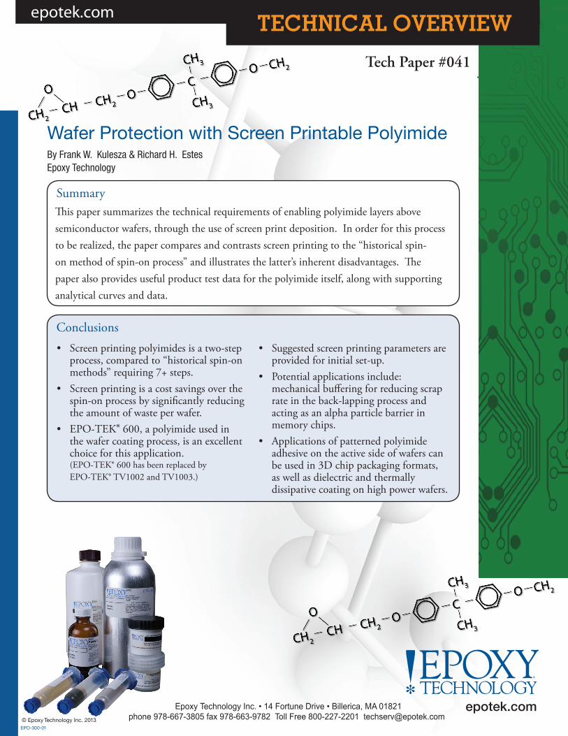
This paper summarizes the technical requirements of enabling polyimide layers above semiconductor wafers, through the use of screen print deposition. In order for this process to be realized, the paper compares and contrasts screen printing to the “historical spin-on method of spin-on process” and illustrates the latter’s inherent disadvantages. The paper also provides useful product test data for the polyimide itself, along with supporting analytical curves and data.

Tech Paper #041

Conclusions

Summary

• Screen printing polyimides is a two-step process, compared to “historical spin-on methods” requiring 7+ steps.

• Screen printing is a cost savings over the spin-on process by significantly reducing the amount of waste per wafer.

• EPO-TEK® 600, a polyimide used in the wafer coating process, is an excellent choice for this application. (EPO-TEK® 600 has been replaced by EPO-TEK® TV1002 and TV1003.)

• Suggested screen printing parameters are provided for initial set-up.

• Potential applications include: mechanical buffering for reducing scrap rate in the back-lapping process and acting as an alpha particle barrier in memory chips.

• Applications of patterned polyimide adhesive on the active side of wafers can be used in 3D chip packaging formats, as well as dielectric and thermally dissipative coating on high power wafers.

Wafer Protection with Screen Printable PolyimideBy Frank W. Kulesza & Richard H. Estes Epoxy Technology

EPO-300-01

TECHNICAL OVERVIEWepotek.com