Embed Size (px)
Citation preview
TECH. CORP.
SPECIFICATIONS
CUSTOMER : SAMPLE CODE : SH240320T-062-L-Q MASS PRODUCTION CODE : PH240320T-062-L-Q SAMPLE VERSION : 02 SPECIFICATIONS EDITION : 007 DRAWING NO. (Ver.) : LMD-PH240320T-062-L-Q (Ver.003) PACKAGING NO. (Ver.) : PKG-PH240320T-062-L-Q (Ver:001)
Customer Approved
Date:
Approved Checked Designer
閆偉 張久慧 劉進
□ Preliminary specification for design input ■ Specification for sample approval
POWERTIP TECH. CORP. Headquarters:
No.8, 6th Road, Taichung Industrial Park,
Taichung, Taiwan
台中市 407工業區六路 8號
TEL: 886-4-2355-8168
FAX: 886-4-2355-8166
E-mail: [email protected]
Http://www.powertip.com.tw
NO.PT-A-005-8
PH240320T-062-L-Q Page2 SAMPLE Ver.02
SPEC Edi.007
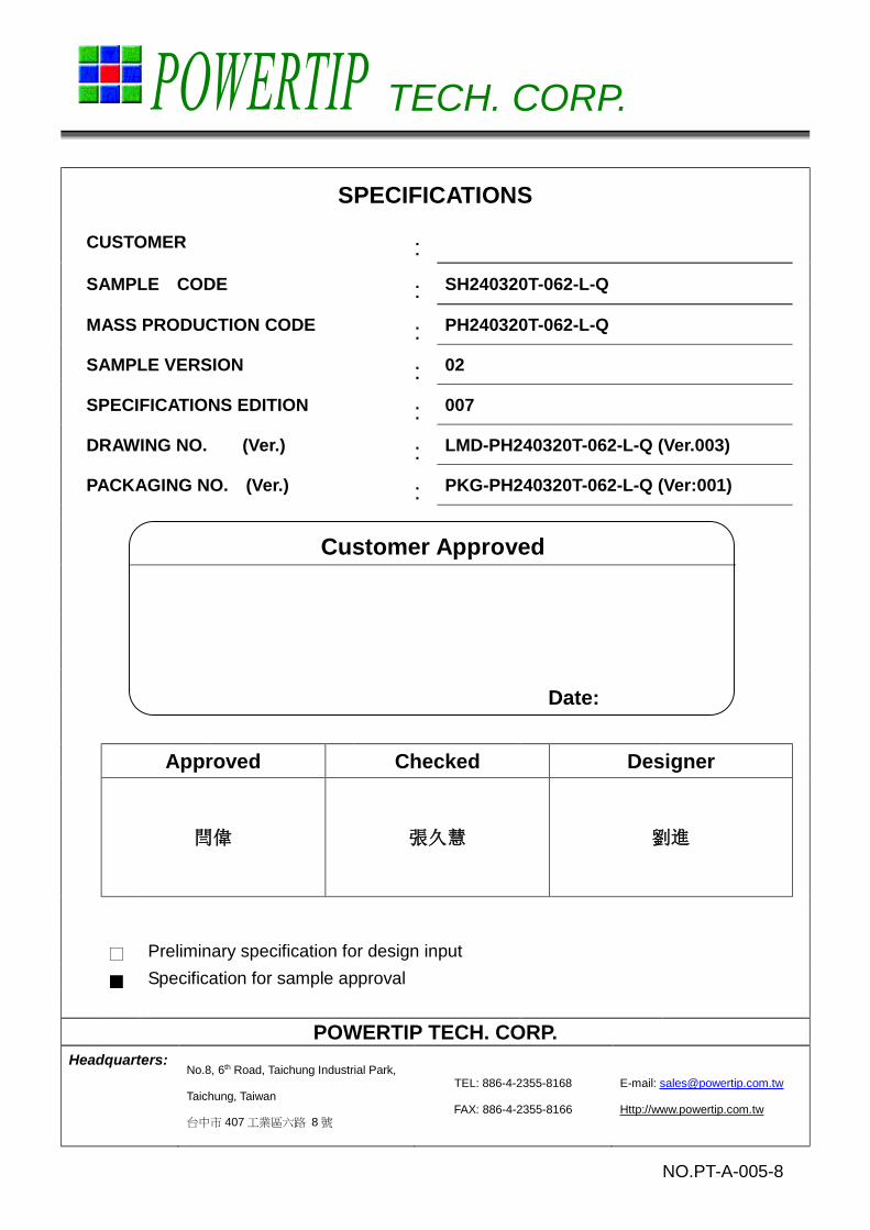
History of Version Date
(mm / dd / yyyy) Ver. Edi. Description Page Design by
08/03/2012 01 001 New Drawing - Howard
08/20/2012 01 002 Modify TFT Size Appendix Howard
09/14/2012 01 003 New Sample
Modify Interface Pin Description -
11,12 Howard
12/12/2012 02 004 Second Sample
Modify Optical Characteristics Modify Drawing
- 6
Appendix Howard
03/24/2014 02 005 Modify Contrast Ratio 6 Howard
08/24/2014 02 006 Show Backlight Life Time 9 劉進
08/27/2015 02 007 Modify Backlight Life Time 9 劉進
Total: 32 Page
PH240320T-062-L-Q Page3 SAMPLE Ver.02
SPEC Edi.007
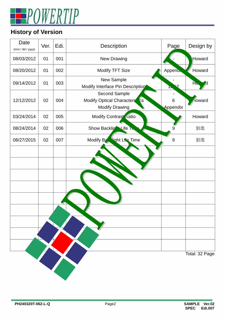
Contents 1. SPECIFICATIONS 1.1 Features 1.2 Mechanical Specifications 1.3 Absolute Maximum Ratings 1.4 DC Electrical Characteristics 1.5 Optical Characteristics 1.6 Backlight & LED Characteristics 2. MODULE STRUCTURE 2.1 Counter Drawing 2.2 Interface Pin Description 2.2.1 Application Notes 2.2.2 Refer Initial code 2.3 Timing Characteristics
3. QUALITY ASSURANCE SYSTEM 3.1 Quality Assurance Flow Chart 3.2 Inspection Specification
4. RELIABILITY TEST 4.1 Reliability Test Condition
5. PRECAUTION RELATING PRODUCT HANDLING 5.1 Safety 5.2 Handling 5.3 Storage 5.4 Terms of Warranty
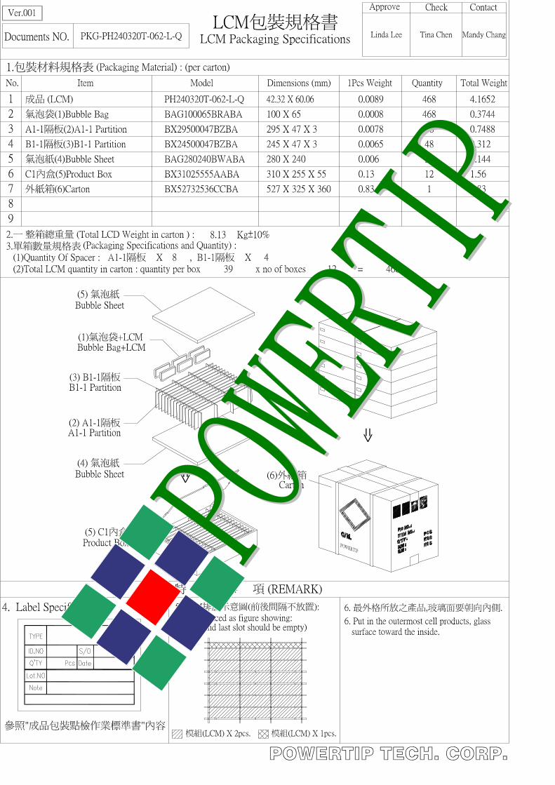
Appendix:LCM Drawing
Packaging Note:For detailed information please refer to IC data sheet:ILITEK – ILI9341
PH240320T-062-L-Q Page4 SAMPLE Ver.02
SPEC Edi.007
1. SPECIFICATIONS
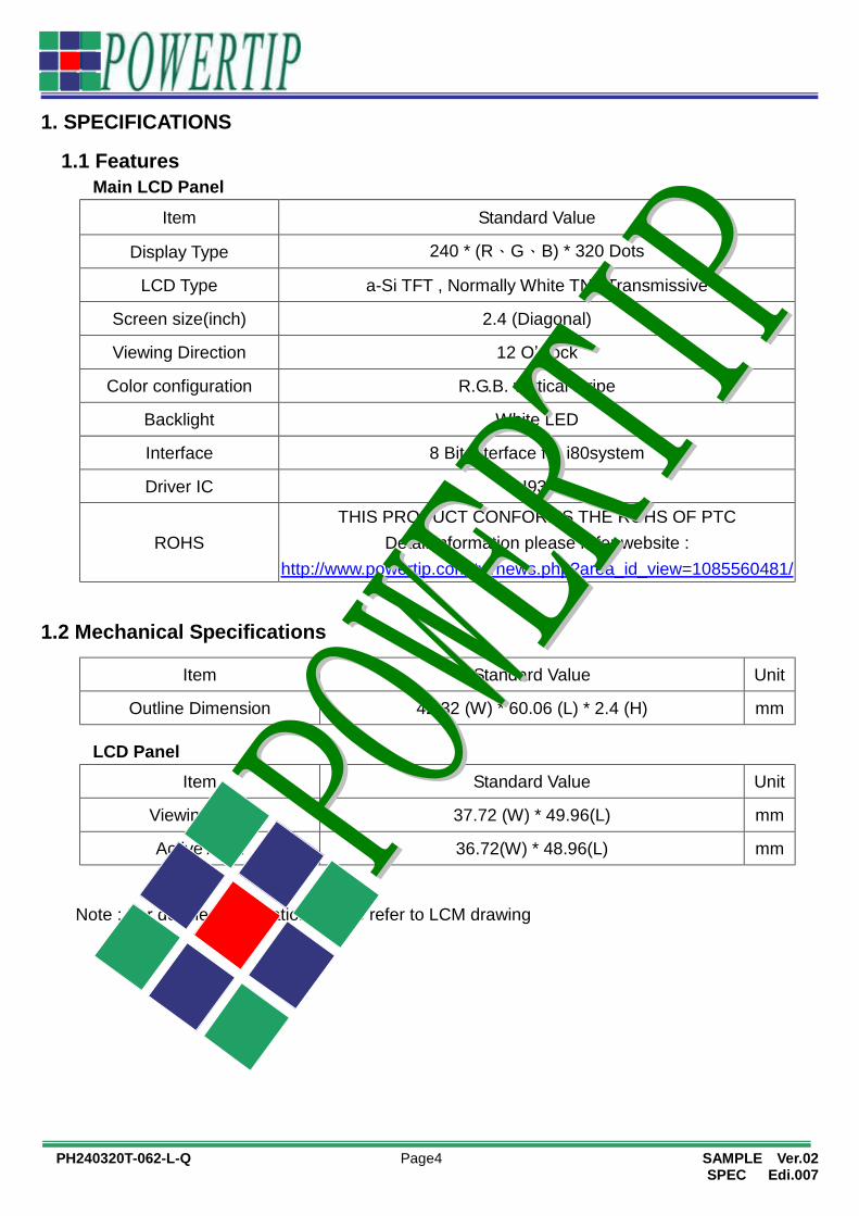
1.1 Features Main LCD Panel
Item Standard Value
Display Type 240 * (R、G、B) * 320 Dots
LCD Type a-Si TFT , Normally White TN , Transmissive
Screen size(inch) 2.4 (Diagonal)
Viewing Direction 12 O’clock
Color configuration R.G.B. vertical stripe
Backlight White LED
Interface 8 Bit Interface for i80system
Driver IC ILI9341
ROHS THIS PRODUCT CONFORMS THE ROHS OF PTC
Detail information please refer website : http://www.powertip.com.tw/news.php?area_id_view=1085560481/
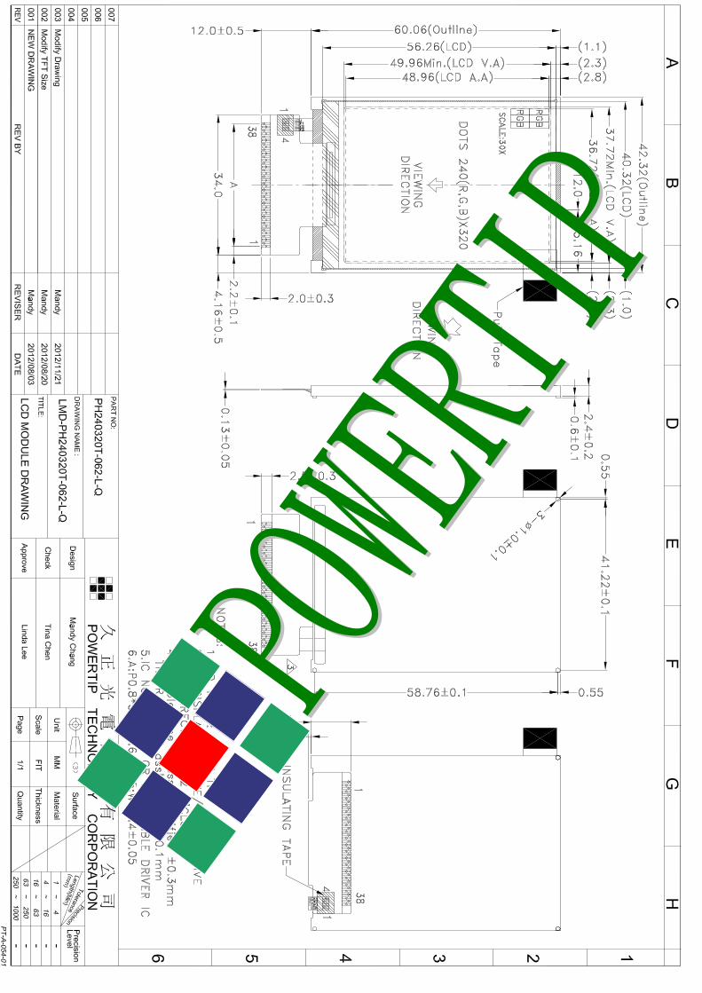
1.2 Mechanical Specifications
Item Standard Value Unit
Outline Dimension 42.32 (W) * 60.06 (L) * 2.4 (H) mm
LCD Panel Item Standard Value Unit
Viewing Area 37.72 (W) * 49.96(L) mm
Active Area 36.72(W) * 48.96(L) mm
Note : For detailed information please refer to LCM drawing
PH240320T-062-L-Q Page5 SAMPLE Ver.02
SPEC Edi.007
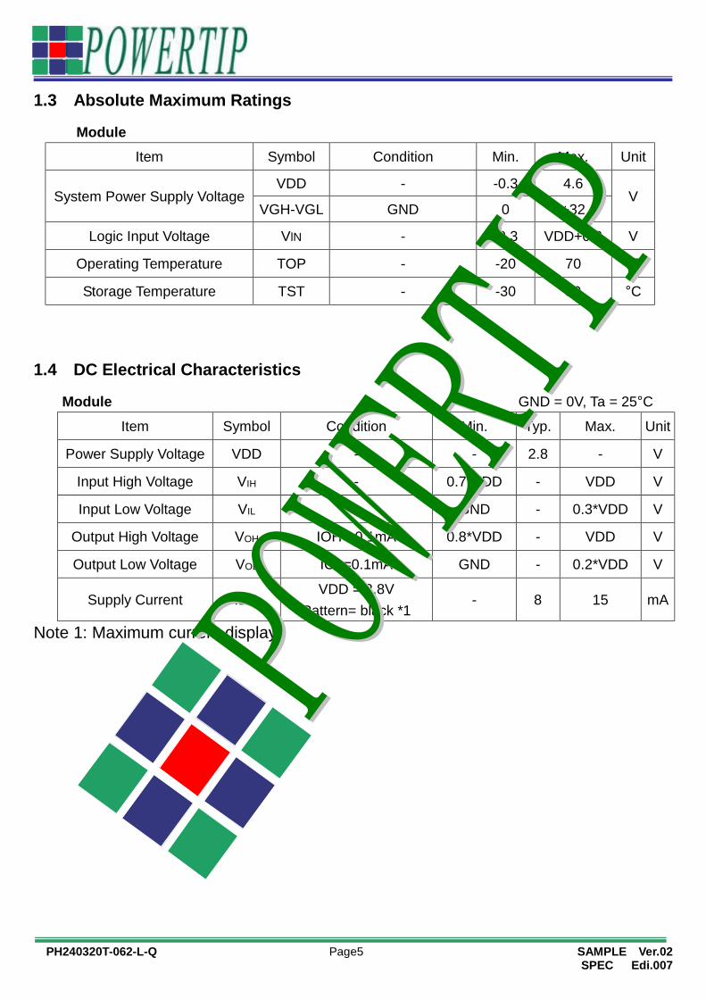
1.3 Absolute Maximum Ratings
Module Item Symbol Condition Min. Max. Unit
System Power Supply Voltage VDD - -0.3 4.6
V VGH-VGL GND 0 +32
Logic Input Voltage VlN - -0.3 VDD+0.3 V
Operating Temperature TOP - -20 70 °C
Storage Temperature TST - -30 80 °C
1.4 DC Electrical Characteristics
Module GND = 0V, Ta = 25°C Item Symbol Condition Min. Typ. Max. Unit
Power Supply Voltage VDD - - 2.8 - V
Input High Voltage VIH - 0.7*VDD - VDD V
Input Low Voltage VIL - GND - 0.3*VDD V
Output High Voltage VOH IOH=-0.1mA 0.8*VDD - VDD V
Output Low Voltage VOL IOL=0.1mA GND - 0.2*VDD V
Supply Current IDD VDD = 2.8V
Pattern= black *1 - 8 15 mA
Note 1: Maximum current display
PH240320T-062-L-Q Page6 SAMPLE Ver.02
SPEC Edi.007
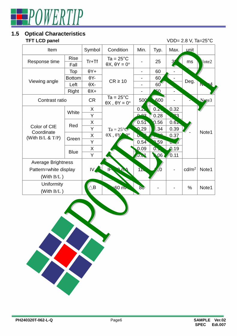
1.5 Optical Characteristics TFT LCD panel VDD= 2.8 V, Ta=25°C
Item Symbol Condition Min. Typ. Max. unit
Response time Rise
Tr+Tf Ta = 25°C θX, θY = 0° - 25 38 ms Note2
Fall
Viewing angle
Top θY+
CR ≥ 10
- 60 -
Deg.
Note4 Bottom θY- - 60 -
Left θX- - 60 - Right θX+ - 60 -
Contrast ratio CR Ta = 25°C θX , θY = 0° 500 600 - - Note3
Color of CIE Coordinate
(With B/L & T/P)
White X
Ta = 25°C θX , θY = 0°
0.22 0.27 0.32
- Note1
Y 0.23 0.28 0.33
Red X 0.51 0.56 0.61 Y 0.29 0.34 0.39
Green X 0.27 0.32 0.37 Y 0.54 0.59 0.64
Blue X 0.09 0.14 0.19 Y 0.01 0.06 0.11
Average Brightness Pattern=white display
(With B/L ) IV IF=60 mA 110 120 - cd/m2 Note1
Uniformity (With B/L )
△B IF=60 mA 80 - - % Note1
PH240320T-062-L-Q Page7 SAMPLE Ver.02
SPEC Edi.007
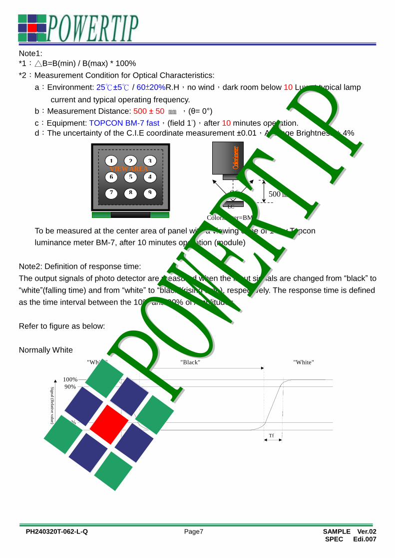
Note1: *1:△B=B(min) / B(max) * 100% *2:Measurement Condition for Optical Characteristics:
a:Environment: 25 ±℃ 5℃ / 60±20%R.H,no wind,dark room below 10 Lux at typical lamp current and typical operating frequency.
b:Measurement Distance: 500 ± 50 ㎜ ,(θ= 0°) c:Equipment: TOPCON BM-7 fast,(field 1°),after 10 minutes operation.
d:The uncertainty of the C.I.E coordinate measurement ±0.01,Average Brightness ± 4%
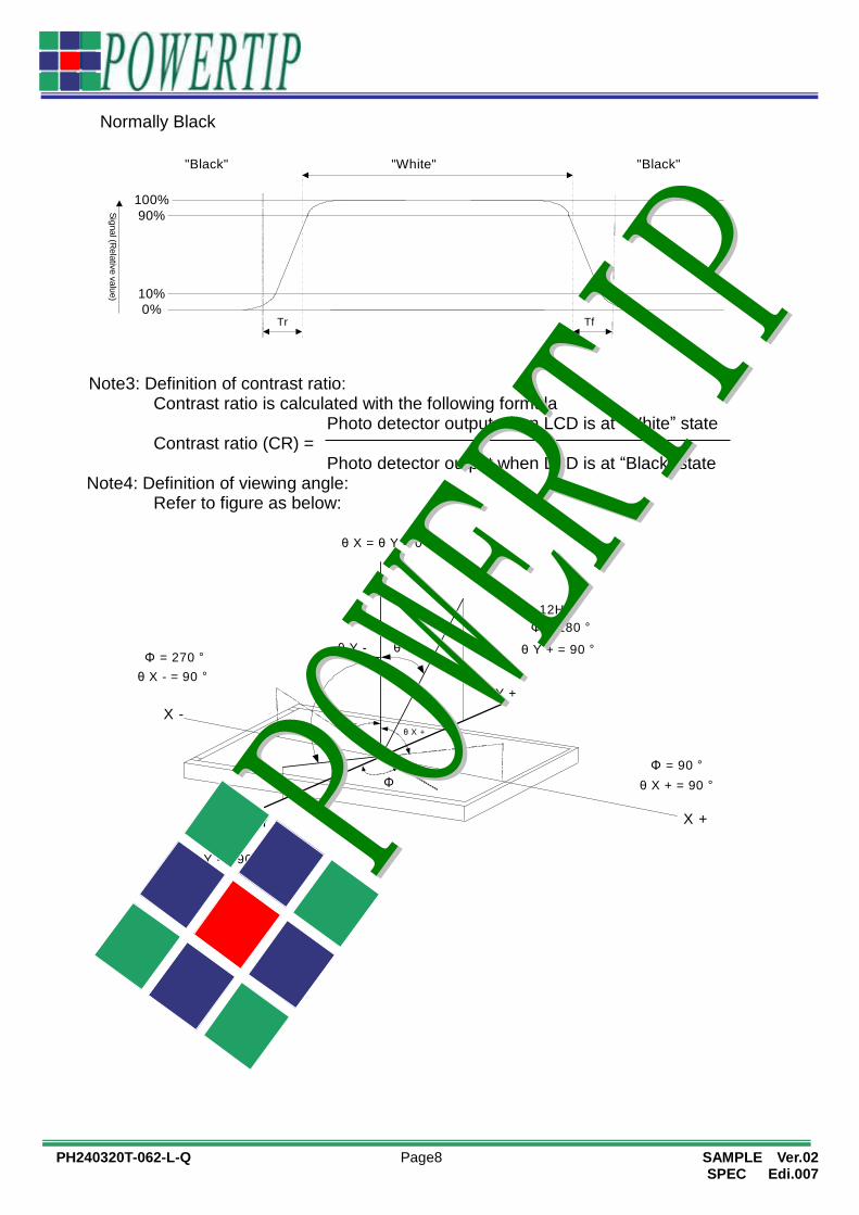
To be measured at the center area of panel with a viewing cone of 1° by Topcon luminance meter BM-7, after 10 minutes operation (module) Note2: Definition of response time: The output signals of photo detector are measured when the input signals are changed from “black” to “white”(falling time) and from “white” to “black”(rising time), respectively. The response time is defined as the time interval between the 10% and 90% of Amplitudes. Refer to figure as below: Normally White
1 2 3
6 5 4
7 8 9
VIEW AREA
LC
θ θ
Colorimeter=BM-7
500㎜
100%90%
10%0%
Signal (Relative value)
"Black"
Tr Tf
"White" "White"
PH240320T-062-L-Q Page8 SAMPLE Ver.02
SPEC Edi.007
Normally Black
Note3: Definition of contrast ratio: Contrast ratio is calculated with the following formula Photo detector output when LCD is at “White” state Contrast ratio (CR) = Photo detector output when LCD is at “Black” state
Note4: Definition of viewing angle: Refer to figure as below:
θ X - = 90 °
θ Y - = 90 °
X -
Y -
θ Y + = 90 °
θ X + = 90 °
X +
θ Y - θ Y +
θ X -θ X +
Y +
θ X = θ Y = 0°
Φ
Φ = 0 °6 H
Φ = 270 °
Φ = 90 °
Φ = 180 °12H
100%90%
10%0%
Signal (R
elative value)
"Black"
Tr Tf
"White""Black"
PH240320T-062-L-Q Page9 SAMPLE Ver.02
SPEC Edi.007
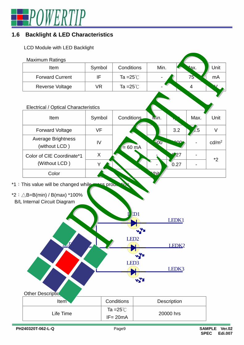
1.6 Backlight & LED Characteristics
LCD Module with LED Backlight
Maximum Ratings Item Symbol Conditions Min. Max. Unit
Forward Current IF Ta =25℃ - 75 mA
Reverse Voltage VR Ta =25℃ - 4 V
Electrical / Optical Characteristics
Item Symbol Conditions Min. Typ. Max. Unit
Forward Voltage VF
IF= 60 mA
- 3.2 3.5 V
Average Brightness (without LCD )
IV 2500 2800 - cd/m2
Color of CIE Coordinate*1 (Without LCD )
X - 0.27 - *2
Y - 0.27 -
Color White
*1:This value will be changed while mass production.
*2:△B=B(min) / B(max) *100% B/L Internal Circuit Diagram
LED2
LED1
LED3
LEDA
LEDK1
LEDK2
LEDK3
Other Description
Item Conditions Description
Life Time Ta =25℃ IF= 20mA
20000 hrs
PH240320T-062-L-Q Page10 SAMPLE Ver.02
SPEC Edi.007
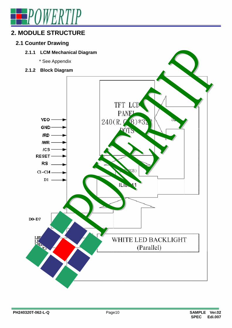
2. MODULE STRUCTURE 2.1 Counter Drawing
2.1.1 LCM Mechanical Diagram
* See Appendix
2.1.2 Block Diagram
PH240320T-062-L-Q Page11 SAMPLE Ver.02
SPEC Edi.007
2.2 Interface Pin Description
Pin No. Symbol Function
1 GND System Ground.(0V)
2 RESET This signal will reset the device and must be applied to properly initialize the chip. Signal is active low.
3 DB7 Bi-directional data bus.
4 DB6 Bi-directional data bus.
5 DB5 Bi-directional data bus.
6 DB4 Bi-directional data bus.
7 DB3 Bi-directional data bus.
8 DB2 Bi-directional data bus.
9 DB1 Bi-directional data bus.
10 DB0 Bi-directional data bus.
11 RD Serves as a read signal and MCU read data at the rising edge.
12 /WR Serves as a write signal and writes data at the rising edge.
13 RS When RS = ’1’, data is selected. When RS = ’0’, command is selected.
14 /CS Chip select input pin (“Low” enable).
15 VDD_C1 Not Connect.
16 VCOMH_C2 Not Connect.
17 VCOML_C3 Not Connect.
18 GVDD_C4 Not Connect.
19 VCL_C5 VCL pad. Place a 1uF/10V capacitor to GND.
20 AVDD_C6 AVDD pad. Place a 1uF/10V capacitor to GND.
21 VCI1_C7 VCI1 pad. Place a 1uF/10V capacitor to GND.
22 C12N Place a 1uF/10V capacitor between C12N and C12P.
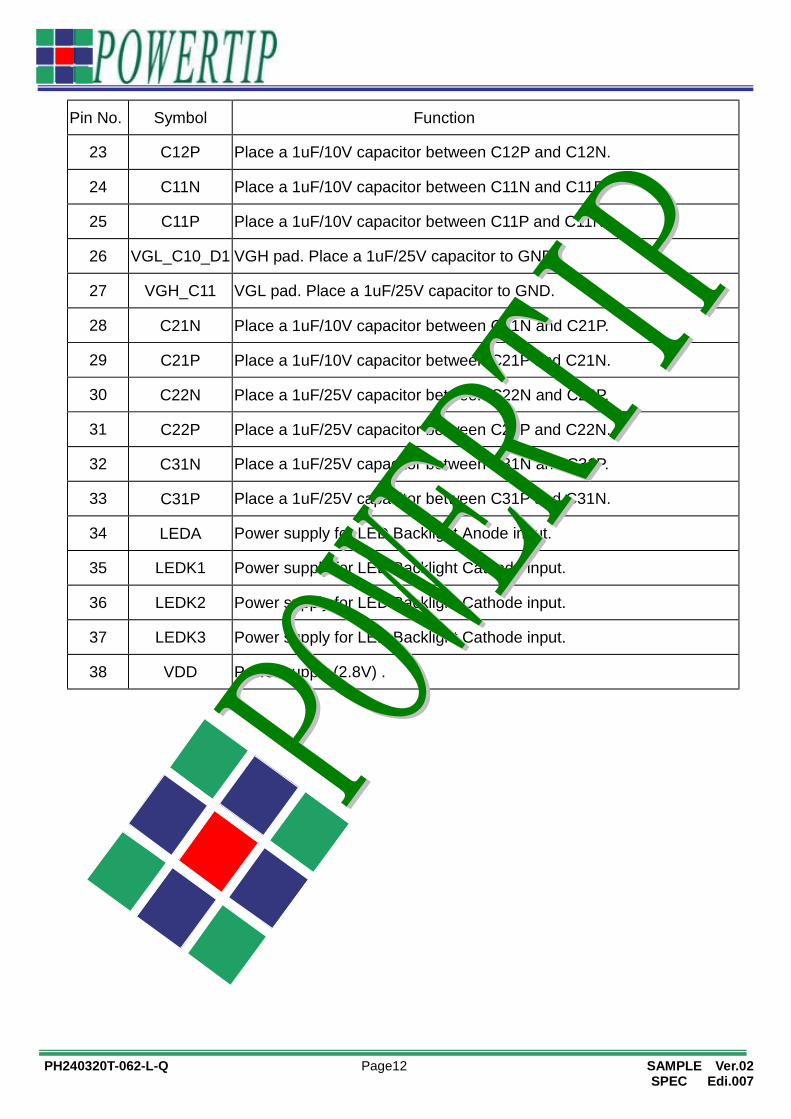
PH240320T-062-L-Q Page12 SAMPLE Ver.02
SPEC Edi.007
Pin No. Symbol Function
23 C12P Place a 1uF/10V capacitor between C12P and C12N.
24 C11N Place a 1uF/10V capacitor between C11N and C11P.
25 C11P Place a 1uF/10V capacitor between C11P and C11N.
26 VGL_C10_D1 VGH pad. Place a 1uF/25V capacitor to GND.
27 VGH_C11 VGL pad. Place a 1uF/25V capacitor to GND.
28 C21N Place a 1uF/10V capacitor between C21N and C21P.
29 C21P Place a 1uF/10V capacitor between C21P and C21N.
30 C22N Place a 1uF/25V capacitor between C22N and C22P.
31 C22P Place a 1uF/25V capacitor between C22P and C22N.
32 C31N Place a 1uF/25V capacitor between C31N and C31P.
33 C31P Place a 1uF/25V capacitor between C31P and C31N.
34 LEDA Power supply for LED Backlight Anode input.
35 LEDK1 Power supply for LED Backlight Cathode input.
36 LEDK2 Power supply for LED Backlight Cathode input.
37 LEDK3 Power supply for LED Backlight Cathode input.
38 VDD Power supply.(2.8V) .
PH240320T-062-L-Q Page13 SAMPLE Ver.02
SPEC Edi.007
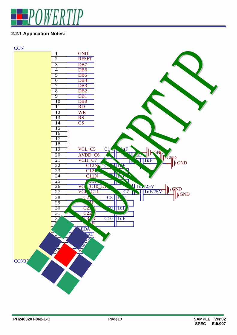
2.2.1 Application Notes:
1234567891011121314151617181920212223242526272829303132333435363738
CON
CON37
GNDRESETDB7DB6DB5DB4DB3DB2DB1DB0RDWRRSCS
VCL_C5AVDD_C6VCI1_C7
C12NC12PC11NC11P
VGL_C10_D1VGH_C11
C21NC21PC22NC22P
VDD
LEDALEDK1LEDK2LEDK3
C31NC31P
GNDC1 1uF
C2 1uF GNDC3 1uF GNDC4 1uF
C5 1uF
C6 1uF/25V GNDC7 1uF/25V GNDC8 1uF
C9 1uF
C10 1uF
PH240320T-062-L-Q Page14 SAMPLE Ver.02
SPEC Edi.007
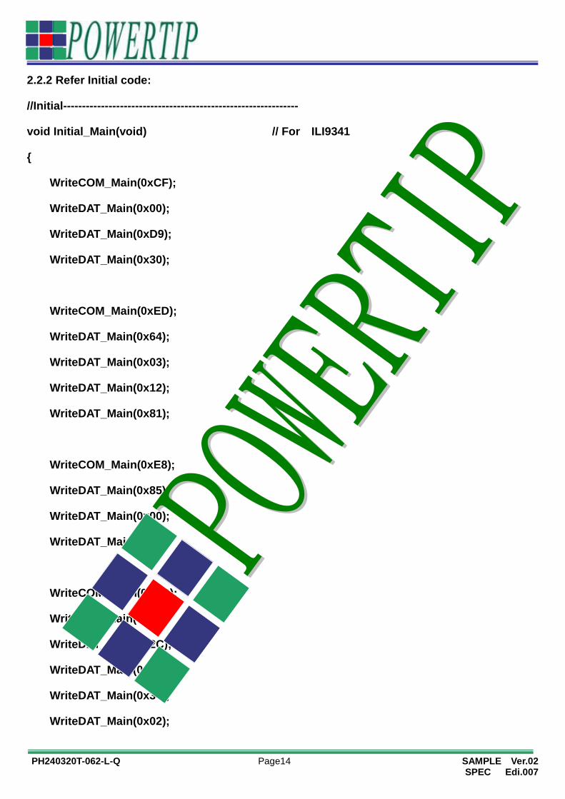
2.2.2 Refer Initial code:
//Initial--------------------------------------------------------------
void Initial_Main(void) // For ILI9341
{
WriteCOM_Main(0xCF);
WriteDAT_Main(0x00);
WriteDAT_Main(0xD9);
WriteDAT_Main(0x30);
WriteCOM_Main(0xED);
WriteDAT_Main(0x64);
WriteDAT_Main(0x03);
WriteDAT_Main(0x12);
WriteDAT_Main(0x81);
WriteCOM_Main(0xE8);
WriteDAT_Main(0x85);
WriteDAT_Main(0x00);
WriteDAT_Main(0x78);
WriteCOM_Main(0xCB);
WriteDAT_Main(0x39);
WriteDAT_Main(0x2C);
WriteDAT_Main(0x00);
WriteDAT_Main(0x34);
WriteDAT_Main(0x02);
PH240320T-062-L-Q Page15 SAMPLE Ver.02
SPEC Edi.007
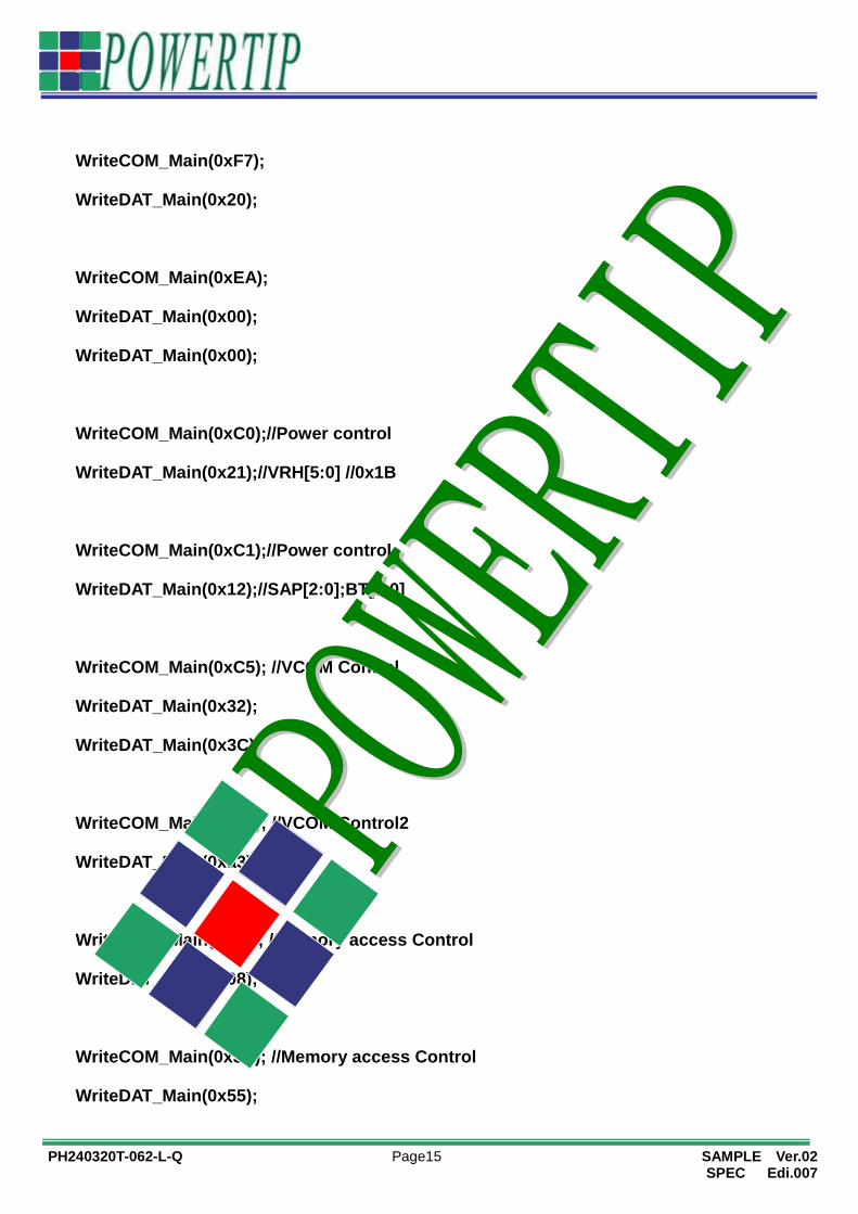
WriteCOM_Main(0xF7);
WriteDAT_Main(0x20);
WriteCOM_Main(0xEA);
WriteDAT_Main(0x00);
WriteDAT_Main(0x00);
WriteCOM_Main(0xC0);//Power control
WriteDAT_Main(0x21);//VRH[5:0] //0x1B
WriteCOM_Main(0xC1);//Power control
WriteDAT_Main(0x12);//SAP[2:0];BT[3:0]
WriteCOM_Main(0xC5); //VCOM Control
WriteDAT_Main(0x32);
WriteDAT_Main(0x3C);
WriteCOM_Main(0xC7); //VCOM Control2
WriteDAT_Main(0xa3); //0x9D
WriteCOM_Main(0x36); //Memory access Control
WriteDAT_Main(0x08);
WriteCOM_Main(0x3A); //Memory access Control
WriteDAT_Main(0x55);
PH240320T-062-L-Q Page16 SAMPLE Ver.02
SPEC Edi.007
WriteCOM_Main(0xB1);
WriteDAT_Main(0x00);
WriteDAT_Main(0x1B);
WriteCOM_Main(0xB6); //Display Function
WriteDAT_Main(0x0a);
WriteDAT_Main(0xa2);
WriteCOM_Main(0xF6);
WriteDAT_Main(0x01);
WriteDAT_Main(0x30);
WriteCOM_Main(0xF2); //3Gamma Function Disable
WriteDAT_Main(0x00);
WriteCOM_Main(0x26); //Gamma Curve select
WriteDAT_Main(0x01);
//-----------set gamma-----------------

PH240320T-062-L-Q Page17 SAMPLE Ver.02
SPEC Edi.007
WriteCOM_Main(0xe0); //set gamma
WriteDAT_Main(0x0f);
WriteDAT_Main(0x1c);
WriteDAT_Main(0x19);
WriteDAT_Main(0x08);
WriteDAT_Main(0x0b);
WriteDAT_Main(0x04);
WriteDAT_Main(0x4b);
WriteDAT_Main(0x64);
WriteDAT_Main(0x3e);
WriteDAT_Main(0x09);
WriteDAT_Main(0x15);
WriteDAT_Main(0x08);
WriteDAT_Main(0x16);
WriteDAT_Main(0x0D);
WriteDAT_Main(0x04);
WriteCOM_Main(0xe1); //set gamma
WriteDAT_Main(0x00);
WriteDAT_Main(0x1a);
WriteDAT_Main(0x1e);
WriteDAT_Main(0x03);
WriteDAT_Main(0x0f);
WriteDAT_Main(0x03);
WriteDAT_Main(0x35);
WriteDAT_Main(0x23);
PH240320T-062-L-Q Page18 SAMPLE Ver.02
SPEC Edi.007
WriteDAT_Main(0x45);
WriteDAT_Main(0x04);
WriteDAT_Main(0x0c);
WriteDAT_Main(0x0b);
WriteDAT_Main(0x2b);
WriteDAT_Main(0x2e);
WriteDAT_Main(0x05);
WriteCOM_Main(0x11); //exit sleep
Delay(120);
WriteCOM_Main(0x29);//Display on
}
PH240320T-062-L-Q Page19 SAMPLE Ver.02
SPEC Edi.007
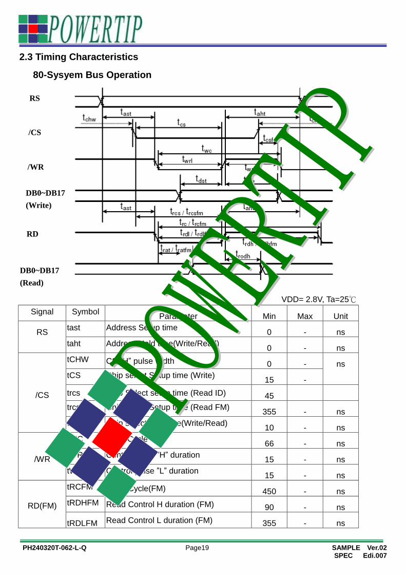
2.3 Timing Characteristics
80-Sysyem Bus Operation VDD= 2.8V, Ta=25℃
Signal Symbol Parameter Min Max Unit
RS tast Address Setup time 0 - ns taht Address Hold time(Write/Read) 0 - ns
/CS
tCHW CS “H” pulse width 0 - ns tCS Chip select Setup time (Write) 15 - trcs Chip Select setup time (Read ID) 45 trcsfm Chip select Setup time (Read FM) 355 - ns tCSF Chip select wait time(Write/Read) 10 - ns
/WR
tWC Write Cycle 66 - ns tWRH Control pulse ”H” duration 15 - ns tWRL Control pulse ”L” duration 15 - ns
RD(FM)
tRCFM Read Cycle(FM) 450 - ns tRDHFM Read Control H duration (FM) 90 - ns
tRDLFM Read Control L duration (FM) 355 - ns
DB0~DB17 (Read)
/CS
/WR
RS
RD
DB0~DB17 (Write)

PH240320T-062-L-Q Page20 SAMPLE Ver.02
SPEC Edi.007
RD(ID)
trc Read Cycle(ID) 160 ns
trdh Read Control pulse H duration 90 ns
trdl Read Control pulse L duration 45 ns
DB0~DB17
tDST Write Data setup time 10 ns
tDHT Write Data hold time 10 ns
tRAT Read access time 40 ns
tRATFM Read access time - 340 ns
tODH Read Output disable time 20 80 ns
PH240320T-062-L-Q Page21 SAMPLE Ver.02
SPEC Edi.007
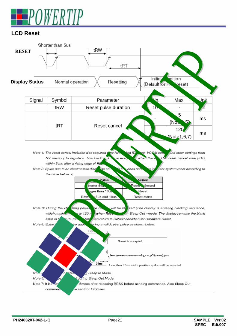
LCD Reset
Signal Symbol Parameter Min. Max. Unit tRW Reset pulse duration 10 - us
tRT Reset cancel -
5 (Note1,5)
ms
- 120
(Note1,6,7) ms
RESET
Display Status
PH240320T-062-L-Q Page22 SAMPLE Ver.02
SPEC Edi.007
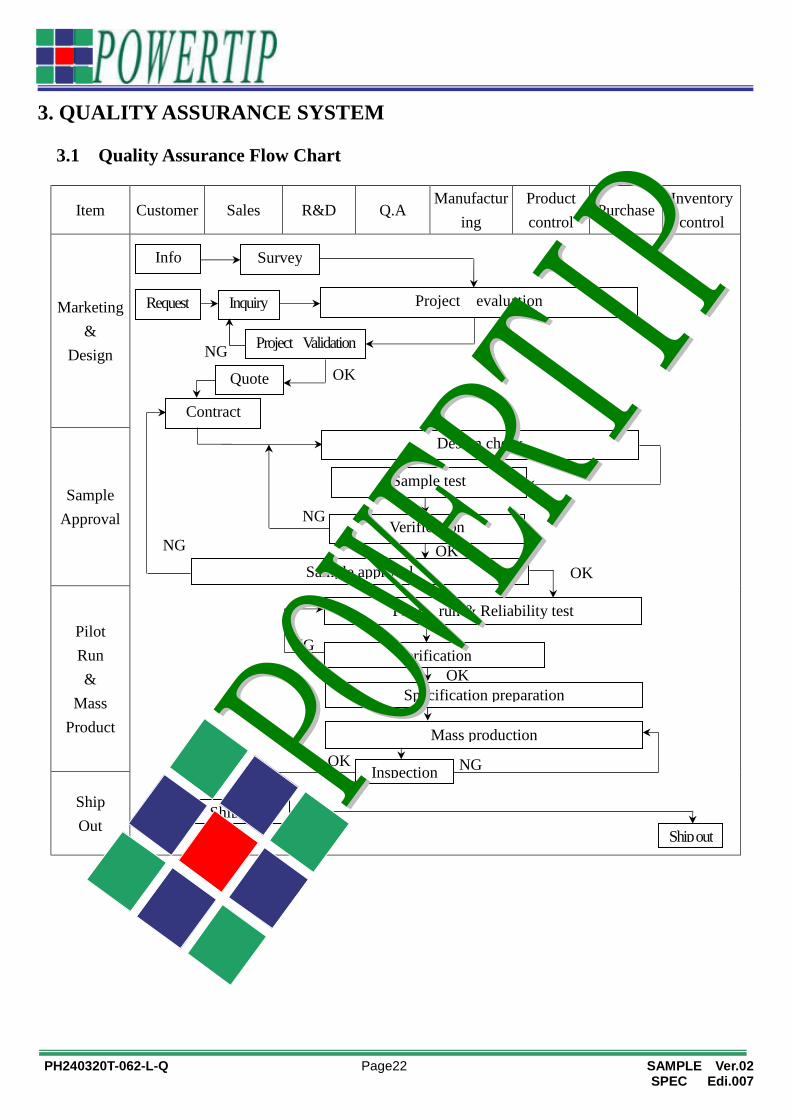
3. QUALITY ASSURANCE SYSTEM
3.1 Quality Assurance Flow Chart
Item Customer Sales R&D Q.A Manufactur
ing Product control
Purchase Inventory
control
Marketing &
Design
Sample Approval
Pilot Run &
Mass Product
Ship Out
OK
Request
Info Survey
Inquiry Project evaluation
Project Validation
Quote OK NG
Contract
Design check
Sample test
Verification
Sample approval
NG
NG
Pilot run & Reliability test
Verification
Specification preparation OK
Mass production
Inspection NG OK
Shipment
NG
Ship out
OK
PH240320T-062-L-Q Page23 SAMPLE Ver.02
SPEC Edi.007
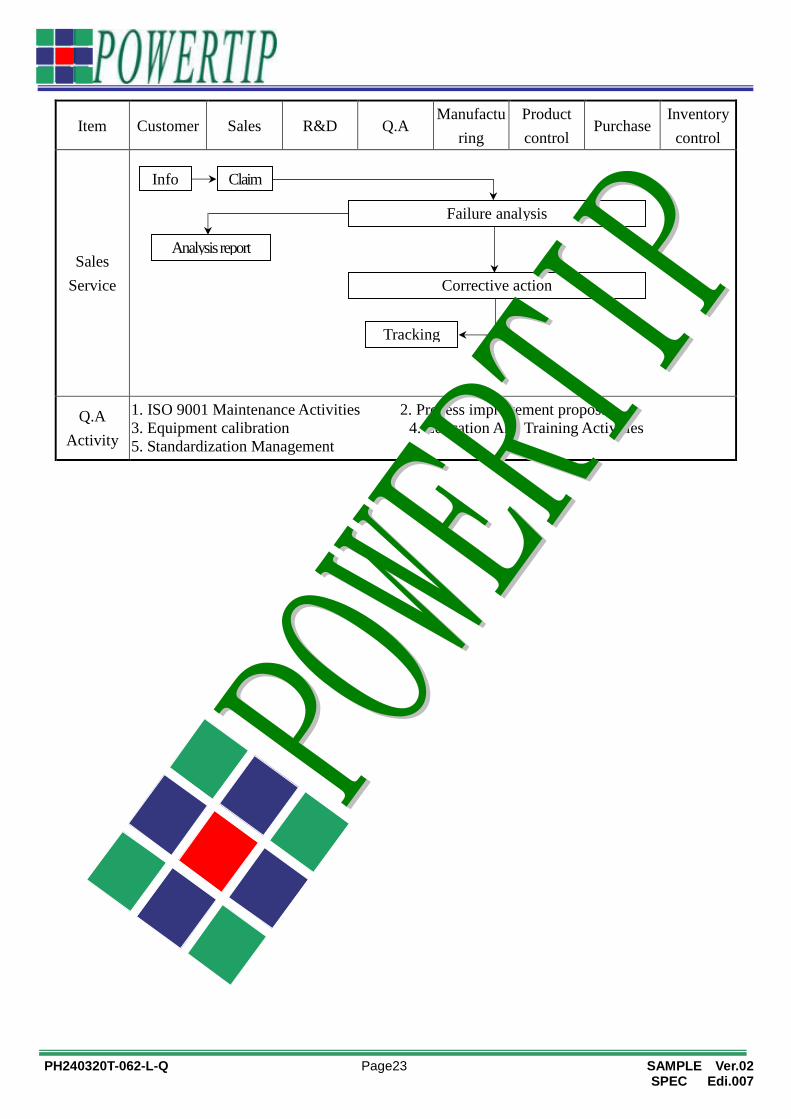
Item Customer Sales R&D Q.A Manufactu
ring Product control
Purchase Inventory
control
Sales Service
Q.A Activity
1. ISO 9001 Maintenance Activities 2. Process improvement proposal 3. Equipment calibration 4. Education And Training Activities 5. Standardization Management
Info Claim
Failure analysis
Corrective action
Tracking
Analysis report
PH240320T-062-L-Q Page24 SAMPLE Ver.02
SPEC Edi.007
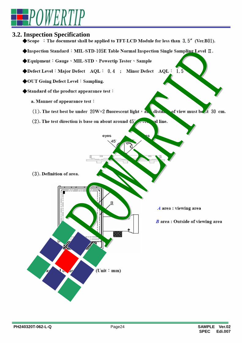
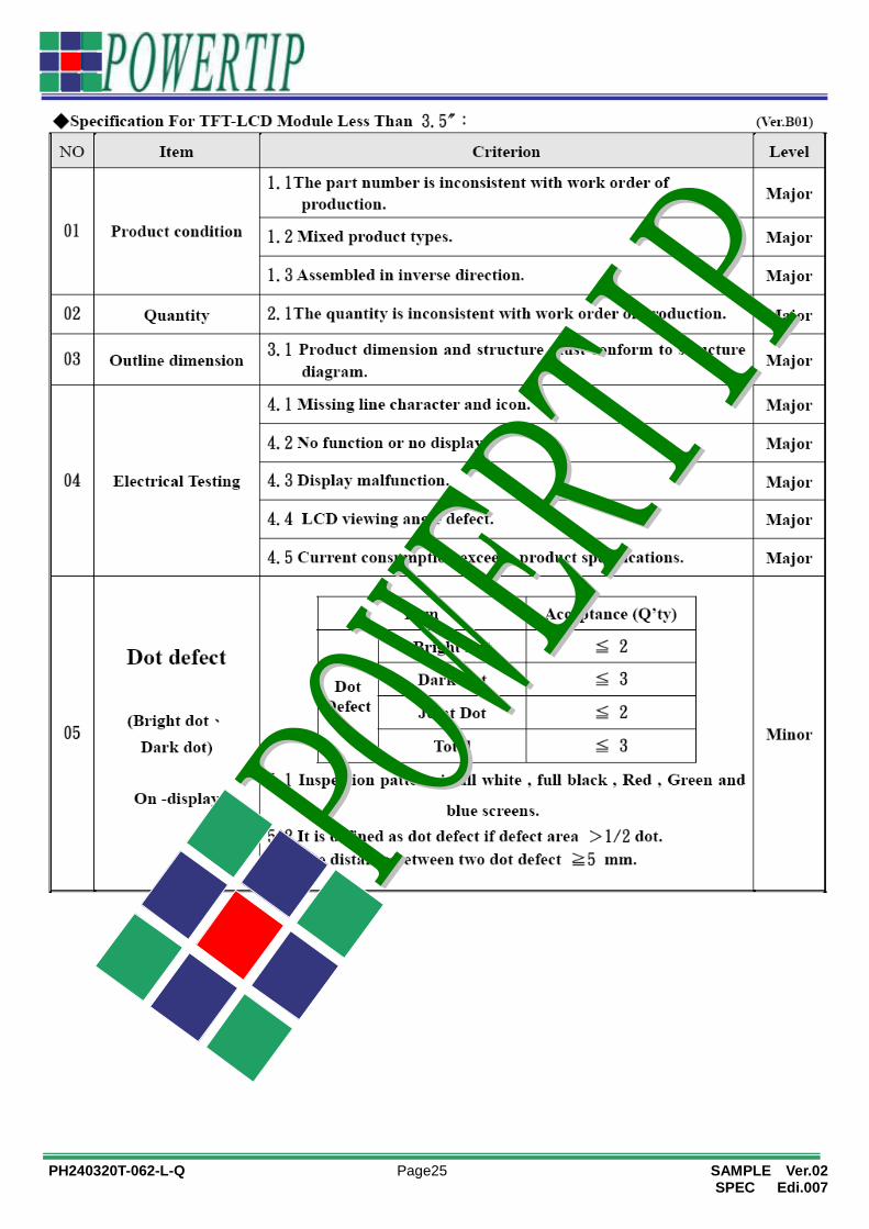
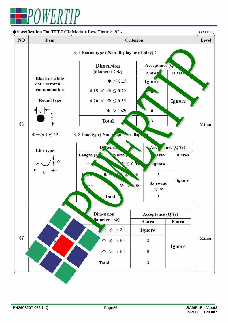
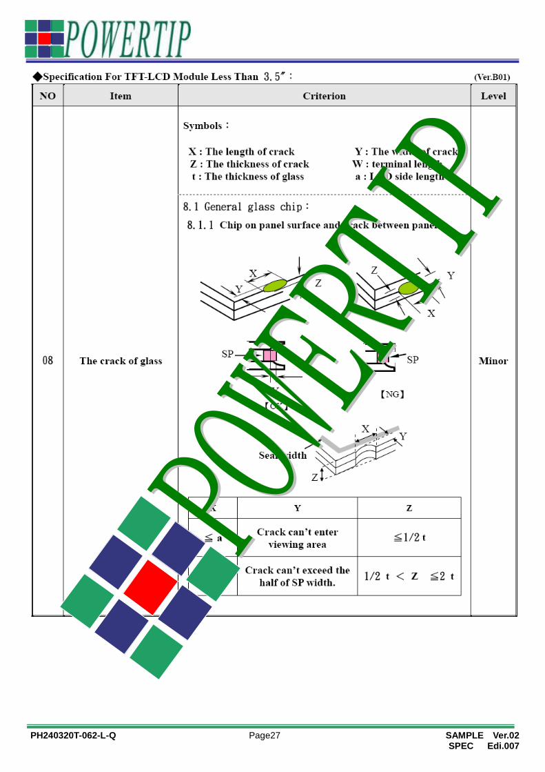
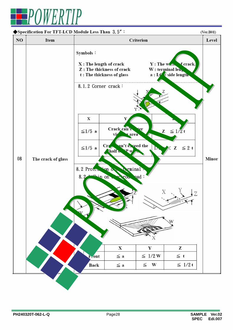
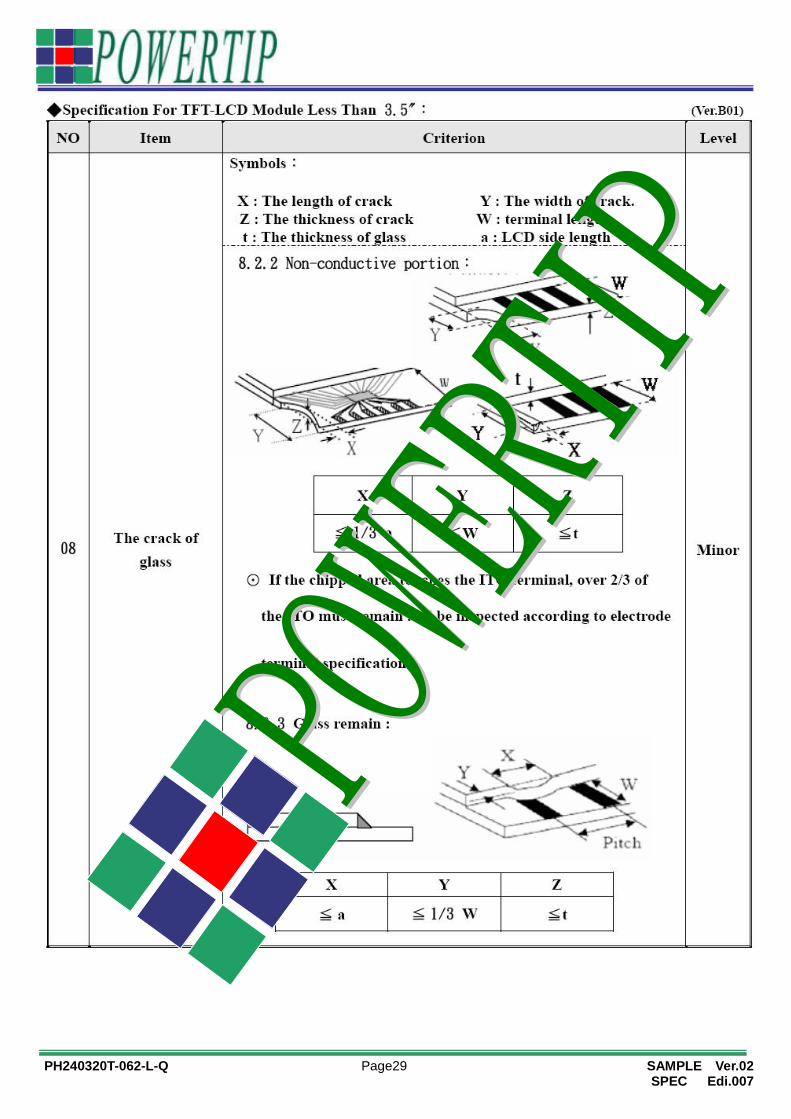
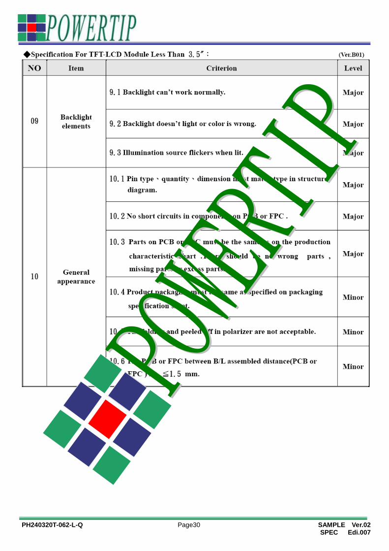
3.2. Inspection Specification
PH240320T-062-L-Q Page25 SAMPLE Ver.02
SPEC Edi.007
PH240320T-062-L-Q Page26 SAMPLE Ver.02
SPEC Edi.007
PH240320T-062-L-Q Page27 SAMPLE Ver.02
SPEC Edi.007
PH240320T-062-L-Q Page28 SAMPLE Ver.02
SPEC Edi.007
PH240320T-062-L-Q Page29 SAMPLE Ver.02
SPEC Edi.007
PH240320T-062-L-Q Page30 SAMPLE Ver.02
SPEC Edi.007
PH240320T-062-L-Q Page31 SAMPLE Ver.02
SPEC Edi.007
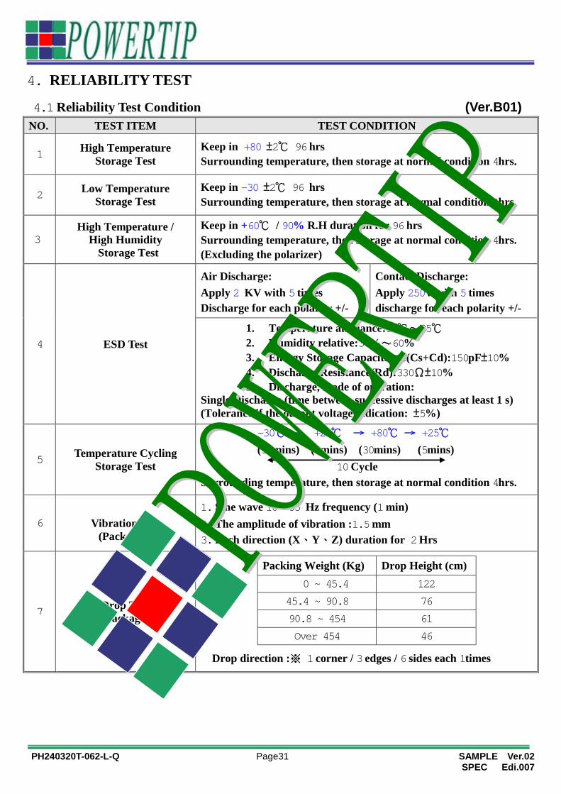
4. RELIABILITY TEST
4.1 Reliability Test Condition (Ver.B01) NO. TEST ITEM TEST CONDITION
1 High Temperature
Storage Test Keep in +80 ±2℃ 96 hrs Surrounding temperature, then storage at normal condition 4hrs.
2 Low Temperature
Storage Test Keep in -30 ±2℃ 96 hrs Surrounding temperature, then storage at normal condition 4hrs.
3 High Temperature /
High Humidity Storage Test
Keep in +60℃ / 90% R.H duration for 96 hrs Surrounding temperature, then storage at normal condition 4hrs. (Excluding the polarizer)
4 ESD Test
Air Discharge: Apply 2 KV with 5 times Discharge for each polarity +/-
Contact Discharge: Apply 250V with 5 times discharge for each polarity +/-
1. Temperature ambiance:15℃~35℃ 2. Humidity relative:30%~60% 3. Energy Storage Capacitance(Cs+Cd):150pF±10% 4. Discharge Resistance(Rd):330Ω±10% 5. Discharge, mode of operation:
Single Discharge (time between successive discharges at least 1 s) (Tolerance if the output voltage indication: ±5%)
5 Temperature Cycling
Storage Test
-30℃ → +25℃ → +80℃ → +25℃ (30mins) (5mins) (30mins) (5mins)
10 Cycle Surrounding temperature, then storage at normal condition 4hrs.
6
Vibration Test (Packaged)
1. Sine wave 10~55 Hz frequency (1 min) 2. The amplitude of vibration :1.5 mm 3. Each direction (X、Y、Z) duration for 2 Hrs
7 Drop Test
(Packaged)
Drop direction :※ 1 corner / 3 edges / 6 sides each 1times
Packing Weight (Kg) Drop Height (cm) 0 ~ 45.4 122
45.4 ~ 90.8 76
90.8 ~ 454 61
Over 454 46
PH240320T-062-L-Q Page32 SAMPLE Ver.02
SPEC Edi.007
5. PRECAUTION RELATING PRODUCT HANDLING 5.1 SAFETY
5.1.1 If the LCD panel breaks , be careful not to get the liquid crystal to touch your skin. 5.1.2 If the liquid crystal touches your skin or clothes , please wash it off immediately by
using soap and water. 5.2 HANDLING
5.2.1 Avoid any strong mechanical shock which can break the glass. 5.2.2 Avoid static electricity which can damage the CMOS LSI—When working with the
module , be sure to ground your body and any electrical equipment you may be using. 5.2.3 Do not remove the panel or frame from the module.
5.2.4 The polarizing plate of the display is very fragile. So , please handle it very carefully ,do not touch , push or rub the exposed polarizing with anything harder than an HB pencil lead (glass , tweezers , etc.)
5.2.5 Do not wipe the polarizing plate with a dry cloth , as it may easily scratch the surface of plate.
5.2.6 Do not touch the display area with bare hands , this will stain the display area. 5.2.7 Do not use ketonics solvent & aromatic solvent. Use with a soft cloth soaked with
a cleaning naphtha solvent. 5.2.8 To control temperature and time of soldering is 320±10℃and 3-5 sec. 5.2.9 To avoid liquid (include organic solvent) stained on LCM .
5.3 STORAGE 5.3.1 Store the panel or module in a dark place where the temperature is 25℃ ±5℃
and the humidity is below 65% RH. 5.3.2 Do not place the module near organics solvents or corrosive gases.
5.3.3 Do not crush , shake , or jolt the module. 5.4 TERMS OF WARRANTY
5.4.1 Applicable warrant period The period is within Twenty-four months since the date of shipping out under normal using and storage conditions.
5.4.2 Unaccepted responsibility This product has been manufactured to your company’s specification as a part for use in your company’s general electronic products. It is guaranteed to perform according to delivery specifications. For any other use apart from general electronic equipment , we cannot take responsibility if the product is used in nuclear power control equipment , aerospace equipment , fire and security systems or any other applications in which there is a direct risk to human life and where extremely high levels of reliability are required.