Embed Size (px)
Citation preview
MCM & LTCC TECHNOLOGY MCM & LTCC TECHNOLOGY FOR MICROELECTRONICSFOR MICROELECTRONICS
TECTEC--ENC 13ENC 13
TECTEC--ENC 13ENC 13-- 22
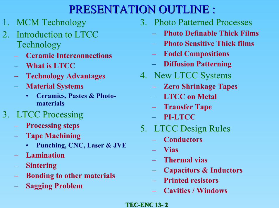
PRESENTATION OUTLINE :PRESENTATION OUTLINE :1. MCM Technology2. Introduction to LTCC
Technology– Ceramic Interconnections– What is LTCC– Technology Advantages– Material Systems
• Ceramics, Pastes & Photo-materials
3. LTCC Processing– Processing steps– Tape Machining
• Punching, CNC, Laser & JVE– Lamination– Sintering– Bonding to other materials– Sagging Problem
3. Photo Patterned Processes– Photo Definable Thick Films– Photo Sensitive Thick films– Fodel Compositions– Diffusion Patterning
4. New LTCC Systems– Zero Shrinkage Tapes– LTCC on Metal– Transfer Tape – PI-LTCC
5. LTCC Design Rules– Conductors– Vias– Thermal vias– Capacitors & Inductors– Printed resistors– Cavities / Windows
TECTEC--ENC 13ENC 13-- 33
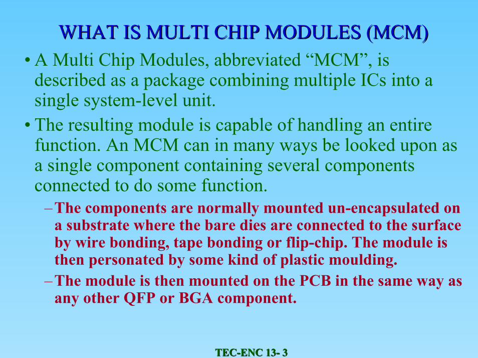
WHAT IS MULTI CHIP MODULES (MCM)WHAT IS MULTI CHIP MODULES (MCM)• A Multi Chip Modules, abbreviated “MCM”, is
described as a package combining multiple ICs into a single system-level unit.
• The resulting module is capable of handling an entire function. An MCM can in many ways be looked upon as a single component containing several components connected to do some function.
–The components are normally mounted un-encapsulated ona substrate where the bare dies are connected to the surface by wire bonding, tape bonding or flip-chip. The module isthen personated by some kind of plastic moulding.
–The module is then mounted on the PCB in the same way asany other QFP or BGA component.
TECTEC--ENC 13ENC 13-- 44
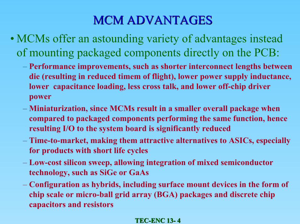
MCM ADVANTAGESMCM ADVANTAGES• MCMs offer an astounding variety of advantages instead
of mounting packaged components directly on the PCB:– Performance improvements, such as shorter interconnect lengths between
die (resulting in reduced timem of flight), lower power supply inductance,lower capacitance loading, less cross talk, and lower off-chip driver power
– Miniaturization, since MCMs result in a smaller overall package when compared to packaged components performing the same function, hence resulting I/O to the system board is significantly reduced
– Time-to-market, making them attractive alternatives to ASICs, especiallyfor products with short life cycles
– Low-cost silicon sweep, allowing integration of mixed semiconductor technology, such as SiGe or GaAs
– Configuration as hybrids, including surface mount devices in the form of chip scale or micro-ball grid array (BGA) packages and discrete chipcapacitors and resistors

TECTEC--ENC 13ENC 13-- 55
MCM ADVANTAGESMCM ADVANTAGES–Simplification of board complexity by sweeping several devices
onto one package, thereby by reducing total opportunities forerror at the board assembly level, as well as allowing for acheaper PCB
– Improved reliability by decreasing the number of interconnects between “components” and boards
–Adding new functions to a fixed footprint–Capability of accommodating a variety of second-level
interconnects. While BGA are the most popular, lead-framesolutions can be employed for plugability, enabling modularityfor upgrades.

TECTEC--ENC 13ENC 13-- 66
MCM DISADVANTAGESMCM DISADVANTAGES• Although there is many good reasons for using MCMs, there are also some difficulties and disadvantages.
–The most important problem that hinders a morewidespread use is the availability of components in “Bare Die” form. Although the market is improving, there is still a long way to go before most components areavailable as “Bare Dies”.
–The other concern is cost. Although the newer MCM-Ltechnologies have a low cost potential, cost is rarely the solereason for going into MCMs.
TECTEC--ENC 13ENC 13-- 77
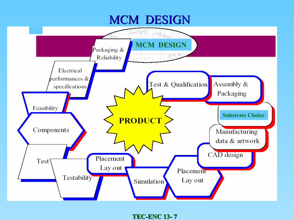
MCM DESIGN MCM DESIGN
MCM DESIGN
Substrate Choice
TECTEC--ENC 13ENC 13-- 88
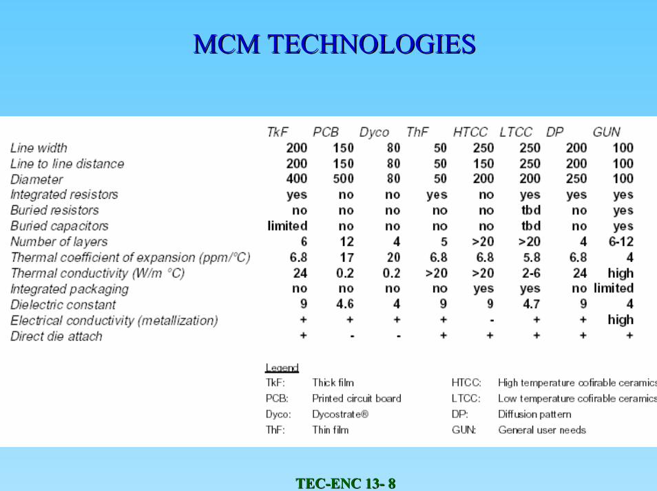
MCM TECHNOLOGIESMCM TECHNOLOGIES
TECTEC--ENC 13ENC 13-- 99
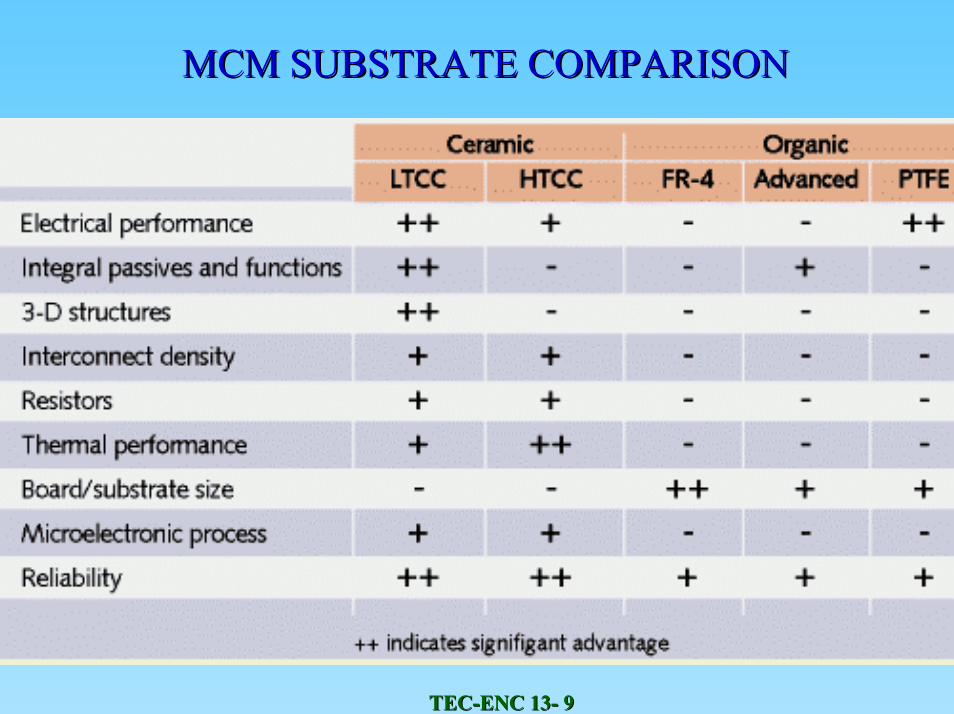
MCM SUBSTRATE COMPARISONMCM SUBSTRATE COMPARISON
INTRODUCTION TO LTCC TECHNOLOGYINTRODUCTION TO LTCC TECHNOLOGY
–– Ceramic InterconnectionsCeramic Interconnections–– What is LTCCWhat is LTCC–– Technology AdvantagesTechnology Advantages–– Material SystemsMaterial Systems
•• CeramicsCeramics•• Pastes Pastes •• PhotoPhoto--materialsmaterials

TECTEC--ENC 13ENC 13-- 1111
CERAMIC INTERCONNECT TECHNOLOGYCERAMIC INTERCONNECT TECHNOLOGY
Source: Green Tape Application Group
PI-LTCC
TECTEC--ENC 13ENC 13-- 1212
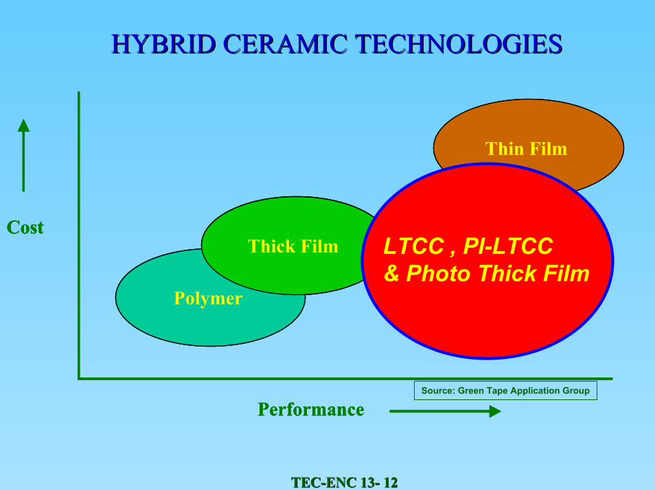
HYBRID CERAMIC TECHNOLOGIESHYBRID CERAMIC TECHNOLOGIES
Cost
Performance
Polymer
Thick Film
Thin Film
Cost
Performance
Polymer
Thick Film
Thin Film
Cost
Performance
Polymer
Thick Film
Source: Green Tape Application Group
LTCC , PI-LTCC& Photo Thick Film
TECTEC--ENC 13ENC 13-- 1313
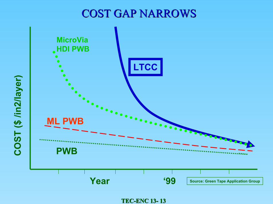
COST GAP NARROWSCOST GAP NARROWS
LTCC
CO
ST ($
/in2
/laye
r)
Year ‘99
PWB
ML PWB
MicroVia HDI PWB
Source: Green Tape Application Group
TECTEC--ENC 13ENC 13-- 1414
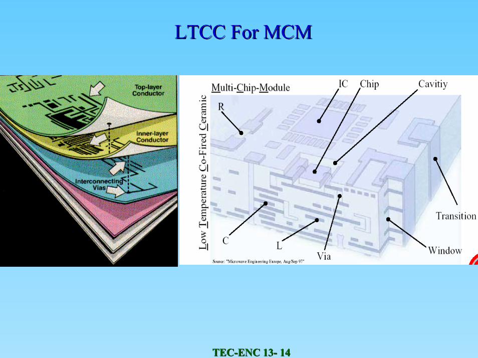
LTCC For MCMLTCC For MCM
TECTEC--ENC 13ENC 13-- 1515
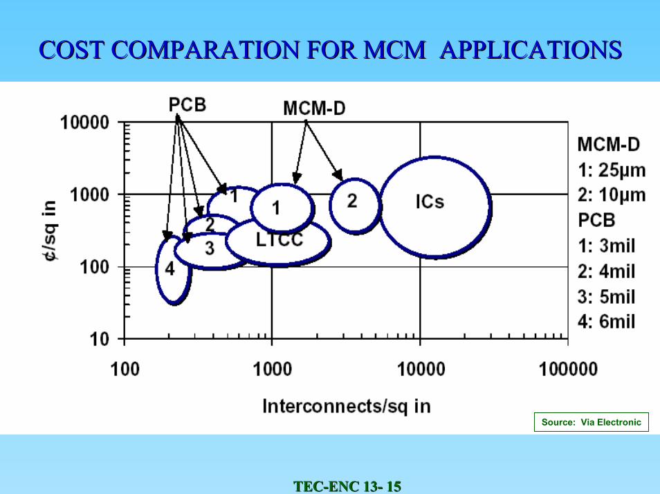
COST COMPARATION FOR MCM APPLICATIONSCOST COMPARATION FOR MCM APPLICATIONS
Source: Via Electronic
TECTEC--ENC 13ENC 13-- 1616
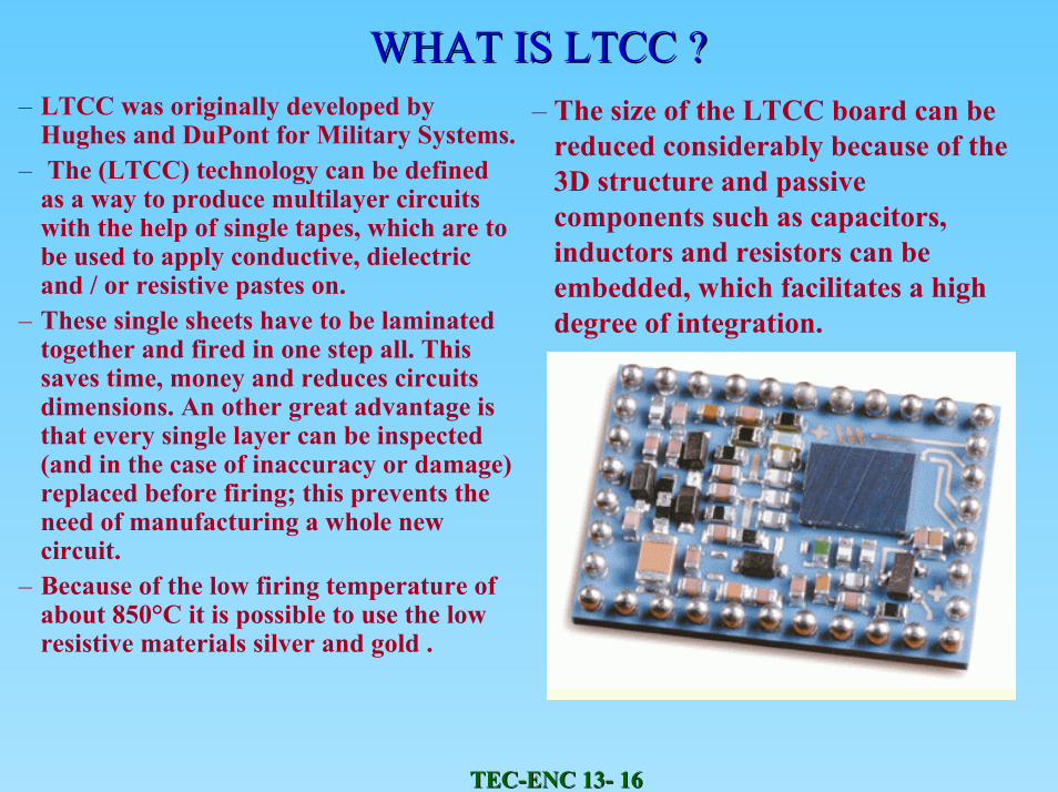
WHAT IS LTCC ?WHAT IS LTCC ?– LTCC was originally developed by
Hughes and DuPont for Military Systems. – The (LTCC) technology can be defined
as a way to produce multilayer circuits with the help of single tapes, which are to be used to apply conductive, dielectric and / or resistive pastes on.
– These single sheets have to be laminated together and fired in one step all. This saves time, money and reduces circuits dimensions. An other great advantage is that every single layer can be inspected (and in the case of inaccuracy or damage) replaced before firing; this prevents the need of manufacturing a whole new circuit.
– Because of the low firing temperature of about 850°C it is possible to use the low resistive materials silver and gold .
– The size of the LTCC board can be reduced considerably because of the 3D structure and passive components such as capacitors, inductors and resistors can be embedded, which facilitates a high degree of integration.
TECTEC--ENC 13ENC 13-- 1717
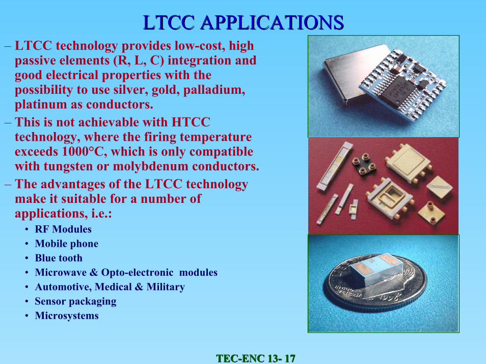
LTCC APPLICATIONSLTCC APPLICATIONS– LTCC technology provides low-cost, high
passive elements (R, L, C) integration and good electrical properties with the possibility to use silver, gold, palladium, platinum as conductors.
– This is not achievable with HTCC technology, where the firing temperature exceeds 1000°C, which is only compatible with tungsten or molybdenum conductors.
– The advantages of the LTCC technology make it suitable for a number of applications, i.e.:
• RF Modules • Mobile phone• Blue tooth• Microwave & Opto-electronic modules• Automotive, Medical & Military• Sensor packaging• Microsystems
TECTEC--ENC 13ENC 13-- 1818
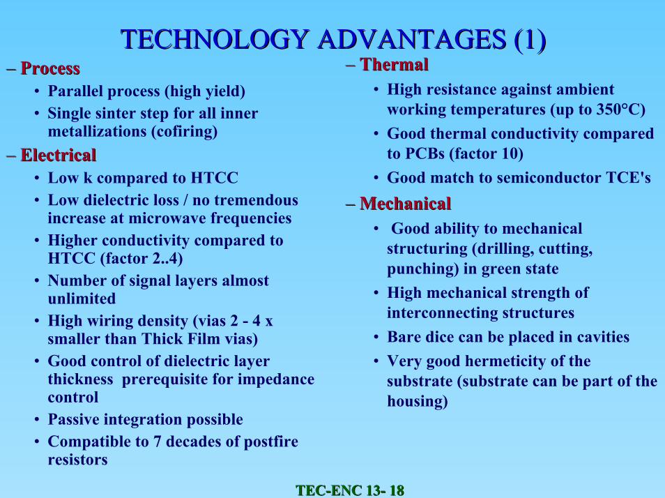
TECHNOLOGY ADVANTAGES (1)TECHNOLOGY ADVANTAGES (1)–– Process Process
• Parallel process (high yield) • Single sinter step for all inner
metallizations (cofiring) –– Electrical Electrical
• Low k compared to HTCC • Low dielectric loss / no tremendous
increase at microwave frequencies • Higher conductivity compared to
HTCC (factor 2..4) • Number of signal layers almost
unlimited • High wiring density (vias 2 - 4 x
smaller than Thick Film vias) • Good control of dielectric layer
thickness prerequisite for impedance control
• Passive integration possible • Compatible to 7 decades of postfire
resistors
–– Thermal Thermal • High resistance against ambient
working temperatures (up to 350°C) • Good thermal conductivity compared
to PCBs (factor 10) • Good match to semiconductor TCE's
–– MechanicalMechanical• Good ability to mechanical
structuring (drilling, cutting, punching) in green state
• High mechanical strength of interconnecting structures
• Bare dice can be placed in cavities • Very good hermeticity of the
substrate (substrate can be part of the housing)
TECTEC--ENC 13ENC 13-- 1919
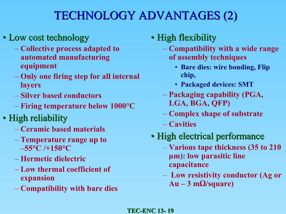
TECHNOLOGY ADVANTAGES (2)TECHNOLOGY ADVANTAGES (2)
•• Low cost technologyLow cost technology– Collective process adapted to
automated manufacturingequipment
– Only one firing step for all internal layers
– Silver based conductors– Firing temperature below 1000°C
•• High reliabilityHigh reliability– Ceramic based materials– Temperature range up to
–55°C /+150°C– Hermetic dielectric– Low thermal coefficient of
expansion– Compatibility with bare dies
•• High flexibilityHigh flexibility– Compatibility with a wide range
of assembly techniques• Bare dies: wire bonding, Flip
chip,• Packaged devices: SMT
– Packaging capability (PGA, LGA, BGA, QFP)
– Complex shape of substrate– Cavities
•• High electrical performanceHigh electrical performance– Various tape thickness (35 to 210
µm): low parasitic line capacitance
– Low resistivity conductor (Ag or Au – 3 mΩ/square)
TECTEC--ENC 13ENC 13-- 2020
TECHNOLOGY ADVANTAGES (3)TECHNOLOGY ADVANTAGES (3)
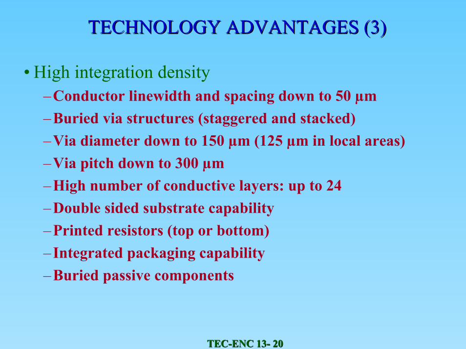
• High integration density–Conductor linewidth and spacing down to 50 µm–Buried via structures (staggered and stacked)–Via diameter down to 150 µm (125 µm in local areas)–Via pitch down to 300 µm–High number of conductive layers: up to 24–Double sided substrate capability–Printed resistors (top or bottom)– Integrated packaging capability–Buried passive components
TECTEC--ENC 13ENC 13-- 2121
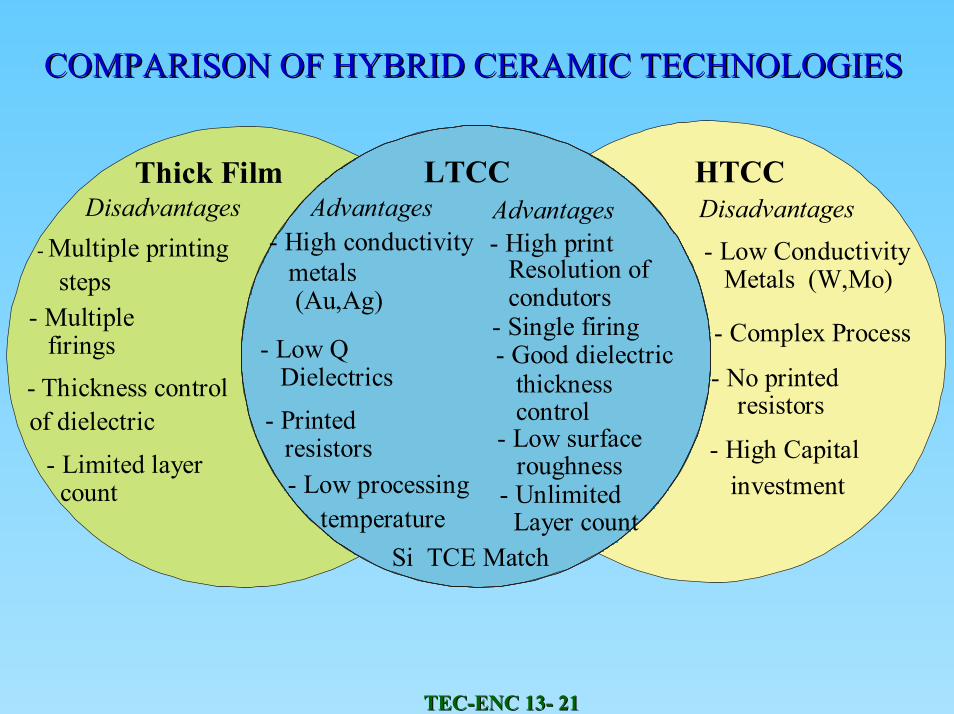
COMPARISON OF HYBRID CERAMIC TECHNOLOGIESCOMPARISON OF HYBRID CERAMIC TECHNOLOGIES
Thick Film HTCCLTCCDisadvantages DisadvantagesAdvantages Advantages
- Multiple printing steps
- Multiple firings
- Thickness control of dielectric
- Limited layer count
- Low Conductivity Metals (W,Mo)
- Complex Process
- No printed resistors
- High Capital investment
- High conductivity metals (Au,Ag)
- Low Q Dielectrics
- Printed resistors
- Low processing temperature
- High print Resolution of condutors- Single firing- Good dielectric thickness control- Low surface roughness- Unlimited Layer count
Si TCE Match
TECTEC--ENC 13ENC 13-- 2222
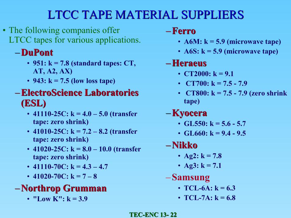
LTCC TAPE MATERIAL SUPPLIERSLTCC TAPE MATERIAL SUPPLIERS–– Ferro Ferro
• A6M: k = 5.9 (microwave tape) • A6S: k = 5.9 (microwave tape)
–– HeraeusHeraeus• CT2000: k = 9.1 • CT700: k = 7.5 - 7.9 • CT800: k = 7.5 - 7.9 (zero shrink
tape)
–– Kyocera Kyocera • GL550: k = 5.6 - 5.7 • GL660: k = 9.4 - 9.5
–– Nikko Nikko • Ag2: k = 7.8 • Ag3: k = 7.1
–Samsung • TCL-6A: k = 6.3 • TCL-7A: k = 6.8
• The following companies offer LTCC tapes for various applications.
–– DuPont DuPont • 951: k = 7.8 (standard tapes: CT,
AT, A2, AX) • 943: k = 7.5 (low loss tape)
–– ElectroScienceElectroScience Laboratories Laboratories (ESL)(ESL)
• 41110-25C: k = 4.0 – 5.0 (transfer tape: zero shrink)
• 41010-25C: k = 7.2 – 8.2 (transfer tape: zero shrink)
• 41020-25C: k = 8.0 – 10.0 (transfer tape: zero shrink)
• 41110-70C: k = 4.3 – 4.7 • 41020-70C: k = 7 – 8
–– Northrop Grumman Northrop Grumman • "Low K": k = 3.9
TECTEC--ENC 13ENC 13-- 2323
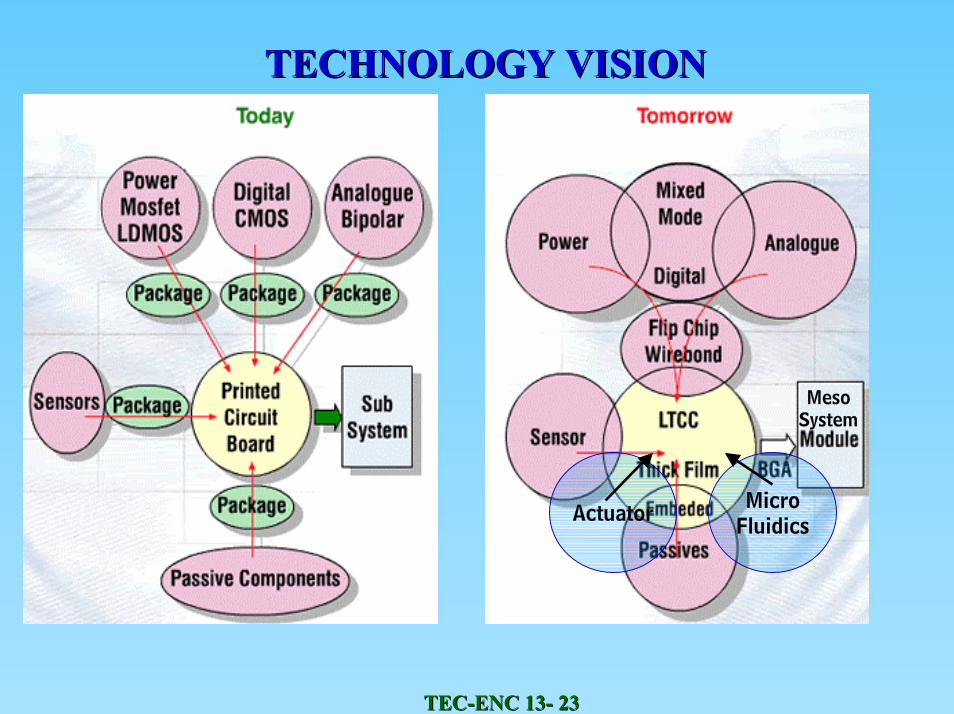
TECHNOLOGY VISIONTECHNOLOGY VISION
Meso System
Actuator Micro Fluidics
TECTEC--ENC 13ENC 13-- 2424
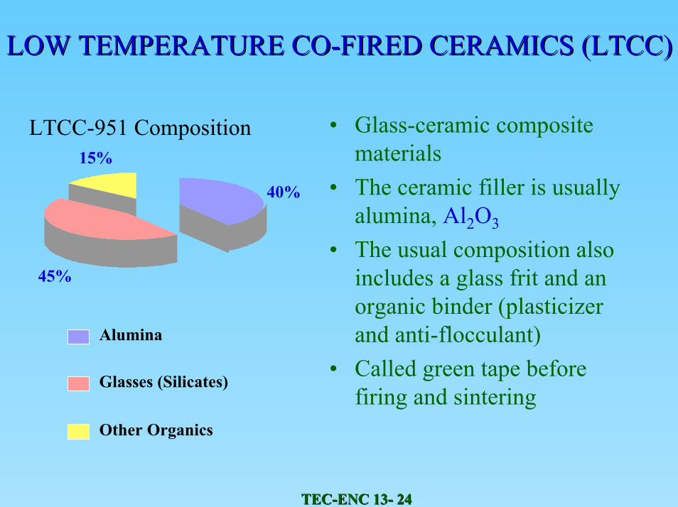
LOW TEMPERATURE COLOW TEMPERATURE CO--FIRED CERAMICS (LTCC)FIRED CERAMICS (LTCC)
• Glass-ceramic composite materials
• The ceramic filler is usually alumina, Al2O3
• The usual composition also includes a glass frit and an organic binder (plasticizerand anti-flocculant)
• Called green tape before firing and sintering
LTCC-951 Composition
40%
45%
15%
Alumina
Glasses (Silicates)
Other Organics
TECTEC--ENC 13ENC 13-- 2525
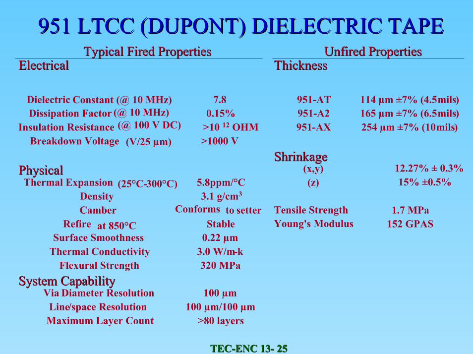
951 LTCC (DUPONT) DIELECTRIC TAPE951 LTCC (DUPONT) DIELECTRIC TAPETypical Fired PropertiesTypical Fired Properties Unfired PropertiesUnfired Properties
ElectricalElectrical ThicknessThickness
Dielectric Constant (@ 10 MHz) 7.8 951-AT 114 µm ±7% (4.5mils)Dissipation Factor (@ 10 MHz) 0.15% 951-A2 165 µm ±7% (6.5mils)
Insulation Resistance (@ 100 V DC) >10 12 OHM 951-AX 254 µm ±7% (10mils)Breakdown Voltage (V/25 µm) >1000 V
ShrinkageShrinkagePhysicalPhysical (x,y) 12.27% ± 0.3%Thermal Expansion (25°C-300°C) 5.8ppm/°C (z) 15% ±0.5%
Density 3.1 g/cm3
Camber Conforms to setter Tensile Strength 1.7 MPaRefire at 850°C Stable Young's Modulus 152 GPAS
Surface Smoothness 0.22 µmThermal Conductivity 3.0 W/m-k
Flexural Strength 320 MPaSystem CapabilitySystem Capability
Via Diameter Resolution 100 µmLine/space Resolution 100 µm/100 µm
Maximum Layer Count >80 layers
TECTEC--ENC 13ENC 13-- 2626
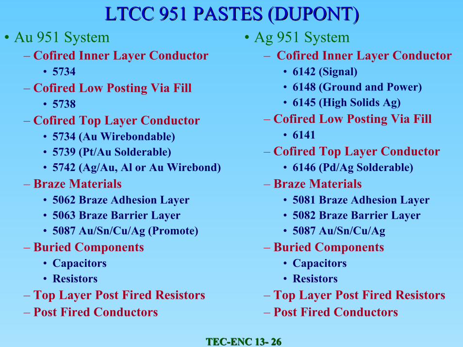
LTCC 951 PASTES (DUPONT) LTCC 951 PASTES (DUPONT) • Au 951 System
– Cofired Inner Layer Conductor• 5734
– Cofired Low Posting Via Fill• 5738
– Cofired Top Layer Conductor• 5734 (Au Wirebondable)• 5739 (Pt/Au Solderable)• 5742 (Ag/Au, Al or Au Wirebond)
– Braze Materials• 5062 Braze Adhesion Layer• 5063 Braze Barrier Layer• 5087 Au/Sn/Cu/Ag (Promote)
– Buried Components• Capacitors• Resistors
– Top Layer Post Fired Resistors– Post Fired Conductors
• Ag 951 System – Cofired Inner Layer Conductor
• 6142 (Signal)• 6148 (Ground and Power)• 6145 (High Solids Ag)
– Cofired Low Posting Via Fill• 6141
– Cofired Top Layer Conductor• 6146 (Pd/Ag Solderable)
– Braze Materials• 5081 Braze Adhesion Layer• 5082 Braze Barrier Layer• 5087 Au/Sn/Cu/Ag
– Buried Components • Capacitors• Resistors
– Top Layer Post Fired Resistors – Post Fired Conductors
TECTEC--ENC 13ENC 13-- 2727
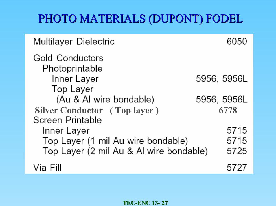
PHOTO MATERIALS (DUPONT) FODELPHOTO MATERIALS (DUPONT) FODEL
Silver Conductor ( Top layer ) 6778
TECTEC--ENC 13ENC 13-- 2828
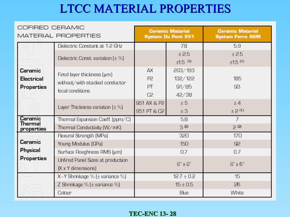
LTCC LTCC MATERIAL PROPERTIESMATERIAL PROPERTIES
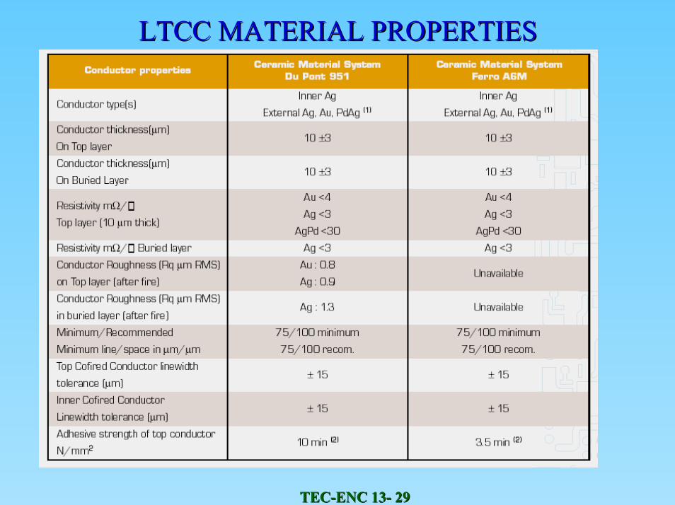
TECTEC--ENC 13ENC 13-- 2929
LTCC LTCC MATERIAL PROPERTIESMATERIAL PROPERTIES
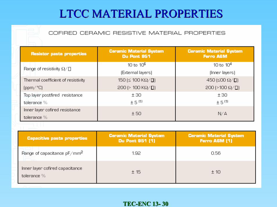
TECTEC--ENC 13ENC 13-- 3030
LTCC LTCC MATERIAL PROPERTIESMATERIAL PROPERTIES
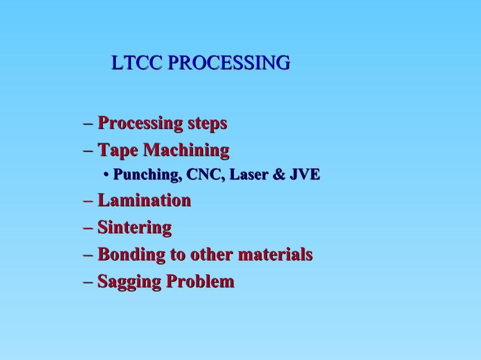
LTCC PROCESSINGLTCC PROCESSING
–– Processing stepsProcessing steps–– Tape MachiningTape Machining
•• Punching, CNC, Laser & JVEPunching, CNC, Laser & JVE
–– LaminationLamination–– SinteringSintering–– Bonding to other materialsBonding to other materials–– Sagging ProblemSagging Problem
TECTEC--ENC 13ENC 13-- 3232
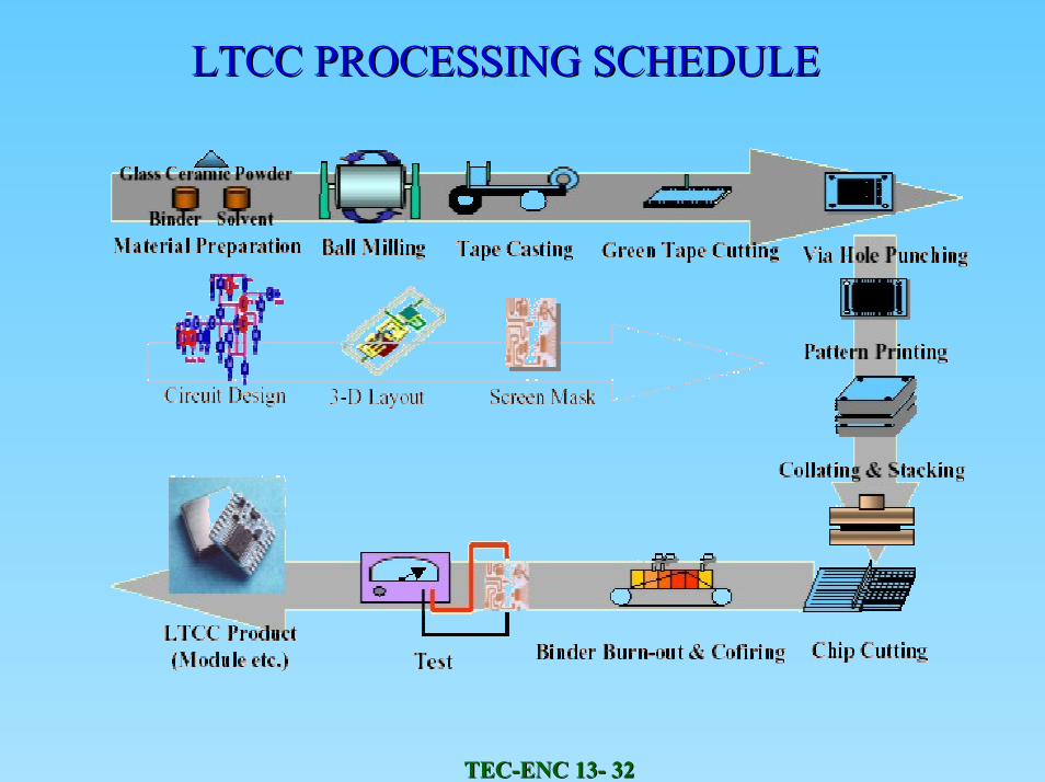
LTCC PROCESSING SCHEDULE LTCC PROCESSING SCHEDULE
TECTEC--ENC 13ENC 13-- 3333
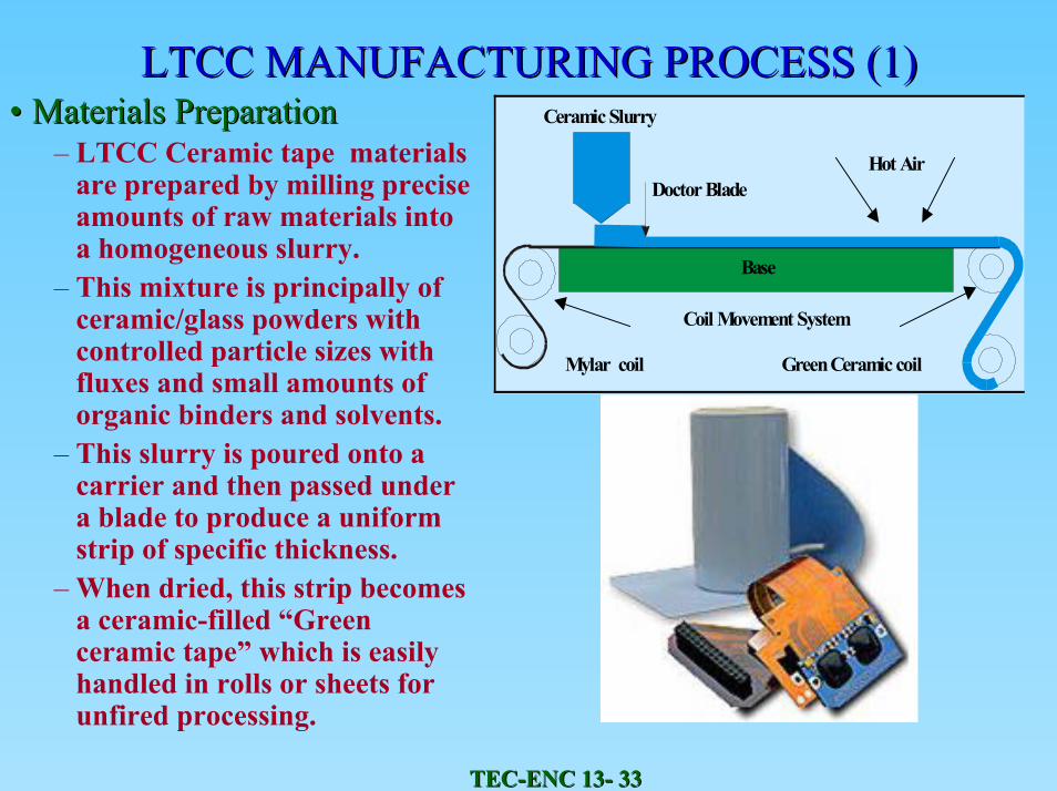
LTCC MANUFACTURING PROCESS (1)LTCC MANUFACTURING PROCESS (1)•• Materials PreparationMaterials Preparation
– LTCC Ceramic tape materials are prepared by milling precise amounts of raw materials into a homogeneous slurry.
– This mixture is principally of ceramic/glass powders with controlled particle sizes with fluxes and small amounts of organic binders and solvents.
– This slurry is poured onto a carrier and then passed under a blade to produce a uniform strip of specific thickness.
– When dried, this strip becomes a ceramic-filled “Green ceramic tape” which is easily handled in rolls or sheets for unfired processing.
Ceramic Slurry
Doctor BladeHot Air
Mylar coil Green Ceramic coil
Base
Coil Movement System
TECTEC--ENC 13ENC 13-- 3434
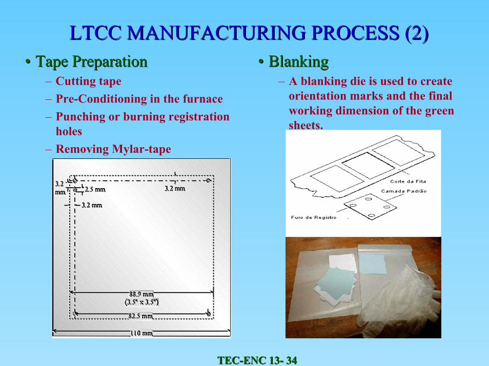
LTCC MANUFACTURING PROCESS (2)LTCC MANUFACTURING PROCESS (2)•• BlankingBlanking
– A blanking die is used to create orientation marks and the final working dimension of the green sheets.
•• Tape PreparationTape Preparation– Cutting tape – Pre-Conditioning in the furnace – Punching or burning registration
holes – Removing Mylar-tape
TECTEC--ENC 13ENC 13-- 3535
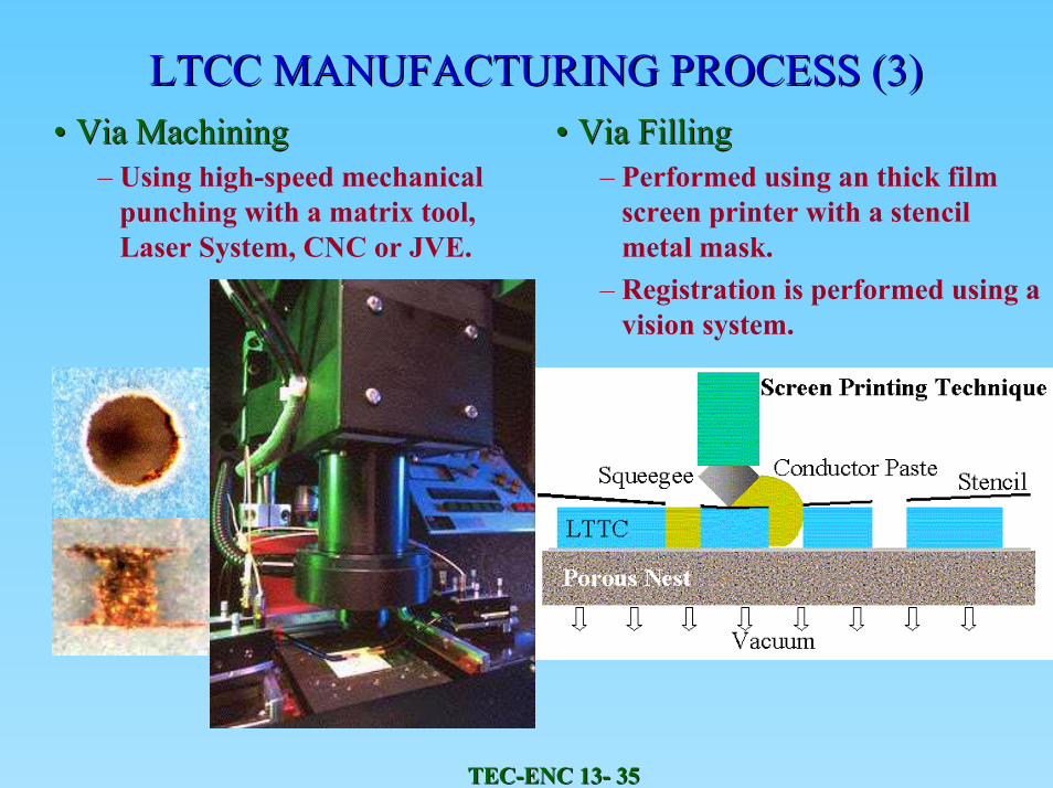
LTCC MANUFACTURING PROCESS (3)LTCC MANUFACTURING PROCESS (3)•• Via FillingVia Filling
– Performed using an thick film screen printer with a stencil metal mask.
– Registration is performed using a vision system.
•• Via MachiningVia Machining– Using high-speed mechanical
punching with a matrix tool, Laser System, CNC or JVE.
TECTEC--ENC 13ENC 13-- 3636
LTCC MANUFACTURING PROCESS (4)LTCC MANUFACTURING PROCESS (4)
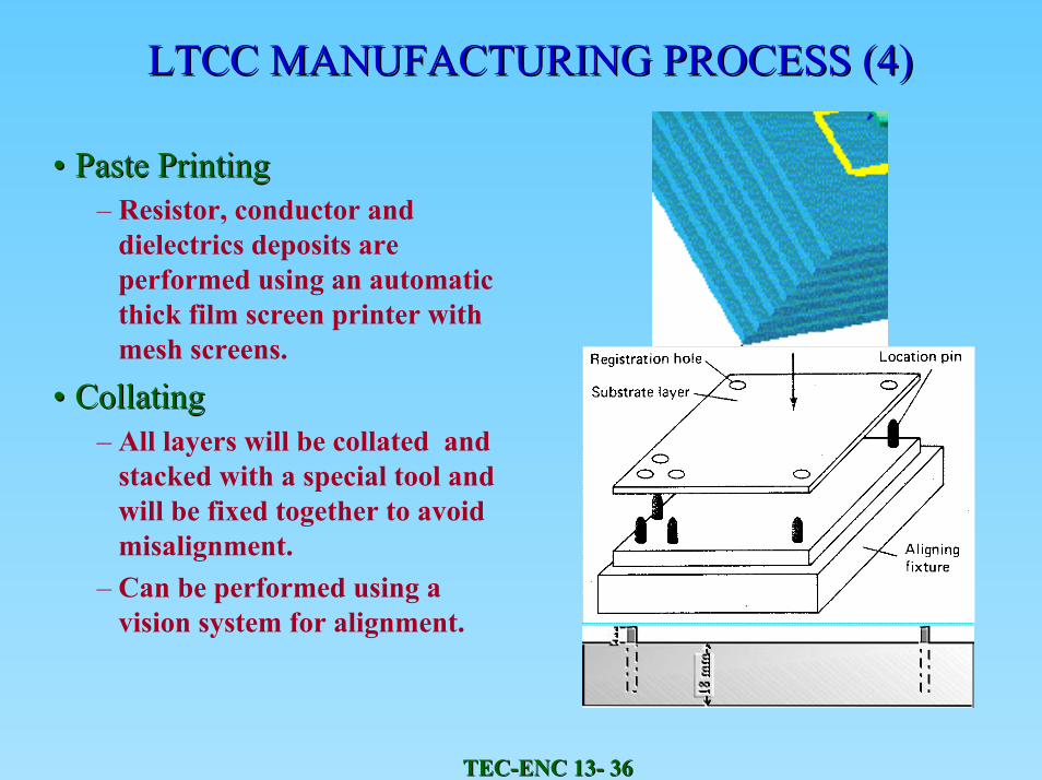
•• Paste PrintingPaste Printing– Resistor, conductor and
dielectrics deposits are performed using an automatic thick film screen printer with mesh screens.
•• CollatingCollating– All layers will be collated and
stacked with a special tool and will be fixed together to avoid misalignment.
– Can be performed using a vision system for alignment.
TECTEC--ENC 13ENC 13-- 3737
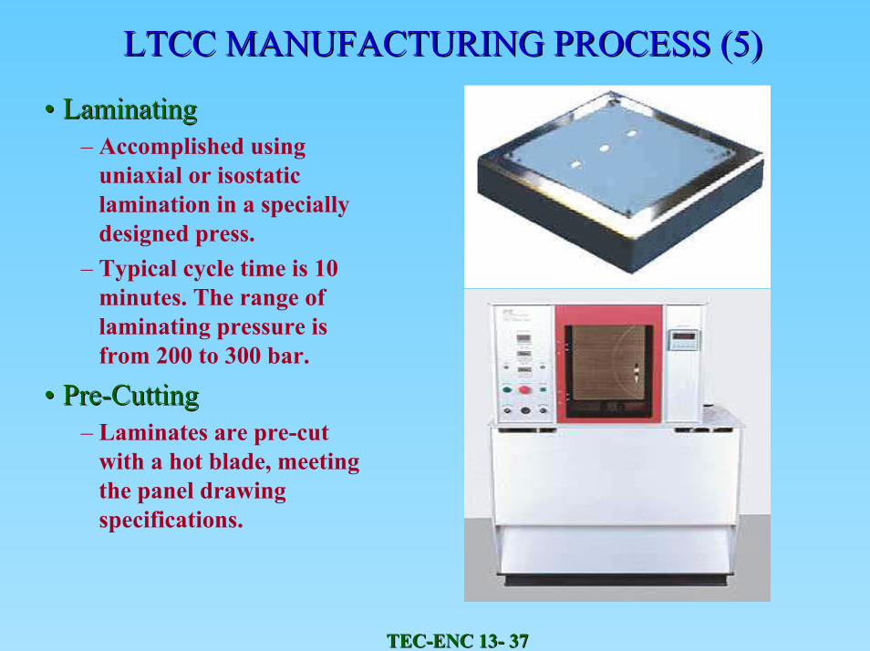
LTCC MANUFACTURING PROCESS (5)LTCC MANUFACTURING PROCESS (5)
•• LaminatingLaminating– Accomplished using
uniaxial or isostaticlamination in a specially designed press.
– Typical cycle time is 10 minutes. The range of laminating pressure is from 200 to 300 bar.
•• PrePre--CuttingCutting– Laminates are pre-cut
with a hot blade, meeting the panel drawing specifications.
TECTEC--ENC 13ENC 13-- 3838
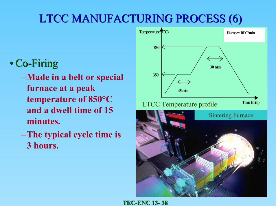
LTCC MANUFACTURING PROCESS (6)LTCC MANUFACTURING PROCESS (6)
850
350
Temperature (oC)
Time (min)
45 min
30 min
Ramp = 10oC/min
LTCC Temperature profile
•• CoCo--FiringFiring–Made in a belt or special
furnace at a peak temperature of 850°C and a dwell time of 15 minutes.
–The typical cycle time is 3 hours.
Sintering Furnace
TECTEC--ENC 13ENC 13-- 3939
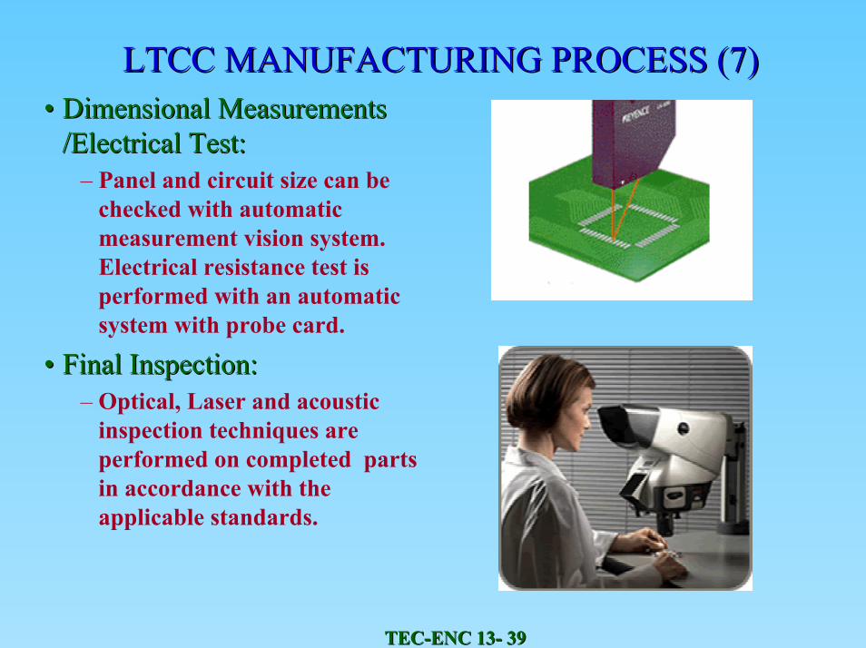
LTCC MANUFACTURING PROCESS (7)LTCC MANUFACTURING PROCESS (7)•• Dimensional Measurements Dimensional Measurements
/Electrical Test:/Electrical Test:– Panel and circuit size can be
checked with automatic measurement vision system. Electrical resistance test is performed with an automatic system with probe card.
•• Final Inspection:Final Inspection:– Optical, Laser and acoustic
inspection techniques are performed on completed parts in accordance with the applicable standards.
TECTEC--ENC 13ENC 13-- 4040
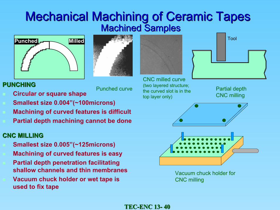
PUNCHINGPUNCHINGCircular or square shapeSmallest size 0.004”(~100microns)Machining of curved features is difficultPartial depth machining cannot be done
CNC MILLINGCNC MILLINGSmallest size 0.005”(~125microns)Machining of curved features is easy Partial depth penetration facilitating shallow channels and thin membranesVacuum chuck holder or wet tape is used to fix tape
Vacuum chuck holder for CNC milling
Punched curve
CNC milled curve(two layered structure; the curved slot is in the top layer only)
MilledPunched Tool
Partial depth CNC milling
Machined SamplesMachined SamplesMechanical Machining of Ceramic TapesMechanical Machining of Ceramic Tapes
TECTEC--ENC 13ENC 13-- 4141
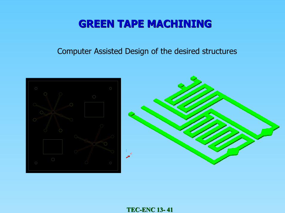
GREEN TAPE MACHININGGREEN TAPE MACHINING
Computer Assisted Design of the desired structures
TECTEC--ENC 13ENC 13-- 4242
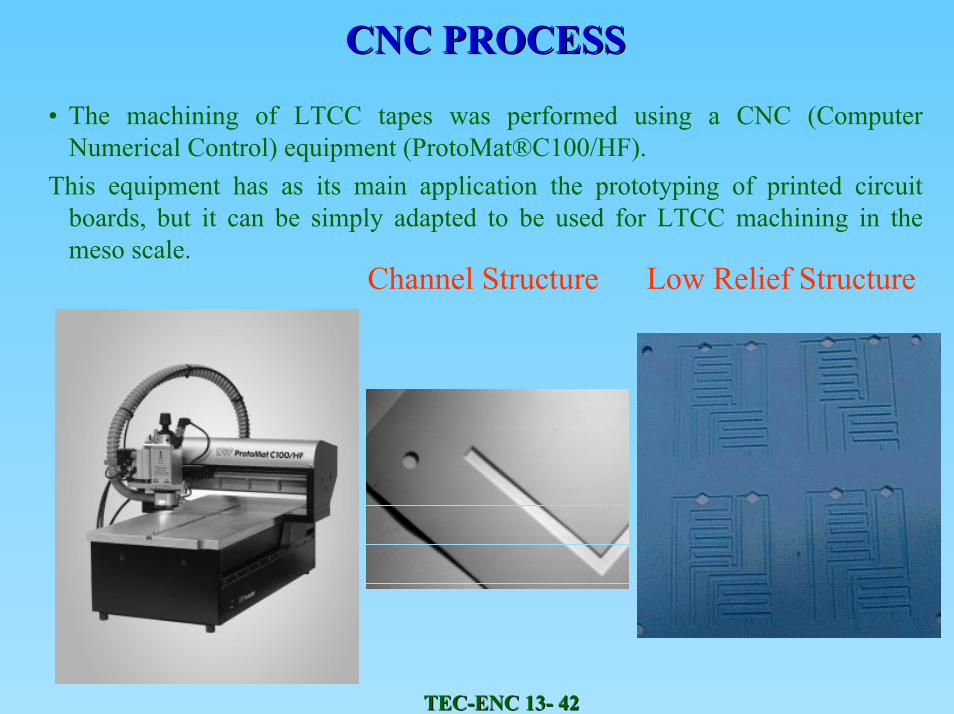
CNC PROCESSCNC PROCESS
• The machining of LTCC tapes was performed using a CNC (Computer Numerical Control) equipment (ProtoMat®C100/HF).
This equipment has as its main application the prototyping of printed circuit boards, but it can be simply adapted to be used for LTCC machining in the meso scale.
Channel Structure Low Relief Structure
TECTEC--ENC 13ENC 13-- 4343
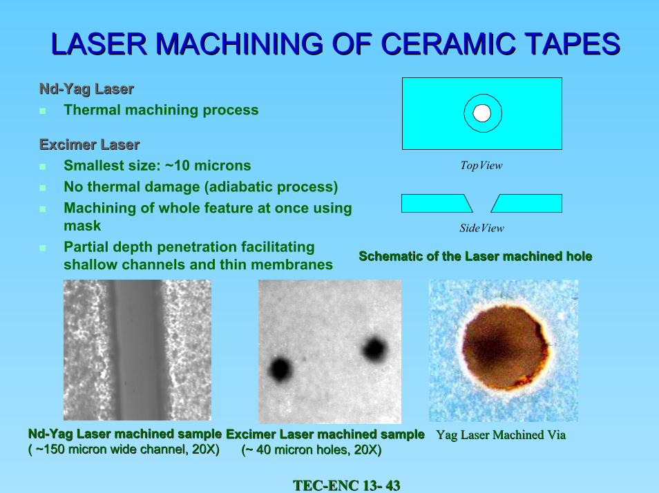
LASER MACHINING OF CERAMIC TAPESLASER MACHINING OF CERAMIC TAPESNdNd--YagYag LaserLaser
Thermal machining process
ExcimerExcimer LaserLaserSmallest size: ~10 micronsNo thermal damage (adiabatic process)Machining of whole feature at once using maskPartial depth penetration facilitating shallow channels and thin membranes Schematic of the Laser machined hole Schematic of the Laser machined hole
SideView
TopView
ExcimerExcimer Laser machined sampleLaser machined sample(~ 40 micron holes, 20X) (~ 40 micron holes, 20X)
NdNd--YagYag Laser machined sampleLaser machined sample( ~150 micron wide channel, 20X)( ~150 micron wide channel, 20X)
Yag Yag Laser Laser Machined Machined ViaVia
TECTEC--ENC 13ENC 13-- 4444
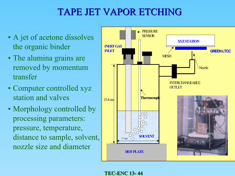
TAPE JET VAPOR ETCHING TAPE JET VAPOR ETCHING
7.7 cm
INERT GAS INLET
INTERCHANGEABLE OUTLET
SOLVENT
XYZ STATION
GREEN LTCC MESH
15.4 cm
HOT PLATE
Thermocouple
PRESSURE SENSOR
Nozzle
• A jet of acetone dissolves the organic binder
• The alumina grains are removed by momentum transfer
• Computer controlled xyz station and valves
• Morphology controlled by processing parameters: pressure, temperature, distance to sample, solvent, nozzle size and diameter

TECTEC--ENC 13ENC 13-- 4545
ADVANTAGES OF JET VAPOR ETCHINGADVANTAGES OF JET VAPOR ETCHING
• Rapid prototypes– More flexible than
traditional punching technique
• One can do partial cavities and continuous borders when machining long channels
– Processing and instrumentation costs are a fraction of conventional punch and die process
Features as small as 10µm has been obtained
TECTEC--ENC 13ENC 13-- 4646
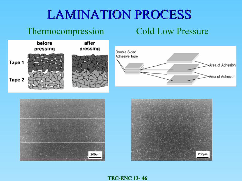
LAMINATION PROCESSLAMINATION PROCESSThermocompression Cold Low Pressure
TECTEC--ENC 13ENC 13-- 4747
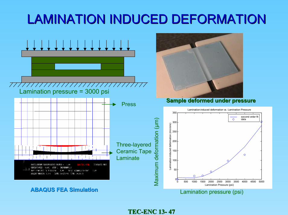
LAMINATION INDUCED DEFORMATIONLAMINATION INDUCED DEFORMATION
ABAQUS FEA SimulationABAQUS FEA Simulation
Press
Three-layeredCeramic TapeLaminate
Lamination pressure = 3000 psi
0 500 1000 1500 2000 2500 3000 3500 4000 4500 50000
50
100
150
200
250
300
350
Lamination Pressure (psi)
Lam
inat
ion-
indu
ced
defo
rmat
ion
(mic
rons
)
Lamination-induced deformation vs. Lamination Pressure
second order fitdata
Lamination pressure (psi)
Sample deformed under pressureSample deformed under pressure
Max
imum
def
orm
atio
n (µ
m)
TECTEC--ENC 13ENC 13-- 4848
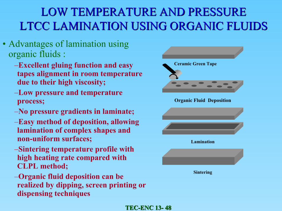
LOW TEMPERATURE AND PRESSURE LOW TEMPERATURE AND PRESSURE LTCC LAMINATION USING ORGANIC FLUIDSLTCC LAMINATION USING ORGANIC FLUIDS
• Advantages of lamination using organic fluids :
–Excellent gluing function and easytapes alignment in room temperature due to their high viscosity;
–Low pressure and temperature process;
–No pressure gradients in laminate;–Easy method of deposition, allowing lamination of complex shapes and non-uniform surfaces;
–Sintering temperature profile with high heating rate compared withCLPL method;
–Organic fluid deposition can be realized by dipping, screen printing or dispensing techniques
Ceramic Green Tape
Lamination
Sintering
Organic Fluid Deposition
TECTEC--ENC 13ENC 13-- 4949
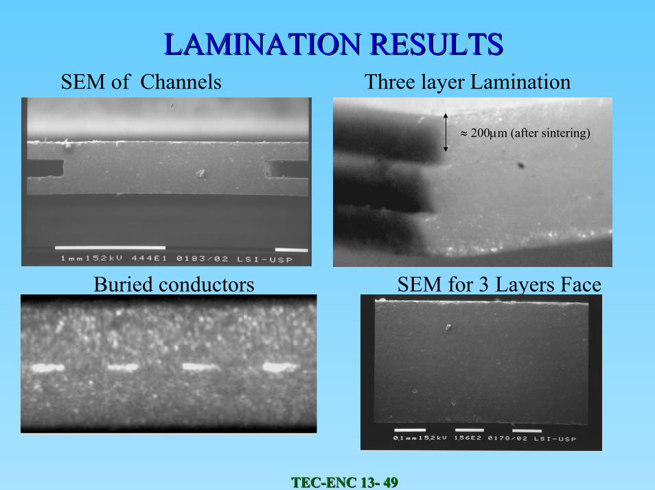
LAMINATION RESULTSLAMINATION RESULTSSEM of Channels Three layer Lamination
≈ 200µm (after sintering)
Buried conductors SEM for 3 Layers Face
TECTEC--ENC 13ENC 13-- 5050
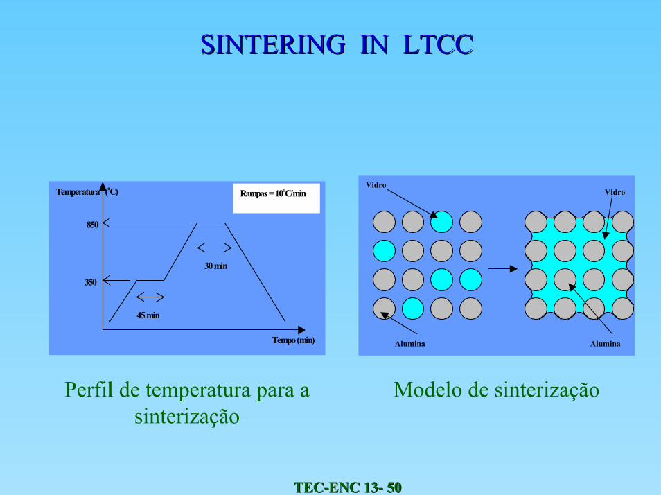
SINTERING IN LTCCSINTERING IN LTCC
Vidro
Alumina
Vidro
Alumina
850
350
Temperatura (oC)
Tempo (min)
45 min
30 min
Rampas = 10oC/min
Perfil de temperatura para a sinterização
Modelo de sinterização
TECTEC--ENC 13ENC 13-- 5151
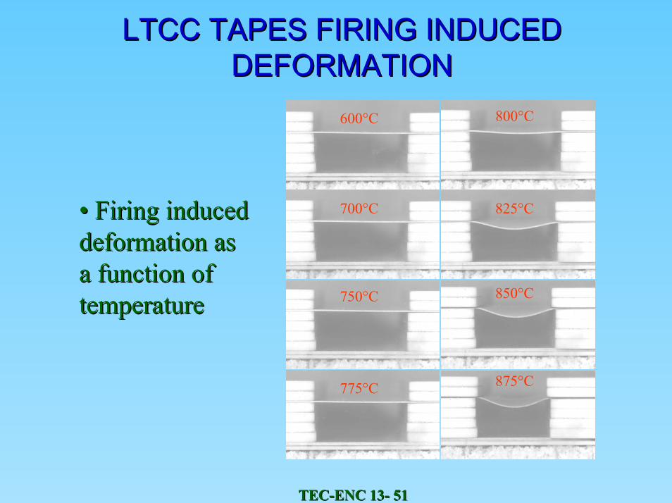
LTCC TAPES FIRING INDUCED LTCC TAPES FIRING INDUCED DEFORMATIONDEFORMATION
600°C 800°C
•• Firing induced Firing induced deformation as deformation as a function of a function of temperature
700°C 825°C
750°C 850°Ctemperature
775°C 875°C
TECTEC--ENC 13ENC 13-- 5252
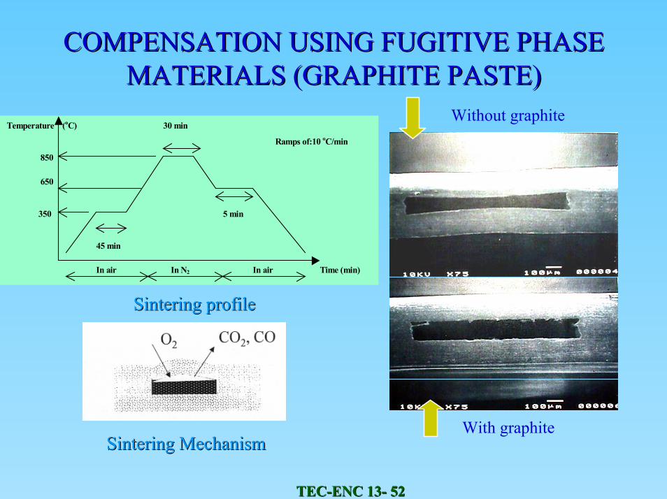
COMPENSATION USING FUGITIVE PHASE COMPENSATION USING FUGITIVE PHASE MATERIALS (GRAPHITE PASTE)MATERIALS (GRAPHITE PASTE)
Without graphite
With graphite
Sintering profile Sintering profile
850
350
Temperature (oC)
Time (min)
45 min
30 min
650
In air In N2 In air
5 min
Ramps of:10 oC/min
Sintering MechanismSintering Mechanism
TECTEC--ENC 13ENC 13-- 5353
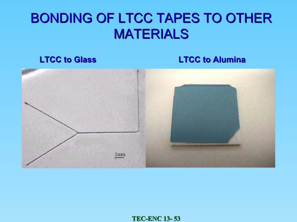
BONDING OF LTCC TAPES TO OTHER BONDING OF LTCC TAPES TO OTHER MATERIALSMATERIALS
LTCC to LTCC to AluminaAluminaLTCC to GlassLTCC to Glass
TECTEC--ENC 13ENC 13-- 5454
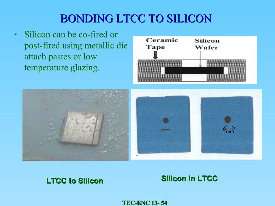
BONDING LTCC TO SILICONBONDING LTCC TO SILICON• Silicon can be co-fired or
post-fired using metallic die attach pastes or low temperature glazing.
2 mm
SiliconSilicon in LTCCin LTCCLTCC to SiliconLTCC to Silicon
TECTEC--ENC 13ENC 13-- 5555
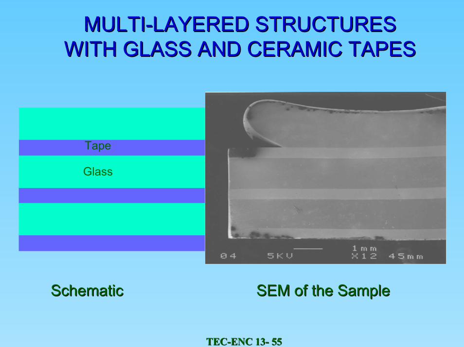
MULTIMULTI--LAYERED STRUCTURESLAYERED STRUCTURESWITH GLASS AND CERAMIC TAPESWITH GLASS AND CERAMIC TAPES
Tape
Glass
SchematicSchematic SEM of the SampleSEM of the Sample
TECTEC--ENC 13ENC 13-- 5656
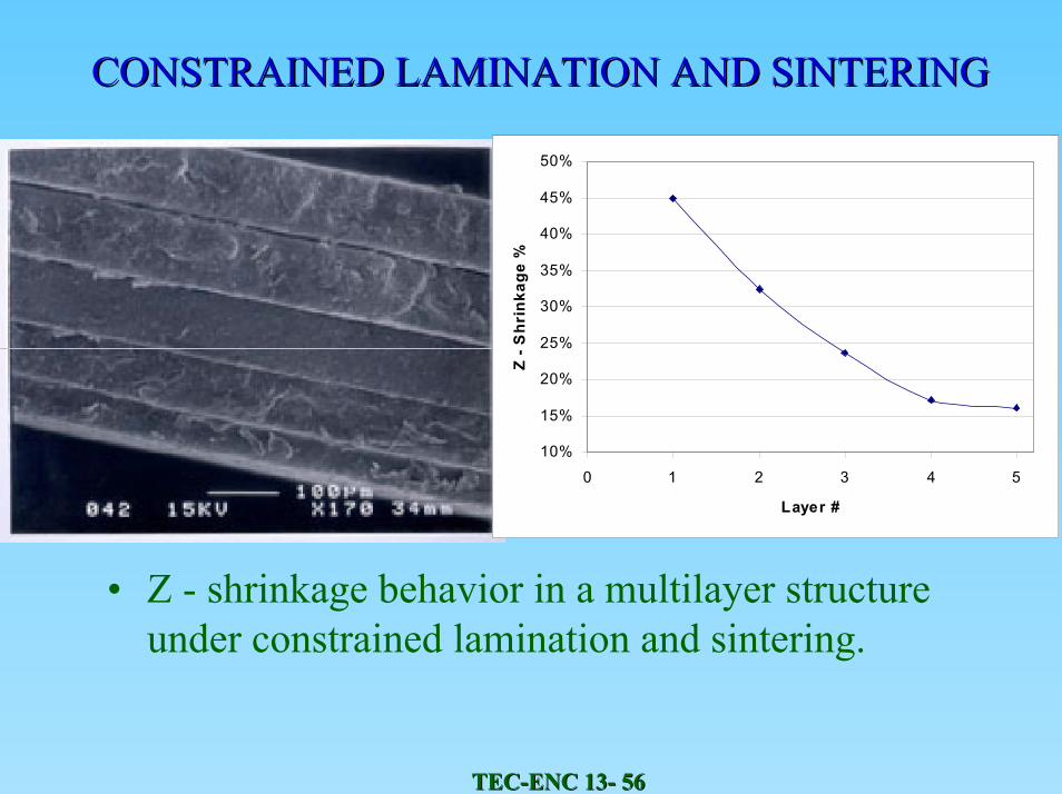
CONSTRAINED LAMINATION AND SINTERINGCONSTRAINED LAMINATION AND SINTERING
10%
15%
20%
25%
30%
35%
40%
45%
50%
0 1 2 3 4 5
Layer #Z
- Shr
inka
ge %
• Z - shrinkage behavior in a multilayer structure under constrained lamination and sintering.
TECTEC--ENC 13ENC 13-- 5757
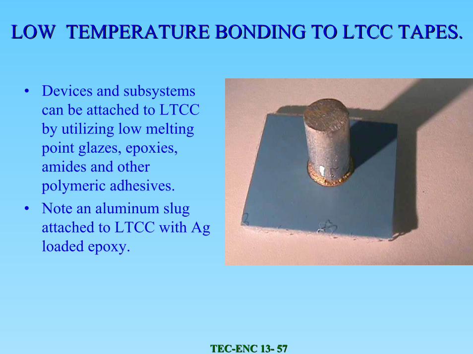
LOW TEMPERATURE BONDING TO LTCC TAPES.LOW TEMPERATURE BONDING TO LTCC TAPES.
• Devices and subsystems can be attached to LTCC by utilizing low melting point glazes, epoxies, amides and other polymeric adhesives.
• Note an aluminum slug attached to LTCC with Ag loaded epoxy.
TECTEC--ENC 13ENC 13-- 5858
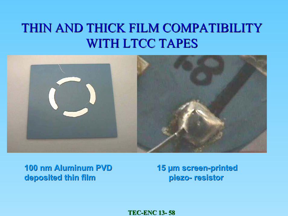
THIN AND THICK FILM COMPATIBILITYTHIN AND THICK FILM COMPATIBILITYWITH LTCC TAPESWITH LTCC TAPES
100 nm Aluminum PVD 100 nm Aluminum PVD deposited thin filmdeposited thin film
15 µm screen15 µm screen--printed printed piezopiezo-- resistor resistor

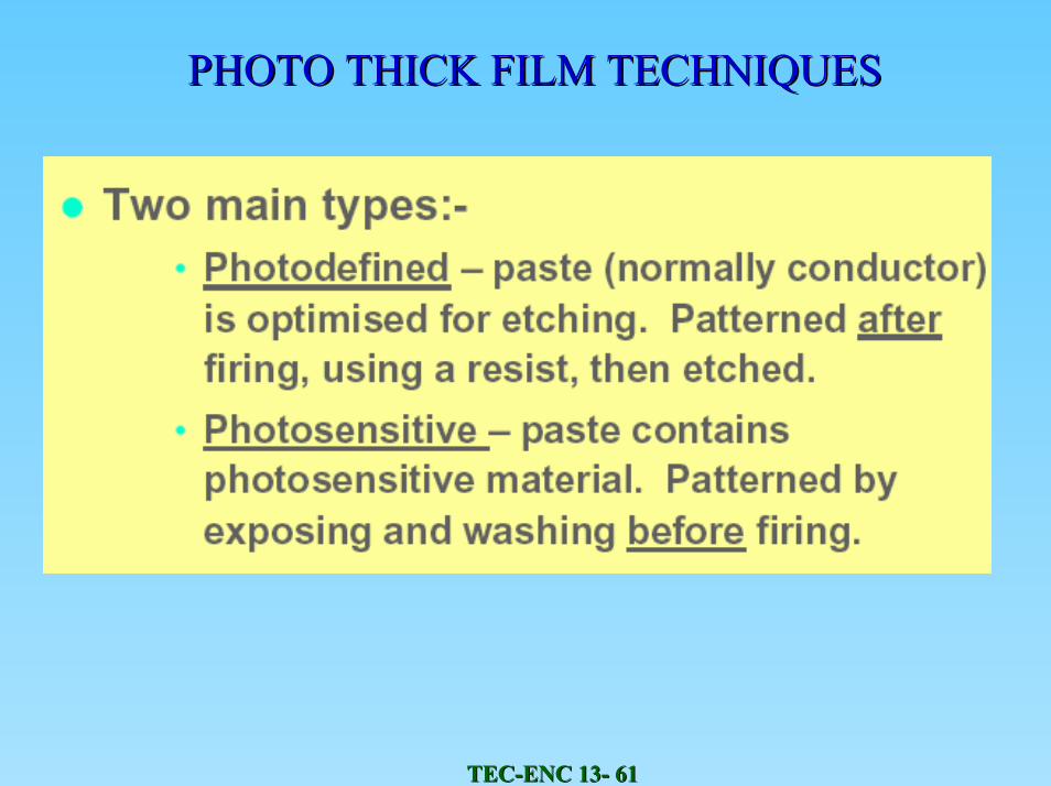
PHOTO PATTERNED THICK FILM PROCESSESPHOTO PATTERNED THICK FILM PROCESSES
• Photo Defined Thick FilmPhoto Defined Thick Film••Photo Sensitive Thick FilmPhoto Sensitive Thick Film•• Fodel Fodel CompositionsCompositions•• Diffusion PatterningDiffusion Patterning
TECTEC--ENC 13ENC 13-- 6060
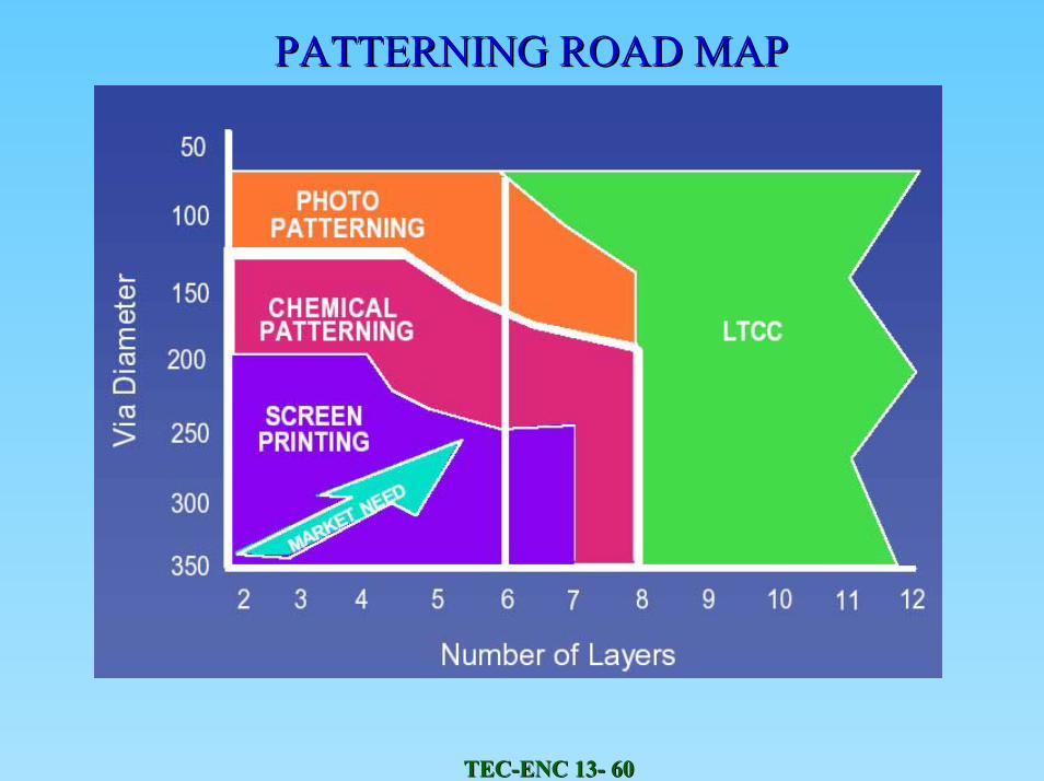
PATTERNING ROAD MAPPATTERNING ROAD MAP
TECTEC--ENC 13ENC 13-- 6161
PHOTO THICK FILM TECHNIQUESPHOTO THICK FILM TECHNIQUES
TECTEC--ENC 13ENC 13-- 6262
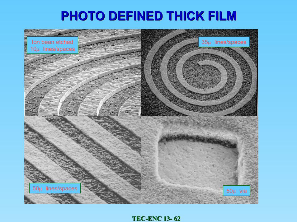
PHOTO DEFINED THICK FILMPHOTO DEFINED THICK FILM
Ion bean etched10µ lines/spaces
50µ lines/spaces
35µ lines/spaces
50µ via
TECTEC--ENC 13ENC 13-- 6363
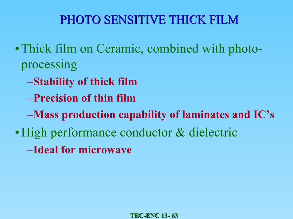
PHOTO SENSITIVE THICK FILMPHOTO SENSITIVE THICK FILM
• Thick film on Ceramic, combined with photo-processing
–Stability of thick film–Precision of thin film–Mass production capability of laminates and IC’s
• High performance conductor & dielectric –Ideal for microwave
TECTEC--ENC 13ENC 13-- 6464
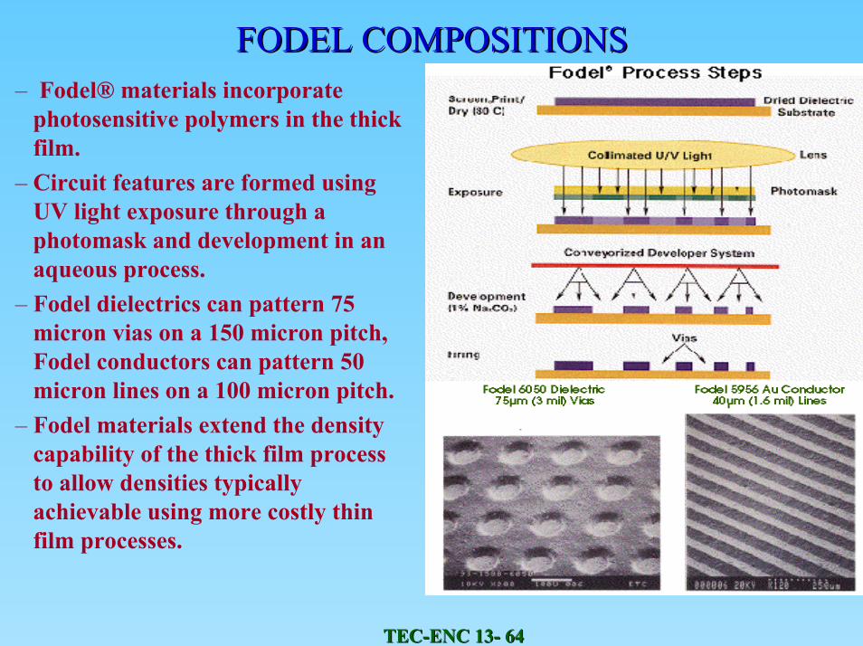
FODEL COMPOSITIONSFODEL COMPOSITIONS– Fodel® materials incorporate
photosensitive polymers in the thick film.
– Circuit features are formed using UV light exposure through a photomask and development in an aqueous process.
– Fodel dielectrics can pattern 75 micron vias on a 150 micron pitch, Fodel conductors can pattern 50 micron lines on a 100 micron pitch.
– Fodel materials extend the density capability of the thick film process to allow densities typically achievable using more costly thin film processes.
TECTEC--ENC 13ENC 13-- 6565
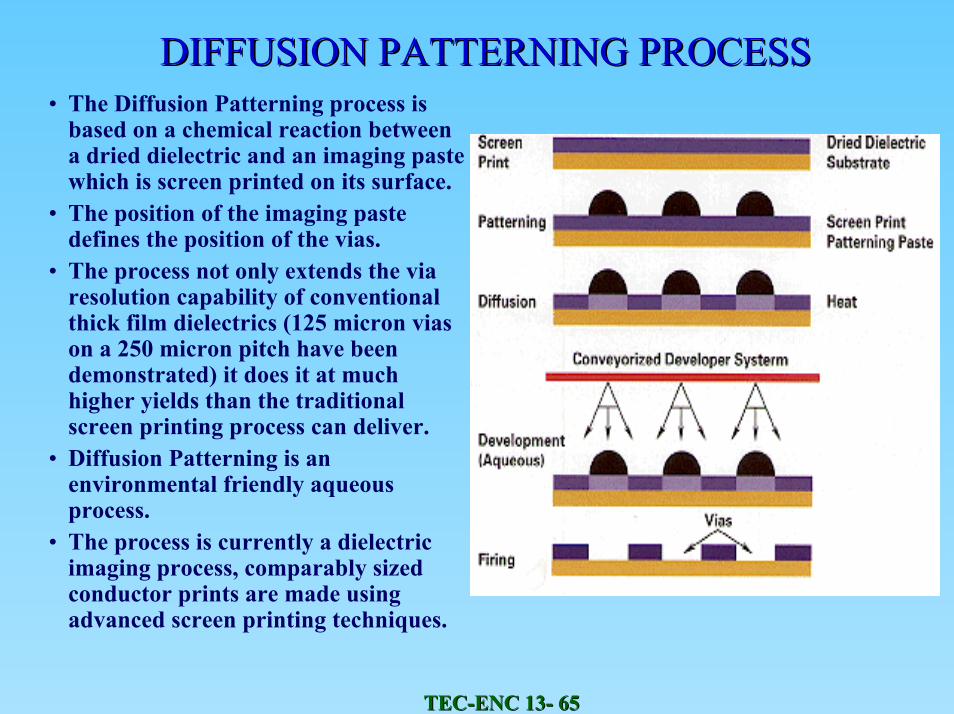
DIFFUSION PATTERNING PROCESS DIFFUSION PATTERNING PROCESS • The Diffusion Patterning process is
based on a chemical reaction between a dried dielectric and an imaging paste which is screen printed on its surface.
• The position of the imaging paste defines the position of the vias.
• The process not only extends the via resolution capability of conventional thick film dielectrics (125 micron viason a 250 micron pitch have been demonstrated) it does it at much higher yields than the traditional screen printing process can deliver.
• Diffusion Patterning is an environmental friendly aqueous process.
• The process is currently a dielectric imaging process, comparably sized conductor prints are made using advanced screen printing techniques.
TECTEC--ENC 13ENC 13-- 6666
NEW LTCC TAPE SYSTEMSNEW LTCC TAPE SYSTEMS
–– Zero Shrinkage LTCC TapesZero Shrinkage LTCC Tapes–– LTCC on Metal (LTCCLTCC on Metal (LTCC--M)M)–– Transfer LTCC tape (LTCCTransfer LTCC tape (LTCC--C)C)–– Photo Photo ImageableImageable LTCC (PILTCC (PI--LTCC)LTCC)
TECTEC--ENC 13ENC 13-- 6767
ZERO SHRINKAGE LTCC TAPES ZERO SHRINKAGE LTCC TAPES – Recent developments relating to the formulation, processing and manufacturing of
ceramic and glass composites, which do not shrink upon co-firing to the degree of ordinary LTCC materials, a slight shrinkage (< 2%) can be controlled to a very tight tolerance of +/- 0.01%.
– Because ZR tapes exhibits a near zero shrinkage and zero shrinkage tolerance upon firing, precise feature locations are maintained in the X, Y, and Z axis's and yield improvements of over 30% can be realized when compared to conventional materials systems.
– Some properties include the embedding and co-firing of: discrete components such as ceramic chip capacitors for true passive integration, ceramic heatspreaders with integral heat pipes for thermal management (>2000 W/mK)
– The main difference between Zero Shrinkage tapes and all other LTCC tapes is its unique shrinkage properties during firing.
– Free sintered this tapes densifies by shrinking in the z-axis.– Key Benefits are:
• Near zero (<0.2% ± 0.05%) x-y shrinkage with no added processing steps• Compatible with co-fired solderable conductors• Cavity structures cut into the green tape show no x-y shrinkage or distortion after firing• Lead and cadmium free• High Q
TECTEC--ENC 13ENC 13-- 6868
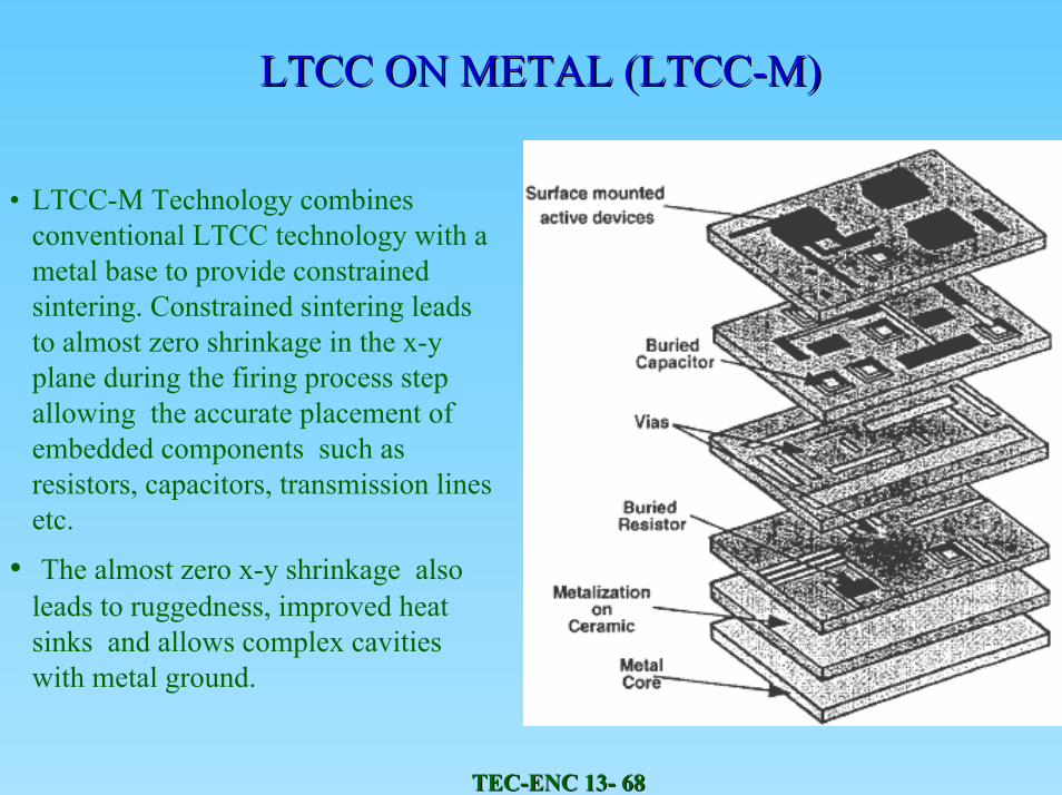
LTCC ON METAL (LTCCLTCC ON METAL (LTCC--M)M)
• LTCC-M Technology combines conventional LTCC technology with a metal base to provide constrained sintering. Constrained sintering leads to almost zero shrinkage in the x-y plane during the firing process step allowing the accurate placement of embedded components such as resistors, capacitors, transmission lines etc.
• The almost zero x-y shrinkage also leads to ruggedness, improved heat sinks and allows complex cavities with metal ground.
TECTEC--ENC 13ENC 13-- 6969
TRANSFER TAPE (LTCCTRANSFER TAPE (LTCC--C)C)• A low Dielectric Constant Tape for Use with 96% Alumina Substrates. A
flexible cast film of inorganic dielectric powder dispersed in an organic matrix, designed to be laminated to and fired on an Alumina substrate. A pressure/temperature combination of 1.7-6.9 MPa and 70°C works well for laminating this tape.
• After lamination, the parts can be fired in a belt furnace at 580°C peak/50 minute cycle burnout followed by an 850°C peak/45 minute cycle for sintering, rendering a fired Shrinkage of : zero to X and Y axis and 45%-55% in Z axis.
• Multilayer parts can be formed by metallizing laminated and fired sheets progressively. This tape is useful when low dielectric constant and low loss are desired.
• Lo-Fire tape is provided on a silicone-coated polyester film to minimize environmental contamination, to protect it from mechanical damage, and to aid in handling.
TECTEC--ENC 13ENC 13-- 7070
PHOTO IMAGEABLE LTCC (PIPHOTO IMAGEABLE LTCC (PI--LTCC)LTCC)
• The PI-LTCC consists of a mixture of photo-polymer organics and ceramic / glass powders doctor bladed onto a 3 mils Mylar film.
• The Photo Imageable LTCC tape offers the advantage of economy by fast and efficient processing combined with the convenience of having an LTCC system very similar in properties to the conventional compositions.
TECTEC--ENC 13ENC 13-- 7171
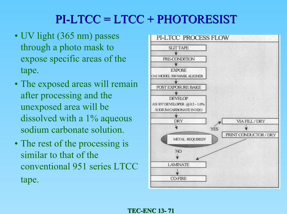
PIPI--LTCC = LTCC + PHOTORESISTLTCC = LTCC + PHOTORESIST• UV light (365 nm) passes
through a photo mask to expose specific areas of the tape.
• The exposed areas will remain after processing and the unexposed area will be dissolved with a 1% aqueous sodium carbonate solution.
• The rest of the processing is similar to that of the conventional 951 series LTCC tape.
TECTEC--ENC 13ENC 13-- 7272
VIAS IN PIVIAS IN PI--LTCCLTCC
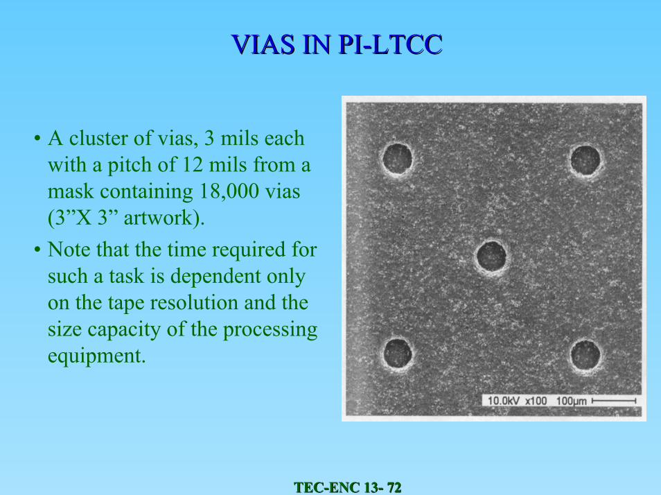
• A cluster of vias, 3 mils each with a pitch of 12 mils from a mask containing 18,000 vias(3”X 3” artwork).
• Note that the time required for such a task is dependent only on the tape resolution and the size capacity of the processing equipment.
TECTEC--ENC 13ENC 13-- 7373
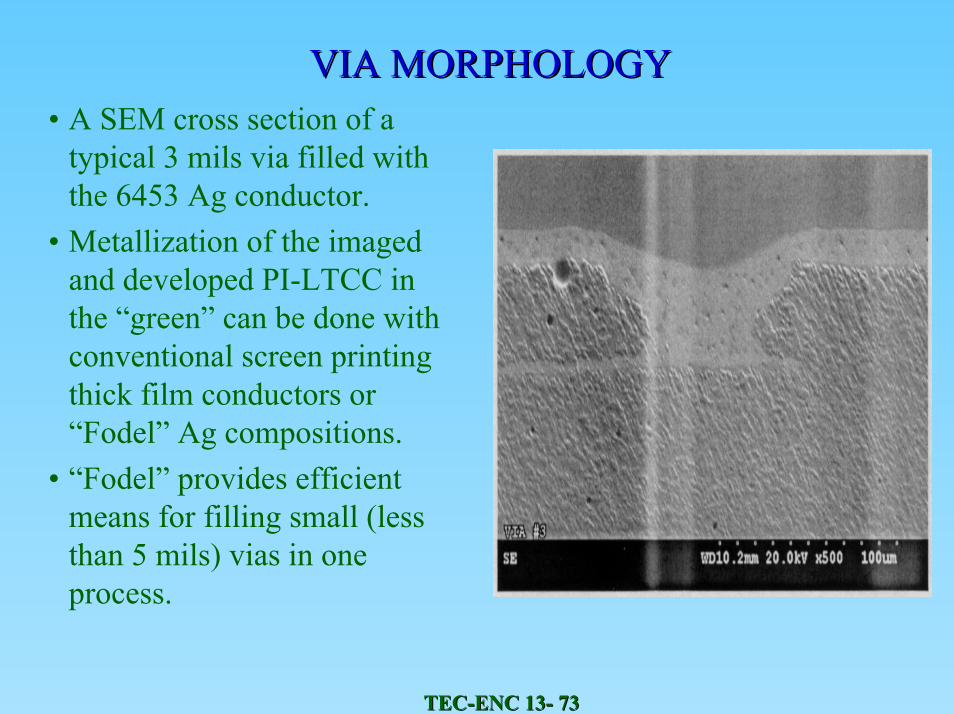
VIA MORVIA MORPHPHOLOGYOLOGY• A SEM cross section of a
typical 3 mils via filled with the 6453 Ag conductor.
• Metallization of the imaged and developed PI-LTCC in the “green” can be done with conventional screen printing thick film conductors or “Fodel” Ag compositions.
• “Fodel” provides efficient means for filling small (less than 5 mils) vias in one process.
TECTEC--ENC 13ENC 13-- 7474
PROCESS TIME TO FORM VIASPROCESS TIME TO FORM VIAS
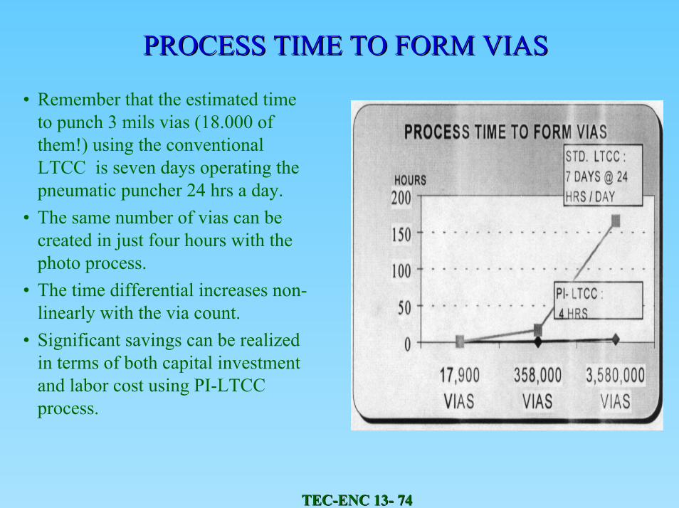
• Remember that the estimated time to punch 3 mils vias (18.000 of them!) using the conventional LTCC is seven days operating the pneumatic puncher 24 hrs a day.
• The same number of vias can be created in just four hours with the photo process.
• The time differential increases non-linearly with the via count.
• Significant savings can be realized in terms of both capital investment and labor cost using PI-LTCC process.
TECTEC--ENC 13ENC 13-- 7575
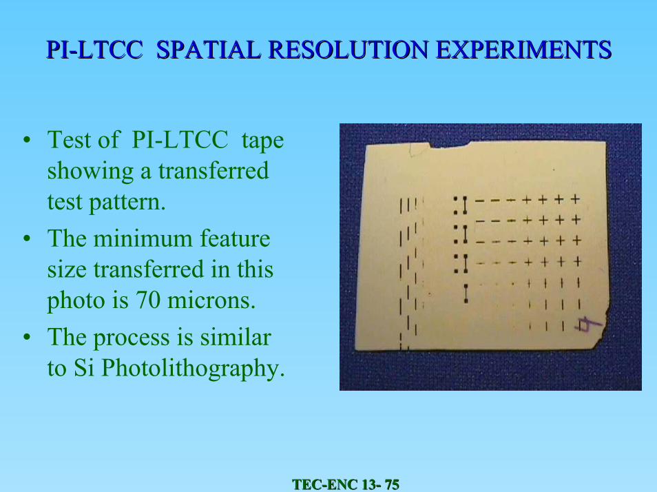
PIPI--LTCC SPATIAL RESOLUTION EXPERIMENTSLTCC SPATIAL RESOLUTION EXPERIMENTS
• Test of PI-LTCC tape showing a transferred test pattern.
• The minimum feature size transferred in this photo is 70 microns.
• The process is similar to Si Photolithography.
TECTEC--ENC 13ENC 13-- 7676
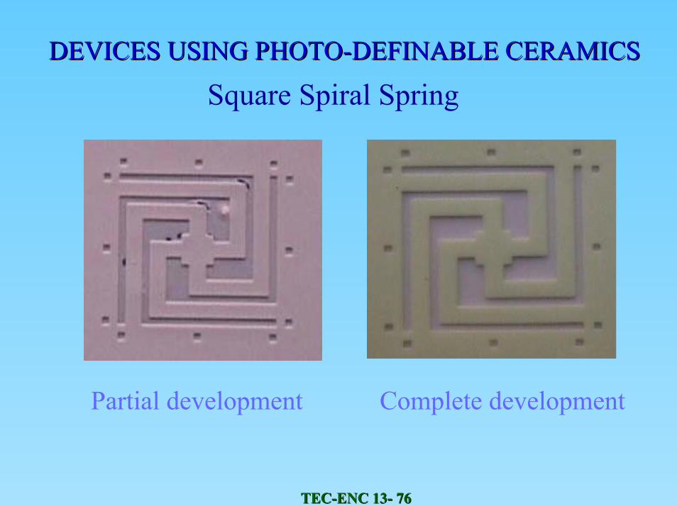
DEVICES USING PHOTODEVICES USING PHOTO--DEFINABLE CERAMICSDEFINABLE CERAMICS
Square Spiral Spring
Complete developmentPartial development
TECTEC--ENC 13ENC 13-- 7777
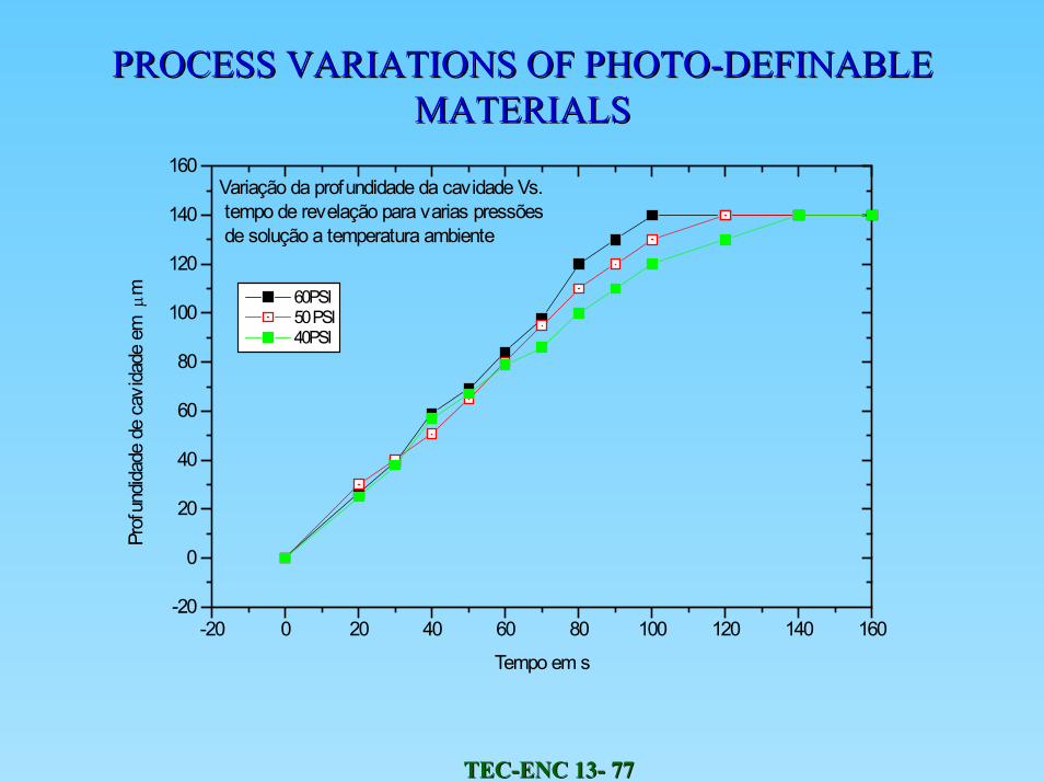
PROCESS VARIATIONS OF PHOTOPROCESS VARIATIONS OF PHOTO--DEFINABLE DEFINABLE MATERIALSMATERIALS
-20 0 20 40 60 80 100 120 140 160-20
0
20
40
60
80
100
120
140
160Variação da profundidade da cavidade Vs. tempo de revelação para varias pressões de solução a temperatura ambiente
60PSI 50 PSI 40PSI
Prof
undid
ade
de c
avida
de e
m µ
m
Tempo em s
TECTEC--ENC 13ENC 13-- 7878
SSAGGING IN EMBEDDED CHANNELSAGGING IN EMBEDDED CHANNELS
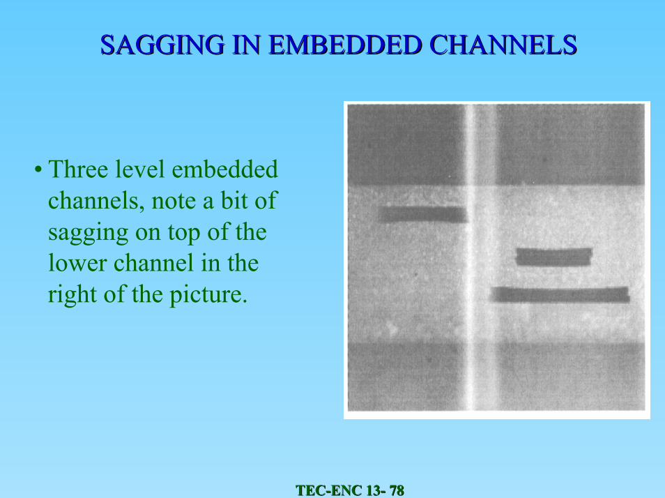
• Three level embedded channels, note a bit of sagging on top of the lower channel in the right of the picture.
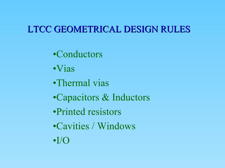
LTCC GEOMETRICAL DESIGN RULESLTCC GEOMETRICAL DESIGN RULES
•Conductors•Vias•Thermal vias•Capacitors & Inductors•Printed resistors•Cavities / Windows•I/O
TECTEC--ENC 13ENC 13-- 8080
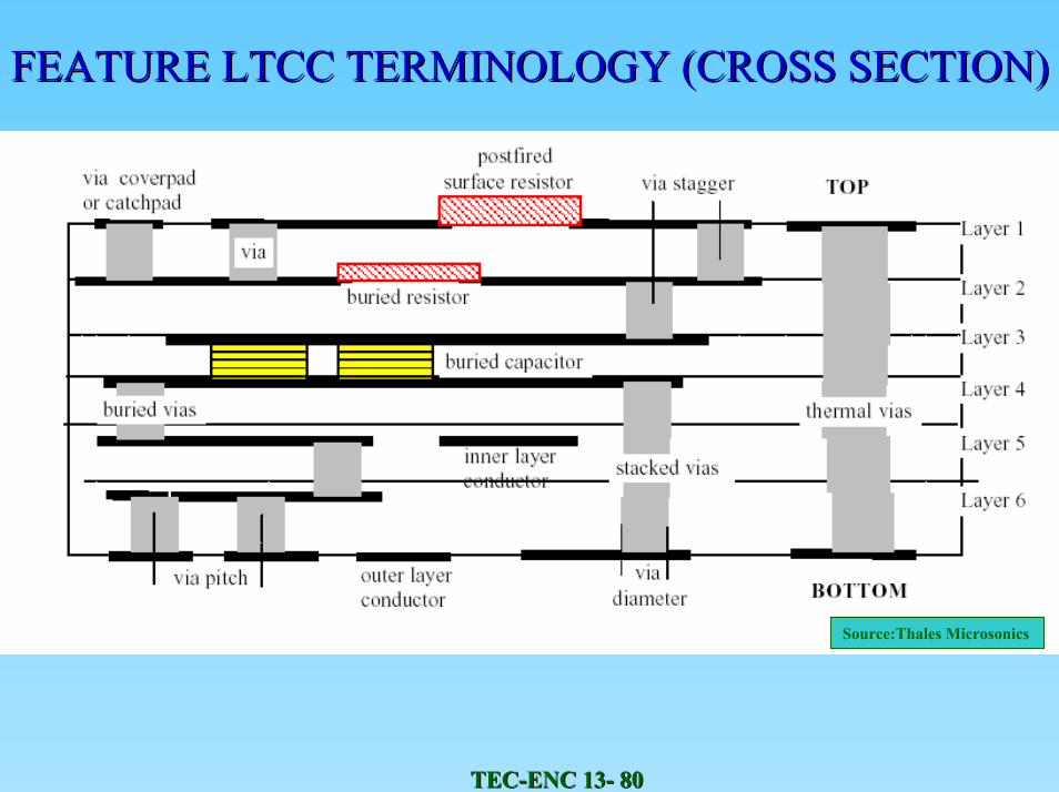
FEATURE LTCC TERMINOLOGY (CROSS SECTION) FEATURE LTCC TERMINOLOGY (CROSS SECTION)
Source:Thales Microsonics
TECTEC--ENC 13ENC 13-- 8181
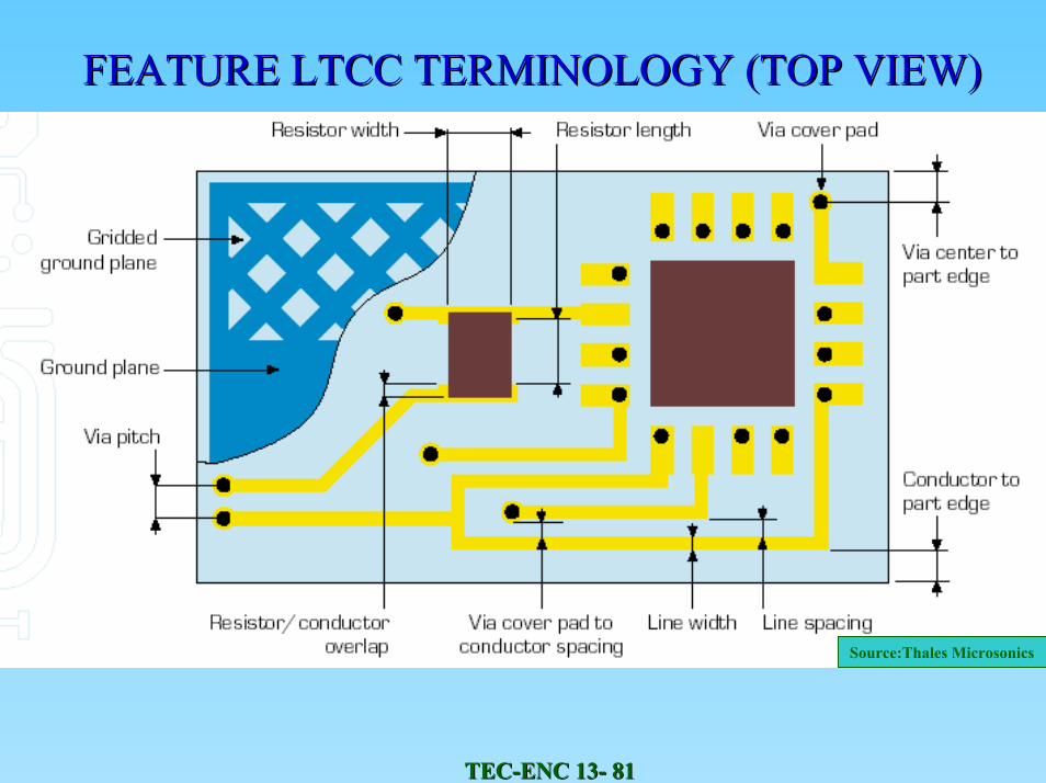
FEATURE LTCC TERMINOLOGY (TOP VIEW)FEATURE LTCC TERMINOLOGY (TOP VIEW)
Source:Thales Microsonics
TECTEC--ENC 13ENC 13-- 8282
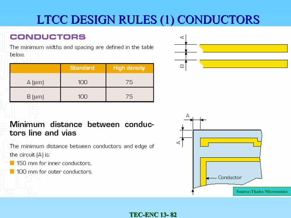
LTCC DESIGN RULES (1) CONDUCTORSLTCC DESIGN RULES (1) CONDUCTORS
Source:Thales Microsonics
TECTEC--ENC 13ENC 13-- 8383
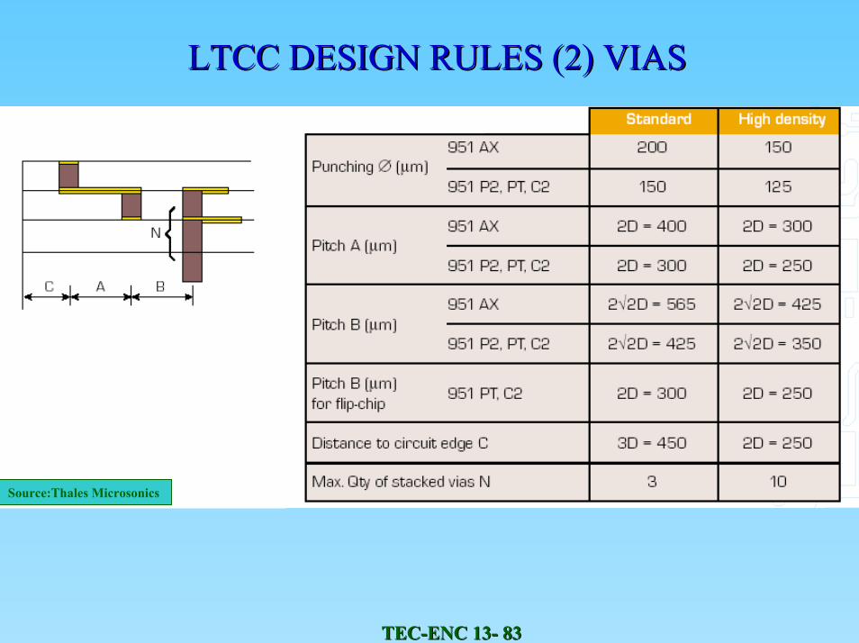
LTCC DESIGN RULES (2) VIASLTCC DESIGN RULES (2) VIAS
Source:Thales Microsonics
TECTEC--ENC 13ENC 13-- 8484
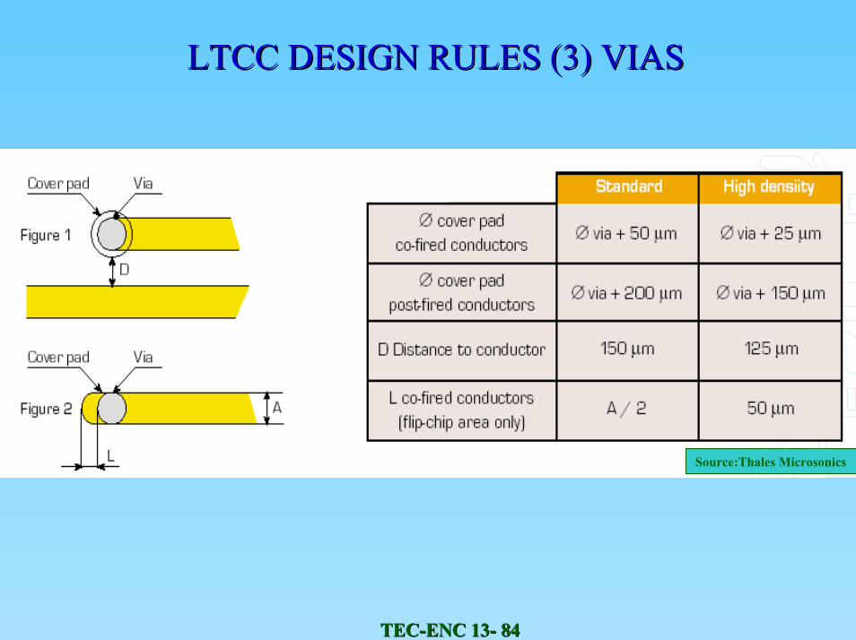
LTCC DESIGN RULES (3) VIASLTCC DESIGN RULES (3) VIAS
Source:Thales Microsonics
TECTEC--ENC 13ENC 13-- 8585
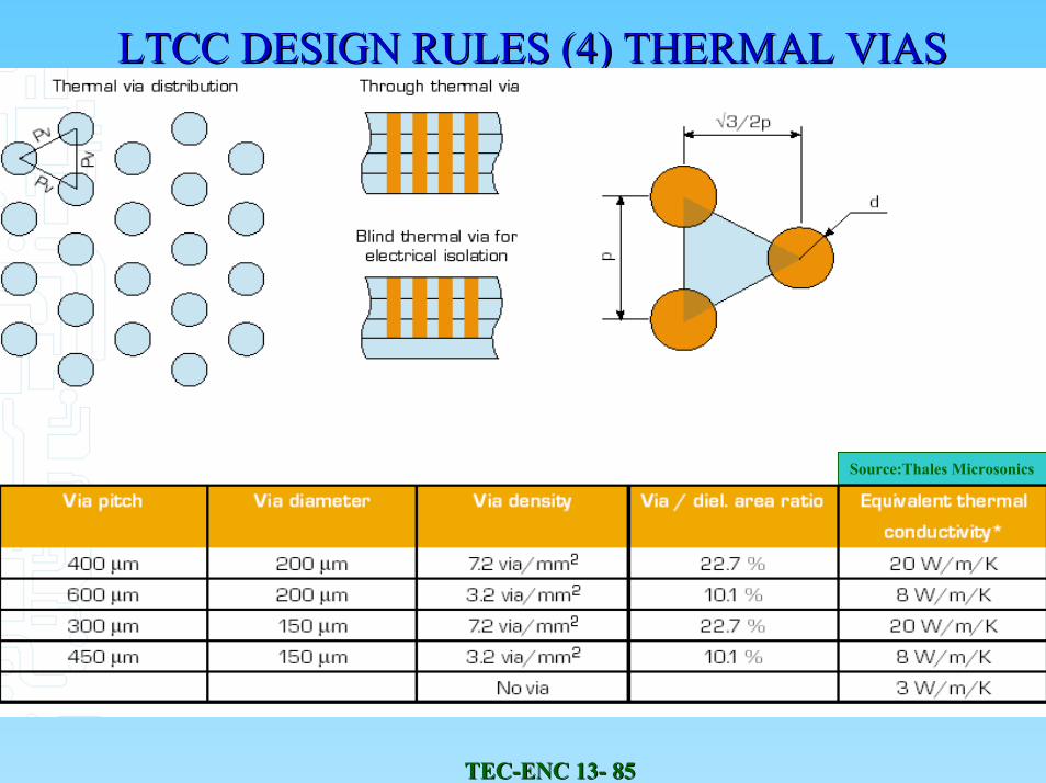
LTCC DESIGN RULES (4) THERMAL VIASLTCC DESIGN RULES (4) THERMAL VIAS
Source:Thales Microsonics
TECTEC--ENC 13ENC 13-- 8686
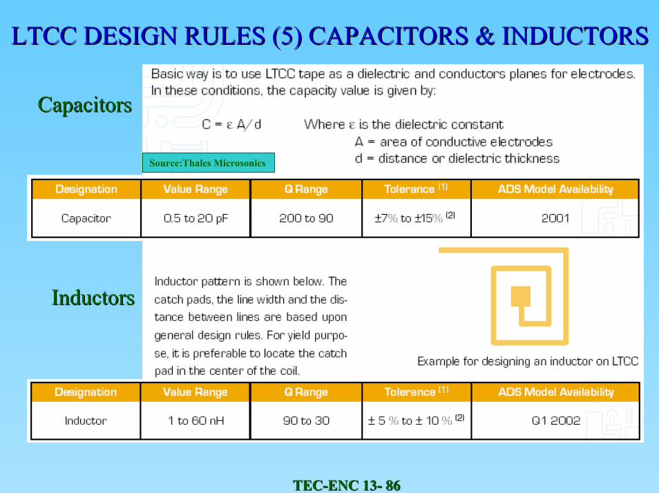
LTCC DESIGN RULES (5) CAPACITORS & INDUCTORSLTCC DESIGN RULES (5) CAPACITORS & INDUCTORS
CapacitorsCapacitors
InductorsInductors
Source:Thales Microsonics
TECTEC--ENC 13ENC 13-- 8787
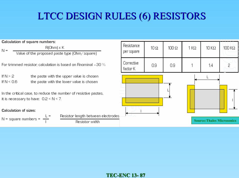
LTCC DESIGN RULES (6) RESISTORSLTCC DESIGN RULES (6) RESISTORS
Source:Thales Microsonics
TECTEC--ENC 13ENC 13-- 8888
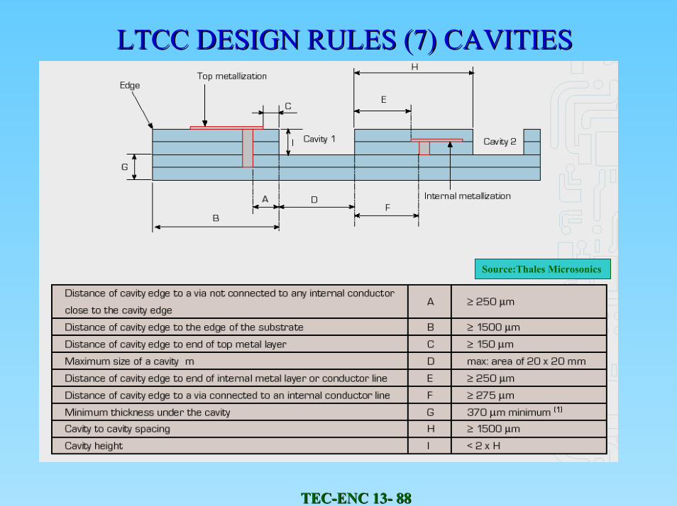
LTCC DESIGN RULES (7) CAVITIESLTCC DESIGN RULES (7) CAVITIES
Source:Thales Microsonics
TECTEC--ENC 13ENC 13-- 8989
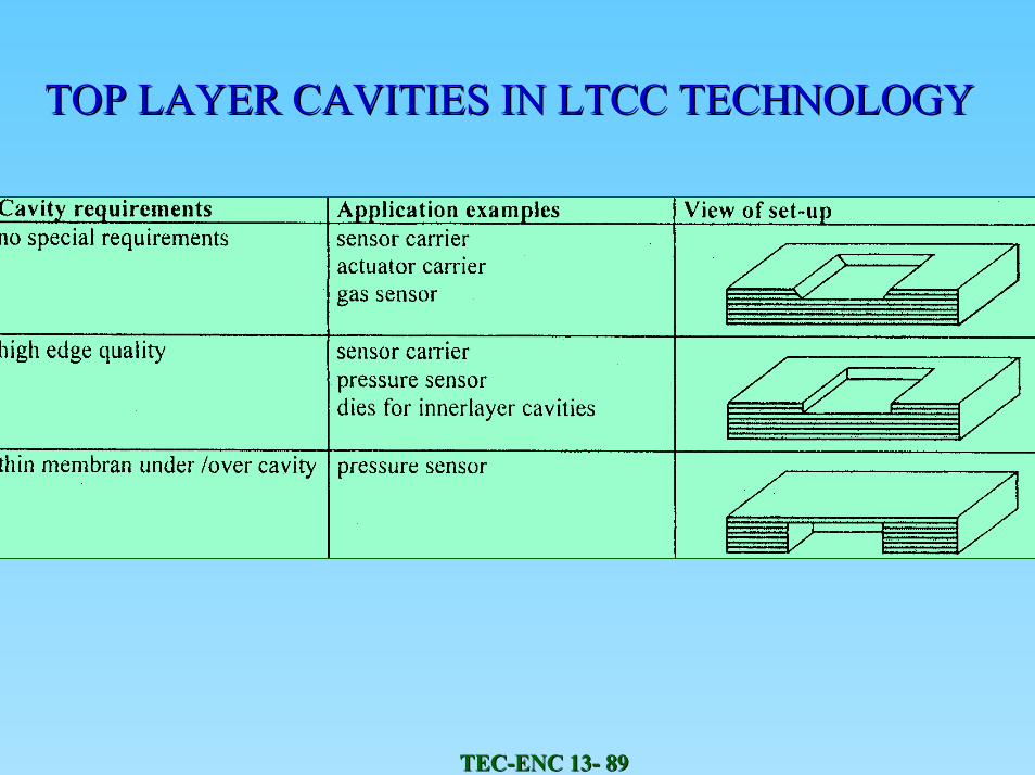
TOP LAYER CAVITIES IN LTCC TECHNOLOGY TOP LAYER CAVITIES IN LTCC TECHNOLOGY
TECTEC--ENC 13ENC 13-- 9090
INNER LAYER CAVITIES IN LTCC TECHNOLOGY INNER LAYER CAVITIES IN LTCC TECHNOLOGY
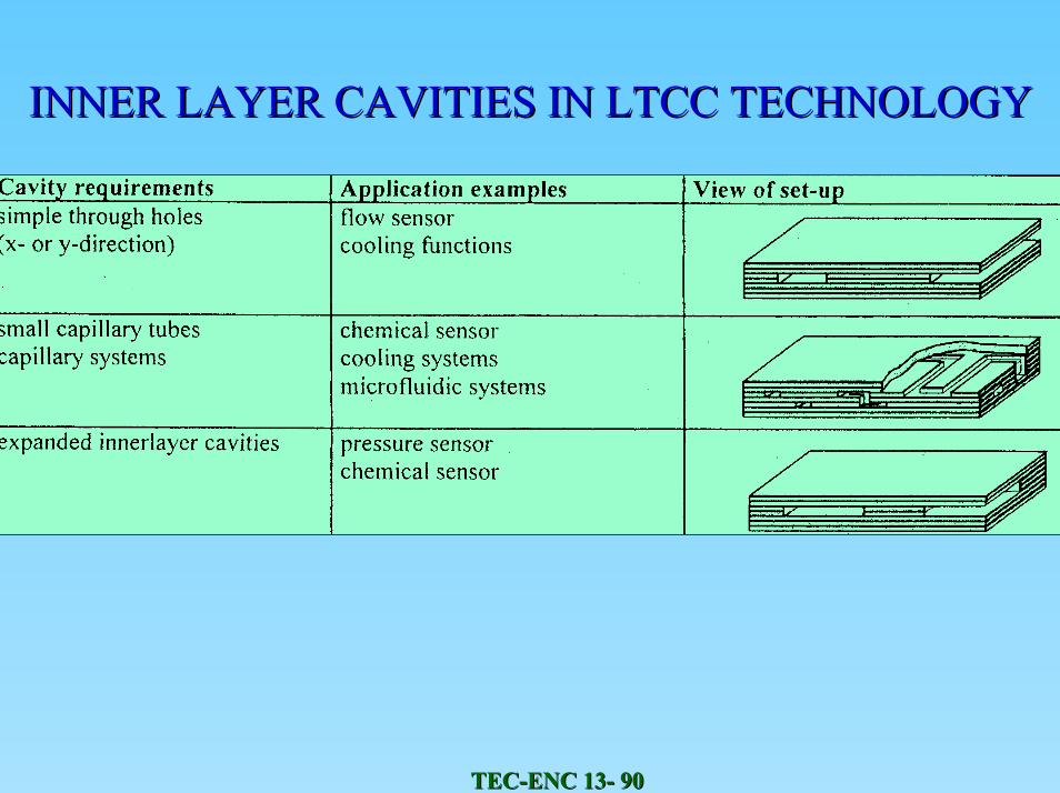
TECTEC--ENC 13ENC 13-- 9191
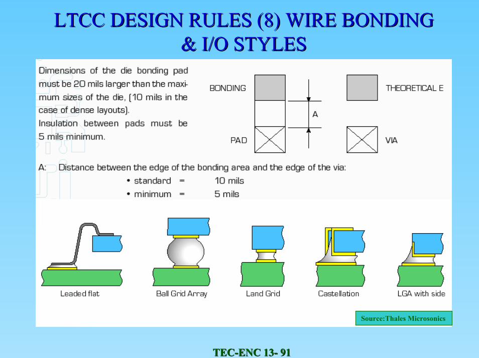
LTCC DESIGN RULES (8) WIRE BONDING LTCC DESIGN RULES (8) WIRE BONDING & I/O STYLES& I/O STYLES
Source:Thales Microsonics
TECTEC--ENC 13ENC 13-- 9292
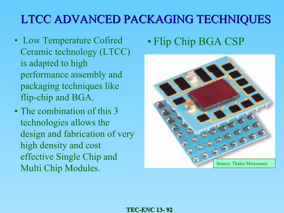
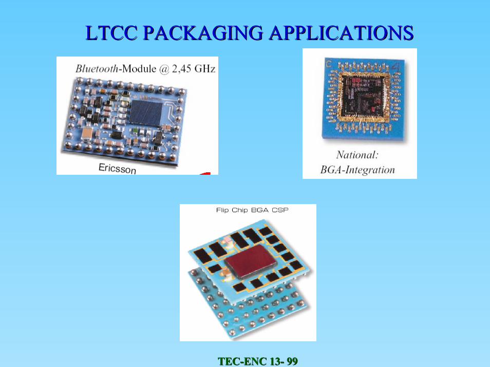
LTCC LTCC ADVANCED PACKAGING TECHNIQUESADVANCED PACKAGING TECHNIQUES
• Low Temperature CofiredCeramic technology (LTCC) is adapted to high performance assembly and packaging techniques like flip-chip and BGA.
• The combination of this 3 technologies allows thedesign and fabrication of very high density and costeffective Single Chip and Multi Chip Modules.
• Flip Chip BGA CSP
Source: Thales Microsonic
TECTEC--ENC 13ENC 13-- 9393
FLIPFLIP--CHIP ON LTCCCHIP ON LTCC
• Characteristics of flip-chip on LTCC
–Peripheral and area I/O pad distribution
– I/O pitch down to 250 µm (125 µm bump)
–3 possible bonding techniques
• SnPb solder reflow• thermocompression• conductive adhesive
• Advantages of flip-chip on LTCC
–Direct bonding on top vias (no additional metallization required)
–LTCC CTE very close to silicon CTE
–High routing capability of the LTCC technology thanks to:
• buried via structures (diameter down to 100 µm)
• line pitch down to 200 µm• high number of layers
TECTEC--ENC 13ENC 13-- 9494
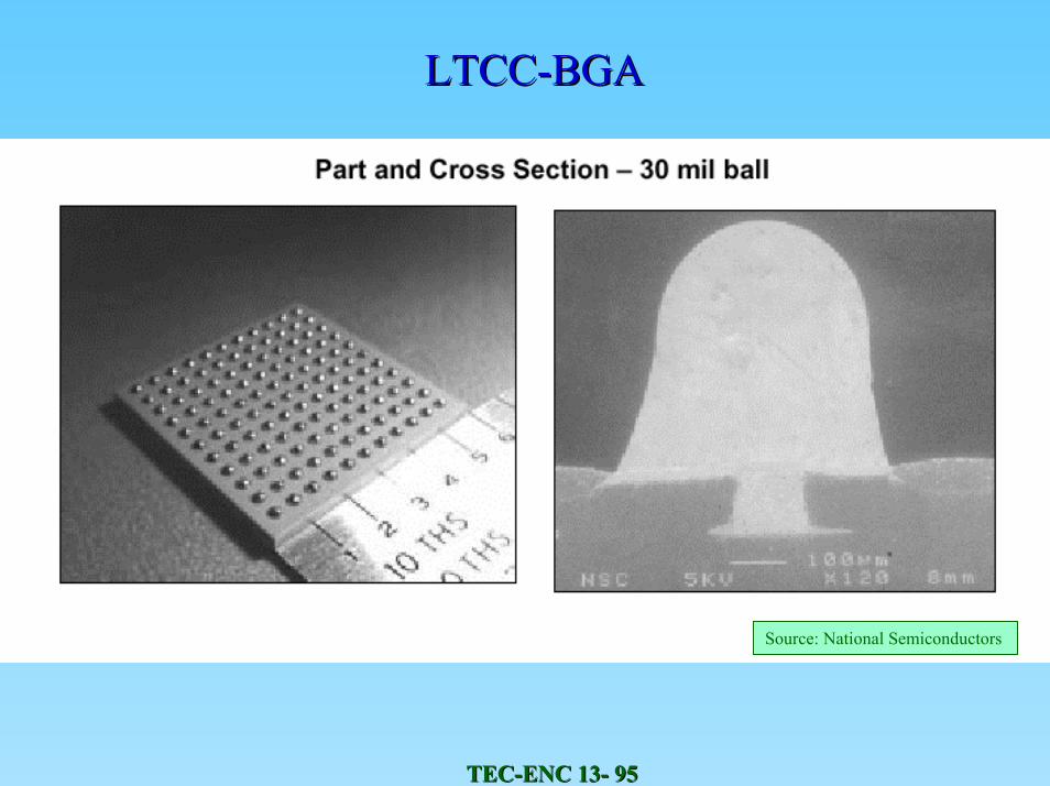
BALL GRID ARRAY WITH LTCCBALL GRID ARRAY WITH LTCC
• Advantages of BGA with LTCC
–High design flexibility–Very high number of I/Os
at reasonable pitch–High routing capability of
the LTCC
• Characteristics of BGA with LTCC
– Ball pitch from 0.75 mm to 1.5 mm– Body size from 5 x 5 mm2 to 40 x
40 mm2– Number of I/Os up to 961– High temperature solder balls– Adapted to single and multi-chip
module design– Large range of techniques for die
protection• Glued metallic or ceramic lid• Epoxy overmolding or glob top• Brazed hermetic Kovar ring
TECTEC--ENC 13ENC 13-- 9595
LTCCLTCC--BGABGA
Source: National Semiconductors
TECTEC--ENC 13ENC 13-- 9696
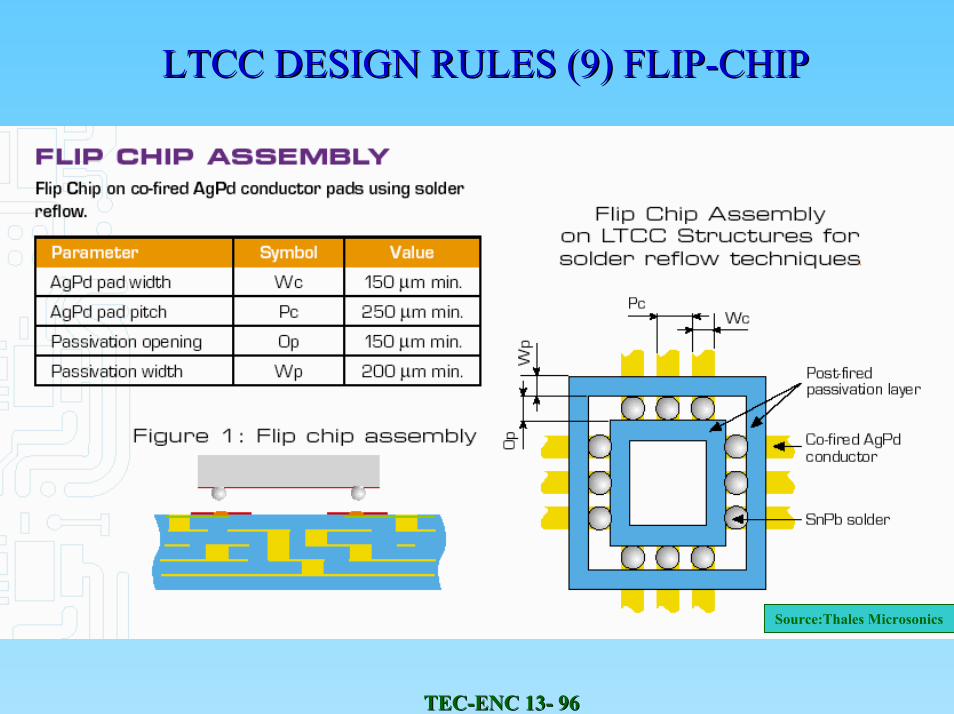
LTCC DESIGN RULES (9) FLIPLTCC DESIGN RULES (9) FLIP--CHIPCHIP
Source:Thales Microsonics
TECTEC--ENC 13ENC 13-- 9797
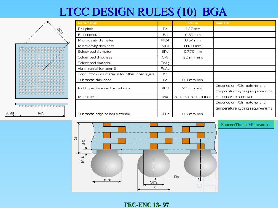
LTCC DESIGN RULES (10) BGALTCC DESIGN RULES (10) BGA
Source:Thales Microsonics
TECTEC--ENC 13ENC 13-- 9898
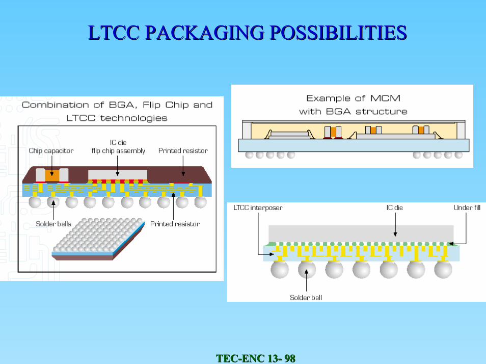
LTCC PACKAGING POSSIBILITIESLTCC PACKAGING POSSIBILITIES
TECTEC--ENC 13ENC 13-- 9999
LTCC PACKAGING APPLICATIONSLTCC PACKAGING APPLICATIONS


![Fwd: [juizesfree] ENC: Enc: Papagaios do Brasil](https://img.pdfslide.us/doc/110x75/5587e05ed8b42a15638b4725/fwd-juizesfree-enc-enc-papagaios-do-brasil.jpg)