Embed Size (px)
Citation preview

Team LuGERTeam LuGERLaser Guided Energy ReceiverLaser Guided Energy Receiver
Team LuGERTeam LuGERLaser Guided Energy ReceiverLaser Guided Energy Receiver
Jeremy AndersonMike WeimerRyan SchnellMike Wong
Jeremy AndersonMike WeimerRyan SchnellMike Wong
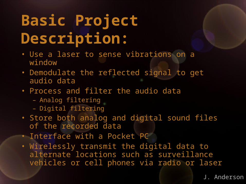
Basic Project Description:
• Use a laser to sense vibrations on a window• Demodulate the reflected signal to get audio data• Process and filter the audio data
– Analog filtering– Digital filtering
• Store both analog and digital sound files of the recorded data
• Interface with a Pocket PC • Wirelessly transmit the digital data to alternate
locations such as surveillance vehicles or cell phones via radio or laser
J. Anderson
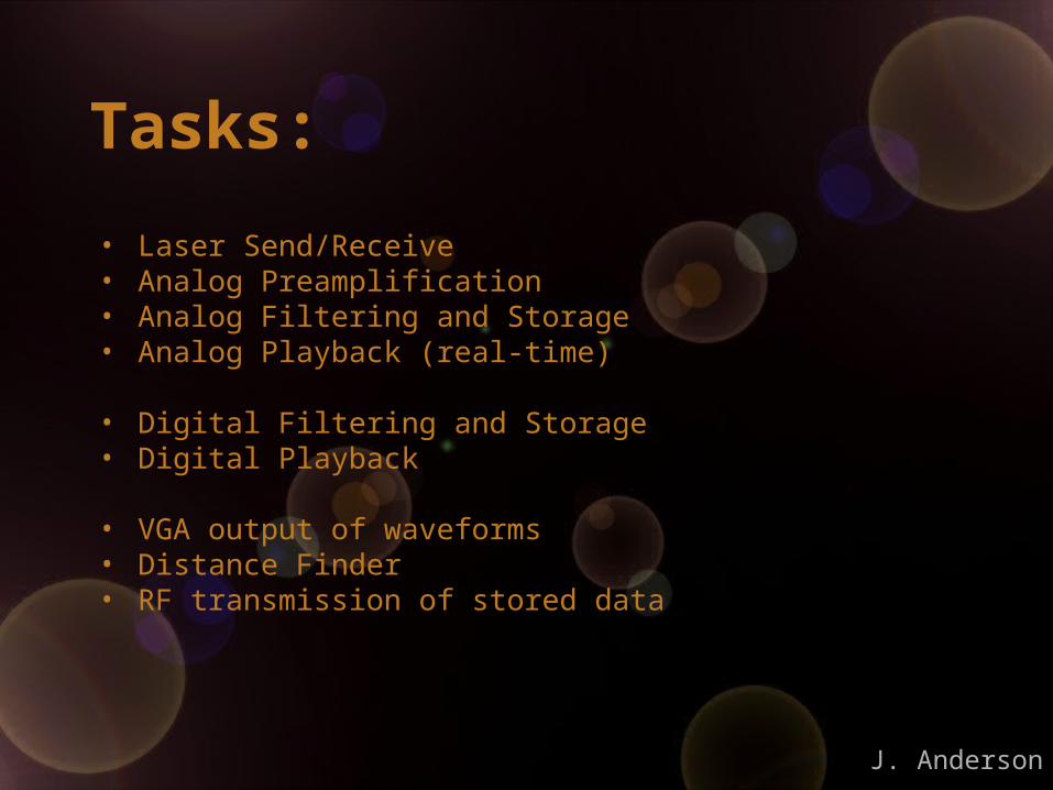
• Laser Send/Receive• Analog Preamplification• Analog Filtering and Storage• Analog Playback (real-time)
• Digital Filtering and Storage• Digital Playback
• VGA output of waveforms• Distance Finder• RF transmission of stored data
Tasks:
J. Anderson
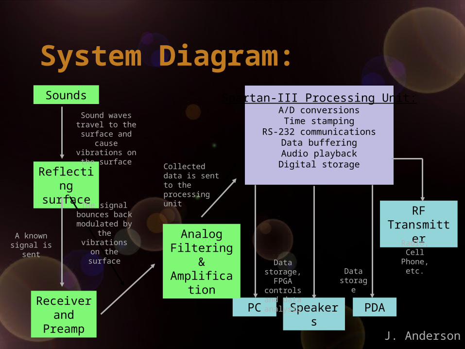
System Diagram:
A known signal is sent
Receiver and
Preamp
Reflecting surface
Sounds
Sound waves travel to the surface and
cause vibrations on the surface
The signal bounces back
modulated by the vibrations on the
surface
Spartan-III Processing Unit:A/D conversionsTime stamping
RS-232 communicationsData bufferingAudio playbackDigital storageCollected data
is sent to the processing unit
PC Speakers PDA
Data storage
Audio play back
Data storage, FPGA controls
and data analysis
Analog Filtering &
Amplification
RF Transmitter
Radio, Cell Phone, etc.
J. Anderson
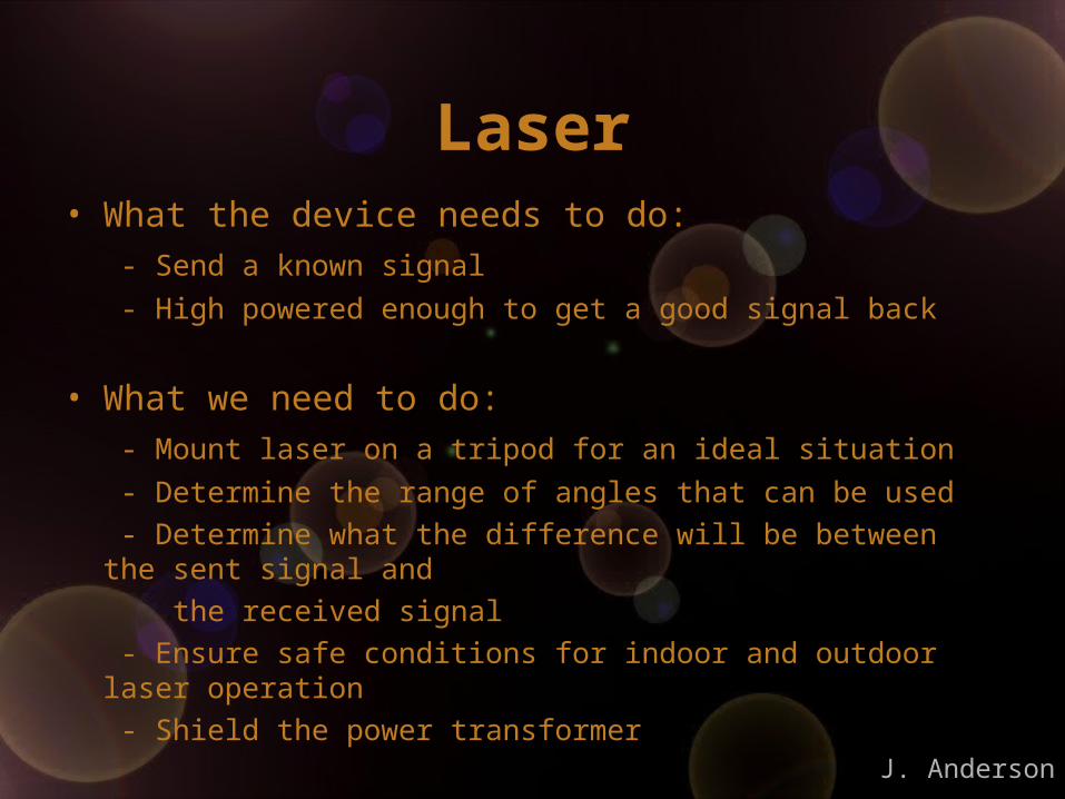
Laser• What the device needs to do:
- Send a known signal
- High powered enough to get a good signal back
• What we need to do:
- Mount laser on a tripod for an ideal situation
- Determine the range of angles that can be used
- Determine what the difference will be between the sent signal and
the received signal
- Ensure safe conditions for indoor and outdoor laser operation
- Shield the power transformer
J. Anderson
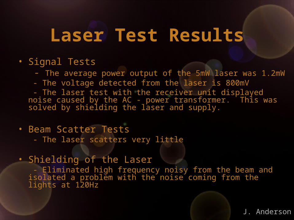
Laser Test Results• Signal Tests
- The average power output of the 5mW laser was 1.2mW - The voltage detected from the laser is 800mV - The laser test with the receiver unit displayed noise caused by the AC - power transformer. This was solved by shielding the laser and supply.
• Beam Scatter Tests - The laser scatters very little
• Shielding of the Laser - Eliminated high frequency noisy from the beam and isolated a problem with the noise coming from the lights at 120Hz
J. Anderson
J. Anderson
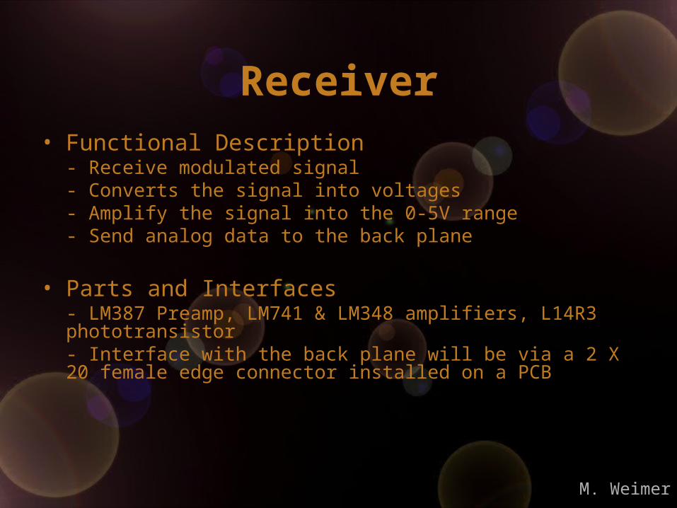
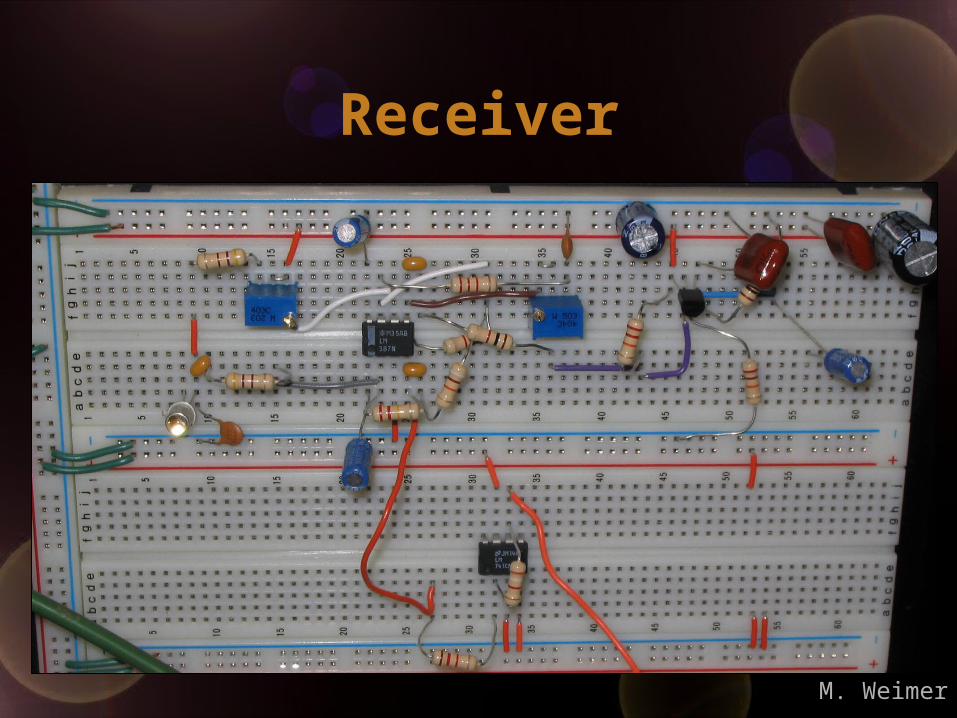
Receiver• Functional Description
- Receive modulated signal- Converts the signal into voltages- Amplify the signal into the 0-5V range- Send analog data to the back plane
• Parts and Interfaces- LM387 Preamp, LM741 & LM348 amplifiers, L14R3 phototransistor- Interface with the back plane will be via a 2 X 20 female edge connector installed on a PCB
M. Weimer
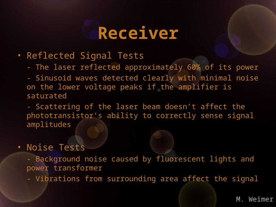
• Reflected Signal Tests- The laser reflected approximately 60% of its power
- Sinusoid waves detected clearly with minimal noise on the lower voltage peaks if the amplifier is saturated
- Scattering of the laser beam doesn’t affect the phototransistor’s ability to correctly sense signal amplitudes
• Noise Tests- Background noise caused by fluorescent lights and power transformer
- Vibrations from surrounding area affect the signal
Receiver
M. Weimer
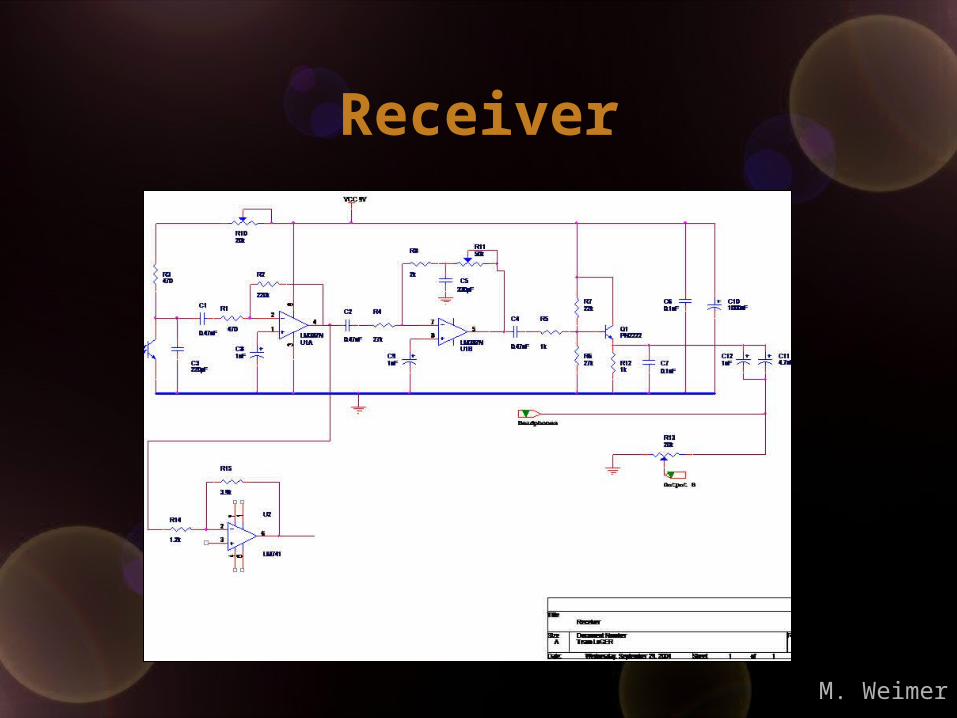
Receiver
M. Weimer
Receiver
M. Weimer
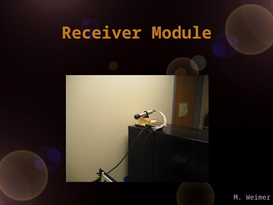
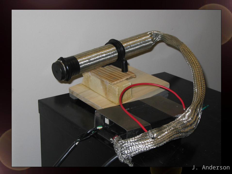
Receiver Module
M. Weimer
Analog Filtering
• Functional Description- Filters the analog signal from the receiver unit for audible human voices- Divide the signal into regions to correct frequency response problems
- Obtain signals in the 0-20KHz range - Bandstop filters - Signal Pumping Cards
• Parts and Interfaces- OP-amps for 2nd order Chebychev bandpass filters- Interfaces with the back plane through a 2X20 female edge connector
M. Weimer
Faux Equo• Functional Description
- Analog filters will use a high-pass filter on signals greater than 12KHz - Low-pass signals below 100Hz - Divide the remaining signal into 4 divisions: 100, 1K, 2K, 4K and 12K.
• Parts Lists and Interfaces - Op Amps, resistors, capacitors and circuit card construction - 2X20 female edge connectors
M. Weimer
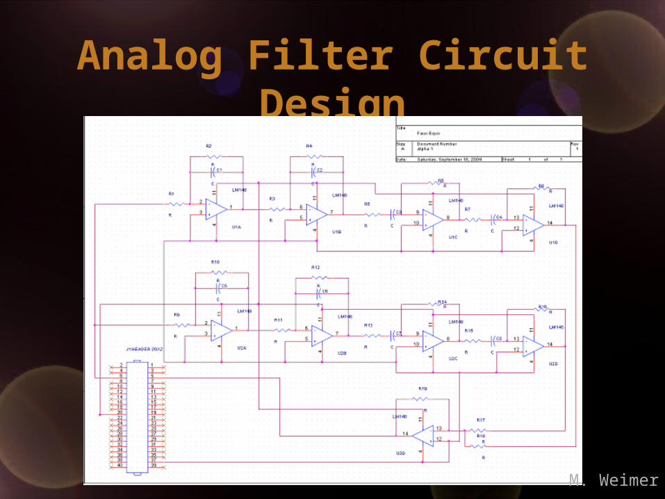
Analog Filter Circuit Design
M. Weimer
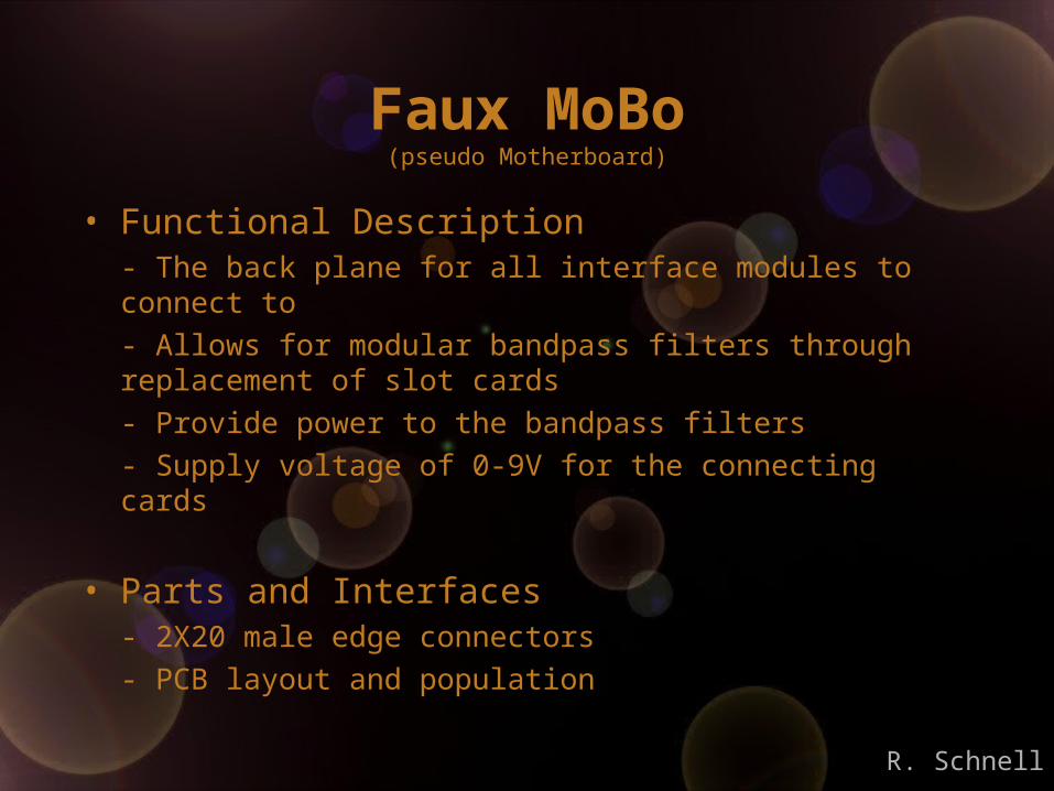
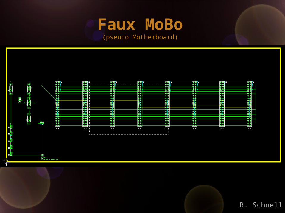
Faux MoBo(pseudo Motherboard)
• Functional Description- The back plane for all interface modules to connect to
- Allows for modular bandpass filters through replacement of slot cards
- Provide power to the bandpass filters
- Supply voltage of 0-9V for the connecting cards
• Parts and Interfaces- 2X20 male edge connectors
- PCB layout and population
R. Schnell
Faux MoBo(pseudo Motherboard)
R. Schnell
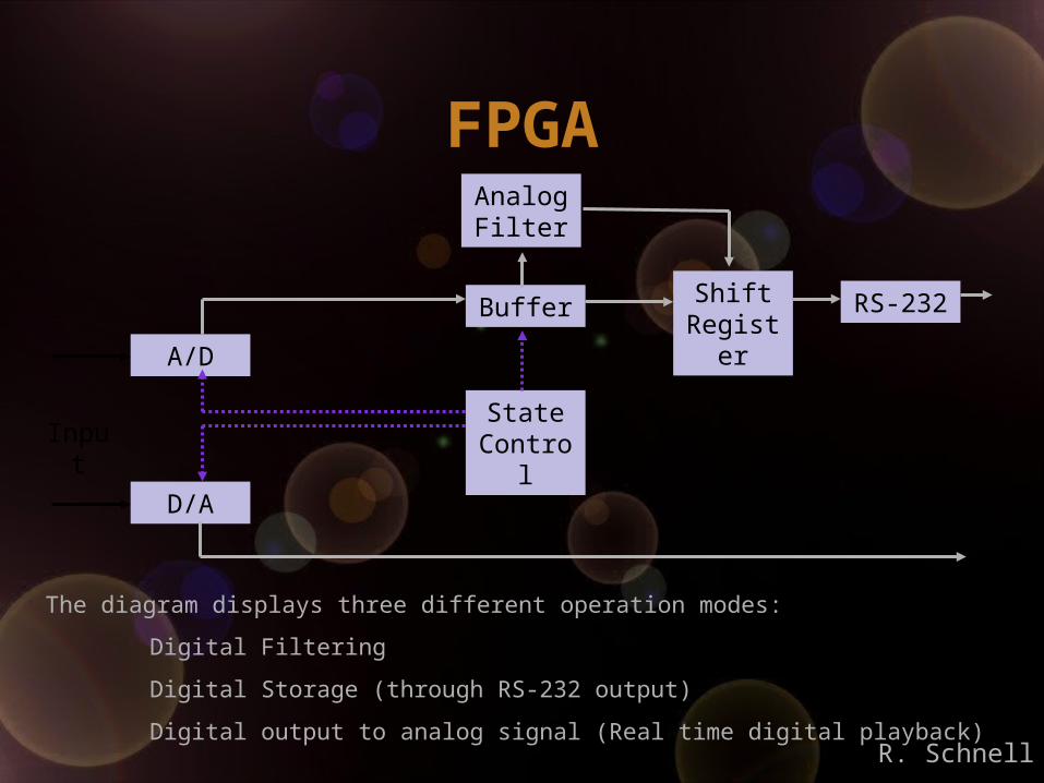
FPGA
A/D
D/A
Buffer
State Control
Shift Register
RS-232
Analog Filter
Input
The diagram displays three different operation modes:
Digital Filtering
Digital Storage (through RS-232 output)
Digital output to analog signal (Real time digital playback)R. Schnell
FPGA• Functional Description
- Receive the filtered data
- Buffer the data
- Control the communications between each modular unit
- Control of audio playback
• Parts and interfaces
- Connects to the back plane through female ribbon cables
R. Schnell
FPGA
R. Schnell
FPGA Test Results• I/O verification
- List of I/O verified- Confirmation of I/O voltage settings
• Memory Tests- FPGA and memory were programmed successfully- Use of the memory established
R. Schnell
DSP• Functional Description
- Will smooth digital signal
- Will provide squelch
- Possibly perform Fourier analysis
• Parts and Interfaces
- Verilog and schematics in Xilinx on FPGA
R. Schnell
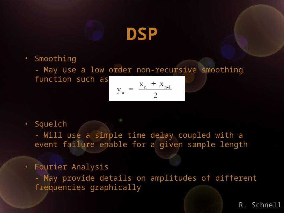
DSP• Smoothing
- May use a low order non-recursive smoothing function such as
• Squelch
- Will use a simple time delay coupled with a event failure enable for a given sample length
• Fourier Analysis
- May provide details on amplitudes of different frequencies graphically
R. Schnell
Sampling• Functional Description
- 8-bit A/D and 8-bit D/A converts
- 18.9K sampling rate, the same rate as a CD-ROM
- Send the sampled data to storage
• Parts and Interfaces
- MAX108, MAX533 and RAM
M. Wong
Communications• RS-232 Functional Description
- 56.6kbps rate will be use in conjunction with a data storage.
- 9 bit even parity
- Signal levels on the FauxMobo will utilize 0-9V and converter to RS-232 binary
• Tests Results - Verified control of outputs
M. Wong
Communications• What will be sent?
- Start string of 111111110 will start a “Chunk”
- Next 9 bits will be timestamp from last transmission in secs.
(deals with squelch)
- 9 bit even parity digital voltage value will be sent
• When will it be sent? - We will store the values to RAM, and send a string at 56.6k
across RS-232 serial cable to receiving computer/PDA after storage, and after a given signal.
- Eventually, if time allows, this will also be able to be sent via RF using same bit patterns.
M. Wong
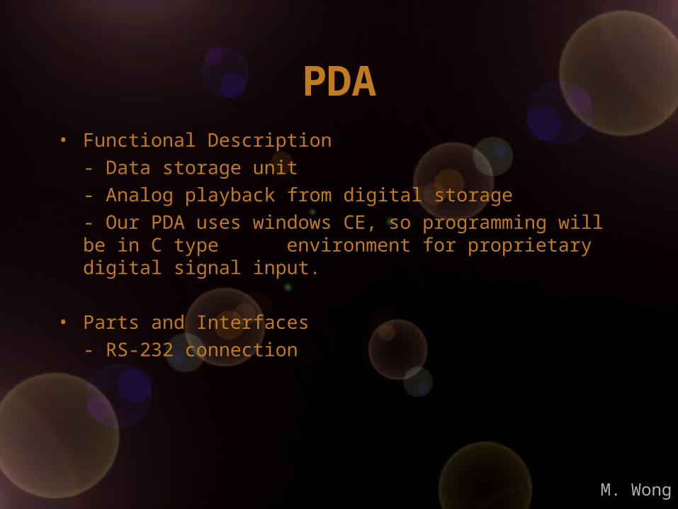
PDA• Functional Description
- Data storage unit
- Analog playback from digital storage
- Our PDA uses windows CE, so programming will be in C type environment for proprietary digital signal input.
• Parts and Interfaces
- RS-232 connection
M. Wong
ScheduleID Task Name Duration Start Finish
1 PDR presenation 0 days Tue 9/7/04 Tue 9/7/04
2 Preliminary user manual 5 days Wed 9/1/04 Tue 9/7/04
3 Laser mounting 14 days Mon 8/23/04 Thu 9/9/04
4 Initial design of analog filter 8 days Tue 8/31/04 Thu 9/9/04
5 Test plan of system 8 days Wed 9/8/04 Fri 9/17/04
6 Functional receiver unit 16 days Tue 8/31/04 Tue 9/21/04
7 Analog storage design 11 days Thu 9/9/04 Thu 9/23/04
8 Analog filtering functional 19 days Thu 9/9/04 Tue 10/5/04
9 Integration of receiver andFPGA
11 days Tue 9/21/04 Tue 10/5/04
10 CDR presentation 0 days Tue 10/5/04 Tue 10/5/04
11 Minimum functionality ofFPGA state machine
27 days Tue 9/7/04 Tue 10/12/04
12 Analog storage tested 16 days Fri 9/24/04 Thu 10/14/04
13 Modular interface complete 21 days Thu 9/23/04 Tue 10/19/04
14 Integration of modular unitwith receiver and FPGA
25 days Tue 9/21/04 Thu 10/21/04
15 Digital filtering and storagedesigned
11 days Tue 10/12/04 Mon 10/25/04
16 First Mile Stone 0 days Tue 10/26/04 Tue 10/26/04
17 Basic system completed 27 days Wed 9/22/04 Tue 10/26/04
18 Decide upon projectexpansions
3 days Tue 10/26/04 Thu 10/28/04
19 Preliminary technical manual 13 days Sun 10/17/04 Tue 11/2/04
20 Digital filtering, storage andplayback complete
16 days Wed 10/13/04 Tue 11/2/04
21 Second Milestone 0 days Tue 11/16/04 Tue 11/16/04
22 Complete project expansions 11 days Tue 11/2/04 Tue 11/16/04
23 Final technical manual 11 days Tue 11/2/04 Tue 11/16/04
24 Final testing 13 days Tue 11/16/04 Thu 12/2/04
25 Design expo 0 days Thu 12/9/04 Thu 12/9/04
9/7
10/5
10/26
11/16
12/9
22 25 28 31 3 6 9 12 15 18 21 24 27 30 3 6 9 12 15 18 21 24 27 30 2 5 8 11 14 17 20 23 26 29 2 5 8 11 14 17August 2004 September 2004 October 2004 November 2004 December 2004
M. Wong
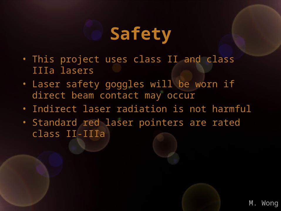
Safety• This project uses class II and class IIIa lasers• Laser safety goggles will be worn if direct beam
contact may occur• Indirect laser radiation is not harmful• Standard red laser pointers are rated class II-IIIa
M. Wong
Safety
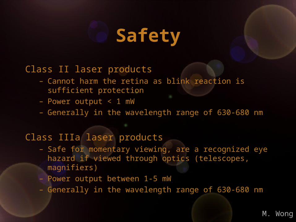
Class II laser products – Cannot harm the retina as blink reaction is sufficient
protection– Power output < 1 mW – Generally in the wavelength range of 630-680 nm
Class IIIa laser products – Safe for momentary viewing, are a recognized eye hazard if
viewed through optics (telescopes, magnifiers) – Power output between 1-5 mW– Generally in the wavelength range of 630-680 nm
M. Wong
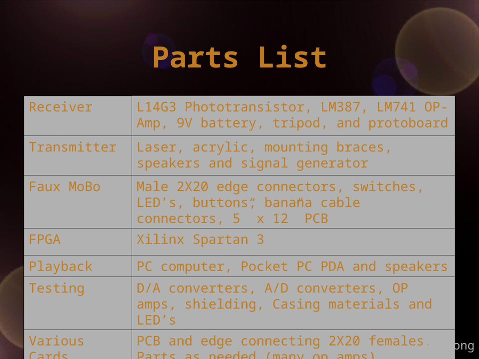
Parts List
Receiver L14G3 Phototransistor, LM387, LM741 OP-Amp, 9V battery, tripod, and protoboard
Transmitter Laser, acrylic, mounting braces, speakers and signal generator
Faux MoBo Male 2X20 edge connectors, switches, LED’s, buttons, banana cable connectors, 5” x 12” PCB
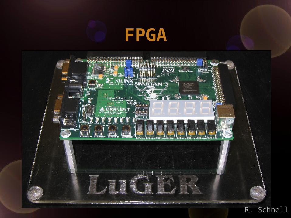
FPGA Xilinx Spartan 3
Playback PC computer, Pocket PC PDA and speakers
Testing D/A converters, A/D converters, OP amps, shielding, Casing materials and LED’s
Various Cards PCB and edge connecting 2X20 females. Parts as needed (many op amps)
M. Wong
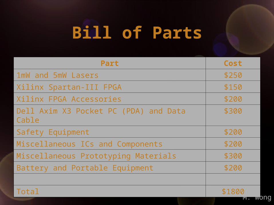
Bill of Parts
Part Cost
1mW and 5mW Lasers $250
Xilinx Spartan-III FPGA $150
Xilinx FPGA Accessories $200
Dell Axim X3 Pocket PC (PDA) and Data Cable $300
Safety Equipment $200
Miscellaneous ICs and Components $200
Miscellaneous Prototyping Materials $300
Battery and Portable Equipment $200
Total $1800
M. Wong

Division of Labor• Ryan Schnell
- FPGA Programming
- Modular Unit Interface
- Analog filter design
- Faux MoBo design
• Mike Wong- FPGA Programming
- Faux MoBo layout
- Test plans
- CDR presentation
• Mike Weimer- Receiver power supply
- Analog filter testing
- Parts procurement
- Receiver testing
- Silkscreening of CU logo and Scooby Doo on PCB
• Jeremy Anderson- RX and TX with PC
- User manual
- Accounting funds
- Receiver testing
M. Wong
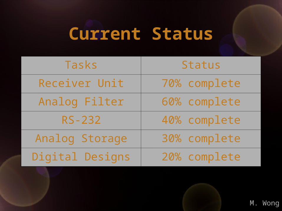
Current Status
Tasks Status
Receiver Unit 70% complete
Analog Filter 60% complete
RS-232 40% complete
Analog Storage 30% complete
Digital Designs 20% complete
M. Wong